Embed Size (px)
Citation preview
1 REV: 120407
Note: Some revisions of this device may incorporate deviations from published specifications known as errata. Multiple revisions of any device may be simultaneously available through various sales channels. For information about device errata, click here: www.maxim-ic.com/errata.
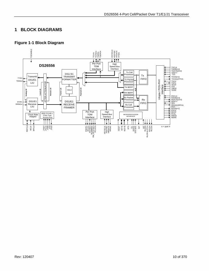
GENERAL DESCRIPTION The DS26556 is a quad, software-selectable T1, E1, or J1 transceiver with a cell/packet/TDM interface. It is composed of four framer/formatters + LIUs, and a UTOPIA (cell), POS-PHY™ (packet), and TDM backplane interface. Each framer has an HDLC controller that can be mapped to any DS0 or FDL (T1)/Sa (E1) bit. The DS26556 also includes full-featured BERT devices per port, and an internal clock adapter useful for creating synchronous, high-frequency backplane timing. The DS26556 is controlled through an 8-bit parallel port that can be configured for nonmultiplexed Intel or Motorola operation. APPLICATIONS Routers IMA
Add-Drop Multiplexers ATM
DSLAMs WAN Interface
PBXs
Switches
Customer-Premise Equipment
Central Office Equipment
POS-PHY and POS-PHY Level 3 are trademarks of PMC-Sierra, Inc.
FEATURES
Four Independent, Full-Featured T1/E1/J1 Transceivers
UTOPIA 2 and 3 Cell Interface
POS-PHY 2 and 3 Packet Interface
TDM Backplane Supports TDM Bus Rates from 1.544MHz to 16.384MHz
Alarm Detection and Insertion
Full-Featured BERT for Each Port
AMI, B8ZS, HDB3, NRZ Line Coding
Transmit Synchronizer
BOC Message Controller (T1)
One HDLC Controller per Framer
Performance Monitor Counters
RAI-CI and AIS-CI Support
Internal Clock Generator (CLAD) Supplies 16.384MHz, 8.192MHz, 4.096MHz, or 2.048MHz
JTAG Test Port
Single 3.3V Supply with 5V Tolerant Inputs
17mm x 17mm, 256-Pin CSBGA (1.00mm Pitch)
ORDERING INFORMATION
PART TEMP RANGE PIN-PACKAGE
DS26556 0°C to +70°C 256 CSBGA
DS26556N -40°C to +85°C 256 CSBGA
DS265564-Port Cell/Packet Over T1/E1/J1
Transceiverwww.maxim-ic.com
DS26556 4-Port Cell/Packet Over T1/E1/J1 Transceiver
Rev: 120407 2 of 370
TABLE OF CONTENTS 1 BLOCK DIAGRAMS 10 2 FEATURES 11
2.1 FRAMER/LIU ................................................................................................................................................11 2.1.1 Framer/Formatter ................................................................................................................................................11 2.1.2 Line Interface (LIU) .............................................................................................................................................11 2.1.3 Clock Synthesizer ...............................................................................................................................................12 2.1.4 HDLC Controllers ................................................................................................................................................12 2.1.5 Test and Diagnostics...........................................................................................................................................12
2.2 CELL/PACKET INTERFACE .............................................................................................................................12 2.2.1 General ...............................................................................................................................................................12 2.2.2 ATM ....................................................................................................................................................................13 2.2.3 HDLC ..................................................................................................................................................................13
2.3 CONTROL PORT ...........................................................................................................................................13 3 BACKPLANE CONFIGURATION SCENARIOS 15 4 ACRONYMS AND GLOSSARY 19 5 PIN DESCRIPTIONS 20
5.1 SHORT PIN LIST ...........................................................................................................................................20 5.2 DETAILED PIN LIST .......................................................................................................................................24
6 DEVICE CONFIGURATION 32 7 FUNCTIONAL PIN TIMING 33
7.1 RECEIVER FUNCTIONAL TIMING DIAGRAMS ....................................................................................................33 7.2 TRANSMITTER FUNCTIONAL TIMING DIAGRAMS...............................................................................................34 7.3 UTOPIA/POS-PHY/SPI-3 SYSTEM INTERFACE FUNCTIONAL TIMING.............................................................36
7.3.1 UTOPIA Level 2 Functional Timing.....................................................................................................................36 7.3.2 UTOPIA Level 3 Functional Timing.....................................................................................................................40 7.3.3 POS-PHY Level 2 Functional Timing ..................................................................................................................43 7.3.4 POS-PHY Level 3 Functional Timing ..................................................................................................................47
8 FUNCTIONAL DESCRIPTION 49 8.1 CELL / PACKET INTERFACE DESCRIPTION ......................................................................................................49
8.1.1 Reset Descriptions..............................................................................................................................................49 8.1.2 BIT / BYTE Ordering ...........................................................................................................................................49
8.2 UTOPIA/POS-PHY/SPI-3 SYSTEM INTERFACE............................................................................................49 8.2.1 General Description ............................................................................................................................................49 8.2.2 Features..............................................................................................................................................................50 8.2.6 System Interface Bus Controller .........................................................................................................................50
8.3 ATM CELL / HDLC PACKET PROCESSING.....................................................................................................54 8.3.1 General Description ............................................................................................................................................54 8.3.2 Features..............................................................................................................................................................54 8.3.3 Transmit Cell/Packet Processor ..........................................................................................................................55 8.3.4 Receive Cell/Packet Processor ...........................................................................................................................55 8.3.5 Cell Processor.....................................................................................................................................................56 8.3.6 Packet Processor................................................................................................................................................61 8.3.7 FIFO....................................................................................................................................................................63 8.3.8 System Loopback................................................................................................................................................64
8.4 T1 RECEIVE FRAMER DESCRIPTION AND OPERATION .....................................................................................65 8.4.1 T1 Loopbacks .....................................................................................................................................................65 8.4.2 H.100 (CT Bus) Compatibility..............................................................................................................................66 8.4.3 T1 Receive Status and Information .....................................................................................................................67 8.4.4 Receive AIS-CI and RAI-CI Detection.................................................................................................................69 8.4.5 T1 Receive-Side Digital Milliwatt Code Generation.............................................................................................69 8.4.6 T1 Error Count Registers ....................................................................................................................................69 8.4.7 T1 Receive Signaling Operation..........................................................................................................................70 8.4.8 Software Signaling ..............................................................................................................................................70 8.4.9 Hardware Signaling.............................................................................................................................................70 8.4.10 Signaling Re-insertion .........................................................................................................................................70 8.4.11 Receive Signaling Freeze ...................................................................................................................................71 8.4.12 Fractional T1 Support (Gapped-Clock Mode) .....................................................................................................71 8.4.13 T1 Bit-Oriented Code (BOC) Controller...............................................................................................................71
DS26556 4-Port Cell/Packet Over T1/E1/J1 Transceiver
Rev: 120407 3 of 370
8.4.14 Receive SLC-96 Operation .................................................................................................................................71 8.4.15 Receive FDL .......................................................................................................................................................71 8.4.16 Programmable In-Band Loop-Code Detection ....................................................................................................72 8.4.17 Receive HDLC Controller....................................................................................................................................72 8.4.18 Receive HDLC Controller Example .....................................................................................................................73
8.5 T1 TRANSMIT FORMATTER DESCRIPTION AND OPERATION .............................................................................74 8.5.1 T1 Per-Channel Loopback ..................................................................................................................................74 8.5.2 T1 Transmit DS0 Monitoring Function.................................................................................................................74 8.5.3 T1 Transmit Signaling Operation.........................................................................................................................74 8.5.4 T1 Transmit Per-Channel Idle Code Insertion.....................................................................................................75 8.5.5 T1 Transmit Channel Mark Registers..................................................................................................................75 8.5.6 Fractional T1 Support (Gapped Clock Mode)......................................................................................................75 8.5.7 T1 Transmit Bit Oriented Code (BOC) Controller ................................................................................................75 8.5.8 T1 Transmit FDL .................................................................................................................................................75 8.5.9 Transmit SLC–96 Operation ...............................................................................................................................76 8.5.10 Transmit HDLC Controller...................................................................................................................................76 8.5.11 HDLC Transmit Example ....................................................................................................................................76 8.5.12 Programmable In-Band Loop-Code Generator ...................................................................................................77 8.5.13 Interfacing the T1 Tx Formatter to the BERT ......................................................................................................78 8.5.14 T1 Transmit Synchronizer ...................................................................................................................................78
8.6 E1 RECEIVE FRAMER DESCRIPTION AND OPERATION.....................................................................................78 8.6.1 H.100 (CT Bus) Compatibility..............................................................................................................................78 8.6.2 E1 Error Count Registers ....................................................................................................................................79 8.6.3 DS0 Monitoring Function.....................................................................................................................................80 8.6.4 E1 Receive Signaling Operation .........................................................................................................................80 8.6.5 Fractional E1 Support (Gapped Clock Mode) .....................................................................................................81 8.6.6 Additional Sa-Bit and Si-Bit Receive Operation (E1 Mode).................................................................................81 8.6.7 HDLC Overhead Control Receive Example ........................................................................................................81 8.6.8 Interfacing the E1 Rx Framer to the BERT..........................................................................................................82 8.6.9 E1 Transmit Formatter Description and Operation..............................................................................................83 8.6.10 Automatic Alarm Generation ...............................................................................................................................83 8.6.11 G.706 Intermediate CRC-4 Updating (E1 Mode Only) ........................................................................................83 8.6.12 E1 Transmit DS0 Monitoring Function ................................................................................................................84 8.6.13 E1 Transmit Signaling Operation ........................................................................................................................84 8.6.14 Fractional E1 Support (Gapped Clock Mode) .....................................................................................................85 8.6.15 Additional (Sa) and International (Si) Bit Operation (E1 Mode) ...........................................................................85 8.6.16 E1 Transmit HDLC Controller .............................................................................................................................85 8.6.17 E1 HDLC Transmit Example ...............................................................................................................................86 8.6.18 Interfacing the E1 Transmitter to the BERT ........................................................................................................87 8.6.19 E1 Transmit Synchronizer ...................................................................................................................................87
9 LINE INTERFACE UNIT (LIU) 88 9.1 LIU TRANSMITTER........................................................................................................................................88
9.1.1 Pulse Shapes ...................................................................................................................................................88 9.1.2 Transmit Termination ......................................................................................................................................88 9.1.3 Power-Down and High-Z ................................................................................................................................88 9.1.4 Transmit All Ones ............................................................................................................................................88 9.1.5 Driver Fail Monitor ...........................................................................................................................................88
9.2 RECEIVER ....................................................................................................................................................91 9.2.1 Receiver Monitor Mode...................................................................................................................................91 9.2.2 Peak Detector and Slicer................................................................................................................................91 9.2.3 Clock and Data Recovery...............................................................................................................................91 9.2.4 Receive Level Indicator ..................................................................................................................................91 9.2.5 Loss of Signal...................................................................................................................................................92
9.3 JITTER ATTENUATOR ....................................................................................................................................94 9.4 LIU LOOPBACKS...........................................................................................................................................95
9.4.1 Analog Loopback ................................................................................................................................................95 9.4.2 Local Loopback...................................................................................................................................................95 9.4.3 Remote Loopback ...............................................................................................................................................95
10 OVERALL REGISTER MAP 96 11 REGISTER MAPS AND DESCRIPTIONS 98
11.1 GLOBAL REGISTERS .....................................................................................................................................98 11.1.1 Global Control Registers .....................................................................................................................................98
DS26556 4-Port Cell/Packet Over T1/E1/J1 Transceiver
Rev: 120407 4 of 370
11.1.2 Global Status Registers ....................................................................................................................................105 11.2 CELL/PACKET REGISTER DESCRIPTIONS .....................................................................................................111
11.2.1 General Cell / Packet Registers ........................................................................................................................112 11.2.2 Cell/Packet Status Registers.............................................................................................................................114 11.2.3 Transmit FIFO Registers...................................................................................................................................116 11.2.4 Transmit Cell Processor Registers....................................................................................................................121 11.2.5 Transmit Packet Processor Registers ...............................................................................................................129 11.2.6 Receive Cell Processor Registers.....................................................................................................................135 11.2.7 Receive Packet Processor Registers ................................................................................................................150 11.2.8 Receive FIFO Registers....................................................................................................................................162
11.3 SYSTEM INTERFACE REGISTERS..................................................................................................................165 11.3.1 Transmit System Interface Registers ................................................................................................................165 11.3.2 Receive System Interface Registers .................................................................................................................168
11.4 RECEIVE T1 FRAMER REGISTERS ...............................................................................................................171 11.4.1 Receive Master-Mode Register.........................................................................................................................174 11.4.2 Interrupt Information Register ...........................................................................................................................175 11.4.3 T1 Receive Control Registers ...........................................................................................................................176 11.4.4 T1 Line-Code Violation Count Register (LCVCR) .............................................................................................192 11.4.5 T1 Path-Code Violation Count Register (PCVCR) ............................................................................................193 11.4.6 T1 Frames Out-of-Sync Count Register (FOSCR)............................................................................................194 11.4.7 DS0 Monitoring Function...................................................................................................................................195 11.4.8 Receive Signaling Registers .............................................................................................................................196 11.4.9 T1 Receive Per-Channel Idle Code Insertion....................................................................................................199 11.4.10 T1 Receive Channel Mark Registers.................................................................................................................200 11.4.11 Receive Fractional T1 Support (Gapped-Clock Mode)......................................................................................201 11.4.12 Receive T1 Bit-Oriented Code (BOC) Controller...............................................................................................202 11.4.13 Receive SLC-96 Operation ...............................................................................................................................203 11.4.14 Receive FDL .....................................................................................................................................................204 11.4.15 Programmable In-Band Loop-Code Detection ..................................................................................................205 11.4.16 Receive HDLC Controller..................................................................................................................................211 11.4.17 Receive BERT ..................................................................................................................................................217
11.5 T1 TRANSMIT FRAMER................................................................................................................................219 11.5.1 Transmit-Master Mode Register........................................................................................................................222 11.5.2 Interrupt Information Registers..........................................................................................................................222 11.5.3 T1 Transmit Control Registers ..........................................................................................................................223 11.5.4 T1 Transmit Status and Information ..................................................................................................................228 11.5.5 T1 Per-Channel Loopback ................................................................................................................................231 11.5.6 T1 Transmit DS0 Monitoring Function...............................................................................................................232 11.5.7 T1 Transmit Signaling Operation.......................................................................................................................232 11.5.8 T1 Transmit Per-Channel Idle Code Insertion...................................................................................................236 11.5.9 T1 Transmit Channel Mark Registers................................................................................................................238 11.5.10 Fractional T1 Support (Gapped Clock Mode)....................................................................................................240 11.5.11 T1 Transmit Bit Oriented Code (BOC) Controller ..............................................................................................240 11.5.12 T1 Transmit FDL ...............................................................................................................................................242 11.5.13 Transmit SLC–96 Operation .............................................................................................................................242 11.5.14 Transmit HDLC Controller.................................................................................................................................243 Transmit Interrupt Mask Register 2 .................................................................................................................................248 11.5.15 Programmable In-Band Loop-Code Generator .................................................................................................250 11.5.16 Interfacing the T1 Tx Formatter to the BERT ....................................................................................................252 11.5.17 T1 Transmit Synchronizer .................................................................................................................................254
11.6 E1 RECEIVE FRAMER .................................................................................................................................256 11.6.1 E1 Receive Framer Description and Operation.................................................................................................259 11.6.2 Receive Master Mode Register .........................................................................................................................259 11.6.3 Interrupt Information Registers..........................................................................................................................261 11.6.4 E1 Receive Control Registers ...........................................................................................................................261 11.6.5 E1 Receive Status and Information...................................................................................................................266 11.6.6 E1 Error Count Registers ..................................................................................................................................277 11.6.7 DS0 Monitoring Function...................................................................................................................................280 11.6.8 E1 Receive Signaling Operation .......................................................................................................................281 11.6.9 E1 Receive Per-Channel Idle Code Insertion....................................................................................................283 11.6.10 E1 Receive Channel Mark Registers ................................................................................................................284 11.6.11 Fractional E1 Support (Gapped Clock Mode) ...................................................................................................285 11.6.12 Additional Sa-Bit and Si-Bit Receive Operation (E1 Mode)...............................................................................286 11.6.13 Receive Framer HDLC Controller .....................................................................................................................292 11.6.14 Interfacing the E1 Rx Framer to the BERT........................................................................................................299
DS26556 4-Port Cell/Packet Over T1/E1/J1 Transceiver
Rev: 120407 5 of 370
11.7 E1 TRANSMIT FRAMER ...............................................................................................................................301 11.7.1 Transmit Master Mode Register ........................................................................................................................304 11.7.2 Interrupt Information Registers..........................................................................................................................305 11.7.3 E1 Transmit Control Registers ..........................................................................................................................305 11.7.4 E1 Transmit Status and Information..................................................................................................................309 11.7.5 Per-Channel Loopback .....................................................................................................................................310 11.7.6 E1 Transmit DS0 Monitoring Function ..............................................................................................................311 11.7.7 E1 Transmit Signaling Operation ......................................................................................................................312 11.7.8 E1 Transmit Per-Channel Idle Code Insertion...................................................................................................316 11.7.9 E1 Transmit Channel Mark Registers ...............................................................................................................317 11.7.10 Fractional E1 Support (Gapped Clock Mode) ...................................................................................................318 11.7.11 Additional (Sa) and International (Si) Bit Operation (E1 Mode) .........................................................................318 11.7.12 E1 Transmit HDLC Controller ...........................................................................................................................325 11.7.13 Interfacing the E1 Transmitter to the BERT ......................................................................................................331 11.7.14 E1 Transmit Synchronizer .................................................................................................................................332
12 LINE INTERFACE UNIT (LIU) 334 12.1 LIU REGISTERS..........................................................................................................................................334
13 BIT ERROR RATE TESTER (BERT) 341 13.1 BERT REGISTER BIT DESCRIPTIONS...........................................................................................................342
14 JTAG BOUNDARY SCAN ARCHITECTURE AND TEST ACCESS PORT 349 14.1 TAP CONTROLLER STATE MACHINE............................................................................................................350
14.1.1 Test-Logic-Reset...............................................................................................................................................351 14.1.2 Run-Test-Idle ....................................................................................................................................................351 14.1.3 Select-DR-Scan ................................................................................................................................................351 14.1.4 Capture-DR.......................................................................................................................................................351 14.1.5 Shift-DR ............................................................................................................................................................351 14.1.6 Exit1-DR............................................................................................................................................................351 14.1.7 Pause-DR .........................................................................................................................................................351 14.1.8 Exit2-DR............................................................................................................................................................351 14.1.9 Update-DR........................................................................................................................................................351 14.1.10 Select-IR-Scan..................................................................................................................................................351 14.1.11 Capture-IR ........................................................................................................................................................352 14.1.12 Shift-IR..............................................................................................................................................................352 14.1.13 Exit1-IR .............................................................................................................................................................352 14.1.14 Pause-IR ...........................................................................................................................................................352 14.1.15 Exit2-IR .............................................................................................................................................................352 14.1.16 Update-IR..........................................................................................................................................................352
14.2 INSTRUCTION REGISTER .............................................................................................................................353 14.2.1 SAMPLE/PRELOAD .........................................................................................................................................353 14.2.2 BYPASS............................................................................................................................................................353 14.2.3 EXTEST............................................................................................................................................................353 14.2.4 CLAMP..............................................................................................................................................................353 14.2.5 HIGHZ...............................................................................................................................................................353 14.2.6 IDCODE............................................................................................................................................................353
14.3 TEST REGISTERS........................................................................................................................................354 14.3.1 Boundary Scan Register ...................................................................................................................................354 14.3.2 Bypass Register................................................................................................................................................354 14.3.3 Identification Register........................................................................................................................................354
15 PIN ASSIGNMENT 355 16 PACKAGE INFORMATION 356
16.1 256-BALL TE-CSBGA (56-G6028-001).....................................................................................................356 17 THERMAL INFORMATION 357 18 ABSOLUTE MAXIMUM RATINGS 358 19 AC TIMING 359
19.1 TRANSMIT TDM PORT AC CHARACTERISTICS .............................................................................................361 19.2 RECEIVE TDM PORT AC CHARACTERISTICS ...............................................................................................362 19.3 HIGH-SPEED PORT AC CHARACTERISTICS ..................................................................................................363 19.4 SYSTEM INTERFACE AC CHARACTERISTICS .................................................................................................364 19.5 MICROPROCESSOR BUS AC CHARACTERISTICS...........................................................................................366 19.6 JTAG INTERFACE TIMING ...........................................................................................................................369

DS26556 4-Port Cell/Packet Over T1/E1/J1 Transceiver
Rev: 120407 6 of 370
20 DOCUMENT REVISION HISTORY 370
DS26556 4-Port Cell/Packet Over T1/E1/J1 Transceiver
Rev: 120407 7 of 370
LIST OF FIGURES Figure 1-1 Block Diagram.......................................................................................................................................... 10 Figure 2-1 Backplane Interface Diagram For Port 1 of 4........................................................................................... 14 Figure 3-1 ATM Over 4 Ports..................................................................................................................................... 15 Figure 3-2 IP Over 4 T1/E1 Ports .............................................................................................................................. 15 Figure 3-3 IP Over 2 Ports, TDM Over 2 Ports.......................................................................................................... 15 Figure 3-4 ATM Over 2 Ports, 2 Ports Combined Into High Speed TDM.................................................................. 15 Figure 3-5 Fractional ATM Over 4 Ports With Fractional TDM Access to Each Port................................................ 16 Figure 3-6 8 Port High Speed TDM Bus.................................................................................................................... 16 Figure 7-1 Receive TDM Signals............................................................................................................................... 33 Figure 7-2 Receive TDM Signals, Details.................................................................................................................. 33 Figure 7-3 Transmit TDM Signals.............................................................................................................................. 34 Figure 7-4 Transmit TDM Signals, Details................................................................................................................. 34 Figure 7-5 Two Port High Speed TDM Bus............................................................................................................... 35 Figure 7-6 Four Port High Speed TDM Bus .............................................................................................................. 36 Figure 7-7 UTOPIA Level 2 Transmit Cell Transfer Direct Mode.............................................................................. 37 Figure 7-8 UTOPIA Level 2 Receive Cell Transfer Direct Mode............................................................................... 37 Figure 7-9 UTOPIA Level 2 Transmit Multiple Cell Transfer Polled Mode................................................................ 38 Figure 7-10 UTOPIA Level 2 Receive Multiple Cell Transfer Polled Mode............................................................... 39 Figure 7-11 UTOPIA Level 2 Receive Unexpected Multiple Cell Transfer ............................................................... 39 Figure 7-12 UTOPIA Level 3 Transmit Multiple Cell Transfer Direct Mode .............................................................. 40 Figure 7-13 UTOPIA Level 3 Transmit Multiple Cell Transfer Polled Mode.............................................................. 41 Figure 7-14 UTOPIA Level 3 Receive Multiple Cell Transfer Direct Mode ............................................................... 42 Figure 7-15 UTOPIA Level 3 Receive Multiple Cell Transfer Polled Mode............................................................... 42 Figure 7-16 Transmit Multiple Packet Transfer to Different PHY ports (direct status mode).................................... 43 Figure 7-17 POS-PHY Level 2 Receive Multiple Packet Transfer from Different PHY Ports/Devices (direct status
mode) ................................................................................................................................................................ 44 Figure 7-18 POS-PHY Level 2 Transmit Multiple Packet Transfer to Different PHY Ports (polled status mode)..... 45 Figure 7-19 POS-PHY Level 2 Receive Multiple Packet Transfer (polled status mode) .......................................... 46 Figure 7-20 POS-PHY Level 3 Transmit Multiple Packet Transfer In-Band Addressing .......................................... 47 Figure 7-21 POS-PHY Level 3 Receive Multiple Packet Transfer In-Band Addressing ........................................... 48 Figure 8-1 Normal Packet Format in 16-Bit Mode..................................................................................................... 50 Figure 8-2 Byte Reordered Packet Format in 16-Bit Mode ....................................................................................... 51 Figure 8-3 Receive DSS Scrambler Synchronization State Diagram ....................................................................... 58 Figure 8-4 Cell Delineation State Diagram................................................................................................................ 59 Figure 8-5 HEC Error Monitoring State Diagram....................................................................................................... 60 Figure 8-6 Cell Format for 53-Byte Cell With 16-Bit Data Bus .................................................................................. 60 Figure 8-7 Cell Format for 52-Byte Cell With 16-Bit Data Bus .................................................................................. 61 Figure 8-8 Remote Loopback .................................................................................................................................... 65 Figure 8-9 Payload Loopback.................................................................................................................................... 66 Figure 8-10 Framer Loopback ................................................................................................................................... 66 Figure 8-11 HSSYNC Input in H.100 (CT Bus) Mode ............................................................................................... 67 Figure 8-12 Receive HDLC Example ........................................................................................................................ 73 Figure 8-13 HDLC Message Transmit Example........................................................................................................ 77 Figure 8-14 HSSYNC Input in H.100 (CT Bus) Mode ............................................................................................... 79 Figure 8-15 Receive HDLC Example ........................................................................................................................ 82 Figure 8-16 CRC Update Flow Diagram ................................................................................................................... 84 Figure 8-17 Time Slot Numbering Schemes ............................................................................................................. 85 Figure 8-18 E1 HDLC Message Transmit Example .................................................................................................. 86 Figure 9-1 T1/J1 Transmit Pulse Templates ............................................................................................................. 89 Figure 9-2 E1 Transmit Pulse Templates .................................................................................................................. 90 Figure 9-3 Typical Monitor Operation ........................................................................................................................ 91 Figure 9-4 Jitter Tolerance ........................................................................................................................................ 93 Figure 9-5 Jitter Attenuation ...................................................................................................................................... 94 Figure 11-1 Transmit FIFO Register Map................................................................................................................ 116 Figure 11-2 E1 Sync/Resync Criteria ...................................................................................................................... 262 Figure 14-1 JTAG Functional Block Diagram.......................................................................................................... 349 Figure 14-2 TAP Controller State Diagram.............................................................................................................. 350
DS26556 4-Port Cell/Packet Over T1/E1/J1 Transceiver
Rev: 120407 8 of 370
Figure 15-1 DS26556 Pin Assignment—256-Ball CSBGA ..................................................................................... 355 Figure 19-1 Clock Period and Duty Cycle Definitions ............................................................................................. 359 Figure 19-2 Rise Time, Fall Time, and Jitter Definitions ......................................................................................... 359 Figure 19-3 Hold, Setup, and Delay Definitions (Rising Clock Edge) ..................................................................... 359 Figure 19-4 Hold, Setup, and Delay Definitions (Falling Clock Edge)..................................................................... 360 Figure 19-5 To/From High-Z Delay Definitions (Rising Clock Edge)....................................................................... 360 Figure 19-6 To/From High-Z Delay Definitions (Falling Clock Edge) ...................................................................... 360 Figure 19-7 Intel Bus Read Timing (BTS = 0) ......................................................................................................... 367 Figure 19-8 Intel Bus Write Timing (BTS = 0) ......................................................................................................... 367 Figure 19-9 Motorola Bus Read Timing (BTS = 1) .................................................................................................. 368 Figure 19-10 Motorola Bus Write Timing (BTS = 1) ................................................................................................ 368 Figure 19-11 JTAG Interface Timing Diagram ........................................................................................................ 369
DS26556 4-Port Cell/Packet Over T1/E1/J1 Transceiver
Rev: 120407 9 of 370
LIST OF TABLES Table 3-1 Framer LIU Compliance ............................................................................................................................ 17 Table 3-2 Cell/Packet Interface Compliance ............................................................................................................. 18 Table 5-1 Short Pin List ............................................................................................................................................. 20 Table 5-2 Pin Descriptions ........................................................................................................................................ 24 Table 8-1 T1 Alarm Criteria ....................................................................................................................................... 68 Table 8-2 E1 Line Code Violation Counting Options................................................................................................. 80 Table 9-1 Loss Criteria T1.231, G.775 and ETSI 300 233 Specifications ................................................................ 92 Table 10-1 Overall Register Map............................................................................................................................... 96 Table 10-2 Per Port Register Map............................................................................................................................. 97 Table 11-1 Global Register Map................................................................................................................................ 98 Table 11-2 General Cell / Packet Register Map...................................................................................................... 112 Table 11-3 Transmit Cell Processor Register Map ................................................................................................. 121 Table 11-4 Transmit Packet Processor Register Map ............................................................................................ 129 Table 11-5 Receive Cell Processor Register Map .................................................................................................. 135 Table 11-6 Receive Packet Processor Register Map ............................................................................................. 150 Table 11-7 Receive FIFO Register Map.................................................................................................................. 162 Table 11-8 Transmit System Interface Register Map.............................................................................................. 165 Table 11-9 Receive System Interface Register Map............................................................................................... 168 Table 11-10 T1 Receive Framer Register Map ....................................................................................................... 171 Table 11-11 T1 Line-Code Violation Counting Options........................................................................................... 192 Table 11-12 T1 Path-Code Violation Counting Arrangements................................................................................ 193 Table 11-13 T1 Frame Out-of-Sync Counting Arrangements ................................................................................. 194 Table 11-14 T1 Transmit Framer Register Map ...................................................................................................... 219 Table 11-15 E1 Receive Framer Register Map....................................................................................................... 256 Table 11-16 E1 Alarm Criteria ................................................................................................................................. 267 Table 11-17 E1 Line Code Violation Counting Options........................................................................................... 278 Table 11-18 E1 Transmit Framer Register Map...................................................................................................... 301 Table 11-19 E1 Transmit Signaling - CAS Format .................................................................................................. 312 Table 11-20 E1 Transmit Signaling – CCS Format ................................................................................................. 312 Table 12-1 LIU Register Map .................................................................................................................................. 334 Table 12-2 Internal Transmit Termination Select .................................................................................................... 335 Table 12-3 E1 Transmit Pulse Shape Selection...................................................................................................... 335 Table 12-4 T1/J1 Transmit Pulse Shape Selection ................................................................................................. 335 Table 12-5 Receive Level Indication ....................................................................................................................... 339 Table 12-6 Internal Receive Termination Selection ................................................................................................ 340 Table 12-7 Monitor Gain and Maximum Receive Sensitivity Selection................................................................... 340 Table 13-1 BERT Register Map .............................................................................................................................. 341 Table 14-1 Instruction Codes for IEEE 1149.1 Architecture ................................................................................... 353 Table 14-2 ID Code Structure.................................................................................................................................. 354 Table 17-1 Thermal Characteristics ........................................................................................................................ 357 Table 18-1 Absolute Maximum Ratings................................................................................................................... 358 Table 18-2 Recommended DC Operating Conditions............................................................................................. 358 Table 18-3 Capacitance........................................................................................................................................... 358 Table 18-4 DC Operating Characteristics ............................................................................................................... 358 Table 19-1 Transmit TDM Port Timing .................................................................................................................... 361 Table 19-2 Receive TDM Port Timing ..................................................................................................................... 362 Table 19-3 Receive TDM Port Timing ..................................................................................................................... 363 Table 19-4 System Interface Level 2 Timing........................................................................................................... 364 Table 19-5 System Interface Level 3 Timing........................................................................................................... 365 Table 19-6 AC Characteristics—Microprocessor Bus Timing ................................................................................. 366 Table 19-7 JTAG Interface Timing .......................................................................................................................... 369
DS26556 4-Port Cell/Packet Over T1/E1/J1 Transceiver
Rev: 120407 10 of 370
1 BLOCK DIAGRAMS
Figure 1-1 Block Diagram
RTIPnRRINGn
DS1/E1Transmit
LIU
n = port #
DS1/ E1TRANSMIT
FORMATTER
IEEE P1149.1JTAG TestAccess Port
D[7
:0]
A[1
2:0]
CS
RD
/DS
WR
/ R/W
MICROPROCESSORINTERFACE
JTD
O
JTC
LKJT
MS
JTD
I
JTR
ST
HDLC
TTIPnTRINGn
Rem
ote
LB
Fram
er L
B
Tx CellProcessor Tx
FIFO
Uto
pia
/ PO
S-PH
YIn
terfa
ce
Rx CellProcessor
RxFIFO
Tx PacketProcessor
TSCLKTADR[4:0]TDATA[15:0]TPRTYTENTDXA[4:2]
TSOX
TEOPTSPA
TSXTMODTERR
RSCLKRADR[4:0]RDATA[15:0]RPRTYRENRDXA[1]/RPXA
RDXA[4:2]RSOXREOPRVALRMODRERR
SLB
Rx PacketProcessor
DS1/E1Receive
LIU
Clock RateAdapter
TX BERT
RX BERT
RE
FCLK
BP
CLK
INT
RES
ET
TDXA[1]/TPXA
/RSX
RC
HM
RK
n
RS
ER
nR
CLK
nR
SY
NC
n
HR
SIG
HS
YS
CLK
HS
SY
NC
HR
DA
TA
HTS
IG
HS
YS
CLK
HS
SY
NC
HTD
ATA
HighSpeed BusInterface
Per PortTDM
Interface
HighSpeed BusInterface
TSE
RO
n
TCLK
nTS
YN
Cn
TSE
RIn
RM
_RFS
YN
Cn
RC
LKO
n
BTS HIZ
DS1/E1RECEIVEFRAMER
RO
CD
n
RLO
Sn
RLC
Dn
RLO
Fn/L
OTC
n
MC
LK
Per PortTDM
Interface
JITT
ER
ATT
EN
UA
TOR
Loca
l LB
Payl
oad
LB
Ana
log
LB
TXE
NA
BLE
DS26556
DS26556 4-Port Cell/Packet Over T1/E1/J1 Transceiver
Rev: 120407 11 of 370
2 FEATURES
2.1 Framer/LIU
2.1.1 Framer/Formatter Fully Independent Transmit and Receive Functionality Full Receive and Transmit Path Transparency T1 Framing Formats D4 and ESF per T1.403, and Expanded SLC-96 Support (TR-TSY-008) E1 FAS Framing and CRC-4 Multiframe per G.704/G.706 and G.732 CAS Multiframe Detailed Alarm and Status Reporting with Optional Interrupt Support Large Path and Line Error Counters for
T1: BPV, CV, CRC6, and Framing Bit Errors E1: BPV, CV, CRC4, E-Bit, and Frame Alignment Errors Timed or Manual Update Modes
DS1 Idle Code Generation on a Per-Channel Basis in Both Transmit and Receive Paths User-Defined Digital Milliwatt
ANSI T1.403-1998 Support G.965 V5.2 Link Detect Ability to Monitor One DS0 Channel in Both the Transmit and Receive Paths In-Band Repeating Pattern Generators and Detectors
Three Independent Detectors Patterns from 1 to 8 bits or 16 bits in Length
Bit Oriented Code (BOC) Support Signaling Support
Software based Interrupt Generated on Change of Signaling Data
Hardware Pins Provided to Indicate Loss of Frame, Loss of Signal and Loss-of-Transmit Clock (LOTC) Automatic RAI Generation to ETS 300 011 Specifications RAI-CI and AIS-CI Support Expanded Access to Sa and Si Bits Option to Extend Carrier Loss Criteria to a 1ms Period as per ETS 300 233 Japanese J1 Support
Ability to Calculate and Check CRC6 According to the Japanese Standard Ability to Generate Yellow Alarm According to the Japanese Standard
2.1.2 Line Interface (LIU) Requires only a 2.048MHz master clock for both E1 and T1 operation with the option to use 1.544MHz for T1
operation Fully software configurable Short-haul and long-haul applications Automatic receive sensitivity adjustments Ranges include 0 to 43dB or 0 to 12dB for E1 applications and 0 to 13dB or 0 to 36dB for T1 applications Receive level indication in 2.5dB steps from
-42.5dB to -2.5dB Internal receive termination option for 75, 100, and 120Ω lines Internal transmit termination option for 75, 100, and 120Ω lines Monitor application gain settings of 20dB, 26dB, and 32dB G.703 receive synchronization-signal mode Flexible transmit waveform generation T1 DSX-1 line build-outs T1 CSU line build-outs of -7.5dB, -15dB, and -22.5dB E1 waveforms include G.703 waveshapes for both 75Ω coax and 120Ω twisted cables AIS generation independent of loopbacks Alternating ones and zeros generation Square-wave output Open-drain output option
DS26556 4-Port Cell/Packet Over T1/E1/J1 Transceiver
Rev: 120407 12 of 370
NRZ format option Transmitter power-down Transmitter 50mA short-circuit limiter with current-limit-exceeded indication Transmit open-circuit-detected indication
2.1.3 Clock Synthesizer Output frequencies include 2.048MHz, 4.096MHz, 8.192MHz, and 16.384MHz Derived from recovered receive clock
2.1.4 HDLC Controllers HDLC Engine (One per Framer): Independent 64-byte Rx and Tx Buffers with Interrupt Support Access FDL, Sa, or Single DS0 Channel Compatible with Polled or Interrupt Driven Environments
2.1.5 Test and Diagnostics Full-Featured BERTs
• Programmable PRBS pattern – The Pseudo Random Bit Sequence (PRBS) polynomial (xn + xy + 1) and seed are programmable (length n = 1 to 32, tap y = 1 to n - 1, and seed = 0 to 2n - 1).
• Programmable repetitive pattern – The repetitive pattern length and pattern are programmable (the length n = 1 – 32 and pattern = 0 – 2n - 1).
• 24-bit error count and 32-bit bit count registers • Programmable bit error insertion – Errors can be inserted individually, on a pin transition, or at a specific
rate. The rate 1/10n is programmable (n = 1 to 7). • Pattern synchronization at a 10-3 BER – Pattern synchronization will be achieved even in the presence of a
random Bit Error Rate (BER) of 10-3. BPV Insertion F-Bit Corruption for Line Testing Loopbacks
Remote Local Per-Channel
IEEE 1149.1 Support
2.2 Cell/Packet Interface
2.2.1 General • Programmable system interface type – When performing cell mapping/demapping, the system interface can
be programmed as a UTOPIA Level 2 Bus or a UTOPIA Level 3 Bus or a POS-PHY Level 2 or Level 3 Bus. When performing packet mapping/demapping, the system interface can be programmed as a POS-PHY Level 2 Bus or a POS-PHY Level 3 Bus.
• Selectable system interface bus width – The data bus can be a 16-bit or 8-bit bus. • Supports clock speeds up to 52 MHz. • Supports multiple ports on the system interface – Each line has its own port address for access via the
system interface. • Programmable system interface port address – The address assigned to each system interface port is
programmable to allow multiple devices to operate on the same bus. • Supports per port system loopback – Each port has can be placed in system loopback which causes
cells/packets from the transmit FIFO to looped back to the receive FIFO. • System interface bit/byte reordering – In 16-bit mode the order of the bytes as transferred across the system
interface is programmable, i.e., the first byte received/transmitted can be transferred in ([15:8]) or [7:0]. The order of the bits as transferred across the system interface is programmable on a per port basis, i.e., the first bit received/transmitted can be transferred in bit position 7 (15 and 7) or bit position 0 (8 and 0).
DS26556 4-Port Cell/Packet Over T1/E1/J1 Transceiver
Rev: 120407 13 of 370
2.2.2 ATM • Programmable HEC insertion and extraction – The transmit side can be programmed to accept cells from
the system interface that do or do not contain a HEC byte. If cells are transferred without a HEC byte, the HEC byte will be computed and inserted. If cells are transferred with a HEC byte, then the transferred HEC byte can be programmed to be passed through or overwritten with a newly calculated HEC. The receive side can be programmed to send cells to the system interface that do or don't contain the HEC byte.
• Programmable errored cell insertion – An HEC error mask can be programmed for insertion of a single or multiple errors individually or continuously at a programmable rate.
• Programmable transmit cell synchronization – The transmit data line can be provisioned to be bit synchronous, byte synchronous, or cell synchronous.
• HEC based cell delineation – Cell delineation is determined from the HEC. • Programmable header cell pass-through – Receive cell filtering can pass-through only those cells that
matching a programmable header value. • Selectable idle/unassigned/invalid/programmable header cell padding and filtering – Transmit cell
padding can be programmed for idle cell or programmable header cell padding. The padded cell payload byte contents are also programmable. Receive cell filtering can be programmed for any combination of idle cell, unassigned cell, invalid cell, or programmable header cell filtering. Or, all cell filtering can be disabled.
• Optional header error correction – Receive side single bit header error correction can enabled. • Separate corrected and uncorrected errored cell counts – Separate counts of errored cells containing a
corrected HEC error, and cells containing non-corrected HEC errors are kept. • Optional HEC uncorrected errored cell filtering – Uncorrected errored cell extraction can be disabled. • Selectable cell scrambling/descrambling – Cell scrambling and/or descrambling can be disabled. The
scrambling can be a self-synchronous scrambler (x43 + 1) over the payload only, a self-synchronous scrambler over the entire cell, or a Distributed Sample Scrambler (x31 + x28 + 1).
• Optional HEC calculation coset polynomial addition – The performance of coset polynomial addition during HEC calculation can be disabled.
2.2.3 HDLC • Programmable FCS insertion and extraction – The transmit side can be programmed to accept packets
from the system interface that do or don't contain FCS bytes. If packets are transferred without FCS bytes, the FCS will be computed and appended to the packet. If packets are transferred with FCS bytes, then the FCS can be programmed to be passed through or overwritten with a newly calculated FCS. The receive side can be programmed to send packets to the system interface that do or don't contain FCS bytes.
• Programmable transmit packet synchronization – The transmit data line can be provisioned to be bit synchronous or byte synchronous.
• Programmable FCS type – The FCS can be programmed to be a 16-bit FCS or a 32-bit FCS. • Supports FCS error insertion – FCS error insertion can be programmed for insertion of errors individually or
continuously at a programmable rate. • Supports bit or byte stuffing/destuffing – The bit or byte synchronous mode determines the bit or byte
stuffing/destuffing. • Programmable packet size limits – The receive side can be programmed to abort packets over a
programmable maximum size or under a programmable minimum size. The maximum packet size allowed is 65,535 bytes.
• Selectable packet scrambling/descrambling – Packet scrambling and/or descrambling can be disabled. • Separate FCS errored packet and aborted packet counts – Separate counts of aborted packets, size
violation packets, and FCS errored packets are kept. • Optional errored packet filtering – Errored packet extraction can be disabled • Programmable inter-frame fill – The transmit inter-frame fill value is programmable.
2.3 Control Port 8-Bit Parallel Control Port Intel or Motorola Nonmultiplexed Support Flexible Status Registers Support Polled, Interrupt, or Hybrid Program Environments Software Reset Supported Hardware Reset Pin
DS26556 4-Port Cell/Packet Over T1/E1/J1 Transceiver
Rev: 120407 14 of 370
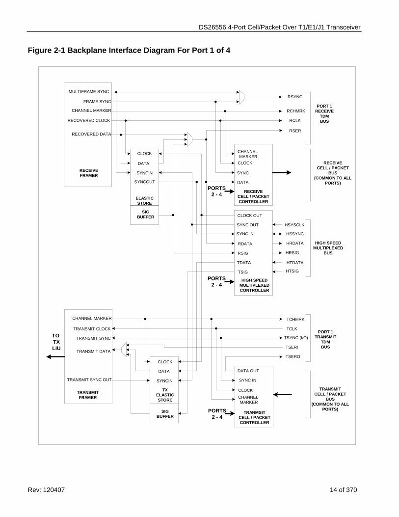
Figure 2-1 Backplane Interface Diagram For Port 1 of 4
RCLK
RSER
RCHMRK
SYNCIN
RECOVERED DATA
RECOVERED CLOCK
CHANNEL MARKER
RSYNC
SYNCOUT DATA
SYNC
CLOCK
CHANNEL MARKER
ELASTICSTORE
SIGBUFFER
HSYSCLK
HSSYNC
HRDATA
HTDATA
HRSIG
HTSIG
HIGH SPEEDMULTIPLEXED
BUS
RDATA
CLOCK OUT
RSIG
CHANNEL MARKER
CLOCK
SYNC IN
DATA OUT
CHANNEL MARKER
TSERI
TSERO
TCLK
TSYNC (I/O)
TCHMRK
TDATA
DATA
SYNC OUT
TXELASTICSTORE
SIGBUFFER
TRANSMIT CLOCK
TRANSMIT DATA
TRANSMIT SYNC
TRANSMIT SYNC OUT
CLOCK
DATA
SYNCIN
PORTS2 - 4
PORTS2 - 4
PORTS2 - 4
TSIG
MULTIFRAME SYNC
FRAME SYNC
RECEIVEFRAMER
SYNC IN
RECEIVECELL / PACKET
BUS(COMMON TO ALL
PORTS)
PORT 1RECEIVE
TDMBUS
RECEIVECELL / PACKETCONTROLLER
HIGH SPEEDMULTIPLEXEDCONTROLLER
PORT 1TRANSMIT
TDMBUS
TRANMSITCELL / PACKETCONTROLLER
TRANSMITCELL / PACKET
BUS(COMMON TO ALL
PORTS)
CLOCK
TRANSMITFRAMER
TO TX LIU
DS26556 4-Port Cell/Packet Over T1/E1/J1 Transceiver
Rev: 120407 15 of 370
3 BACKPLANE CONFIGURATION SCENARIOS
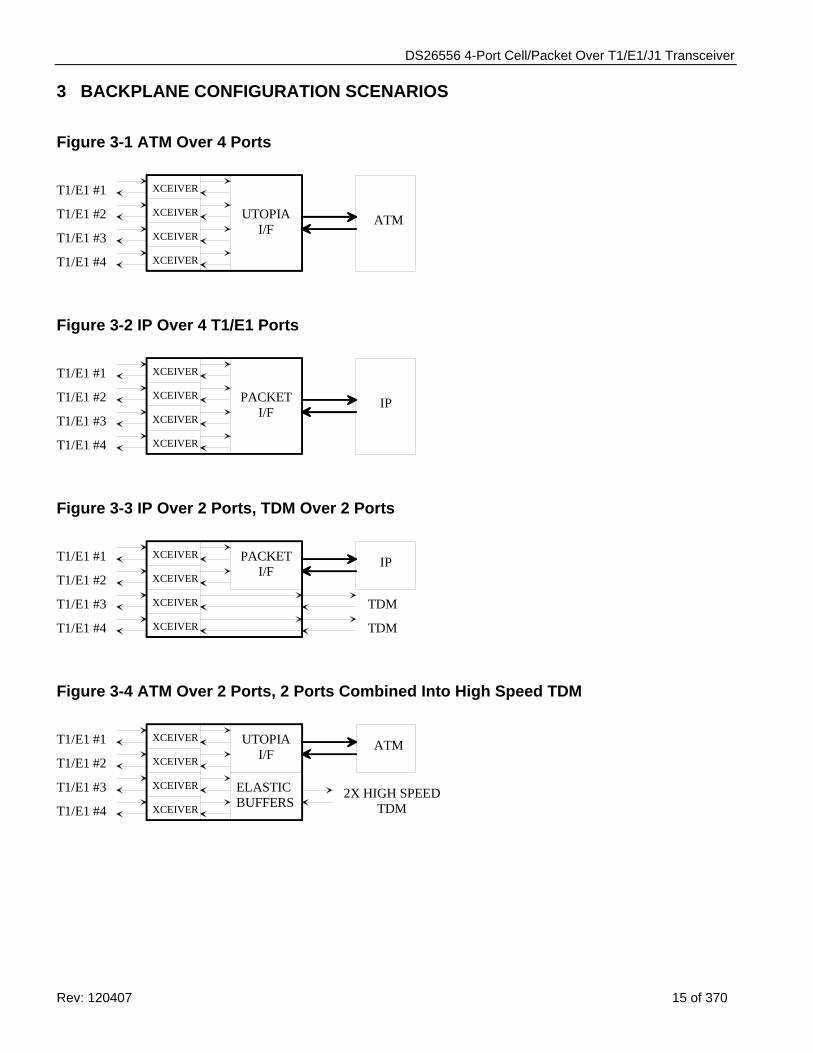
Figure 3-1 ATM Over 4 Ports
UTOPIAI/F
XCEIVER
XCEIVER
XCEIVER
XCEIVER
ATM
T1/E1 #1
T1/E1 #2
T1/E1 #3
T1/E1 #4
Figure 3-2 IP Over 4 T1/E1 Ports
PACKETI/F
XCEIVER
XCEIVER
XCEIVER
XCEIVER
IP
T1/E1 #1
T1/E1 #2
T1/E1 #3
T1/E1 #4
Figure 3-3 IP Over 2 Ports, TDM Over 2 Ports
PACKETI/F
XCEIVER
XCEIVER
XCEIVER
XCEIVER
IPT1/E1 #1
T1/E1 #2
T1/E1 #3
T1/E1 #4
TDM
TDM
Figure 3-4 ATM Over 2 Ports, 2 Ports Combined Into High Speed TDM
UTOPIAI/F
XCEIVER
XCEIVER
XCEIVER
XCEIVER
ATMT1/E1 #1
T1/E1 #2
T1/E1 #3
T1/E1 #42X HIGH SPEED
TDMELASTICBUFFERS
DS26556 4-Port Cell/Packet Over T1/E1/J1 Transceiver
Rev: 120407 16 of 370
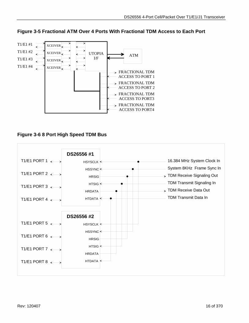
Figure 3-5 Fractional ATM Over 4 Ports With Fractional TDM Access to Each Port
UTOPIAI/F
XCEIVER
XCEIVER
XCEIVER
XCEIVER
ATM
T1/E1 #1
T1/E1 #2
T1/E1 #3
T1/E1 #4FRACTIONAL TDMACCESS TO PORT 1FRACTIONAL TDMACCESS TO PORT 2FRACTIONAL TDMACCESS TO PORT3FRACTIONAL TDMACCESS TO PORT4
Figure 3-6 8 Port High Speed TDM Bus
HSYSCLK
HSSYNC
HRSIG
HRDATA
16.384 MHz System Clock In
System 8KHz Frame Sync In
TDM Receive Data Out
TDM Transmit Data In
TDM Receive Signaling Out
TDM Transmit Signaling InHTSIG
HTDATA
HSYSCLK
HSSYNC
HRSIG
HRDATA
HTSIG
HTDATA
DS26556 #2
DS26556 #1T1/E1 PORT 1
T1/E1 PORT 2
T1/E1 PORT 3
T1/E1 PORT 4
T1/E1 PORT 5
T1/E1 PORT 6
T1/E1 PORT 7
T1/E1 PORT 8
DS26556 4-Port Cell/Packet Over T1/E1/J1 Transceiver
Rev: 120407 17 of 370
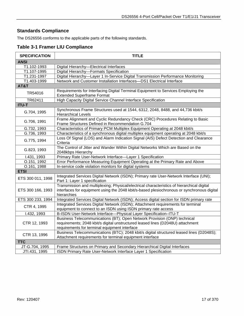
Standards Compliance The DS26556 conforms to the applicable parts of the following standards.
Table 3-1 Framer LIU Compliance
SPECIFICATION TITLE ANSI
T1.102-1993 Digital Hierarchy—Electrical Interfaces T1.107-1995 Digital Hierarchy—Formats Specification T1.231-1997 Digital Hierarchy—Layer 1 In-Service Digital Transmission Performance Monitoring T1.403-1999 Network and Customer Installation Interfaces—DS1 Electrical Interface
AT&T
TR54016 Requirements for Interfacing Digital Terminal Equipment to Services Employing the Extended Superframe Format
TR62411 High Capacity Digital Service Channel Interface Specification ITU-T
G.704, 1995 Synchronous Frame Structures used at 1544, 6312, 2048, 8488, and 44,736 kbit/s Hierarchical Levels
G.706, 1991 Frame Alignment and Cyclic Redundancy Check (CRC) Procedures Relating to Basic Frame Structures Defined in Recommendation G.704
G.732, 1993 Characteristics of Primary PCM Multiplex Equipment Operating at 2048 kbit/s G.736, 1993 Characteristics of a synchronous digital multiplex equipment operating at 2048 kbit/s
G.775, 1994 Loss Of Signal (LOS) and Alarm Indication Signal (AIS) Defect Detection and Clearance Criteria
G.823, 1993 The Control of Jitter and Wander Within Digital Networks Which are Based on the 2048kbps Hierarchy
I.431, 1993 Primary Rate User-Network Interface—Layer 1 Specification O.151, 1992 Error Performance Measuring Equipment Operating at the Primary Rate and Above O.161, 1988 In-service code violation monitors for digital systems
ETSI
ETS 300 011, 1998 Integrated Services Digital Network (ISDN); Primary rate User-Network Interface (UNI); Part 1: Layer 1 specification
ETS 300 166, 1993 Transmission and multiplexing; Physical/electrical characteristics of hierarchical digital interfaces for equipment using the 2048 kbit/s-based plesiochronous or synchronous digital hierarchies
ETS 300 233, 1994 Integrated Services Digital Network (ISDN); Access digital section for ISDN primary rate
CTR 4, 1995 Integrated Services Digital Network (ISDN); Attachment requirements for terminal equipment to connect to an ISDN using ISDN primary rate access
I.432, 1993 B-ISDN User-Network Interface—Physical Layer Specification–ITU-T
CTR 12, 1993 Business Telecommunications (BT); Open Network Provision (ONP) technical requirements; 2048 kbit/s digital unstructured leased lines (D2048U) attachment requirements for terminal equipment interface
CTR 13, 1996 Business Telecommunications (BTC); 2048 kbit/s digital structured leased lines (D2048S); Attachment requirements for terminal equipment interface
TTC JT-G.704, 1995 Frame Structures on Primary and Secondary Hierarchical Digital Interfaces JTI.431, 1995 ISDN Primary Rate User-Network Interface Layer 1 Specification
DS26556 4-Port Cell/Packet Over T1/E1/J1 Transceiver
Rev: 120407 18 of 370
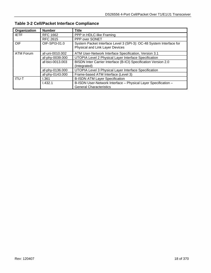
Table 3-2 Cell/Packet Interface Compliance Organization Number Title IETF RFC 1662 PPP in HDLC-like Framing RFC 2615 PPP over SONET OIF OIF-SPI3-01.0 System Packet Interface Level 3 (SPI-3): OC-48 System Interface for
Physical and Link Layer Devices
ATM Forum af-uni-0010.002 ATM User-Network Interface Specification, Version 3.1 af-phy-0039.000 UTOPIA Level 2 Physical Layer Interface Specification af-bici-0013.003 BISDN Inter Carrier Interface (B-ICI) Specification Version 2.0
(Integrated) af-phy-0136.000 UTOPIA Level 3 Physical Layer Interface Specification af-phy-0143.000 Frame-based ATM Interface (Level 3) ITU-T I.361 B-ISDN ATM Layer Specification I.432.1 B-ISDN User-Network Interface – Physical Layer Specification –
General Characteristics
DS26556 4-Port Cell/Packet Over T1/E1/J1 Transceiver
Rev: 120407 19 of 370
4 ACRONYMS AND GLOSSARY Definition of the terms used in this data sheet:
Acronyms • ATM – Asynchronous Transfer Mode • CC52 – Clear Channel 52 Mbps (STS-1 Clock Rate) • CLAD – Clock Rate Adapter • CLR – Clear Channel Mode • DSS – Distributed Sample Scrambler • FFRAC – Flexible Fractional Mode • FRM – Frame Mode • HDLC – High Level Data Link Control • SPI-3 – same as POS-PHY L3 • TDM – Time Division Multiplexing Glossary • Cell – ATM cell • Clear Channel – A data stream with no framing included • Fractional – Uses only a portion of available payload for data, also known as subrate • Octet Aligned – Byte aligned • Packet – HDLC packet • Subrate – See Fractional
DS26556 4-Port Cell/Packet Over T1/E1/J1 Transceiver
Rev: 120407 20 of 370
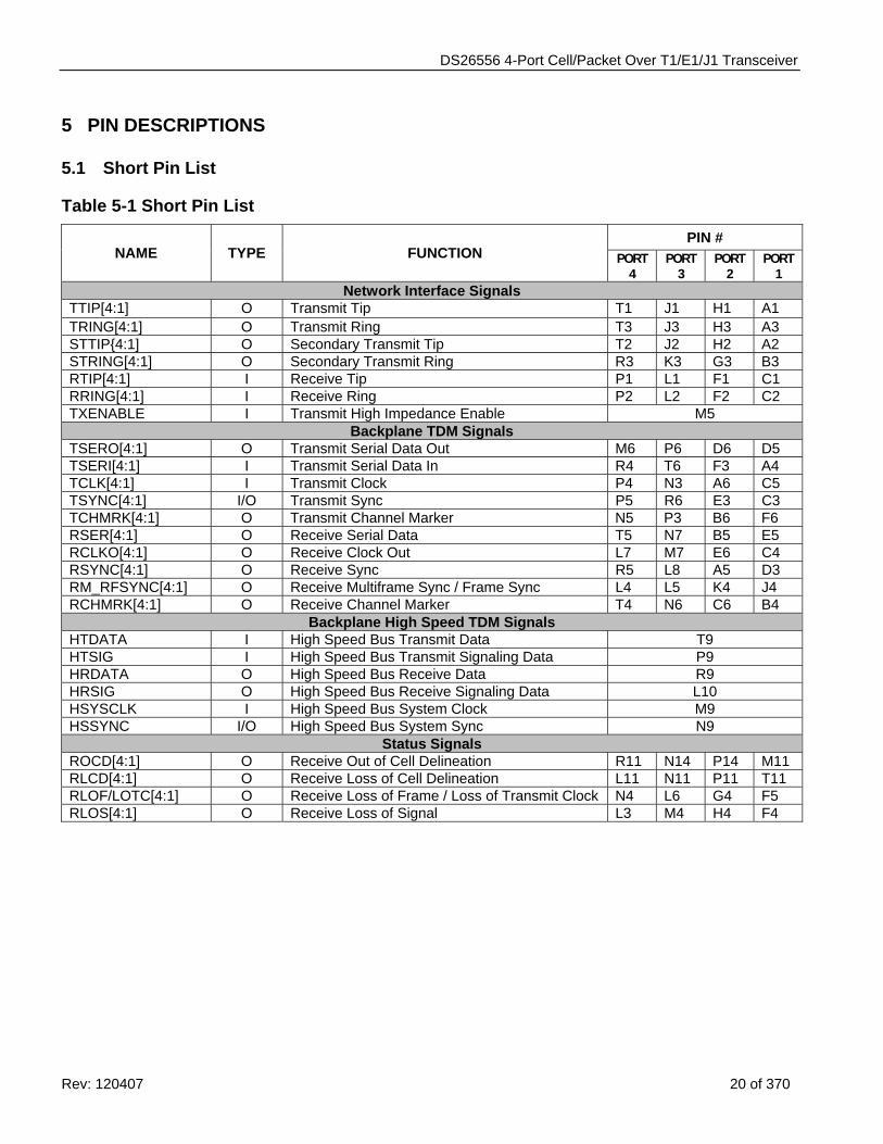
5 PIN DESCRIPTIONS
5.1 Short Pin List
Table 5-1 Short Pin List
PIN # NAME TYPE FUNCTION PORT
4 PORT
3 PORT
2 PORT
1 Network Interface Signals
TTIP[4:1] O Transmit Tip T1 J1 H1 A1 TRING[4:1] O Transmit Ring T3 J3 H3 A3 STTIP{4:1] O Secondary Transmit Tip T2 J2 H2 A2 STRING[4:1] O Secondary Transmit Ring R3 K3 G3 B3 RTIP[4:1] I Receive Tip P1 L1 F1 C1 RRING[4:1] I Receive Ring P2 L2 F2 C2 TXENABLE I Transmit High Impedance Enable M5
Backplane TDM Signals TSERO[4:1] O Transmit Serial Data Out M6 P6 D6 D5 TSERI[4:1] I Transmit Serial Data In R4 T6 F3 A4 TCLK[4:1] I Transmit Clock P4 N3 A6 C5 TSYNC[4:1] I/O Transmit Sync P5 R6 E3 C3 TCHMRK[4:1] O Transmit Channel Marker N5 P3 B6 F6 RSER[4:1] O Receive Serial Data T5 N7 B5 E5 RCLKO[4:1] O Receive Clock Out L7 M7 E6 C4 RSYNC[4:1] O Receive Sync R5 L8 A5 D3 RM_RFSYNC[4:1] O Receive Multiframe Sync / Frame Sync L4 L5 K4 J4 RCHMRK[4:1] O Receive Channel Marker T4 N6 C6 B4
Backplane High Speed TDM Signals HTDATA I High Speed Bus Transmit Data T9 HTSIG I High Speed Bus Transmit Signaling Data P9 HRDATA O High Speed Bus Receive Data R9 HRSIG O High Speed Bus Receive Signaling Data L10 HSYSCLK I High Speed Bus System Clock M9 HSSYNC I/O High Speed Bus System Sync N9
Status Signals ROCD[4:1] O Receive Out of Cell Delineation R11 N14 P14 M11 RLCD[4:1] O Receive Loss of Cell Delineation L11 N11 P11 T11 RLOF/LOTC[4:1] O Receive Loss of Frame / Loss of Transmit Clock N4 L6 G4 F5 RLOS[4:1] O Receive Loss of Signal L3 M4 H4 F4
DS26556 4-Port Cell/Packet Over T1/E1/J1 Transceiver
Rev: 120407 21 of 370
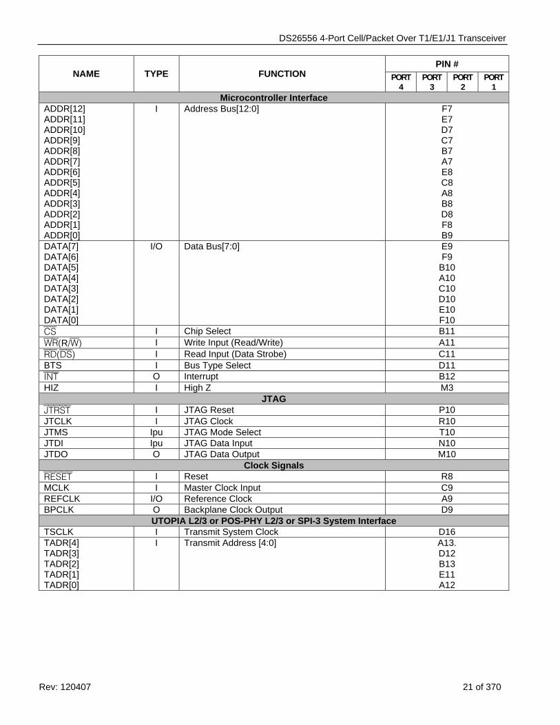
PIN # NAME TYPE FUNCTION PORT
4 PORT
3 PORT
2 PORT
1 Microcontroller Interface
ADDR[12] ADDR[11] ADDR[10] ADDR[9] ADDR[8] ADDR[7] ADDR[6] ADDR[5] ADDR[4] ADDR[3] ADDR[2] ADDR[1] ADDR[0]
I Address Bus[12:0] F7 E7 D7 C7 B7 A7 E8 C8 A8 B8 D8 F8 B9
DATA[7] DATA[6] DATA[5] DATA[4] DATA[3] DATA[2] DATA[1] DATA[0]
I/O Data Bus[7:0] E9 F9
B10 A10 C10 D10 E10 F10
CS I Chip Select B11 WR(R/W) I Write Input (Read/Write) A11 RD(DS) I Read Input (Data Strobe) C11 BTS I Bus Type Select D11 INT O Interrupt B12 HIZ I High Z M3
JTAG JTRST I JTAG Reset P10 JTCLK I JTAG Clock R10 JTMS Ipu JTAG Mode Select T10 JTDI Ipu JTAG Data Input N10 JTDO O JTAG Data Output M10
Clock Signals RESET I Reset R8 MCLK I Master Clock Input C9 REFCLK I/O Reference Clock A9 BPCLK O Backplane Clock Output D9
UTOPIA L2/3 or POS-PHY L2/3 or SPI-3 System Interface TSCLK I Transmit System Clock D16 TADR[4] TADR[3] TADR[2] TADR[1] TADR[0]
I Transmit Address [4:0] A13. D12 B13 E11 A12
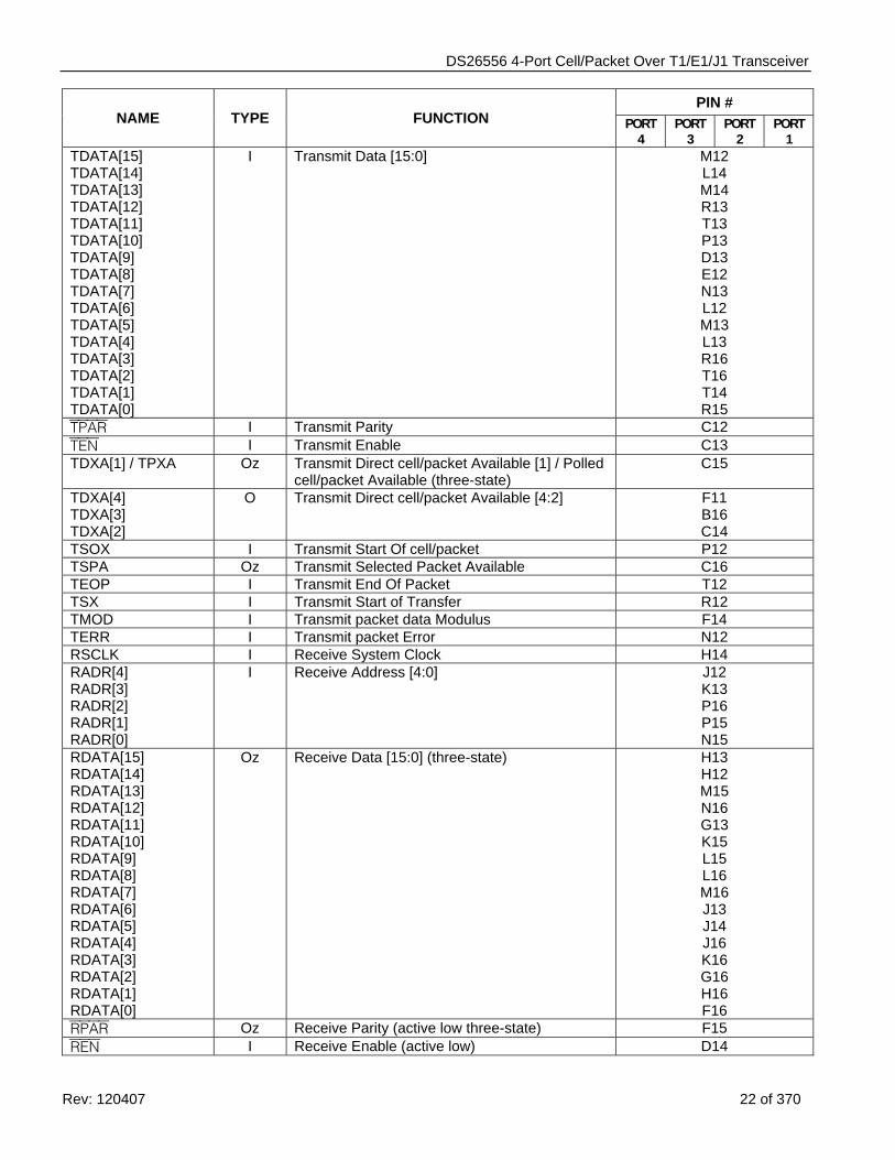
DS26556 4-Port Cell/Packet Over T1/E1/J1 Transceiver
Rev: 120407 22 of 370
PIN # NAME TYPE FUNCTION PORT
4 PORT
3 PORT
2 PORT
1 TDATA[15] TDATA[14] TDATA[13] TDATA[12] TDATA[11] TDATA[10] TDATA[9] TDATA[8] TDATA[7] TDATA[6] TDATA[5] TDATA[4] TDATA[3] TDATA[2] TDATA[1] TDATA[0]
I Transmit Data [15:0] M12 L14 M14 R13 T13 P13 D13 E12 N13 L12 M13 L13 R16 T16 T14 R15
TPAR I Transmit Parity C12 TEN I Transmit Enable C13 TDXA[1] / TPXA Oz Transmit Direct cell/packet Available [1] / Polled
cell/packet Available (three-state) C15
TDXA[4] TDXA[3] TDXA[2]
O Transmit Direct cell/packet Available [4:2] F11 B16 C14
TSOX I Transmit Start Of cell/packet P12 TSPA Oz Transmit Selected Packet Available C16 TEOP I Transmit End Of Packet T12 TSX I Transmit Start of Transfer R12 TMOD I Transmit packet data Modulus F14 TERR I Transmit packet Error N12 RSCLK I Receive System Clock H14 RADR[4] RADR[3] RADR[2] RADR[1] RADR[0]
I Receive Address [4:0] J12 K13 P16 P15 N15
RDATA[15] RDATA[14] RDATA[13] RDATA[12] RDATA[11] RDATA[10] RDATA[9] RDATA[8] RDATA[7] RDATA[6] RDATA[5] RDATA[4] RDATA[3] RDATA[2] RDATA[1] RDATA[0]
Oz Receive Data [15:0] (three-state) H13 H12 M15 N16 G13 K15 L15 L16 M16 J13 J14 J16 K16 G16 H16 F16
RPAR Oz Receive Parity (active low three-state) F15 REN I Receive Enable (active low) D14
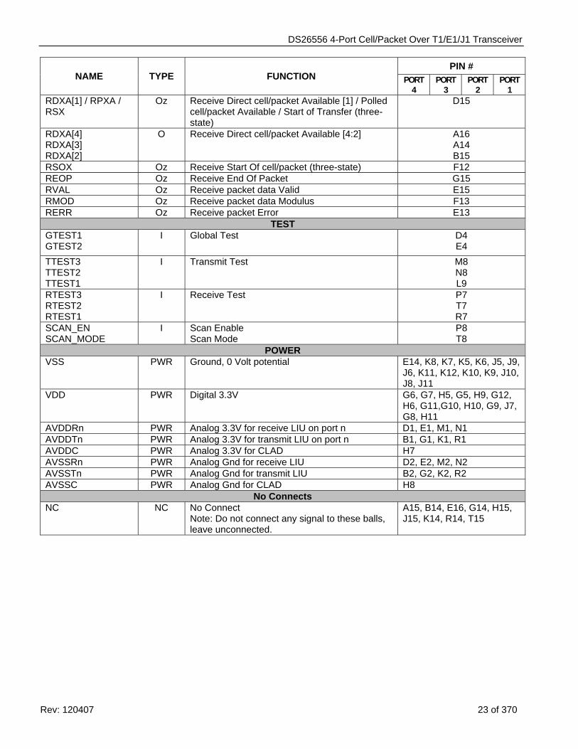
DS26556 4-Port Cell/Packet Over T1/E1/J1 Transceiver
Rev: 120407 23 of 370
PIN # NAME TYPE FUNCTION PORT
4 PORT
3 PORT
2 PORT
1 RDXA[1] / RPXA / RSX
Oz Receive Direct cell/packet Available [1] / Polled cell/packet Available / Start of Transfer (three-state)
D15
RDXA[4] RDXA[3] RDXA[2]
O Receive Direct cell/packet Available [4:2] A16 A14 B15
RSOX Oz Receive Start Of cell/packet (three-state) F12 REOP Oz Receive End Of Packet G15 RVAL Oz Receive packet data Valid E15 RMOD Oz Receive packet data Modulus F13 RERR Oz Receive packet Error E13
TEST GTEST1 GTEST2
I Global Test D4 E4
TTEST3 TTEST2 TTEST1
I Transmit Test M8 N8 L9
RTEST3 RTEST2 RTEST1
I Receive Test P7 T7 R7
SCAN_EN SCAN_MODE
I Scan Enable Scan Mode
P8 T8
POWER VSS PWR Ground, 0 Volt potential E14, K8, K7, K5, K6, J5, J9,
J6, K11, K12, K10, K9, J10, J8, J11
VDD PWR Digital 3.3V G6, G7, H5, G5, H9, G12, H6, G11,G10, H10, G9, J7, G8, H11
AVDDRn PWR Analog 3.3V for receive LIU on port n D1, E1, M1, N1 AVDDTn PWR Analog 3.3V for transmit LIU on port n B1, G1, K1, R1 AVDDC PWR Analog 3.3V for CLAD H7 AVSSRn PWR Analog Gnd for receive LIU D2, E2, M2, N2 AVSSTn PWR Analog Gnd for transmit LIU B2, G2, K2, R2 AVSSC PWR Analog Gnd for CLAD H8
No Connects NC NC No Connect
Note: Do not connect any signal to these balls, leave unconnected.
A15, B14, E16, G14, H15, J15, K14, R14, T15
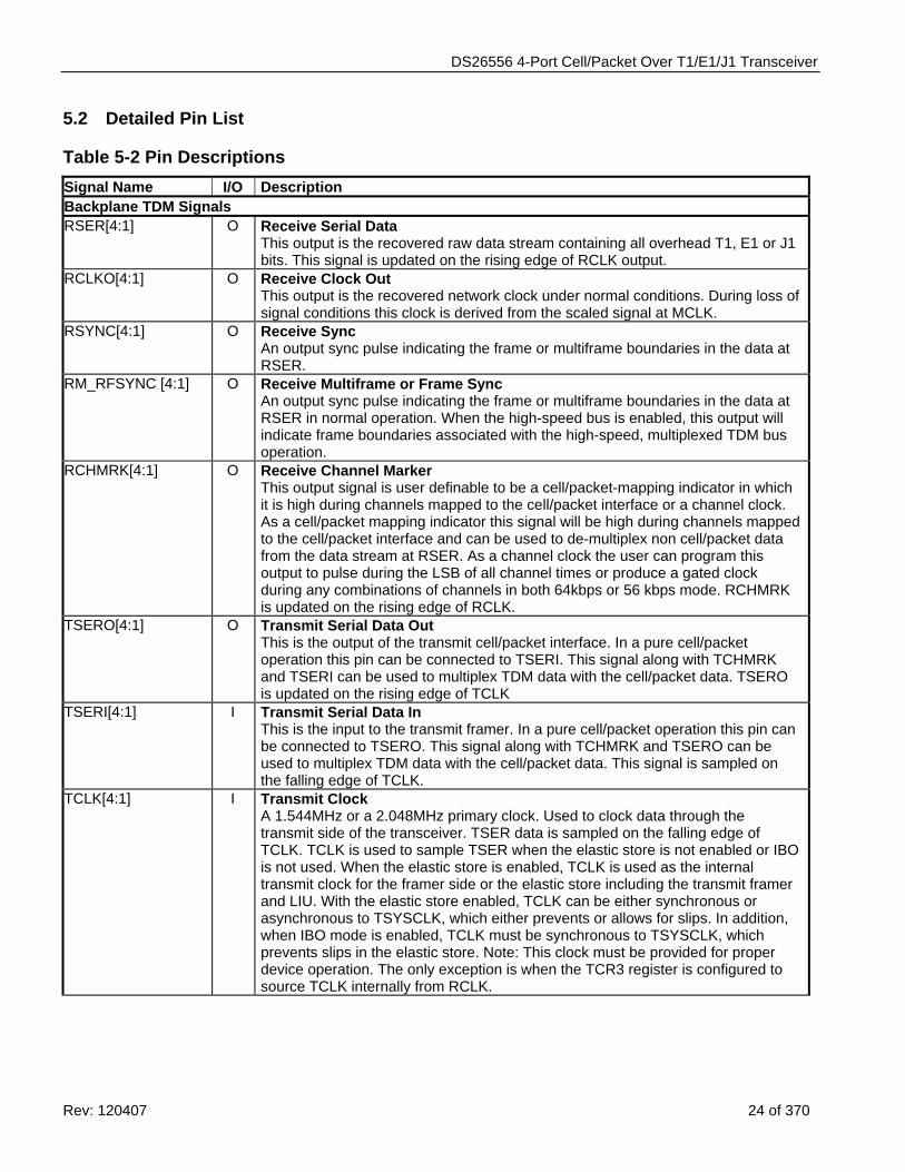
DS26556 4-Port Cell/Packet Over T1/E1/J1 Transceiver
Rev: 120407 24 of 370
5.2 Detailed Pin List
Table 5-2 Pin Descriptions Signal Name I/O Description Backplane TDM Signals RSER[4:1] O Receive Serial Data
This output is the recovered raw data stream containing all overhead T1, E1 or J1 bits. This signal is updated on the rising edge of RCLK output.
RCLKO[4:1] O Receive Clock Out This output is the recovered network clock under normal conditions. During loss of signal conditions this clock is derived from the scaled signal at MCLK.
RSYNC[4:1] O Receive Sync An output sync pulse indicating the frame or multiframe boundaries in the data at RSER.
RM_RFSYNC [4:1] O Receive Multiframe or Frame Sync An output sync pulse indicating the frame or multiframe boundaries in the data at RSER in normal operation. When the high-speed bus is enabled, this output will indicate frame boundaries associated with the high-speed, multiplexed TDM bus operation.
RCHMRK[4:1] O Receive Channel Marker This output signal is user definable to be a cell/packet-mapping indicator in which it is high during channels mapped to the cell/packet interface or a channel clock. As a cell/packet mapping indicator this signal will be high during channels mapped to the cell/packet interface and can be used to de-multiplex non cell/packet data from the data stream at RSER. As a channel clock the user can program this output to pulse during the LSB of all channel times or produce a gated clock during any combinations of channels in both 64kbps or 56 kbps mode. RCHMRK is updated on the rising edge of RCLK.
TSERO[4:1] O Transmit Serial Data Out This is the output of the transmit cell/packet interface. In a pure cell/packet operation this pin can be connected to TSERI. This signal along with TCHMRK and TSERI can be used to multiplex TDM data with the cell/packet data. TSERO is updated on the rising edge of TCLK
TSERI[4:1] I Transmit Serial Data In This is the input to the transmit framer. In a pure cell/packet operation this pin can be connected to TSERO. This signal along with TCHMRK and TSERO can be used to multiplex TDM data with the cell/packet data. This signal is sampled on the falling edge of TCLK.
TCLK[4:1] I Transmit Clock A 1.544MHz or a 2.048MHz primary clock. Used to clock data through the transmit side of the transceiver. TSER data is sampled on the falling edge of TCLK. TCLK is used to sample TSER when the elastic store is not enabled or IBO is not used. When the elastic store is enabled, TCLK is used as the internal transmit clock for the framer side or the elastic store including the transmit framer and LIU. With the elastic store enabled, TCLK can be either synchronous or asynchronous to TSYSCLK, which either prevents or allows for slips. In addition, when IBO mode is enabled, TCLK must be synchronous to TSYSCLK, which prevents slips in the elastic store. Note: This clock must be provided for proper device operation. The only exception is when the TCR3 register is configured to source TCLK internally from RCLK.
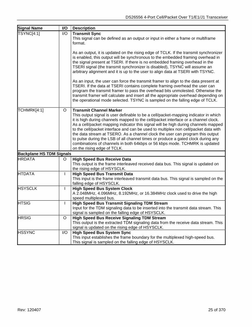
DS26556 4-Port Cell/Packet Over T1/E1/J1 Transceiver
Rev: 120407 25 of 370
Signal Name I/O Description TSYNC[4:1] I/O Transmit Sync
This signal can be defined as an output or input in either a frame or multiframe format. As an output, it is updated on the rising edge of TCLK. If the transmit synchronizer is enabled, this output will be synchronous to the embedded framing overhead in the signal present at TSERI. If there is no embedded framing overhead in the TSERI signal (the transmit synchronizer is disabled), TSYNC will assume an arbitrary alignment and it is up to the user to align data at TSERI with TSYNC. As an input, the user can force the transmit framer to align to the data present at TSERI. If the data at TSERI contains complete framing overhead the user can program the transmit framer to pass the overhead bits unmolested. Otherwise the transmit framer will calculate and insert all the appropriate overhead depending on the operational mode selected. TSYNC is sampled on the falling edge of TCLK.
TCHMRK[4:1] O Transmit Channel Marker This output signal is user definable to be a cell/packet-mapping indicator in which it is high during channels mapped to the cell/packet interface or a channel clock. As a cell/packet mapping indicator this signal will be high during channels mapped to the cell/packet interface and can be used to multiplex non cell/packet data with the data stream at TSERO. As a channel clock the user can program this output to pulse during the LSB of all channel times or produce a gated clock during any combinations of channels in both 64kbps or 56 kbps mode. TCHMRK is updated on the rising edge of TCLK.
Backplane HS TDM Signals HRDATA O High Speed Bus Receive Data
This output is the frame interleaved received data bus. This signal is updated on the rising edge of HSYSCLK.
HTDATA I High Speed Bus Transmit Data This input is the frame interleaved transmit data bus. This signal is sampled on the falling edge of HSYSCLK.
HSYSCLK I High Speed Bus System Clock A 2.048MHz, 4.096MHz, 8.192MHz, or 16.384MHz clock used to drive the high speed multiplexed bus.
HTSIG I High Speed Bus Transmit Signaling TDM Stream Input for the TDM signaling data to be inserted into the transmit data stream. This signal is sampled on the falling edge of HSYSCLK.
HRSIG O High Speed Bus Receive Signaling TDM Stream This output is the extracted TDM signaling data from the receive data stream. This signal is updated on the rising edge of HSYSCLK.
HSSYNC I/O High Speed Bus System Sync This input establishes the frame boundary for the multiplexed high-speed bus. This signal is sampled on the falling edge of HSYSCLK.
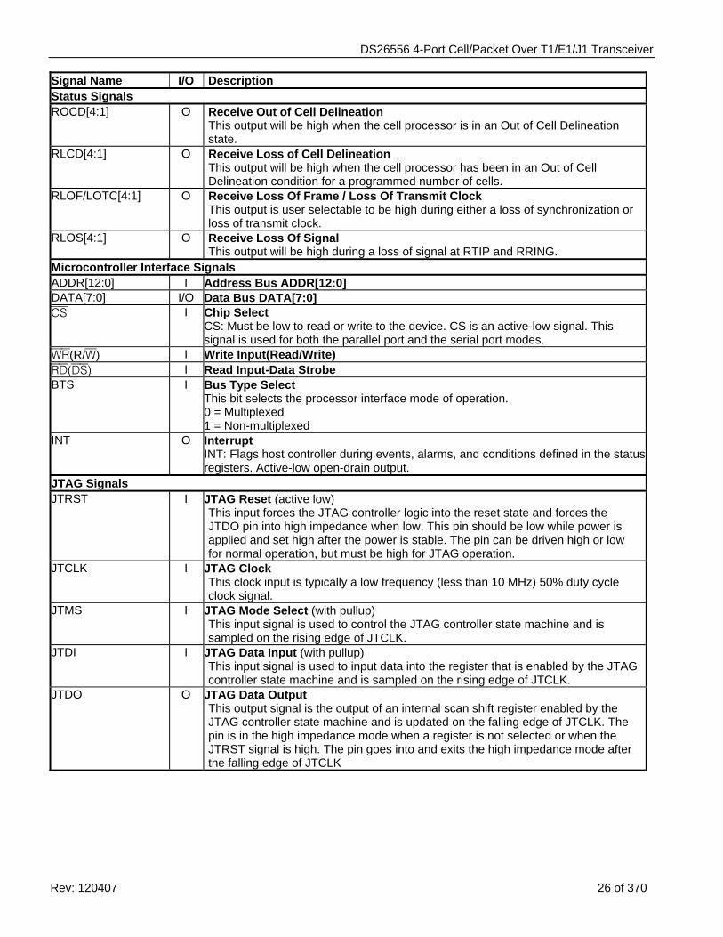
DS26556 4-Port Cell/Packet Over T1/E1/J1 Transceiver
Rev: 120407 26 of 370
Signal Name I/O Description Status Signals ROCD[4:1] O Receive Out of Cell Delineation
This output will be high when the cell processor is in an Out of Cell Delineation state.
RLCD[4:1] O Receive Loss of Cell Delineation This output will be high when the cell processor has been in an Out of Cell Delineation condition for a programmed number of cells.
RLOF/LOTC[4:1] O Receive Loss Of Frame / Loss Of Transmit Clock This output is user selectable to be high during either a loss of synchronization or loss of transmit clock.
RLOS[4:1] O Receive Loss Of Signal This output will be high during a loss of signal at RTIP and RRING.
Microcontroller Interface Signals ADDR[12:0] I Address Bus ADDR[12:0] DATA[7:0] I/O Data Bus DATA[7:0] CS I Chip Select
CS: Must be low to read or write to the device. CS is an active-low signal. This signal is used for both the parallel port and the serial port modes.
WR(R/W) I Write Input(Read/Write) RD(DS) I Read Input-Data Strobe BTS I Bus Type Select
This bit selects the processor interface mode of operation. 0 = Multiplexed 1 = Non-multiplexed
INT O Interrupt INT: Flags host controller during events, alarms, and conditions defined in the status registers. Active-low open-drain output.
JTAG Signals JTRST I JTAG Reset (active low)
This input forces the JTAG controller logic into the reset state and forces the JTDO pin into high impedance when low. This pin should be low while power is applied and set high after the power is stable. The pin can be driven high or low for normal operation, but must be high for JTAG operation.
JTCLK I JTAG Clock This clock input is typically a low frequency (less than 10 MHz) 50% duty cycle clock signal.
JTMS I JTAG Mode Select (with pullup) This input signal is used to control the JTAG controller state machine and is sampled on the rising edge of JTCLK.
JTDI I JTAG Data Input (with pullup) This input signal is used to input data into the register that is enabled by the JTAG controller state machine and is sampled on the rising edge of JTCLK.
JTDO O JTAG Data Output This output signal is the output of an internal scan shift register enabled by the JTAG controller state machine and is updated on the falling edge of JTCLK. The pin is in the high impedance mode when a register is not selected or when the JTRST signal is high. The pin goes into and exits the high impedance mode after the falling edge of JTCLK
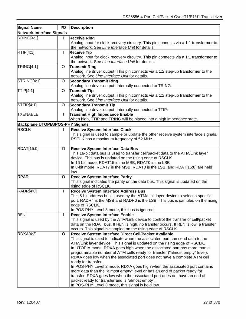
DS26556 4-Port Cell/Packet Over T1/E1/J1 Transceiver
Rev: 120407 27 of 370
Signal Name I/O Description Network Interface Signals RRING[4:1] I Receive Ring
Analog input for clock recovery circuitry. This pin connects via a 1:1 transformer to the network. See Line Interface Unit for details.
RTIP[4:1] I Receive Tip Analog input for clock recovery circuitry. This pin connects via a 1:1 transformer to the network. See Line Interface Unit for details.
TRING[4:1] O Transmit Ring Analog line driver output. This pin connects via a 1:2 step-up transformer to the network. See Line Interface Unit for details.
STRING[4:1] O Secondary Transmit Ring Analog line driver output. Internally connected to TRING.
TTIP[4:1] O Transmit Tip Analog line driver output. This pin connects via a 1:2 step-up transformer to the network. See Line Interface Unit for details.
STTIP[4:1] O Secondary Transmit Tip Analog line driver output. Internally connected to TTIP.
TXENABLE I Transmit High Impedance Enable When high, TTIP and TRING will be placed into a high impedance state.
Backplane UTOPIA/POS-PHY Signals RSCLK I Receive System Interface Clock
This signal is used to sample or update the other receive system interface signals. RSCLK has a maximum frequency of 52 MHz.
RDAT[15:0] O Receive System Interface Data Bus
This 16-bit data bus is used to transfer cell/packet data to the ATM/Link layer device. This bus is updated on the rising edge of RSCLK. In 16-bit mode, RDAT15 is the MSB, RDAT0 is the LSB In 8-bit mode, RDAT7 is the MSB, RDAT0 is the LSB, and RDAT[15:8] are held low.
RPAR O Receive System Interface Parity This signal indicates the parity on the data bus. This signal is updated on the rising edge of RSCLK.
RADR[4:0] I Receive System Interface Address Bus This 5-bit address bus is used by the ATM/Link layer device to select a specific port. RADR4 is the MSB and RADR0 is the LSB. This bus is sampled on the rising edge of RSCLK. In POS-PHY Level 3 mode, this bus is ignored.
REN I Receive System Interface Enable This signal is used by the ATM/Link device to control the transfer of cell/packet data on the RDAT bus. If REN is high, no transfer occurs. If REN is low, a transfer occurs. This signal is sampled on the rising edge of RSCLK.
RDXA[4:2] O Receive System Interface Direct Cell/Packet Available This signal is used to indicate when the associated port can send data to the ATM/Link layer device. This signal is updated on the rising edge of RSCLK. In UTOPIA mode, RDXA goes high when the associated port has more than a programmable number of ATM cells ready for transfer ("almost empty" level). RDXA goes low when the associated port does not have a complete ATM cell ready for transfer. In POS-PHY Level 2 mode, RDXA goes high when the associated port contains more data than the "almost empty" level or has an end of packet ready for transfer. RDXA goes low when the associated port does not have an end of packet ready for transfer and is "almost empty". In POS-PHY Level 3 mode, this signal is held low.
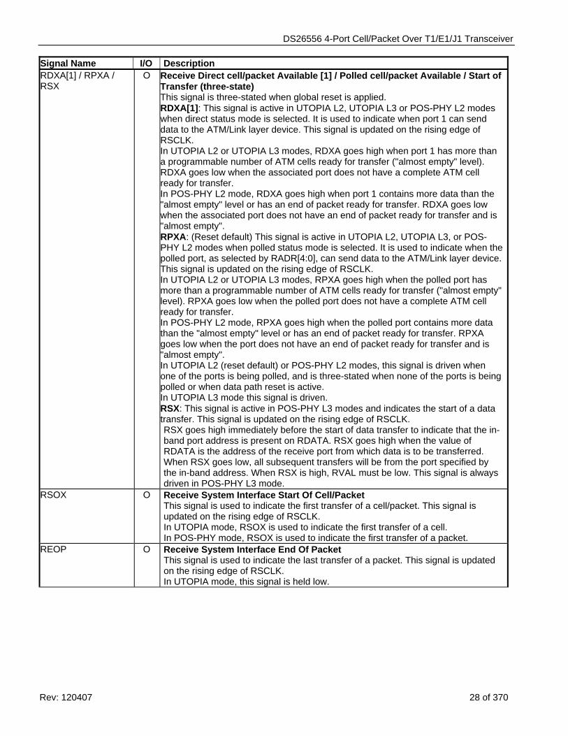
DS26556 4-Port Cell/Packet Over T1/E1/J1 Transceiver
Rev: 120407 28 of 370
Signal Name I/O Description RDXA[1] / RPXA / RSX
O Receive Direct cell/packet Available [1] / Polled cell/packet Available / Start of Transfer (three-state) This signal is three-stated when global reset is applied. RDXA[1]: This signal is active in UTOPIA L2, UTOPIA L3 or POS-PHY L2 modes when direct status mode is selected. It is used to indicate when port 1 can send data to the ATM/Link layer device. This signal is updated on the rising edge of RSCLK. In UTOPIA L2 or UTOPIA L3 modes, RDXA goes high when port 1 has more than a programmable number of ATM cells ready for transfer ("almost empty" level). RDXA goes low when the associated port does not have a complete ATM cell ready for transfer. In POS-PHY L2 mode, RDXA goes high when port 1 contains more data than the "almost empty" level or has an end of packet ready for transfer. RDXA goes low when the associated port does not have an end of packet ready for transfer and is "almost empty". RPXA: (Reset default) This signal is active in UTOPIA L2, UTOPIA L3, or POS-PHY L2 modes when polled status mode is selected. It is used to indicate when the polled port, as selected by RADR[4:0], can send data to the ATM/Link layer device. This signal is updated on the rising edge of RSCLK. In UTOPIA L2 or UTOPIA L3 modes, RPXA goes high when the polled port has more than a programmable number of ATM cells ready for transfer ("almost empty" level). RPXA goes low when the polled port does not have a complete ATM cell ready for transfer. In POS-PHY L2 mode, RPXA goes high when the polled port contains more data than the "almost empty" level or has an end of packet ready for transfer. RPXA goes low when the port does not have an end of packet ready for transfer and is "almost empty". In UTOPIA L2 (reset default) or POS-PHY L2 modes, this signal is driven when one of the ports is being polled, and is three-stated when none of the ports is being polled or when data path reset is active. In UTOPIA L3 mode this signal is driven. RSX: This signal is active in POS-PHY L3 modes and indicates the start of a data transfer. This signal is updated on the rising edge of RSCLK. RSX goes high immediately before the start of data transfer to indicate that the in-band port address is present on RDATA. RSX goes high when the value of RDATA is the address of the receive port from which data is to be transferred. When RSX goes low, all subsequent transfers will be from the port specified by the in-band address. When RSX is high, RVAL must be low. This signal is always driven in POS-PHY L3 mode.
RSOX O Receive System Interface Start Of Cell/Packet This signal is used to indicate the first transfer of a cell/packet. This signal is updated on the rising edge of RSCLK. In UTOPIA mode, RSOX is used to indicate the first transfer of a cell. In POS-PHY mode, RSOX is used to indicate the first transfer of a packet.
REOP O Receive System Interface End Of Packet This signal is used to indicate the last transfer of a packet. This signal is updated on the rising edge of RSCLK. In UTOPIA mode, this signal is held low.
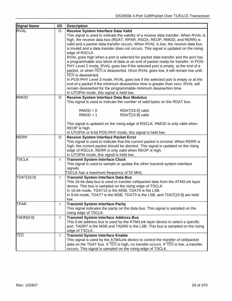
DS26556 4-Port Cell/Packet Over T1/E1/J1 Transceiver
Rev: 120407 29 of 370
Signal Name I/O Description RVAL O Receive System Interface Data Valid
This signal is used to indicate the validity of a receive data transfer. When RVAL is high, the receive data bus (RDAT, RPAR, RSOX, REOP, RMOD, and RERR) is valid and a packet data transfer occurs. When RVAL is low, the receive data bus is invalid and a data transfer does not occurs. This signal is updated on the rising edge of RSCLK. RVAL goes high when a port is selected for packet data transfer and the port has a programmable size block of data or an end of packet ready for transfer. In POS-PHY Level 2 mode, RVAL goes low if the selected port is empty, at the end of a packet, or when REN is deasserted. Once RVAL goes low, it will remain low until REN is deasserted. In POS-PHY Level 3 mode, RVAL goes low if the selected port is empty or at the end of a packet if the minimum deassertion time is greater than zero. RVAL will remain deasserted for the programmable minimum deassertion time. In UTOPIA mode, this signal is held low.
RMOD O Receive System Interface Data Bus Modulus This signal is used to indicate the number of valid bytes on the RDAT bus. RMOD = 0 RDAT[15:0] valid RMOD = 1 RDAT[15:8] valid This signal is updated on the rising edge of RSCLK. RMOD is only valid when REOP is high. In UTOPIA or 8-bit POS-PHY mode, this signal is held low.
RERR O Receive System Interface Packet Error This signal is used to indicate that the current packet is errored. When RERR is high, the current packet should be aborted. This signal is updated on the rising edge of RSCLK. RERR is only valid when REOP is high. In UTOPIA mode, this signal is held low.
TSCLK I Transmit System Interface Clock This signal is used to sample or update the other transmit system interface signals.
TSCLK has a maximum frequency of 52 MHz. TDAT[15:0] I Transmit System Interface Data Bus
This 16-bit data bus is used to transfer cell/packet data from the ATM/Link layer device. This bus is sampled on the rising edge of TSCLK. In 16-bit mode, TDAT15 is the MSB, TDAT0 is the LSB. In 8-bit mode, TDAT7 is the MSB, TDAT0 is the LSB, and TDAT[15:8] are held low.
TPAR I Transmit System Interface Parity This signal indicates the parity on the data bus. This signal is sampled on the rising edge of TSCLK.
TADR[4:0] I Transmit System Interface Address Bus This 5-bit address bus is used by the ATM/Link layer device to select a specific port. TADR7 is the MSB and TADR0 is the LSB. This bus is sampled on the rising edge of TSCLK.
TEN I Transmit System Interface Enable This signal is used by the ATM/Link device to control the transfer of cell/packet data on the TDAT bus. If TEN is high, no transfer occurs. If TEN is low, a transfer occurs. This signal is sampled on the rising edge of TSCLK.
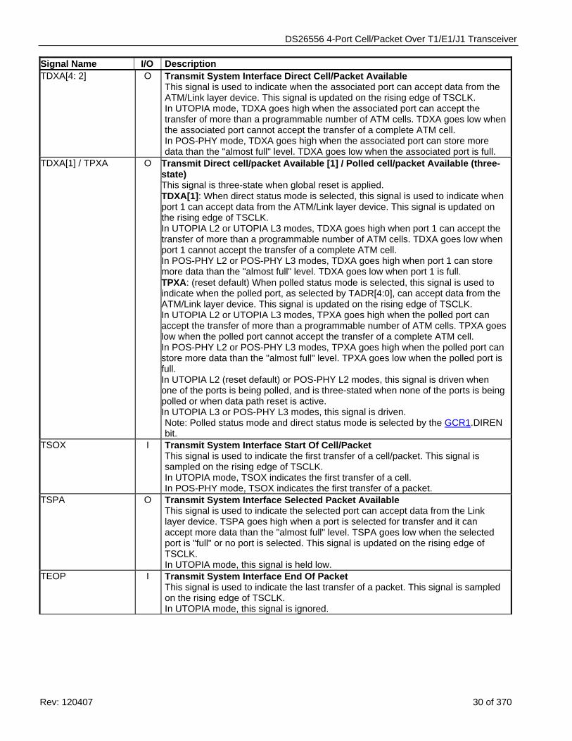
DS26556 4-Port Cell/Packet Over T1/E1/J1 Transceiver
Rev: 120407 30 of 370
Signal Name I/O Description TDXA[4: 2] O Transmit System Interface Direct Cell/Packet Available
This signal is used to indicate when the associated port can accept data from the ATM/Link layer device. This signal is updated on the rising edge of TSCLK. In UTOPIA mode, TDXA goes high when the associated port can accept the transfer of more than a programmable number of ATM cells. TDXA goes low when the associated port cannot accept the transfer of a complete ATM cell. In POS-PHY mode, TDXA goes high when the associated port can store more data than the "almost full" level. TDXA goes low when the associated port is full.
TDXA[1] / TPXA O Transmit Direct cell/packet Available [1] / Polled cell/packet Available (three-state) This signal is three-state when global reset is applied. TDXA[1]: When direct status mode is selected, this signal is used to indicate when port 1 can accept data from the ATM/Link layer device. This signal is updated on the rising edge of TSCLK. In UTOPIA L2 or UTOPIA L3 modes, TDXA goes high when port 1 can accept the transfer of more than a programmable number of ATM cells. TDXA goes low when port 1 cannot accept the transfer of a complete ATM cell. In POS-PHY L2 or POS-PHY L3 modes, TDXA goes high when port 1 can store more data than the "almost full" level. TDXA goes low when port 1 is full. TPXA: (reset default) When polled status mode is selected, this signal is used to indicate when the polled port, as selected by TADR[4:0], can accept data from the ATM/Link layer device. This signal is updated on the rising edge of TSCLK. In UTOPIA L2 or UTOPIA L3 modes, TPXA goes high when the polled port can accept the transfer of more than a programmable number of ATM cells. TPXA goes low when the polled port cannot accept the transfer of a complete ATM cell. In POS-PHY L2 or POS-PHY L3 modes, TPXA goes high when the polled port can store more data than the "almost full" level. TPXA goes low when the polled port is full. In UTOPIA L2 (reset default) or POS-PHY L2 modes, this signal is driven when one of the ports is being polled, and is three-stated when none of the ports is being polled or when data path reset is active. In UTOPIA L3 or POS-PHY L3 modes, this signal is driven. Note: Polled status mode and direct status mode is selected by the GCR1.DIREN bit.
TSOX I Transmit System Interface Start Of Cell/Packet This signal is used to indicate the first transfer of a cell/packet. This signal is sampled on the rising edge of TSCLK. In UTOPIA mode, TSOX indicates the first transfer of a cell. In POS-PHY mode, TSOX indicates the first transfer of a packet.
TSPA O Transmit System Interface Selected Packet Available This signal is used to indicate the selected port can accept data from the Link layer device. TSPA goes high when a port is selected for transfer and it can accept more data than the "almost full" level. TSPA goes low when the selected port is "full" or no port is selected. This signal is updated on the rising edge of TSCLK. In UTOPIA mode, this signal is held low.
TEOP I Transmit System Interface End Of Packet This signal is used to indicate the last transfer of a packet. This signal is sampled on the rising edge of TSCLK. In UTOPIA mode, this signal is ignored.
DS26556 4-Port Cell/Packet Over T1/E1/J1 Transceiver
Rev: 120407 31 of 370
Signal Name I/O Description TSX I Transmit System Interface Start of Transfer
This signal indicates the start of a data transfer. TSX goes high goes high immediately before the start of data transfer to indicate that the in-band port address is present on TDAT. TSX goes high when the value of TDAT is the address of the transmit port to which data is to be transferred. When TSX goes low, all subsequent transfers will be to the port specified by the in-band address. This signal is sampled on the rising edge of TSCLK. TSX is only valid when TEN is high. In UTOPIA or POS-PHY Level 2 mode, this signal is ignored.
TMOD I Transmit System Interface Data Bus Modulus This signal indicates the number of valid bytes on the TDAT bus. TMOD = 0 TDAT[15:0] valid TMOD = 1 TDAT[15:8] valid This signal is sampled on the rising edge of TSCLK. TMOD is only valid when TEOP is high. In UTOPIA or 8-bit POS-PHY mode, this signal is ignored.
TERR I Transmit System Interface Packet Error This signal indicates that the current packet is errored. When TERR is high, the current packet should be aborted. This signal is sampled on the rising edge of TSCLK. TERR is only valid when TEOP is high. In UTOPIA mode, this signal is ignored.
Clock Signals RESET I Reset (active low)
This signal resets all the internal processor registers and logic when low. This pin should be low while power is applied and set high after the power is stable. This is an asynchronous input.
MCLK I Master Clock Input A (50ppm) clock source. This clock is used internally for both clock/data recovery and for the jitter attenuator for both T1 and E1 modes. The clock rate can be 16.384MHz, 8.192MHz, 4.096MHz, or 2.048MHz. When using the DS26556 in T1-only operation a 1.544MHz (50ppm) clock source can be used.
BPCLK O Backplane Clock This output clock is generated using the REFCLK signal as its source or one of the RCLKO[4:1] signals as its source and can be a 2.048 MHz, 4.096 MHz, or 8.192 MHz. This clock can be externally wired to HSYSCLK.
REFCLK I/O Reference Clock This clock is used as the reference source for the BPCLK either as an output or as an input. As an input, the input frequency must be either 1.544 MHz or 2.048 MHz. The mode of operation is controlled by the GCCR Register.
DS26556 4-Port Cell/Packet Over T1/E1/J1 Transceiver
Rev: 120407 32 of 370
6 DEVICE CONFIGURATION A typical, high-level device configuration scenario is shown below. There are many more aspects to setting up the device as described in this data sheet. This is intended to give the user a general procedure for setting up the DS26556. 1) Configure Port Network Interface Mode (per-port): This step determines how each port will interface to the
physical network i) T1
(a) ESF (b) D4
ii) E1 (a) FAS only (b) FAS + CRC4 (c) FAS + CAS (d) FAS + CRC4 + CAS
iii) J1 (a) ESF (b) D4
2) Configure Cell/Packet Interface Mode (global): This step places the Cell/Packet interface into the ATM Cell
mode or IP Packet mode. This selection is global to all ports. i) Cell or Packet mode
(1) Cell (2) Packet
ii) Select Cell/Packet backplane bus configuration (1) 8 bits (2) 16 bits
3) Configure Port Backplane Interface (per-port): This step determines how each port will be interfaced to the
three backplane types available (Cell/Packet, TDM, High Speed Multiplexed TDM). i) Pure Cell/packet
(a) Map all channels to Cell/Packet Interface ii) Fractional Cell/Packet
(a) Select channels to be mapped to Cell/Packet interface iii) Mixed TDM and Cell/Packet
(a) Select channels to be mapped to Cell/Packet interface (b) Channels not mapped to Cell/Packet interface are available on TDM port. NOTE: All
channels are actually available at the TDM ports. Signals at RCHMRK and TCHMRK pins indicate mapping status of each channel.
iv) High Speed Multiplexed TDM Bus 4) Configure Controller Interface
i) Enable appropriate interrupts
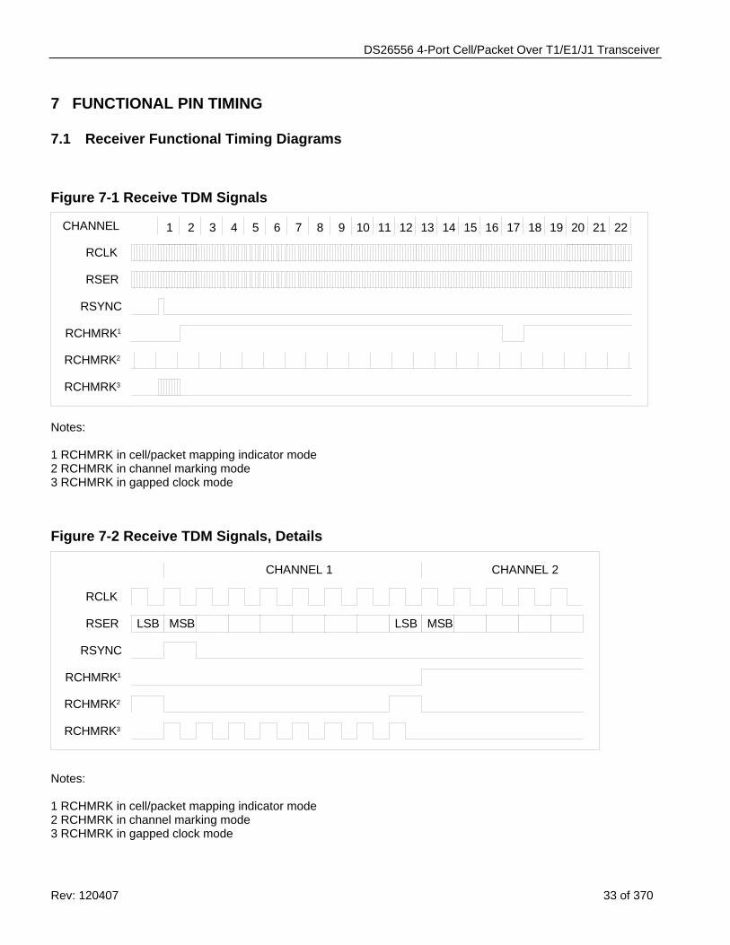
DS26556 4-Port Cell/Packet Over T1/E1/J1 Transceiver
Rev: 120407 33 of 370
7 FUNCTIONAL PIN TIMING
7.1 Receiver Functional Timing Diagrams
Figure 7-1 Receive TDM Signals
CHANNEL
RSYNC
RCHMRK2
RCHMRK1
RCHMRK3
1 2 3 4 5 6 7 8 9 10 11 12 13 14 15 16 17 18 19 20 21 22
RCLK
RSER
Notes: 1 RCHMRK in cell/packet mapping indicator mode 2 RCHMRK in channel marking mode 3 RCHMRK in gapped clock mode
Figure 7-2 Receive TDM Signals, Details
RSYNC
RCHMRK2
RCHMRK1
RCHMRK3
RCLK
RSER MSB LSB
CHANNEL 1 CHANNEL 2
MSBLSB
Notes: 1 RCHMRK in cell/packet mapping indicator mode 2 RCHMRK in channel marking mode 3 RCHMRK in gapped clock mode
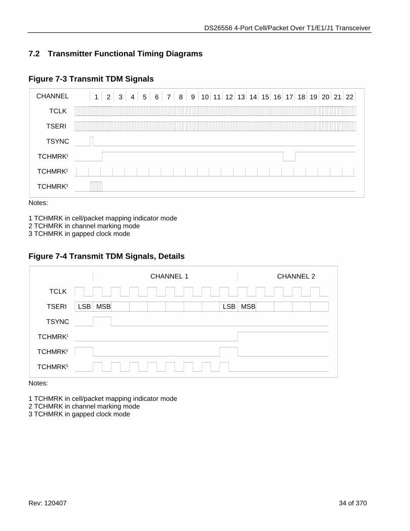
DS26556 4-Port Cell/Packet Over T1/E1/J1 Transceiver
Rev: 120407 34 of 370
7.2 Transmitter Functional Timing Diagrams
Figure 7-3 Transmit TDM Signals
CHANNEL
TSYNC
TCHMRK2
TCHMRK1
TCHMRK3
1 2 3 4 5 6 7 8 9 10 11 12 13 14 15 16 17 18 19 20 21 22
TCLK
TSERI
Notes: 1 TCHMRK in cell/packet mapping indicator mode 2 TCHMRK in channel marking mode 3 TCHMRK in gapped clock mode
Figure 7-4 Transmit TDM Signals, Details
TSYNC
TCHMRK2
TCHMRK1
TCHMRK3
TCLK
TSERI MSB LSB
CHANNEL 1 CHANNEL 2
MSBLSB
Notes: 1 TCHMRK in cell/packet mapping indicator mode 2 TCHMRK in channel marking mode 3 TCHMRK in gapped clock mode
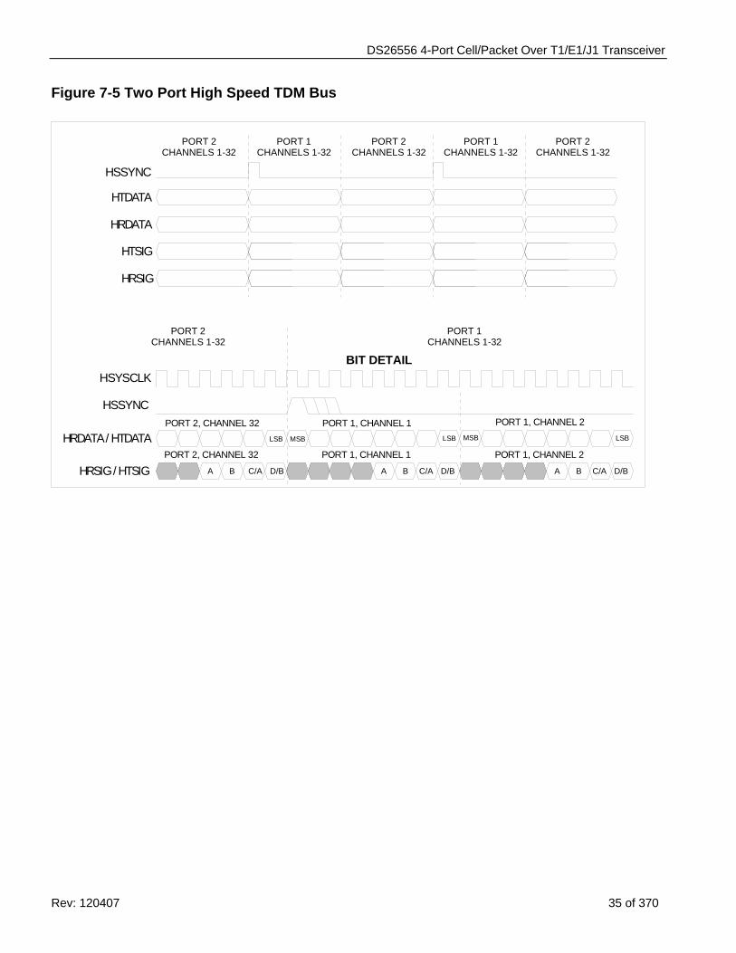
DS26556 4-Port Cell/Packet Over T1/E1/J1 Transceiver
Rev: 120407 35 of 370
Figure 7-5 Two Port High Speed TDM Bus
HRDATA / HTDATA LSB
HSYSCLK
HSSYNCPORT 2, CHANNEL 32
MSB LSB
PORT 1, CHANNEL 1
HRSIG / HTSIG PORT 2, CHANNEL 32 PORT 1, CHANNEL 1
MSB LSB
PORT 1, CHANNEL 2
PORT 1, CHANNEL 2
HTDATA
HSSYNC
BIT DETAIL
A B C/A D/B A B C/A D/B A B C/A D/B
HRDATA
HTSIG
PORT 2 CHANNELS 1-32
HRSIG
PORT 1 CHANNELS 1-32
PORT 2 CHANNELS 1-32
PORT 1 CHANNELS 1-32
PORT 2 CHANNELS 1-32
PORT 1 CHANNELS 1-32
PORT 2 CHANNELS 1-32
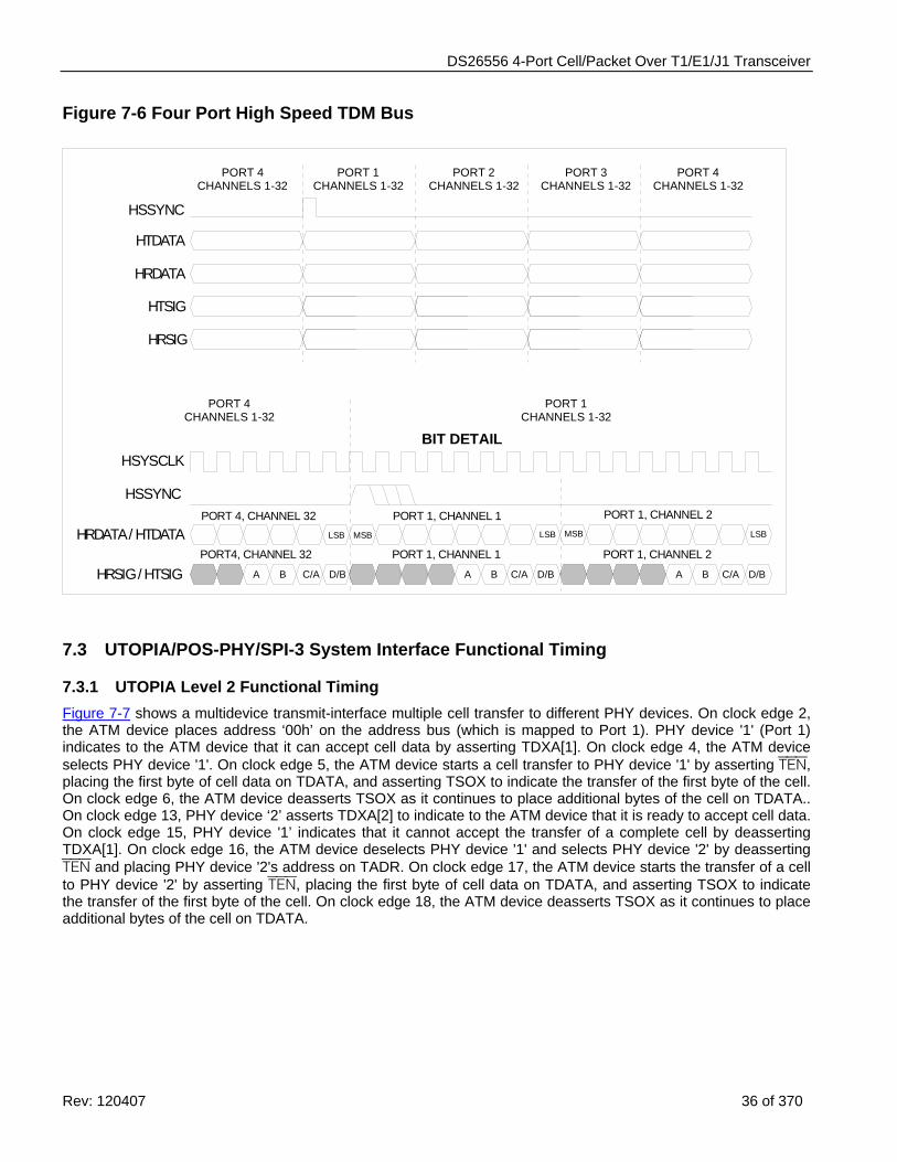
DS26556 4-Port Cell/Packet Over T1/E1/J1 Transceiver
Rev: 120407 36 of 370
Figure 7-6 Four Port High Speed TDM Bus
HRDATA / HTDATA LSB
HSYSCLK
HSSYNCPORT 4, CHANNEL 32
MSB LSB
PORT 1, CHANNEL 1
HRSIG / HTSIG PORT4, CHANNEL 32 PORT 1, CHANNEL 1
MSB LSB
PORT 1, CHANNEL 2
PORT 1, CHANNEL 2
HTDATA
HSSYNC
BIT DETAIL
A B C/A D/B A B C/A D/B A B C/A D/B
HRDATA
HTSIG
PORT 4 CHANNELS 1-32
HRSIG
PORT 1 CHANNELS 1-32
PORT 2 CHANNELS 1-32
PORT 3 CHANNELS 1-32
PORT 4 CHANNELS 1-32
PORT 1 CHANNELS 1-32
PORT 4 CHANNELS 1-32
7.3 UTOPIA/POS-PHY/SPI-3 System Interface Functional Timing
7.3.1 UTOPIA Level 2 Functional Timing Figure 7-7 shows a multidevice transmit-interface multiple cell transfer to different PHY devices. On clock edge 2, the ATM device places address ‘00h’ on the address bus (which is mapped to Port 1). PHY device '1' (Port 1) indicates to the ATM device that it can accept cell data by asserting TDXA[1]. On clock edge 4, the ATM device selects PHY device '1'. On clock edge 5, the ATM device starts a cell transfer to PHY device '1' by asserting TEN, placing the first byte of cell data on TDATA, and asserting TSOX to indicate the transfer of the first byte of the cell. On clock edge 6, the ATM device deasserts TSOX as it continues to place additional bytes of the cell on TDATA.. On clock edge 13, PHY device ‘2’ asserts TDXA[2] to indicate to the ATM device that it is ready to accept cell data. On clock edge 15, PHY device '1’ indicates that it cannot accept the transfer of a complete cell by deasserting TDXA[1]. On clock edge 16, the ATM device deselects PHY device '1' and selects PHY device '2' by deasserting TEN and placing PHY device '2's address on TADR. On clock edge 17, the ATM device starts the transfer of a cell to PHY device '2' by asserting TEN, placing the first byte of cell data on TDATA, and asserting TSOX to indicate the transfer of the first byte of the cell. On clock edge 18, the ATM device deasserts TSOX as it continues to place additional bytes of the cell on TDATA.
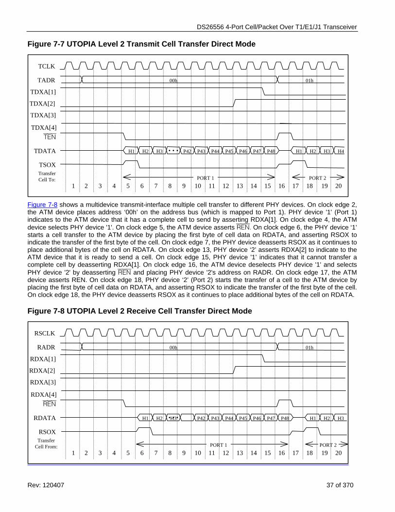
DS26556 4-Port Cell/Packet Over T1/E1/J1 Transceiver
Rev: 120407 37 of 370
Figure 7-7 UTOPIA Level 2 Transmit Cell Transfer Direct Mode
TADR
1
TEN
TDATA
TSOX
19 20
…
TCLK
H3 P43 P44 P45 P46 P47 P48P42H1 H2
01h00h
TransferCell To: PORT 1
H2 H3 H4
PORT 2
H1
2 3 4 5 76 8 10 11 12 13 14 15 16 17 189
TDXA[1]
TDXA[2]
TDXA[3]
TDXA[4]
Figure 7-8 shows a multidevice transmit-interface multiple cell transfer to different PHY devices. On clock edge 2, the ATM device places address ‘00h’ on the address bus (which is mapped to Port 1). PHY device '1' (Port 1) indicates to the ATM device that it has a complete cell to send by asserting RDXA[1]. On clock edge 4, the ATM device selects PHY device '1'. On clock edge 5, the ATM device asserts REN. On clock edge 6, the PHY device ‘1’ starts a cell transfer to the ATM device by placing the first byte of cell data on RDATA, and asserting RSOX to indicate the transfer of the first byte of the cell. On clock edge 7, the PHY device deasserts RSOX as it continues to place additional bytes of the cell on RDATA. On clock edge 13, PHY device ‘2’ asserts RDXA[2] to indicate to the ATM device that it is ready to send a cell. On clock edge 15, PHY device '1’ indicates that it cannot transfer a complete cell by deasserting RDXA[1]. On clock edge 16, the ATM device deselects PHY device '1' and selects PHY device '2' by deasserting REN and placing PHY device '2's address on RADR. On clock edge 17, the ATM device asserts REN. On clock edge 18, PHY device ‘2’ (Port 2) starts the transfer of a cell to the ATM device by placing the first byte of cell data on RDATA, and asserting RSOX to indicate the transfer of the first byte of the cell. On clock edge 18, the PHY device deasserts RSOX as it continues to place additional bytes of the cell on RDATA.
Figure 7-8 UTOPIA Level 2 Receive Cell Transfer Direct Mode
RADR
1
REN
RDATA
RSOX
19 20
…
RSCLK
H3 P43 P44 P45 P46 P47 P48P42H1 H2
01h00h
TransferCell From: PORT 1
H2 H3
PORT 2
H1
2 3 4 5 76 8 10 11 12 13 14 15 16 17 189
RDXA[1]
RDXA[2]
RDXA[3]
RDXA[4]
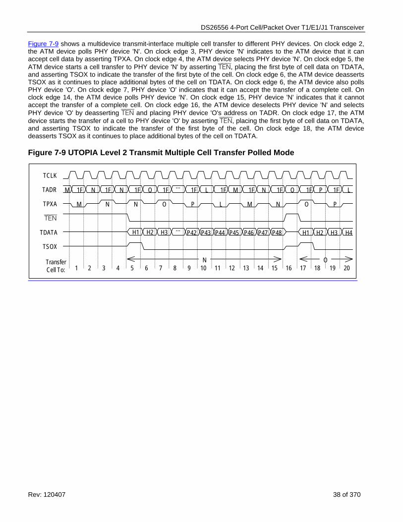
DS26556 4-Port Cell/Packet Over T1/E1/J1 Transceiver
Rev: 120407 38 of 370
Figure 7-9 shows a multidevice transmit-interface multiple cell transfer to different PHY devices. On clock edge 2, the ATM device polls PHY device 'N'. On clock edge 3, PHY device 'N' indicates to the ATM device that it can accept cell data by asserting TPXA. On clock edge 4, the ATM device selects PHY device 'N'. On clock edge 5, the ATM device starts a cell transfer to PHY device 'N' by asserting TEN, placing the first byte of cell data on TDATA, and asserting TSOX to indicate the transfer of the first byte of the cell. On clock edge 6, the ATM device deasserts TSOX as it continues to place additional bytes of the cell on TDATA. On clock edge 6, the ATM device also polls PHY device 'O'. On clock edge 7, PHY device 'O' indicates that it can accept the transfer of a complete cell. On clock edge 14, the ATM device polls PHY device 'N'. On clock edge 15, PHY device 'N' indicates that it cannot accept the transfer of a complete cell. On clock edge 16, the ATM device deselects PHY device 'N' and selects PHY device 'O' by deasserting TEN and placing PHY device 'O's address on TADR. On clock edge 17, the ATM device starts the transfer of a cell to PHY device 'O' by asserting TEN, placing the first byte of cell data on TDATA, and asserting TSOX to indicate the transfer of the first byte of the cell. On clock edge 18, the ATM device deasserts TSOX as it continues to place additional bytes of the cell on TDATA.
Figure 7-9 UTOPIA Level 2 Transmit Multiple Cell Transfer Polled Mode
TADR
1
TPXA
TEN
TDATA
TSOX
19 20
…
TCLK
H3 P43 P44 P45 P46 P47 P48P42H1 H2
1F 1F N 1F 1FO 1F L 1F M 1F N 1F O 1F P 1F LN
M N N O P L M N O P
M …
TransferCell To:
N
H2 H3 H4
O
H1
2 3 4 5 76 8 10 11 12 13 14 15 16 17 189
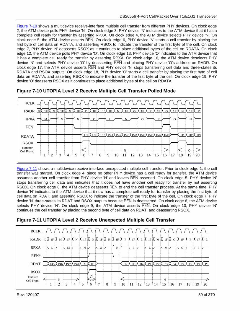
DS26556 4-Port Cell/Packet Over T1/E1/J1 Transceiver
Rev: 120407 39 of 370
Figure 7-10 shows a multidevice receive-interface multiple cell transfer from different PHY devices. On clock edge 2, the ATM device polls PHY device 'N'. On clock edge 3, PHY device 'N' indicates to the ATM device that it has a complete cell ready for transfer by asserting RPXA. On clock edge 4, the ATM device selects PHY device 'N'. On clock edge 5, the ATM device asserts REN. On clock edge 6, PHY device 'N' starts a cell transfer by placing the first byte of cell data on RDATA, and asserting RSOX to indicate the transfer of the first byte of the cell. On clock edge 7, PHY device 'N' deasserts RSOX as it continues to place additional bytes of the cell on RDATA. On clock edge 12, the ATM device polls PHY device 'O'. On clock edge 13, PHY device 'O' indicates to the ATM device that it has a complete cell ready for transfer by asserting RPXA. On clock edge 16, the ATM device deselects PHY device 'N' and selects PHY device 'O' by deasserting REN and placing PHY device 'O's address on RADR. On clock edge 17, the ATM device asserts REN and PHY device 'N' stops transferring cell data and three-states its RDATA and RSOX outputs. On clock edge 18, PHY device 'O' starts a cell transfer by placing the first byte of cell data on RDATA, and asserting RSOX to indicate the transfer of the first byte of the cell. On clock edge 19, PHY device 'O' deasserts RSOX as it continues to place additional bytes of the cell on RDATA.
Figure 7-10 UTOPIA Level 2 Receive Multiple Cell Transfer Polled Mode
RADR
1
RPXA
REN
RDATA
RSOX
19 20
…
RCLK
1F 1F N 1F 1FO 1F M 1F O 1F P 1F O 1F N 1F PN
M N N O L M O P O N
M …
H1 H2
TransferCell From: N
H3
O
H2H1P43 P44 P45 P46 P47 P48P42P41
2 3 4 5 76 8 10 11 12 13 14 15 16 17 189
Figure 7-11 shows a multidevice receive-interface unexpected multiple cell transfer. Prior to clock edge 1, the cell transfer was started. On clock edge 4, since no other PHY device has a cell ready for transfer, the ATM device assumes another cell transfer from PHY device 'N' and leaves REN asserted. On clock edge 5, PHY device 'N' stops transferring cell data and indicates that it does not have another cell ready for transfer by not asserting RSOX. On clock edge 6, the ATM device deasserts REN to end the cell transfer process. At the same time, PHY device 'N' indicates to the ATM device that it now has a complete cell ready for transfer by placing the first byte of cell data on RDAT, and asserting RSOX to indicate the transfer of the first byte of the cell. On clock edge 7, PHY device 'N' three-states its RDAT and RSOX outputs because REN is deasserted. On clock edge 8, the ATM device selects PHY device 'N'. On clock edge 9, the ATM device asserts REN. On clock edge 10, PHY device 'N' continues the cell transfer by placing the second byte of cell data on RDAT, and deasserting RSOX.
Figure 7-11 UTOPIA Level 2 Receive Unexpected Multiple Cell Transfer
RADR
1
RPXA
REN*
RDAT
RSOX
19 20
RCLK
1F 1F N 1F 1FO 1F P 1F L 1F M 1F O 1F P 1F LM
L M N O N P L M O P
L
TransferCell From: N
P45 P46 P47 P48 X H1
2 3 4 5 76 8 10 11 12 13 14 15 16 17 189
N
H2 P2P1H3 H4 P6P5P3 P4 P7 P8
NN
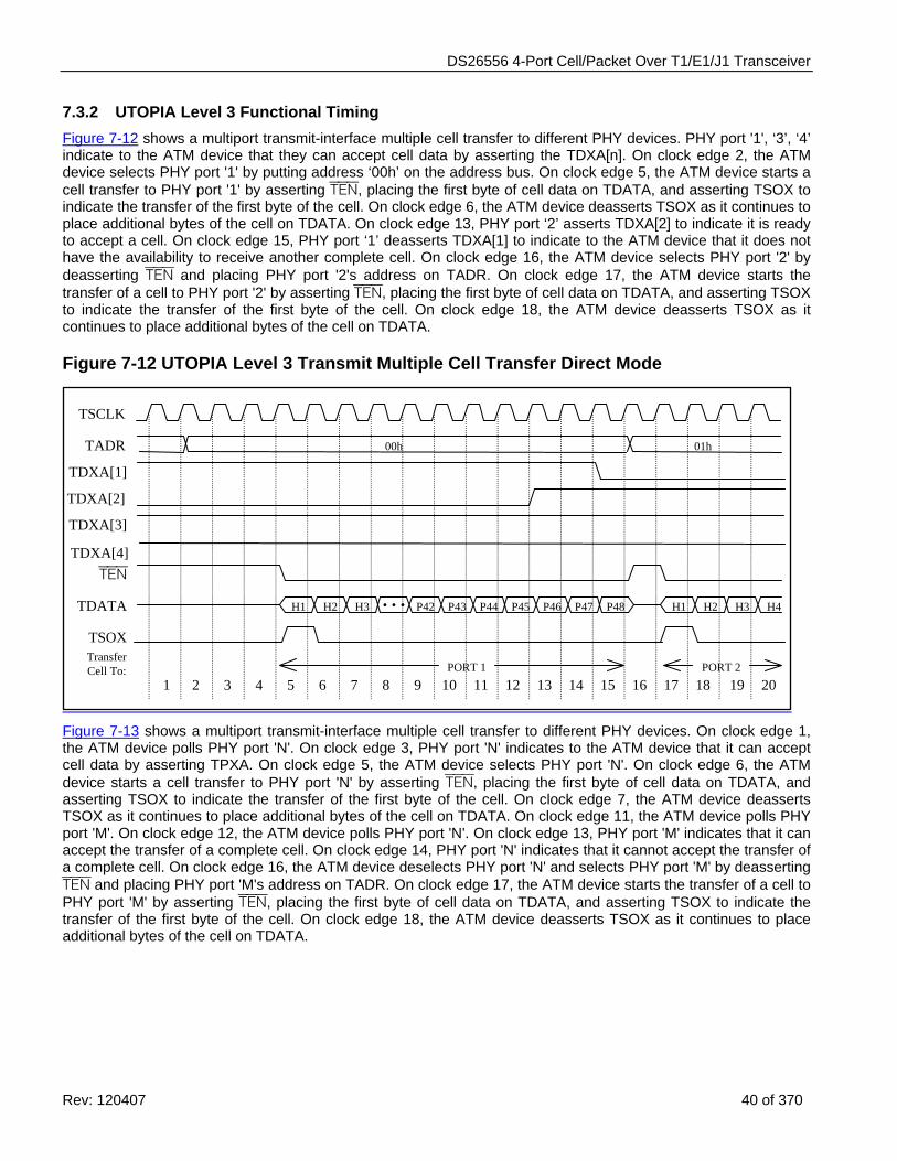
DS26556 4-Port Cell/Packet Over T1/E1/J1 Transceiver
Rev: 120407 40 of 370
7.3.2 UTOPIA Level 3 Functional Timing Figure 7-12 shows a multiport transmit-interface multiple cell transfer to different PHY devices. PHY port '1', ‘3’, ‘4’ indicate to the ATM device that they can accept cell data by asserting the TDXA[n]. On clock edge 2, the ATM device selects PHY port '1' by putting address ‘00h’ on the address bus. On clock edge 5, the ATM device starts a cell transfer to PHY port '1' by asserting TEN, placing the first byte of cell data on TDATA, and asserting TSOX to indicate the transfer of the first byte of the cell. On clock edge 6, the ATM device deasserts TSOX as it continues to place additional bytes of the cell on TDATA. On clock edge 13, PHY port ‘2’ asserts TDXA[2] to indicate it is ready to accept a cell. On clock edge 15, PHY port ‘1’ deasserts TDXA[1] to indicate to the ATM device that it does not have the availability to receive another complete cell. On clock edge 16, the ATM device selects PHY port '2' by deasserting TEN and placing PHY port '2's address on TADR. On clock edge 17, the ATM device starts the transfer of a cell to PHY port '2' by asserting TEN, placing the first byte of cell data on TDATA, and asserting TSOX to indicate the transfer of the first byte of the cell. On clock edge 18, the ATM device deasserts TSOX as it continues to place additional bytes of the cell on TDATA.
Figure 7-12 UTOPIA Level 3 Transmit Multiple Cell Transfer Direct Mode
TADR
1
TEN
TDATA
TSOX
19 20
…
TSCLK
H3 P43 P44 P45 P46 P47 P48P42H1 H2
01h00h
TransferCell To: PORT 1
H2 H3 H4
PORT 2
H1
2 3 4 5 76 8 10 11 12 13 14 15 16 17 189
TDXA[1]
TDXA[2]
TDXA[3]
TDXA[4]
Figure 7-13 shows a multiport transmit-interface multiple cell transfer to different PHY devices. On clock edge 1, the ATM device polls PHY port 'N'. On clock edge 3, PHY port 'N' indicates to the ATM device that it can accept cell data by asserting TPXA. On clock edge 5, the ATM device selects PHY port 'N'. On clock edge 6, the ATM device starts a cell transfer to PHY port 'N' by asserting TEN, placing the first byte of cell data on TDATA, and asserting TSOX to indicate the transfer of the first byte of the cell. On clock edge 7, the ATM device deasserts TSOX as it continues to place additional bytes of the cell on TDATA. On clock edge 11, the ATM device polls PHY port 'M'. On clock edge 12, the ATM device polls PHY port 'N'. On clock edge 13, PHY port 'M' indicates that it can accept the transfer of a complete cell. On clock edge 14, PHY port 'N' indicates that it cannot accept the transfer of a complete cell. On clock edge 16, the ATM device deselects PHY port 'N' and selects PHY port 'M' by deasserting TEN and placing PHY port 'M's address on TADR. On clock edge 17, the ATM device starts the transfer of a cell to PHY port 'M' by asserting TEN, placing the first byte of cell data on TDATA, and asserting TSOX to indicate the transfer of the first byte of the cell. On clock edge 18, the ATM device deasserts TSOX as it continues to place additional bytes of the cell on TDATA.
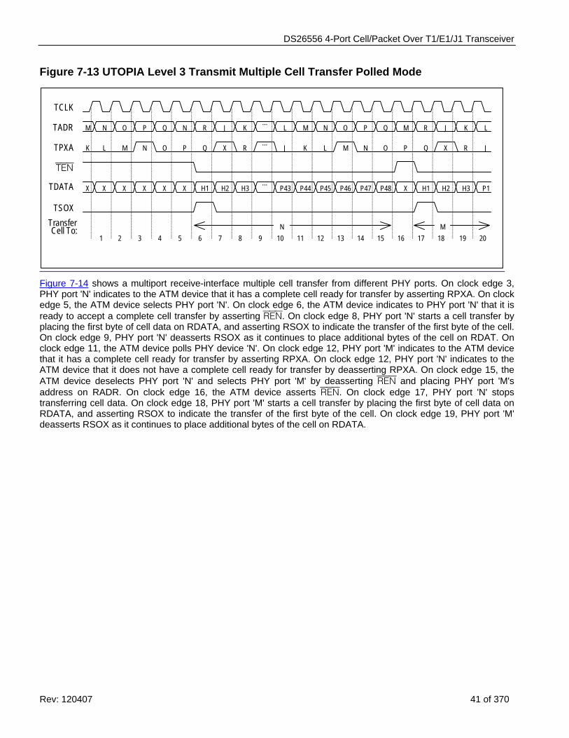
DS26556 4-Port Cell/Packet Over T1/E1/J1 Transceiver
Rev: 120407 41 of 370
Figure 7-13 UTOPIA Level 3 Transmit Multiple Cell Transfer Polled Mode
TADR
1
TPXA
TEN
TDATA
TSOX
19 20
TCLK
P44 P45 P46 P47 P48P43X
N P Q N L M N O P Q R J K LO
L N P K M O Q R
M
TransferCell To: N
2 3 4 5 76 8 10 11 12 13 14 15 16 17 189
M J L N P X J
X X XXX H3H2
R KJ
O Q R
…
…
X
H1
K
M
X H1 H2 H3 P1
…
M
Figure 7-14 shows a multiport receive-interface multiple cell transfer from different PHY ports. On clock edge 3, PHY port 'N' indicates to the ATM device that it has a complete cell ready for transfer by asserting RPXA. On clock edge 5, the ATM device selects PHY port 'N'. On clock edge 6, the ATM device indicates to PHY port 'N' that it is ready to accept a complete cell transfer by asserting REN. On clock edge 8, PHY port 'N' starts a cell transfer by placing the first byte of cell data on RDATA, and asserting RSOX to indicate the transfer of the first byte of the cell. On clock edge 9, PHY port 'N' deasserts RSOX as it continues to place additional bytes of the cell on RDAT. On clock edge 11, the ATM device polls PHY device 'N'. On clock edge 12, PHY port 'M' indicates to the ATM device that it has a complete cell ready for transfer by asserting RPXA. On clock edge 12, PHY port 'N' indicates to the ATM device that it does not have a complete cell ready for transfer by deasserting RPXA. On clock edge 15, the ATM device deselects PHY port 'N' and selects PHY port 'M' by deasserting REN and placing PHY port 'M's address on RADR. On clock edge 16, the ATM device asserts REN. On clock edge 17, PHY port 'N' stops transferring cell data. On clock edge 18, PHY port 'M' starts a cell transfer by placing the first byte of cell data on RDATA, and asserting RSOX to indicate the transfer of the first byte of the cell. On clock edge 19, PHY port 'M' deasserts RSOX as it continues to place additional bytes of the cell on RDATA.
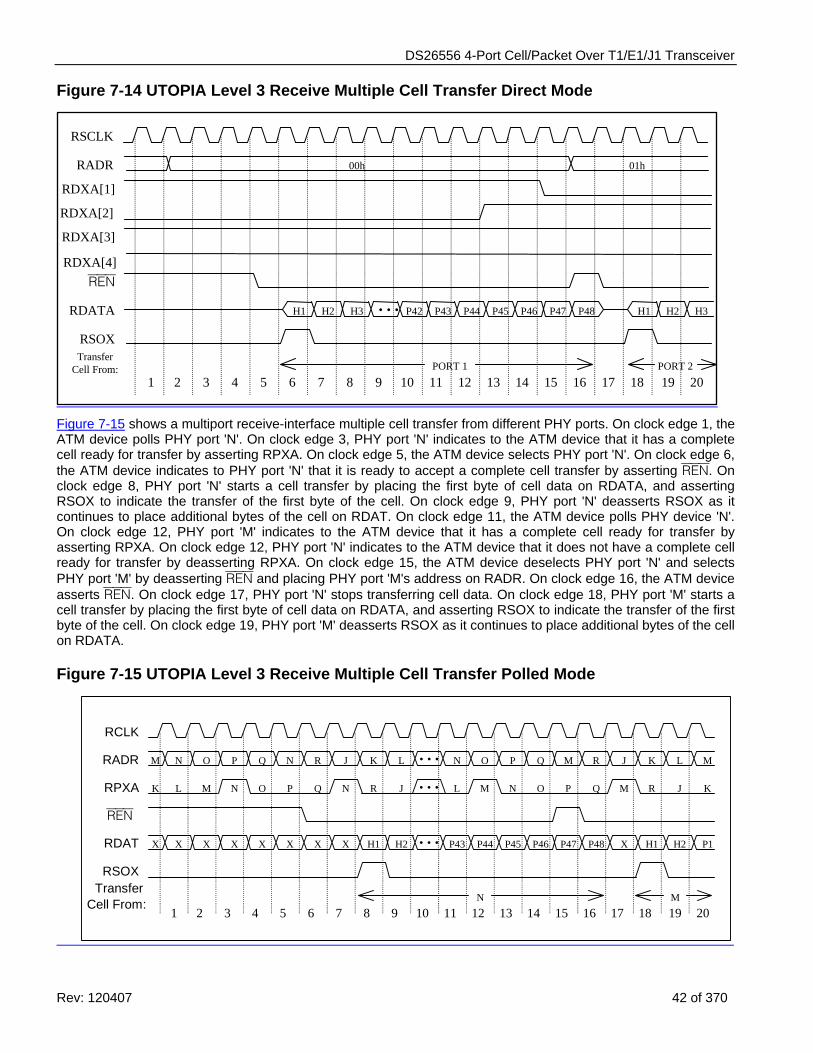
DS26556 4-Port Cell/Packet Over T1/E1/J1 Transceiver
Rev: 120407 42 of 370
Figure 7-14 UTOPIA Level 3 Receive Multiple Cell Transfer Direct Mode
RADR
1
REN
RDATA
RSOX
19 20
…
RSCLK
H3 P43 P44 P45 P46 P47 P48P42H1 H2
01h00h
TransferCell From: PORT 1
H2 H3
PORT 2
H1
2 3 4 5 76 8 10 11 12 13 14 15 16 17 189
RDXA[1]
RDXA[2]
RDXA[3]
RDXA[4]
Figure 7-15 shows a multiport receive-interface multiple cell transfer from different PHY ports. On clock edge 1, the ATM device polls PHY port 'N'. On clock edge 3, PHY port 'N' indicates to the ATM device that it has a complete cell ready for transfer by asserting RPXA. On clock edge 5, the ATM device selects PHY port 'N'. On clock edge 6, the ATM device indicates to PHY port 'N' that it is ready to accept a complete cell transfer by asserting REN. On clock edge 8, PHY port 'N' starts a cell transfer by placing the first byte of cell data on RDATA, and asserting RSOX to indicate the transfer of the first byte of the cell. On clock edge 9, PHY port 'N' deasserts RSOX as it continues to place additional bytes of the cell on RDAT. On clock edge 11, the ATM device polls PHY device 'N'. On clock edge 12, PHY port 'M' indicates to the ATM device that it has a complete cell ready for transfer by asserting RPXA. On clock edge 12, PHY port 'N' indicates to the ATM device that it does not have a complete cell ready for transfer by deasserting RPXA. On clock edge 15, the ATM device deselects PHY port 'N' and selects PHY port 'M' by deasserting REN and placing PHY port 'M's address on RADR. On clock edge 16, the ATM device asserts REN. On clock edge 17, PHY port 'N' stops transferring cell data. On clock edge 18, PHY port 'M' starts a cell transfer by placing the first byte of cell data on RDATA, and asserting RSOX to indicate the transfer of the first byte of the cell. On clock edge 19, PHY port 'M' deasserts RSOX as it continues to place additional bytes of the cell on RDATA.
Figure 7-15 UTOPIA Level 3 Receive Multiple Cell Transfer Polled Mode
RADR
1
RPXA
REN
RDAT
RSOX
19 20
RCLK
X
N P Q N L J MO
L N P M
M
TransferCell From:
2 3 4 5 76 8 10 11 12 13 14 15 16 17 189
M J K
X X XXX
R KJ
O Q R
…N
N
XH2 …H1
K
X X P1
…N O P Q R
M O QL N P
P44 P45 P46 P47 P48P43
M K L
JR
H1 H2
M
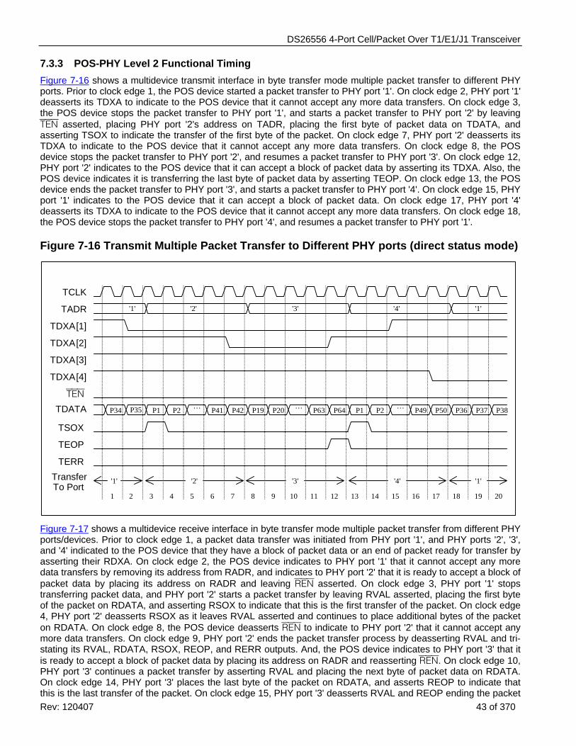
DS26556 4-Port Cell/Packet Over T1/E1/J1 Transceiver
Rev: 120407 43 of 370
7.3.3 POS-PHY Level 2 Functional Timing Figure 7-16 shows a multidevice transmit interface in byte transfer mode multiple packet transfer to different PHY ports. Prior to clock edge 1, the POS device started a packet transfer to PHY port '1'. On clock edge 2, PHY port '1' deasserts its TDXA to indicate to the POS device that it cannot accept any more data transfers. On clock edge 3, the POS device stops the packet transfer to PHY port '1', and starts a packet transfer to PHY port '2' by leaving TEN asserted, placing PHY port '2's address on TADR, placing the first byte of packet data on TDATA, and asserting TSOX to indicate the transfer of the first byte of the packet. On clock edge 7, PHY port '2' deasserts its TDXA to indicate to the POS device that it cannot accept any more data transfers. On clock edge 8, the POS device stops the packet transfer to PHY port '2', and resumes a packet transfer to PHY port '3'. On clock edge 12, PHY port '2' indicates to the POS device that it can accept a block of packet data by asserting its TDXA. Also, the POS device indicates it is transferring the last byte of packet data by asserting TEOP. On clock edge 13, the POS device ends the packet transfer to PHY port '3', and starts a packet transfer to PHY port '4'. On clock edge 15, PHY port '1' indicates to the POS device that it can accept a block of packet data. On clock edge 17, PHY port '4' deasserts its TDXA to indicate to the POS device that it cannot accept any more data transfers. On clock edge 18, the POS device stops the packet transfer to PHY port '4', and resumes a packet transfer to PHY port '1'.
Figure 7-16 Transmit Multiple Packet Transfer to Different PHY ports (direct status mode)
P36 P37 P38
'1'
TEN
TSOX
TEOP
TERR
TDATA
TCLK
TDXA[1]
TADR
TDXA[2]
TDXA[3]
TDXA[4]
1 19 202 3 4 5 76 8 10 11 12 13 14 15 16 17 189
TransferTo Port
P34 P19 P20 P49P63 P1 P2…
'3'
P64
'4'
… P50
'1'
P1 P2 P41… P42P35
'2'
'1' '2' '3' '4' '1'
Figure 7-17 shows a multidevice receive interface in byte transfer mode multiple packet transfer from different PHY ports/devices. Prior to clock edge 1, a packet data transfer was initiated from PHY port '1', and PHY ports '2', '3', and '4' indicated to the POS device that they have a block of packet data or an end of packet ready for transfer by asserting their RDXA. On clock edge 2, the POS device indicates to PHY port '1' that it cannot accept any more data transfers by removing its address from RADR, and indicates to PHY port '2' that it is ready to accept a block of packet data by placing its address on RADR and leaving REN asserted. On clock edge 3, PHY port '1' stops transferring packet data, and PHY port '2' starts a packet transfer by leaving RVAL asserted, placing the first byte of the packet on RDATA, and asserting RSOX to indicate that this is the first transfer of the packet. On clock edge 4, PHY port '2' deasserts RSOX as it leaves RVAL asserted and continues to place additional bytes of the packet on RDATA. On clock edge 8, the POS device deasserts REN to indicate to PHY port '2' that it cannot accept any more data transfers. On clock edge 9, PHY port '2' ends the packet transfer process by deasserting RVAL and tri-stating its RVAL, RDATA, RSOX, REOP, and RERR outputs. And, the POS device indicates to PHY port '3' that it is ready to accept a block of packet data by placing its address on RADR and reasserting REN. On clock edge 10, PHY port '3' continues a packet transfer by asserting RVAL and placing the next byte of packet data on RDATA. On clock edge 14, PHY port '3' places the last byte of the packet on RDATA, and asserts REOP to indicate that this is the last transfer of the packet. On clock edge 15, PHY port '3' deasserts RVAL and REOP ending the packet
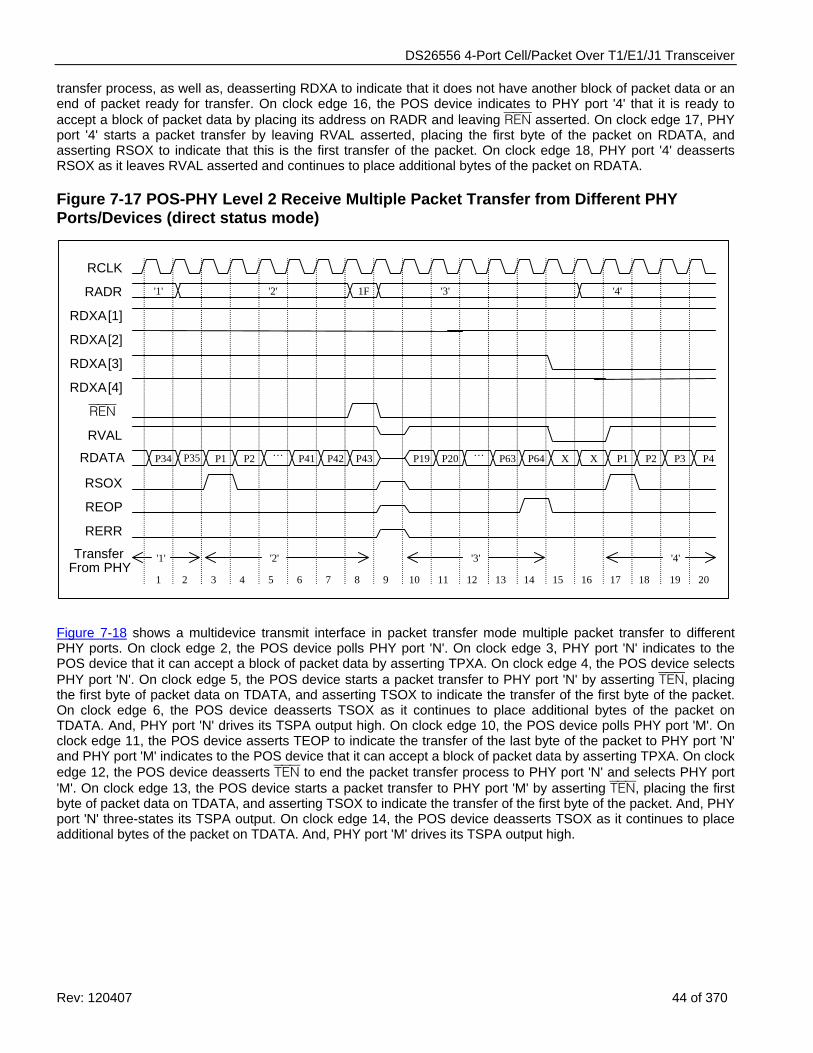
DS26556 4-Port Cell/Packet Over T1/E1/J1 Transceiver
Rev: 120407 44 of 370
transfer process, as well as, deasserting RDXA to indicate that it does not have another block of packet data or an end of packet ready for transfer. On clock edge 16, the POS device indicates to PHY port '4' that it is ready to accept a block of packet data by placing its address on RADR and leaving REN asserted. On clock edge 17, PHY port '4' starts a packet transfer by leaving RVAL asserted, placing the first byte of the packet on RDATA, and asserting RSOX to indicate that this is the first transfer of the packet. On clock edge 18, PHY port '4' deasserts RSOX as it leaves RVAL asserted and continues to place additional bytes of the packet on RDATA.
Figure 7-17 POS-PHY Level 2 Receive Multiple Packet Transfer from Different PHY Ports/Devices (direct status mode)
RCLK
RDXA[1]
RADR
RDXA[2]
RDXA[3]
RDXA[4]
1 19 202 3 4 5 76 8 10 11 12 13 14 15 16 17 189
RSOX
REOP
RERR
RDATA
TransferFrom PHY
RVAL
REN
P34 P1 P2 P41… P42P35
'4'1F '3''1' '2'
…P19 P20 P2P63 X XP64 P3
'1' '2' '3' '4'
P4P43 P1
Figure 7-18 shows a multidevice transmit interface in packet transfer mode multiple packet transfer to different PHY ports. On clock edge 2, the POS device polls PHY port 'N'. On clock edge 3, PHY port 'N' indicates to the POS device that it can accept a block of packet data by asserting TPXA. On clock edge 4, the POS device selects PHY port 'N'. On clock edge 5, the POS device starts a packet transfer to PHY port 'N' by asserting TEN, placing the first byte of packet data on TDATA, and asserting TSOX to indicate the transfer of the first byte of the packet. On clock edge 6, the POS device deasserts TSOX as it continues to place additional bytes of the packet on TDATA. And, PHY port 'N' drives its TSPA output high. On clock edge 10, the POS device polls PHY port 'M'. On clock edge 11, the POS device asserts TEOP to indicate the transfer of the last byte of the packet to PHY port 'N' and PHY port 'M' indicates to the POS device that it can accept a block of packet data by asserting TPXA. On clock edge 12, the POS device deasserts TEN to end the packet transfer process to PHY port 'N' and selects PHY port 'M'. On clock edge 13, the POS device starts a packet transfer to PHY port 'M' by asserting TEN, placing the first byte of packet data on TDATA, and asserting TSOX to indicate the transfer of the first byte of the packet. And, PHY port 'N' three-states its TSPA output. On clock edge 14, the POS device deasserts TSOX as it continues to place additional bytes of the packet on TDATA. And, PHY port 'M' drives its TSPA output high.
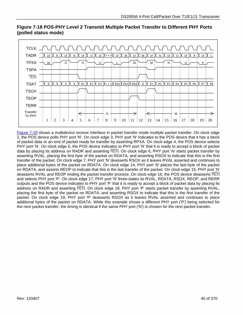
DS26556 4-Port Cell/Packet Over T1/E1/J1 Transceiver
Rev: 120407 45 of 370
Figure 7-18 POS-PHY Level 2 Transmit Multiple Packet Transfer to Different PHY Ports (polled status mode)
TCLK
TADR
TPXA
1F 1F N 1F 1FO 1F M 1F M 1F N 1F O 1F P 1F LN …M N N O L M
1 19 202 3 4 5 76 8 10 11 12 13 14 15 16 17 189
X P5XX P6 P7 P8X
TEN
TSOX
TEOP
TERR
TDAT
TransferTo PHY
P1 P2 P3 … P62 P63 P64 X P1 P2 P3 P4
N
M N O P
TSPA
M
Figure 7-19 shows a multidevice receive interface in packet transfer mode multiple packet transfer. On clock edge 2, the POS device polls PHY port 'N'. On clock edge 3, PHY port 'N' indicates to the POS device that it has a block of packet data or an end of packet ready for transfer by asserting RPXA. On clock edge 4, the POS device selects PHY port 'N'. On clock edge 5, the POS device indicates to PHY port 'N' that it is ready to accept a block of packet data by placing its address on RADR and asserting REN. On clock edge 6, PHY port 'N' starts packet transfer by asserting RVAL, placing the first byte of the packet on RDATA, and asserting RSOX to indicate that this is the first transfer of the packet. On clock edge 7, PHY port 'N' deasserts RSOX as it leaves RVAL asserted and continues to place additional bytes of the packet on RDATA. On clock edge 14, PHY port 'N' places the last byte of the packet on RDATA, and asserts REOP to indicate that this is the last transfer of the packet. On clock edge 15, PHY port 'N' deasserts RVAL and REOP ending the packet transfer process. On clock edge 16, the POS device deasserts REN and selects PHY port 'P'. On clock edge 17, PHY port 'N' three-states its RVAL, RDATA, RSOX, REOP, and RERR outputs and the POS device indicates to PHY port 'P' that it is ready to accept a block of packet data by placing its address on RADR and asserting REN. On clock edge 18, PHY port 'P' starts packet transfer by asserting RVAL, placing the first byte of the packet on RDATA, and asserting RSOX to indicate that this is the first transfer of the packet. On clock edge 19, PHY port 'P' deasserts RSOX as it leaves RVAL asserted and continues to place additional bytes of the packet on RDATA. While this example shows a different PHY port ('P') being selected for the next packet transfer, the timing is identical if the same PHY port ('N') is chosen for the next packet transfer.
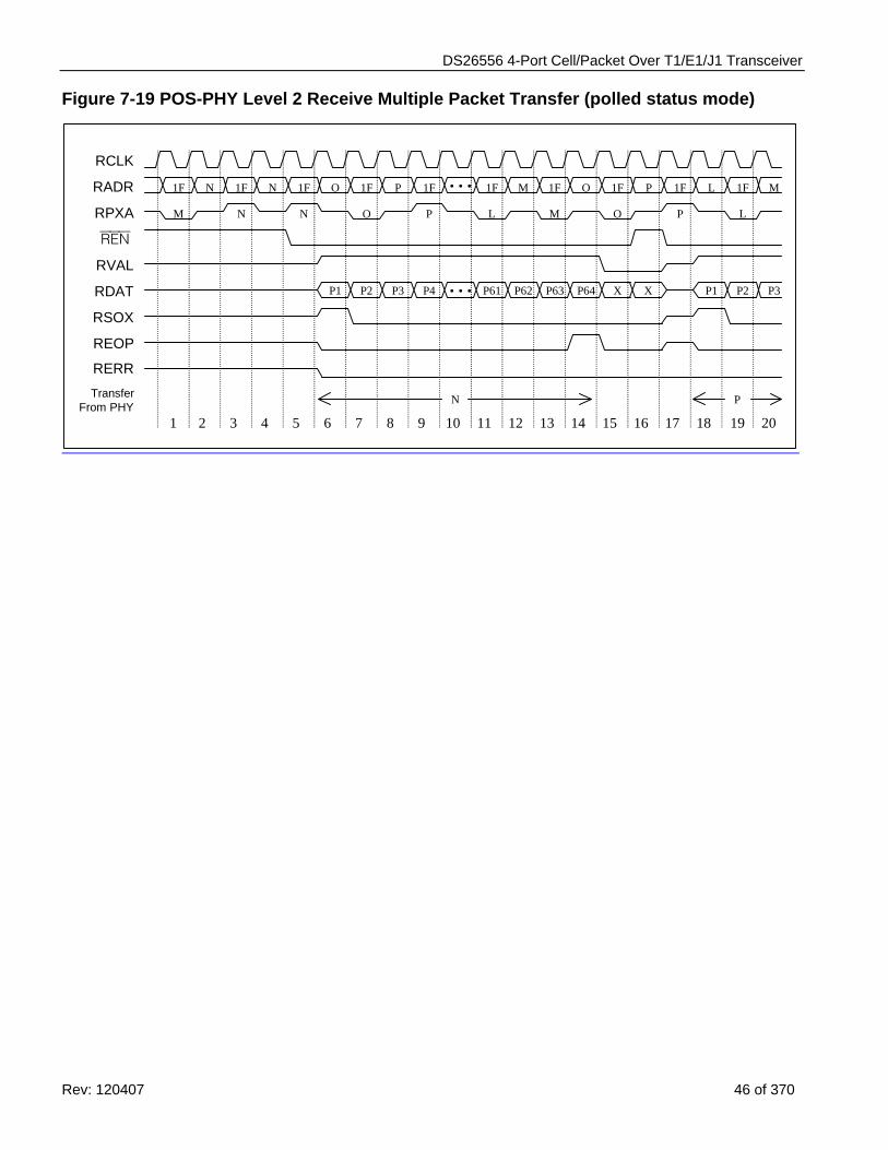
DS26556 4-Port Cell/Packet Over T1/E1/J1 Transceiver
Rev: 120407 46 of 370
Figure 7-19 POS-PHY Level 2 Receive Multiple Packet Transfer (polled status mode)
RCLK
RPXA
RADR
1 19 202 3 4 5 76 8 10 11 12 13 14 15 16 17 189
…P4 P61 P62 P63
RSOX
REOP
RERR
RDAT
TransferFrom PHY
N
RVAL
REN
P2P1
1F 1F N 1F 1FO 1F 1F M 1F O 1F P 1F L 1F MN …M N N O P L M O P L
P
P3 P3P64 X X
P
P2P1
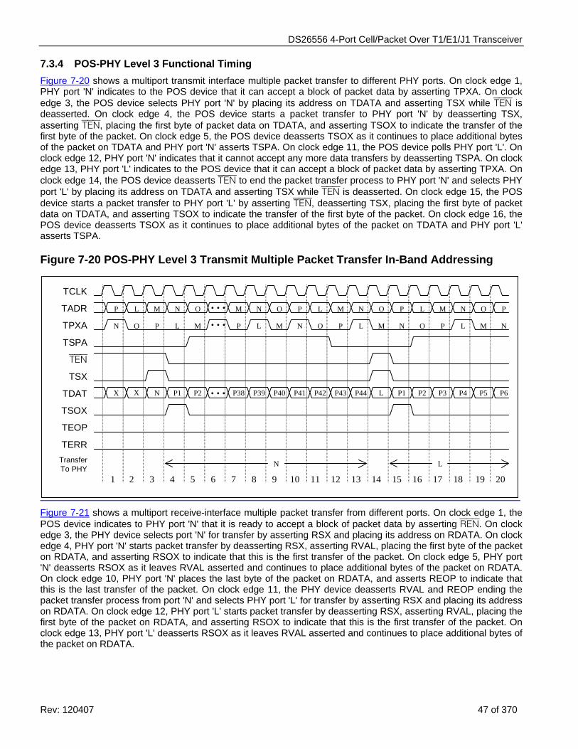
DS26556 4-Port Cell/Packet Over T1/E1/J1 Transceiver
Rev: 120407 47 of 370
7.3.4 POS-PHY Level 3 Functional Timing Figure 7-20 shows a multiport transmit interface multiple packet transfer to different PHY ports. On clock edge 1, PHY port 'N' indicates to the POS device that it can accept a block of packet data by asserting TPXA. On clock edge 3, the POS device selects PHY port 'N' by placing its address on TDATA and asserting TSX while TEN is deasserted. On clock edge 4, the POS device starts a packet transfer to PHY port 'N' by deasserting TSX, asserting TEN, placing the first byte of packet data on TDATA, and asserting TSOX to indicate the transfer of the first byte of the packet. On clock edge 5, the POS device deasserts TSOX as it continues to place additional bytes of the packet on TDATA and PHY port 'N' asserts TSPA. On clock edge 11, the POS device polls PHY port 'L'. On clock edge 12, PHY port 'N' indicates that it cannot accept any more data transfers by deasserting TSPA. On clock edge 13, PHY port 'L' indicates to the POS device that it can accept a block of packet data by asserting TPXA. On clock edge 14, the POS device deasserts TEN to end the packet transfer process to PHY port 'N' and selects PHY port 'L' by placing its address on TDATA and asserting TSX while TEN is deasserted. On clock edge 15, the POS device starts a packet transfer to PHY port 'L' by asserting TEN, deasserting TSX, placing the first byte of packet data on TDATA, and asserting TSOX to indicate the transfer of the first byte of the packet. On clock edge 16, the POS device deasserts TSOX as it continues to place additional bytes of the packet on TDATA and PHY port 'L' asserts TSPA.
Figure 7-20 POS-PHY Level 3 Transmit Multiple Packet Transfer In-Band Addressing
M N O LP
P39P38
P M OL N
P40 P41 P42
TCLK
TADR
TPXA
P M N O P L M N O PL
N
1 19 202 3 4 5 76 8 10 11 12 13 14 15 16 17 189
X P5 P6X
TEN
TEOP
TERR
TDAT
TransferTo PHY
N
L N P M
TSPA
O P M O L N
P43
TSOX
P44 L P1 P2 P3 P4
TSX
M O …ML
N
…
N P1 P2 …
P
L
Figure 7-21 shows a multiport receive-interface multiple packet transfer from different ports. On clock edge 1, the POS device indicates to PHY port 'N' that it is ready to accept a block of packet data by asserting REN. On clock edge 3, the PHY device selects port 'N' for transfer by asserting RSX and placing its address on RDATA. On clock edge 4, PHY port 'N' starts packet transfer by deasserting RSX, asserting RVAL, placing the first byte of the packet on RDATA, and asserting RSOX to indicate that this is the first transfer of the packet. On clock edge 5, PHY port 'N' deasserts RSOX as it leaves RVAL asserted and continues to place additional bytes of the packet on RDATA. On clock edge 10, PHY port 'N' places the last byte of the packet on RDATA, and asserts REOP to indicate that this is the last transfer of the packet. On clock edge 11, the PHY device deasserts RVAL and REOP ending the packet transfer process from port 'N' and selects PHY port 'L' for transfer by asserting RSX and placing its address on RDATA. On clock edge 12, PHY port 'L' starts packet transfer by deasserting RSX, asserting RVAL, placing the first byte of the packet on RDATA, and asserting RSOX to indicate that this is the first transfer of the packet. On clock edge 13, PHY port 'L' deasserts RSOX as it leaves RVAL asserted and continues to place additional bytes of the packet on RDATA.
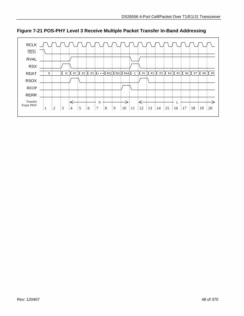
DS26556 4-Port Cell/Packet Over T1/E1/J1 Transceiver
Rev: 120407 48 of 370
Figure 7-21 POS-PHY Level 3 Receive Multiple Packet Transfer In-Band Addressing
TransferFrom PHY
N L
RCLK
1 19 202 3 4 5 76 8 10 11 12 13 14 15 16 17 189
RDAT
RSOX
REOP
RERR
X N P1 P2 … P62 P63 P64 L P9
REN
RVAL
P3
RSX
P1 P2 P3 P4 P5 P6 P7 P8
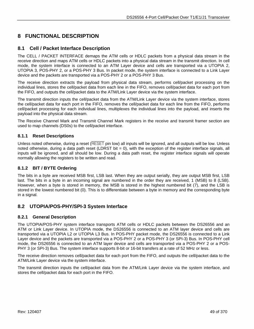
DS26556 4-Port Cell/Packet Over T1/E1/J1 Transceiver
Rev: 120407 49 of 370
8 FUNCTIONAL DESCRIPTION
8.1 Cell / Packet Interface Description The CELL / PACKET INTERFACE demaps the ATM cells or HDLC packets from a physical data stream in the receive direction and maps ATM cells or HDLC packets into a physical data stream in the transmit direction. In cell mode, the system interface is connected to an ATM Layer device and cells are transported via a UTOPIA 2, UTOPIA 3, POS-PHY 2, or a POS-PHY 3 Bus. In packet mode, the system interface is connected to a Link Layer device and the packets are transported via a POS-PHY 2 or a POS-PHY 3 Bus.
The receive direction extracts the payload from physical data stream, performs cell/packet processing on the individual lines, stores the cell/packet data from each line in the FIFO, removes cell/packet data for each port from the FIFO, and outputs the cell/packet data to the ATM/Link Layer device via the system interface.
The transmit direction inputs the cell/packet data from the ATM/Link Layer device via the system interface, stores the cell/packet data for each port in the FIFO, removes the cell/packet data for each line from the FIFO, performs cell/packet processing for each individual lines, multiplexes the individual lines into the payload, and inserts the payload into the physical data stream.
The Receive Channel Mark and Transmit Channel Mark registers in the receive and transmit framer section are used to map channels (DS0s) to the cell/packet interface.
8.1.1 Reset Descriptions Unless noted otherwise, during a reset (RESET pin low) all inputs will be ignored, and all outputs will be low. Unless noted otherwise, during a data path reset (LDRST bit = 0), with the exception of the register interface signals, all inputs will be ignored, and all should be low. During a data path reset, the register interface signals will operate normally allowing the registers to be written and read.
8.1.2 BIT / BYTE Ordering The bits in a byte are received MSB first, LSB last. When they are output serially, they are output MSB first, LSB last. The bits in a byte in an incoming signal are numbered in the order they are received, 1 (MSB) to 8 (LSB). However, when a byte is stored in memory, the MSB is stored in the highest numbered bit (7), and the LSB is stored in the lowest numbered bit (0). This is to differentiate between a byte in memory and the corresponding byte in a signal.
8.2 UTOPIA/POS-PHY/SPI-3 System Interface
8.2.1 General Description The UTOPIA/POS-PHY system interface transports ATM cells or HDLC packets between the DS26556 and an ATM or Link Layer device. In UTOPIA mode, the DS26556 is connected to an ATM layer device and cells are transported via a UTOPIA L2 or UTOPIA L3 Bus. In POS-PHY packet mode, the DS26556 is connected to a Link Layer device and the packets are transported via a POS-PHY 2 or a POS-PHY 3 (or SPI-3) Bus. In POS-PHY cell mode, the DS26556 is connected to an ATM layer device and cells are transported via a POS-PHY 2 or a POS-PHY 3 (or SPI-3) Bus. The system interface supports 8-bit or 16-bit transfers at a rate of 52 MHz or less.
The receive direction removes cell/packet data for each port from the FIFO, and outputs the cell/packet data to the ATM/Link Layer device via the system interface.
The transmit direction inputs the cell/packet data from the ATM/Link Layer device via the system interface, and stores the cell/packet data for each port in the FIFO.
DS26556 4-Port Cell/Packet Over T1/E1/J1 Transceiver
Rev: 120407 50 of 370
8.2.2 Features • Programmable system interface type – When performing cell mapping/demapping, the system interface can
be programmed as a UTOPIA Level 2 Bus, a UTOPIA Level 3 Bus, a POS-PHY Level 2 Bus, or a POS-PHY Level 3 (or SPI-3) Bus. When performing packet mapping/demapping, the system interface can be programmed as a POS-PHY Level 2 Bus or a POS-PHY Level 3 (or SPI-3) Bus.
• Selectable system interface bus width – The data bus can be a 16-bit or 8-bit bus at operations speeds up to 52 MHz.
• Supports multiple ports on the system interface – Each T1 or E1 line has its own port address for access via the system interface.
• Supports per-port system loopback – Each port can be placed in system loopback which causes cells/packets from the transmit FIFO to be looped back to the receive FIFO.
• System interface byte reordering – In 16-bit modes, the received/transmitted order of the bytes transferred across the system interface is programmable. i.e., the first byte received/transmitted by ATM cell / packet processing can be transferred in [15:8] or [7:0].
8.2.6 System Interface Bus Controller The Transmit and Receive System Interface Bus Controller can be programmed to operate as a UTOPIA Level 2, UTOPIA Level 3, POS-PHY Level 2, or POS-PHY Level 3 (or SPI-3) bus controller. It controls the system interface bus timing and provides a common interface to the Transmit and Receive FIFO for FIFO status polling and cell/packet data transfer. Normally, the first byte transmitted is transferred across the system interface as the most significant byte (TDATA[15:8] in 16-bit mode). If byte reordering is enabled, the first byte transmitted is transferred across the system interface as the least significant byte (TDATA[7:0]).On the receive side, the first byte received is transferred across the system interface as the most significant byte (RDATA[15:8] in 16-bit mode). If byte reordering is enabled, the first byte received is transferred across the system interface as the least significant byte (RDATA[7:0]).
See Figure 8-1 and Figure 8-2. Byte reordering is ignored in 8-bit mode.
Figure 8-1 Normal Packet Format in 16-Bit Mode
Bit 15 Bit 0
Byte 1 Byte 2 1st Transfer
Byte 3 Byte 4 2nd Transfer • • •
• • •
Byte 2n-3 Byte 2n-2 (n-1)th Transfer
Byte 2n-1 Byte 2n nth Transfer
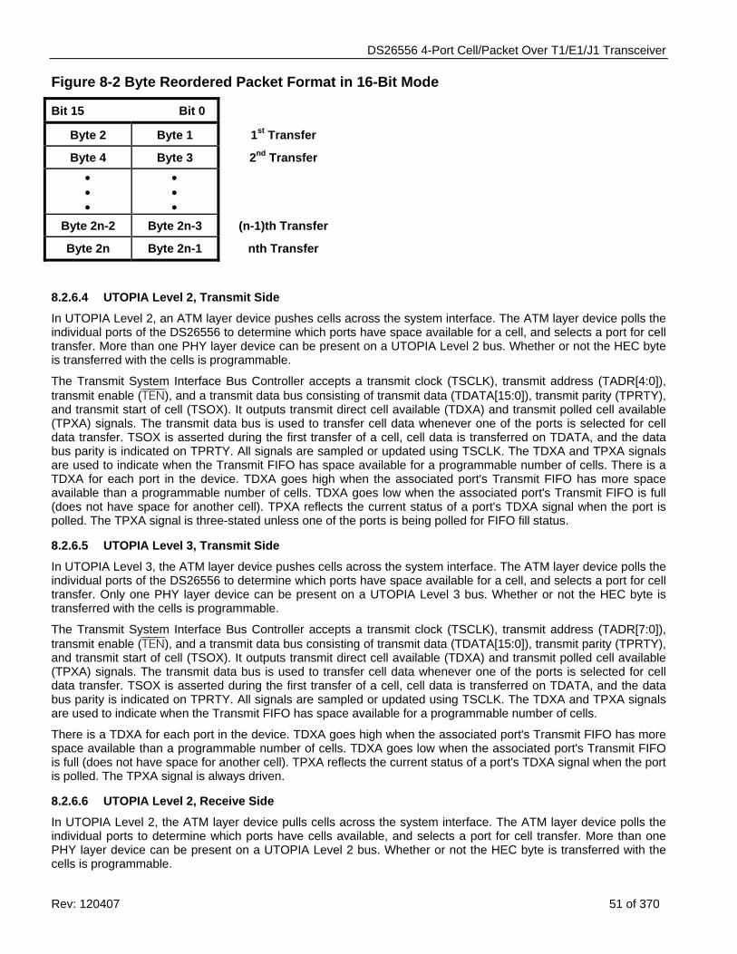
DS26556 4-Port Cell/Packet Over T1/E1/J1 Transceiver
Rev: 120407 51 of 370
Figure 8-2 Byte Reordered Packet Format in 16-Bit Mode
Bit 15 Bit 0
Byte 2 Byte 1 1st Transfer
Byte 4 Byte 3 2nd Transfer • • •
• • •
Byte 2n-2 Byte 2n-3 (n-1)th Transfer
Byte 2n Byte 2n-1 nth Transfer
8.2.6.4 UTOPIA Level 2, Transmit Side
In UTOPIA Level 2, an ATM layer device pushes cells across the system interface. The ATM layer device polls the individual ports of the DS26556 to determine which ports have space available for a cell, and selects a port for cell transfer. More than one PHY layer device can be present on a UTOPIA Level 2 bus. Whether or not the HEC byte is transferred with the cells is programmable.
The Transmit System Interface Bus Controller accepts a transmit clock (TSCLK), transmit address (TADR[4:0]), transmit enable (TEN), and a transmit data bus consisting of transmit data (TDATA[15:0]), transmit parity (TPRTY), and transmit start of cell (TSOX). It outputs transmit direct cell available (TDXA) and transmit polled cell available (TPXA) signals. The transmit data bus is used to transfer cell data whenever one of the ports is selected for cell data transfer. TSOX is asserted during the first transfer of a cell, cell data is transferred on TDATA, and the data bus parity is indicated on TPRTY. All signals are sampled or updated using TSCLK. The TDXA and TPXA signals are used to indicate when the Transmit FIFO has space available for a programmable number of cells. There is a TDXA for each port in the device. TDXA goes high when the associated port's Transmit FIFO has more space available than a programmable number of cells. TDXA goes low when the associated port's Transmit FIFO is full (does not have space for another cell). TPXA reflects the current status of a port's TDXA signal when the port is polled. The TPXA signal is three-stated unless one of the ports is being polled for FIFO fill status.
8.2.6.5 UTOPIA Level 3, Transmit Side
In UTOPIA Level 3, the ATM layer device pushes cells across the system interface. The ATM layer device polls the individual ports of the DS26556 to determine which ports have space available for a cell, and selects a port for cell transfer. Only one PHY layer device can be present on a UTOPIA Level 3 bus. Whether or not the HEC byte is transferred with the cells is programmable.
The Transmit System Interface Bus Controller accepts a transmit clock (TSCLK), transmit address (TADR[7:0]), transmit enable (TEN), and a transmit data bus consisting of transmit data (TDATA[15:0]), transmit parity (TPRTY), and transmit start of cell (TSOX). It outputs transmit direct cell available (TDXA) and transmit polled cell available (TPXA) signals. The transmit data bus is used to transfer cell data whenever one of the ports is selected for cell data transfer. TSOX is asserted during the first transfer of a cell, cell data is transferred on TDATA, and the data bus parity is indicated on TPRTY. All signals are sampled or updated using TSCLK. The TDXA and TPXA signals are used to indicate when the Transmit FIFO has space available for a programmable number of cells.
There is a TDXA for each port in the device. TDXA goes high when the associated port's Transmit FIFO has more space available than a programmable number of cells. TDXA goes low when the associated port's Transmit FIFO is full (does not have space for another cell). TPXA reflects the current status of a port's TDXA signal when the port is polled. The TPXA signal is always driven.
8.2.6.6 UTOPIA Level 2, Receive Side
In UTOPIA Level 2, the ATM layer device pulls cells across the system interface. The ATM layer device polls the individual ports to determine which ports have cells available, and selects a port for cell transfer. More than one PHY layer device can be present on a UTOPIA Level 2 bus. Whether or not the HEC byte is transferred with the cells is programmable.
DS26556 4-Port Cell/Packet Over T1/E1/J1 Transceiver
Rev: 120407 52 of 370
The Receive System Interface Bus Controller accepts a receive clock (RSCLK), receive address (RADR[4:0]), and receive enable (REN). It outputs a receive data bus consisting of receive data (RDATA[15:0]), receive parity (RPRTY), and receive start of cell (RSOX), as well as, receive direct cell available (RDXA) and receive polled cell available (RPXA) signals. The receive bus is used to transfer cell data whenever one of the ports is selected for cell data transfer. RSOX is asserted during the first transfer of a cell, cell data is transferred on RDATA, and the data bus parity is indicated on RPRTY. All signals are sampled or updated using RSCLK. The data bus is three-stated unless REN is asserted (low) and one of the ports is selected for data transfer. The RDXA and RPXA signals are used to indicate when the Receive FIFO has a programmable number of cells available for transfer. There is an RDXA for each port in the device. RDXA goes high when the associated port's Receive FIFO contains more than a programmable number of cells. RDXA goes low when the associated port's Receive FIFO is empty (does not contain any cells). RPXA reflects the current status of a port's RDXA signal when the port is polled. The RPXA signal is three-stated unless one of the ports is being polled for FIFO fill status.
8.2.6.2 UTOPIA Level 3, Receive Side
In UTOPIA Level 3, the ATM layer device pulls cells across the system interface. The ATM layer device polls the individual ports to determine which ports have cells available, and selects a port for cell transfer. Only one PHY layer device can be present on a UTOPIA Level 3 bus. Whether or not the HEC byte is transferred with the cells is programmable.
The Receive System Interface Bus Controller accepts a receive clock (RSCLK), receive address (RADR[7:0]), and receive enable (REN). It outputs a receive data bus consisting of receive data (RDATA[15:0]), receive parity (RPRTY), and receive start of cell (RSOX), as well as, receive direct cell available (RDXA) and receive polled cell available (RPXA) signals. The receive data bus is used to transfer cell data whenever one of the ports is selected for cell data transfer. RSOX is asserted during the first transfer of a cell, cell data is transferred on RDATA, and the data bus parity is indicated on RPRTY. All signals are sampled or updated using RSCLK. The data bus is always driven. The RDXA and RPXA signals are used to indicate when the Receive FIFO has a programmable number of cells available for transfer. There is an RDXA for each port in the device. RDXA goes high when the associated port's Receive FIFO contains more than a programmable number of cells. RDXA goes low when the associated port's Receive FIFO is empty (does not contain any cell ends). RPXA reflects the current status of a port's RDXA signal when the port is polled. The RPXA signal is always driven.
8.2.6.3 POS-PHY Level 2, Transmit Side
In POS-PHY Level 2, the Link layer device pushes packets across the system interface. The Link layer device polls the individual ports of the DS26556 to determine which ports have space available for packet data, and selects a port for packet data transfer. More than one PHY layer device can be present on a POS-PHY Level 2 bus.
The Transmit System Interface Bus Controller accepts a transmit clock (TSCLK), transmit address (TADR[4:0]), transmit enable (TEN), and a transmit data bus consisting of transmit data (TDATA[15:0]), transmit parity (TPRTY), transmit start of packet (TSOX), transmit end of packet (TEOP), transmit error (TERR), and transmit modulus (TMOD). It outputs transmit direct packet available (TDXA), transmit polled packet available (TPXA), and transmit selected packet available (TSPA) signals. The transmit data bus is used to transfer packet data whenever one of the ports is selected for packet data transfer. TSOX is asserted during the first transfer of a packet, TEOP is asserted during the last transfer of a packet, TERR is asserted when a packet has an error, TMOD indicates the number of bytes transferred on TDATA during the last transfer of a packet, packet data is transferred on TDATA, and the data bus parity is indicated on TPRTY. All signals are sampled and updated using TSCLK. The TDXA, TPXA, and TSPA signals are used to indicate when the Transmit FIFO has space available for a programmable number of bytes. There is a TDXA for each port in the device. TDXA goes high when the associated port's Transmit FIFO has space available for more than a programmable number of bytes. TDXA goes low when the associated port's Transmit FIFO is full. TPXA reflects the current status of a port's TDXA signal when the system interface is in polled mode. TSPA reflects the current status of a port's TDXA signal when the port is selected. The TSPA signal is three-stated unless TEN is asserted (low) and one of the ports is selected for packet data transfer. The TPXA signal is three-stated unless one of the ports is being polled for FIFO fill status.
DS26556 4-Port Cell/Packet Over T1/E1/J1 Transceiver
Rev: 120407 53 of 370
8.2.6.4 POS-PHY Level 3 (or SPI-3), Transmit Side
In POS-PHY Level 3 (or SPI-3), the Link layer device pushes packets across the system interface. The Link layer device polls the individual ports of the DS26556 to determine which ports have space available for packet data, and selects a port for packet data transfer. Only one PHY layer device can be present on a POS-PHY Level 3 (or SPI-3) bus.
The Transmit System Interface Bus Controller accepts a transmit clock (TSCLK), transmit enable (TEN), and a transmit data bus consisting of transmit data (TDATA[15:0]), transmit parity (TPRTY), transmit start of packet (TSOX), transmit end of packet (TEOP), transmit error (TERR), transmit start of transfer (TSX), and transmit modulus (TMOD). It outputs transmit direct packet available (TDXA), transmit polled packet available (TPXA), and transmit selected packet available (TSPA) signals. The transmit bus is used to transfer packet data whenever one of the ports is selected for packet data transfer. TSOX is asserted during the first transfer of a packet, TEOP is asserted during the last transfer of a packet, TERR is asserted when a packet has an error, TMOD indicates the number of bytes transferred on TDATA during the last transfer of a packet, TSX is asserted when the selected FIFO's port address has been placed on TDATA, packet data is transferred on TDATA, and the data bus parity is indicated on TPRTY. All signals are sampled and updated using TSCLK. The TDXA, TPXA, and TSPA signals are used to indicate when the Transmit FIFO has space available for a programmable number of bytes. There is a TDXA for each port in the device. TDXA goes high when the associated port's Transmit FIFO has space available for more than a programmable number of bytes. TDXA goes low when the associated port's Transmit FIFO is full. TPXA reflects the current status of a port's TDXA signal when the port is polled. TSPA reflects the current status of a port's TDXA signal when the port is selected. The TPXA and TSPA signals are always driven.
8.2.6.5 POS-PHY Level 2, Receive Side
In POS-PHY Level 2, the Link layer device pulls packets across the system interface. The Link layer device polls the individual ports to determine which ports have packet data available, and selects a port for packet data transfer. More than one PHY layer device can be present on a POS-PHY Level 2 bus.
The Receive System Interface Bus Controller accepts a receive clock (RSCLK), receive address (RADR[4:0]), and receive enable (REN). It outputs a receive data bus consisting of receive data (RDATA[15:0]), receive parity (RPRTY), receive start of packet (RSOX), receive end of packet (REOP), receive error (RERR), receive data valid (RVAL), and receive modulus (RMOD), as well as, a receive direct packet available (RDXA) signal and a receive polled packet available (RPXA) signal. The receive data bus is used to transfer packet data whenever one of the ports is selected for packet data transfer. RSOX is asserted during the first transfer of a packet, REOP is asserted during the last transfer of a packet, RERR is asserted when a packet has an error, RMOD indicates the number of bytes transferred on RDATA during the last transfer of a packet, RVAL is asserted when the receive data bus is valid, RDATA transfers packet data, and RPRTY indicates the data bus parity. All signals are sampled and updated using RSCLK. The RDXA and RPXA signals are used to indicate when the Receive FIFO has a programmable number of bytes or an end of packet available for transfer. There is an RDXA for each port in the device. RDXA goes high when the associated port's Receive FIFO contains more than a programmable number of bytes or an end of packet. RDXA goes low when the associated port's Receive FIFO is empty. RPXA reflects the current status of a port's RDXA signal when the port is polled. The data bus is three-stated unless REN is asserted (low) and one of the ports is selected for packet data transfer. The RPXA signal is three-stated unless one of the ports is being polled for FIFO fill status.
8.2.6.6 POS-PHY Level 3 (or SPI-3), Receive Side
In POS-PHY Level 3, the DS26556 pushes packets across the system interface. The DS26556 selects a port for packet data transfer when it has packet data available. Only one PHY layer device can be present on a POS-PHY Level 3 (or SPI-3) bus.
The Receive System Interface Bus Controller accepts a receive clock (RSCLK) and receive enable (REN). It outputs a receive data bus consisting of receive data (RDATA[15:0]), receive parity (RPRTY), receive start of packet (RSOX), receive end of packet (REOP), receive error (RERR), receive data valid (RVAL), receive start of transfer (RSX), and receive modulus (RMOD). The receive data bus is used to transfer packet data whenever one of the ports has packet data available for transfer. RSOX is asserted during the first transfer of a packet, REOP is asserted during the last transfer of a packet, RERR is asserted when a packet has an error, RMOD indicates the number of bytes transferred on RDATA during the last transfer of a packet, RSX is asserted when the Link layer port address has been placed on RDATA, RVAL is asserted when the receive data bus is valid, RDATA transfers
DS26556 4-Port Cell/Packet Over T1/E1/J1 Transceiver
Rev: 120407 54 of 370
packet data, and RPRTY indicates the data bus parity. All signals are sampled and updated using RSCLK. The data bus is always driven.
In POS-PHY Level 3 (or SPI-3) the Receive System Interface Bus Controller determines which port to transfer data from using a round-robin arbitration scheme (the ports are checked one after another in numerical order according to their line number x. A transfer is initiated from a port when it is not almost empty (contains more data than the almost empty level or contains an end of packet). Transfer from a port is terminated when the maximum burst length has been transferred, the FIFO is emptied, or an end of packet is transferred while the Receive FIFO is almost empty (contains the same or less data than the almost empty level and does not contain an end of packet). When a transfer is terminated, a transfer is initiated from the next available port that is not almost empty. At the end of a packet or between a transfer from one port and the transfer from the next port, RVAL will go low for a programmable number of clock cycles (0-7) to allow the POS-PHY master to halt data transfer. At the end of a packet, data transfer will continue from the same port if the port is not almost empty. When the maximum burst length has been transferred, data transfer will continue from the same port if no other port has data available, and the port is not almost empty. The maximum burst length is programmable (8 – 256 bytes in four byte increments), or can be disabled.
8.3 ATM Cell / HDLC Packet Processing
8.3.1 General Description The ATM cell / packet processing demaps the ATM cells or HDLC packets from the receive data stream and maps ATM cells or HDLC packets into the transmit data stream. ATM cell / packet processing supports any framed or unframed bit synchronous or byte synchronous (octet aligned) data stream.
The receive direction extracts the payload from physical data stream, performs cell/packet processing on the individual lines, and stores the cell/packet data from each line in the FIFO.
The transmit direction removes the cell/packet data for each line from the FIFO, performs cell/packet processing for each individual line and inserts the payload into the physical data stream.
8.3.2 Features
8.3.2.1 General • Supports bit or byte wide, framed or unframed data lines – Each port is programmable as bit synchronous
or octet aligned, the data stream can be framed or unframed, and the clock can be continuous or gapped. • Bit reordering – The received/transmitted order of the bits as transferred across the system interface is
programmable on a per-port basis. That is, in bit synchronous mode, the first bit received/transmitted by ATM cell/packet processing can be transferred in bit position 7 (15 or 7) or bit position 0 (8 or 0). In octet aligned mode, the bit received/transmitted by ATM cell/packet processing in bit position 7 can be transferred in bit position 7 (15 or 7) or bit position 0 (8 or 0).
8.3.2.2 ATM Cell Processor • Programmable HEC insertion and extraction – The transmit side can be programmed to accept cells from
the system interface that do or do not contain a HEC byte. If cells are transferred without a HEC byte, the HEC byte will be computed and inserted. If cells are transferred with a HEC byte, then the transferred HEC byte can be programmed to be passed through or overwritten with a newly calculated HEC. The receive side can be programmed to send cells to the system interface that do or don't contain the HEC byte.
• Programmable erred cell insertion – An HEC error mask can be programmed for insertion of single or multiple errors individually or continuously at a programmable rate.
• Programmable transmit cell synchronization – The transmit data line can be provisioned to be bit synchronous or octet aligned.
• Programmable header cell pass-through – Receive cell filtering can pass-through only those cells that matching a programmable header value.
• Selectable idle/unassigned/invalid/programmable header cell padding and filtering – Transmit cell padding can be programmed for idle cell or programmable header cell padding. The padded cell payload byte contents are also programmable. Receive cell filtering can be programmed for any combination of idle cell, unassigned cell, invalid cell, or programmable header cell filtering. Or, all cell filtering can be disabled.
• Optional header error correction – Receive side single bit header error correction can enabled.
DS26556 4-Port Cell/Packet Over T1/E1/J1 Transceiver
Rev: 120407 55 of 370
• Separate corrected and uncorrected erred cell counts – Separate counts of erred cells containing a corrected HEC error, and cells containing non-corrected HEC errors are kept.
• Optional HEC uncorrected erred cell filtering – Uncorrected erred cell extraction can be disabled. • Selectable cell scrambling/descrambling – Cell scrambling and/or descrambling can be disabled. The
scrambling can be a self-synchronous scrambler (x43 + 1) over the payload only, a self-synchronous scrambler over the entire cell, or a Distributed Sample Scrambler (x31 + x28 + 1).
• Optional HEC calculation coset polynomial addition – The performance of coset polynomial addition during HEC calculation can be disabled.
8.3.2.3 HDLC Packet Processor • Programmable FCS insertion and extraction – The transmit side can be programmed to accept packets
from the system interface that do or don't contain FCS bytes. If packets are transferred without FCS bytes, the FCS will be computed and appended to the packet. If packets are transferred with FCS bytes, then the FCS can be programmed to be passed through or overwritten with a newly calculated FCS. The receive side can be programmed to send packets to the system interface that do or don't contain FCS bytes.
• Programmable transmit packet synchronization – The transmit data line can be provisioned to be bit synchronous or octet aligned.
• Programmable FCS type – The FCS can be programmed to be a 16-bit FCS or a 32-bit FCS. • Supports FCS error insertion – FCS error insertion can be programmed for insertion of errors individually or
continuously at a programmable rate. • Supports bit or byte stuffing/destuffing – The bit or byte synchronous (octet aligned) mode determines the
bit or byte stuffing/destuffing. • Programmable packet size limits – The receive side can be programmed to abort packets over a
programmable maximum size or under a programmable minimum size. The maximum packet size allowed is 65,535 bytes.
• Selectable packet scrambling/descrambling – Packet scrambling and/or descrambling can be disabled. • Separate FCS erred packet and aborted packet counts – Separate counts of aborted packets, size violation
packets, and FCS erred packets are kept. • Optional erred packet filtering – Erred packet extraction can be disabled • Programmable inter-frame fill – The transmit inter-frame fill value is programmable.
8.3.3 Transmit Cell/Packet Processor The Transmit Cell Processor and Transmit Packet Processor both receive the 32-bit parallel data stream from the Transmit FIFO, however, only one of the processors will be enabled. Which processor is enabled is determined by the system interface mode. In UTOPIA mode, the Transmit Cell Processor is enabled. In POS-PHY mode, if the CPC1.PMCPE bit is low, the Transmit Packet Processor is enabled. If the CPC1.PMCPE bit (is high, the Transmit Cell Processor is enabled.
8.3.4 Receive Cell/Packet Processor The Receive Cell Processor and Receive Packet Processor both receive the incoming data stream from the Receive Framer (minus all overhead and stuff data), however, only one of the processors will be enabled. The other will be disabled. Which processor is enabled is determined by the system interface mode. In UTOPIA mode, the Receive Cell Processor is enabled. In POS-PHY mode, if the CPC1.PMCPE bit is low, the Receive Packet Processor is enabled. If the CPC1.PMCPE bit is high, the Receive Cell Processor is enabled.
The bits in a byte are received MSB first, LSB last. When they are output serially, they are output MSB first, LSB last. The bits in a byte in an incoming signal are numbered in the order they are received , 1 (MSB) to 8 (LSB). However, when a byte is stored in a register, the MSB is stored in the highest numbered bit (7], and the LSB is stored in the lowest numbered bit (0). This is to differentiate between a byte in a register and the corresponding byte in a signal.
DS26556 4-Port Cell/Packet Over T1/E1/J1 Transceiver
Rev: 120407 56 of 370
8.3.5 Cell Processor
8.3.5.1 Transmit Cell Processor
The Transmit Cell Processor accepts data from the Transmit FIFO and performs bit reordering, cell padding, HEC processing, cell error insertion, and cell scrambling. The data output from the Transmit Cell Processor can be either a serial data stream (bit synchronous mode) or an 8-bit parallel data stream (octet-aligned mode). Cell processing can be disabled. Disabling cell processing disables cell padding, HEC processing, and cell error insertion. Only bit reordering and cell scrambling are not disabled.
When cell processing is disabled, data is continually read out of the Transmit FIFO. When the Transmit FIFO is empty, the output data stream is padded with FFh until the Transmit FIFO contains more data than the "almost empty" level.
The 32-bit data words read from the Transmit FIFO are multiplexed into an 8-bit parallel data stream and passed on to bit reordering.
Bit reordering changes the bit order of each byte. If bit reordering is enabled, the incoming 8-bit data stream DT[7:0] with DT[7] being the MSB and DT[0] being the LSB is rearranged so that the MSB is in DT[0] and the LSB is in DT[7] of the outgoing data stream DT[7:0]. In bit synchronous mode, DT[7] is the first bit transmitted. If cell processing is disabled the data stream is passed on to cell scrambling, bypassing cell padding, HEC processing, and cell error insertion.
Cell padding inserts fill cells. After a cell end, fill cells are inserted into the data stream if the Transmit FIFO does not contain a complete cell. The fill cell type and fill cell payload value are programmable. The resulting data stream is passed on to HEC processing. If cell processing is disabled, cell padding will not be performed.
HEC processing calculates a HEC and inserts it into the cell. HEC calculation is a CRC-8 calculation over the four header bytes. The polynomial used is x8 + x2 + x + 1. The coset polynomial, x6 + x4 + x2 + 1, is added (modulo 2) to the residue. The calculated HEC is then inserted into the byte immediately following the header. HEC coset polynomial addition is programmable. If the cell received from the Transmit FIFO contains a HEC byte, the received HEC byte can be passed through or overwritten with the calculated HEC byte. HEC byte pass through is programmable. If the cell received from the Transmit FIFO does not contain a HEC byte, the calculated HEC byte is inserted into the cell. If cell processing is disabled, HEC processing will not be performed.
Cell error insertion inserts errors into the HEC byte. The HEC bits to be errored are programmable. Error insertion can be controlled by a register or by the manual error insertion input (TMEI). The error insertion initiation type (register or input) is programmable. If a register controls error insertion, the number and frequency of the errors are programmable. If cell processing is disabled, cell error insertion will not be performed.
Cell scrambling can scramble the 48-byte cell payload, scramble the entire cell data stream, or scramble the data stream with a Distributed Sample Scrambler (DSS). If the payload or the entire data stream is scrambled, a self-synchronous scrambler with a generation polynomial of x43 + 1 is used. For payload scrambling, the scrambler scrambles the 48-byte payload, and does not scramble the four header or the HEC bytes. For a DSS scrambled data stream, a distributed sample scrambler with a generation polynomial of x31 + x28 + 1 is used for scrambling. The transmit DSS scrambler scrambles the 48-byte payload and the four byte header. It scrambles the first HEC bit (HEC[1]) with the first transmit DSS scrambler sample (the transmit DSS scrambler bit from 211 bits earlier), scrambles the second HEC bit (HEC[2]) with the second transmit DSS scrambler sample (the current transmit DSS scrambler bit), and does not scramble the remaining HEC bits (HEC[3:8]). DSS scrambling can only be performed in bit synchronous mode. Cell scrambling is programmable (payload, entire data stream, or DSS). If cell processing is disabled, the entire data stream will be scrambled whenever scrambling is enabled
Once all cell processing has been completed, in bit synchronous mode, the 8-bit parallel data stream is multiplexed into a serial data stream and passed on. In octet aligned mode, the 8-bit parallel data stream is passed on.
DS26556 4-Port Cell/Packet Over T1/E1/J1 Transceiver
Rev: 120407 57 of 370
8.3.5.2 Receive Cell Processor
The Receive Cell Processor performs cell descrambling, cell delineation, cell filtering, header pattern comparison, OCD detection, HEC error monitoring, HEC byte filtering, and bit reordering. The data coming in can be either a serial data stream (bit synchronous mode) or an 8-bit parallel data stream (octet aligned mode). The type of data stream received affects cell descrambling and cell delineation, however, it does not affect OCD detection, HEC error monitoring, cell filtering, header pattern comparison, HEC byte filtering, or bit reordering. Cell processing can be disabled (clear-channel enable). Disabling cell processing disables cell delineation, OCD detection, cell filtering, header pattern comparison, HEC error monitoring, and HEC byte filtering. Only cell descrambling and bit reordering are not disabled.
Cell descrambling can descramble the 48-byte cell payload, descramble the entire cell data stream, or descramble a data stream scrambled by a Distributed Sample Scrambler (DSS). If the payload or the entire data stream is descrambled, a self-synchronous scrambler with a generation polynomial of x43 + 1 is used for descrambling. Payload descrambling descrambles the 48-byte payload, and does not descramble the four header bytes or the HEC byte. For a DSS scrambled data stream, a distributed sample scrambler with a generation polynomial of x31 + x28 + 1 is used for descrambling. The receive DSS scrambler is synchronized to the transmit DSS scrambler by DSS scrambler synchronization. DSS descrambling can only be performed in bit synchronous mode. Cell descrambling is programmable (payload, entire data stream, or DSS). In bit synchronous mode, descrambling is performed one bit at a time, and the serial data stream is demultiplexed in to an 8-bit data stream before being passed on. In octet aligned mode, descrambling is performed 8-bits at a time, and only payload or entire data stream descrambling can be performed. When cell processing is disabled, the entire data stream will be descrambled if descrambling is enabled.
DSS Scrambler Synchronization synchronizes the receive DSS scrambler with the transmit DSS scrambler used to scramble the incoming data stream. The DSS Scrambler Synchronization state machine has three states: "Acquisition", "Verification", and "Steady State". The "Acquisition" state adds the transmit DSS scrambler samples from 16 incoming cells into the receive DSS scrambler (32 samples total). The samples are derived from the two MSBs (HEC[1:2]) of the incoming HEC byte. Each time the samples in a cell are loaded into the receive DSS scrambler, the confidence counter is incremented. When the confidence counter reaches 16, DSS scrambler synchronization transitions to the “Verification” state. The "Verification" state verifies the samples in the incoming cells by comparing the samples from the cell with the corresponding receive DSS scrambler bits. Each time both samples from a cell match the corresponding receive DSS scrambler bits, the confidence counter is incremented. Each time one of the samples from a cell does not match the corresponding receive DSS scrambler bit, the confidence counter is decremented if the confidence counter reaches 24, DSS scrambler synchronization transitions to the “Steady State” state. If the confidence counter reaches 8, DSS scrambler synchronization transitions to the “Acquisition” state. The "Steady State" state continues to verify the samples in the incoming cells. Each time both samples from a cell match the corresponding receive DSS scrambler bits, the confidence counter is incremented (maximum count = 24). Each time one of the samples from a cell does not match the corresponding receive DSS scrambler bit, the confidence counter is decremented. If the confidence counter reaches 16, DSS scrambler synchronization transitions to the “Acquisition” state. The DSS scrambler synchronization state diagram is shown in Figure 8-3. DSS scrambler synchronization starts in the “Acquisition” state. Note: All ATM cells are discarded during the “Acquisition” and “Verification” states.
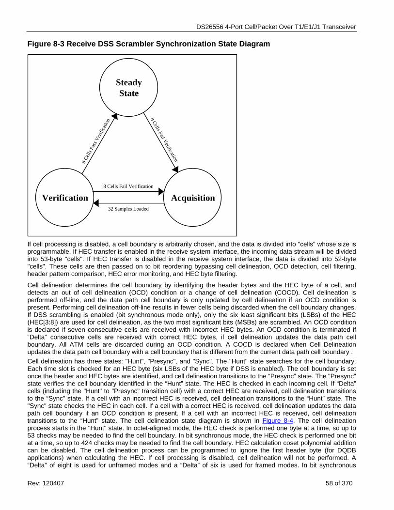
DS26556 4-Port Cell/Packet Over T1/E1/J1 Transceiver
Rev: 120407 58 of 370
Figure 8-3 Receive DSS Scrambler Synchronization State Diagram
SteadyState
AcquisitionVerification8 Cells Fail Verification
32 Samples Loaded
8 Cell
s Pas
s Ver
ifica
tion 8 Cells Fail Verification
If cell processing is disabled, a cell boundary is arbitrarily chosen, and the data is divided into "cells" whose size is programmable. If HEC transfer is enabled in the receive system interface, the incoming data stream will be divided into 53-byte "cells". If HEC transfer is disabled in the receive system interface, the data is divided into 52-byte "cells". These cells are then passed on to bit reordering bypassing cell delineation, OCD detection, cell filtering, header pattern comparison, HEC error monitoring, and HEC byte filtering.
Cell delineation determines the cell boundary by identifying the header bytes and the HEC byte of a cell, and detects an out of cell delineation (OCD) condition or a change of cell delineation (COCD). Cell delineation is performed off-line, and the data path cell boundary is only updated by cell delineation if an OCD condition is present. Performing cell delineation off-line results in fewer cells being discarded when the cell boundary changes. If DSS scrambling is enabled (bit synchronous mode only), only the six least significant bits (LSBs) of the HEC (HEC[3:8]) are used for cell delineation, as the two most significant bits (MSBs) are scrambled. An OCD condition is declared if seven consecutive cells are received with incorrect HEC bytes. An OCD condition is terminated if “Delta” consecutive cells are received with correct HEC bytes, if cell delineation updates the data path cell boundary. All ATM cells are discarded during an OCD condition. A COCD is declared when Cell Delineation updates the data path cell boundary with a cell boundary that is different from the current data path cell boundary . Cell delineation has three states: "Hunt", "Presync", and "Sync". The "Hunt" state searches for the cell boundary. Each time slot is checked for an HEC byte (six LSBs of the HEC byte if DSS is enabled). The cell boundary is set once the header and HEC bytes are identified, and cell delineation transitions to the “Presync” state. The "Presync" state verifies the cell boundary identified in the “Hunt” state. The HEC is checked in each incoming cell. If “Delta” cells (including the "Hunt" to "Presync" transition cell) with a correct HEC are received, cell delineation transitions to the “Sync” state. If a cell with an incorrect HEC is received, cell delineation transitions to the “Hunt” state. The "Sync" state checks the HEC in each cell. If a cell with a correct HEC is received, cell delineation updates the data path cell boundary if an OCD condition is present. If a cell with an incorrect HEC is received, cell delineation transitions to the “Hunt” state. The cell delineation state diagram is shown in Figure 8-4. The cell delineation process starts in the "Hunt" state. In octet-aligned mode, the HEC check is performed one byte at a time, so up to 53 checks may be needed to find the cell boundary. In bit synchronous mode, the HEC check is performed one bit at a time, so up to 424 checks may be needed to find the cell boundary. HEC calculation coset polynomial addition can be disabled. The cell delineation process can be programmed to ignore the first header byte (for DQDB applications) when calculating the HEC. If cell processing is disabled, cell delineation will not be performed. A “Delta” of eight is used for unframed modes and a “Delta” of six is used for framed modes. In bit synchronous
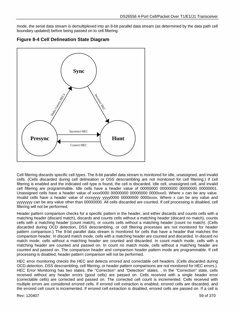
DS26556 4-Port Cell/Packet Over T1/E1/J1 Transceiver
Rev: 120407 59 of 370
mode, the serial data stream is demultiplexed into an 8-bit parallel data stream (as determined by the data path cell boundary updated) before being passed on to cell filtering.
Figure 8-4 Cell Delineation State Diagram
Sync
HuntPresyncIncorrect HEC
Correct HEC
Delta
Cor
rect
HECs
Incorrect HEC
Cell filtering discards specific cell types. The 8-bit parallel data stream is monitored for idle, unassigned, and invalid cells. (Cells discarded during cell delineation or DSS descrambling are not monitored for cell filtering.) If cell filtering is enabled and the indicated cell type is found, the cell is discarded. Idle cell, unassigned cell, and invalid cell filtering are programmable. Idle cells have a header value of 00000000 00000000 00000000 00000001. Unassigned cells have a header value of xxxx0000 00000000 00000000 0000xxx0. Where x can be any value. Invalid cells have a header value of xxxxyyyy yyyy0000 00000000 0000xxxx. Where x can be any value and yyyyyyyy can be any value other than 00000000. All cells discarded are counted. If cell processing is disabled, cell filtering will not be performed.
Header pattern comparison checks for a specific pattern in the header, and either discards and counts cells with a matching header (discard match), discards and counts cells without a matching header (discard no match), counts cells with a matching header (count match), or counts cells without a matching header (count no match). (Cells discarded during OCD detection, DSS descrambling, or cell filtering processes are not monitored for header pattern comparison.) The 8-bit parallel data stream is monitored for cells that have a header that matches the comparison header. In discard match mode, cells with a matching header are counted and discarded. In discard no match mode, cells without a matching header are counted and discarded. In count match mode, cells with a matching header are counted and passed on. In count no match mode, cells without a matching header are counted and passed on. The comparison header and comparison header pattern mode are programmable. If cell processing is disabled, header pattern comparison will not be performed.
HEC error monitoring checks the HEC and detects errored and correctable cell headers. (Cells discarded during OCD detection, DSS descrambling, cell filtering, or header pattern comparisons are not monitored for HEC errors.). HEC Error Monitoring has two states, the "Correction" and "Detection" states. . In the “Correction” state, cells received without any header errors (good cells) are passed on. Cells received with a single header error (correctable cells) are corrected and passed on. The corrected cell count is incremented. Cells received with multiple errors are considered errored cells. If errored cell extraction is enabled, errored cells are discarded, and the errored cell count is incremented. If errored cell extraction is disabled, errored cells are passed on. If a cell is
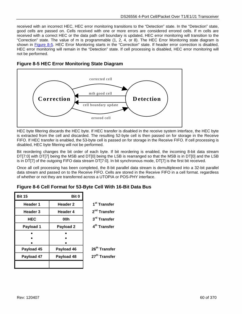
DS26556 4-Port Cell/Packet Over T1/E1/J1 Transceiver
Rev: 120407 60 of 370
received with an incorrect HEC, HEC error monitoring transitions to the “Detection” state. In the “Detection” state, good cells are passed on. Cells received with one or more errors are considered errored cells. If m cells are received with a correct HEC or the data path cell boundary is updated, HEC error monitoring will transition to the “Correction” state. The value of m is programmable (1, 2, 4, or 8). The HEC Error Monitoring state diagram is shown in Figure 8-5. HEC Error Monitoring starts in the “Correction” state. If header error correction is disabled, HEC error monitoring will remain in the “Detection” state. If cell processing is disabled, HEC error monitoring will not be performed.
Figure 8-5 HEC Error Monitoring State Diagram
D etectionC orrectionm th good cell
corrected cell
errored cell
cell boundary update
HEC byte filtering discards the HEC byte. If HEC transfer is disabled in the receive system interface, the HEC byte is extracted from the cell and discarded. The resulting 52-byte cell is then passed on for storage in the Receive FIFO. If HEC transfer is enabled, the 53-byte cell is passed on for storage in the Receive FIFO. If cell processing is disabled, HEC byte filtering will not be performed.
Bit reordering changes the bit order of each byte. If bit reordering is enabled, the incoming 8-bit data stream DT[7:0] with DT[7] being the MSB and DT[0] being the LSB is rearranged so that the MSB is in DT[0] and the LSB is in DT[7] of the outgoing FIFO data stream DT[7:0]. In bit synchronous mode, DT[7] is the first bit received.
Once all cell processing has been completed, the 8-bit parallel data stream is demultiplexed into a 32-bit parallel data stream and passed on to the Receive FIFO. Cells are stored in the Receive FIFO in a cell format. regardless of whether or not they are transferred across a UTOPIA or POS-PHY interface.
Figure 8-6 Cell Format for 53-Byte Cell With 16-Bit Data Bus
Bit 15 Bit 0
Header 1 Header 2 1st Transfer
Header 3 Header 4 2nd Transfer
HEC 00h 3rd Transfer
Payload 1 Payload 2 4th Transfer • • •
• • •
Payload 45 Payload 46 26th Transfer
Payload 47 Payload 48 27th Transfer
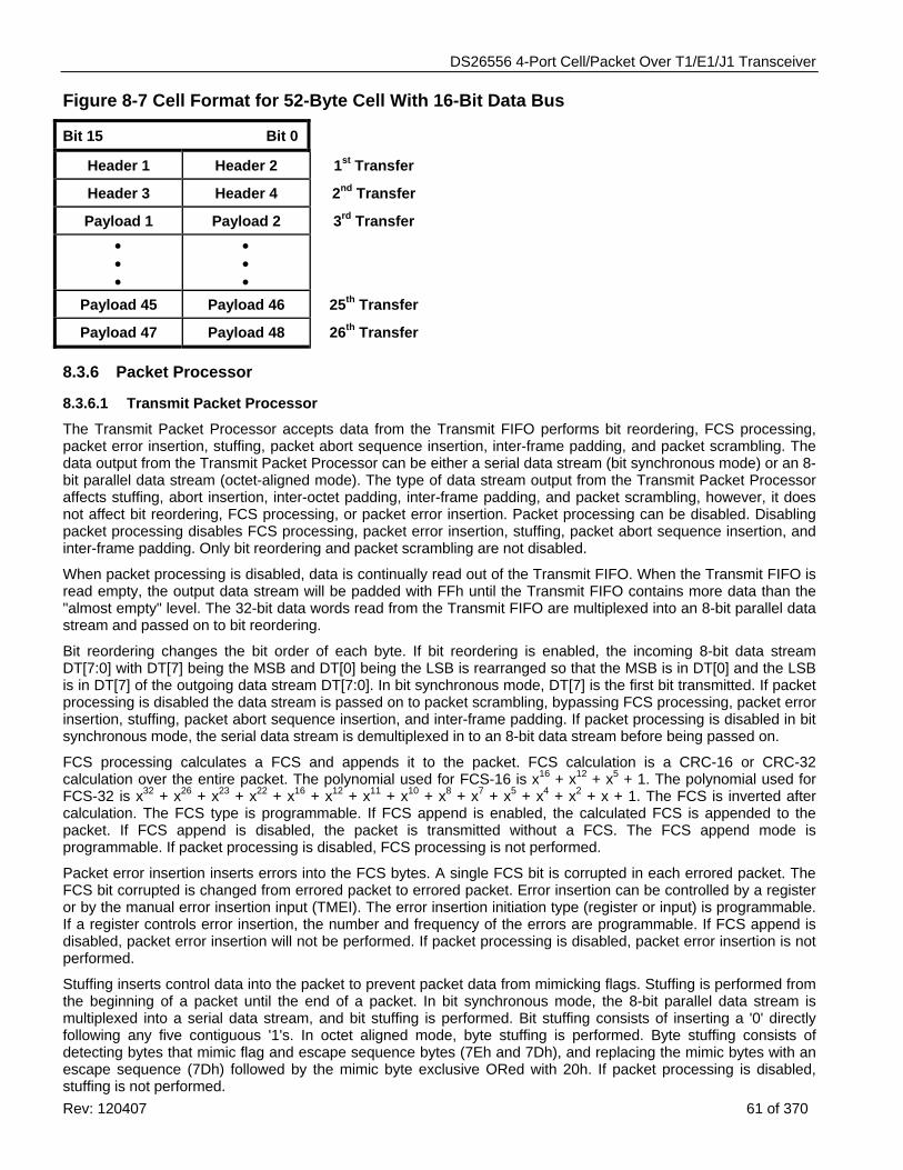
DS26556 4-Port Cell/Packet Over T1/E1/J1 Transceiver
Rev: 120407 61 of 370
Figure 8-7 Cell Format for 52-Byte Cell With 16-Bit Data Bus
Bit 15 Bit 0
Header 1 Header 2 1st Transfer
Header 3 Header 4 2nd Transfer
Payload 1 Payload 2 3rd Transfer • • •
• • •
Payload 45 Payload 46 25th Transfer
Payload 47 Payload 48 26th Transfer
8.3.6 Packet Processor
8.3.6.1 Transmit Packet Processor
The Transmit Packet Processor accepts data from the Transmit FIFO performs bit reordering, FCS processing, packet error insertion, stuffing, packet abort sequence insertion, inter-frame padding, and packet scrambling. The data output from the Transmit Packet Processor can be either a serial data stream (bit synchronous mode) or an 8-bit parallel data stream (octet-aligned mode). The type of data stream output from the Transmit Packet Processor affects stuffing, abort insertion, inter-octet padding, inter-frame padding, and packet scrambling, however, it does not affect bit reordering, FCS processing, or packet error insertion. Packet processing can be disabled. Disabling packet processing disables FCS processing, packet error insertion, stuffing, packet abort sequence insertion, and inter-frame padding. Only bit reordering and packet scrambling are not disabled.
When packet processing is disabled, data is continually read out of the Transmit FIFO. When the Transmit FIFO is read empty, the output data stream will be padded with FFh until the Transmit FIFO contains more data than the "almost empty" level. The 32-bit data words read from the Transmit FIFO are multiplexed into an 8-bit parallel data stream and passed on to bit reordering.
Bit reordering changes the bit order of each byte. If bit reordering is enabled, the incoming 8-bit data stream DT[7:0] with DT[7] being the MSB and DT[0] being the LSB is rearranged so that the MSB is in DT[0] and the LSB is in DT[7] of the outgoing data stream DT[7:0]. In bit synchronous mode, DT[7] is the first bit transmitted. If packet processing is disabled the data stream is passed on to packet scrambling, bypassing FCS processing, packet error insertion, stuffing, packet abort sequence insertion, and inter-frame padding. If packet processing is disabled in bit synchronous mode, the serial data stream is demultiplexed in to an 8-bit data stream before being passed on.
FCS processing calculates a FCS and appends it to the packet. FCS calculation is a CRC-16 or CRC-32 calculation over the entire packet. The polynomial used for FCS-16 is x16 + x12 + x5 + 1. The polynomial used for FCS-32 is x32 + x26 + x23 + x22 + x16 + x12 + x11 + x10 + x8 + x7 + x5 + x4 + x2 + x + 1. The FCS is inverted after calculation. The FCS type is programmable. If FCS append is enabled, the calculated FCS is appended to the packet. If FCS append is disabled, the packet is transmitted without a FCS. The FCS append mode is programmable. If packet processing is disabled, FCS processing is not performed.
Packet error insertion inserts errors into the FCS bytes. A single FCS bit is corrupted in each errored packet. The FCS bit corrupted is changed from errored packet to errored packet. Error insertion can be controlled by a register or by the manual error insertion input (TMEI). The error insertion initiation type (register or input) is programmable. If a register controls error insertion, the number and frequency of the errors are programmable. If FCS append is disabled, packet error insertion will not be performed. If packet processing is disabled, packet error insertion is not performed.
Stuffing inserts control data into the packet to prevent packet data from mimicking flags. Stuffing is performed from the beginning of a packet until the end of a packet. In bit synchronous mode, the 8-bit parallel data stream is multiplexed into a serial data stream, and bit stuffing is performed. Bit stuffing consists of inserting a '0' directly following any five contiguous '1's. In octet aligned mode, byte stuffing is performed. Byte stuffing consists of detecting bytes that mimic flag and escape sequence bytes (7Eh and 7Dh), and replacing the mimic bytes with an escape sequence (7Dh) followed by the mimic byte exclusive ORed with 20h. If packet processing is disabled, stuffing is not performed.
DS26556 4-Port Cell/Packet Over T1/E1/J1 Transceiver
Rev: 120407 62 of 370
Inter-frame padding inserts start flags, end flags and inter-frame fill between packets. There will be at least one flag plus a programmable number of additional flags between packets. In octet aligned mode, the inter-frame fill is flags. In bit synchronous mode, the inter-frame fill can be flags or all 1s followed by a start flag. If the inter-frame fill is all '1's, the number of '1's between the end and start flags may not be an integer number of bytes, however, there will be at least 15 consecutive '1's between the end and start flags. The bit synchronous mode inter-frame padding type is programmable. If packet processing is disabled, inter-frame padding is not performed.
Packet abort insertion inserts a packet abort sequences as necessary. If a packet abort indication is detected, a packet abort sequence is inserted and inter-frame padding is done until a packet start flag is detected. In bit synchronous mode, the abort sequence is FFh. In octet aligned mode, the abort sequence is 7D7Eh. If packet processing is disabled, packet abort insertion is not performed.
The packet scrambler is a x43 + 1 self-synchronous scrambler that scrambles the entire packet data stream. Packet scrambling is programmable.
Once all packet processing has been completed, in bit synchronous mode, the 8-bit parallel data stream is multiplexed into a serial data stream and passed on. In octet aligned mode, the 8-bit parallel data stream is passed on.
8.3.6.2 Receive Packet Processor
The Receive Packet Processor performs packet descrambling, packet delineation, inter-frame fill filtering, packet abort detection, destuffing, packet size checking, FCS error monitoring, FCS byte extraction, and bit reordering. The data coming in can be either a serial data stream or an 8-bit parallel data stream, depending on the framing mode The type of data stream received affects packet descrambling, packet delineation, inter-frame fill filtering, packet abort detection, and destuffing, however, it does not affect packet size checking, FCS error monitoring, FCS byte extraction, or bit reordering. Packet processing can be disabled (clear-channel enable). Disabling packet processing disables packet delineation, inter-frame fill filtering, packet abort detection, destuffing, packet size checking, FCS error monitoring, and FCS byte extraction. Only packet descrambling and bit reordering are not disabled.
The packet descrambler is a self-synchronous x43 + 1 descrambler that descrambles the entire packet data stream. Packet descrambling is programmable. If packet processing is disabled in bit synchronous mode, the serial data stream is demultiplexed in to an 8-bit data stream before being passed on.
If packet processing is disabled, a packet boundary is arbitrarily chosen, and the data is divided into "packets" whose size is programmable (maximum packet size setting). These packets are then passed on to bit reordering bypassing packet delineation, inter-frame fill filtering, packet abort detection, destuffing, packet size checking, FCS error monitoring, and FCS byte extraction.
Packet delineation determines the packet boundary by identifying a packet start or end flag. Each time slot is checked for a flag sequence (7Eh). Once a flag is found, it is identified as a start or end flag, and the packet boundary is set. If packet processing is disabled, packet delineation is not performed.
Inter-frame fill filtering removes the inter-frame fill between packets. When a packet end flag is detected, all data is discarded until a packet start flag is detected. In bit synchronous mode, the inter-frame fill can be flags or all '1's. When the interframe fill is all ‘1’s, the number of '1's between the start and end flags does not need to be an integer number of bytes. In bit synchronous mode when inter-frame fill is flags, there may be only one flag between packets, or the flags may have a shared zero (011111101111110). In octet aligned mode, the inter-frame fill can only be flags, and there may be only one flag between packets. If packet processing is disabled, inter-frame fill filtering is not performed.
Packet abort detection searches for a packet abort sequence. Between a packet start flag and a packet end flag, if an abort sequence is detected, the packet is marked with an abort indication, the aborted packet count is incremented, and all subsequent data is discarded until a packet start flag is detected. In bit synchronous mode, the abort sequence is seven consecutive ones. In octet aligned mode, the abort sequence is 7D7Eh. If packet processing is disabled, packet abort detection is not performed.
Destuffing removes the extra data inserted to prevent data from mimicking a flag or an abort sequence. In bit synchronous mode, bit destuffing is performed. Bit destuffing consists of discarding any '0' that directly follows five contiguous '1's. In octet aligned mode, byte destuffing is performed. Byte destuffing consists of detecting an escape sequence (7Dh), discarding it and exclusive ORing the next byte with 20h. In bit synchronous mode, after destuffing is completed, the serial bit stream is demultiplexed into an 8-bit parallel data stream and passed on to packet size checking. If there is less than eight bits in the last byte, an invalid packet flag is raised, the packet is
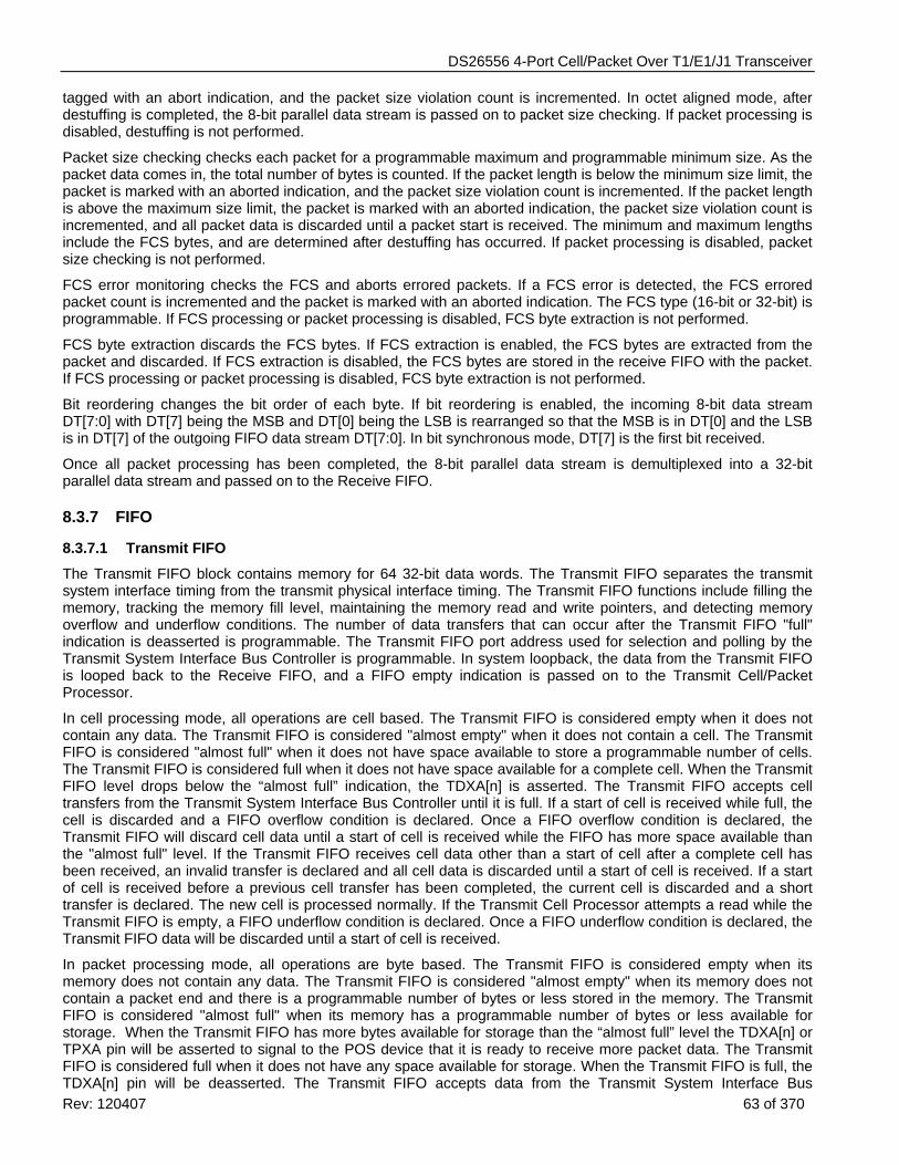
DS26556 4-Port Cell/Packet Over T1/E1/J1 Transceiver
Rev: 120407 63 of 370
tagged with an abort indication, and the packet size violation count is incremented. In octet aligned mode, after destuffing is completed, the 8-bit parallel data stream is passed on to packet size checking. If packet processing is disabled, destuffing is not performed.
Packet size checking checks each packet for a programmable maximum and programmable minimum size. As the packet data comes in, the total number of bytes is counted. If the packet length is below the minimum size limit, the packet is marked with an aborted indication, and the packet size violation count is incremented. If the packet length is above the maximum size limit, the packet is marked with an aborted indication, the packet size violation count is incremented, and all packet data is discarded until a packet start is received. The minimum and maximum lengths include the FCS bytes, and are determined after destuffing has occurred. If packet processing is disabled, packet size checking is not performed.
FCS error monitoring checks the FCS and aborts errored packets. If a FCS error is detected, the FCS errored packet count is incremented and the packet is marked with an aborted indication. The FCS type (16-bit or 32-bit) is programmable. If FCS processing or packet processing is disabled, FCS byte extraction is not performed.
FCS byte extraction discards the FCS bytes. If FCS extraction is enabled, the FCS bytes are extracted from the packet and discarded. If FCS extraction is disabled, the FCS bytes are stored in the receive FIFO with the packet. If FCS processing or packet processing is disabled, FCS byte extraction is not performed.
Bit reordering changes the bit order of each byte. If bit reordering is enabled, the incoming 8-bit data stream DT[7:0] with DT[7] being the MSB and DT[0] being the LSB is rearranged so that the MSB is in DT[0] and the LSB is in DT[7] of the outgoing FIFO data stream DT[7:0]. In bit synchronous mode, DT[7] is the first bit received.
Once all packet processing has been completed, the 8-bit parallel data stream is demultiplexed into a 32-bit parallel data stream and passed on to the Receive FIFO.
8.3.7 FIFO
8.3.7.1 Transmit FIFO
The Transmit FIFO block contains memory for 64 32-bit data words. The Transmit FIFO separates the transmit system interface timing from the transmit physical interface timing. The Transmit FIFO functions include filling the memory, tracking the memory fill level, maintaining the memory read and write pointers, and detecting memory overflow and underflow conditions. The number of data transfers that can occur after the Transmit FIFO "full" indication is deasserted is programmable. The Transmit FIFO port address used for selection and polling by the Transmit System Interface Bus Controller is programmable. In system loopback, the data from the Transmit FIFO is looped back to the Receive FIFO, and a FIFO empty indication is passed on to the Transmit Cell/Packet Processor.
In cell processing mode, all operations are cell based. The Transmit FIFO is considered empty when it does not contain any data. The Transmit FIFO is considered "almost empty" when it does not contain a cell. The Transmit FIFO is considered "almost full" when it does not have space available to store a programmable number of cells. The Transmit FIFO is considered full when it does not have space available for a complete cell. When the Transmit FIFO level drops below the “almost full” indication, the TDXA[n] is asserted. The Transmit FIFO accepts cell transfers from the Transmit System Interface Bus Controller until it is full. If a start of cell is received while full, the cell is discarded and a FIFO overflow condition is declared. Once a FIFO overflow condition is declared, the Transmit FIFO will discard cell data until a start of cell is received while the FIFO has more space available than the "almost full" level. If the Transmit FIFO receives cell data other than a start of cell after a complete cell has been received, an invalid transfer is declared and all cell data is discarded until a start of cell is received. If a start of cell is received before a previous cell transfer has been completed, the current cell is discarded and a short transfer is declared. The new cell is processed normally. If the Transmit Cell Processor attempts a read while the Transmit FIFO is empty, a FIFO underflow condition is declared. Once a FIFO underflow condition is declared, the Transmit FIFO data will be discarded until a start of cell is received.
In packet processing mode, all operations are byte based. The Transmit FIFO is considered empty when its memory does not contain any data. The Transmit FIFO is considered "almost empty" when its memory does not contain a packet end and there is a programmable number of bytes or less stored in the memory. The Transmit FIFO is considered "almost full" when its memory has a programmable number of bytes or less available for storage. When the Transmit FIFO has more bytes available for storage than the “almost full” level the TDXA[n] or TPXA pin will be asserted to signal to the POS device that it is ready to receive more packet data. The Transmit FIFO is considered full when it does not have any space available for storage. When the Transmit FIFO is full, the TDXA[n] pin will be deasserted. The Transmit FIFO accepts data from the Transmit System Interface Bus
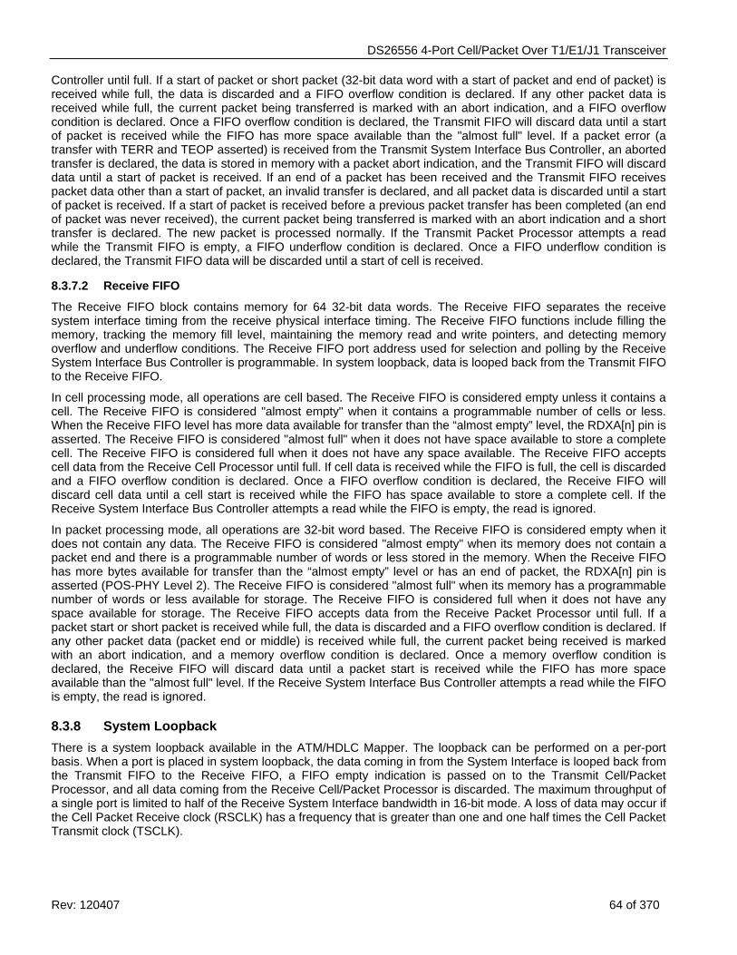
DS26556 4-Port Cell/Packet Over T1/E1/J1 Transceiver
Rev: 120407 64 of 370
Controller until full. If a start of packet or short packet (32-bit data word with a start of packet and end of packet) is received while full, the data is discarded and a FIFO overflow condition is declared. If any other packet data is received while full, the current packet being transferred is marked with an abort indication, and a FIFO overflow condition is declared. Once a FIFO overflow condition is declared, the Transmit FIFO will discard data until a start of packet is received while the FIFO has more space available than the "almost full" level. If a packet error (a transfer with TERR and TEOP asserted) is received from the Transmit System Interface Bus Controller, an aborted transfer is declared, the data is stored in memory with a packet abort indication, and the Transmit FIFO will discard data until a start of packet is received. If an end of a packet has been received and the Transmit FIFO receives packet data other than a start of packet, an invalid transfer is declared, and all packet data is discarded until a start of packet is received. If a start of packet is received before a previous packet transfer has been completed (an end of packet was never received), the current packet being transferred is marked with an abort indication and a short transfer is declared. The new packet is processed normally. If the Transmit Packet Processor attempts a read while the Transmit FIFO is empty, a FIFO underflow condition is declared. Once a FIFO underflow condition is declared, the Transmit FIFO data will be discarded until a start of cell is received.
8.3.7.2 Receive FIFO
The Receive FIFO block contains memory for 64 32-bit data words. The Receive FIFO separates the receive system interface timing from the receive physical interface timing. The Receive FIFO functions include filling the memory, tracking the memory fill level, maintaining the memory read and write pointers, and detecting memory overflow and underflow conditions. The Receive FIFO port address used for selection and polling by the Receive System Interface Bus Controller is programmable. In system loopback, data is looped back from the Transmit FIFO to the Receive FIFO.
In cell processing mode, all operations are cell based. The Receive FIFO is considered empty unless it contains a cell. The Receive FIFO is considered "almost empty" when it contains a programmable number of cells or less. When the Receive FIFO level has more data available for transfer than the “almost empty” level, the RDXA[n] pin is asserted. The Receive FIFO is considered "almost full" when it does not have space available to store a complete cell. The Receive FIFO is considered full when it does not have any space available. The Receive FIFO accepts cell data from the Receive Cell Processor until full. If cell data is received while the FIFO is full, the cell is discarded and a FIFO overflow condition is declared. Once a FIFO overflow condition is declared, the Receive FIFO will discard cell data until a cell start is received while the FIFO has space available to store a complete cell. If the Receive System Interface Bus Controller attempts a read while the FIFO is empty, the read is ignored.
In packet processing mode, all operations are 32-bit word based. The Receive FIFO is considered empty when it does not contain any data. The Receive FIFO is considered "almost empty" when its memory does not contain a packet end and there is a programmable number of words or less stored in the memory. When the Receive FIFO has more bytes available for transfer than the “almost empty” level or has an end of packet, the RDXA[n] pin is asserted (POS-PHY Level 2). The Receive FIFO is considered "almost full" when its memory has a programmable number of words or less available for storage. The Receive FIFO is considered full when it does not have any space available for storage. The Receive FIFO accepts data from the Receive Packet Processor until full. If a packet start or short packet is received while full, the data is discarded and a FIFO overflow condition is declared. If any other packet data (packet end or middle) is received while full, the current packet being received is marked with an abort indication, and a memory overflow condition is declared. Once a memory overflow condition is declared, the Receive FIFO will discard data until a packet start is received while the FIFO has more space available than the "almost full" level. If the Receive System Interface Bus Controller attempts a read while the FIFO is empty, the read is ignored.
8.3.8 System Loopback There is a system loopback available in the ATM/HDLC Mapper. The loopback can be performed on a per-port basis. When a port is placed in system loopback, the data coming in from the System Interface is looped back from the Transmit FIFO to the Receive FIFO, a FIFO empty indication is passed on to the Transmit Cell/Packet Processor, and all data coming from the Receive Cell/Packet Processor is discarded. The maximum throughput of a single port is limited to half of the Receive System Interface bandwidth in 16-bit mode. A loss of data may occur if the Cell Packet Receive clock (RSCLK) has a frequency that is greater than one and one half times the Cell Packet Transmit clock (TSCLK).
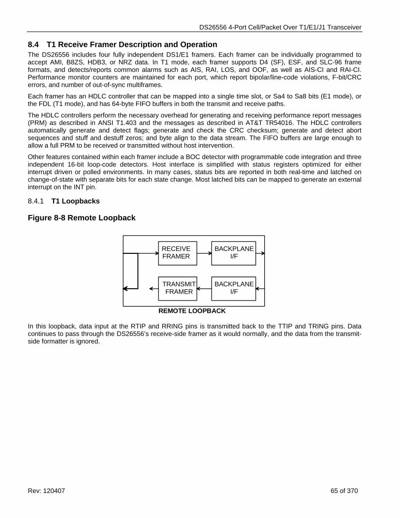
DS26556 4-Port Cell/Packet Over T1/E1/J1 Transceiver
Rev: 120407 65 of 370
8.4 T1 Receive Framer Description and Operation The DS26556 includes four fully independent DS1/E1 framers. Each framer can be individually programmed to accept AMI, B8ZS, HDB3, or NRZ data. In T1 mode, each framer supports D4 (SF), ESF, and SLC-96 frame formats, and detects/reports common alarms such as AIS, RAI, LOS, and OOF, as well as AIS-CI and RAI-CI. Performance monitor counters are maintained for each port, which report bipolar/line-code violations, F-bit/CRC errors, and number of out-of-sync multiframes.
Each framer has an HDLC controller that can be mapped into a single time slot, or Sa4 to Sa8 bits (E1 mode), or the FDL (T1 mode), and has 64-byte FIFO buffers in both the transmit and receive paths.
The HDLC controllers perform the necessary overhead for generating and receiving performance report messages (PRM) as described in ANSI T1.403 and the messages as described in AT&T TR54016. The HDLC controllers automatically generate and detect flags; generate and check the CRC checksum; generate and detect abort sequences and stuff and destuff zeros; and byte align to the data stream. The FIFO buffers are large enough to allow a full PRM to be received or transmitted without host intervention.
Other features contained within each framer include a BOC detector with programmable code integration and three independent 16-bit loop-code detectors. Host interface is simplified with status registers optimized for either interrupt driven or polled environments. In many cases, status bits are reported in both real-time and latched on change-of-state with separate bits for each state change. Most latched bits can be mapped to generate an external interrupt on the INT pin.
8.4.1 T1 Loopbacks
Figure 8-8 Remote Loopback
In this loopback, data input at the RTIP and RRING pins is transmitted back to the TTIP and TRING pins. Data continues to pass through the DS26556’s receive-side framer as it would normally, and the data from the transmit-side formatter is ignored.
REMOTE LOOPBACK
RECEIVEFRAMER
TRANSMITFRAMER
BACKPLANEI/F
BACKPLANEI/F
DS26556 4-Port Cell/Packet Over T1/E1/J1 Transceiver
Rev: 120407 66 of 370
Figure 8-9 Payload Loopback
When PLB is enabled, the following occurs: 1) Data is transmitted from the TTIP and TRING pins synchronous with RCLK instead of TCLK. 2) All the receive-side signals continue to operate normally. 3) TCHMKR is forced low. 4) Data at the TDATAI pin is ignored. Normally, this loopback is only enabled when ESF framing is being performed, but it can also be enabled in D4 framing applications. In a PLB situation, the DS26556 loops the 192 bits of payload data (with BPVs corrected) from the receive section back to the transmit section. The FPS framing pattern, CRC6 calculation, and the FDL bits are not looped back, they are reinserted by the DS26556.
Figure 8-10 Framer Loopback
This loopback is useful in testing and debugging applications. In FLB, the DS26556 loops data from the transmit side back to the receive side. When FLB is enabled, the following occurs: 1) (T1 mode) An unframed all-ones code is transmitted at TTIP and TRING.
(E1 mode) Normal data is transmitted at TTIP and TRING. 2) Data at RTIP and RRING is ignored. 3) All receive-side signals take on timing synchronous with TCLK instead of RCLK.
8.4.2 H.100 (CT Bus) Compatibility The H.100 (or CT Bus) is a synchronous, bit-serial, TDM transport bus operating at 8.192MHz. The H.100 standard also allows compatibility modes to operate at 2.048MHz, 4.096MHz, or 8.192MHz. The control bit, H100EN (RIOCR.5), when combined with HSSYNCINV, allows the DS26556 to accept a CT-Bus-compatible frame-sync signal (CT_FRAME) at the HSSYNC input. The following rules apply to the H100EN control bit: 1) The H100EN bit controls the sampling point for the HSSYNC input signal only.
PAYLOAD LOOPBACK(CAN BE DONE ON A PER-CHANNEL BASIS)
RECEIVEFRAMER
TRANSMITFRAMER
BACKPLANEI/F
BACKPLANEI/F
FRAMER LOOPBACK
RECEIVEFRAMER
TRANSMITFRAMER
BACKPLANEI/F
BACKPLANEI/F
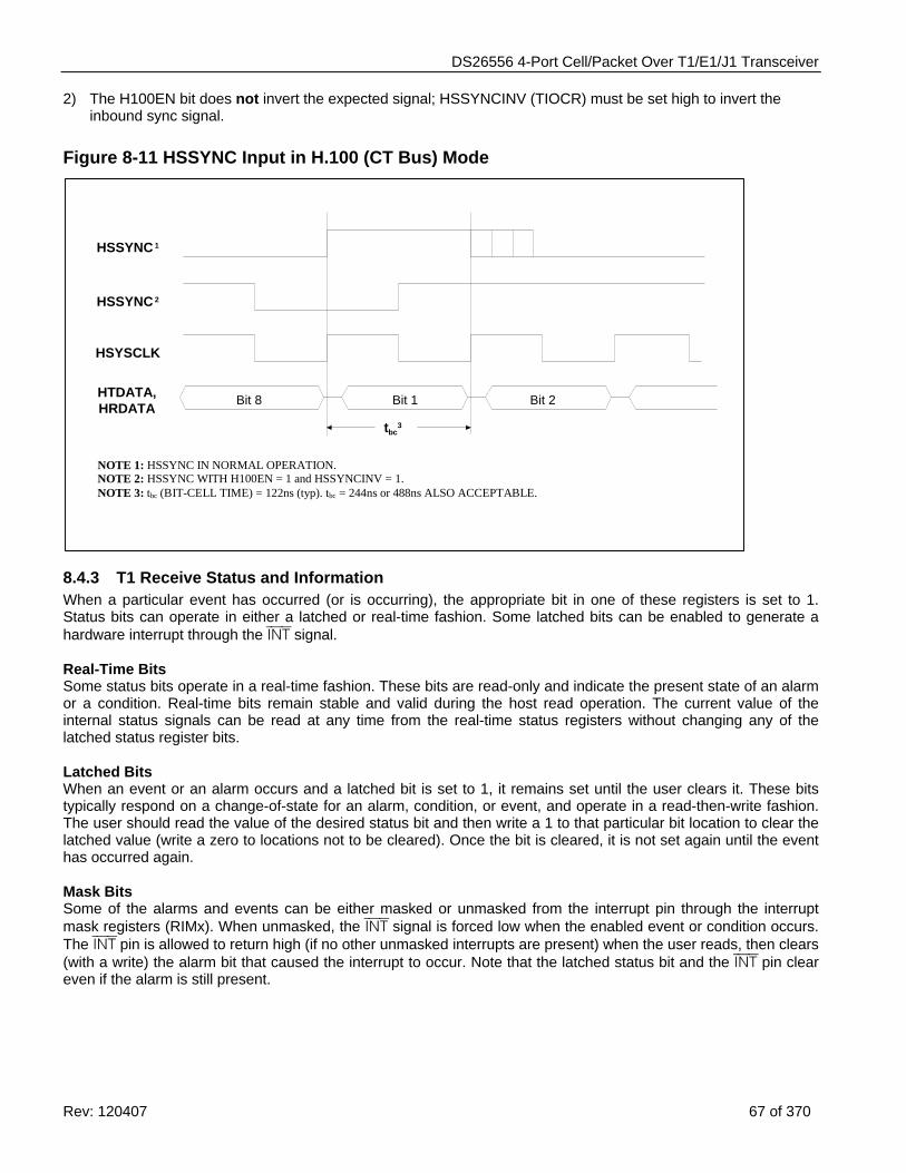
DS26556 4-Port Cell/Packet Over T1/E1/J1 Transceiver
Rev: 120407 67 of 370
2) The H100EN bit does not invert the expected signal; HSSYNCINV (TIOCR) must be set high to invert the inbound sync signal.
Figure 8-11 HSSYNC Input in H.100 (CT Bus) Mode
Bit 8 Bit 1 Bit 2
HSSYNC 1
HSSYNC 2
HSYSCLK
HTDATA,HRDATA
tbc3
NOTE 1: HSSYNC IN NORMAL OPERATION.NOTE 2: HSSYNC WITH H100EN = 1 and HSSYNCINV = 1.NOTE 3: tbc (BIT-CELL TIME) = 122ns (typ). tbc = 244ns or 488ns ALSO ACCEPTABLE.
8.4.3 T1 Receive Status and Information When a particular event has occurred (or is occurring), the appropriate bit in one of these registers is set to 1. Status bits can operate in either a latched or real-time fashion. Some latched bits can be enabled to generate a hardware interrupt through the INT signal. Real-Time Bits Some status bits operate in a real-time fashion. These bits are read-only and indicate the present state of an alarm or a condition. Real-time bits remain stable and valid during the host read operation. The current value of the internal status signals can be read at any time from the real-time status registers without changing any of the latched status register bits. Latched Bits When an event or an alarm occurs and a latched bit is set to 1, it remains set until the user clears it. These bits typically respond on a change-of-state for an alarm, condition, or event, and operate in a read-then-write fashion. The user should read the value of the desired status bit and then write a 1 to that particular bit location to clear the latched value (write a zero to locations not to be cleared). Once the bit is cleared, it is not set again until the event has occurred again. Mask Bits Some of the alarms and events can be either masked or unmasked from the interrupt pin through the interrupt mask registers (RIMx). When unmasked, the INT signal is forced low when the enabled event or condition occurs. The INT pin is allowed to return high (if no other unmasked interrupts are present) when the user reads, then clears (with a write) the alarm bit that caused the interrupt to occur. Note that the latched status bit and the INT pin clear even if the alarm is still present.
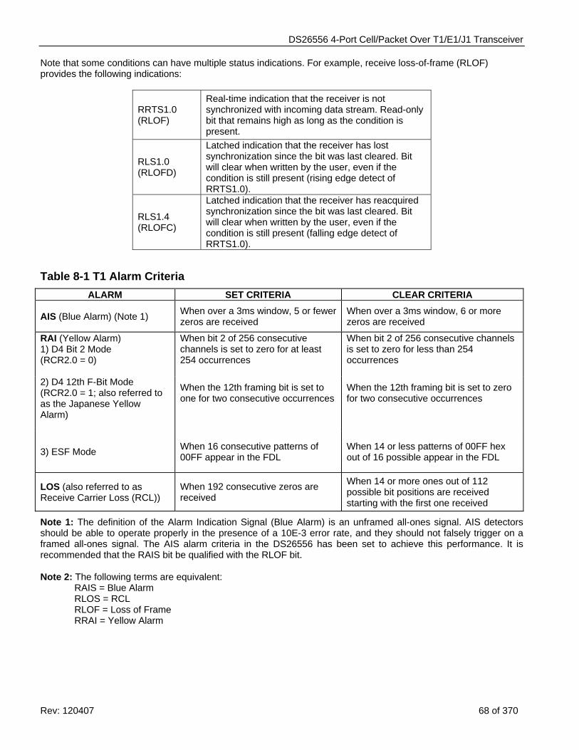
DS26556 4-Port Cell/Packet Over T1/E1/J1 Transceiver
Rev: 120407 68 of 370
Note that some conditions can have multiple status indications. For example, receive loss-of-frame (RLOF) provides the following indications:
RRTS1.0 (RLOF)
Real-time indication that the receiver is not synchronized with incoming data stream. Read-only bit that remains high as long as the condition is present.
RLS1.0 (RLOFD)
Latched indication that the receiver has lost synchronization since the bit was last cleared. Bit will clear when written by the user, even if the condition is still present (rising edge detect of RRTS1.0).
RLS1.4 (RLOFC)
Latched indication that the receiver has reacquired synchronization since the bit was last cleared. Bit will clear when written by the user, even if the condition is still present (falling edge detect of RRTS1.0).
Table 8-1 T1 Alarm Criteria ALARM SET CRITERIA CLEAR CRITERIA
AIS (Blue Alarm) (Note 1) When over a 3ms window, 5 or fewer zeros are received
When over a 3ms window, 6 or more zeros are received
RAI (Yellow Alarm) 1) D4 Bit 2 Mode (RCR2.0 = 0)
When bit 2 of 256 consecutive channels is set to zero for at least 254 occurrences
When bit 2 of 256 consecutive channels is set to zero for less than 254 occurrences
2) D4 12th F-Bit Mode (RCR2.0 = 1; also referred to as the Japanese Yellow Alarm)
When the 12th framing bit is set to one for two consecutive occurrences
When the 12th framing bit is set to zero for two consecutive occurrences
3) ESF Mode When 16 consecutive patterns of 00FF appear in the FDL
When 14 or less patterns of 00FF hex out of 16 possible appear in the FDL
LOS (also referred to as Receive Carrier Loss (RCL))
When 192 consecutive zeros are received
When 14 or more ones out of 112 possible bit positions are received starting with the first one received
Note 1: The definition of the Alarm Indication Signal (Blue Alarm) is an unframed all-ones signal. AIS detectors should be able to operate properly in the presence of a 10E-3 error rate, and they should not falsely trigger on a framed all-ones signal. The AIS alarm criteria in the DS26556 has been set to achieve this performance. It is recommended that the RAIS bit be qualified with the RLOF bit. Note 2: The following terms are equivalent:
RAIS = Blue Alarm RLOS = RCL RLOF = Loss of Frame RRAI = Yellow Alarm
DS26556 4-Port Cell/Packet Over T1/E1/J1 Transceiver
Rev: 120407 69 of 370
8.4.4 Receive AIS-CI and RAI-CI Detection AIS-CI is a repetitive pattern of 1.26 seconds. It consists of 1.11 seconds of an unframed all ones pattern and 0.15 seconds of all ones modified by the AIS-CI signature. The AIS-CI signature is a repetitive pattern 6176 bits in length in which, if the first bit is numbered bit 0, bits 3088, 3474 and 5790 are logical zeros and all other bits in the pattern are logical ones (T1.403). AIS-CI is an unframed pattern and therefore is defined for all T1 framing formats. The RAIS-CI bit is set when the AIS-CI pattern has been detected and RAIS (RRTS1.2) is set. RAIS-CI is a latched bit and should be cleared by the host when read. RAIS-CI will continue to set approximately every 1.2 seconds that the condition is present. The host will need to ‘poll’ the bit, in conjunction with the normal AIS indicators to determine when the condition has cleared.
RAI-CI is a repetitive pattern within the ESF data link with a period of 1.08 seconds. It consists of sequentially interleaving 0.99 seconds of “00000000 11111111” (right-to-left) with 90ms of “00111110 11111111”. The RRAI-CI bit is set when a bit-oriented code of “00111110 11111111” is detected while RRAI (RRTS1.3) is set. The RRAI-CI detector uses the receive BOC filter bits (RBF0 & RBF1) located in RBOCC to determine the integration time for RAI-CI detection. Like RAIS-CI, the RRAI-CI bit is latched and should be cleared by the host when read. RRAI-CI will continue to set approximately every 1.1 seconds that the condition is present. The host will need to ‘poll’ the bit, in conjunction with the normal RAI indicators to determine when the condition has cleared. It may be useful to enable the 200ms ESF RAI integration time with the RAIIE control bit (RCR2.1) in networks that use RAI-CI.
8.4.5 T1 Receive-Side Digital Milliwatt Code Generation Receive-side digital milliwatt code generation involves using the receive-digital milliwatt registers (T1RDMR1/2/3) to determine which of the 24 T1 channels of the T1 line going to the backplane should be overwritten with a digital milliwatt pattern. The digital milliwatt code is an 8-byte repeating pattern that represents a 1kHz sine wave (1E/0B/0B/1E/9E/8B/8B/9E). Each bit in the T1RDMRx registers, represents a particular channel. If a bit is set to 1, then the receive data in that channel is replaced with the digital milliwatt code. If a bit is set to zero, no replacement occurs.
8.4.6 T1 Error Count Registers The DS26556 contains three T1 performance counters that are used to accumulate line coding errors, path errors, and synchronization errors. Counter update options include one-second boundaries, 42ms (T1 mode only), 62.5ms (E1 mode only), or manually. See the Error Counter Configuration Register (ERCNT) section. When updated automatically, the user can use the interrupt from the timer to determine when to read these registers. The line-code violation count register has the potential to saturate, but the bit error would have to exceed 10E-2 before this would occur. All other counters roll over.
Several options are available for latching the performance counters:
1) Each framer’s counters are latched independently based on independent one-second interval timers. 2) Each framer’s counters are latched independently based on independent 42ms interval timers. 3) Each framer’s counters are latched independently with a low-to-high transition on the respective MECU control
bit. 4) Counters from selected framers are latched synchronously at the one-second interval supplied by Framer #1. 5) Counters from selected framers are synchronously latched manually with the global counter latch-enable
(GCLE) bit in GCR1.
The following table shows control bit settings in the ERCNT register to support each of the five modes discussed above.
Control Bit Mode 1 Mode 2 Mode 3 Mode 4 Mode 5 EAMS 0 0 1 0 1 ECUS 0 1 X 0 0 MECU 0 0 0 to 1 0 0 MCUS 0 0 0 0 1 1SECS 0 0 0 1 0
DS26556 4-Port Cell/Packet Over T1/E1/J1 Transceiver
Rev: 120407 70 of 370
8.4.7 T1 Receive Signaling Operation There are two methods of accessing receive-signaling data: through processor-based (i.e., software-based) signaling or hardware-based signaling. Processor-based refers to access through the receive-signaling registers, RS1 through RS12. Hardware-based refers to the HRSIG pin. Hardware based signaling is available only when the port is configured in the multiplexed bus mode utilizing the high speed TDM port. Both methods can be used simultaneously. NOTE: The receive framer does not normally remove robbed-bit signaling from the data stream. Signaling information is present in the data stream at the RSER pin unless the receive framer has been programmed to over-lay certain channels with idle codes or to force signaling bit positions to a “one” state. The signaling data in data stream at the HRDATA pin can be re-aligned to a users multiframe reference. See Signaling Re-insertion below.
8.4.8 Software Signaling Robbed-bit signaling (the LSB of each channel during frames 6, 12, 18 and 24 in ESF mode and frames 6 and 12 in D4 mode ) is sampled in the receive data stream and copied into the receive-signaling registers, RS1 through RS12. The signaling information in these registers is always updated on multiframe boundaries. This function is referred to as “Software Based Signaling” and is always enabled. The signaling bit position of each channels is sampled even thought the channel may not be carrying signaling information. The user may simply ignore these channels.
8.4.8.1 Change of State To avoid constant monitoring of the receive-signaling registers, the DS26556 can be programmed to alert the host when any specific channel or channels undergo a change of their signaling state. For T1, RSCSE1 through RSCSE3 are used to select which channels can cause a change-of-state indication. The change of state is indicated in latched status register 4 (RLS4.3). The user can enable the INT pin to toggle low upon detection of a change in signaling by setting the interrupt mask bit RIM4.3.
The user can identify which channels have undergone a signaling change of state by reading the receive-signaling status (RSS1–RSS3) registers. The information from these registers tells the user which RSx register to read for the new signaling data. All changes are indicated in the RSS1 through RSS3 registers regardless of the state of t he RSCSE1 through RSCSE3 registers.
8.4.9 Hardware Signaling A TDM signaling stream is available via the HRSIG pin when the port is configured to use the high speed multiplexed TDM bus. HRSIG is a signaling-PCM stream output on a channel-by-channel basis from the signaling buffer and multiplexed with any other port configured to use the high speed TDM bus. In ESF mode the HRSIG data is updated once a multiframe (3ms) unless a freeze is in effect. In the D4 framing mode, the AB signaling bits are output twice on RSIG in the lower nibble of each channel. Hence, bits 5 and 6 contain the same data as bits 7 and 8, respectively, in each channel. The HRSIG data is updated once a multiframe (1.5ms) unless a freeze is in effect.
8.4.9.1 Signaling Debounce When signaling integration is enabled (RSIGC.0 = 1), the signaling data at the HRSIG pin is automatically debounced. Signaling must be constant for three multiframes before being updated at HRSIG. Signaling debounce is enabled on a global basis (all channels or none). NOTE: This feature is available only on the high speed TDM bus.
8.4.10 Signaling Re-insertion The signaling buffer allows signaling data to be reinserted into the original data stream in a different alignment determined by a multiframe sync signal from the HSSYNC pin. Registers RSI1 through RSI4 are used to select signaling re-insertion on a channel-by-channel basis. Ports configured to be multiplexed on the high speed TDM bus can have the same signaling alignment. In T1 mode re-insertion generally results in there being two copies of robbed signaling for each port in the data stream, one at the original position and one at the user defined position. NOTE: It is possible to configure only one port to the high speed multiplexed bus. In this case the RSER pin for that port and the HRDATA pin are duplicates.
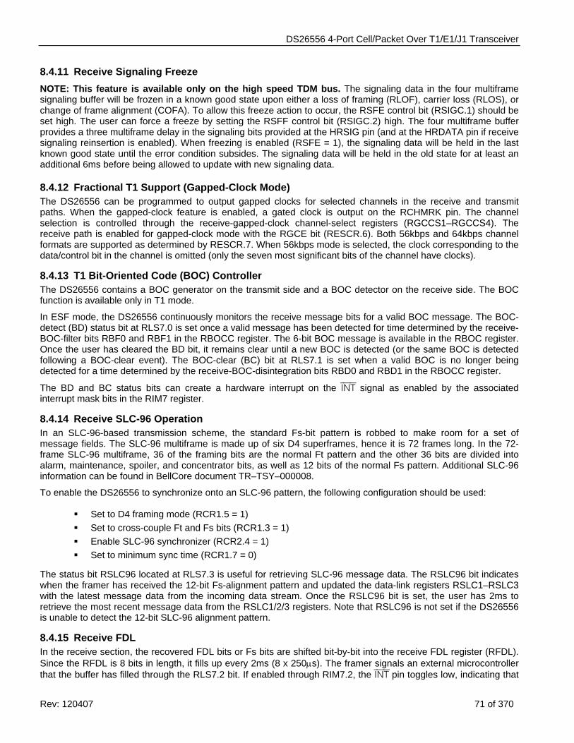
DS26556 4-Port Cell/Packet Over T1/E1/J1 Transceiver
Rev: 120407 71 of 370
8.4.11 Receive Signaling Freeze NOTE: This feature is available only on the high speed TDM bus. The signaling data in the four multiframe signaling buffer will be frozen in a known good state upon either a loss of framing (RLOF), carrier loss (RLOS), or change of frame alignment (COFA). To allow this freeze action to occur, the RSFE control bit (RSIGC.1) should be set high. The user can force a freeze by setting the RSFF control bit (RSIGC.2) high. The four multiframe buffer provides a three multiframe delay in the signaling bits provided at the HRSIG pin (and at the HRDATA pin if receive signaling reinsertion is enabled). When freezing is enabled (RSFE = 1), the signaling data will be held in the last known good state until the error condition subsides. The signaling data will be held in the old state for at least an additional 6ms before being allowed to update with new signaling data.
8.4.12 Fractional T1 Support (Gapped-Clock Mode) The DS26556 can be programmed to output gapped clocks for selected channels in the receive and transmit paths. When the gapped-clock feature is enabled, a gated clock is output on the RCHMRK pin. The channel selection is controlled through the receive-gapped-clock channel-select registers (RGCCS1–RGCCS4). The receive path is enabled for gapped-clock mode with the RGCE bit (RESCR.6). Both 56kbps and 64kbps channel formats are supported as determined by RESCR.7. When 56kbps mode is selected, the clock corresponding to the data/control bit in the channel is omitted (only the seven most significant bits of the channel have clocks).
8.4.13 T1 Bit-Oriented Code (BOC) Controller The DS26556 contains a BOC generator on the transmit side and a BOC detector on the receive side. The BOC function is available only in T1 mode.
In ESF mode, the DS26556 continuously monitors the receive message bits for a valid BOC message. The BOC-detect (BD) status bit at RLS7.0 is set once a valid message has been detected for time determined by the receive-BOC-filter bits RBF0 and RBF1 in the RBOCC register. The 6-bit BOC message is available in the RBOC register. Once the user has cleared the BD bit, it remains clear until a new BOC is detected (or the same BOC is detected following a BOC-clear event). The BOC-clear (BC) bit at RLS7.1 is set when a valid BOC is no longer being detected for a time determined by the receive-BOC-disintegration bits RBD0 and RBD1 in the RBOCC register.
The BD and BC status bits can create a hardware interrupt on the INT signal as enabled by the associated interrupt mask bits in the RIM7 register.
8.4.14 Receive SLC-96 Operation In an SLC-96-based transmission scheme, the standard Fs-bit pattern is robbed to make room for a set of message fields. The SLC-96 multiframe is made up of six D4 superframes, hence it is 72 frames long. In the 72-frame SLC-96 multiframe, 36 of the framing bits are the normal Ft pattern and the other 36 bits are divided into alarm, maintenance, spoiler, and concentrator bits, as well as 12 bits of the normal Fs pattern. Additional SLC-96 information can be found in BellCore document TR–TSY–000008.
To enable the DS26556 to synchronize onto an SLC-96 pattern, the following configuration should be used:
Set to D4 framing mode (RCR1.5 = 1) Set to cross-couple Ft and Fs bits (RCR1.3 = 1) Enable SLC-96 synchronizer (RCR2.4 = 1) Set to minimum sync time (RCR1.7 = 0)
The status bit RSLC96 located at RLS7.3 is useful for retrieving SLC-96 message data. The RSLC96 bit indicates when the framer has received the 12-bit Fs-alignment pattern and updated the data-link registers RSLC1–RSLC3 with the latest message data from the incoming data stream. Once the RSLC96 bit is set, the user has 2ms to retrieve the most recent message data from the RSLC1/2/3 registers. Note that RSLC96 is not set if the DS26556 is unable to detect the 12-bit SLC-96 alignment pattern.
8.4.15 Receive FDL In the receive section, the recovered FDL bits or Fs bits are shifted bit-by-bit into the receive FDL register (RFDL). Since the RFDL is 8 bits in length, it fills up every 2ms (8 x 250μs). The framer signals an external microcontroller that the buffer has filled through the RLS7.2 bit. If enabled through RIM7.2, the INT pin toggles low, indicating that
DS26556 4-Port Cell/Packet Over T1/E1/J1 Transceiver
Rev: 120407 72 of 370
the buffer has filled and needs to be read. The user has 2ms to read this data before it is lost. Note that no zero destuffing is applied for the data provided through the RFDL register.
8.4.16 Programmable In-Band Loop-Code Detection The DS26556 can generate and detect a repeating bit pattern from 1 to 8 bits or 16 bits in length. This function is available only in T1 mode. The framer has three programmable pattern detectors. Typically, two of the detectors are used for loop-up and loop-down code detection. The user programs the codes to be detected in the receive-up-code definition (RUPCD1 and RUPCD2) registers and the receive-down-code definition (RDNCD1 and RDNCD2) registers, and the length of each pattern is selected through the RIBCC register. A third detector (spare) is defined and controlled through the RSPCD1/RSPCD2 and RSCC registers. When detecting a 16-bit pattern, both receive-code-definition registers are used together to form a 16-bit register. For 8-bit patterns, both receive-code-definition registers are filled with the same value. Detection of a 1-, 2-, 3-, 4-, 5-, 6-, and 7-bit pattern only requires the first receive-code-definition register to be filled. The framer detects repeating pattern codes in framed and unframed circumstances with bit-error rates as high as 10E-2. The detectors can handle F-bit-inserted and F-bit-overwrite patterns. Writing the least significant byte of the receive-code-definition register resets the integration period for that detector. The code detector has a nominal integration period of 36ms. Therefore, after about 36ms of receiving a valid code, the proper status bit (LUP, LDN, and LSP) is set to 1. Note that real-time status bits, as well as latched set and clear bits, are available for LUP, LDN, and LSP (RRTS3 and RLS3). Normally codes are sent for 5 seconds. It is recommended that the software poll the framer every 50ms to 1000ms until 5 seconds has elapsed to ensure the code is continuously present.
8.4.17 Receive HDLC Controller The HDLC controller can be mapped into a single time slot, or Sa4 to Sa8 bits (E1 mode), or the FDL (T1 mode). The HDLC controller has a 64-byte FIFO buffer in the transmit and receive paths. The user can select any specific bits within the time slot(s) to assign to the HDLC controller, as well as specific Sa bits (E1 mode).
The HDLC controller performs the necessary overhead for generating and receiving performance report messages (PRM) as described in ANSI T1.403 and the messages as described in AT&T TR54016. The HDLC controller automatically generates and detects flags; generates and checks the CRC checksum; generates and detects abort sequences and stuffs and destuffs zeros; and byte aligns to the data stream. The 64-byte buffers in the HDLC controller are large enough to allow a full PRM to be received or transmitted without host intervention.
DS26556 4-Port Cell/Packet Over T1/E1/J1 Transceiver
Rev: 120407 73 of 370
8.4.18 Receive HDLC Controller Example The HDLC status registers in the DS26556 allow for flexible software interface to meet the user’s preferences. When receiving HDLC messages, the host can choose to be interrupt-driven, or to poll to desired status registers, or a combination of polling and interrupt processes can be used. shows an example routine for using the DS26556 HDLC receiver.
Figure 8-12 Receive HDLC Example
Reset Receive HDLC Controller
(RHC.6)
Configure Receive HDLC Controller
(RHC, RHBSE, RHFC)
Start NewMessage Buffer
Enable InterruptsRPE and RHWM
Start NewMessage Buffer
Interrupt?
Read Register RHPBA
Read N Bytes From Rx HDLC FIFO (RHF)
N = RHPBA[5..0]
MS = 0?(MS = RHPBA[7])
NO
YES
NO
YES
Read RRTS5 for Packet Status (PS2..0)Take appropriate action
No Action RequiredWork Another Process
DS26556 4-Port Cell/Packet Over T1/E1/J1 Transceiver
Rev: 120407 74 of 370
8.5 T1 Transmit Formatter Description and Operation Four fully independent DS1/E1 transmit formatters are included within the DS26556. Each port can be individually programmed to transmit AMI, B8ZS, HDB3, or NRZ data. In T1 mode each formatter supports D4 (SF), ESF, and SLC-96 frame formats, and transmits common alarms such as AIS, RAI, AIS-CI, and RAI-CI.
Each framer also has an HDLC controller which can be mapped into a single time slot, or Sa4 to Sa8 bits (E1 Mode) or the FDL (T1 Mode) and has 64 byte FIFO buffers in both the transmit and receive paths. The user can select any specific bits within the time slot(s) to assign to the HDLC controllers, as well as specific Sa bits (E1 Mode).
The HDLC controllers perform all the necessary overhead for generating and receiving Performance Report Messages (PRM) as described in ANSI T1.403 and the messages as described in AT&T TR54016. The controllers automatically generate and detects flags, generate and check the CRC check sum, generate and detect abort sequences, stuff and de-stuff zeros, and byte align to the data stream. The large FIFO buffers allow a full PRM to be received or transmitted without host intervention.
Other features contained within each framer include a BOC generator and a 16-bit loop code generator. Host interface is simplified with status registers optimized for either interrupt driven or polled environments. In many cases, status bits are reported both real-time and latched on change-of-state with separate bits for each state change. Most latched bits can be enabled to generate an external interrupt on the INT pin.
Additional details concerning the operation of the DS1 formatter are included within the register descriptions within this section.
8.5.1 T1 Per-Channel Loopback The Per-Channel Loopback Registers (PCLRs) determine which channels (if any) from the backplane should be replaced with the data from the receive side or in other words, off of the T1 or E1 line. If this loopback is enabled, then transmit and receive clocks and frame syncs must be synchronized. One method to accomplish this would be to tie RCLK to TCLK and RFSYNC to TSYNC. There are no restrictions on which channels can be looped back or on how many channels can be looped back.
8.5.2 T1 Transmit DS0 Monitoring Function The DS26556 has the ability to monitor one DS0 (64kbps) channel in the transmit direction and one DS0 channel in the receive direction at the same time. In the transmit direction the user will determine which channel is to be monitored by properly setting the TCM0 to TCM4 bits in the TDS0SEL register. In the receive direction, the RCM0 to RCM4 bits in the RDS0SEL register need to be properly set. The DS0 channel pointed to by the TCM0 to TCM4 bits will appear in the Transmit DS0 Monitor (TDS0M) register and the DS0 channel pointed to by the RCM0 to RCM4 bits will appear in the Receive DS0 (RDS0M) register. The TCM4 to TCM0 and RCM4 to RCM0 bits should be programmed with the decimal decode of the appropriate T1or E1 channel. T1 channels 1 through 24 map to register values 0 through 23. E1 channels 1 through 32 map to register values 0 through 31. For example, if DS0 channel 6 in the transmit direction and DS0 channel 15 in the receive direction needed to be monitored, then the following values would be programmed into TDS0SEL and RDS0SEL:
TCM[4:0] = 00101 RCM[4:0] = 01110
8.5.3 T1 Transmit Signaling Operation There are two methods of providing transmit signaling data—processor-based (i.e., software-based) or hardware-based. Processor-based refers to access through the transmit signaling registers, TS1 through TS12, while hardware-based refers to using the HTSIG pins. Hardware based signaling is available only when the port is configured in the multiplexed bus mode utilizing the high speed TDM port. Both methods can be used simultaneously. Note: Signaling data may already be imbedded in the transmit data streams at the TSER or HTDATA pins. In this case the two methods mentioned above may be used to update any or all channels.
8.5.3.1 Software Signaling Signaling data is loaded into the Transmit Signaling registers (TS1–TS12) via the host interface. On multiframe boundaries, the contents of these registers are loaded into a shift register for placement in the appropriate bit position in the outgoing data stream. The user can utilize the Transmit Multiframe Interrupt in Latched Status
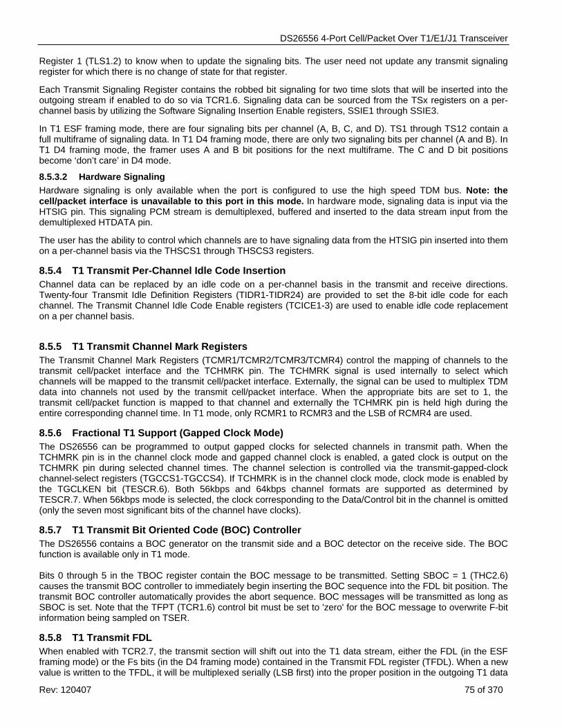
DS26556 4-Port Cell/Packet Over T1/E1/J1 Transceiver
Rev: 120407 75 of 370
Register 1 (TLS1.2) to know when to update the signaling bits. The user need not update any transmit signaling register for which there is no change of state for that register.
Each Transmit Signaling Register contains the robbed bit signaling for two time slots that will be inserted into the outgoing stream if enabled to do so via TCR1.6. Signaling data can be sourced from the TSx registers on a per-channel basis by utilizing the Software Signaling Insertion Enable registers, SSIE1 through SSIE3.
In T1 ESF framing mode, there are four signaling bits per channel (A, B, C, and D). TS1 through TS12 contain a full multiframe of signaling data. In T1 D4 framing mode, there are only two signaling bits per channel (A and B). In T1 D4 framing mode, the framer uses A and B bit positions for the next multiframe. The C and D bit positions become ‘don’t care’ in D4 mode.
8.5.3.2 Hardware Signaling Hardware signaling is only available when the port is configured to use the high speed TDM bus. Note: the cell/packet interface is unavailable to this port in this mode. In hardware mode, signaling data is input via the HTSIG pin. This signaling PCM stream is demultiplexed, buffered and inserted to the data stream input from the demultiplexed HTDATA pin.
The user has the ability to control which channels are to have signaling data from the HTSIG pin inserted into them on a per-channel basis via the THSCS1 through THSCS3 registers.
8.5.4 T1 Transmit Per-Channel Idle Code Insertion Channel data can be replaced by an idle code on a per-channel basis in the transmit and receive directions. Twenty-four Transmit Idle Definition Registers (TIDR1-TIDR24) are provided to set the 8-bit idle code for each channel. The Transmit Channel Idle Code Enable registers (TCICE1-3) are used to enable idle code replacement on a per channel basis.
8.5.5 T1 Transmit Channel Mark Registers The Transmit Channel Mark Registers (TCMR1/TCMR2/TCMR3/TCMR4) control the mapping of channels to the transmit cell/packet interface and the TCHMRK pin. The TCHMRK signal is used internally to select which channels will be mapped to the transmit cell/packet interface. Externally, the signal can be used to multiplex TDM data into channels not used by the transmit cell/packet interface. When the appropriate bits are set to 1, the transmit cell/packet function is mapped to that channel and externally the TCHMRK pin is held high during the entire corresponding channel time. In T1 mode, only RCMR1 to RCMR3 and the LSB of RCMR4 are used.
8.5.6 Fractional T1 Support (Gapped Clock Mode) The DS26556 can be programmed to output gapped clocks for selected channels in transmit path. When the TCHMRK pin is in the channel clock mode and gapped channel clock is enabled, a gated clock is output on the TCHMRK pin during selected channel times. The channel selection is controlled via the transmit-gapped-clock channel-select registers (TGCCS1-TGCCS4). If TCHMRK is in the channel clock mode, clock mode is enabled by the TGCLKEN bit (TESCR.6). Both 56kbps and 64kbps channel formats are supported as determined by TESCR.7. When 56kbps mode is selected, the clock corresponding to the Data/Control bit in the channel is omitted (only the seven most significant bits of the channel have clocks).
8.5.7 T1 Transmit Bit Oriented Code (BOC) Controller The DS26556 contains a BOC generator on the transmit side and a BOC detector on the receive side. The BOC function is available only in T1 mode. Bits 0 through 5 in the TBOC register contain the BOC message to be transmitted. Setting SBOC = 1 (THC2.6) causes the transmit BOC controller to immediately begin inserting the BOC sequence into the FDL bit position. The transmit BOC controller automatically provides the abort sequence. BOC messages will be transmitted as long as SBOC is set. Note that the TFPT (TCR1.6) control bit must be set to 'zero' for the BOC message to overwrite F-bit information being sampled on TSER.
8.5.8 T1 Transmit FDL When enabled with TCR2.7, the transmit section will shift out into the T1 data stream, either the FDL (in the ESF framing mode) or the Fs bits (in the D4 framing mode) contained in the Transmit FDL register (TFDL). When a new value is written to the TFDL, it will be multiplexed serially (LSB first) into the proper position in the outgoing T1 data
DS26556 4-Port Cell/Packet Over T1/E1/J1 Transceiver
Rev: 120407 76 of 370
stream. After the full eight bits has been shifted out, the framer will signal the host microcontroller that the buffer is empty and that more data is needed by setting the TLS2.4 bit to a one. The INT will also toggle low if enabled via TIM2.4. The user has 2ms to update the TFDL with a new value. If the TFDL is not updated, the old value in the TFDL will be transmitted once again. Note that in this mode, no zero stuffing will be applied to the FDL data.
In the D4 framing mode, the framer uses the TFDL register to insert the Fs framing pattern. To allow the device to properly insert the Fs framing pattern, the TFDL register must be programmed to 1Ch and the following bits must be programmed as shown: TCR2.7 = 0 (source Fs data from the TFDL register) TCR2.6 = 1 (allow the TFDL register to load on multiframe boundaries).
8.5.9 Transmit SLC–96 Operation In a SLC–96 based transmission scheme, the standard Fs bit pattern is robbed to make room for a set of message fields. The SLC–96 multiframe is made up of six D4 superframes, hence it is 72 frames long. In the 72-frame SLC–96 multiframe, 36 of the framing bits are the normal Ft pattern and the other 36 bits are divided into alarm, maintenance, spoiler, and concentrator bits as well as 12 bits of the normal Fs pattern. Additional SLC-96 information can be found in BellCore document TR–TSY–000008. To insert the SLC-96 message fields, the user has the option to either use the external TLINK pin or the use the onboard TFDL register. Use of the TLINK pin will require additional circuitry, and to enable this option the TCR2.7 bit should be set to one. To insert the SLC-96 message using the TFDL register, the user should configure the DS26556 as shown below:
TCR2.6 (TSLC96) = 1 Enable Transmit SLC-96 TCR2.7 (TFDLS) = 0 Source FS bits via TFDL or SLC96 formatter TCR3.2 (TFM) = 1 D4 framing Mode TCR1.6 (TFPT) = 0 Do not 'pass through' TSER F-bits.
The DS26556 will automatically insert the 12-bit alignment pattern in the Fs bits for the SLC96 data link frame. Data from the TSLC1–TSLC3 will be inserted into the remaining Fs bit locations of the SLC96 multiframe. The status bit TSLC96 located at TLS1.4 will set to indicate that the SLC96 data link buffer has been transmitted and that the user should write new message data into TSLC1–TSLC3. The host will have 2.5ms after the assertion of TLS1.4 to write the registers TSLC1–TSLC3. If no new data is provided in these registers, the previous values will be retransmitted.
8.5.10 Transmit HDLC Controller The HDLC controller can be mapped into a single time slot, or Sa4 to Sa8 bits (E1 Mode) or the FDL (T1 Mode). The HDLC controller has a 64-byte FIFO buffer in both the transmit and receive paths. The user can select any specific bits within the time slot(s) to assign to the HDLC controller, as well as specific Sa bits (E1 Mode).
The HDLC controller performs all the necessary overhead for generating and receiving Performance Report Messages (PRM) as described in ANSI T1.403 and the messages as described in AT&T TR54016. The HDLC controller automatically generates and detects flags, generates and checks the CRC check sum, generates and detects abort sequences, stuffs and de-stuffs zeros, and byte aligns to the data stream.
8.5.10.1 Transmit HDLC FIFO Control Control of the transmit FIFO is accomplished via the Transmit HDLC FIFO Control (THFC). The FIFO Control register sets the watermarks for the receive FIFO.
When the transmit FIFO empties below the low watermark, the TLWM bit in the appropriate HDLC status register will be set. TLWM is a real-time bit and remains set as long as the transmit FIFO’s write pointer is below the watermark. If enabled, this condition can also cause an interrupt via the INT pin.
8.5.11 HDLC Transmit Example The HDLC status registers in the DS26556 allow for flexible software interface to meet the user’s preferences. When transmitting HDLC messages, the host can chose to be interrupt driven, or to poll to desired status registers, or a combination of polling and interrupt processes may be used. An example routine for using the DS26556 HDLC transmitter is given in Figure 8-13.
DS26556 4-Port Cell/Packet Over T1/E1/J1 Transceiver
Rev: 120407 77 of 370
Figure 8-13 HDLC Message Transmit Example
Reset Transmit HDLC Controller
(THC.5)
Configure Transmit HDLC Controller
(THC1,THC2,THBSE,THFC)
TLWM Interrupt?
Enable TMENDInterrupt
No Action RequiredWork Another Process
Enable TLWM Interrupt and
Verify TLWM Clear
Read TFBAN = TFBA[6..0]
Push Message Byteinto Tx HDLC FIFO
(THF)
Last Byte ofMessage?
YES
NO
Set TEOM (THC1.2)
Push Last Byteinto Tx FIFO
Loop N
TMENDInterrupt?
YES
Read TUDR Status Bit
TUDR = 1
YES
Disable TMEND InterruptResend Message
Disable TMEND InterruptPrepare New
Message
YES
NO
NO
NO
A
A
A
8.5.12 Programmable In-Band Loop-Code Generator The DS26556 can generate and detect a repeating bit pattern from one to eight bits or sixteen bits in length. This function is available only in T1 mode. To transmit a pattern, the user will load the pattern to be sent into the Transmit Code Definition registers (TCD1&TCD2) and select the proper length of the pattern by setting the TC0 and TC1 bits in Transmit Control Register 4 (TCR4). When generating a 1-, 2-, 4-, 8-, or 16-bit pattern both transmit code definition registers (TCD1&TCD2) must be filled with the proper code. Generation of a 3, 5, 6 and 7 bit pattern only requires TCD1 to be filled. Once this is accomplished, the pattern will be transmitted as long as the TLOOP control bit (TCR3.0) is enabled. Normally (unless the transmit formatter is programmed to not insert the F-bit position) the framer will overwrite the repeating pattern once every 193 bits to allow the F-bit position to be sent.
DS26556 4-Port Cell/Packet Over T1/E1/J1 Transceiver
Rev: 120407 78 of 370
As an example, to transmit the standard “loop-up” code for Channel Service Units (CSUs), which is a repeating pattern of ...10000100001..., set TCD1 = 80h, TC0=0, TC1=0, and TCR3.0 = 1.
8.5.13 Interfacing the T1 Tx Formatter to the BERT Data from the BERT can be inserted into the DS26556 transmit formatter data stream. Either framed or unframed format can be transmitted, controlled by the TBFUS bit in the TBICR. Any signal DS0, combination of DS0s, or the entire bandwidth can be replaced with the BERT data as controlled by the TBCS registers.
8.5.14 T1 Transmit Synchronizer When enabled, the DS26556 transmitter has the ability to identify the D4 or ESF frame boundary within the incoming NRZ data stream at TSER. The TFM (TCR3.2) control bit determines whether the transmit synchronizer searches for the D4 or ESF multiframe. Additional control signals for the transmit synchronizer are located in the TSYNCC register. The Transmit Latched Status 3 (TLS3) register provides a latched status bit (LOFD) to indicate that a Loss-of-Frame synchronization has occurred, and a real-time bit (LOF) which is set high when the synchronizer is searching for frame/multiframe alignment. The LOFD bit can be enabled to cause an interrupt condition on INT.
Note that when the transmit synchronizer is used, the TSYNC signal should be set as an output (TSIO = 1) and the recovered frame sync pulse will be output on this signal. The recovered multiframe sync pulse will be output if enabled with TIOCR.0 (TSM = 1).
8.6 E1 Receive Framer Description and Operation Four fully independent DS1/E1 framers are included within the DS26556. Each framer can be individually programmed to accept AMI, HDB3 (E1), B8ZS (T1), or NRZ data. In E1 mode each framer supports FAS, CRC-4, and CAS frame formats, and detects/reports common alarms such as AIS, RAI, LOS, and LOF. Performance monitor counters are maintained for each port that reports bipolar/line code violations, CRC-4 errors, FAS errors, and E-bits. Each framer has an HDLC controller which can be mapped into a single time slot, or Sa4 to Sa8 bits (E1 Mode) or the FDL (T1 Mode) and includes 64 byte FIFO buffers in both the transmit and receive paths. Host interface is simplified with status registers optimized for either interrupt driven or polled environments. In many cases, status bits are reported both real-time and latched on change-of-state with separate bits for each state change. Most latched bits can be mapped to generate an external interrupt on the INT pin.
8.6.1 H.100 (CT Bus) Compatibility The H.100 (or CT Bus) is a synchronous, bit-serial, TDM transport bus operating at 8.192MHz. The H.100 standard also allows compatibility modes to operate at 2.048MHz, 4.096MHz, or 8.192MHz. The control bit H100EN (RIOCR.5), when combined with HSSYNCINV allows the DS26556 to accept the CT-Bus compatible frame sync signal (/CT_FRAME) at the HSSYNC input. The following rules apply to the H100EN control bit: 1) The H100EN bit controls the sampling point for the HSSYNC only. 2) The H100EN bit in RIOCR controls HSSYNC. 3) The H100EN bit does not invert the expected signal; HSSYNCINV (TIOCR) must be set ‘high’ to invert the
inbound sync signals.
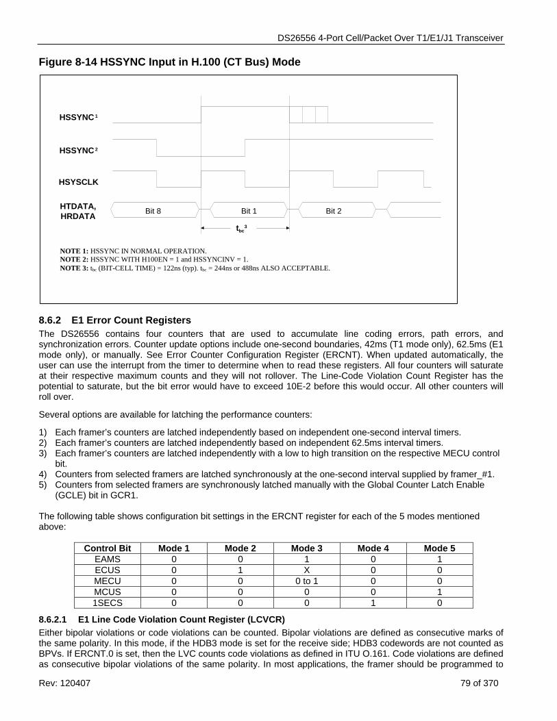
DS26556 4-Port Cell/Packet Over T1/E1/J1 Transceiver
Rev: 120407 79 of 370
Figure 8-14 HSSYNC Input in H.100 (CT Bus) Mode
Bit 8 Bit 1 Bit 2
HSSYNC 1
HSSYNC 2
HSYSCLK
HTDATA,HRDATA
tbc3
NOTE 1: HSSYNC IN NORMAL OPERATION.NOTE 2: HSSYNC WITH H100EN = 1 and HSSYNCINV = 1.NOTE 3: tbc (BIT-CELL TIME) = 122ns (typ). tbc = 244ns or 488ns ALSO ACCEPTABLE.
8.6.2 E1 Error Count Registers The DS26556 contains four counters that are used to accumulate line coding errors, path errors, and synchronization errors. Counter update options include one-second boundaries, 42ms (T1 mode only), 62.5ms (E1 mode only), or manually. See Error Counter Configuration Register (ERCNT). When updated automatically, the user can use the interrupt from the timer to determine when to read these registers. All four counters will saturate at their respective maximum counts and they will not rollover. The Line-Code Violation Count Register has the potential to saturate, but the bit error would have to exceed 10E-2 before this would occur. All other counters will roll over.
Several options are available for latching the performance counters:
1) Each framer’s counters are latched independently based on independent one-second interval timers. 2) Each framer’s counters are latched independently based on independent 62.5ms interval timers. 3) Each framer’s counters are latched independently with a low to high transition on the respective MECU control
bit. 4) Counters from selected framers are latched synchronously at the one-second interval supplied by framer_#1. 5) Counters from selected framers are synchronously latched manually with the Global Counter Latch Enable
(GCLE) bit in GCR1. The following table shows configuration bit settings in the ERCNT register for each of the 5 modes mentioned above:
Control Bit Mode 1 Mode 2 Mode 3 Mode 4 Mode 5 EAMS 0 0 1 0 1 ECUS 0 1 X 0 0 MECU 0 0 0 to 1 0 0 MCUS 0 0 0 0 1 1SECS 0 0 0 1 0
8.6.2.1 E1 Line Code Violation Count Register (LCVCR) Either bipolar violations or code violations can be counted. Bipolar violations are defined as consecutive marks of the same polarity. In this mode, if the HDB3 mode is set for the receive side; HDB3 codewords are not counted as BPVs. If ERCNT.0 is set, then the LVC counts code violations as defined in ITU O.161. Code violations are defined as consecutive bipolar violations of the same polarity. In most applications, the framer should be programmed to
DS26556 4-Port Cell/Packet Over T1/E1/J1 Transceiver
Rev: 120407 80 of 370
count BPVs when receiving AMI code and to count CVs when receiving HDB3 code. This counter increments at all times and is not disabled by loss of sync conditions. The counter saturates at 65,535 and will not rollover. The bit error rate on an E1 line would have to be greater than 10** - 2 before the VCR would saturate. See Table 8-2.
Table 8-2 E1 Line Code Violation Counting Options E1 CODE VIOLATION SELECT
(ERCNT.0) WHAT IS COUNTED IN THE LCVCRs
0 BPVs 1 CVs
8.6.3 DS0 Monitoring Function The DS26556 has the ability to monitor one DS0 64kbps channel in the transmit direction and one DS0 channel in the receive direction at the same time. In the receive direction, the RCM0 to RCM4 bits in the RDS0SEL register need to be properly set and the DS0 channel pointed to by the RCM0 to RCM4 bits will appear in the Receive DS0 (RDS0M) register. The RCM0 to RCM4 bits should be programmed with the decimal decode of the appropriate E1 channel. E1 channels 1 through 32 map to register values 0 through 31. For example, if DS0 channel 15 in the receive direction needed to be monitored, then the following values would be programmed into RDS0SEL:
RCM4 = 0 RCM3 = 1 RCM2 = 1 RCM1 = 1 RCM0 = 0
8.6.4 E1 Receive Signaling Operation Signaling data is sampled in the receive data stream and copied into the receive signaling registers, RS1 through RS16. The signaling information in these registers is always updated on multiframe boundaries. This function is always enabled. NOTE: The receive framer does not normally remove TS16 signaling from the data stream. Signaling information is present in the data stream at the RSER pin unless the receive framer has been programmed to over-lay TS16 with idle codes or to force signaling bit positions to a “one” state. The signaling data in data stream at the HRDATA pin can be re-aligned to a users multiframe reference. See Signaling Reinsertion below. CAS signaling (time slot 16) is sampled in the receive data stream and copied into the receive-signaling registers, RS1 through RS16. The signaling information in these registers is always updated on CAS multiframe boundaries. This function is referred to as “Software Based Signaling” and is always enabled. Time slot 16 is always sampled and loaded into the signaling registers even though CAS signaling data may not be present. When the high speed multiplexed TDM bus is utilized, a TDM signaling stream is available at the HRSIG pin. This is referred to as “Hardware Based Signaling”.
8.6.4.1 Change Of State In order to avoid constantly monitoring of the receive signaling registers the DS26556 can be programmed to alert the host when any specific channel or channels undergo a change of their signaling state. RSCSE1 through RSCSE4 for E1 are used to select which channels can cause a change of state indication. The change of state is indicated in Latched Status Register 4 (RLS4.3). If signaling integration is enabled then the new signaling state must be constant for 3 multiframes before a change of state indication is indicated. The user can enable the INT pin to toggle low upon detection of a change in signaling by setting the appropriate interrupt mask bit RIM4.3. The signaling integration mode is global and cannot be enabled on a channel-by-channel basis.
The user can identity which channels have undergone a signaling change of state by reading the Receive Signaling Status (RSS1 through RSS4) registers. The information from these registers tells the user which RSx register to read for the new signaling data. All changes are indicated in the RSS1–RSS4 registers regardless of the RSCSE1–RSCSE4 registers.
DS26556 4-Port Cell/Packet Over T1/E1/J1 Transceiver
Rev: 120407 81 of 370
8.6.4.2 Hardware-Based Receive Signaling HRSIG is a signaling PCM stream output on a channel-by-channel basis from the signaling buffer. The ABCD signaling bits are output on HRSIG in the lower nibble of each channel. HRSIG is updated once per CAS multiframe (2ms) unless a freeze is in effect. TS16 signaling data is still present in the original data stream at RSER. A signaling buffer provides signaling data to the HRSIG pin and also allows signaling data to be re-inserted into the original data stream in a different alignment that is determined by a multiframe signal from the RSYNC pin. When signaling integration is enabled the signaling data at RSIG is automatically debounced. Signaling must be constant for three multiframes before being up-dated at RSIG. Signaling debounce is enabled on a global basis.
8.6.5 Fractional E1 Support (Gapped Clock Mode) The DS26556 can be programmed to output gapped clocks for selected channels in receive path. When the RCHMRK pin is in the channel clock mode and gapped channel clock is enabled, a gated clock is output on the RCHMRK pin during selected channel times. The channel selection is controlled via the receive-gapped-clock channel-select registers (RGCCS1-RGCCS4). If RCHMRK is in the channel clock mode, clock mode is enabled by the RGCLKEN bit (RESCR.6). Both 56kbps and 64kbps channel formats are supported as determined by RESCR.7. When 56kbps mode is selected, the clock corresponding to the Data/Control bit in the channel is omitted (only the seven most significant bits of the channel have clocks).
8.6.6 Additional Sa-Bit and Si-Bit Receive Operation (E1 Mode) When operated in the E1 mode the DS26556 receiver provides extended access to both the Sa and the Si bits. The RAF and RNAF registers will always report the data as it received in the Sa and Si bit locations. The RAF and RNAF registers are updated on align frame boundaries. The setting of the Receive Align Frame bit in Latched Status Register 2 (RLS2.0) will indicate that the contents of the RAF and RNAF have been updated. The host can use the RLS2.0 bit to know when to read the RAF and RNAF registers. The host has 250μs to retrieve the data before it is lost.
Also there are eight registers (RsiAF, RSiNAF, RRA, Rsa4 to Rsa8) that report the Si and Sa bits as they are received. These registers are updated with the setting of the Receive CRC4 Multiframe bit in Latched Status Register 2 (RLS2.1). The host can use the RLS2.1 bit to know when to read these registers. The user has 2ms to retrieve the data before it is lost. See the register descriptions below for additional information.
8.6.7 HDLC Overhead Control Receive Example The HDLC status registers in the receive framer allow for flexible software interface to meet the user’s preferences. When receiving HDLC messages, the host can chose to be interrupt driven, or to poll to desired status registers, or a combination of polling and interrupt processes may be used. An example routine for using the DS26556 HDLC receiver is given in Figure 8-15.
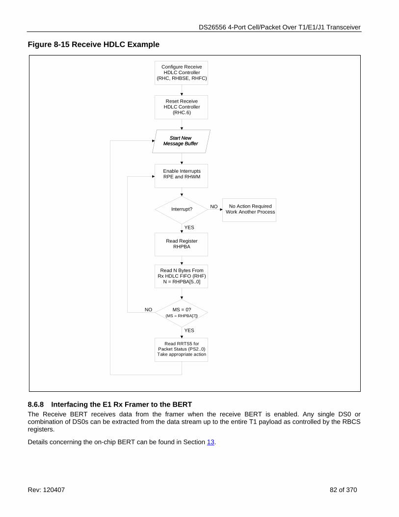
DS26556 4-Port Cell/Packet Over T1/E1/J1 Transceiver
Rev: 120407 82 of 370
Figure 8-15 Receive HDLC Example
Reset Receive HDLC Controller
(RHC.6)
Configure Receive HDLC Controller
(RHC, RHBSE, RHFC)
Start NewMessage Buffer
Enable InterruptsRPE and RHWM
Start NewMessage Buffer
Interrupt?
Read Register RHPBA
Read N Bytes From Rx HDLC FIFO (RHF)
N = RHPBA[5..0]
MS = 0?(MS = RHPBA[7])
NO
YES
NO
YES
Read RRTS5 for Packet Status (PS2..0)Take appropriate action
No Action RequiredWork Another Process
8.6.8 Interfacing the E1 Rx Framer to the BERT The Receive BERT receives data from the framer when the receive BERT is enabled. Any single DS0 or combination of DS0s can be extracted from the data stream up to the entire T1 payload as controlled by the RBCS registers.
Details concerning the on-chip BERT can be found in Section 13.
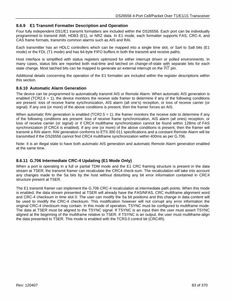
DS26556 4-Port Cell/Packet Over T1/E1/J1 Transceiver
Rev: 120407 83 of 370
8.6.9 E1 Transmit Formatter Description and Operation Four fully independent DS1/E1 transmit formatters are included within the DS26556. Each port can be individually programmed to transmit AMI, HDB3 (E1), or NRZ data. In E1 mode, each formatter supports FAS, CRC-4, and CAS frame formats, transmits common alarms such as AIS and RAI.
Each transmitter has an HDLC controllers which can be mapped into a single time slot, or Sa4 to Sa8 bits (E1 mode) or the FDL (T1 mode) and has 64-byte FIFO buffers in both the transmit and receive paths.
Host interface is simplified with status registers optimized for either interrupt driven or polled environments. In many cases, status bits are reported both real-time and latched on change-of-state with separate bits for each state change. Most latched bits can be mapped to generate an external interrupt on the INT pin.
Additional details concerning the operation of the E1 formatter are included within the register descriptions within this section.
8.6.10 Automatic Alarm Generation The device can be programmed to automatically transmit AIS or Remote Alarm. When automatic AIS generation is enabled (TCR2.6 = 1), the device monitors the receive side framer to determine if any of the following conditions are present: loss of receive frame synchronization, AIS alarm (all one’s) reception, or loss of receive carrier (or signal). If any one (or more) of the above conditions is present, then the framer forces an AIS.
When automatic RAI generation is enabled (TCR2.5 = 1), the framer monitors the receive side to determine if any of the following conditions are present: loss of receive frame synchronization, AIS alarm (all ones) reception, or loss of receive carrier (or signal) or if CRC4 multiframe synchronization cannot be found within 128ms of FAS synchronization (if CRC4 is enabled). If any one (or more) of the above conditions is present, then the framer will transmit a RAI alarm. RAI generation conforms to ETS 300 011 specifications and a constant Remote Alarm will be transmitted if the DS26556 cannot find CRC4 multiframe synchronization within 400ms as per G.706.
Note: It is an illegal state to have both automatic AIS generation and automatic Remote Alarm generation enabled at the same time.
8.6.11 G.706 Intermediate CRC-4 Updating (E1 Mode Only) When a port is operating in a full or partial TDM mode and the E1 CRC framing structure is present in the data stream at TSER, the transmit framer can recalculate the CRC4 check-sum. The recalculation will take into account any changes made to the Sa bits by the host without disturbing any bit error information contained in CRC4 structure present at TSER. The E1 transmit framer can implement the G.706 CRC-4 recalculation at intermediate path points. When this mode is enabled, the data stream presented at TSER will already have the FAS/NFAS, CRC multiframe alignment word and CRC-4 checksum in time slot 0. The user can modify the Sa bit positions and this change in data content will be used to modify the CRC-4 checksum. This modification however will not corrupt any error information the original CRC-4 checksum may contain. In this mode of operation, TSYNC must be configured to multiframe mode. The data at TSER must be aligned to the TSYNC signal. If TSYNC is an input then the user must assert TSYNC aligned at the beginning of the multiframe relative to TSER. If TSYNC is an output, the user must multiframe-align the data presented to TSER. This mode is enabled with the TCR3.0 control bit (CRC4R).
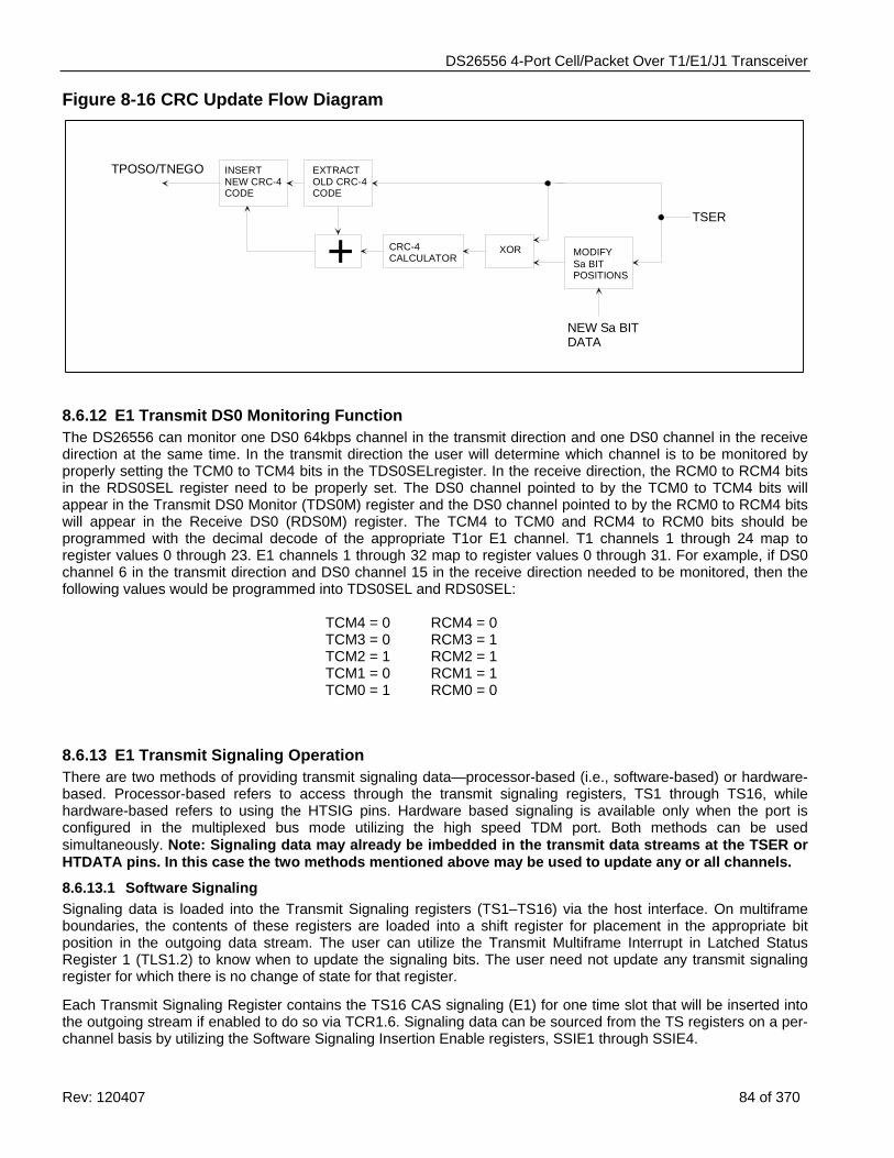
DS26556 4-Port Cell/Packet Over T1/E1/J1 Transceiver
Rev: 120407 84 of 370
Figure 8-16 CRC Update Flow Diagram
TSER
XORCRC-4CALCULATOR
EXTRACTOLD CRC-4CODE
INSERTNEW CRC-4CODE
MODIFYSa BITPOSITIONS
NEW Sa BITDATA
+
TPOSO/TNEGO
8.6.12 E1 Transmit DS0 Monitoring Function The DS26556 can monitor one DS0 64kbps channel in the transmit direction and one DS0 channel in the receive direction at the same time. In the transmit direction the user will determine which channel is to be monitored by properly setting the TCM0 to TCM4 bits in the TDS0SELregister. In the receive direction, the RCM0 to RCM4 bits in the RDS0SEL register need to be properly set. The DS0 channel pointed to by the TCM0 to TCM4 bits will appear in the Transmit DS0 Monitor (TDS0M) register and the DS0 channel pointed to by the RCM0 to RCM4 bits will appear in the Receive DS0 (RDS0M) register. The TCM4 to TCM0 and RCM4 to RCM0 bits should be programmed with the decimal decode of the appropriate T1or E1 channel. T1 channels 1 through 24 map to register values 0 through 23. E1 channels 1 through 32 map to register values 0 through 31. For example, if DS0 channel 6 in the transmit direction and DS0 channel 15 in the receive direction needed to be monitored, then the following values would be programmed into TDS0SEL and RDS0SEL:
TCM4 = 0 RCM4 = 0 TCM3 = 0 RCM3 = 1 TCM2 = 1 RCM2 = 1 TCM1 = 0 RCM1 = 1 TCM0 = 1 RCM0 = 0
8.6.13 E1 Transmit Signaling Operation There are two methods of providing transmit signaling data—processor-based (i.e., software-based) or hardware-based. Processor-based refers to access through the transmit signaling registers, TS1 through TS16, while hardware-based refers to using the HTSIG pins. Hardware based signaling is available only when the port is configured in the multiplexed bus mode utilizing the high speed TDM port. Both methods can be used simultaneously. Note: Signaling data may already be imbedded in the transmit data streams at the TSER or HTDATA pins. In this case the two methods mentioned above may be used to update any or all channels.
8.6.13.1 Software Signaling Signaling data is loaded into the Transmit Signaling registers (TS1–TS16) via the host interface. On multiframe boundaries, the contents of these registers are loaded into a shift register for placement in the appropriate bit position in the outgoing data stream. The user can utilize the Transmit Multiframe Interrupt in Latched Status Register 1 (TLS1.2) to know when to update the signaling bits. The user need not update any transmit signaling register for which there is no change of state for that register.
Each Transmit Signaling Register contains the TS16 CAS signaling (E1) for one time slot that will be inserted into the outgoing stream if enabled to do so via TCR1.6. Signaling data can be sourced from the TS registers on a per-channel basis by utilizing the Software Signaling Insertion Enable registers, SSIE1 through SSIE4.
DS26556 4-Port Cell/Packet Over T1/E1/J1 Transceiver
Rev: 120407 85 of 370
TS16 carries the signaling information. This information can be in either CCS (Common Channel Signaling) or CAS (Channel Associated Signaling) format. The 32 time slots are referenced by two different channel number schemes in E1. In “Channel” numbering, TS0 through TS31 are labeled channels 1 through 32. In “Phone Channel” numbering TS1 through TS15 are labeled channel 1 through channel 15 and TS17 through TS31 are labeled channel 15 through channel 30.
8.6.13.2 Hardware Signaling Hardware signaling is only available when the port is configured to use the high speed TDM bus. Note: the cell/packet interface is unavailable to this port in this mode. In hardware mode, signaling data is input via the HTSIG pin. This signaling PCM stream is demultiplexed, buffered and inserted to the data stream input from the demultiplexed HTDATA pin.
The user has the ability to control which channels are to have signaling data from the HTSIG pin inserted into them on a per-channel basis via the THSCS1 through THSCS4 registers.
Figure 8-17 Time Slot Numbering Schemes TS 0 1 2 3 4 5 6 7 8 9 10 11 12 13 14 15 16 17 18 19 20 21 22 23 24 25 26 27 28 29 30 31
Channel 1 2 3 4 5 6 7 8 9 10 11 12 13 14 15 16 17 18 19 20 21 22 23 24 25 26 27 28 29 30 31 32Phone
Channel 1 2 3 4 5 6 7 8 9 10 11 12 13 14 15 16 17 18 19 20 21 22 23 24 25 26 27 28 29 30
8.6.14 Fractional E1 Support (Gapped Clock Mode) The DS26556 can be programmed to output gapped clocks for selected channels in transmit path. When the TCHMRK pin is in the channel clock mode and gapped channel clock is enabled, a gated clock is output on the TCHMRK pin during selected channel times. The channel selection is controlled via the transmit-gapped-clock channel-select registers (TGCCS1-TGCCS4). If TCHMRK is in the channel clock mode clock mode is enabled by the TGCLKEN bit (TESCR.6). Both 56kbps and 64kbps channel formats are supported as determined by TESCR.7. When 56kbps mode is selected, the clock corresponding to the Data/Control bit in the channel is omitted (only the seven most significant bits of the channel have clocks).
8.6.15 Additional (Sa) and International (Si) Bit Operation (E1 Mode) On the transmit side, data is sampled from the TAF and TNAF registers with the setting of the Transmit Align Frame bit in Transmit Status Register 1 (TLS1.3). The host can use the TLS1.3 bit to know when to update the TAF and TNAF registers. It has 250μs to update the data or else the old data will be retransmitted. NOTE: If the TAF an TNAF registers are only being used to source the align frame and non-align frame sync patterns then the host need only write once to these registers. Data in the Si bit position will be overwritten if either the framer is programmed: (1) to source the Si bits from the TSER pin, (2) in the CRC4 mode, or (3) have automatic E-bit insertion enabled.
There is also a set of eight registers (TSiAF, TSiNAF, TRA, TSa4 to TSa8) that, via the Transmit Sa-Bit Control Register (TSaCR), can be programmed to insert both Si and Sa data. Data is sampled from these registers with the setting of the Transmit Multiframe bit in Status Register 1 (TLS1.3). The host can use the TLS1.3 bit to know when to update these registers. It has 2ms to update the data or else the old data will be retransmitted.
8.6.16 E1 Transmit HDLC Controller Each framer port has an HDLC controller with 64-byte FIFOs. The HDLC controller can be mapped into a single time slot, or Sa4 to Sa8 bits (E1 Mode) or the FDL (T1 mode). This block has 64-byte FIFO buffers in both the transmit and receive paths. The user can select any specific bits within the time slot(s) to assign to the HDLC controller, as well as specific Sa bits (E1 mode). The HDLC controllers automatically generate and detect flags, generate and check the CRC checksum, generate and detect abort sequences, stuff and destuff zeros, and byte align to the data stream.
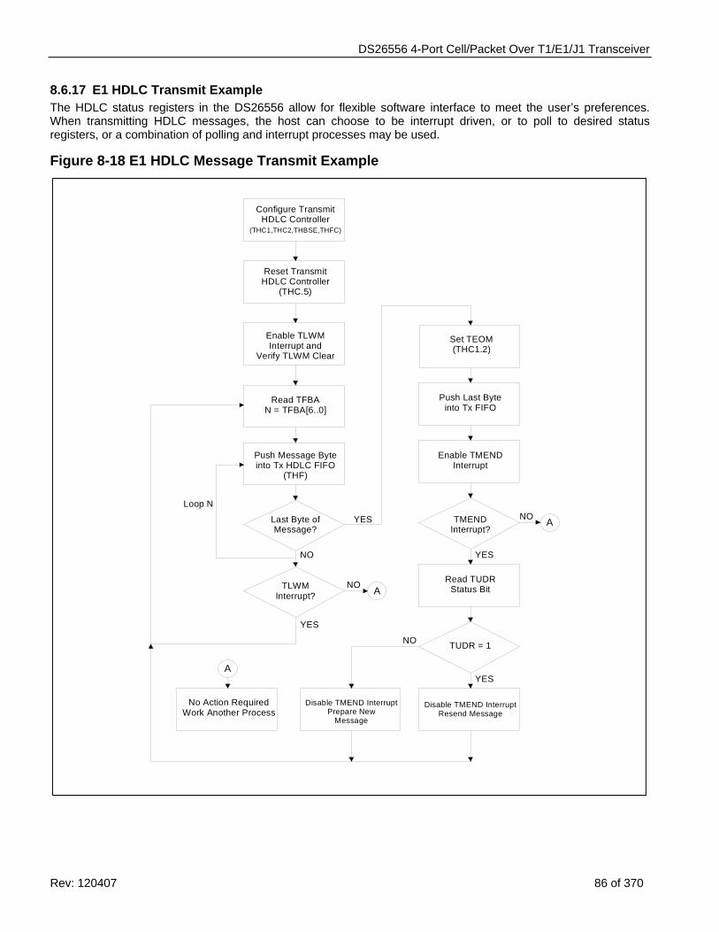
DS26556 4-Port Cell/Packet Over T1/E1/J1 Transceiver
Rev: 120407 86 of 370
8.6.17 E1 HDLC Transmit Example The HDLC status registers in the DS26556 allow for flexible software interface to meet the user’s preferences. When transmitting HDLC messages, the host can choose to be interrupt driven, or to poll to desired status registers, or a combination of polling and interrupt processes may be used.
Figure 8-18 E1 HDLC Message Transmit Example
Reset Transmit HDLC Controller
(THC.5)
Configure Transmit HDLC Controller
(THC1,THC2,THBSE,THFC)
TLWM Interrupt?
Enable TMENDInterrupt
No Action RequiredWork Another Process
Enable TLWM Interrupt and
Verify TLWM Clear
Read TFBAN = TFBA[6..0]
Push Message Byteinto Tx HDLC FIFO
(THF)
Last Byte ofMessage?
YES
NO
Set TEOM (THC1.2)
Push Last Byteinto Tx FIFO
Loop N
TMENDInterrupt?
YES
Read TUDR Status Bit
TUDR = 1
YES
Disable TMEND InterruptResend Message
Disable TMEND InterruptPrepare New
Message
YES
NO
NO
NO
A
A
A
DS26556 4-Port Cell/Packet Over T1/E1/J1 Transceiver
Rev: 120407 87 of 370
8.6.18 Interfacing the E1 Transmitter to the BERT If the Transmit BERT is enabled, data will be inserted from the BERT into the transmit formatter. Any single DS0 or combination of DS0s can be inserted into the data stream up to the entire T1 payload as controlled by the RBCS registers.
Details concerning the BERT can be found in Section 13.
8.6.19 E1 Transmit Synchronizer The DS26556 transmitter can identify the E1 frame boundary, as well as the CRC multiframe boundaries within the incoming NRZ data stream at TSER. Control signals for the transmit synchronizer are located in the TSYNCC register. The Transmit Synchronizer Status (TSYNCS) register provides a latched status bit (LOFD) to indicate that a loss-of-frame synchronization has occurred, and a real-time bit (LOF) which is set high when the synchronizer is searching for frame/multiframe alignment. The LOFD bit can be enabled to cause an interrupt condition on INT.
Note that when the transmit synchronizer is used, the TSYNC signal should be set as an output (TSIO = 1) and the recovered frame sync pulse will be output on this signal. The recovered CRC4 multiframe sync pulse will be output if enabled with TIOCR.0 (TSM = 1).
DS26556 4-Port Cell/Packet Over T1/E1/J1 Transceiver
Rev: 120407 88 of 370
9 LINE INTERFACE UNIT (LIU) The DS26556’s LIU provides the necessary transmit pulse shaping and receive signal processing for long-haul, short-haul, FCC CSU build-outs, and clock-synchronization applications. The transmitter and receiver have software selectable, internal termination for 75Ω, 100Ω, 110Ω, and 120Ω networks. The LIU block also contains a jitter attenuator that can be assigned to either the transmit or receive path, or disabled. Several loopbacks are provided for network and system side diagnostics. Each port’s LIU can be configured independently. The table below describes the registers involved in control and configuration of the LIUs.
9.1 LIU Transmitter
9.1.1 Pulse Shapes
The transmit pulse shape is configured on a port-by-port basis. Pulse shapes are typically measured and compared to the appropriate pulse template at two locations in the network. For T1 long haul and FCC CSU applications the pulse is measured at the near-end NI (Network Interface). For T1 short haul applications the pulse is measured at the far-end NI. All E1 pulse shapes are measured at the near-end NI.
9.1.2 Transmit Termination
The LIU Transmit Impedance Selection Registers can be used to select an internal Transmit Terminating Impedance of 100Ω for T1, 110Ω for J1 Mode, 75Ω or 120Ω for E1 Mode, or no internal Termination for E1 or T1 Mode. In this case the user has to provide the Line Terminating Network. The transmit pulse shape and terminating impedance is selected by the LTCR register.
9.1.3 Power-Down and High-Z
The DS26556 provides the ability to individually power-down the transmitters and/or place the transmit drivers into a High-Z state via register bits or device pins. This is useful for Protection Switching applications.
The transmitters can be powered down by setting the TPDE bit in the LCCR2 register. Note that powering down the transmit LIU results in a High-Z state for the corresponding TTIP and TRING pins.
9.1.4 Transmit All Ones
When Transmit All Ones is invoked in the LIU block, continuous ones are transmitted using MCLK as the timing reference. Data and clock from the framer is ignored. Transmit all ones can be sent by setting a bit in the LCCR2 register. Also transmit all ones will be are sent if the corresponding receiver goes into LOS state and the ATOS bit is set in the LCCR2 register.
9.1.5 Driver Fail Monitor
The transmit drivers have a monitor that will detect short circuit and open-circuit conditions at the TTIP and TRING pins. The drive current will be limited if a short circuit is detected. The status registers can be used to alert the user to an open circuit or short circuit condition.
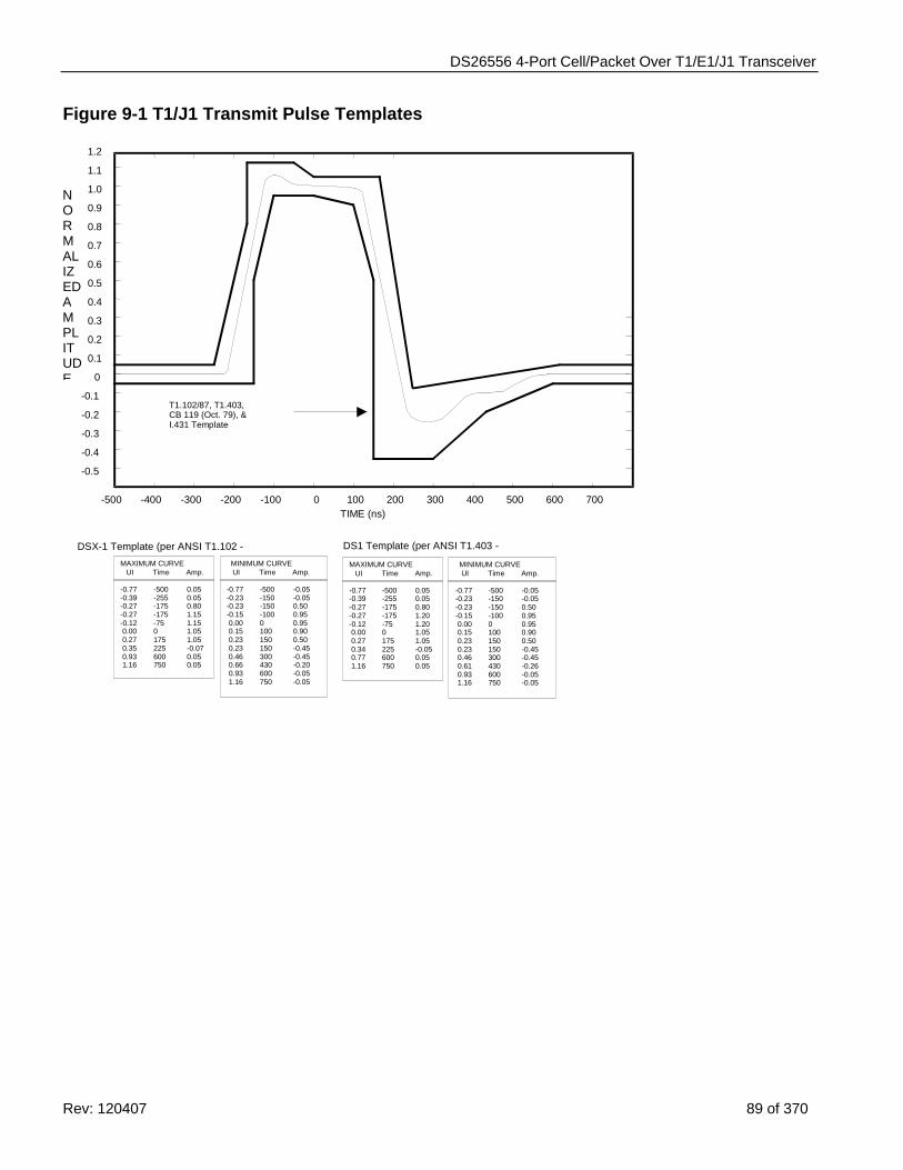
DS26556 4-Port Cell/Packet Over T1/E1/J1 Transceiver
Rev: 120407 89 of 370
Figure 9-1 T1/J1 Transmit Pulse Templates
1.2
0 -0.1 -0.2 -0.3 -0.4 -0.5
0.1 0.2 0.3 0.4 0.5 0.6 0.7 0.8 0.9 1.0 1.1
-500 -300 -100 0 300 500 700-400 -200 200 400 600100TIME (ns)
NORMALIZED AMPLITUDE
T1.102/87, T1.403, CB 119 (Oct. 79), & I.431 Template
-0.77 -0.39 -0.27 -0.27 -0.12 0.00 0.27 0.35 0.93 1.16
-500 -255 -175 -175 -75 0 175 225 600 750
0.05 0.05 0.80 1.15 1.15 1.05 1.05 -0.07 0.05 0.05
-0.77 -0.23 -0.23 -0.15 0.00 0.15 0.23 0.23 0.46 0.66 0.93 1.16
-500 -150 -150 -100 0 100150150300430600750
-0.05 -0.05 0.50 0.95 0.95 0.90 0.50 -0.45 -0.45 -0.20 -0.05 -0.05
UI Time Amp. MAXIMUM CURVE UI Time Amp. MINIMUM CURVE
-0.77-0.39-0.27-0.27-0.12 0.00 0.27 0.34 0.77 1.16
-500-255-175-175-750175225600750
0.050.050.801.201.201.051.05-0.050.050.05
-0.77-0.23-0.23-0.15 0.00 0.15 0.23 0.23 0.46 0.61 0.93 1.16
-500-150-150-1000100150150300430600750
-0.05-0.050.500.950.950.900.50-0.45-0.45-0.26-0.05-0.05
UI Time Amp.MAXIMUM CURVE
UI Time Amp.MINIMUM CURVE
DSX-1 Template (per ANSI T1.102 -1993)
DS1 Template (per ANSI T1.403 -1995)
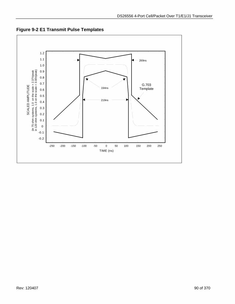
DS26556 4-Port Cell/Packet Over T1/E1/J1 Transceiver
Rev: 120407 90 of 370
Figure 9-2 E1 Transmit Pulse Templates
0
-0.1
-0.2
0.1
0.2
0.3
0.4
0.5
0.6
0.7
0.8
0.9
1.0
1.1
1.2
0
TIME (ns)
SC
ALE
D A
MP
LITU
DE
50 100 150 200 250-50-100-150-200-250
269ns
194ns
219ns
(in 7
5 oh
m s
yste
ms,
1.0
on
the
scal
e =
2.37
Vpe
ak in
120
ohm
sys
tem
s, 1
.0 o
n th
e sc
ale
= 3.
00V
peak
)
G.703Template
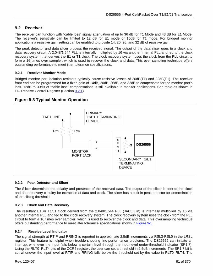
DS26556 4-Port Cell/Packet Over T1/E1/J1 Transceiver
Rev: 120407 91 of 370
9.2 Receiver The receiver can function with “cable loss” signal attenuation of up to 36 dB for T1 Mode and 43 dB for E1 Mode. The receiver’s sensitivity can be limited to 12 dB for E1 mode or 15dB for T1 mode. For bridged monitor applications a resistive gain setting can be enabled to provide 14, 20, 26, and 32 dB of resistive gain.
The peak detector and data slicer process the received signal. The output of the data slicer goes to a clock and data recovery circuit. A 2.048/1.544 PLL is internally multiplied by 16 via another internal PLL and fed to the clock recovery system that derives the E1 or T1 clock. The clock recovery system uses the clock from the PLL circuit to form a 16 times over sampler, which is used to recover the clock and data. This over sampling technique offers outstanding performance to meet jitter tolerance specifications.
9.2.1 Receiver Monitor Mode
Bridged monitor port isolation resistors typically cause resistive losses of 20dB(T1) and 32dB(E1). The receiver front end can be programmed for a fixed gain of 14dB, 20dB, 26dB, and 32dB to compensate for the monitor port’s loss. 12dB to 30dB of “cable loss” compensations is still available in monitor applications. See table as shown in LIU Receive Control Register (Section 9.2.1).
Figure 9-3 Typical Monitor Operation
9.2.2 Peak Detector and Slicer
The Slicer determines the polarity and presence of the received data. The output of the slicer is sent to the clock and data recovery circuitry for extraction of data and clock. The slicer has a built-in peak detector for determination of the slicing threshold.
9.2.3 Clock and Data Recovery
The resultant E1 or T1/J1 clock derived from the 2.048/1.544 PLL (JACLK in) is internally multiplied by 16 via another internal PLL and fed to the clock recovery system. The clock recovery system uses the clock from the PLL circuit to form a 16 times over sampler, which is used to recover the clock and data. This oversampling technique offers outstanding performance to meet jitter tolerance specifications shown in Figure 9-5.
9.2.4 Receive Level Indicator The signal strength at RTIP and RRING is reported in approximate 2.5dB increments via RSL3-RSL0 in the LRSL register. This feature is helpful when trouble-shooting line-performance problems. The DS26556 can initiate an interrupt whenever the input falls below a certain level through the input-level under-threshold indicator (SR1.7). Using the RLT0–RLT4 bits of the CCR4 register, the user can set a threshold in 2.5dB increments. The SR1.7 bit is set whenever the input level at RTIP and RRING falls below the threshold set by the value in RLT0–RLT4. The
PRIMARYT1/E1 TERMINATINGDEVICE
MONITORPORT JACK
T1/E1 LINE
XFMR
DS26556Rt
Rm Rm
SECONDARY T1/E1TERMINATINGDEVICE
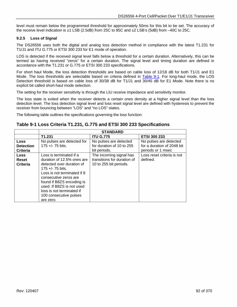
DS26556 4-Port Cell/Packet Over T1/E1/J1 Transceiver
Rev: 120407 92 of 370
level must remain below the programmed threshold for approximately 50ms for this bit to be set. The accuracy of the receive level indication is ±1 LSB (2.5dB) from 25C to 85C and ±2 LSB’s (5dB) from –40C to 25C.
9.2.5 Loss of Signal
The DS26556 uses both the digital and analog loss detection method in compliance with the latest T1.231 for T1/J1 and ITU G.775 or ETSI 300 233 for E1 mode of operation.
LOS is detected if the received signal level falls below a threshold for a certain duration. Alternatively, this can be termed as having received “zeros” for a certain duration. The signal level and timing duration are defined in accordance with the T1.231 or G.775 or ETSI 300 233 specifications.
For short haul Mode, the loss detection thresholds are based on cable loss of 12/18 dB for both T1/J1 and E1 Mode. The loss thresholds are selectable based on criteria defined in Table 9-1. For long-haul mode, the LOS Detection threshold is based on cable loss of 30/38 dB for T1/J1 and 30/45 dB for E1 Mode. Note there is no explicit bit called short-haul mode selection.
The setting for the receiver sensitivity is through the LIU receive impedance and sensitivity monitor.
The loss state is exited when the receiver detects a certain ones density at a higher signal level than the loss detection level. The loss detection signal level and loss reset signal level are defined with hysteresis to prevent the receiver from bouncing between “LOS” and “no LOS” states.
The following table outlines the specifications governing the loss function:
Table 9-1 Loss Criteria T1.231, G.775 and ETSI 300 233 Specifications STANDARD T1.231 ITU G.775 ETSI 300 233 Loss Detection Criteria
No pulses are detected for 175 +/- 75 bits.
No pulses are detected for duration of 10 to 255 bit periods.
No pulses are detected for a duration of 2048 bit periods or 1 msec
Loss Reset Criteria
Loss is terminated if a duration of 12.5% ones are detected over duration of 175 +/- 75 bits. Loss is not terminated if 8 consecutive zeros are found if B8ZS encoding is used. If B8ZS is not used loss is not terminated if 100 consecutive pulses are zero.
The incoming signal has transitions for duration of 10 to 255 bit periods.
Loss reset criteria is not defined.
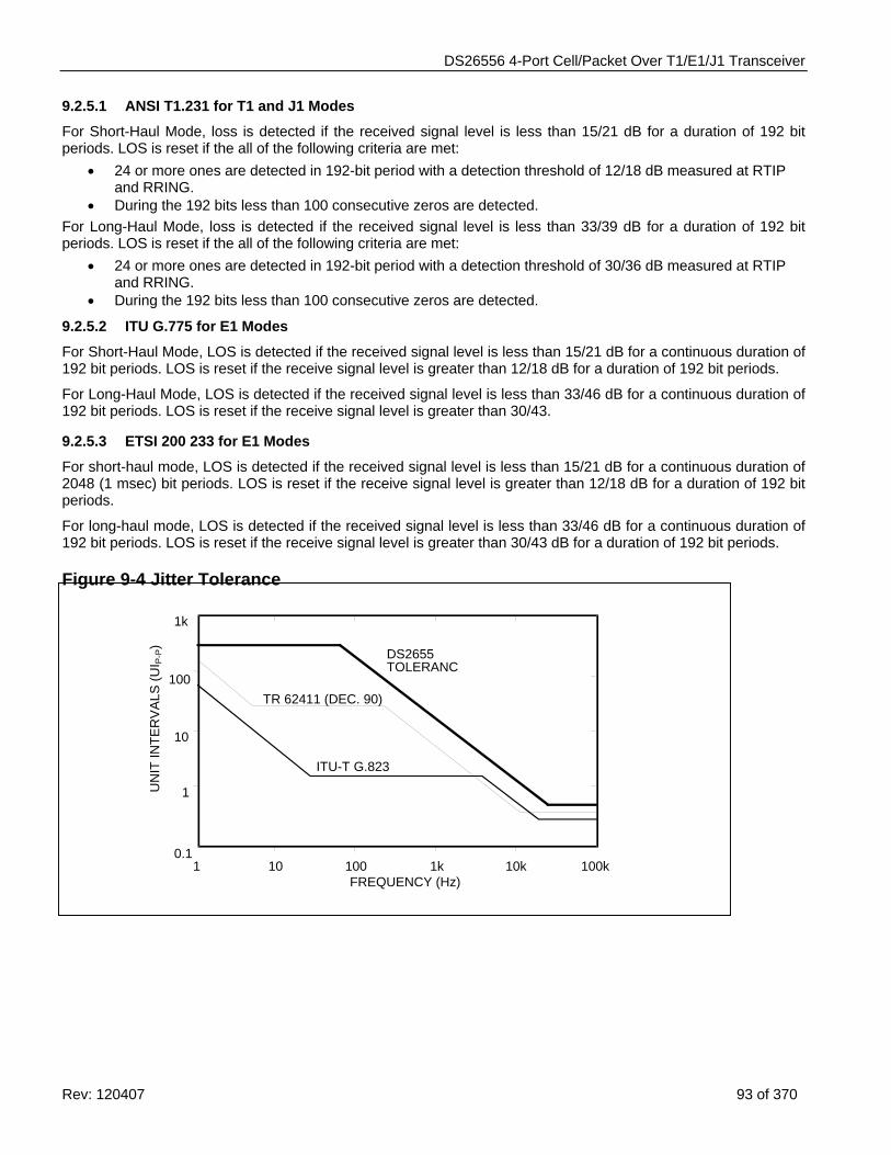
DS26556 4-Port Cell/Packet Over T1/E1/J1 Transceiver
Rev: 120407 93 of 370
FREQUENCY (Hz)
UN
IT IN
TER
VA
LS (U
I P-P
)
1k
100
10
1
0.1 10 100 1k 10k 100k
DS2655TOLERANC
1
TR 62411 (DEC. 90)
ITU-T G.823
9.2.5.1 ANSI T1.231 for T1 and J1 Modes
For Short-Haul Mode, loss is detected if the received signal level is less than 15/21 dB for a duration of 192 bit periods. LOS is reset if the all of the following criteria are met:
• 24 or more ones are detected in 192-bit period with a detection threshold of 12/18 dB measured at RTIP and RRING.
• During the 192 bits less than 100 consecutive zeros are detected. For Long-Haul Mode, loss is detected if the received signal level is less than 33/39 dB for a duration of 192 bit periods. LOS is reset if the all of the following criteria are met:
• 24 or more ones are detected in 192-bit period with a detection threshold of 30/36 dB measured at RTIP and RRING.
• During the 192 bits less than 100 consecutive zeros are detected.
9.2.5.2 ITU G.775 for E1 Modes
For Short-Haul Mode, LOS is detected if the received signal level is less than 15/21 dB for a continuous duration of 192 bit periods. LOS is reset if the receive signal level is greater than 12/18 dB for a duration of 192 bit periods.
For Long-Haul Mode, LOS is detected if the received signal level is less than 33/46 dB for a continuous duration of 192 bit periods. LOS is reset if the receive signal level is greater than 30/43.
9.2.5.3 ETSI 200 233 for E1 Modes
For short-haul mode, LOS is detected if the received signal level is less than 15/21 dB for a continuous duration of 2048 (1 msec) bit periods. LOS is reset if the receive signal level is greater than 12/18 dB for a duration of 192 bit periods.
For long-haul mode, LOS is detected if the received signal level is less than 33/46 dB for a continuous duration of 192 bit periods. LOS is reset if the receive signal level is greater than 30/43 dB for a duration of 192 bit periods.
Figure 9-4 Jitter Tolerance
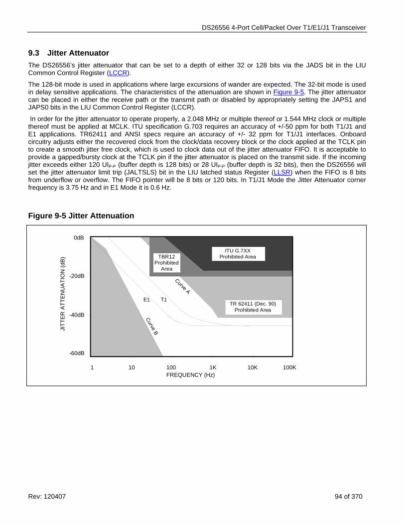
DS26556 4-Port Cell/Packet Over T1/E1/J1 Transceiver
Rev: 120407 94 of 370
9.3 Jitter Attenuator The DS26556’s jitter attenuator that can be set to a depth of either 32 or 128 bits via the JADS bit in the LIU Common Control Register (LCCR).
The 128-bit mode is used in applications where large excursions of wander are expected. The 32-bit mode is used in delay sensitive applications. The characteristics of the attenuation are shown in Figure 9-5. The jitter attenuator can be placed in either the receive path or the transmit path or disabled by appropriately setting the JAPS1 and JAPS0 bits in the LIU Common Control Register (LCCR).
In order for the jitter attenuator to operate properly, a 2.048 MHz or multiple thereof or 1.544 MHz clock or multiple thereof must be applied at MCLK. ITU specification G.703 requires an accuracy of +/-50 ppm for both T1/J1 and E1 applications. TR62411 and ANSI specs require an accuracy of +/- 32 ppm for T1/J1 interfaces. Onboard circuitry adjusts either the recovered clock from the clock/data recovery block or the clock applied at the TCLK pin to create a smooth jitter free clock, which is used to clock data out of the jitter attenuator FIFO. It is acceptable to provide a gapped/bursty clock at the TCLK pin if the jitter attenuator is placed on the transmit side. If the incoming jitter exceeds either 120 UIP-P (buffer depth is 128 bits) or 28 UIP-P (buffer depth is 32 bits), then the DS26556 will set the jitter attenuator limit trip (JALTSLS) bit in the LIU latched status Register (LLSR) when the FIFO is 8 bits from underflow or overflow. The FIFO pointer will be 8 bits or 120 bits. In T1/J1 Mode the Jitter Attenuator corner frequency is 3.75 Hz and in E1 Mode it is 0.6 Hz.
Figure 9-5 Jitter Attenuation
FREQUENCY (Hz)
0dB
-20dB
-40dB
-60dB
1 10 100 1K 10K
JITT
ER
ATT
EN
UA
TIO
N (d
B)
100K
TR 62411 (Dec. 90)Prohibited Area
Curve B
Curve A
ITU G.7XXProhibited AreaTBR12
ProhibitedArea
T1E1
DS26556 4-Port Cell/Packet Over T1/E1/J1 Transceiver
Rev: 120407 95 of 370
9.4 LIU Loopbacks The DS26556 provides three loopbacks in the LIU block: analog loopback (ALB), local loopback (LLB), and remote loopback (RLB). Remote loopback (RLB) and local loopback (LLB) may be enabled simultaneously. Additionally, the framer block provides framer loopback (FLB) discussed in the framer section of the datasheet.
9.4.1 Analog Loopback TTIP and TRING are looped to RTIP and RRING. Externally, signals at RTIP and RRING are ignored.
9.4.2 Local Loopback Data from the transmit backplane interface is looped back to the receive backplane interface. Data form the transmit system backplane will continue to be transmitted as normal.
9.4.3 Remote Loopback The inputs decoded from the Receive LIU are looped back to the Transmit LIU. The inputs from the Transmit Framer are ignored during a remote loopback.
DS26556 4-Port Cell/Packet Over T1/E1/J1 Transceiver
Rev: 120407 96 of 370
10 OVERALL REGISTER MAP
Table 10-1 Overall Register Map
Address Description
0000 – 01FF Port 1 Framer
0200 – 03FF Port 2 Framer
0400 – 05FF Port 3 Framer
0600 – 07FF Port 4 Framer
0800 – 09FF Port 1 LIU
0A00 – 0BFF Port 2 LIU
0C00 – 0DFF Port 3 LIU
0E00 – 0FFF Port 4 LIU
1000 – 11FF Port 1 Cell/Packet Processor
1200 – 13FF Port 2 Cell/Packet Processor
1400 – 15FF Port 3 Cell/Packet Processor
1600 – 17FF Port 4 Cell/Packet Processor
1800 – 18FF Global Registers
1900 – 19FF System Interface Registers
1A00 - 1FFF Unused
The address offset for each port:
Port 1 – No Offset
Port 2 – Port 1 Address + 0200 Hex
Port 3 – Port 1 Address + 0400 Hex
Port 4 – Port 1 Address + 0600 Hex
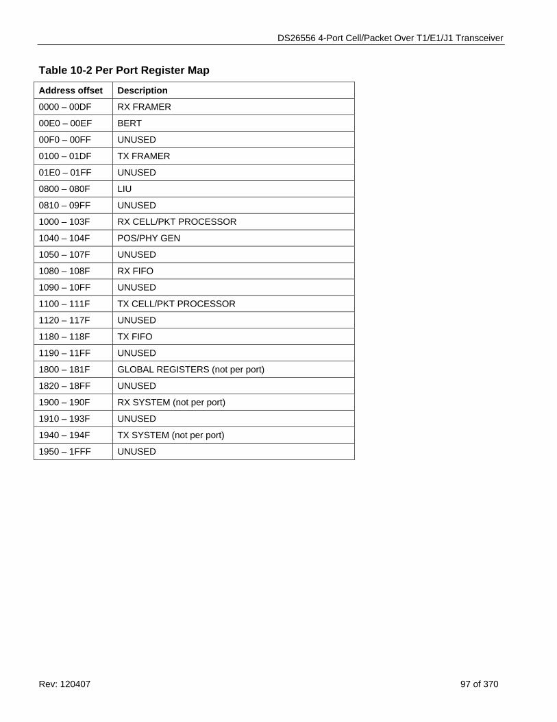
DS26556 4-Port Cell/Packet Over T1/E1/J1 Transceiver
Rev: 120407 97 of 370
Table 10-2 Per Port Register Map
Address offset Description
0000 – 00DF RX FRAMER
00E0 – 00EF BERT
00F0 – 00FF UNUSED
0100 – 01DF TX FRAMER
01E0 – 01FF UNUSED
0800 – 080F LIU
0810 – 09FF UNUSED
1000 – 103F RX CELL/PKT PROCESSOR
1040 – 104F POS/PHY GEN
1050 – 107F UNUSED
1080 – 108F RX FIFO
1090 – 10FF UNUSED
1100 – 111F TX CELL/PKT PROCESSOR
1120 – 117F UNUSED
1180 – 118F TX FIFO
1190 – 11FF UNUSED
1800 – 181F GLOBAL REGISTERS (not per port)
1820 – 18FF UNUSED
1900 – 190F RX SYSTEM (not per port)
1910 – 193F UNUSED
1940 – 194F TX SYSTEM (not per port)
1950 – 1FFF UNUSED
DS26556 4-Port Cell/Packet Over T1/E1/J1 Transceiver
Rev: 120407 98 of 370
11 REGISTER MAPS AND DESCRIPTIONS
11.1 Global Registers
Table 11-1 Global Register Map
ADDRESS NAME FUNCTION 1800 IDR Device ID Register 1801 GCR1 Global Control Register 1 1802 GCR2 Global Control Register 2 1803 GCR3 Global Control Register 3 1804 GCR4 Global Control Register 4 1805 GCR5 Global Control Register 5 1806 GCCR Global Clock Control Register 1807 GSRR Global Software Reset Register 1808 GRTPFS Global RCHMRK and TCHMRK Pin Function Select Register 1809 GSR1 Global Status Register 1 180A GSR2 Global Status Register 2 180B GSR3 Global Status Register 3 180C GSR4 Global Status Register 4 180D GSRL4 Global Status Register Latched 4 180E GIM1 Global Interrupt Mask Register 1 180F GIM2 Global Interrupt Mask Register 2 1810 GIM3 Global Interrupt Mask Register 3 1811 GIM4 Global Interrupt Mask Register Latched 4
1812 – 18FF — Unused. Must be set = 0 for proper operation.
11.1.1 Global Control Registers Register Name: IDR Register Description: Device Identification Register Address (hex): 1800 Bit # 7 6 5 4 3 2 1 0 Name ID7 ID6 ID5 ID4 ID3 ID2 ID1 ID0 Default 0 0 0 0 0 0 0 0 Bits 7 to 4 : Device ID (ID7 to ID4) The upper four bits of the IDR are used to display the DS26556 ID. Bits 3 to 0 : Chip Revision Bits (ID3 to ID0) The lower four bits of the IDR are used to display the die revision of the chip. IDO is the LSB of a decimal code that represents the chip revision. DEVICE ID (ID7 to ID4) DS26556 0000
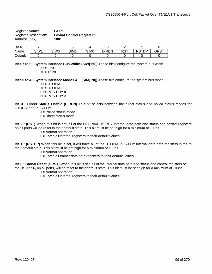
DS26556 4-Port Cell/Packet Over T1/E1/J1 Transceiver
Rev: 120407 99 of 370
Register Name: GCR1 Register Description: Global Control Register 1 Address (hex): 1801 Bit # 7 6 5 4 3 2 1 0 Name SIW1 SIW0 SIM1 SIM0 DIREN RST RSTDP GRST Default 0 0 0 0 0 0 0 0 Bits 7 to 6 : System Interface Bus Width (SIW[1:0]) These bits configure the system bus width. 00 = 8 bit 01 = 16 bit Bits 5 to 4 : System Interface Mode1 & 0 (SIM[1:0]) These bits configure the system bus mode. 00 = UTOPIA II 01 = UTOPIA 3 10 = POS-PHY II 11 = POS-PHY 3 Bit 3 : Direct Status Enable (DIREN) This bit selects between the direct status and polled status modes for UTOPIA and POS-PHY. 0 = Polled status mode 1 = Direct status mode Bit 2 : (RST) When this bit is set, all of the UTOPIA/POS-PHY internal data path and status and control registers on all ports will be reset to their default state. This bit must be set high for a minimum of 100ns. 0 = Normal operation. 1 = Force all internal registers to their default values Bit 1 : (RSTDP) When this bit is set, it will force all of the UTOPIA/POS-PHY internal data path registers in the to their default state. This bit must be set high for a minimum of 100ns. 0 = Normal operation. 1 = Force all framer data path registers to their default values. Bit 0 : Global Reset (GRST) When this bit is set, all of the internal data path and status and control registers of the DS26556, on all ports, will be reset to their default state. This bit must be set high for a minimum of 100ns. 0 = Normal operation. 1 = Force all internal registers to their default values.
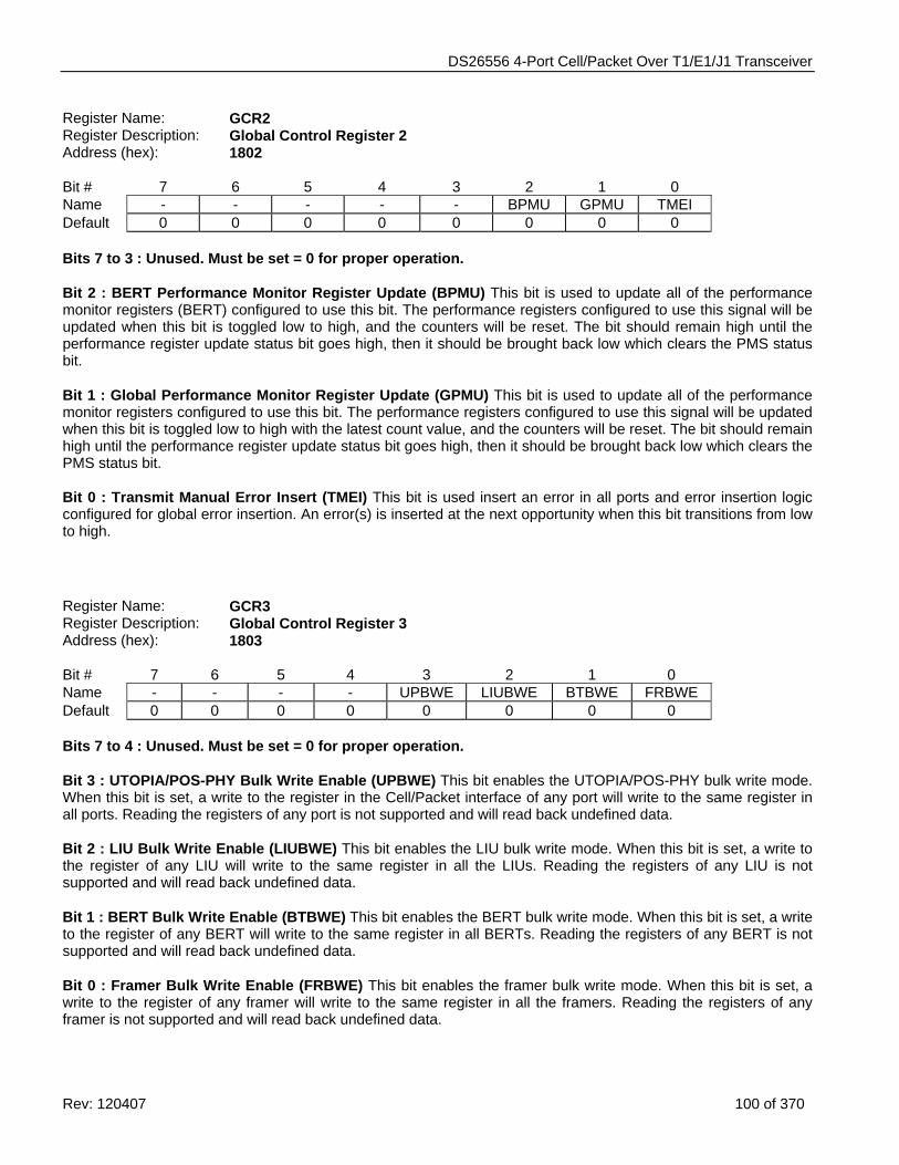
DS26556 4-Port Cell/Packet Over T1/E1/J1 Transceiver
Rev: 120407 100 of 370
Register Name: GCR2 Register Description: Global Control Register 2 Address (hex): 1802 Bit # 7 6 5 4 3 2 1 0 Name - - - - - BPMU GPMU TMEI Default 0 0 0 0 0 0 0 0 Bits 7 to 3 : Unused. Must be set = 0 for proper operation. Bit 2 : BERT Performance Monitor Register Update (BPMU) This bit is used to update all of the performance monitor registers (BERT) configured to use this bit. The performance registers configured to use this signal will be updated when this bit is toggled low to high, and the counters will be reset. The bit should remain high until the performance register update status bit goes high, then it should be brought back low which clears the PMS status bit. Bit 1 : Global Performance Monitor Register Update (GPMU) This bit is used to update all of the performance monitor registers configured to use this bit. The performance registers configured to use this signal will be updated when this bit is toggled low to high with the latest count value, and the counters will be reset. The bit should remain high until the performance register update status bit goes high, then it should be brought back low which clears the PMS status bit. Bit 0 : Transmit Manual Error Insert (TMEI) This bit is used insert an error in all ports and error insertion logic configured for global error insertion. An error(s) is inserted at the next opportunity when this bit transitions from low to high. Register Name: GCR3 Register Description: Global Control Register 3 Address (hex): 1803 Bit # 7 6 5 4 3 2 1 0 Name - - - - UPBWE LIUBWE BTBWE FRBWE Default 0 0 0 0 0 0 0 0 Bits 7 to 4 : Unused. Must be set = 0 for proper operation. Bit 3 : UTOPIA/POS-PHY Bulk Write Enable (UPBWE) This bit enables the UTOPIA/POS-PHY bulk write mode. When this bit is set, a write to the register in the Cell/Packet interface of any port will write to the same register in all ports. Reading the registers of any port is not supported and will read back undefined data. Bit 2 : LIU Bulk Write Enable (LIUBWE) This bit enables the LIU bulk write mode. When this bit is set, a write to the register of any LIU will write to the same register in all the LIUs. Reading the registers of any LIU is not supported and will read back undefined data. Bit 1 : BERT Bulk Write Enable (BTBWE) This bit enables the BERT bulk write mode. When this bit is set, a write to the register of any BERT will write to the same register in all BERTs. Reading the registers of any BERT is not supported and will read back undefined data. Bit 0 : Framer Bulk Write Enable (FRBWE) This bit enables the framer bulk write mode. When this bit is set, a write to the register of any framer will write to the same register in all the framers. Reading the registers of any framer is not supported and will read back undefined data.
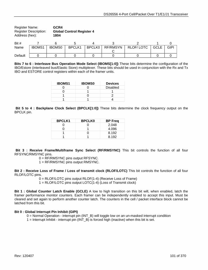
DS26556 4-Port Cell/Packet Over T1/E1/J1 Transceiver
Rev: 120407 101 of 370
Register Name: GCR4 Register Description: Global Control Register 4 Address (hex): 1804 Bit # 7 6 5 4 3 2 1 0 Name IBOMS1 IBOMS0 BPCLK1 BPCLK0 RF/RMSYN
C RLOF/ LOTC GCLE GIPI
Default 0 0 0 0 0 0 0 0 Bits 7 to 6 : Interleave Bus Operation Mode Select (IBOMS[1:0]) These bits determine the configuration of the IBO/Estore (interleaved bus/Elastic Store) multiplexer. These bits should be used in conjunction with the Rx and Tx IBO and ESTORE control registers within each of the framer units.
IBOMS1 IBOMS0 Devices 0 0 Disabled 0 1 1 1 0 2 1 1 4
Bit 5 to 4 : Backplane Clock Select (BPCLK[1:0]) These bits determine the clock frequency output on the BPCLK pin.
BPCLK1 BPCLK0 BP Freq 0 0 2.048 0 1 4.096 1 0 8.192 1 1 8.192
Bit 3 : Receive Frame/Multiframe Sync Select (RF/RMSYNC) This bit controls the function of all four RFSYNC/RMSYNC pins. 0 = RF/RMSYNC pins output RFSYNC. 1 = RF/RMSYNC pins output RMSYNC. Bit 2 : Receive Loss of Frame / Loss of transmit clock (RLOF/LOTC) This bit controls the function of all four RLOF/LOTC pins. 0 = RLOF/LOTC pins output RLOF(1-4) (Receive Loss of Frame) 1 = RLOF/LOTC pins output LOTC(1-4) (Loss of Transmit clock) Bit 1 : Global Counter Latch Enable (GCLE) A low to high transition on this bit will, when enabled, latch the framer performance monitor counters. Each framer can be independently enabled to accept this input. Must be cleared and set again to perform another counter latch. The counters in the cell / packet interface block cannot be latched from this bit. Bit 0 : Global Interrupt Pin Inhibit (GIPI) 0 = Normal Operation - interrupt pin (INT_B) will toggle low on an un-masked interrupt condition 1 = Interrupt Inhibit - interrupt pin (INT_B) is forced high (inactive) when this bit is set.
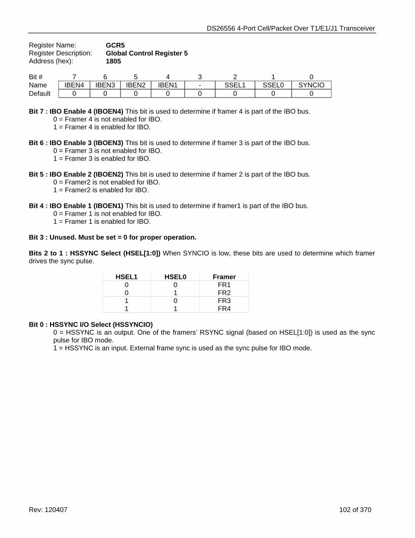
DS26556 4-Port Cell/Packet Over T1/E1/J1 Transceiver
Rev: 120407 102 of 370
Register Name: GCR5 Register Description: Global Control Register 5 Address (hex): 1805 Bit # 7 6 5 4 3 2 1 0 Name IBEN4 IBEN3 IBEN2 IBEN1 - SSEL1 SSEL0 SYNCIO Default 0 0 0 0 0 0 0 0 Bit 7 : IBO Enable 4 (IBOEN4) This bit is used to determine if framer 4 is part of the IBO bus. 0 = Framer 4 is not enabled for IBO. 1 = Framer 4 is enabled for IBO. Bit 6 : IBO Enable 3 (IBOEN3) This bit is used to determine if framer 3 is part of the IBO bus. 0 = Framer 3 is not enabled for IBO. 1 = Framer 3 is enabled for IBO. Bit 5 : IBO Enable 2 (IBOEN2) This bit is used to determine if framer 2 is part of the IBO bus. 0 = Framer2 is not enabled for IBO. 1 = Framer2 is enabled for IBO. Bit 4 : IBO Enable 1 (IBOEN1) This bit is used to determine if framer1 is part of the IBO bus. 0 = Framer 1 is not enabled for IBO. 1 = Framer 1 is enabled for IBO. Bit 3 : Unused. Must be set = 0 for proper operation. Bits 2 to 1 : HSSYNC Select (HSEL[1:0]) When SYNCIO is low, these bits are used to determine which framer drives the sync pulse.
HSEL1 HSEL0 Framer 0 0 FR1 0 1 FR2 1 0 FR3 1 1 FR4
Bit 0 : HSSYNC I/O Select (HSSYNCIO)
0 = HSSYNC is an output. One of the framers’ RSYNC signal (based on HSEL[1:0]) is used as the sync pulse for IBO mode.
1 = HSSYNC is an input. External frame sync is used as the sync pulse for IBO mode.
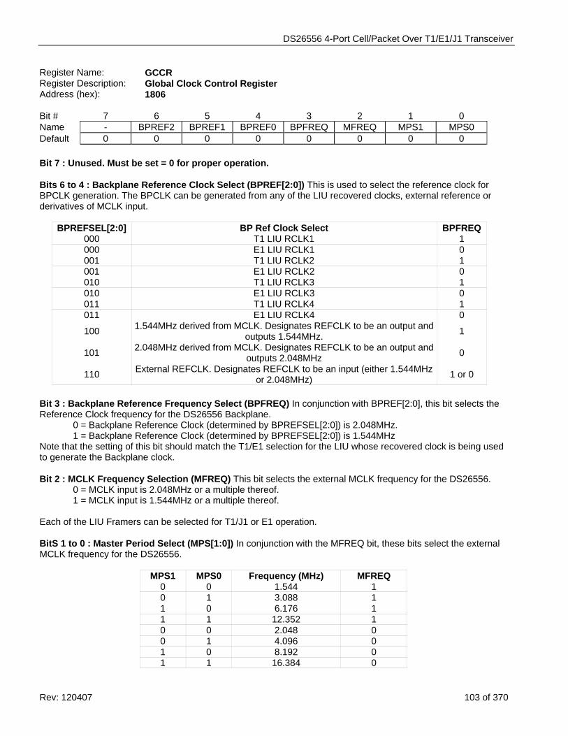
DS26556 4-Port Cell/Packet Over T1/E1/J1 Transceiver
Rev: 120407 103 of 370
Register Name: GCCR Register Description: Global Clock Control Register Address (hex): 1806 Bit # 7 6 5 4 3 2 1 0 Name - BPREF2 BPREF1 BPREF0 BPFREQ MFREQ MPS1 MPS0 Default 0 0 0 0 0 0 0 0 Bit 7 : Unused. Must be set = 0 for proper operation. Bits 6 to 4 : Backplane Reference Clock Select (BPREF[2:0]) This is used to select the reference clock for BPCLK generation. The BPCLK can be generated from any of the LIU recovered clocks, external reference or derivatives of MCLK input.
BPREFSEL[2:0] BP Ref Clock Select BPFREQ 000 T1 LIU RCLK1 1 000 E1 LIU RCLK1 0 001 T1 LIU RCLK2 1 001 E1 LIU RCLK2 0 010 T1 LIU RCLK3 1 010 E1 LIU RCLK3 0 011 T1 LIU RCLK4 1 011 E1 LIU RCLK4 0
100 1.544MHz derived from MCLK. Designates REFCLK to be an output and outputs 1.544MHz. 1
101 2.048MHz derived from MCLK. Designates REFCLK to be an output and outputs 2.048MHz 0
110 External REFCLK. Designates REFCLK to be an input (either 1.544MHz or 2.048MHz) 1 or 0
Bit 3 : Backplane Reference Frequency Select (BPFREQ) In conjunction with BPREF[2:0], this bit selects the Reference Clock frequency for the DS26556 Backplane. 0 = Backplane Reference Clock (determined by BPREFSEL[2:0]) is 2.048MHz. 1 = Backplane Reference Clock (determined by BPREFSEL[2:0]) is 1.544MHz Note that the setting of this bit should match the T1/E1 selection for the LIU whose recovered clock is being used to generate the Backplane clock. Bit 2 : MCLK Frequency Selection (MFREQ) This bit selects the external MCLK frequency for the DS26556. 0 = MCLK input is 2.048MHz or a multiple thereof. 1 = MCLK input is 1.544MHz or a multiple thereof. Each of the LIU Framers can be selected for T1/J1 or E1 operation. BitS 1 to 0 : Master Period Select (MPS[1:0]) In conjunction with the MFREQ bit, these bits select the external MCLK frequency for the DS26556.
MPS1 MPS0 Frequency (MHz) MFREQ 0 0 1.544 1 0 1 3.088 1 1 0 6.176 1 1 1 12.352 1 0 0 2.048 0 0 1 4.096 0 1 0 8.192 0 1 1 16.384 0
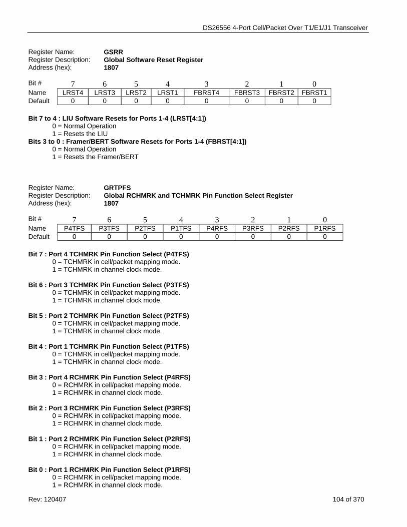
DS26556 4-Port Cell/Packet Over T1/E1/J1 Transceiver
Rev: 120407 104 of 370
Register Name: GSRR Register Description: Global Software Reset Register Address (hex): 1807 Bit # 7 6 5 4 3 2 1 0 Name LRST4 LRST3 LRST2 LRST1 FBRST4 FBRST3 FBRST2 FBRST1 Default 0 0 0 0 0 0 0 0 Bit 7 to 4 : LIU Software Resets for Ports 1-4 (LRST[4:1]) 0 = Normal Operation 1 = Resets the LIU Bits 3 to 0 : Framer/BERT Software Resets for Ports 1-4 (FBRST[4:1]) 0 = Normal Operation 1 = Resets the Framer/BERT Register Name: GRTPFS Register Description: Global RCHMRK and TCHMRK Pin Function Select Register Address (hex): 1807 Bit # 7 6 5 4 3 2 1 0 Name P4TFS P3TFS P2TFS P1TFS P4RFS P3RFS P2RFS P1RFS Default 0 0 0 0 0 0 0 0 Bit 7 : Port 4 TCHMRK Pin Function Select (P4TFS) 0 = TCHMRK in cell/packet mapping mode. 1 = TCHMRK in channel clock mode. Bit 6 : Port 3 TCHMRK Pin Function Select (P3TFS) 0 = TCHMRK in cell/packet mapping mode. 1 = TCHMRK in channel clock mode. Bit 5 : Port 2 TCHMRK Pin Function Select (P2TFS) 0 = TCHMRK in cell/packet mapping mode. 1 = TCHMRK in channel clock mode. Bit 4 : Port 1 TCHMRK Pin Function Select (P1TFS)
0 = TCHMRK in cell/packet mapping mode. 1 = TCHMRK in channel clock mode. Bit 3 : Port 4 RCHMRK Pin Function Select (P4RFS) 0 = RCHMRK in cell/packet mapping mode. 1 = RCHMRK in channel clock mode. Bit 2 : Port 3 RCHMRK Pin Function Select (P3RFS) 0 = RCHMRK in cell/packet mapping mode. 1 = RCHMRK in channel clock mode. Bit 1 : Port 2 RCHMRK Pin Function Select (P2RFS) 0 = RCHMRK in cell/packet mapping mode. 1 = RCHMRK in channel clock mode. Bit 0 : Port 1 RCHMRK Pin Function Select (P1RFS) 0 = RCHMRK in cell/packet mapping mode. 1 = RCHMRK in channel clock mode.
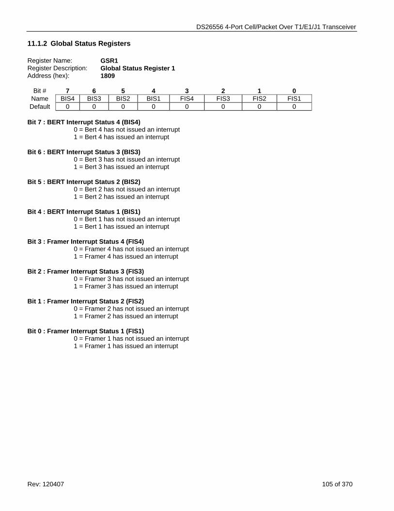
DS26556 4-Port Cell/Packet Over T1/E1/J1 Transceiver
Rev: 120407 105 of 370
11.1.2 Global Status Registers Register Name: GSR1 Register Description: Global Status Register 1 Address (hex): 1809
Bit # 7 6 5 4 3 2 1 0 Name BIS4 BIS3 BIS2 BIS1 FIS4 FIS3 FIS2 FIS1 Default 0 0 0 0 0 0 0 0
Bit 7 : BERT Interrupt Status 4 (BIS4) 0 = Bert 4 has not issued an interrupt 1 = Bert 4 has issued an interrupt Bit 6 : BERT Interrupt Status 3 (BIS3) 0 = Bert 3 has not issued an interrupt 1 = Bert 3 has issued an interrupt Bit 5 : BERT Interrupt Status 2 (BIS2) 0 = Bert 2 has not issued an interrupt 1 = Bert 2 has issued an interrupt Bit 4 : BERT Interrupt Status 1 (BIS1) 0 = Bert 1 has not issued an interrupt 1 = Bert 1 has issued an interrupt Bit 3 : Framer Interrupt Status 4 (FIS4) 0 = Framer 4 has not issued an interrupt 1 = Framer 4 has issued an interrupt Bit 2 : Framer Interrupt Status 3 (FIS3) 0 = Framer 3 has not issued an interrupt 1 = Framer 3 has issued an interrupt Bit 1 : Framer Interrupt Status 2 (FIS2) 0 = Framer 2 has not issued an interrupt 1 = Framer 2 has issued an interrupt Bit 0 : Framer Interrupt Status 1 (FIS1) 0 = Framer 1 has not issued an interrupt 1 = Framer 1 has issued an interrupt
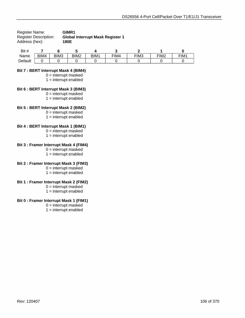
DS26556 4-Port Cell/Packet Over T1/E1/J1 Transceiver
Rev: 120407 106 of 370
Register Name: GIMR1 Register Description: Global Interrupt Mask Register 1 Address (hex): 180E
Bit # 7 6 5 4 3 2 1 0 Name BIM4 BIM3 BIM2 BIM1 FIM4 FIM3 FIM2 FIM1 Default 0 0 0 0 0 0 0 0
Bit 7 : BERT Interrupt Mask 4 (BIM4)
0 = interrupt masked 1 = interrupt enabled
Bit 6 : BERT Interrupt Mask 3 (BIM3)
0 = interrupt masked 1 = interrupt enabled
Bit 5 : BERT Interrupt Mask 2 (BIM2)
0 = interrupt masked 1 = interrupt enabled
Bit 4 : BERT Interrupt Mask 1 (BIM1)
0 = interrupt masked 1 = interrupt enabled
Bit 3 : Framer Interrupt Mask 4 (FIM4)
0 = interrupt masked 1 = interrupt enabled
Bit 2 : Framer Interrupt Mask 3 (FIM3)
0 = interrupt masked 1 = interrupt enabled
Bit 1 : Framer Interrupt Mask 2 (FIM2)
0 = interrupt masked 1 = interrupt enabled
Bit 0 : Framer Interrupt Mask 1 (FIM1)
0 = interrupt masked 1 = interrupt enabled
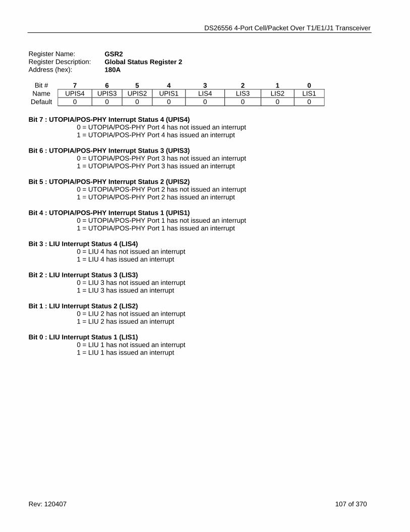
DS26556 4-Port Cell/Packet Over T1/E1/J1 Transceiver
Rev: 120407 107 of 370
Register Name: GSR2 Register Description: Global Status Register 2 Address (hex): 180A
Bit # 7 6 5 4 3 2 1 0
Name UPIS4 UPIS3 UPIS2 UPIS1 LIS4 LIS3 LIS2 LIS1 Default 0 0 0 0 0 0 0 0 Bit 7 : UTOPIA/POS-PHY Interrupt Status 4 (UPIS4) 0 = UTOPIA/POS-PHY Port 4 has not issued an interrupt 1 = UTOPIA/POS-PHY Port 4 has issued an interrupt Bit 6 : UTOPIA/POS-PHY Interrupt Status 3 (UPIS3) 0 = UTOPIA/POS-PHY Port 3 has not issued an interrupt 1 = UTOPIA/POS-PHY Port 3 has issued an interrupt Bit 5 : UTOPIA/POS-PHY Interrupt Status 2 (UPIS2) 0 = UTOPIA/POS-PHY Port 2 has not issued an interrupt 1 = UTOPIA/POS-PHY Port 2 has issued an interrupt Bit 4 : UTOPIA/POS-PHY Interrupt Status 1 (UPIS1) 0 = UTOPIA/POS-PHY Port 1 has not issued an interrupt 1 = UTOPIA/POS-PHY Port 1 has issued an interrupt Bit 3 : LIU Interrupt Status 4 (LIS4) 0 = LIU 4 has not issued an interrupt 1 = LIU 4 has issued an interrupt Bit 2 : LIU Interrupt Status 3 (LIS3) 0 = LIU 3 has not issued an interrupt 1 = LIU 3 has issued an interrupt Bit 1 : LIU Interrupt Status 2 (LIS2) 0 = LIU 2 has not issued an interrupt 1 = LIU 2 has issued an interrupt Bit 0 : LIU Interrupt Status 1 (LIS1) 0 = LIU 1 has not issued an interrupt 1 = LIU 1 has issued an interrupt
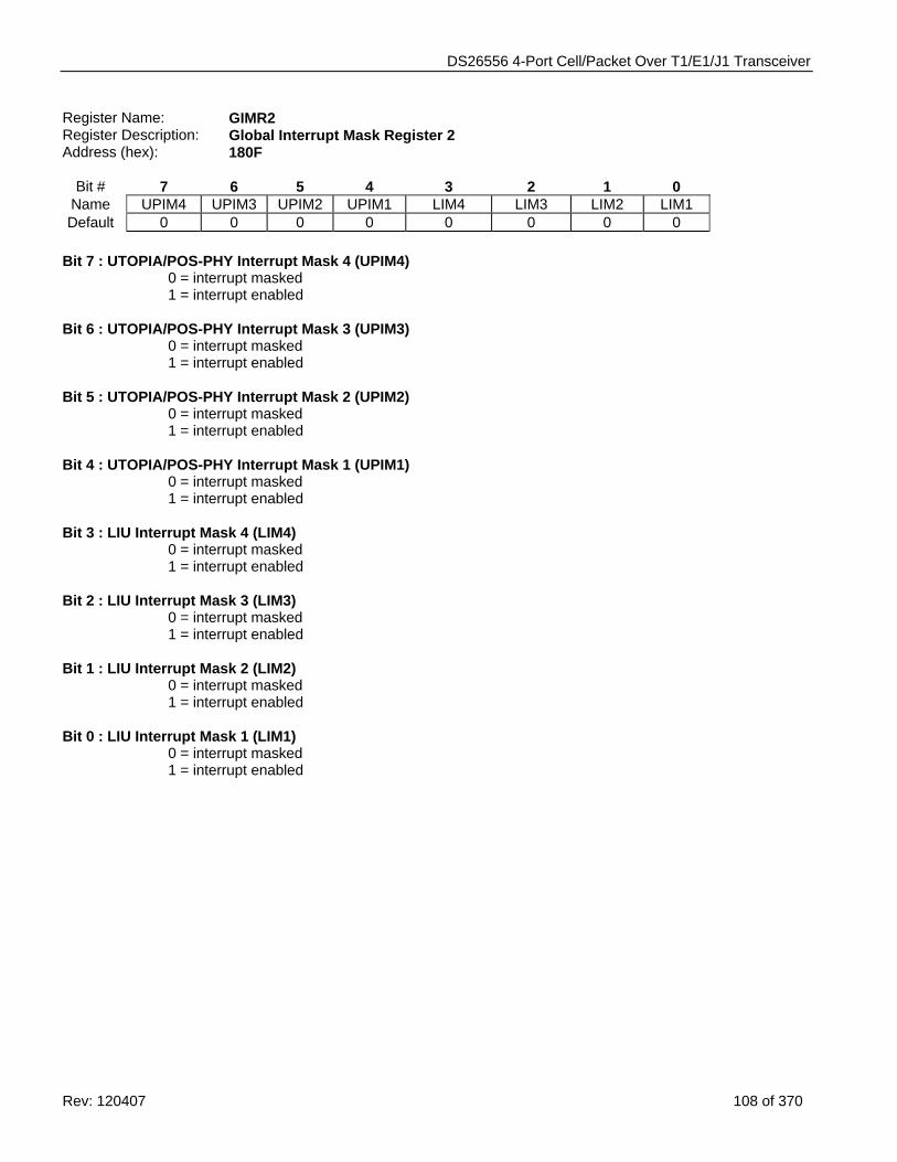
DS26556 4-Port Cell/Packet Over T1/E1/J1 Transceiver
Rev: 120407 108 of 370
Register Name: GIMR2 Register Description: Global Interrupt Mask Register 2 Address (hex): 180F
Bit # 7 6 5 4 3 2 1 0
Name UPIM4 UPIM3 UPIM2 UPIM1 LIM4 LIM3 LIM2 LIM1 Default 0 0 0 0 0 0 0 0 Bit 7 : UTOPIA/POS-PHY Interrupt Mask 4 (UPIM4)
0 = interrupt masked 1 = interrupt enabled
Bit 6 : UTOPIA/POS-PHY Interrupt Mask 3 (UPIM3)
0 = interrupt masked 1 = interrupt enabled
Bit 5 : UTOPIA/POS-PHY Interrupt Mask 2 (UPIM2)
0 = interrupt masked 1 = interrupt enabled
Bit 4 : UTOPIA/POS-PHY Interrupt Mask 1 (UPIM1)
0 = interrupt masked 1 = interrupt enabled
Bit 3 : LIU Interrupt Mask 4 (LIM4)
0 = interrupt masked 1 = interrupt enabled
Bit 2 : LIU Interrupt Mask 3 (LIM3)
0 = interrupt masked 1 = interrupt enabled
Bit 1 : LIU Interrupt Mask 2 (LIM2)
0 = interrupt masked 1 = interrupt enabled
Bit 0 : LIU Interrupt Mask 1 (LIM1)
0 = interrupt masked 1 = interrupt enabled
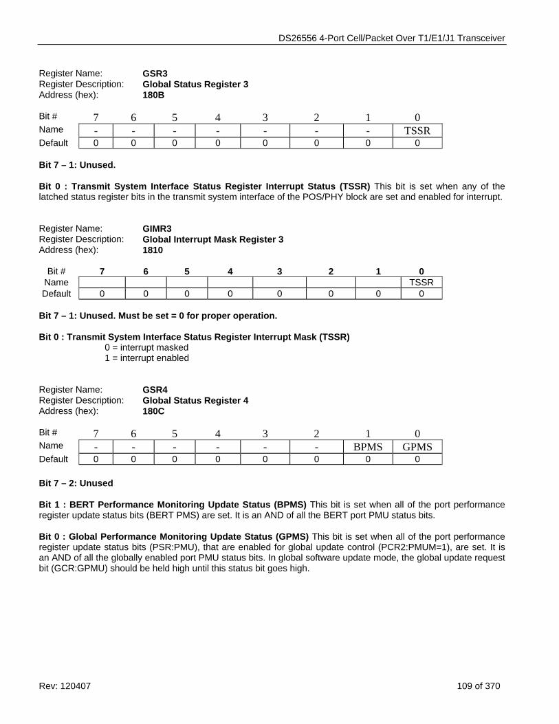
DS26556 4-Port Cell/Packet Over T1/E1/J1 Transceiver
Rev: 120407 109 of 370
Register Name: GSR3 Register Description: Global Status Register 3 Address (hex): 180B Bit # 7 6 5 4 3 2 1 0 Name - - - - - - - TSSR Default 0 0 0 0 0 0 0 0 Bit 7 – 1: Unused. Bit 0 : Transmit System Interface Status Register Interrupt Status (TSSR) This bit is set when any of the latched status register bits in the transmit system interface of the POS/PHY block are set and enabled for interrupt. Register Name: GIMR3 Register Description: Global Interrupt Mask Register 3 Address (hex): 1810
Bit # 7 6 5 4 3 2 1 0
Name TSSR Default 0 0 0 0 0 0 0 0
Bit 7 – 1: Unused. Must be set = 0 for proper operation. Bit 0 : Transmit System Interface Status Register Interrupt Mask (TSSR)
0 = interrupt masked 1 = interrupt enabled
Register Name: GSR4 Register Description: Global Status Register 4 Address (hex): 180C Bit # 7 6 5 4 3 2 1 0 Name - - - - - - BPMS GPMS Default 0 0 0 0 0 0 0 0 Bit 7 – 2: Unused Bit 1 : BERT Performance Monitoring Update Status (BPMS) This bit is set when all of the port performance register update status bits (BERT PMS) are set. It is an AND of all the BERT port PMU status bits. Bit 0 : Global Performance Monitoring Update Status (GPMS) This bit is set when all of the port performance register update status bits (PSR:PMU), that are enabled for global update control (PCR2:PMUM=1), are set. It is an AND of all the globally enabled port PMU status bits. In global software update mode, the global update request bit (GCR:GPMU) should be held high until this status bit goes high.
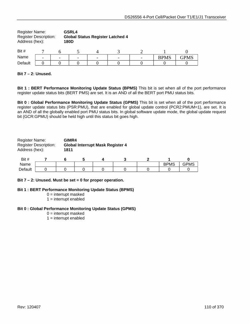
DS26556 4-Port Cell/Packet Over T1/E1/J1 Transceiver
Rev: 120407 110 of 370
Register Name: GSRL4 Register Description: Global Status Register Latched 4 Address (hex): 180D Bit # 7 6 5 4 3 2 1 0 Name - - - - - - BPMS GPMS Default 0 0 0 0 0 0 0 0 Bit 7 – 2: Unused. Bit 1 : BERT Performance Monitoring Update Status (BPMS) This bit is set when all of the port performance register update status bits (BERT PMS) are set. It is an AND of all the BERT port PMU status bits. Bit 0 : Global Performance Monitoring Update Status (GPMS) This bit is set when all of the port performance register update status bits (PSR:PMU), that are enabled for global update control (PCR2:PMUM=1), are set. It is an AND of all the globally enabled port PMU status bits. In global software update mode, the global update request bit (GCR:GPMU) should be held high until this status bit goes high. Register Name: GIMR4 Register Description: Global Interrupt Mask Register 4 Address (hex): 1811
Bit # 7 6 5 4 3 2 1 0
Name BPMS GPMS Default 0 0 0 0 0 0 0 0 Bit 7 – 2: Unused. Must be set = 0 for proper operation. Bit 1 : BERT Performance Monitoring Update Status (BPMS)
0 = interrupt masked 1 = interrupt enabled
Bit 0 : Global Performance Monitoring Update Status (GPMS)
0 = interrupt masked 1 = interrupt enabled
DS26556 4-Port Cell/Packet Over T1/E1/J1 Transceiver
Rev: 120407 111 of 370
11.2 Cell/Packet Register Descriptions The register descriptions are divided into separate register block sections. Bits that are underlined are read-only; all other bits are read-write. Configuration registers and bits can be written to and read from during a data path reset (LDRST bit = 0), however, all changes to these bits will be ignored during the data path reset. As a result, all bits requiring a 0 to 1 transition to initiate an action must have the transition occur after the data path reset has been removed.
All counters stop counting at their maximum count. A counter register is updated by asserting (low to high transition) the associated performance monitoring update signal (xxPMU). During the counter register update process, the associated performance monitoring status signal (xxPMS) will be deasserted. The counter register update process consists of loading the counter register with the current count, resetting the counter, forcing the zero count status indication low for one clock cycle, and then asserting xxPMS. No events shall be missed during an update procedure.
A latched bit is set when the associated event occurs, and remains set until it is cleared. Once cleared, a latched bit will not be set again until the associated event reoccurs (goes away and comes back). A latched on change bit is a latched bit that is set when the event occurs, and when it goes away. A latched status bit is cleared when the register is selected (register addressed and associated BSxx high), the appropriate byte enable (LBE or UBE) is high, a logic one is present on the corresponding DI[x], and the LSRCK signal goes high.
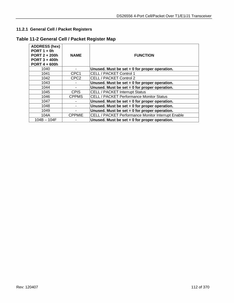
DS26556 4-Port Cell/Packet Over T1/E1/J1 Transceiver
Rev: 120407 112 of 370
11.2.1 General Cell / Packet Registers
Table 11-2 General Cell / Packet Register Map ADDRESS (hex) PORT 1 + 0h PORT 2 + 200h PORT 3 + 400h PORT 4 + 600h
NAME
FUNCTION
1040 - Unused. Must be set = 0 for proper operation. 1041 CPC1 CELL / PACKET Control 1 1042 CPC2 CELL / PACKET Control 2 1043 - Unused. Must be set = 0 for proper operation. 1044 - Unused. Must be set = 0 for proper operation. 1045 CPIS CELL / PACKET Interrupt Status 1046 CPPMS CELL / PACKET Performance Monitor Status 1047 - Unused. Must be set = 0 for proper operation. 1048 - Unused. Must be set = 0 for proper operation. 1049 - Unused. Must be set = 0 for proper operation. 104A CPPMIE CELL / PACKET Performance Monitor Interrupt Enable
104B – 104F - Unused. Must be set = 0 for proper operation.
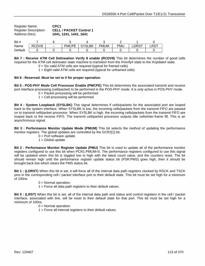
DS26556 4-Port Cell/Packet Over T1/E1/J1 Transceiver
Rev: 120407 113 of 370
Register Name: CPC1 Register Description: CELL / PACKET Control 1 Address (hex): 1041, 1241, 1441, 1641 Bit # 7 6 5 4 3 2 1 0 Name RCDV8 -- PMCPE SYSLBK PMUM PMU LDRST LRST Default 0 0 0 0 0 0 0 0 Bit 7 : Receive ATM Cell Delineation Verify 8 enable (RCDV8) This bit determines the number of good cells required for the ATM cell delineator state machine to transition from the #Verify# state to the #Update# state. 0 = Six valid ATM cells are required (typical for framed cells) 1 = Eight valid ATM cells are required (typical for unframed cells) Bit 6 : Reserved. Must be set to 0 for proper operation. Bit 5 : POS-PHY Mode Cell Processor Enable (PMCPE) This bit determines the associated transmit and receive port interface processing (cell/packet) to be performed in the POS-PHY mode. It is only active in POS-PHY mode. 0 = Packet processing will be performed 1 = Cell processing will be performed Bit 4 : System Loopback (SYSLBK) This signal determines if cells/packets for the associated port are looped back to the system interface. When SYSLBK is low, the incoming cells/packets from the transmit FIFO are passed on to transmit cell/packet processor. When SYSLBK is high, the incoming cells/packets from the transmit FIFO are looped back to the receive FIFO. The transmit cell/packet processor outputs idle cells/inter-frame fill. This is an asynchronous signal. Bit 3 : Performance Monitor Update Mode (PMUM) This bit selects the method of updating the performance monitor registers. The global updates are controlled by the GCR2[1] bit. 0 = Port software update 1 = Global update Bit 2 : Performance Monitor Register Update (PMU) This bit is used to update all of the performance monitor registers configured to use this bit when PCR1:PMUM=0. The performance registers configured to use this signal will be updated when this bit is toggled low to high with the latest count value, and the counters reset. The bit should remain high until the performance register update status bit (PSR:PMS) goes high, then it should be brought back low which clears the PMS status bit. Bit 1 : (LDRST) When this bit is set, it will force all of the internal data path registers clocked by RSCK and TSCK pins in the corresponding cell / packet interface port to their default state. This bit must be set high for a minimum of 100ns. 0 = Normal operation. 1 = Force all data path registers to their default values. Bit 0 : (LRST) When this bit is set, all of the internal data path and status and control registers in the cell / packet interface, associated with line, will be reset to their default state for that port. This bit must be set high for a minimum of 100ns. 0 = Normal operation. 1 = Force all internal registers to their default values.
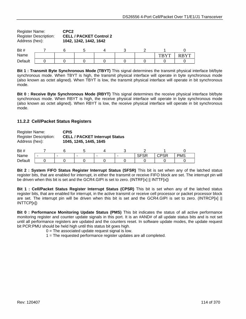
DS26556 4-Port Cell/Packet Over T1/E1/J1 Transceiver
Rev: 120407 114 of 370
Register Name: CPC2 Register Description: CELL / PACKET Control 2 Address (hex): 1042, 1242, 1442, 1642 Bit # 7 6 5 4 3 2 1 0 Name TBYT RBYT Default 0 0 0 0 0 0 0 0 Bit 1 : Transmit Byte Synchronous Mode (TBYT) This signal determines the transmit physical interface bit/byte synchronous mode. When TBYT is high, the transmit physical interface will operate in byte synchronous mode (also known as octet aligned). When TBYT is low, the transmit physical interface will operate in bit synchronous mode. Bit 0 : Receive Byte Synchronous Mode (RBYT) This signal determines the receive physical interface bit/byte synchronous mode. When RBYT is high, the receive physical interface will operate in byte synchronous mode (also known as octet aligned). When RBYT is low, the receive physical interface will operate in bit synchronous mode.
11.2.2 Cell/Packet Status Registers Register Name: CPIS Register Description: CELL / PACKET Interrupt Status Address (hex): 1045, 1245, 1445, 1645 Bit # 7 6 5 4 3 2 1 0 Name - - - - - SFSR CPSR PMS Default 0 0 0 0 0 0 0 0 Bit 2 : System FIFO Status Register Interrupt Status (SFSR) This bit is set when any of the latched status register bits, that are enabled for interrupt, in either the transmit or receive FIFO block are set. The interrupt pin will be driven when this bit is set and the GCR4.GIPI is set to zero. (INTRF[x] || INTTF[x]) Bit 1 : Cell/Packet Status Register Interrupt Status (CPSR) This bit is set when any of the latched status register bits, that are enabled for interrupt, in the active transmit or receive cell processor or packet processor block are set. The interrupt pin will be driven when this bit is set and the GCR4.GIPI is set to zero. (INTRCP[x] || INTTCP[x]) Bit 0 : Performance Monitoring Update Status (PMS) This bit indicates the status of all active performance monitoring register and counter update signals in this port. It is an #AND# of all update status bits and is not set until all performance registers are updated and the counters reset. In software update modes, the update request bit PCR:PMU should be held high until this status bit goes high. 0 = The associated update request signal is low. 1 = The requested performance register updates are all completed.
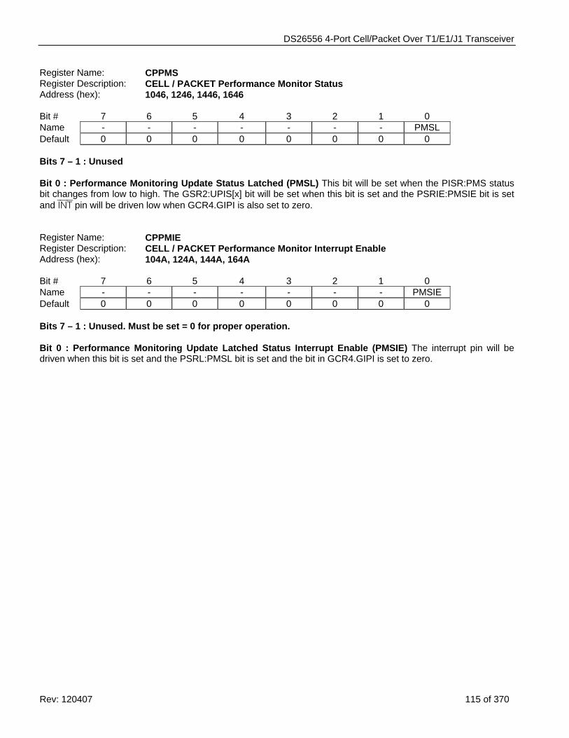
DS26556 4-Port Cell/Packet Over T1/E1/J1 Transceiver
Rev: 120407 115 of 370
Register Name: CPPMS Register Description: CELL / PACKET Performance Monitor Status Address (hex): 1046, 1246, 1446, 1646 Bit # 7 6 5 4 3 2 1 0 Name - - - - - - - PMSL Default 0 0 0 0 0 0 0 0 Bits 7 – 1 : Unused Bit 0 : Performance Monitoring Update Status Latched (PMSL) This bit will be set when the PISR:PMS status bit changes from low to high. The GSR2:UPIS[x] bit will be set when this bit is set and the PSRIE:PMSIE bit is set and INT pin will be driven low when GCR4.GIPI is also set to zero. Register Name: CPPMIE Register Description: CELL / PACKET Performance Monitor Interrupt Enable Address (hex): 104A, 124A, 144A, 164A Bit # 7 6 5 4 3 2 1 0 Name - - - - - - - PMSIE Default 0 0 0 0 0 0 0 0 Bits 7 – 1 : Unused. Must be set = 0 for proper operation. Bit 0 : Performance Monitoring Update Latched Status Interrupt Enable (PMSIE) The interrupt pin will be driven when this bit is set and the PSRL:PMSL bit is set and the bit in GCR4.GIPI is set to zero.
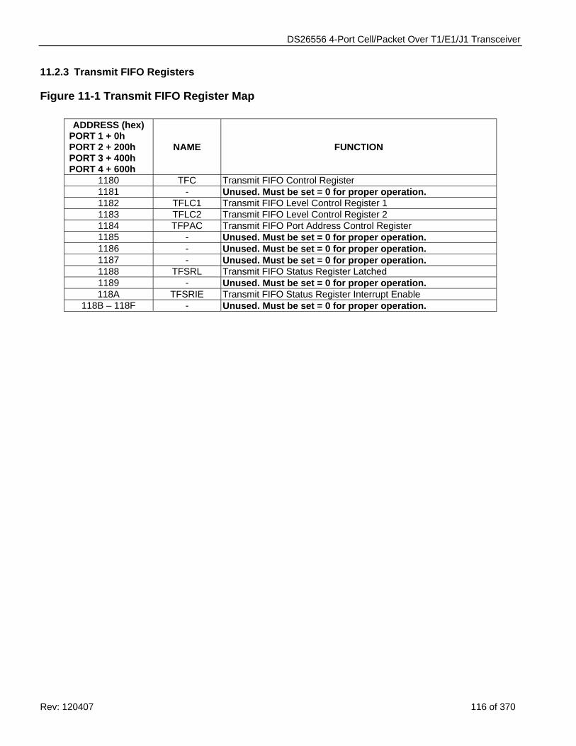
DS26556 4-Port Cell/Packet Over T1/E1/J1 Transceiver
Rev: 120407 116 of 370
11.2.3 Transmit FIFO Registers
Figure 11-1 Transmit FIFO Register Map
ADDRESS (hex) PORT 1 + 0h PORT 2 + 200h PORT 3 + 400h PORT 4 + 600h
NAME
FUNCTION
1180 TFC Transmit FIFO Control Register 1181 - Unused. Must be set = 0 for proper operation. 1182 TFLC1 Transmit FIFO Level Control Register 1 1183 TFLC2 Transmit FIFO Level Control Register 2 1184 TFPAC Transmit FIFO Port Address Control Register 1185 - Unused. Must be set = 0 for proper operation. 1186 - Unused. Must be set = 0 for proper operation. 1187 - Unused. Must be set = 0 for proper operation. 1188 TFSRL Transmit FIFO Status Register Latched 1189 - Unused. Must be set = 0 for proper operation. 118A TFSRIE Transmit FIFO Status Register Interrupt Enable
118B – 118F - Unused. Must be set = 0 for proper operation.
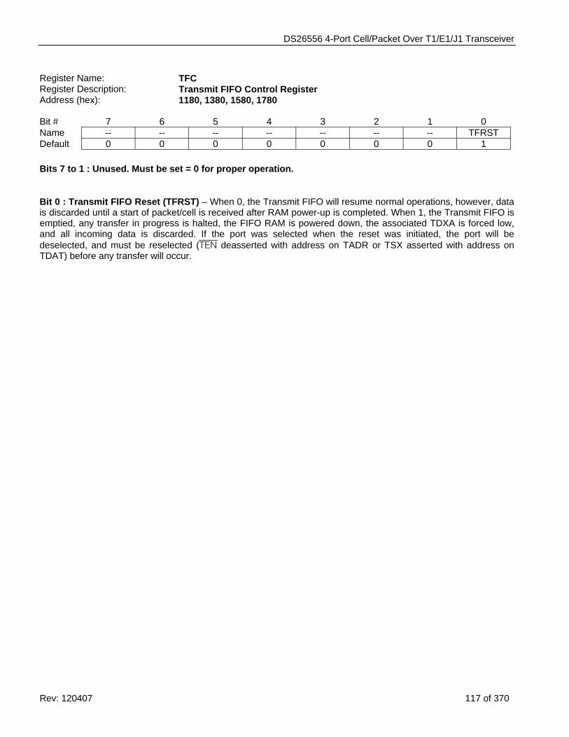
DS26556 4-Port Cell/Packet Over T1/E1/J1 Transceiver
Rev: 120407 117 of 370
Register Name: TFC Register Description: Transmit FIFO Control Register Address (hex): 1180, 1380, 1580, 1780 Bit # 7 6 5 4 3 2 1 0 Name -- -- -- -- -- -- -- TFRST Default 0 0 0 0 0 0 0 1 Bits 7 to 1 : Unused. Must be set = 0 for proper operation.
Bit 0 : Transmit FIFO Reset (TFRST) – When 0, the Transmit FIFO will resume normal operations, however, data is discarded until a start of packet/cell is received after RAM power-up is completed. When 1, the Transmit FIFO is emptied, any transfer in progress is halted, the FIFO RAM is powered down, the associated TDXA is forced low, and all incoming data is discarded. If the port was selected when the reset was initiated, the port will be deselected, and must be reselected (TEN deasserted with address on TADR or TSX asserted with address on TDAT) before any transfer will occur.
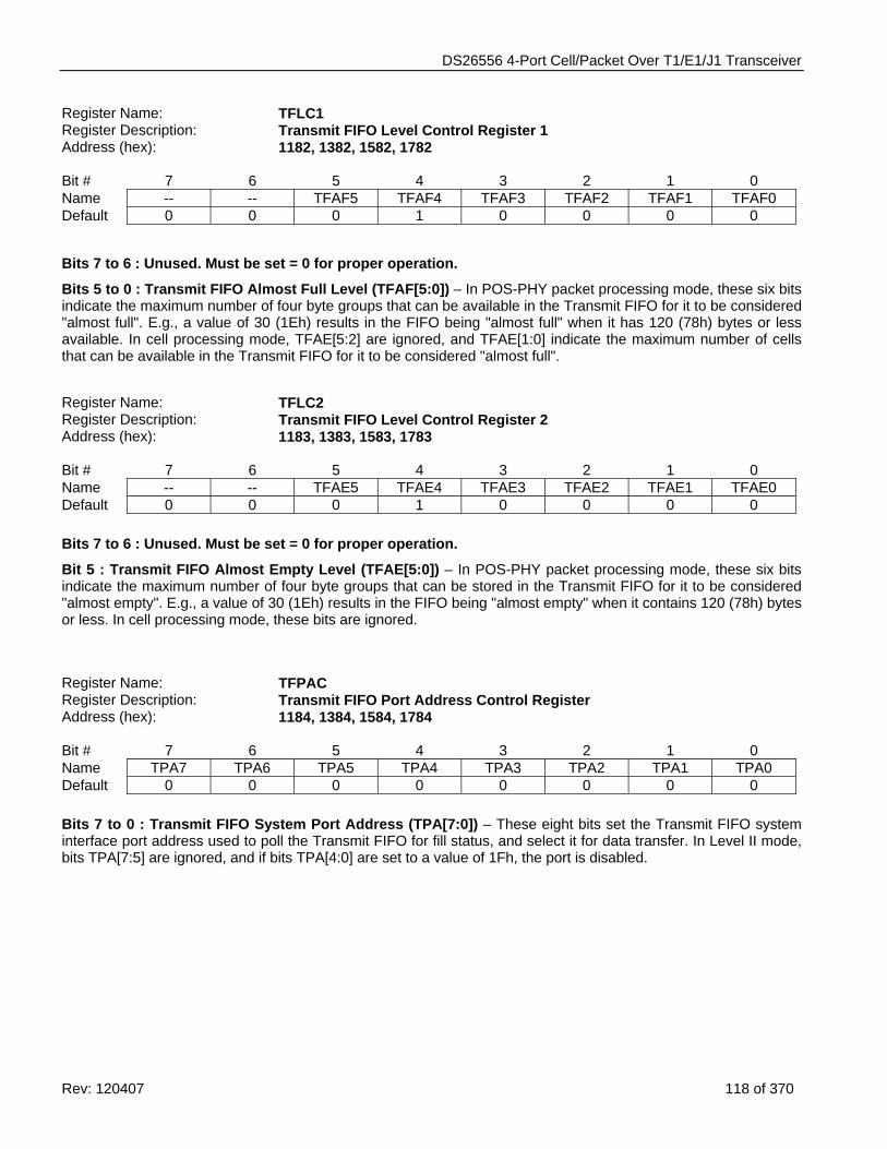
DS26556 4-Port Cell/Packet Over T1/E1/J1 Transceiver
Rev: 120407 118 of 370
Register Name: TFLC1 Register Description: Transmit FIFO Level Control Register 1 Address (hex): 1182, 1382, 1582, 1782 Bit # 7 6 5 4 3 2 1 0 Name -- -- TFAF5 TFAF4 TFAF3 TFAF2 TFAF1 TFAF0 Default 0 0 0 1 0 0 0 0
Bits 7 to 6 : Unused. Must be set = 0 for proper operation.
Bits 5 to 0 : Transmit FIFO Almost Full Level (TFAF[5:0]) – In POS-PHY packet processing mode, these six bits indicate the maximum number of four byte groups that can be available in the Transmit FIFO for it to be considered "almost full". E.g., a value of 30 (1Eh) results in the FIFO being "almost full" when it has 120 (78h) bytes or less available. In cell processing mode, TFAE[5:2] are ignored, and TFAE[1:0] indicate the maximum number of cells that can be available in the Transmit FIFO for it to be considered "almost full".
Register Name: TFLC2 Register Description: Transmit FIFO Level Control Register 2 Address (hex): 1183, 1383, 1583, 1783 Bit # 7 6 5 4 3 2 1 0 Name -- -- TFAE5 TFAE4 TFAE3 TFAE2 TFAE1 TFAE0 Default 0 0 0 1 0 0 0 0 Bits 7 to 6 : Unused. Must be set = 0 for proper operation.
Bit 5 : Transmit FIFO Almost Empty Level (TFAE[5:0]) – In POS-PHY packet processing mode, these six bits indicate the maximum number of four byte groups that can be stored in the Transmit FIFO for it to be considered "almost empty". E.g., a value of 30 (1Eh) results in the FIFO being "almost empty" when it contains 120 (78h) bytes or less. In cell processing mode, these bits are ignored. Register Name: TFPAC Register Description: Transmit FIFO Port Address Control Register Address (hex): 1184, 1384, 1584, 1784 Bit # 7 6 5 4 3 2 1 0 Name TPA7 TPA6 TPA5 TPA4 TPA3 TPA2 TPA1 TPA0 Default 0 0 0 0 0 0 0 0 Bits 7 to 0 : Transmit FIFO System Port Address (TPA[7:0]) – These eight bits set the Transmit FIFO system interface port address used to poll the Transmit FIFO for fill status, and select it for data transfer. In Level II mode, bits TPA[7:5] are ignored, and if bits TPA[4:0] are set to a value of 1Fh, the port is disabled.
DS26556 4-Port Cell/Packet Over T1/E1/J1 Transceiver
Rev: 120407 119 of 370
Register Name: TFSRL Register Description: Transmit FIFO Status Register Latched Address (hex): 1188, 1388, 1588, 1788 Bit # 7 6 5 4 3 2 1 0 Name -- -- -- TFATL TFSTL TFITL TFUL TFOL Default 0 0 0 0 0 0 0 0
Bits 7 to 5 : Unused.
Bit 4 : Transmit FIFO Aborted Transfer Latched (TFATL) – This bit is set when a transfer is aborted. An aborted transfer does not occur in UTOPIA mode. In POS-PHY mode, an aborted transfer occurs when a packet error (a transfer with TERR and TEOP asserted) occurs. An aborted transfer is stored in the transmit FIFO with an abort indication.
Bit 3 : Transmit FIFO Short Transfer Latched (TFSTL) – This bit is set when a "short transfer" is received. In UTOPIA mode, a "short transfer" occurs when a start of cell (a transfer with TSOC asserted) occurs before the previous cell transfer has been completed. In POS-PHY mode, a "short transfer" occurs when a start of packet (a transfer with TSOP asserted) occurs after a previous start of packet, but before an end of packet (a transfer with TEOP asserted). In UTOPIA mode, the short transfer data is discarded. In POS-PHY mode, a short transfer is stored in the transmit FIFO with an abort indication.
Bit 2 : Transmit FIFO Invalid Transfer Latched (TFITL) – This bit is set when an "invalid transfer" is initiated. In UTOPIA mode, an "invalid transfer" occurs when additional cell data is transferred after the last transfer of a cell and before a transfer with TSOC asserted. In POS-PHY mode, an "invalid transfer" occurs when packet data is transferred after an end of packet, but before a start of packet (this includes another end of packet transfer). The invalid transfer data is discarded.
Bit 1 : Transmit FIFO Underflow Latched (TFUL) – This bit is set when a Transmit FIFO underflow condition occurs. An underflow condition results in a loss of data.
Bit 0 : Transmit FIFO Overflow Latched (TFOL) – This bit is set when a Transmit FIFO overflow condition occurs. An overflow condition results in a loss of data.
DS26556 4-Port Cell/Packet Over T1/E1/J1 Transceiver
Rev: 120407 120 of 370
Register Name: TFSRIE Register Description: Transmit FIFO Status Register Interrupt Enable Address (hex): 118A, 138A, 158A, 178A Bit # 7 6 5 4 3 2 1 0 Name -- -- -- TFATIE TFSTIE TFITIE TFUIE TFOIE Default 0 0 0 0 0 0 0 0 Bits 7 to 5 : Unused. Must be set = 0 for proper operation.
Bit 4 : Transmit FIFO Aborted Transfer Interrupt Enable (TFATIE) – This bit enables an interrupt if the TFATL bit in the TFSRL register is set.
0 = interrupt disabled 1 = interrupt enabled
Bit 3 : Transmit FIFO Short Transfer Interrupt Enable (TFSTIE) – This bit enables an interrupt if the TFSTL bit in the TFSRL register is set.
0 = interrupt disabled 1 = interrupt enabled
Bit 2 : Transmit FIFO Invalid Transfer Interrupt Enable (TFITIE) – This bit enables an interrupt if the TFITL bit in the TFSRL register is set.
0 = interrupt disabled 1 = interrupt enabled
Bit 1 : Transmit FIFO Underflow Interrupt Enable (TFUIE) – This bit enables an interrupt if the TFUL bit in the TFSRL register is set.
0 = interrupt disabled 1 = interrupt enabled
Bit 0 : Transmit FIFO Overflow Interrupt Enable (TFOIE) – This bit enables an interrupt if the TFOL bit in the TFSRL register is set.
0 = interrupt disabled 1 = interrupt enabled
DS26556 4-Port Cell/Packet Over T1/E1/J1 Transceiver
Rev: 120407 121 of 370
11.2.4 Transmit Cell Processor Registers
Table 11-3 Transmit Cell Processor Register Map ADDRESS (hex)
PORT 1 + 0h PORT 2 + 200h PORT 3 + 400h PORT 4 + 600h
NAME
FUNCTION
1100 TCPC1 Transmit Cell Processor Control Register 1 1101 TCPC2 Transmit Cell Processor Control Register 2 1102 - Unused. Must be set = 0 for proper operation. 1103 - Unused. Must be set = 0 for proper operation. 1104 TECC1 Transmit Errored Cell Control Register 1 1105 TECC2 Transmit Errored Cell Control Register 2 1106 THMRC Transmit HEC Error Mask Control Register 1107 - Unused. Must be set = 0 for proper operation. 1108 THPC1 Transmit Header Pattern Control Register 1 1109 THPC2 Transmit Header Pattern Control Register 2 110A THPC3 Transmit Header Pattern Control Register 3 110B THPC4 Transmit Header Pattern Control Register 4 110C TFPPC Transmit Fill Cell Payload Pattern Control Register 110D - Unused. Must be set = 0 for proper operation. 110E TCPSR Transmit Cell Processor Status Register 110F - Unused. Must be set = 0 for proper operation. 1110 TCPSRL Transmit Cell Processor Status Register Latched 1111 - Unused. Must be set = 0 for proper operation. 1112 TCPSRIE Transmit Cell Processor Status Register Interrupt Enable 1113 - Unused. Must be set = 0 for proper operation. 1114 TCCR1 Transmit Cell Count Register 1 1115 TCCR2 Transmit Cell Count Register 2 1116 TCCR3 Transmit Cell Count Register 3
1117-111F - Unused. Must be set = 0 for proper operation.
DS26556 4-Port Cell/Packet Over T1/E1/J1 Transceiver
Rev: 120407 122 of 370
Register Name: TCPC1 Register Description: Transmit Cell Processor Control Register 1 Address (hex): 1100, 1300, 1500, 1700 Bit # 7 6 5 4 3 2 1 0 Name -- -- TFCH TFCP THSE TSD TBRE TCCE Default 0 0 0 0 0 0 0 0 Bits 7& 6 : Unused. Must be set = 0 for proper operation.
Bit 5 : Transmit Fill Cell Header Type (TFCH) – When 0, an idle cell header (00 00 00 01h) will be used in fill cells. When 1, a programmable header will be used in fill cells. The setting of this bit does not affect the contents of the cell payload bytes. Bit 4 : Transmit Fill Cell Payload Type (TFCP) – When 0, an idle cell payload byte (6Ah) will be used in each payload byte fill cells. When 1, a programmable cell payload byte will be used in each payload byte fill cells. The setting of this bit does not affect the contents of the cell header bytes. Bit 3 : Transmit Cell Header Scrambling Enable (THSE) – When 0, only the cell payload will be scrambled. When 1, the entire data stream (cell header and payload) is scrambled. This bit is ignored if scrambling is disabled, or DSS scrambling is enabled. When clear channel is enabled, the entire data stream will be scrambled if scrambling is enabled. Bit 2 : Transmit Scrambling Disable (TSD) – When 0, scrambling is performed. When 1, scrambling is disabled. Bit 1 : Transmit Bit Reordering Enable (TBRE) – When 0, bit reordering is disabled (The first bit transmitted is from the MSB of the transmit FIFO byte TFD[7]). When 1, bit reordering is enabled (The first bit transmitted is from the LSB of the transmit FIFO byte TFD[0]). Bit 0 : Transmit Clear Channel Enable (TCCE) – When 0, cell processing is enabled. When 1, clear channel is enabled, and all cell processing functions except scrambling and bit reordering are disabled.
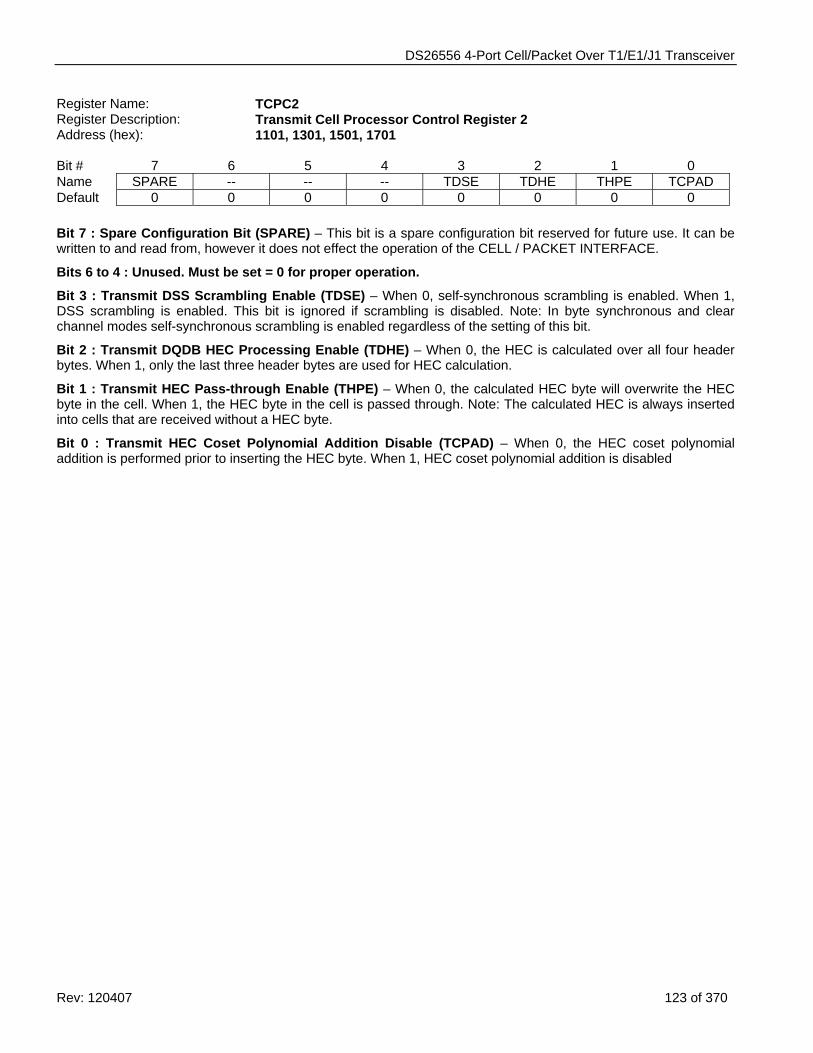
DS26556 4-Port Cell/Packet Over T1/E1/J1 Transceiver
Rev: 120407 123 of 370
Register Name: TCPC2 Register Description: Transmit Cell Processor Control Register 2 Address (hex): 1101, 1301, 1501, 1701 Bit # 7 6 5 4 3 2 1 0 Name SPARE -- -- -- TDSE TDHE THPE TCPAD Default 0 0 0 0 0 0 0 0 Bit 7 : Spare Configuration Bit (SPARE) – This bit is a spare configuration bit reserved for future use. It can be written to and read from, however it does not effect the operation of the CELL / PACKET INTERFACE.
Bits 6 to 4 : Unused. Must be set = 0 for proper operation.
Bit 3 : Transmit DSS Scrambling Enable (TDSE) – When 0, self-synchronous scrambling is enabled. When 1, DSS scrambling is enabled. This bit is ignored if scrambling is disabled. Note: In byte synchronous and clear channel modes self-synchronous scrambling is enabled regardless of the setting of this bit.
Bit 2 : Transmit DQDB HEC Processing Enable (TDHE) – When 0, the HEC is calculated over all four header bytes. When 1, only the last three header bytes are used for HEC calculation.
Bit 1 : Transmit HEC Pass-through Enable (THPE) – When 0, the calculated HEC byte will overwrite the HEC byte in the cell. When 1, the HEC byte in the cell is passed through. Note: The calculated HEC is always inserted into cells that are received without a HEC byte.
Bit 0 : Transmit HEC Coset Polynomial Addition Disable (TCPAD) – When 0, the HEC coset polynomial addition is performed prior to inserting the HEC byte. When 1, HEC coset polynomial addition is disabled
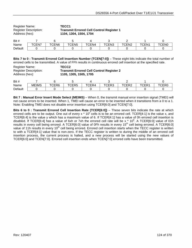
DS26556 4-Port Cell/Packet Over T1/E1/J1 Transceiver
Rev: 120407 124 of 370
Register Name: TECC1 Register Description: Transmit Errored Cell Control Register 1 Address (hex): 1104, 1304, 1504, 1704 Bit # 7 6 5 4 3 2 1 0 Name TCEN7 TCEN6 TCEN5 TCEN4 TCEN3 TCEN2 TCEN1 TCEN0 Default 0 0 0 0 0 0 0 0
Bits 7 to 0 : Transmit Errored Cell Insertion Number (TCEN[7:0]) – These eight bits indicate the total number of errored cells to be transmitted. A value of FFh results in continuous errored cell insertion at the specified rate. Register Name: TECC2 Register Description: Transmit Errored Cell Control Register 2 Address (hex): 1105, 1305, 1505, 1705 Bit # 7 6 5 4 3 2 1 0 Name MEIMS TCER6 TCER5 TCER4 TCER3 TCER2 TCER1 TCER0 Default 0 0 0 0 0 0 0 0 Bit 7 : Manual Error Insert Mode Select (MEIMS) – When 0, the transmit manual error insertion signal (TMEI) will not cause errors to be inserted. When 1, TMEI will cause an error to be inserted when it transitions from a 0 to a 1. Note: Enabling TMEI does not disable error insertion using TCER[6:0] and TCEN[7:0].
Bits 6 to 0 : Transmit Errored Cell Insertion Rate (TCER[6:0]) – These seven bits indicate the rate at which errored cells are to be output. One out of every x * 10y cells is to be an errored cell. TCER[4:1] is the value x, and TCER[6:4] is the value y which has a maximum value of 6. If TCER[4:1] has a value of 0h errored cell insertion is disabled. If TCER[6:4] has a value of 6xh or 7xh the errored cell rate will be x * 106. A TCER[6:0] value of 01h results in every cell being errored. A TCER[6:0] value of 0Fh results in every 15th cell being errored. A TCER[6:0] value of 11h results in every 10th cell being errored. Errored cell insertion starts when the TECC register is written to with a TCER[4:1] value that is non-zero. If the TECC register is written to during the middle of an errored cell insertion process, the current process is halted, and a new process will be started using the new values of TCER[6:0] and TCEN[7:0}. Errored cell insertion ends when TCEN[7:0] errored cells have been transmitted.
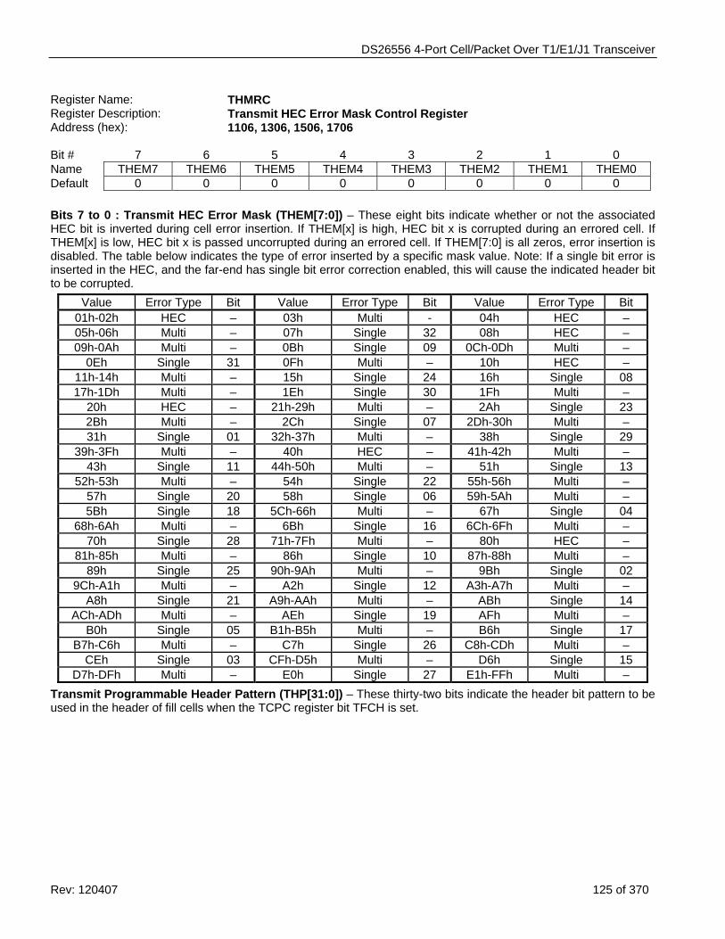
DS26556 4-Port Cell/Packet Over T1/E1/J1 Transceiver
Rev: 120407 125 of 370
Register Name: THMRC Register Description: Transmit HEC Error Mask Control Register Address (hex): 1106, 1306, 1506, 1706 Bit # 7 6 5 4 3 2 1 0 Name THEM7 THEM6 THEM5 THEM4 THEM3 THEM2 THEM1 THEM0 Default 0 0 0 0 0 0 0 0 Bits 7 to 0 : Transmit HEC Error Mask (THEM[7:0]) – These eight bits indicate whether or not the associated HEC bit is inverted during cell error insertion. If THEM[x] is high, HEC bit x is corrupted during an errored cell. If THEM[x] is low, HEC bit x is passed uncorrupted during an errored cell. If THEM[7:0] is all zeros, error insertion is disabled. The table below indicates the type of error inserted by a specific mask value. Note: If a single bit error is inserted in the HEC, and the far-end has single bit error correction enabled, this will cause the indicated header bit to be corrupted.
Value Error Type Bit Value Error Type Bit Value Error Type Bit 01h-02h HEC – 03h Multi - 04h HEC – 05h-06h Multi – 07h Single 32 08h HEC – 09h-0Ah Multi – 0Bh Single 09 0Ch-0Dh Multi –
0Eh Single 31 0Fh Multi – 10h HEC – 11h-14h Multi – 15h Single 24 16h Single 08 17h-1Dh Multi – 1Eh Single 30 1Fh Multi –
20h HEC – 21h-29h Multi – 2Ah Single 23 2Bh Multi – 2Ch Single 07 2Dh-30h Multi – 31h Single 01 32h-37h Multi – 38h Single 29
39h-3Fh Multi – 40h HEC – 41h-42h Multi – 43h Single 11 44h-50h Multi – 51h Single 13
52h-53h Multi – 54h Single 22 55h-56h Multi – 57h Single 20 58h Single 06 59h-5Ah Multi – 5Bh Single 18 5Ch-66h Multi – 67h Single 04
68h-6Ah Multi – 6Bh Single 16 6Ch-6Fh Multi – 70h Single 28 71h-7Fh Multi – 80h HEC –
81h-85h Multi – 86h Single 10 87h-88h Multi – 89h Single 25 90h-9Ah Multi – 9Bh Single 02
9Ch-A1h Multi – A2h Single 12 A3h-A7h Multi – A8h Single 21 A9h-AAh Multi – ABh Single 14
ACh-ADh Multi – AEh Single 19 AFh Multi – B0h Single 05 B1h-B5h Multi – B6h Single 17
B7h-C6h Multi – C7h Single 26 C8h-CDh Multi – CEh Single 03 CFh-D5h Multi – D6h Single 15
D7h-DFh Multi – E0h Single 27 E1h-FFh Multi – Transmit Programmable Header Pattern (THP[31:0]) – These thirty-two bits indicate the header bit pattern to be used in the header of fill cells when the TCPC register bit TFCH is set.
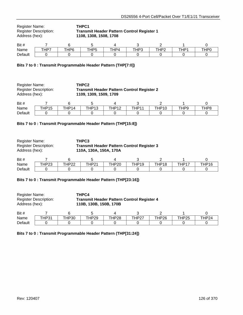
DS26556 4-Port Cell/Packet Over T1/E1/J1 Transceiver
Rev: 120407 126 of 370
Register Name: THPC1 Register Description: Transmit Header Pattern Control Register 1 Address (hex): 1108, 1308, 1508, 1708 Bit # 7 6 5 4 3 2 1 0 Name THP7 THP6 THP5 THP4 THP3 THP2 THP1 THP0 Default 0 0 0 0 0 0 0 0 Bits 7 to 0 : Transmit Programmable Header Pattern (THP[7:0])
Register Name: THPC2 Register Description: Transmit Header Pattern Control Register 2 Address (hex): 1109, 1309, 1509, 1709 Bit # 7 6 5 4 3 2 1 0 Name THP15 THP14 THP13 THP12 THP11 THP10 THP9 THP8 Default 0 0 0 0 0 0 0 0 Bits 7 to 0 : Transmit Programmable Header Pattern (THP[15:8])
Register Name: THPC3 Register Description: Transmit Header Pattern Control Register 3 Address (hex): 110A, 130A, 150A, 170A Bit # 7 6 5 4 3 2 1 0 Name THP23 THP22 THP21 THP20 THP19 THP18 THP17 THP16 Default 0 0 0 0 0 0 0 0 Bits 7 to 0 : Transmit Programmable Header Pattern (THP[23:16]) Register Name: THPC4 Register Description: Transmit Header Pattern Control Register 4 Address (hex): 110B, 130B, 150B, 170B Bit # 7 6 5 4 3 2 1 0 Name THP31 THP30 THP29 THP28 THP27 THP26 THP25 THP24 Default 0 0 0 0 0 0 0 0 Bits 7 to 0 : Transmit Programmable Header Pattern (THP[31:24])
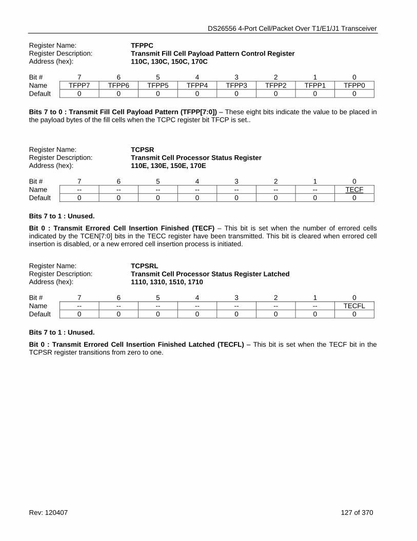
DS26556 4-Port Cell/Packet Over T1/E1/J1 Transceiver
Rev: 120407 127 of 370
Register Name: TFPPC Register Description: Transmit Fill Cell Payload Pattern Control Register Address (hex): 110C, 130C, 150C, 170C Bit # 7 6 5 4 3 2 1 0 Name TFPP7 TFPP6 TFPP5 TFPP4 TFPP3 TFPP2 TFPP1 TFPP0 Default 0 0 0 0 0 0 0 0 Bits 7 to 0 : Transmit Fill Cell Payload Pattern (TFPP[7:0]) – These eight bits indicate the value to be placed in the payload bytes of the fill cells when the TCPC register bit TFCP is set..
Register Name: TCPSR Register Description: Transmit Cell Processor Status Register Address (hex): 110E, 130E, 150E, 170E Bit # 7 6 5 4 3 2 1 0 Name -- -- -- -- -- -- -- TECF Default 0 0 0 0 0 0 0 0 Bits 7 to 1 : Unused.
Bit 0 : Transmit Errored Cell Insertion Finished (TECF) – This bit is set when the number of errored cells indicated by the TCEN[7:0] bits in the TECC register have been transmitted. This bit is cleared when errored cell insertion is disabled, or a new errored cell insertion process is initiated.
Register Name: TCPSRL Register Description: Transmit Cell Processor Status Register Latched Address (hex): 1110, 1310, 1510, 1710 Bit # 7 6 5 4 3 2 1 0 Name -- -- -- -- -- -- -- TECFL Default 0 0 0 0 0 0 0 0 Bits 7 to 1 : Unused.
Bit 0 : Transmit Errored Cell Insertion Finished Latched (TECFL) – This bit is set when the TECF bit in the TCPSR register transitions from zero to one.
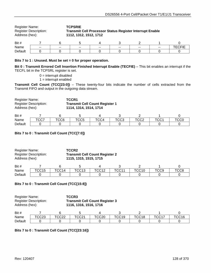
DS26556 4-Port Cell/Packet Over T1/E1/J1 Transceiver
Rev: 120407 128 of 370
Register Name: TCPSRIE Register Description: Transmit Cell Processor Status Register Interrupt Enable Address (hex): 1112, 1312, 1512, 1712 Bit # 7 6 5 4 3 2 1 0 Name -- -- -- -- -- -- -- TECFIE Default 0 0 0 0 0 0 0 0 Bits 7 to 1 : Unused. Must be set = 0 for proper operation.
Bit 0 : Transmit Errored Cell Insertion Finished Interrupt Enable (TECFIE) – This bit enables an interrupt if the TECFL bit in the TCPSRL register is set.
0 = interrupt disabled 1 = interrupt enabled
Transmit Cell Count (TCC[23:0]) – These twenty-four bits indicate the number of cells extracted from the Transmit FIFO and output in the outgoing data stream.
Register Name: TCCR1 Register Description: Transmit Cell Count Register 1 Address (hex): 1114, 1314, 1514, 1714 Bit # 7 6 5 4 3 2 1 0 Name TCC7 TCC6 TCC5 TCC4 TCC3 TCC2 TCC1 TCC0 Default 0 0 0 0 0 0 0 0 Bits 7 to 0 : Transmit Cell Count (TCC[7:0])
Register Name: TCCR2 Register Description: Transmit Cell Count Register 2 Address (hex): 1115, 1315, 1515, 1715 Bit # 7 6 5 4 3 2 1 0 Name TCC15 TCC14 TCC13 TCC12 TCC11 TCC10 TCC9 TCC8 Default 0 0 0 0 0 0 0 0 Bits 7 to 0 : Transmit Cell Count (TCC[15:8]) Register Name: TCCR3 Register Description: Transmit Cell Count Register 3 Address (hex): 1116, 1316, 1516, 1716 Bit # 7 6 5 4 3 2 1 0 Name TCC23 TCC22 TCC21 TCC20 TCC19 TCC18 TCC17 TCC16 Default 0 0 0 0 0 0 0 0 Bits 7 to 0 : Transmit Cell Count (TCC[23:16])
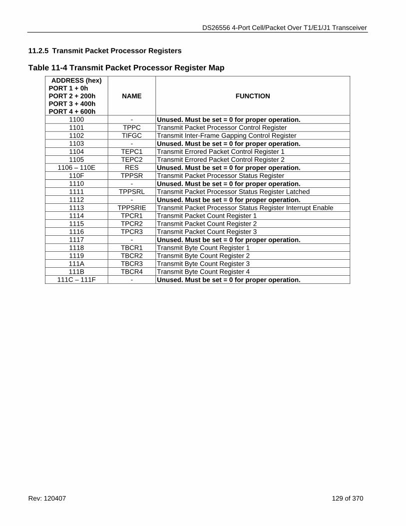
DS26556 4-Port Cell/Packet Over T1/E1/J1 Transceiver
Rev: 120407 129 of 370
11.2.5 Transmit Packet Processor Registers
Table 11-4 Transmit Packet Processor Register Map ADDRESS (hex)
PORT 1 + 0h PORT 2 + 200h PORT 3 + 400h PORT 4 + 600h
NAME
FUNCTION
1100 - Unused. Must be set = 0 for proper operation. 1101 TPPC Transmit Packet Processor Control Register 1102 TIFGC Transmit Inter-Frame Gapping Control Register 1103 - Unused. Must be set = 0 for proper operation. 1104 TEPC1 Transmit Errored Packet Control Register 1 1105 TEPC2 Transmit Errored Packet Control Register 2
1106 – 110E RES Unused. Must be set = 0 for proper operation. 110F TPPSR Transmit Packet Processor Status Register 1110 - Unused. Must be set = 0 for proper operation. 1111 TPPSRL Transmit Packet Processor Status Register Latched 1112 - Unused. Must be set = 0 for proper operation. 1113 TPPSRIE Transmit Packet Processor Status Register Interrupt Enable 1114 TPCR1 Transmit Packet Count Register 1 1115 TPCR2 Transmit Packet Count Register 2 1116 TPCR3 Transmit Packet Count Register 3 1117 - Unused. Must be set = 0 for proper operation. 1118 TBCR1 Transmit Byte Count Register 1 1119 TBCR2 Transmit Byte Count Register 2 111A TBCR3 Transmit Byte Count Register 3 111B TBCR4 Transmit Byte Count Register 4
111C – 111F - Unused. Must be set = 0 for proper operation.
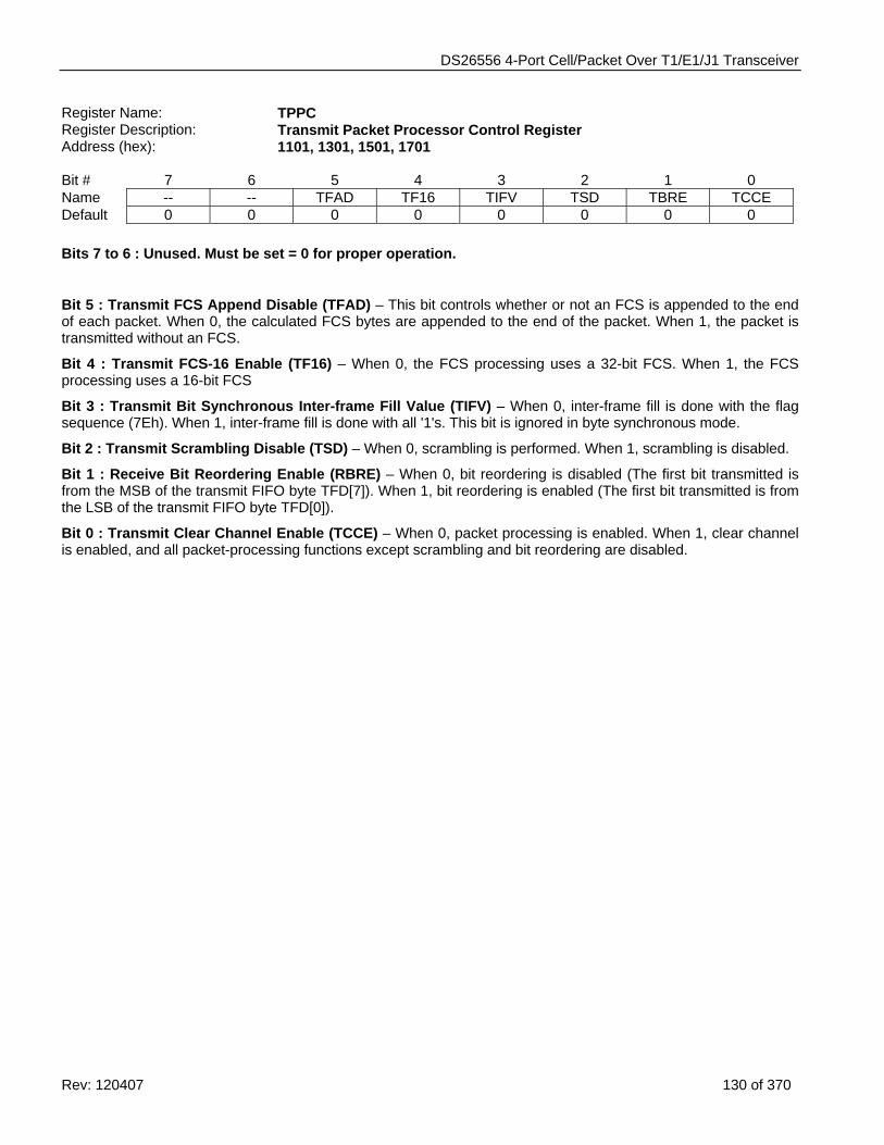
DS26556 4-Port Cell/Packet Over T1/E1/J1 Transceiver
Rev: 120407 130 of 370
Register Name: TPPC Register Description: Transmit Packet Processor Control Register Address (hex): 1101, 1301, 1501, 1701 Bit # 7 6 5 4 3 2 1 0 Name -- -- TFAD TF16 TIFV TSD TBRE TCCE Default 0 0 0 0 0 0 0 0 Bits 7 to 6 : Unused. Must be set = 0 for proper operation.
Bit 5 : Transmit FCS Append Disable (TFAD) – This bit controls whether or not an FCS is appended to the end of each packet. When 0, the calculated FCS bytes are appended to the end of the packet. When 1, the packet is transmitted without an FCS.
Bit 4 : Transmit FCS-16 Enable (TF16) – When 0, the FCS processing uses a 32-bit FCS. When 1, the FCS processing uses a 16-bit FCS
Bit 3 : Transmit Bit Synchronous Inter-frame Fill Value (TIFV) – When 0, inter-frame fill is done with the flag sequence (7Eh). When 1, inter-frame fill is done with all '1's. This bit is ignored in byte synchronous mode.
Bit 2 : Transmit Scrambling Disable (TSD) – When 0, scrambling is performed. When 1, scrambling is disabled.
Bit 1 : Receive Bit Reordering Enable (RBRE) – When 0, bit reordering is disabled (The first bit transmitted is from the MSB of the transmit FIFO byte TFD[7]). When 1, bit reordering is enabled (The first bit transmitted is from the LSB of the transmit FIFO byte TFD[0]).
Bit 0 : Transmit Clear Channel Enable (TCCE) – When 0, packet processing is enabled. When 1, clear channel is enabled, and all packet-processing functions except scrambling and bit reordering are disabled.
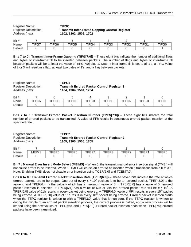
DS26556 4-Port Cell/Packet Over T1/E1/J1 Transceiver
Rev: 120407 131 of 370
Register Name: TIFGC Register Description: Transmit Inter-Frame Gapping Control Register Address (hex): 1102, 1302, 1502, 1702 Bit # 7 6 5 4 3 2 1 0 Name TIFG7 TIFG6 TIFG5 TIFG4 TIFG3 TIFG2 TIFG1 TIFG0 Default 0 0 0 0 0 0 0 1 Bits 7 to 0 : Transmit Inter-Frame Gapping (TIFG[7:0]) – These eight bits indicate the number of additional flags and bytes of inter-frame fill to be inserted between packets. The number of flags and bytes of inter-frame fill between packets will be at least the value of TIFG[7:0] plus 1. Note: If inter-frame fill is set to all 1’s, a TFIG value of 2 or 3 will result in a flag, at least two bytes of 1’s, and a flag between packets.
Register Name: TEPC1 Register Description: Transmit Errored Packet Control Register 1 Address (hex): 1104, 1304, 1504, 1704 Bit # 7 6 5 4 3 2 1 0 Name TPEN7 TPEN6 TPEN5 TPEN4 TPEN3 TPEN2 TPEN1 TPEN0 Default 0 0 0 0 0 0 0 0
Bits 7 to 0 : Transmit Errored Packet Insertion Number (TPEN[7:0]) – These eight bits indicate the total number of errored packets to be transmitted. A value of FFh results in continuous errored packet insertion at the specified rate. Register Name: TEPC2 Register Description: Transmit Errored Packet Control Register 2 Address (hex): 1105, 1305, 1505, 1705 Bit # 7 6 5 4 3 2 1 0 Name MEIMS TPER6 TPER5 TPER4 TPER3 TPER2 TPER1 TPER0 Default 0 0 0 0 0 0 0 0 Bit 7 : Manual Error Insert Mode Select (MEIMS) – When 0, the transmit manual error insertion signal (TMEI) will not cause errors to be inserted. When 1, TMEI will cause an error to be inserted when it transitions from a 0 to a 1. Note: Enabling TMEI does not disable error insertion using TCER[6:0] and TCEN[7:0].
Bits 6 to 0 : Transmit Errored Packet Insertion Rate (TPER[6:0]) – These seven bits indicate the rate at which errored packets are to be output. One out of every x * 10y packets is to be an errored packet. TPER[3:0] is the value x, and TPER[6:4] is the value y which has a maximum value of 6. If TPER[3:0] has a value of 0h errored packet insertion is disabled. If TPER[6:4] has a value of 6xh or 7xh the errored packet rate will be x * 106. A TPER[6:0] value of 01h results in every packet being errored. A TPER[6:0] value of 0Fh results in every 15th packet being errored. A TPER[6:0] value of 11h result in every 10th packet being errored. Errored packet insertion starts when the TEPC register is written to with a TPER[3:0] value that is non-zero. If the TEPC register is written to during the middle of an errored packet insertion process, the current process is halted, and a new process will be started using the new values of TPER[6:0] and TPEN[7:0}. Errored packet insertion ends when TPEN[7:0] errored packets have been transmitted.
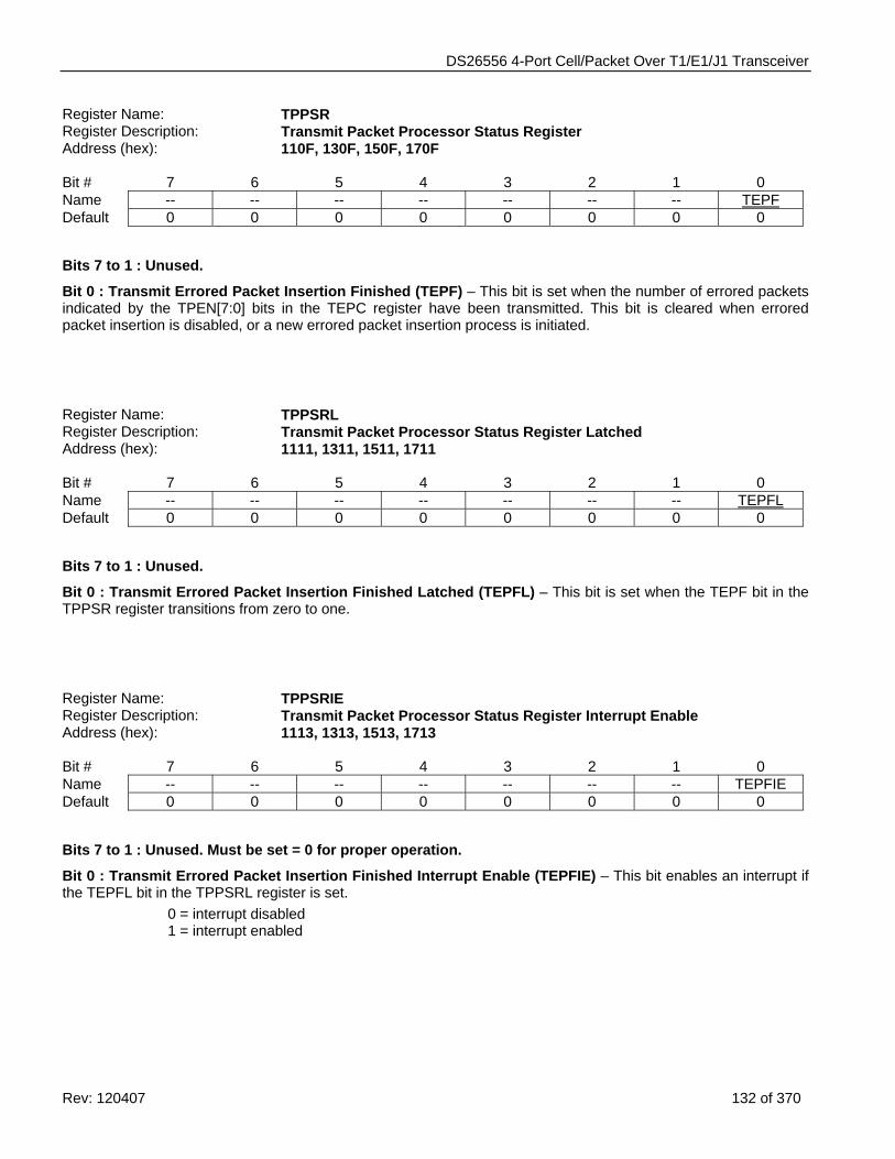
DS26556 4-Port Cell/Packet Over T1/E1/J1 Transceiver
Rev: 120407 132 of 370
Register Name: TPPSR Register Description: Transmit Packet Processor Status Register Address (hex): 110F, 130F, 150F, 170F Bit # 7 6 5 4 3 2 1 0 Name -- -- -- -- -- -- -- TEPF Default 0 0 0 0 0 0 0 0
Bits 7 to 1 : Unused.
Bit 0 : Transmit Errored Packet Insertion Finished (TEPF) – This bit is set when the number of errored packets indicated by the TPEN[7:0] bits in the TEPC register have been transmitted. This bit is cleared when errored packet insertion is disabled, or a new errored packet insertion process is initiated.
Register Name: TPPSRL Register Description: Transmit Packet Processor Status Register Latched Address (hex): 1111, 1311, 1511, 1711 Bit # 7 6 5 4 3 2 1 0 Name -- -- -- -- -- -- -- TEPFL Default 0 0 0 0 0 0 0 0
Bits 7 to 1 : Unused.
Bit 0 : Transmit Errored Packet Insertion Finished Latched (TEPFL) – This bit is set when the TEPF bit in the TPPSR register transitions from zero to one.
Register Name: TPPSRIE Register Description: Transmit Packet Processor Status Register Interrupt Enable Address (hex): 1113, 1313, 1513, 1713 Bit # 7 6 5 4 3 2 1 0 Name -- -- -- -- -- -- -- TEPFIE Default 0 0 0 0 0 0 0 0
Bits 7 to 1 : Unused. Must be set = 0 for proper operation.
Bit 0 : Transmit Errored Packet Insertion Finished Interrupt Enable (TEPFIE) – This bit enables an interrupt if the TEPFL bit in the TPPSRL register is set.
0 = interrupt disabled 1 = interrupt enabled
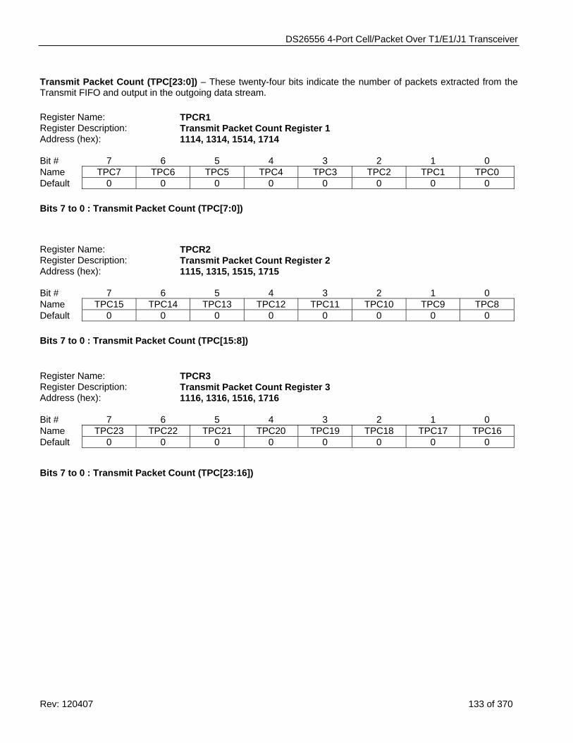
DS26556 4-Port Cell/Packet Over T1/E1/J1 Transceiver
Rev: 120407 133 of 370
Transmit Packet Count (TPC[23:0]) – These twenty-four bits indicate the number of packets extracted from the Transmit FIFO and output in the outgoing data stream. Register Name: TPCR1 Register Description: Transmit Packet Count Register 1 Address (hex): 1114, 1314, 1514, 1714 Bit # 7 6 5 4 3 2 1 0 Name TPC7 TPC6 TPC5 TPC4 TPC3 TPC2 TPC1 TPC0 Default 0 0 0 0 0 0 0 0 Bits 7 to 0 : Transmit Packet Count (TPC[7:0]) Register Name: TPCR2 Register Description: Transmit Packet Count Register 2 Address (hex): 1115, 1315, 1515, 1715 Bit # 7 6 5 4 3 2 1 0 Name TPC15 TPC14 TPC13 TPC12 TPC11 TPC10 TPC9 TPC8 Default 0 0 0 0 0 0 0 0 Bits 7 to 0 : Transmit Packet Count (TPC[15:8]) Register Name: TPCR3 Register Description: Transmit Packet Count Register 3 Address (hex): 1116, 1316, 1516, 1716 Bit # 7 6 5 4 3 2 1 0 Name TPC23 TPC22 TPC21 TPC20 TPC19 TPC18 TPC17 TPC16 Default 0 0 0 0 0 0 0 0
Bits 7 to 0 : Transmit Packet Count (TPC[23:16])
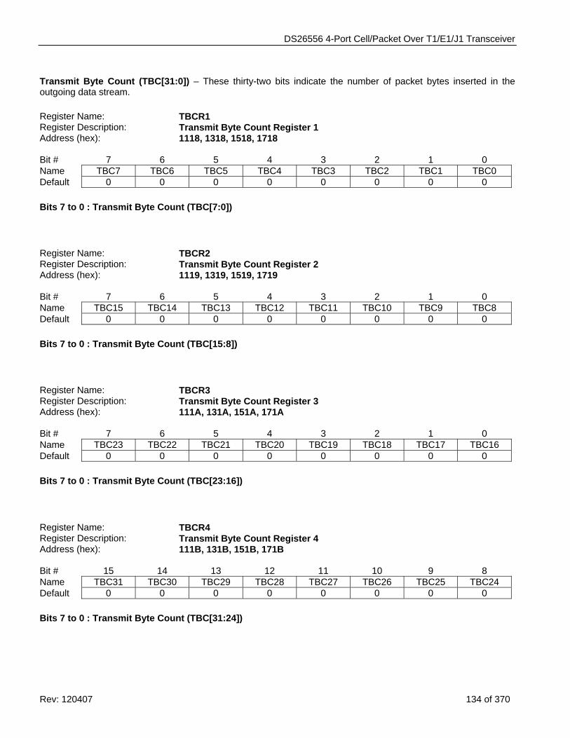
DS26556 4-Port Cell/Packet Over T1/E1/J1 Transceiver
Rev: 120407 134 of 370
Transmit Byte Count (TBC[31:0]) – These thirty-two bits indicate the number of packet bytes inserted in the outgoing data stream. Register Name: TBCR1 Register Description: Transmit Byte Count Register 1 Address (hex): 1118, 1318, 1518, 1718 Bit # 7 6 5 4 3 2 1 0 Name TBC7 TBC6 TBC5 TBC4 TBC3 TBC2 TBC1 TBC0 Default 0 0 0 0 0 0 0 0 Bits 7 to 0 : Transmit Byte Count (TBC[7:0])
Register Name: TBCR2 Register Description: Transmit Byte Count Register 2 Address (hex): 1119, 1319, 1519, 1719 Bit # 7 6 5 4 3 2 1 0 Name TBC15 TBC14 TBC13 TBC12 TBC11 TBC10 TBC9 TBC8 Default 0 0 0 0 0 0 0 0 Bits 7 to 0 : Transmit Byte Count (TBC[15:8])
Register Name: TBCR3 Register Description: Transmit Byte Count Register 3 Address (hex): 111A, 131A, 151A, 171A Bit # 7 6 5 4 3 2 1 0 Name TBC23 TBC22 TBC21 TBC20 TBC19 TBC18 TBC17 TBC16 Default 0 0 0 0 0 0 0 0 Bits 7 to 0 : Transmit Byte Count (TBC[23:16])
Register Name: TBCR4 Register Description: Transmit Byte Count Register 4 Address (hex): 111B, 131B, 151B, 171B Bit # 15 14 13 12 11 10 9 8 Name TBC31 TBC30 TBC29 TBC28 TBC27 TBC26 TBC25 TBC24 Default 0 0 0 0 0 0 0 0 Bits 7 to 0 : Transmit Byte Count (TBC[31:24])
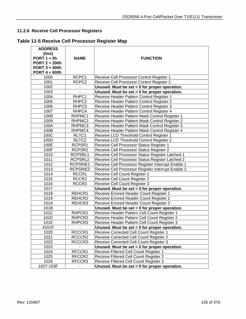
DS26556 4-Port Cell/Packet Over T1/E1/J1 Transceiver
Rev: 120407 135 of 370
11.2.6 Receive Cell Processor Registers
Table 11-5 Receive Cell Processor Register Map ADDRESS
(hex) PORT 1 + 0h PORT 2 + 200h PORT 3 + 400h PORT 4 + 600h
NAME
FUNCTION
1000 RCPC1 Receive Cell Processor Control Register 1 1001 RCPC2 Receive Cell Processor Control Register 2 1002 - Unused. Must be set = 0 for proper operation. 1003 - Unused. Must be set = 0 for proper operation. 1004 RHPC1 Receive Header Pattern Control Register 1 1005 RHPC2 Receive Header Pattern Control Register 2 1006 RHPC3 Receive Header Pattern Control Register 3 1007 RHPC4 Receive Header Pattern Control Register 4 1008 RHPMC1 Receive Header Pattern Mask Control Register 1 1009 RHPMC2 Receive Header Pattern Mask Control Register 2 100A RHPMC3 Receive Header Pattern Mask Control Register 3 100B RHPMC4 Receive Header Pattern Mask Control Register 4 100C RLTC1 Receive LCD Threshold Control Register 1 100D RLTC2 Receive LCD Threshold Control Register 2 100E RCPSR1 Receive Cell Processor Status Register 1 100F RCPSR2 Receive Cell Processor Status Register 2 1010 RCPSRL1 Receive Cell Processor Status Register Latched 1 1011 RCPSRL2 Receive Cell Processor Status Register Latched 2 1012 RCPSRIE1 Receive Cell Processor Register Interrupt Enable 1 1013 RCPSRIE2 Receive Cell Processor Register Interrupt Enable 2 1014 RCCR1 Receive Cell Count Register 1 1015 RCCR2 Receive Cell Count Register 2 1016 RCCR3 Receive Cell Count Register 3 1017 - Unused. Must be set = 0 for proper operation. 1018 REHCR1 Receive Errored Header Count Register 1 1019 REHCR2 Receive Errored Header Count Register 2 101A REHCR3 Receive Errored Header Count Register 3 101B - Unused. Must be set = 0 for proper operation. 101C RHPCR1 Receive Header Pattern Cell Count Register 1 101D RHPCR2 Receive Header Pattern Cell Count Register 2 101E RHPCR3 Receive Header Pattern Cell Count Register 3 4101F - Unused. Must be set = 0 for proper operation. 1020 RCCCR1 Receive Corrected Cell Count Register 1 1021 RCCCR2 Receive Corrected Cell Count Register 2 1022 RCCCR3 Receive Corrected Cell Count Register 3 1023 - Unused. Must be set = 0 for proper operation. 1024 RFCCR1 Receive Filtered Cell Count Register 1 1025 RFCCR2 Receive Filtered Cell Count Register 2 1026 RFCCR3 Receive Filtered Cell Count Register 3
1027-103F - Unused. Must be set = 0 for proper operation.
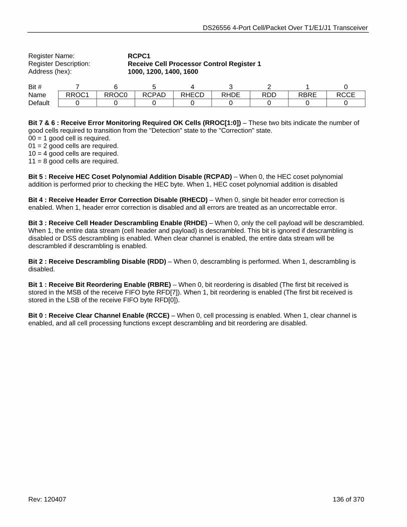
DS26556 4-Port Cell/Packet Over T1/E1/J1 Transceiver
Rev: 120407 136 of 370
Register Name: RCPC1 Register Description: Receive Cell Processor Control Register 1 Address (hex): 1000, 1200, 1400, 1600 Bit # 7 6 5 4 3 2 1 0 Name RROC1 RROC0 RCPAD RHECD RHDE RDD RBRE RCCE Default 0 0 0 0 0 0 0 0 Bit 7 & 6 : Receive Error Monitoring Required OK Cells (RROC[1:0]) – These two bits indicate the number of good cells required to transition from the "Detection" state to the "Correction" state. 00 = 1 good cell is required. 01 = 2 good cells are required. 10 = 4 good cells are required. 11 = 8 good cells are required. Bit 5 : Receive HEC Coset Polynomial Addition Disable (RCPAD) – When 0, the HEC coset polynomial addition is performed prior to checking the HEC byte. When 1, HEC coset polynomial addition is disabled Bit 4 : Receive Header Error Correction Disable (RHECD) – When 0, single bit header error correction is enabled. When 1, header error correction is disabled and all errors are treated as an uncorrectable error. Bit 3 : Receive Cell Header Descrambling Enable (RHDE) – When 0, only the cell payload will be descrambled. When 1, the entire data stream (cell header and payload) is descrambled. This bit is ignored if descrambling is disabled or DSS descrambling is enabled. When clear channel is enabled, the entire data stream will be descrambled if descrambling is enabled. Bit 2 : Receive Descrambling Disable (RDD) – When 0, descrambling is performed. When 1, descrambling is disabled. Bit 1 : Receive Bit Reordering Enable (RBRE) – When 0, bit reordering is disabled (The first bit received is stored in the MSB of the receive FIFO byte RFD[7]). When 1, bit reordering is enabled (The first bit received is stored in the LSB of the receive FIFO byte RFD[0]). Bit 0 : Receive Clear Channel Enable (RCCE) – When 0, cell processing is enabled. When 1, clear channel is enabled, and all cell processing functions except descrambling and bit reordering are disabled.
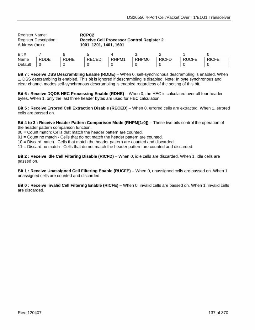
DS26556 4-Port Cell/Packet Over T1/E1/J1 Transceiver
Rev: 120407 137 of 370
Register Name: RCPC2 Register Description: Receive Cell Processor Control Register 2 Address (hex): 1001, 1201, 1401, 1601 Bit # 7 6 5 4 3 2 1 0 Name RDDE RDHE RECED RHPM1 RHPM0 RICFD RUCFE RICFE Default 0 0 0 0 0 0 0 0 Bit 7 : Receive DSS Descrambling Enable (RDDE) – When 0, self-synchronous descrambling is enabled. When 1, DSS descrambling is enabled. This bit is ignored if descrambling is disabled. Note: In byte synchronous and clear channel modes self-synchronous descrambling is enabled regardless of the setting of this bit. Bit 6 : Receive DQDB HEC Processing Enable (RDHE) – When 0, the HEC is calculated over all four header bytes. When 1, only the last three header bytes are used for HEC calculation. Bit 5 : Receive Errored Cell Extraction Disable (RECED) – When 0, errored cells are extracted. When 1, errored cells are passed on. Bit 4 to 3 : Receive Header Pattern Comparison Mode (RHPM[1:0]) – These two bits control the operation of the header pattern comparison function. 00 = Count match: Cells that match the header pattern are counted. 01 = Count no match - Cells that do not match the header pattern are counted. 10 = Discard match - Cells that match the header pattern are counted and discarded. 11 = Discard no match - Cells that do not match the header pattern are counted and discarded. Bit 2 : Receive Idle Cell Filtering Disable (RICFD) – When 0, idle cells are discarded. When 1, idle cells are passed on. Bit 1 : Receive Unassigned Cell Filtering Enable (RUCFE) – When 0, unassigned cells are passed on. When 1, unassigned cells are counted and discarded. Bit 0 : Receive Invalid Cell Filtering Enable (RICFE) – When 0, invalid cells are passed on. When 1, invalid cells are discarded.
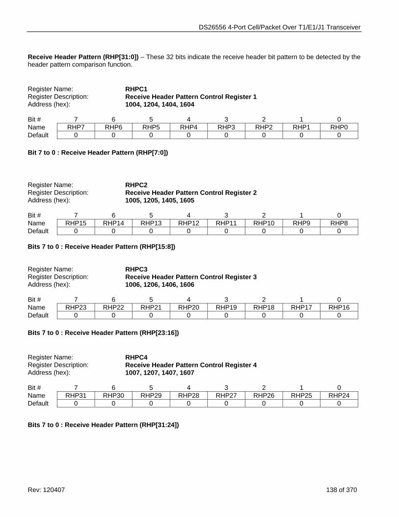
DS26556 4-Port Cell/Packet Over T1/E1/J1 Transceiver
Rev: 120407 138 of 370
Receive Header Pattern (RHP[31:0]) – These 32 bits indicate the receive header bit pattern to be detected by the header pattern comparison function. Register Name: RHPC1 Register Description: Receive Header Pattern Control Register 1 Address (hex): 1004, 1204, 1404, 1604 Bit # 7 6 5 4 3 2 1 0 Name RHP7 RHP6 RHP5 RHP4 RHP3 RHP2 RHP1 RHP0 Default 0 0 0 0 0 0 0 0 Bit 7 to 0 : Receive Header Pattern (RHP[7:0])
Register Name: RHPC2 Register Description: Receive Header Pattern Control Register 2 Address (hex): 1005, 1205, 1405, 1605 Bit # 7 6 5 4 3 2 1 0 Name RHP15 RHP14 RHP13 RHP12 RHP11 RHP10 RHP9 RHP8 Default 0 0 0 0 0 0 0 0 Bits 7 to 0 : Receive Header Pattern (RHP[15:8]) Register Name: RHPC3 Register Description: Receive Header Pattern Control Register 3 Address (hex): 1006, 1206, 1406, 1606 Bit # 7 6 5 4 3 2 1 0 Name RHP23 RHP22 RHP21 RHP20 RHP19 RHP18 RHP17 RHP16 Default 0 0 0 0 0 0 0 0 Bits 7 to 0 : Receive Header Pattern (RHP[23:16]) Register Name: RHPC4 Register Description: Receive Header Pattern Control Register 4 Address (hex): 1007, 1207, 1407, 1607 Bit # 7 6 5 4 3 2 1 0 Name RHP31 RHP30 RHP29 RHP28 RHP27 RHP26 RHP25 RHP24 Default 0 0 0 0 0 0 0 0
Bits 7 to 0 : Receive Header Pattern (RHP[31:24])
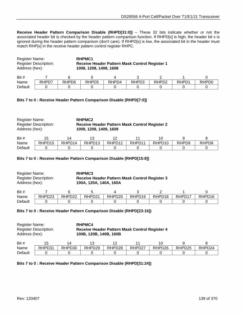
DS26556 4-Port Cell/Packet Over T1/E1/J1 Transceiver
Rev: 120407 139 of 370
Receive Header Pattern Comparison Disable (RHPD[31:0]) – These 32 bits indicate whether or not the associated header bit is checked by the header pattern comparison function. If RHPD[x] is high, the header bit x is ignored during the header pattern comparison (don't care). If RHPD[x] is low, the associated bit in the header must match RHP[x] in the receive header pattern control register RHPC.
Register Name: RHPMC1 Register Description: Receive Header Pattern Mask Control Register 1 Address (hex): 1008, 1208, 1408, 1608 Bit # 7 6 5 4 3 2 1 0 Name RHPD7 RHPD6 RHPD5 RHPD4 RHPD3 RHPD2 RHPD1 RHPD0 Default 0 0 0 0 0 0 0 0
Bits 7 to 0 : Receive Header Pattern Comparison Disable (RHPD[7:0])
Register Name: RHPMC2 Register Description: Receive Header Pattern Mask Control Register 2 Address (hex): 1009, 1209, 1409, 1609 Bit # 15 14 13 12 11 10 9 8 Name RHPD15 RHPD14 RHPD13 RHPD12 RHPD11 RHPD10 RHPD9 RHPD8 Default 0 0 0 0 0 0 0 0 Bits 7 to 0 : Receive Header Pattern Comparison Disable (RHPD[15:8]) Register Name: RHPMC3 Register Description: Receive Header Pattern Mask Control Register 3 Address (hex): 100A, 120A, 140A, 160A Bit # 7 6 5 4 3 2 1 0 Name RHPD23 RHPD22 RHPD21 RHPD20 RHPD19 RHPD18 RHPD17 RHPD16 Default 0 0 0 0 0 0 0 0 Bits 7 to 0 : Receive Header Pattern Comparison Disable (RHPD[23:16]) Register Name: RHPMC4 Register Description: Receive Header Pattern Mask Control Register 4 Address (hex): 100B, 120B, 140B, 160B Bit # 15 14 13 12 11 10 9 8 Name RHPD31 RHPD30 RHPD29 RHPD28 RHPD27 RHPD26 RHPD25 RHPD24 Default 0 0 0 0 0 0 0 0 Bits 7 to 0 : Receive Header Pattern Comparison Disable (RHPD[31:24])
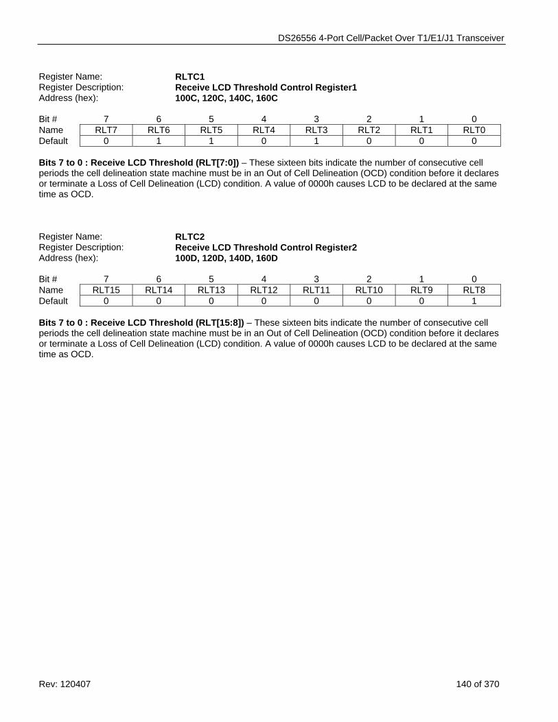
DS26556 4-Port Cell/Packet Over T1/E1/J1 Transceiver
Rev: 120407 140 of 370
Register Name: RLTC1 Register Description: Receive LCD Threshold Control Register1 Address (hex): 100C, 120C, 140C, 160C Bit # 7 6 5 4 3 2 1 0 Name RLT7 RLT6 RLT5 RLT4 RLT3 RLT2 RLT1 RLT0 Default 0 1 1 0 1 0 0 0 Bits 7 to 0 : Receive LCD Threshold (RLT[7:0]) – These sixteen bits indicate the number of consecutive cell periods the cell delineation state machine must be in an Out of Cell Delineation (OCD) condition before it declares or terminate a Loss of Cell Delineation (LCD) condition. A value of 0000h causes LCD to be declared at the same time as OCD.
Register Name: RLTC2 Register Description: Receive LCD Threshold Control Register2 Address (hex): 100D, 120D, 140D, 160D Bit # 7 6 5 4 3 2 1 0 Name RLT15 RLT14 RLT13 RLT12 RLT11 RLT10 RLT9 RLT8 Default 0 0 0 0 0 0 0 1 Bits 7 to 0 : Receive LCD Threshold (RLT[15:8]) – These sixteen bits indicate the number of consecutive cell periods the cell delineation state machine must be in an Out of Cell Delineation (OCD) condition before it declares or terminate a Loss of Cell Delineation (LCD) condition. A value of 0000h causes LCD to be declared at the same time as OCD.
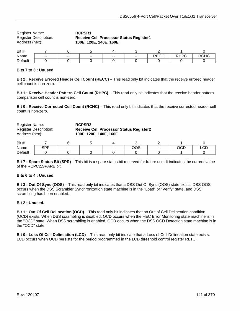
DS26556 4-Port Cell/Packet Over T1/E1/J1 Transceiver
Rev: 120407 141 of 370
Register Name: RCPSR1 Register Description: Receive Cell Processor Status Register1 Address (hex): 100E, 120E, 140E, 160E Bit # 7 6 5 4 3 2 1 0 Name -- -- -- -- -- RECC RHPC RCHC Default 0 0 0 0 0 0 0 0 Bits 7 to 3 : Unused. Bit 2 : Receive Errored Header Cell Count (RECC) – This read only bit indicates that the receive errored header cell count is non-zero. Bit 1 : Receive Header Pattern Cell Count (RHPC) – This read only bit indicates that the receive header pattern comparison cell count is non-zero. Bit 0 : Receive Corrected Cell Count (RCHC) – This read only bit indicates that the receive corrected header cell count is non-zero. Register Name: RCPSR2 Register Description: Receive Cell Processor Status Register2 Address (hex): 100F, 120F, 140F, 160F Bit # 7 6 5 4 3 2 1 0 Name SPR -- -- -- OOS -- OCD LCD Default 0 0 0 0 0 0 1 0 Bit 7 : Spare Status Bit (SPR) – This bit is a spare status bit reserved for future use. It indicates the current value of the RCPC2.SPARE bit. Bits 6 to 4 : Unused. Bit 3 : Out Of Sync (OOS) – This read only bit indicates that a DSS Out Of Sync (OOS) state exists. DSS OOS occurs when the DSS Scrambler Synchronization state machine is in the "Load" or "Verify" state, and DSS scrambling has been enabled. Bit 2 : Unused. Bit 1 : Out Of Cell Delineation (OCD) – This read only bit indicates that an Out of Cell Delineation condition (OCD) exists. When DSS scrambling is disabled, OCD occurs when the HEC Error Monitoring state machine is in the "OCD" state. When DSS scrambling is enabled, OCD occurs when the DSS OCD Detection state machine is in the "OCD" state. Bit 0 : Loss Of Cell Delineation (LCD) – This read only bit indicate that a Loss of Cell Delineation state exists. LCD occurs when OCD persists for the period programmed in the LCD threshold control register RLTC.
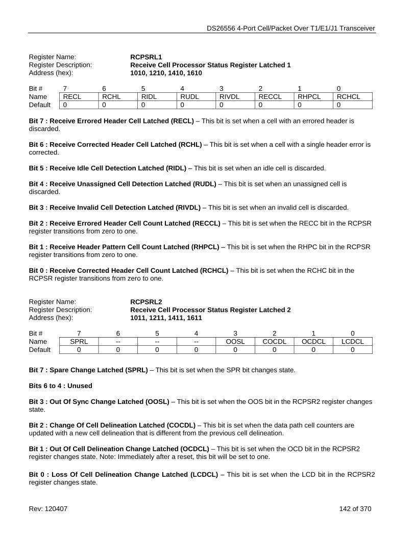
DS26556 4-Port Cell/Packet Over T1/E1/J1 Transceiver
Rev: 120407 142 of 370
Register Name: RCPSRL1 Register Description: Receive Cell Processor Status Register Latched 1 Address (hex): 1010, 1210, 1410, 1610 Bit # 7 6 5 4 3 2 1 0 Name RECL RCHL RIDL RUDL RIVDL RECCL RHPCL RCHCL Default 0 0 0 0 0 0 0 0 Bit 7 : Receive Errored Header Cell Latched (RECL) – This bit is set when a cell with an errored header is discarded. Bit 6 : Receive Corrected Header Cell Latched (RCHL) – This bit is set when a cell with a single header error is corrected. Bit 5 : Receive Idle Cell Detection Latched (RIDL) – This bit is set when an idle cell is discarded. Bit 4 : Receive Unassigned Cell Detection Latched (RUDL) – This bit is set when an unassigned cell is discarded. Bit 3 : Receive Invalid Cell Detection Latched (RIVDL) – This bit is set when an invalid cell is discarded. Bit 2 : Receive Errored Header Cell Count Latched (RECCL) – This bit is set when the RECC bit in the RCPSR register transitions from zero to one. Bit 1 : Receive Header Pattern Cell Count Latched (RHPCL) – This bit is set when the RHPC bit in the RCPSR register transitions from zero to one. Bit 0 : Receive Corrected Header Cell Count Latched (RCHCL) – This bit is set when the RCHC bit in the RCPSR register transitions from zero to one. Register Name: RCPSRL2 Register Description: Receive Cell Processor Status Register Latched 2 Address (hex): 1011, 1211, 1411, 1611 Bit # 7 6 5 4 3 2 1 0 Name SPRL -- -- -- OOSL COCDL OCDCL LCDCL Default 0 0 0 0 0 0 0 0 Bit 7 : Spare Change Latched (SPRL) – This bit is set when the SPR bit changes state. Bits 6 to 4 : Unused Bit 3 : Out Of Sync Change Latched (OOSL) – This bit is set when the OOS bit in the RCPSR2 register changes state. Bit 2 : Change Of Cell Delineation Latched (COCDL) – This bit is set when the data path cell counters are updated with a new cell delineation that is different from the previous cell delineation. Bit 1 : Out Of Cell Delineation Change Latched (OCDCL) – This bit is set when the OCD bit in the RCPSR2 register changes state. Note: Immediately after a reset, this bit will be set to one. Bit 0 : Loss Of Cell Delineation Change Latched (LCDCL) – This bit is set when the LCD bit in the RCPSR2 register changes state.
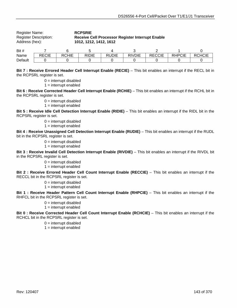
DS26556 4-Port Cell/Packet Over T1/E1/J1 Transceiver
Rev: 120407 143 of 370
Register Name: RCPSRIE Register Description: Receive Cell Processor Register Interrupt Enable Address (hex): 1012, 1212, 1412, 1612 Bit # 7 6 5 4 3 2 1 0 Name RECIE RCHIE RIDIE RUDIE RIVDIE RECCIE RHPCIE RCHCIE Default 0 0 0 0 0 0 0 0 Bit 7 : Receive Errored Header Cell Interrupt Enable (RECIE) – This bit enables an interrupt if the RECL bit in the RCPSRL register is set.
0 = interrupt disabled 1 = interrupt enabled
Bit 6 : Receive Corrected Header Cell Interrupt Enable (RCHIE) – This bit enables an interrupt if the RCHL bit in the RCPSRL register is set.
0 = interrupt disabled 1 = interrupt enabled
Bit 5 : Receive Idle Cell Detection Interrupt Enable (RIDIE) – This bit enables an interrupt if the RIDL bit in the RCPSRL register is set.
0 = interrupt disabled 1 = interrupt enabled
Bit 4 : Receive Unassigned Cell Detection Interrupt Enable (RUDIE) – This bit enables an interrupt if the RUDL bit in the RCPSRL register is set.
0 = interrupt disabled 1 = interrupt enabled
Bit 3 : Receive Invalid Cell Detection Interrupt Enable (RIVDIE) – This bit enables an interrupt if the RIVDL bit in the RCPSRL register is set.
0 = interrupt disabled 1 = interrupt enabled
Bit 2 : Receive Errored Header Cell Count Interrupt Enable (RECCIE) – This bit enables an interrupt if the RECCL bit in the RCPSRL register is set.
0 = interrupt disabled 1 = interrupt enabled
Bit 1 : Receive Header Pattern Cell Count Interrupt Enable (RHPCIE) – This bit enables an interrupt if the RHFCL bit in the RCPSRL register is set.
0 = interrupt disabled 1 = interrupt enabled
Bit 0 : Receive Corrected Header Cell Count Interrupt Enable (RCHCIE) – This bit enables an interrupt if the RCHCL bit in the RCPSRL register is set.
0 = interrupt disabled 1 = interrupt enabled
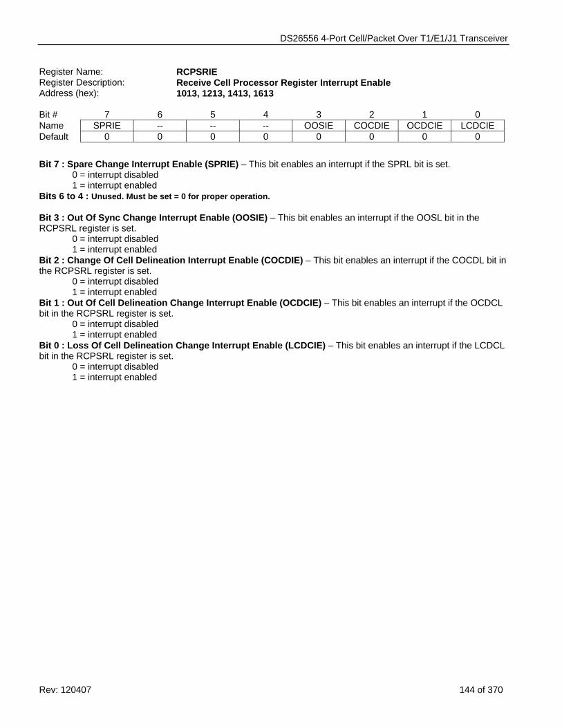
DS26556 4-Port Cell/Packet Over T1/E1/J1 Transceiver
Rev: 120407 144 of 370
Register Name: RCPSRIE Register Description: Receive Cell Processor Register Interrupt Enable Address (hex): 1013, 1213, 1413, 1613 Bit # 7 6 5 4 3 2 1 0 Name SPRIE -- -- -- OOSIE COCDIE OCDCIE LCDCIE Default 0 0 0 0 0 0 0 0 Bit 7 : Spare Change Interrupt Enable (SPRIE) – This bit enables an interrupt if the SPRL bit is set. 0 = interrupt disabled 1 = interrupt enabled Bits 6 to 4 : Unused. Must be set = 0 for proper operation. Bit 3 : Out Of Sync Change Interrupt Enable (OOSIE) – This bit enables an interrupt if the OOSL bit in the RCPSRL register is set. 0 = interrupt disabled 1 = interrupt enabled Bit 2 : Change Of Cell Delineation Interrupt Enable (COCDIE) – This bit enables an interrupt if the COCDL bit in the RCPSRL register is set. 0 = interrupt disabled 1 = interrupt enabled Bit 1 : Out Of Cell Delineation Change Interrupt Enable (OCDCIE) – This bit enables an interrupt if the OCDCL bit in the RCPSRL register is set. 0 = interrupt disabled 1 = interrupt enabled Bit 0 : Loss Of Cell Delineation Change Interrupt Enable (LCDCIE) – This bit enables an interrupt if the LCDCL bit in the RCPSRL register is set. 0 = interrupt disabled 1 = interrupt enabled
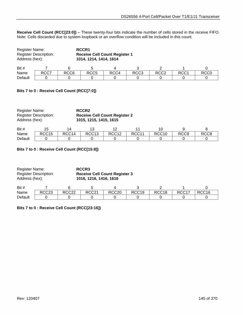
DS26556 4-Port Cell/Packet Over T1/E1/J1 Transceiver
Rev: 120407 145 of 370
Receive Cell Count (RCC[23:0]) – These twenty-four bits indicate the number of cells stored in the receive FIFO. Note: Cells discarded due to system loopback or an overflow condition will be included in this count.
Register Name: RCCR1 Register Description: Receive Cell Count Register 1 Address (hex): 1014, 1214, 1414, 1614 Bit # 7 6 5 4 3 2 1 0 Name RCC7 RCC6 RCC5 RCC4 RCC3 RCC2 RCC1 RCC0 Default 0 0 0 0 0 0 0 0
Bits 7 to 0 : Receive Cell Count (RCC[7:0])
Register Name: RCCR2 Register Description: Receive Cell Count Register 2 Address (hex): 1015, 1215, 1415, 1615 Bit # 15 14 13 12 11 10 9 8 Name RCC15 RCC14 RCC13 RCC12 RCC11 RCC10 RCC9 RCC8 Default 0 0 0 0 0 0 0 0 Bits 7 to 0 : Receive Cell Count (RCC[15:8])
Register Name: RCCR3 Register Description: Receive Cell Count Register 3 Address (hex): 1016, 1216, 1416, 1616 Bit # 7 6 5 4 3 2 1 0 Name RCC23 RCC22 RCC21 RCC20 RCC19 RCC18 RCC17 RCC16 Default 0 0 0 0 0 0 0 0 Bits 7 to 0 : Receive Cell Count (RCC[23:16])
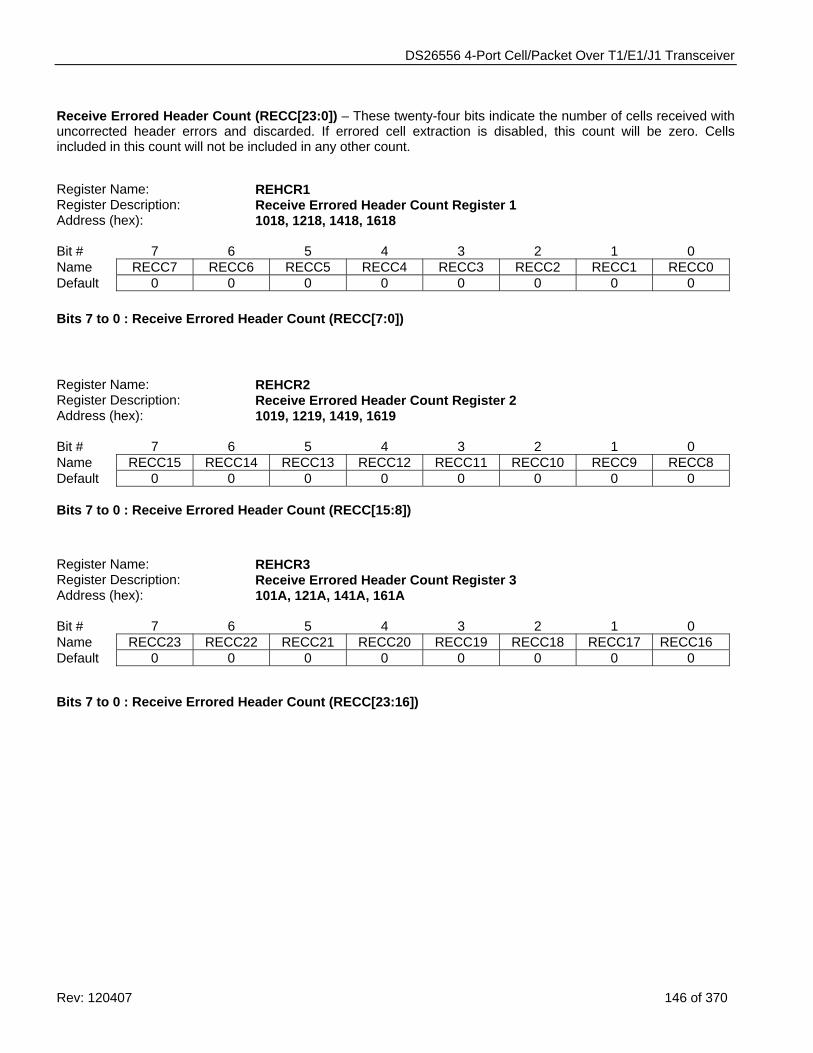
DS26556 4-Port Cell/Packet Over T1/E1/J1 Transceiver
Rev: 120407 146 of 370
Receive Errored Header Count (RECC[23:0]) – These twenty-four bits indicate the number of cells received with uncorrected header errors and discarded. If errored cell extraction is disabled, this count will be zero. Cells included in this count will not be included in any other count.
Register Name: REHCR1 Register Description: Receive Errored Header Count Register 1 Address (hex): 1018, 1218, 1418, 1618 Bit # 7 6 5 4 3 2 1 0 Name RECC7 RECC6 RECC5 RECC4 RECC3 RECC2 RECC1 RECC0 Default 0 0 0 0 0 0 0 0 Bits 7 to 0 : Receive Errored Header Count (RECC[7:0])
Register Name: REHCR2 Register Description: Receive Errored Header Count Register 2 Address (hex): 1019, 1219, 1419, 1619 Bit # 7 6 5 4 3 2 1 0 Name RECC15 RECC14 RECC13 RECC12 RECC11 RECC10 RECC9 RECC8 Default 0 0 0 0 0 0 0 0 Bits 7 to 0 : Receive Errored Header Count (RECC[15:8]) Register Name: REHCR3 Register Description: Receive Errored Header Count Register 3 Address (hex): 101A, 121A, 141A, 161A Bit # 7 6 5 4 3 2 1 0 Name RECC23 RECC22 RECC21 RECC20 RECC19 RECC18 RECC17 RECC16 Default 0 0 0 0 0 0 0 0
Bits 7 to 0 : Receive Errored Header Count (RECC[23:16])
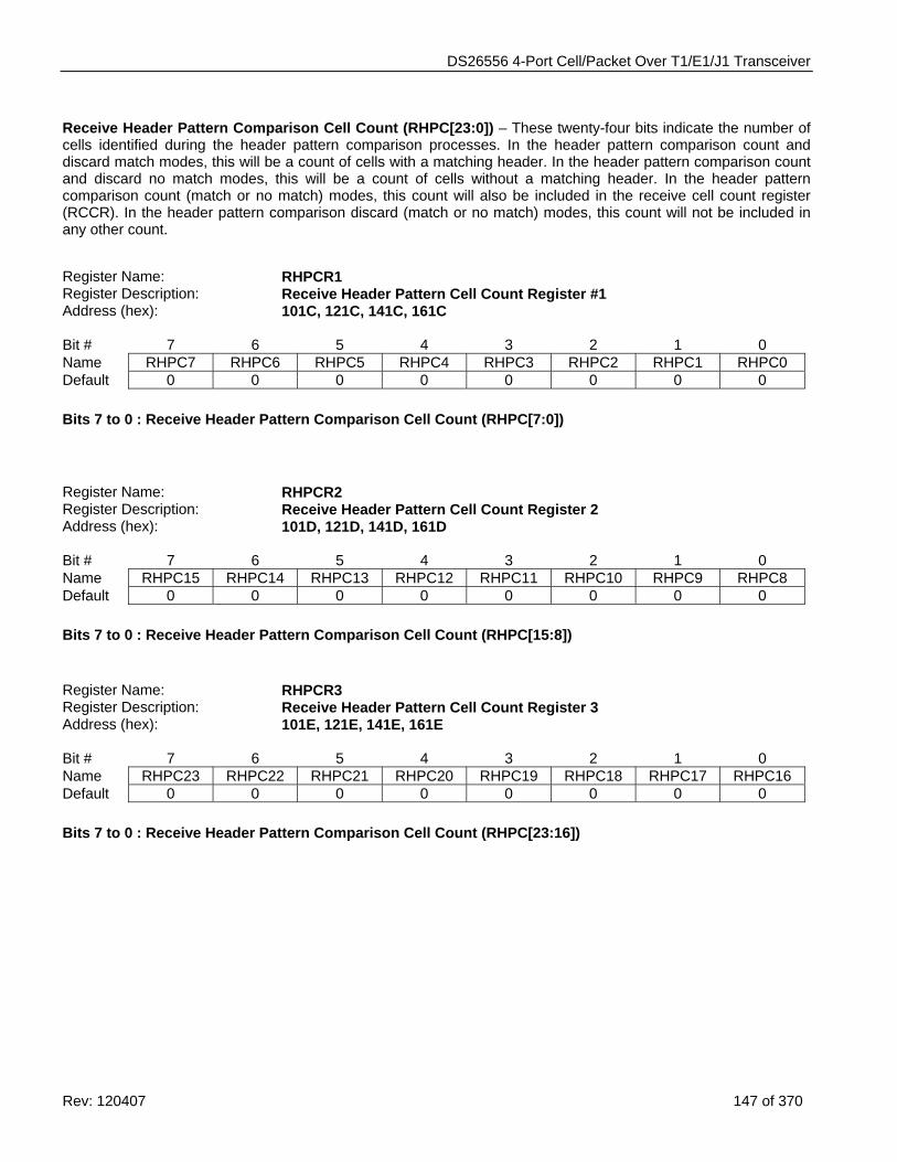
DS26556 4-Port Cell/Packet Over T1/E1/J1 Transceiver
Rev: 120407 147 of 370
Receive Header Pattern Comparison Cell Count (RHPC[23:0]) – These twenty-four bits indicate the number of cells identified during the header pattern comparison processes. In the header pattern comparison count and discard match modes, this will be a count of cells with a matching header. In the header pattern comparison count and discard no match modes, this will be a count of cells without a matching header. In the header pattern comparison count (match or no match) modes, this count will also be included in the receive cell count register (RCCR). In the header pattern comparison discard (match or no match) modes, this count will not be included in any other count.
Register Name: RHPCR1 Register Description: Receive Header Pattern Cell Count Register #1 Address (hex): 101C, 121C, 141C, 161C Bit # 7 6 5 4 3 2 1 0 Name RHPC7 RHPC6 RHPC5 RHPC4 RHPC3 RHPC2 RHPC1 RHPC0 Default 0 0 0 0 0 0 0 0 Bits 7 to 0 : Receive Header Pattern Comparison Cell Count (RHPC[7:0])
Register Name: RHPCR2 Register Description: Receive Header Pattern Cell Count Register 2 Address (hex): 101D, 121D, 141D, 161D Bit # 7 6 5 4 3 2 1 0 Name RHPC15 RHPC14 RHPC13 RHPC12 RHPC11 RHPC10 RHPC9 RHPC8 Default 0 0 0 0 0 0 0 0 Bits 7 to 0 : Receive Header Pattern Comparison Cell Count (RHPC[15:8]) Register Name: RHPCR3 Register Description: Receive Header Pattern Cell Count Register 3 Address (hex): 101E, 121E, 141E, 161E Bit # 7 6 5 4 3 2 1 0 Name RHPC23 RHPC22 RHPC21 RHPC20 RHPC19 RHPC18 RHPC17 RHPC16 Default 0 0 0 0 0 0 0 0 Bits 7 to 0 : Receive Header Pattern Comparison Cell Count (RHPC[23:16])
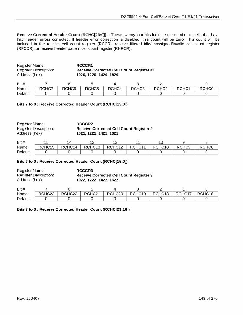
DS26556 4-Port Cell/Packet Over T1/E1/J1 Transceiver
Rev: 120407 148 of 370
Receive Corrected Header Count (RCHC[23:0]) – These twenty-four bits indicate the number of cells that have had header errors corrected. If header error correction is disabled, this count will be zero. This count will be included in the receive cell count register (RCCR), receive filtered idle/unassigned/invalid cell count register (RFCCR), or receive header pattern cell count register (RHPCR). Register Name: RCCCR1 Register Description: Receive Corrected Cell Count Register #1 Address (hex): 1020, 1220, 1420, 1620 Bit # 7 6 5 4 3 2 1 0 Name RCHC7 RCHC6 RCHC5 RCHC4 RCHC3 RCHC2 RCHC1 RCHC0 Default 0 0 0 0 0 0 0 0 Bits 7 to 0 : Receive Corrected Header Count (RCHC[15:0])
Register Name: RCCCR2 Register Description: Receive Corrected Cell Count Register 2 Address (hex): 1021, 1221, 1421, 1621 Bit # 15 14 13 12 11 10 9 8 Name RCHC15 RCHC14 RCHC13 RCHC12 RCHC11 RCHC10 RCHC9 RCHC8 Default 0 0 0 0 0 0 0 0 Bits 7 to 0 : Receive Corrected Header Count (RCHC[15:0]) Register Name: RCCCR3 Register Description: Receive Corrected Cell Count Register 3 Address (hex): 1022, 1222, 1422, 1622 Bit # 7 6 5 4 3 2 1 0 Name RCHC23 RCHC22 RCHC21 RCHC20 RCHC19 RCHC18 RCHC17 RCHC16 Default 0 0 0 0 0 0 0 0 Bits 7 to 0 : Receive Corrected Header Count (RCHC[23:16])
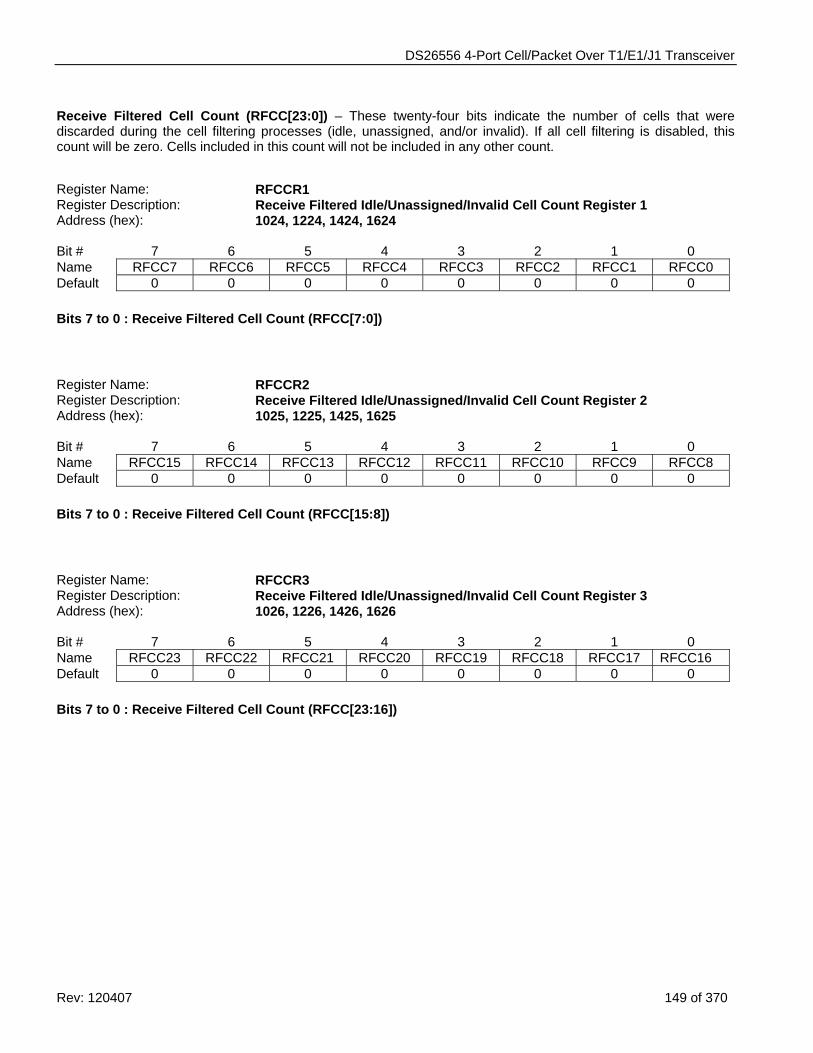
DS26556 4-Port Cell/Packet Over T1/E1/J1 Transceiver
Rev: 120407 149 of 370
Receive Filtered Cell Count (RFCC[23:0]) – These twenty-four bits indicate the number of cells that were discarded during the cell filtering processes (idle, unassigned, and/or invalid). If all cell filtering is disabled, this count will be zero. Cells included in this count will not be included in any other count.
Register Name: RFCCR1 Register Description: Receive Filtered Idle/Unassigned/Invalid Cell Count Register 1 Address (hex): 1024, 1224, 1424, 1624 Bit # 7 6 5 4 3 2 1 0 Name RFCC7 RFCC6 RFCC5 RFCC4 RFCC3 RFCC2 RFCC1 RFCC0 Default 0 0 0 0 0 0 0 0 Bits 7 to 0 : Receive Filtered Cell Count (RFCC[7:0])
Register Name: RFCCR2 Register Description: Receive Filtered Idle/Unassigned/Invalid Cell Count Register 2 Address (hex): 1025, 1225, 1425, 1625 Bit # 7 6 5 4 3 2 1 0 Name RFCC15 RFCC14 RFCC13 RFCC12 RFCC11 RFCC10 RFCC9 RFCC8 Default 0 0 0 0 0 0 0 0 Bits 7 to 0 : Receive Filtered Cell Count (RFCC[15:8])
Register Name: RFCCR3 Register Description: Receive Filtered Idle/Unassigned/Invalid Cell Count Register 3 Address (hex): 1026, 1226, 1426, 1626 Bit # 7 6 5 4 3 2 1 0 Name RFCC23 RFCC22 RFCC21 RFCC20 RFCC19 RFCC18 RFCC17 RFCC16 Default 0 0 0 0 0 0 0 0 Bits 7 to 0 : Receive Filtered Cell Count (RFCC[23:16])
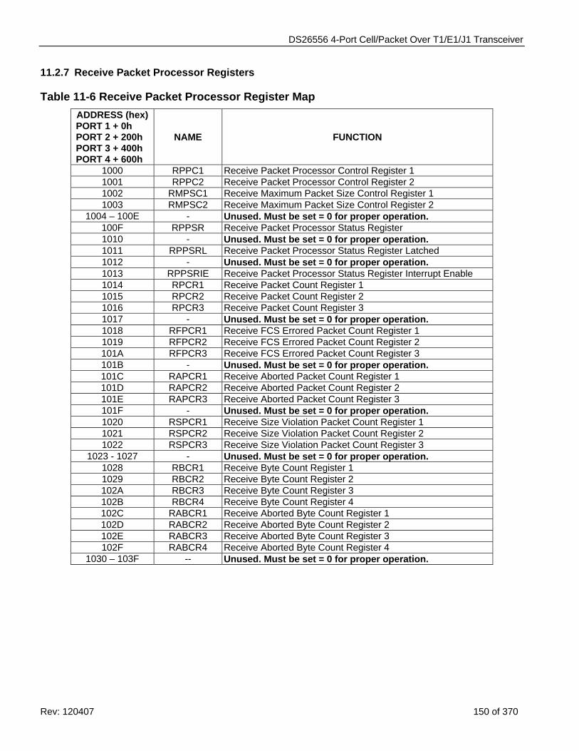
DS26556 4-Port Cell/Packet Over T1/E1/J1 Transceiver
Rev: 120407 150 of 370
11.2.7 Receive Packet Processor Registers
Table 11-6 Receive Packet Processor Register Map ADDRESS (hex) PORT 1 + 0h PORT 2 + 200h PORT 3 + 400h PORT 4 + 600h
NAME
FUNCTION
1000 RPPC1 Receive Packet Processor Control Register 1 1001 RPPC2 Receive Packet Processor Control Register 2 1002 RMPSC1 Receive Maximum Packet Size Control Register 1 1003 RMPSC2 Receive Maximum Packet Size Control Register 2
1004 – 100E - Unused. Must be set = 0 for proper operation. 100F RPPSR Receive Packet Processor Status Register 1010 - Unused. Must be set = 0 for proper operation. 1011 RPPSRL Receive Packet Processor Status Register Latched 1012 - Unused. Must be set = 0 for proper operation. 1013 RPPSRIE Receive Packet Processor Status Register Interrupt Enable 1014 RPCR1 Receive Packet Count Register 1 1015 RPCR2 Receive Packet Count Register 2 1016 RPCR3 Receive Packet Count Register 3 1017 - Unused. Must be set = 0 for proper operation. 1018 RFPCR1 Receive FCS Errored Packet Count Register 1 1019 RFPCR2 Receive FCS Errored Packet Count Register 2 101A RFPCR3 Receive FCS Errored Packet Count Register 3 101B - Unused. Must be set = 0 for proper operation. 101C RAPCR1 Receive Aborted Packet Count Register 1 101D RAPCR2 Receive Aborted Packet Count Register 2 101E RAPCR3 Receive Aborted Packet Count Register 3 101F - Unused. Must be set = 0 for proper operation. 1020 RSPCR1 Receive Size Violation Packet Count Register 1 1021 RSPCR2 Receive Size Violation Packet Count Register 2 1022 RSPCR3 Receive Size Violation Packet Count Register 3
1023 - 1027 - Unused. Must be set = 0 for proper operation. 1028 RBCR1 Receive Byte Count Register 1 1029 RBCR2 Receive Byte Count Register 2 102A RBCR3 Receive Byte Count Register 3 102B RBCR4 Receive Byte Count Register 4 102C RABCR1 Receive Aborted Byte Count Register 1 102D RABCR2 Receive Aborted Byte Count Register 2 102E RABCR3 Receive Aborted Byte Count Register 3 102F RABCR4 Receive Aborted Byte Count Register 4
1030 – 103F -- Unused. Must be set = 0 for proper operation.
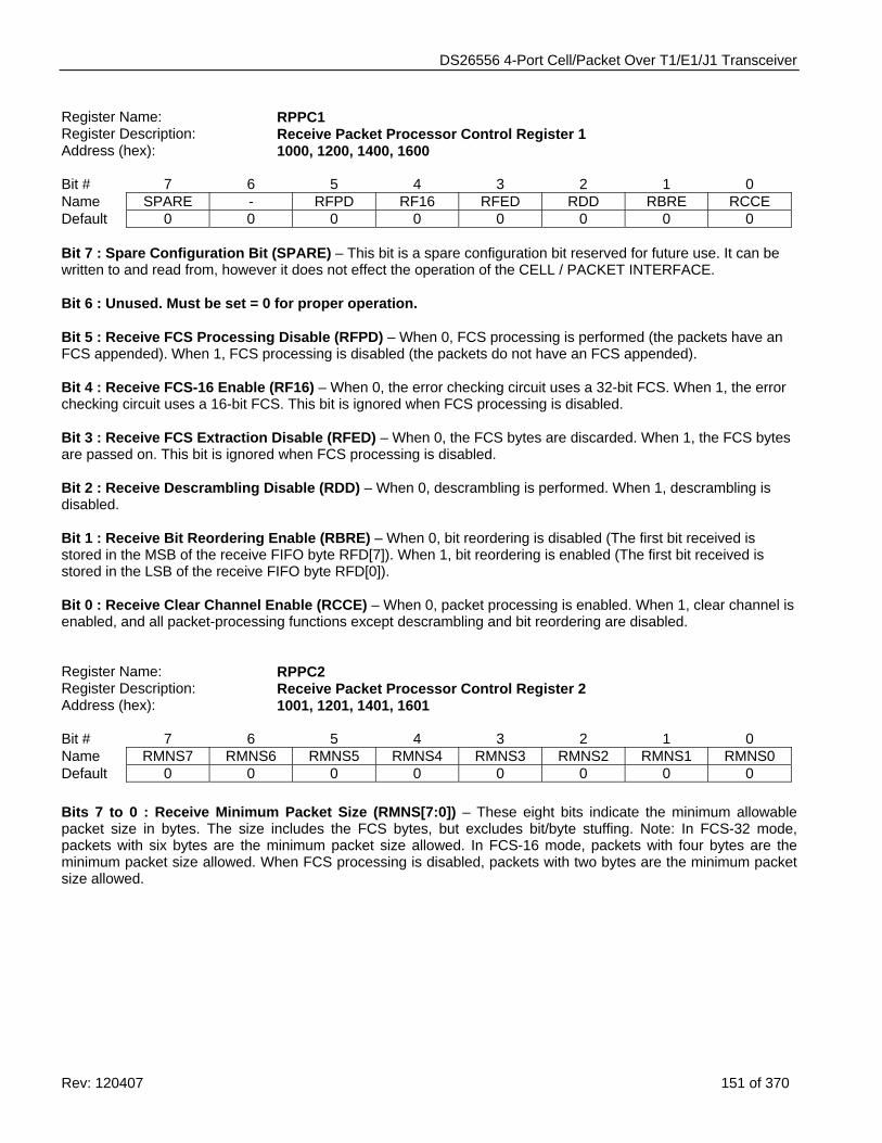
DS26556 4-Port Cell/Packet Over T1/E1/J1 Transceiver
Rev: 120407 151 of 370
Register Name: RPPC1 Register Description: Receive Packet Processor Control Register 1 Address (hex): 1000, 1200, 1400, 1600 Bit # 7 6 5 4 3 2 1 0 Name SPARE - RFPD RF16 RFED RDD RBRE RCCE Default 0 0 0 0 0 0 0 0 Bit 7 : Spare Configuration Bit (SPARE) – This bit is a spare configuration bit reserved for future use. It can be written to and read from, however it does not effect the operation of the CELL / PACKET INTERFACE. Bit 6 : Unused. Must be set = 0 for proper operation. Bit 5 : Receive FCS Processing Disable (RFPD) – When 0, FCS processing is performed (the packets have an FCS appended). When 1, FCS processing is disabled (the packets do not have an FCS appended). Bit 4 : Receive FCS-16 Enable (RF16) – When 0, the error checking circuit uses a 32-bit FCS. When 1, the error checking circuit uses a 16-bit FCS. This bit is ignored when FCS processing is disabled. Bit 3 : Receive FCS Extraction Disable (RFED) – When 0, the FCS bytes are discarded. When 1, the FCS bytes are passed on. This bit is ignored when FCS processing is disabled. Bit 2 : Receive Descrambling Disable (RDD) – When 0, descrambling is performed. When 1, descrambling is disabled. Bit 1 : Receive Bit Reordering Enable (RBRE) – When 0, bit reordering is disabled (The first bit received is stored in the MSB of the receive FIFO byte RFD[7]). When 1, bit reordering is enabled (The first bit received is stored in the LSB of the receive FIFO byte RFD[0]). Bit 0 : Receive Clear Channel Enable (RCCE) – When 0, packet processing is enabled. When 1, clear channel is enabled, and all packet-processing functions except descrambling and bit reordering are disabled. Register Name: RPPC2 Register Description: Receive Packet Processor Control Register 2 Address (hex): 1001, 1201, 1401, 1601 Bit # 7 6 5 4 3 2 1 0 Name RMNS7 RMNS6 RMNS5 RMNS4 RMNS3 RMNS2 RMNS1 RMNS0 Default 0 0 0 0 0 0 0 0 Bits 7 to 0 : Receive Minimum Packet Size (RMNS[7:0]) – These eight bits indicate the minimum allowable packet size in bytes. The size includes the FCS bytes, but excludes bit/byte stuffing. Note: In FCS-32 mode, packets with six bytes are the minimum packet size allowed. In FCS-16 mode, packets with four bytes are the minimum packet size allowed. When FCS processing is disabled, packets with two bytes are the minimum packet size allowed.
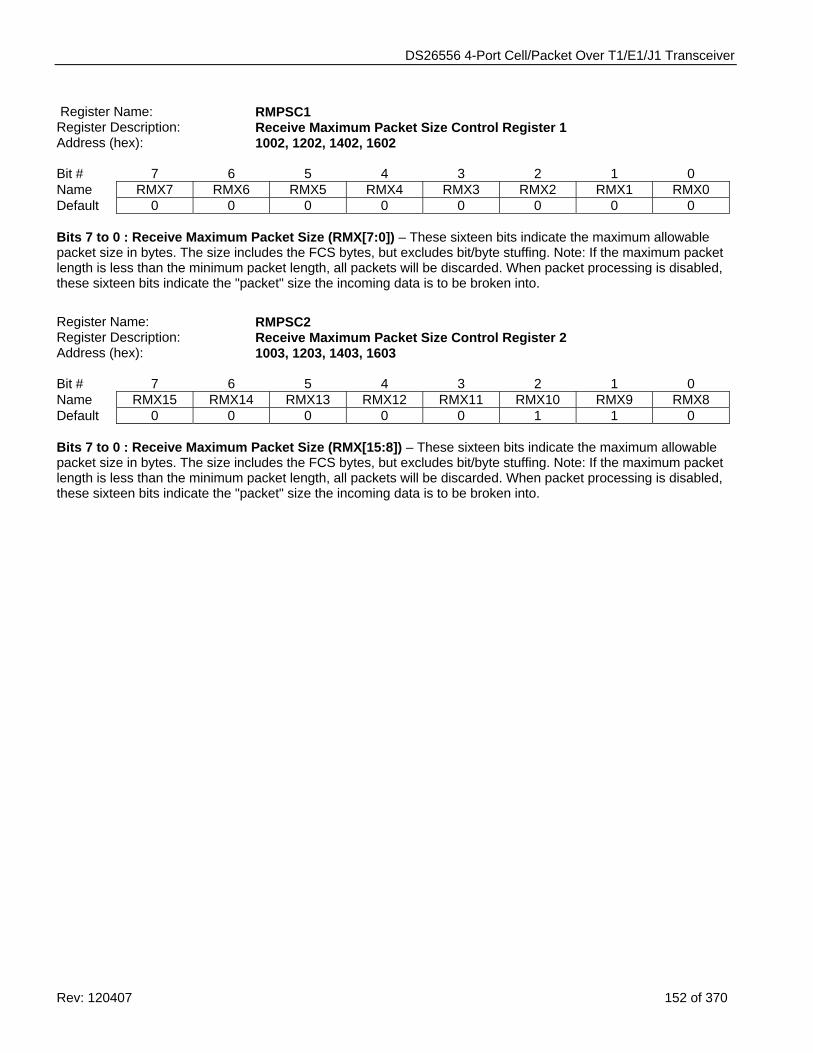
DS26556 4-Port Cell/Packet Over T1/E1/J1 Transceiver
Rev: 120407 152 of 370
Register Name: RMPSC1 Register Description: Receive Maximum Packet Size Control Register 1 Address (hex): 1002, 1202, 1402, 1602 Bit # 7 6 5 4 3 2 1 0 Name RMX7 RMX6 RMX5 RMX4 RMX3 RMX2 RMX1 RMX0 Default 0 0 0 0 0 0 0 0 Bits 7 to 0 : Receive Maximum Packet Size (RMX[7:0]) – These sixteen bits indicate the maximum allowable packet size in bytes. The size includes the FCS bytes, but excludes bit/byte stuffing. Note: If the maximum packet length is less than the minimum packet length, all packets will be discarded. When packet processing is disabled, these sixteen bits indicate the "packet" size the incoming data is to be broken into. Register Name: RMPSC2 Register Description: Receive Maximum Packet Size Control Register 2 Address (hex): 1003, 1203, 1403, 1603 Bit # 7 6 5 4 3 2 1 0 Name RMX15 RMX14 RMX13 RMX12 RMX11 RMX10 RMX9 RMX8 Default 0 0 0 0 0 1 1 0 Bits 7 to 0 : Receive Maximum Packet Size (RMX[15:8]) – These sixteen bits indicate the maximum allowable packet size in bytes. The size includes the FCS bytes, but excludes bit/byte stuffing. Note: If the maximum packet length is less than the minimum packet length, all packets will be discarded. When packet processing is disabled, these sixteen bits indicate the "packet" size the incoming data is to be broken into.
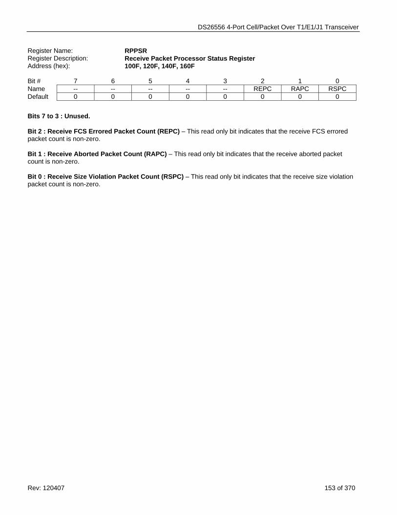
DS26556 4-Port Cell/Packet Over T1/E1/J1 Transceiver
Rev: 120407 153 of 370
Register Name: RPPSR Register Description: Receive Packet Processor Status Register Address (hex): 100F, 120F, 140F, 160F Bit # 7 6 5 4 3 2 1 0 Name -- -- -- -- -- REPC RAPC RSPC Default 0 0 0 0 0 0 0 0 Bits 7 to 3 : Unused. Bit 2 : Receive FCS Errored Packet Count (REPC) – This read only bit indicates that the receive FCS errored packet count is non-zero. Bit 1 : Receive Aborted Packet Count (RAPC) – This read only bit indicates that the receive aborted packet count is non-zero. Bit 0 : Receive Size Violation Packet Count (RSPC) – This read only bit indicates that the receive size violation packet count is non-zero.
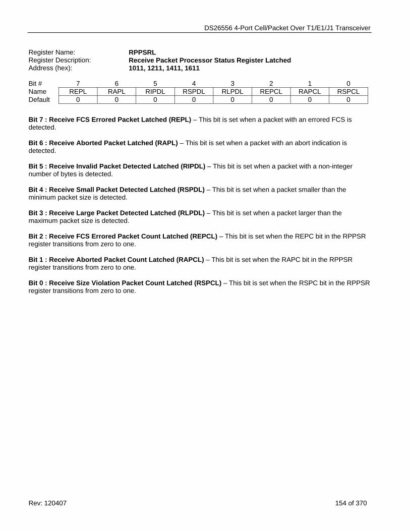
DS26556 4-Port Cell/Packet Over T1/E1/J1 Transceiver
Rev: 120407 154 of 370
Register Name: RPPSRL Register Description: Receive Packet Processor Status Register Latched Address (hex): 1011, 1211, 1411, 1611 Bit # 7 6 5 4 3 2 1 0 Name REPL RAPL RIPDL RSPDL RLPDL REPCL RAPCL RSPCL Default 0 0 0 0 0 0 0 0 Bit 7 : Receive FCS Errored Packet Latched (REPL) – This bit is set when a packet with an errored FCS is detected. Bit 6 : Receive Aborted Packet Latched (RAPL) – This bit is set when a packet with an abort indication is detected. Bit 5 : Receive Invalid Packet Detected Latched (RIPDL) – This bit is set when a packet with a non-integer number of bytes is detected. Bit 4 : Receive Small Packet Detected Latched (RSPDL) – This bit is set when a packet smaller than the minimum packet size is detected. Bit 3 : Receive Large Packet Detected Latched (RLPDL) – This bit is set when a packet larger than the maximum packet size is detected. Bit 2 : Receive FCS Errored Packet Count Latched (REPCL) – This bit is set when the REPC bit in the RPPSR register transitions from zero to one. Bit 1 : Receive Aborted Packet Count Latched (RAPCL) – This bit is set when the RAPC bit in the RPPSR register transitions from zero to one. Bit 0 : Receive Size Violation Packet Count Latched (RSPCL) – This bit is set when the RSPC bit in the RPPSR register transitions from zero to one.
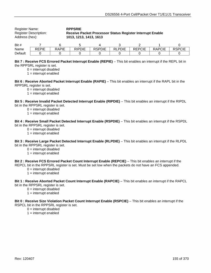
DS26556 4-Port Cell/Packet Over T1/E1/J1 Transceiver
Rev: 120407 155 of 370
Register Name: RPPSRIE Register Description: Receive Packet Processor Status Register Interrupt Enable Address (hex): 1013, 1213, 1413, 1613 Bit # 7 6 5 4 3 2 1 0 Name REPIE RAPIE RIPDIE RSPDIE RLPDIE REPCIE RAPCIE RSPCIE Default 0 0 0 0 0 0 0 0 Bit 7 : Receive FCS Errored Packet Interrupt Enable (REPIE) – This bit enables an interrupt if the REPL bit in the RPPSRL register is set. 0 = interrupt disabled 1 = interrupt enabled Bit 6 : Receive Aborted Packet Interrupt Enable (RAPIE) – This bit enables an interrupt if the RAPL bit in the RPPSRL register is set. 0 = interrupt disabled 1 = interrupt enabled Bit 5 : Receive Invalid Packet Detected Interrupt Enable (RIPDIE) – This bit enables an interrupt if the RIPDL bit in the RPPSRL register is set. 0 = interrupt disabled 1 = interrupt enabled Bit 4 : Receive Small Packet Detected Interrupt Enable (RSPDIE) – This bit enables an interrupt if the RSPDL bit in the RPPSRL register is set. 0 = interrupt disabled 1 = interrupt enabled Bit 3 : Receive Large Packet Detected Interrupt Enable (RLPDIE) – This bit enables an interrupt if the RLPDL bit in the RPPSRL register is set. 0 = interrupt disabled 1 = interrupt enabled Bit 2 : Receive FCS Errored Packet Count Interrupt Enable (REPCIE) – This bit enables an interrupt if the REPCL bit in the RPPSRL register is set. Must be set low when the packets do not have an FCS appended. 0 = interrupt disabled 1 = interrupt enabled Bit 1 : Receive Aborted Packet Count Interrupt Enable (RAPCIE) – This bit enables an interrupt if the RAPCL bit in the RPPSRL register is set. 0 = interrupt disabled 1 = interrupt enabled Bit 0 : Receive Size Violation Packet Count Interrupt Enable (RSPCIE) – This bit enables an interrupt if the RSPCL bit in the RPPSRL register is set. 0 = interrupt disabled 1 = interrupt enabled
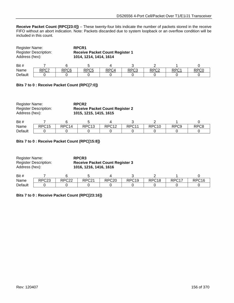
DS26556 4-Port Cell/Packet Over T1/E1/J1 Transceiver
Rev: 120407 156 of 370
Receive Packet Count (RPC[23:0]) – These twenty-four bits indicate the number of packets stored in the receive FIFO without an abort indication. Note: Packets discarded due to system loopback or an overflow condition will be included in this count.
Register Name: RPCR1 Register Description: Receive Packet Count Register 1 Address (hex): 1014, 1214, 1414, 1614 Bit # 7 6 5 4 3 2 1 0 Name RPC7 RPC6 RPC5 RPC4 RPC3 RPC2 RPC1 RPC0 Default 0 0 0 0 0 0 0 0 Bits 7 to 0 : Receive Packet Count (RPC[7:0])
Register Name: RPCR2 Register Description: Receive Packet Count Register 2 Address (hex): 1015, 1215, 1415, 1615 Bit # 7 6 5 4 3 2 1 0 Name RPC15 RPC14 RPC13 RPC12 RPC11 RPC10 RPC9 RPC8 Default 0 0 0 0 0 0 0 0 Bits 7 to 0 : Receive Packet Count (RPC[15:8])
Register Name: RPCR3 Register Description: Receive Packet Count Register 3 Address (hex): 1016, 1216, 1416, 1616 Bit # 7 6 5 4 3 2 1 0 Name RPC23 RPC22 RPC21 RPC20 RPC19 RPC18 RPC17 RPC16 Default 0 0 0 0 0 0 0 0 Bits 7 to 0 : Receive Packet Count (RPC[23:16])
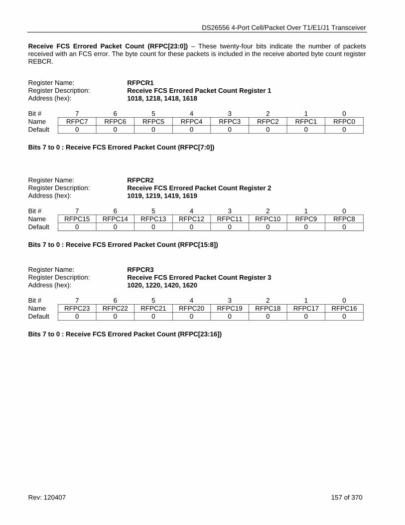
DS26556 4-Port Cell/Packet Over T1/E1/J1 Transceiver
Rev: 120407 157 of 370
Receive FCS Errored Packet Count (RFPC[23:0]) – These twenty-four bits indicate the number of packets received with an FCS error. The byte count for these packets is included in the receive aborted byte count register REBCR.
Register Name: RFPCR1 Register Description: Receive FCS Errored Packet Count Register 1 Address (hex): 1018, 1218, 1418, 1618 Bit # 7 6 5 4 3 2 1 0 Name RFPC7 RFPC6 RFPC5 RFPC4 RFPC3 RFPC2 RFPC1 RFPC0 Default 0 0 0 0 0 0 0 0 Bits 7 to 0 : Receive FCS Errored Packet Count (RFPC[7:0])
Register Name: RFPCR2 Register Description: Receive FCS Errored Packet Count Register 2 Address (hex): 1019, 1219, 1419, 1619 Bit # 7 6 5 4 3 2 1 0 Name RFPC15 RFPC14 RFPC13 RFPC12 RFPC11 RFPC10 RFPC9 RFPC8 Default 0 0 0 0 0 0 0 0 Bits 7 to 0 : Receive FCS Errored Packet Count (RFPC[15:8]) Register Name: RFPCR3 Register Description: Receive FCS Errored Packet Count Register 3 Address (hex): 1020, 1220, 1420, 1620 Bit # 7 6 5 4 3 2 1 0 Name RFPC23 RFPC22 RFPC21 RFPC20 RFPC19 RFPC18 RFPC17 RFPC16 Default 0 0 0 0 0 0 0 0 Bits 7 to 0 : Receive FCS Errored Packet Count (RFPC[23:16])
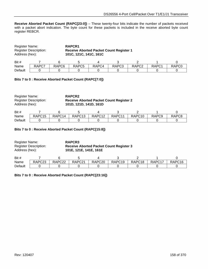
DS26556 4-Port Cell/Packet Over T1/E1/J1 Transceiver
Rev: 120407 158 of 370
Receive Aborted Packet Count (RAPC[23:0]) – These twenty-four bits indicate the number of packets received with a packet abort indication. The byte count for these packets is included in the receive aborted byte count register REBCR.
Register Name: RAPCR1 Register Description: Receive Aborted Packet Count Register 1 Address (hex): 101C, 121C, 141C, 161C Bit # 7 6 5 4 3 2 1 0 Name RAPC7 RAPC6 RAPC5 RAPC4 RAPC3 RAPC2 RAPC1 RAPC0 Default 0 0 0 0 0 0 0 0 Bits 7 to 0 : Receive Aborted Packet Count (RAPC[7:0])
Register Name: RAPCR2 Register Description: Receive Aborted Packet Count Register 2 Address (hex): 101D, 121D, 141D, 161D Bit # 7 6 5 4 3 2 1 0 Name RAPC15 RAPC14 RAPC13 RAPC12 RAPC11 RAPC10 RAPC9 RAPC8 Default 0 0 0 0 0 0 0 0 Bits 7 to 0 : Receive Aborted Packet Count (RAPC[15:8]) Register Name: RAPCR3 Register Description: Receive Aborted Packet Count Register 3 Address (hex): 101E, 121E, 141E, 161E Bit # 7 6 5 4 3 2 1 0 Name RAPC23 RAPC22 RAPC21 RAPC20 RAPC19 RAPC18 RAPC17 RAPC16 Default 0 0 0 0 0 0 0 0 Bits 7 to 0 : Receive Aborted Packet Count (RAPC[23:16])
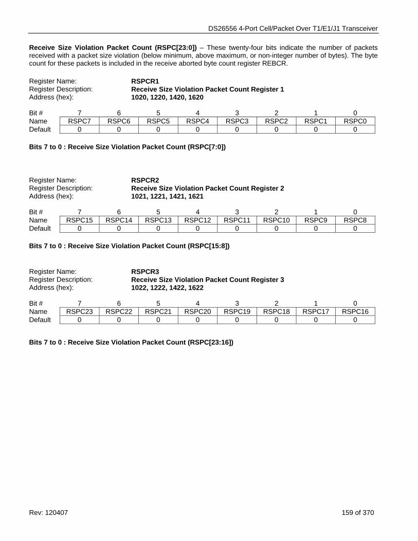
DS26556 4-Port Cell/Packet Over T1/E1/J1 Transceiver
Rev: 120407 159 of 370
Receive Size Violation Packet Count (RSPC[23:0]) – These twenty-four bits indicate the number of packets received with a packet size violation (below minimum, above maximum, or non-integer number of bytes). The byte count for these packets is included in the receive aborted byte count register REBCR. Register Name: RSPCR1 Register Description: Receive Size Violation Packet Count Register 1 Address (hex): 1020, 1220, 1420, 1620 Bit # 7 6 5 4 3 2 1 0 Name RSPC7 RSPC6 RSPC5 RSPC4 RSPC3 RSPC2 RSPC1 RSPC0 Default 0 0 0 0 0 0 0 0 Bits 7 to 0 : Receive Size Violation Packet Count (RSPC[7:0])
Register Name: RSPCR2 Register Description: Receive Size Violation Packet Count Register 2 Address (hex): 1021, 1221, 1421, 1621 Bit # 7 6 5 4 3 2 1 0 Name RSPC15 RSPC14 RSPC13 RSPC12 RSPC11 RSPC10 RSPC9 RSPC8 Default 0 0 0 0 0 0 0 0 Bits 7 to 0 : Receive Size Violation Packet Count (RSPC[15:8]) Register Name: RSPCR3 Register Description: Receive Size Violation Packet Count Register 3 Address (hex): 1022, 1222, 1422, 1622 Bit # 7 6 5 4 3 2 1 0 Name RSPC23 RSPC22 RSPC21 RSPC20 RSPC19 RSPC18 RSPC17 RSPC16 Default 0 0 0 0 0 0 0 0
Bits 7 to 0 : Receive Size Violation Packet Count (RSPC[23:16])
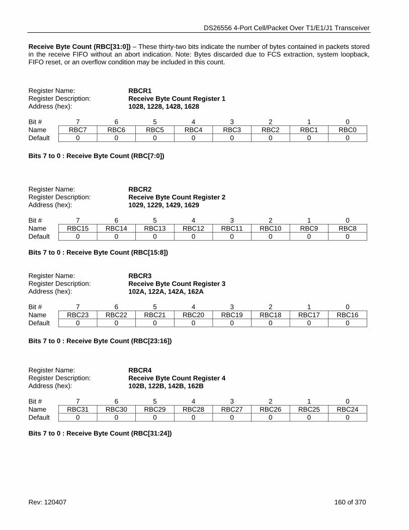
DS26556 4-Port Cell/Packet Over T1/E1/J1 Transceiver
Rev: 120407 160 of 370
Receive Byte Count (RBC[31:0]) – These thirty-two bits indicate the number of bytes contained in packets stored in the receive FIFO without an abort indication. Note: Bytes discarded due to FCS extraction, system loopback, FIFO reset, or an overflow condition may be included in this count.
Register Name: RBCR1 Register Description: Receive Byte Count Register 1 Address (hex): 1028, 1228, 1428, 1628 Bit # 7 6 5 4 3 2 1 0 Name RBC7 RBC6 RBC5 RBC4 RBC3 RBC2 RBC1 RBC0 Default 0 0 0 0 0 0 0 0 Bits 7 to 0 : Receive Byte Count (RBC[7:0])
Register Name: RBCR2 Register Description: Receive Byte Count Register 2 Address (hex): 1029, 1229, 1429, 1629 Bit # 7 6 5 4 3 2 1 0 Name RBC15 RBC14 RBC13 RBC12 RBC11 RBC10 RBC9 RBC8 Default 0 0 0 0 0 0 0 0 Bits 7 to 0 : Receive Byte Count (RBC[15:8]) Register Name: RBCR3 Register Description: Receive Byte Count Register 3 Address (hex): 102A, 122A, 142A, 162A Bit # 7 6 5 4 3 2 1 0 Name RBC23 RBC22 RBC21 RBC20 RBC19 RBC18 RBC17 RBC16 Default 0 0 0 0 0 0 0 0 Bits 7 to 0 : Receive Byte Count (RBC[23:16])
Register Name: RBCR4 Register Description: Receive Byte Count Register 4 Address (hex): 102B, 122B, 142B, 162B Bit # 7 6 5 4 3 2 1 0 Name RBC31 RBC30 RBC29 RBC28 RBC27 RBC26 RBC25 RBC24 Default 0 0 0 0 0 0 0 0 Bits 7 to 0 : Receive Byte Count (RBC[31:24])
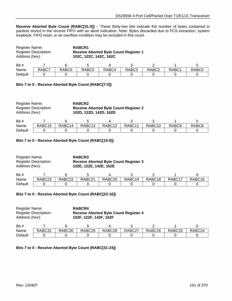
DS26556 4-Port Cell/Packet Over T1/E1/J1 Transceiver
Rev: 120407 161 of 370
Receive Aborted Byte Count (RABC[31:0]) – These thirty-two bits indicate the number of bytes contained in packets stored in the receive FIFO with an abort indication. Note: Bytes discarded due to FCS extraction, system loopback, FIFO reset, or an overflow condition may be included in this count.
Register Name: RABCR1 Register Description: Receive Aborted Byte Count Register 1 Address (hex): 102C, 122C, 142C, 162C Bit # 7 6 5 4 3 2 1 0 Name RABC7 RABC6 RABC5 RABC4 RABC3 RABC2 RABC1 RABC0 Default 0 0 0 0 0 0 0 0 Bits 7 to 0 : Receive Aborted Byte Count (RABC[7:0])
Register Name: RABCR2 Register Description: Receive Aborted Byte Count Register 2 Address (hex): 102D, 122D, 142D, 162D Bit # 7 6 5 4 3 2 1 0 Name RABC15 RABC14 RABC13 RABC12 RABC11 RABC10 RABC9 RABC8 Default 0 0 0 0 0 0 0 0 Bits 7 to 0 : Receive Aborted Byte Count (RABC[15:8])
Register Name: RABCR3 Register Description: Receive Aborted Byte Count Register 3 Address (hex): 102E, 122E, 142E, 162E Bit # 7 6 5 4 3 2 1 0 Name RABC23 RABC22 RABC21 RABC20 RABC19 RABC18 RABC17 RABC16 Default 0 0 0 0 0 0 0 0 Bits 7 to 0 : Receive Aborted Byte Count (RABC[23:16]) Register Name: RABCR4 Register Description: Receive Aborted Byte Count Register 4 Address (hex): 102F, 122F, 142F, 162F Bit # 7 6 5 4 3 2 1 0 Name RABC31 RABC30 RABC29 RABC28 RABC27 RABC26 RABC25 RABC24 Default 0 0 0 0 0 0 0 0
Bits 7 to 0 : Receive Aborted Byte Count (RABC[31:24])
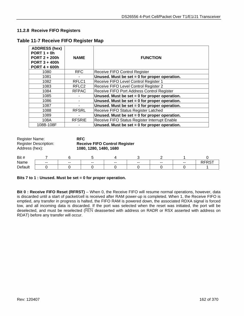
DS26556 4-Port Cell/Packet Over T1/E1/J1 Transceiver
Rev: 120407 162 of 370
11.2.8 Receive FIFO Registers
Table 11-7 Receive FIFO Register Map ADDRESS (hex) PORT 1 + 0h PORT 2 + 200h PORT 3 + 400h PORT 4 + 600h
NAME
FUNCTION
1080 RFC Receive FIFO Control Register 1081 - Unused. Must be set = 0 for proper operation. 1082 RFLC1 Receive FIFO Level Control Register 1 1083 RFLC2 Receive FIFO Level Control Register 2 1084 RFPAC Receive FIFO Port Address Control Register 1085 - Unused. Must be set = 0 for proper operation. 1086 - Unused. Must be set = 0 for proper operation. 1087 - Unused. Must be set = 0 for proper operation. 1088 RFSRL Receive FIFO Status Register Latched 1089 - Unused. Must be set = 0 for proper operation. 108A RFSRIE Receive FIFO Status Register Interrupt Enable
108B-108F - Unused. Must be set = 0 for proper operation. Register Name: RFC Register Description: Receive FIFO Control Register Address (hex): 1080, 1280, 1480, 1680 Bit # 7 6 5 4 3 2 1 0 Name -- -- -- -- -- -- -- RFRST Default 0 0 0 0 0 0 0 1 Bits 7 to 1 : Unused. Must be set = 0 for proper operation.
Bit 0 : Receive FIFO Reset (RFRST) – When 0, the Receive FIFO will resume normal operations, however, data is discarded until a start of packet/cell is received after RAM power-up is completed. When 1, the Receive FIFO is emptied, any transfer in progress is halted, the FIFO RAM is powered down, the associated RDXA signal is forced low, and all incoming data is discarded. If the port was selected when the reset was initiated, the port will be deselected, and must be reselected (REN deasserted with address on RADR or RSX asserted with address on RDAT) before any transfer will occur.
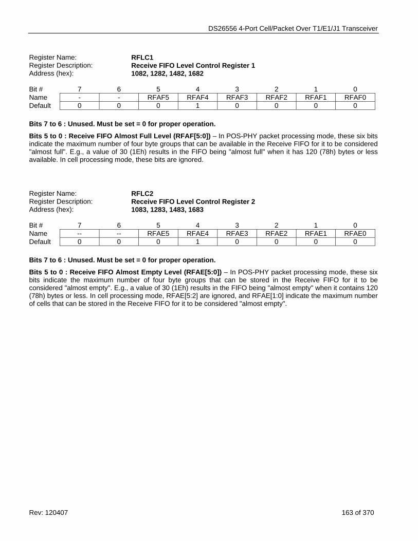
DS26556 4-Port Cell/Packet Over T1/E1/J1 Transceiver
Rev: 120407 163 of 370
Register Name: RFLC1 Register Description: Receive FIFO Level Control Register 1 Address (hex): 1082, 1282, 1482, 1682 Bit # 7 6 5 4 3 2 1 0 Name - - RFAF5 RFAF4 RFAF3 RFAF2 RFAF1 RFAF0 Default 0 0 0 1 0 0 0 0 Bits 7 to 6 : Unused. Must be set = 0 for proper operation.
Bits 5 to 0 : Receive FIFO Almost Full Level (RFAF[5:0]) – In POS-PHY packet processing mode, these six bits indicate the maximum number of four byte groups that can be available in the Receive FIFO for it to be considered "almost full". E.g., a value of 30 (1Eh) results in the FIFO being "almost full" when it has 120 (78h) bytes or less available. In cell processing mode, these bits are ignored.
Register Name: RFLC2 Register Description: Receive FIFO Level Control Register 2 Address (hex): 1083, 1283, 1483, 1683 Bit # 7 6 5 4 3 2 1 0 Name -- -- RFAE5 RFAE4 RFAE3 RFAE2 RFAE1 RFAE0 Default 0 0 0 1 0 0 0 0 Bits 7 to 6 : Unused. Must be set = 0 for proper operation.
Bits 5 to 0 : Receive FIFO Almost Empty Level (RFAE[5:0]) – In POS-PHY packet processing mode, these six bits indicate the maximum number of four byte groups that can be stored in the Receive FIFO for it to be considered "almost empty". E.g., a value of 30 (1Eh) results in the FIFO being "almost empty" when it contains 120 (78h) bytes or less. In cell processing mode, RFAE[5:2] are ignored, and RFAE[1:0] indicate the maximum number of cells that can be stored in the Receive FIFO for it to be considered "almost empty".
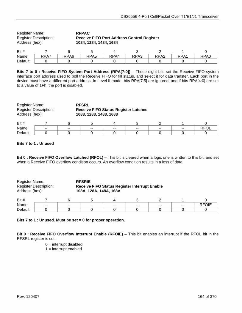
DS26556 4-Port Cell/Packet Over T1/E1/J1 Transceiver
Rev: 120407 164 of 370
Register Name: RFPAC Register Description: Receive FIFO Port Address Control Register Address (hex): 1084, 1284, 1484, 1684 Bit # 7 6 5 4 3 2 1 0 Name RPA7 RPA6 RPA5 RPA4 RPA3 RPA2 RPA1 RPA0 Default 0 0 0 0 0 0 0 0 Bits 7 to 0 : Receive FIFO System Port Address (RPA[7:0]) – These eight bits set the Receive FIFO system interface port address used to poll the Receive FIFO for fill status, and select it for data transfer. Each port in the device must have a different port address. In Level II mode, bits RPA[7:5] are ignored, and if bits RPA[4:0] are set to a value of 1Fh, the port is disabled.
Register Name: RFSRL Register Description: Receive FIFO Status Register Latched Address (hex): 1088, 1288, 1488, 1688 Bit # 7 6 5 4 3 2 1 0 Name -- -- -- -- -- -- -- RFOL Default 0 0 0 0 0 0 0 0 Bits 7 to 1 : Unused
Bit 0 : Receive FIFO Overflow Latched (RFOL) – This bit is cleared when a logic one is written to this bit, and set when a Receive FIFO overflow condition occurs. An overflow condition results in a loss of data.
Register Name: RFSRIE Register Description: Receive FIFO Status Register Interrupt Enable Address (hex): 108A, 128A, 148A, 168A Bit # 7 6 5 4 3 2 1 0 Name -- -- -- -- -- -- -- RFOIE Default 0 0 0 0 0 0 0 0 Bits 7 to 1 : Unused. Must be set = 0 for proper operation.
Bit 0 : Receive FIFO Overflow Interrupt Enable (RFOIE) – This bit enables an interrupt if the RFOL bit in the RFSRL register is set.
0 = interrupt disabled 1 = interrupt enabled
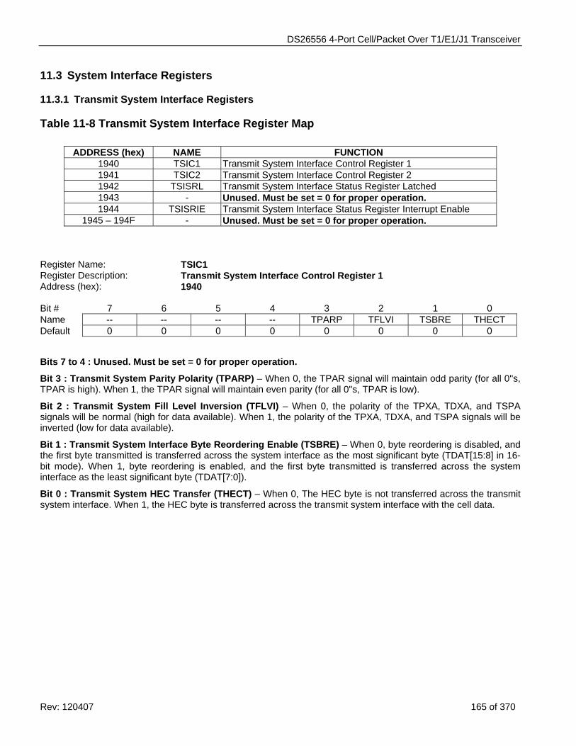
DS26556 4-Port Cell/Packet Over T1/E1/J1 Transceiver
Rev: 120407 165 of 370
11.3 System Interface Registers
11.3.1 Transmit System Interface Registers
Table 11-8 Transmit System Interface Register Map
ADDRESS (hex) NAME FUNCTION 1940 TSIC1 Transmit System Interface Control Register 1 1941 TSIC2 Transmit System Interface Control Register 2 1942 TSISRL Transmit System Interface Status Register Latched 1943 - Unused. Must be set = 0 for proper operation. 1944 TSISRIE Transmit System Interface Status Register Interrupt Enable
1945 – 194F - Unused. Must be set = 0 for proper operation. Register Name: TSIC1 Register Description: Transmit System Interface Control Register 1 Address (hex): 1940 Bit # 7 6 5 4 3 2 1 0 Name -- -- -- -- TPARP TFLVI TSBRE THECT Default 0 0 0 0 0 0 0 0
Bits 7 to 4 : Unused. Must be set = 0 for proper operation.
Bit 3 : Transmit System Parity Polarity (TPARP) – When 0, the TPAR signal will maintain odd parity (for all 0''s, TPAR is high). When 1, the TPAR signal will maintain even parity (for all 0''s, TPAR is low).
Bit 2 : Transmit System Fill Level Inversion (TFLVI) – When 0, the polarity of the TPXA, TDXA, and TSPA signals will be normal (high for data available). When 1, the polarity of the TPXA, TDXA, and TSPA signals will be inverted (low for data available).
Bit 1 : Transmit System Interface Byte Reordering Enable (TSBRE) – When 0, byte reordering is disabled, and the first byte transmitted is transferred across the system interface as the most significant byte (TDAT[15:8] in 16-bit mode). When 1, byte reordering is enabled, and the first byte transmitted is transferred across the system interface as the least significant byte (TDAT[7:0]).
Bit 0 : Transmit System HEC Transfer (THECT) – When 0, The HEC byte is not transferred across the transmit system interface. When 1, the HEC byte is transferred across the transmit system interface with the cell data.
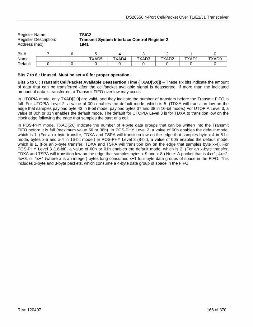
DS26556 4-Port Cell/Packet Over T1/E1/J1 Transceiver
Rev: 120407 166 of 370
Register Name: TSIC2 Register Description: Transmit System Interface Control Register 2 Address (hex): 1941 Bit # 7 6 5 4 3 2 1 0 Name -- -- TXAD5 TXAD4 TXAD3 TXAD2 TXAD1 TXAD0 Default 0 0 0 0 0 0 0 0 Bits 7 to 6 : Unused. Must be set = 0 for proper operation.
Bits 5 to 0 : Transmit Cell/Packet Available Deassertion Time (TXAD[5:0]) – These six bits indicate the amount of data that can be transferred after the cell/packet available signal is deasserted. If more than the indicated amount of data is transferred, a Transmit FIFO overflow may occur.
In UTOPIA mode, only TXAD[2:0] are valid, and they indicate the number of transfers before the Transmit FIFO is full. For UTOPIA Level 2, a value of 00h enables the default mode, which is 5. (TDXA will transition low on the edge that samples payload byte 43 in 8-bit mode, payload bytes 37 and 38 in 16-bit mode.) For UTOPIA Level 3, a value of 00h or 01h enables the default mode. The default for UTOPIA Level 3 is for TDXA to transition low on the clock edge following the edge that samples the start of a cell.
In POS-PHY mode, TXAD[5:0] indicate the number of 4-byte data groups that can be written into the Transmit FIFO before it is full (maximum value 56 or 38h). In POS-PHY Level 2, a value of 00h enables the default mode, which is 1. (For an x-byte transfer, TDXA and TSPA will transition low on the edge that samples byte x-4 in 8-bit mode, bytes x-5 and x-4 in 16-bit mode.) In POS-PHY Level 3 (8-bit), a value of 00h enables the default mode, which is 1. (For an x-byte transfer, TDXA and TSPA will transition low on the edge that samples byte x-4). For POS-PHY Level 3 (16-bit), a value of 00h or 01h enables the default mode, which is 2. (For an x-byte transfer, TDXA and TSPA will transition low on the edge that samples bytes x-9 and x-8.) Note: A packet that is 4x+1, 4x+2, 4x+3, or 4x+4 (where x is an integer) bytes long consumes x+1 four byte data groups of space in the FIFO. This includes 2-byte and 3-byte packets, which consume a 4-byte data group of space in the FIFO.
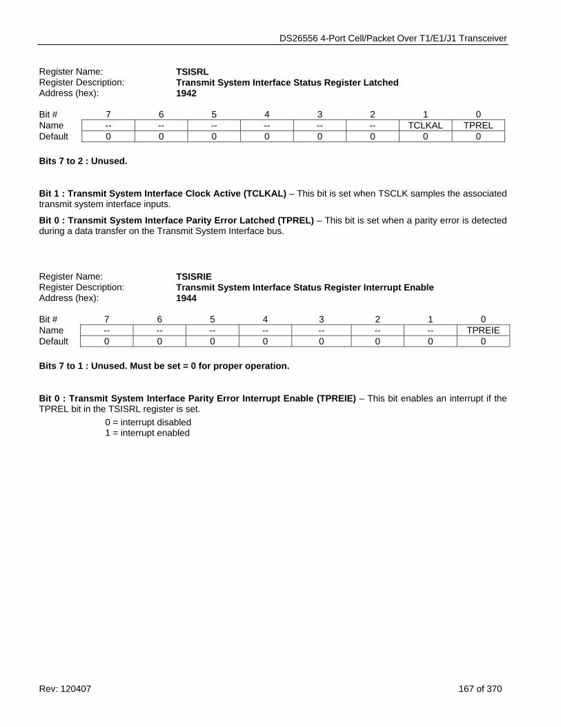
DS26556 4-Port Cell/Packet Over T1/E1/J1 Transceiver
Rev: 120407 167 of 370
Register Name: TSISRL Register Description: Transmit System Interface Status Register Latched Address (hex): 1942 Bit # 7 6 5 4 3 2 1 0 Name -- -- -- -- -- -- TCLKAL TPREL Default 0 0 0 0 0 0 0 0 Bits 7 to 2 : Unused.
Bit 1 : Transmit System Interface Clock Active (TCLKAL) – This bit is set when TSCLK samples the associated transmit system interface inputs.
Bit 0 : Transmit System Interface Parity Error Latched (TPREL) – This bit is set when a parity error is detected during a data transfer on the Transmit System Interface bus.
Register Name: TSISRIE Register Description: Transmit System Interface Status Register Interrupt Enable Address (hex): 1944 Bit # 7 6 5 4 3 2 1 0 Name -- -- -- -- -- -- -- TPREIE Default 0 0 0 0 0 0 0 0 Bits 7 to 1 : Unused. Must be set = 0 for proper operation.
Bit 0 : Transmit System Interface Parity Error Interrupt Enable (TPREIE) – This bit enables an interrupt if the TPREL bit in the TSISRL register is set.
0 = interrupt disabled 1 = interrupt enabled
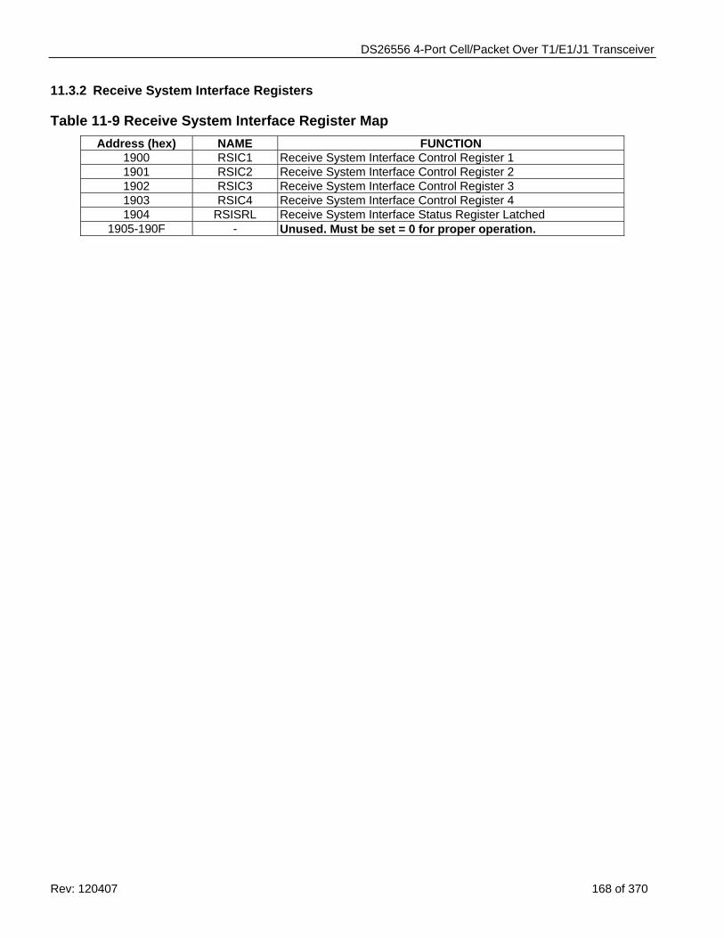
DS26556 4-Port Cell/Packet Over T1/E1/J1 Transceiver
Rev: 120407 168 of 370
11.3.2 Receive System Interface Registers
Table 11-9 Receive System Interface Register Map Address (hex) NAME FUNCTION
1900 RSIC1 Receive System Interface Control Register 1 1901 RSIC2 Receive System Interface Control Register 2 1902 RSIC3 Receive System Interface Control Register 3 1903 RSIC4 Receive System Interface Control Register 4 1904 RSISRL Receive System Interface Status Register Latched
1905-190F - Unused. Must be set = 0 for proper operation.
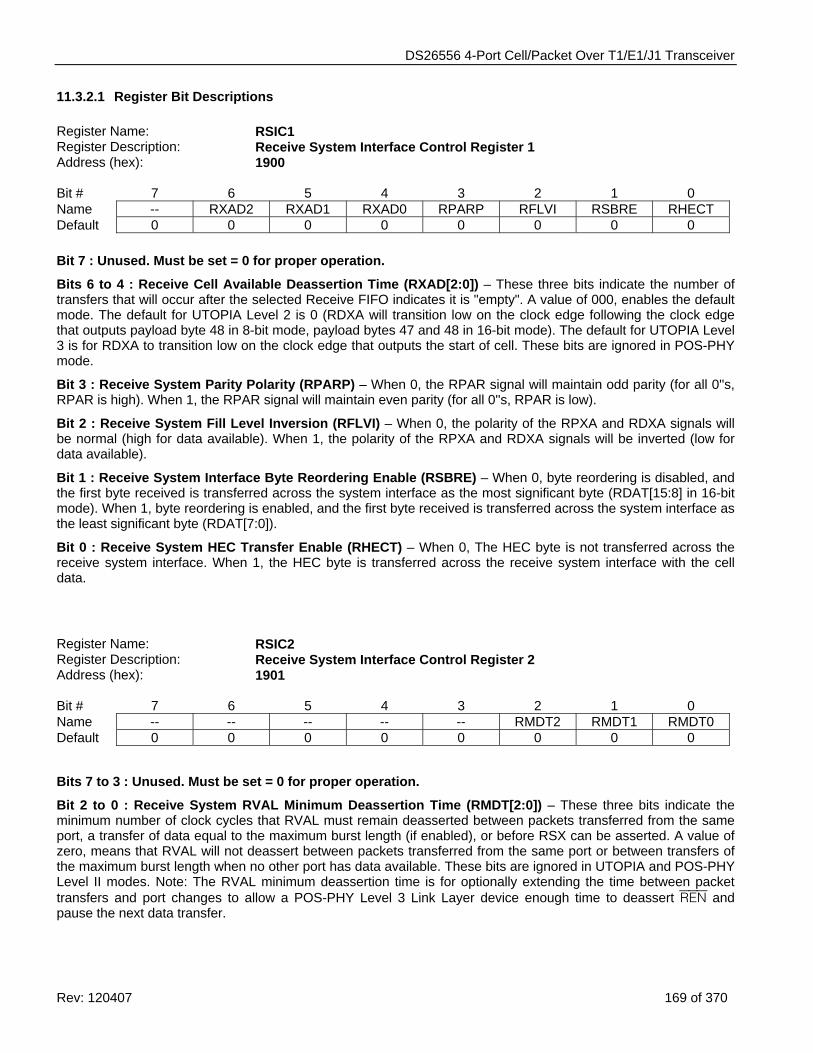
DS26556 4-Port Cell/Packet Over T1/E1/J1 Transceiver
Rev: 120407 169 of 370
11.3.2.1 Register Bit Descriptions Register Name: RSIC1 Register Description: Receive System Interface Control Register 1 Address (hex): 1900 Bit # 7 6 5 4 3 2 1 0 Name -- RXAD2 RXAD1 RXAD0 RPARP RFLVI RSBRE RHECT Default 0 0 0 0 0 0 0 0 Bit 7 : Unused. Must be set = 0 for proper operation.
Bits 6 to 4 : Receive Cell Available Deassertion Time (RXAD[2:0]) – These three bits indicate the number of transfers that will occur after the selected Receive FIFO indicates it is "empty". A value of 000, enables the default mode. The default for UTOPIA Level 2 is 0 (RDXA will transition low on the clock edge following the clock edge that outputs payload byte 48 in 8-bit mode, payload bytes 47 and 48 in 16-bit mode). The default for UTOPIA Level 3 is for RDXA to transition low on the clock edge that outputs the start of cell. These bits are ignored in POS-PHY mode.
Bit 3 : Receive System Parity Polarity (RPARP) – When 0, the RPAR signal will maintain odd parity (for all 0''s, RPAR is high). When 1, the RPAR signal will maintain even parity (for all 0''s, RPAR is low).
Bit 2 : Receive System Fill Level Inversion (RFLVI) – When 0, the polarity of the RPXA and RDXA signals will be normal (high for data available). When 1, the polarity of the RPXA and RDXA signals will be inverted (low for data available).
Bit 1 : Receive System Interface Byte Reordering Enable (RSBRE) – When 0, byte reordering is disabled, and the first byte received is transferred across the system interface as the most significant byte (RDAT[15:8] in 16-bit mode). When 1, byte reordering is enabled, and the first byte received is transferred across the system interface as the least significant byte (RDAT[7:0]).
Bit 0 : Receive System HEC Transfer Enable (RHECT) – When 0, The HEC byte is not transferred across the receive system interface. When 1, the HEC byte is transferred across the receive system interface with the cell data.
Register Name: RSIC2 Register Description: Receive System Interface Control Register 2 Address (hex): 1901 Bit # 7 6 5 4 3 2 1 0 Name -- -- -- -- -- RMDT2 RMDT1 RMDT0 Default 0 0 0 0 0 0 0 0
Bits 7 to 3 : Unused. Must be set = 0 for proper operation.
Bit 2 to 0 : Receive System RVAL Minimum Deassertion Time (RMDT[2:0]) – These three bits indicate the minimum number of clock cycles that RVAL must remain deasserted between packets transferred from the same port, a transfer of data equal to the maximum burst length (if enabled), or before RSX can be asserted. A value of zero, means that RVAL will not deassert between packets transferred from the same port or between transfers of the maximum burst length when no other port has data available. These bits are ignored in UTOPIA and POS-PHY Level II modes. Note: The RVAL minimum deassertion time is for optionally extending the time between packet transfers and port changes to allow a POS-PHY Level 3 Link Layer device enough time to deassert REN and pause the next data transfer.
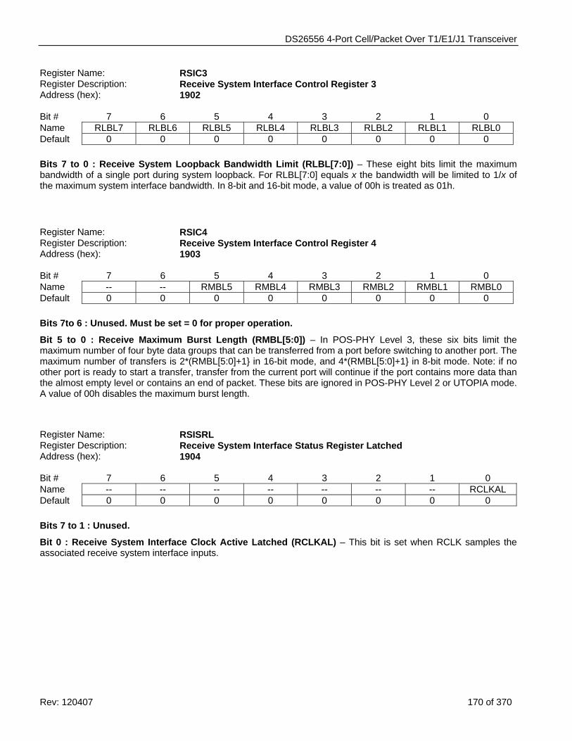
DS26556 4-Port Cell/Packet Over T1/E1/J1 Transceiver
Rev: 120407 170 of 370
Register Name: RSIC3 Register Description: Receive System Interface Control Register 3 Address (hex): 1902 Bit # 7 6 5 4 3 2 1 0 Name RLBL7 RLBL6 RLBL5 RLBL4 RLBL3 RLBL2 RLBL1 RLBL0 Default 0 0 0 0 0 0 0 0 Bits 7 to 0 : Receive System Loopback Bandwidth Limit (RLBL[7:0]) – These eight bits limit the maximum bandwidth of a single port during system loopback. For RLBL[7:0] equals x the bandwidth will be limited to 1/x of the maximum system interface bandwidth. In 8-bit and 16-bit mode, a value of 00h is treated as 01h.
Register Name: RSIC4 Register Description: Receive System Interface Control Register 4 Address (hex): 1903 Bit # 7 6 5 4 3 2 1 0 Name -- -- RMBL5 RMBL4 RMBL3 RMBL2 RMBL1 RMBL0 Default 0 0 0 0 0 0 0 0 Bits 7to 6 : Unused. Must be set = 0 for proper operation.
Bit 5 to 0 : Receive Maximum Burst Length (RMBL[5:0]) – In POS-PHY Level 3, these six bits limit the maximum number of four byte data groups that can be transferred from a port before switching to another port. The maximum number of transfers is 2*(RMBL[5:0]+1} in 16-bit mode, and 4*(RMBL[5:0]+1} in 8-bit mode. Note: if no other port is ready to start a transfer, transfer from the current port will continue if the port contains more data than the almost empty level or contains an end of packet. These bits are ignored in POS-PHY Level 2 or UTOPIA mode. A value of 00h disables the maximum burst length. Register Name: RSISRL Register Description: Receive System Interface Status Register Latched Address (hex): 1904 Bit # 7 6 5 4 3 2 1 0 Name -- -- -- -- -- -- -- RCLKAL Default 0 0 0 0 0 0 0 0 Bits 7 to 1 : Unused.
Bit 0 : Receive System Interface Clock Active Latched (RCLKAL) – This bit is set when RCLK samples the associated receive system interface inputs.
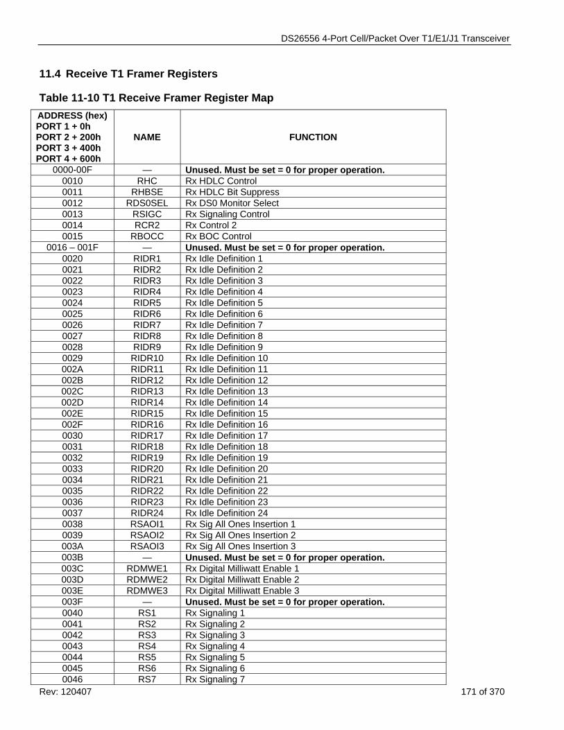
DS26556 4-Port Cell/Packet Over T1/E1/J1 Transceiver
Rev: 120407 171 of 370
11.4 Receive T1 Framer Registers
Table 11-10 T1 Receive Framer Register Map ADDRESS (hex) PORT 1 + 0h PORT 2 + 200h PORT 3 + 400h PORT 4 + 600h
NAME FUNCTION
0000-00F — Unused. Must be set = 0 for proper operation. 0010 RHC Rx HDLC Control 0011 RHBSE Rx HDLC Bit Suppress 0012 RDS0SEL Rx DS0 Monitor Select 0013 RSIGC Rx Signaling Control 0014 RCR2 Rx Control 2 0015 RBOCC Rx BOC Control
0016 – 001F — Unused. Must be set = 0 for proper operation. 0020 RIDR1 Rx Idle Definition 1 0021 RIDR2 Rx Idle Definition 2 0022 RIDR3 Rx Idle Definition 3 0023 RIDR4 Rx Idle Definition 4 0024 RIDR5 Rx Idle Definition 5 0025 RIDR6 Rx Idle Definition 6 0026 RIDR7 Rx Idle Definition 7 0027 RIDR8 Rx Idle Definition 8 0028 RIDR9 Rx Idle Definition 9 0029 RIDR10 Rx Idle Definition 10 002A RIDR11 Rx Idle Definition 11 002B RIDR12 Rx Idle Definition 12 002C RIDR13 Rx Idle Definition 13 002D RIDR14 Rx Idle Definition 14 002E RIDR15 Rx Idle Definition 15 002F RIDR16 Rx Idle Definition 16 0030 RIDR17 Rx Idle Definition 17 0031 RIDR18 Rx Idle Definition 18 0032 RIDR19 Rx Idle Definition 19 0033 RIDR20 Rx Idle Definition 20 0034 RIDR21 Rx Idle Definition 21 0035 RIDR22 Rx Idle Definition 22 0036 RIDR23 Rx Idle Definition 23 0037 RIDR24 Rx Idle Definition 24 0038 RSAOI1 Rx Sig All Ones Insertion 1 0039 RSAOI2 Rx Sig All Ones Insertion 2 003A RSAOI3 Rx Sig All Ones Insertion 3 003B — Unused. Must be set = 0 for proper operation. 003C RDMWE1 Rx Digital Milliwatt Enable 1 003D RDMWE2 Rx Digital Milliwatt Enable 2 003E RDMWE3 Rx Digital Milliwatt Enable 3 003F — Unused. Must be set = 0 for proper operation. 0040 RS1 Rx Signaling 1 0041 RS2 Rx Signaling 2 0042 RS3 Rx Signaling 3 0043 RS4 Rx Signaling 4 0044 RS5 Rx Signaling 5 0045 RS6 Rx Signaling 6 0046 RS7 Rx Signaling 7
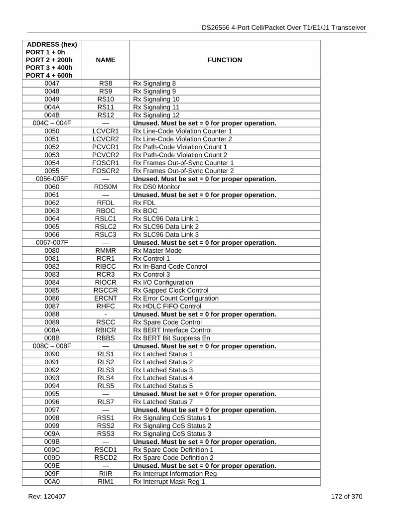
DS26556 4-Port Cell/Packet Over T1/E1/J1 Transceiver
Rev: 120407 172 of 370
ADDRESS (hex) PORT 1 + 0h PORT 2 + 200h PORT 3 + 400h PORT 4 + 600h
NAME FUNCTION
0047 RS8 Rx Signaling 8 0048 RS9 Rx Signaling 9 0049 RS10 Rx Signaling 10 004A RS11 Rx Signaling 11 004B RS12 Rx Signaling 12
004C – 004F — Unused. Must be set = 0 for proper operation. 0050 LCVCR1 Rx Line-Code Violation Counter 1 0051 LCVCR2 Rx Line-Code Violation Counter 2 0052 PCVCR1 Rx Path-Code Violation Count 1 0053 PCVCR2 Rx Path-Code Violation Count 2 0054 FOSCR1 Rx Frames Out-of-Sync Counter 1 0055 FOSCR2 Rx Frames Out-of-Sync Counter 2
0056-005F — Unused. Must be set = 0 for proper operation. 0060 RDS0M Rx DS0 Monitor 0061 — Unused. Must be set = 0 for proper operation. 0062 RFDL Rx FDL 0063 RBOC Rx BOC 0064 RSLC1 Rx SLC96 Data Link 1 0065 RSLC2 Rx SLC96 Data Link 2 0066 RSLC3 Rx SLC96 Data Link 3
0067-007F — Unused. Must be set = 0 for proper operation. 0080 RMMR Rx Master Mode 0081 RCR1 Rx Control 1 0082 RIBCC Rx In-Band Code Control 0083 RCR3 Rx Control 3 0084 RIOCR Rx I/O Configuration 0085 RGCCR Rx Gapped Clock Control 0086 ERCNT Rx Error Count Configuration 0087 RHFC Rx HDLC FIFO Control 0088 - Unused. Must be set = 0 for proper operation. 0089 RSCC Rx Spare Code Control 008A RBICR Rx BERT Interface Control 008B RBBS Rx BERT Bit Suppress En
008C – 008F — Unused. Must be set = 0 for proper operation. 0090 RLS1 Rx Latched Status 1 0091 RLS2 Rx Latched Status 2 0092 RLS3 Rx Latched Status 3 0093 RLS4 Rx Latched Status 4 0094 RLS5 Rx Latched Status 5 0095 — Unused. Must be set = 0 for proper operation. 0096 RLS7 Rx Latched Status 7 0097 — Unused. Must be set = 0 for proper operation. 0098 RSS1 Rx Signaling CoS Status 1 0099 RSS2 Rx Signaling CoS Status 2 009A RSS3 Rx Signaling CoS Status 3 009B — Unused. Must be set = 0 for proper operation. 009C RSCD1 Rx Spare Code Definition 1 009D RSCD2 Rx Spare Code Definition 2 009E — Unused. Must be set = 0 for proper operation. 009F RIIR Rx Interrupt Information Reg 00A0 RIM1 Rx Interrupt Mask Reg 1
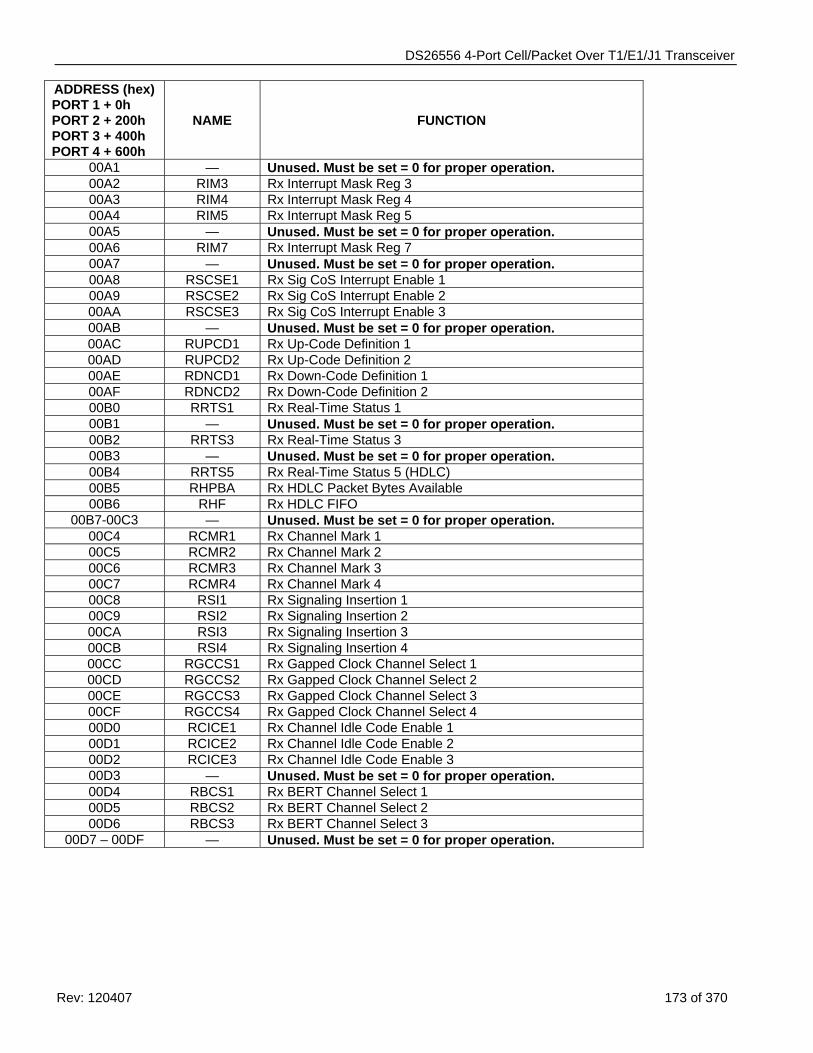
DS26556 4-Port Cell/Packet Over T1/E1/J1 Transceiver
Rev: 120407 173 of 370
ADDRESS (hex) PORT 1 + 0h PORT 2 + 200h PORT 3 + 400h PORT 4 + 600h
NAME FUNCTION
00A1 — Unused. Must be set = 0 for proper operation. 00A2 RIM3 Rx Interrupt Mask Reg 3 00A3 RIM4 Rx Interrupt Mask Reg 4 00A4 RIM5 Rx Interrupt Mask Reg 5 00A5 — Unused. Must be set = 0 for proper operation. 00A6 RIM7 Rx Interrupt Mask Reg 7 00A7 — Unused. Must be set = 0 for proper operation. 00A8 RSCSE1 Rx Sig CoS Interrupt Enable 1 00A9 RSCSE2 Rx Sig CoS Interrupt Enable 2 00AA RSCSE3 Rx Sig CoS Interrupt Enable 3 00AB — Unused. Must be set = 0 for proper operation. 00AC RUPCD1 Rx Up-Code Definition 1 00AD RUPCD2 Rx Up-Code Definition 2 00AE RDNCD1 Rx Down-Code Definition 1 00AF RDNCD2 Rx Down-Code Definition 2 00B0 RRTS1 Rx Real-Time Status 1 00B1 — Unused. Must be set = 0 for proper operation. 00B2 RRTS3 Rx Real-Time Status 3 00B3 — Unused. Must be set = 0 for proper operation. 00B4 RRTS5 Rx Real-Time Status 5 (HDLC) 00B5 RHPBA Rx HDLC Packet Bytes Available 00B6 RHF Rx HDLC FIFO
00B7-00C3 — Unused. Must be set = 0 for proper operation. 00C4 RCMR1 Rx Channel Mark 1 00C5 RCMR2 Rx Channel Mark 2 00C6 RCMR3 Rx Channel Mark 3 00C7 RCMR4 Rx Channel Mark 4 00C8 RSI1 Rx Signaling Insertion 1 00C9 RSI2 Rx Signaling Insertion 2 00CA RSI3 Rx Signaling Insertion 3 00CB RSI4 Rx Signaling Insertion 4 00CC RGCCS1 Rx Gapped Clock Channel Select 1 00CD RGCCS2 Rx Gapped Clock Channel Select 2 00CE RGCCS3 Rx Gapped Clock Channel Select 3 00CF RGCCS4 Rx Gapped Clock Channel Select 4 00D0 RCICE1 Rx Channel Idle Code Enable 1 00D1 RCICE2 Rx Channel Idle Code Enable 2 00D2 RCICE3 Rx Channel Idle Code Enable 3 00D3 — Unused. Must be set = 0 for proper operation. 00D4 RBCS1 Rx BERT Channel Select 1 00D5 RBCS2 Rx BERT Channel Select 2 00D6 RBCS3 Rx BERT Channel Select 3
00D7 – 00DF — Unused. Must be set = 0 for proper operation.
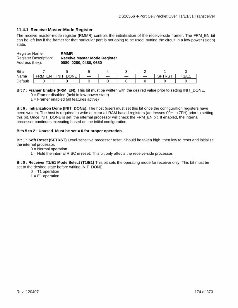
DS26556 4-Port Cell/Packet Over T1/E1/J1 Transceiver
Rev: 120407 174 of 370
11.4.1 Receive Master-Mode Register The receive master-mode register (RMMR) controls the initialization of the receive-side framer. The FRM_EN bit can be left low if the framer for that particular port is not going to be used, putting the circuit in a low-power (sleep) state. Register Name: RMMR Register Description: Receive Master Mode Register Address (hex): 0080, 0280, 0480, 0680 Bit # 7 6 5 4 3 2 1 0 Name FRM_EN INIT_DONE — — — — SFTRST T1/E1 Default 0 0 0 0 0 0 0 0 Bit 7 : Framer Enable (FRM_EN). This bit must be written with the desired value prior to setting INIT_DONE. 0 = Framer disabled (held in low-power state) 1 = Framer enabled (all features active) Bit 6 : Initialization Done (INIT_DONE). The host (user) must set this bit once the configuration registers have been written. The host is required to write or clear all RAM based registers (addresses 00H to 7FH) prior to setting this bit. Once INIT_DONE is set, the internal processor will check the FRM_EN bit. If enabled, the internal processor continues executing based on the initial configuration. Bits 5 to 2 : Unused. Must be set = 0 for proper operation. Bit 1 : Soft Reset (SFTRST) Level-sensitive processor reset. Should be taken high, then low to reset and initialize the internal processor.
0 = Normal operation 1 = Hold the internal RISC in reset. This bit only affects the receive-side processor.
Bit 0 : Receiver T1/E1 Mode Select (T1/E1) This bit sets the operating mode for receiver only! This bit must be set to the desired state before writing INIT_DONE.
0 = T1 operation 1 = E1 operation
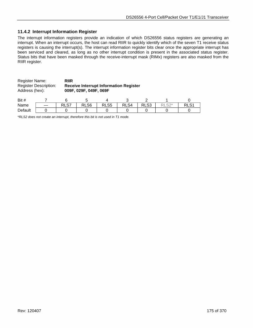
DS26556 4-Port Cell/Packet Over T1/E1/J1 Transceiver
Rev: 120407 175 of 370
11.4.2 Interrupt Information Register The interrupt information registers provide an indication of which DS26556 status registers are generating an interrupt. When an interrupt occurs, the host can read RIIR to quickly identify which of the seven T1 receive status registers is causing the interrupt(s). The interrupt information register bits clear once the appropriate interrupt has been serviced and cleared, as long as no other interrupt condition is present in the associated status register. Status bits that have been masked through the receive-interrupt mask (RIMx) registers are also masked from the RIIR register. Register Name: RIIR Register Description: Receive Interrupt Information Register Address (hex): 009F, 029F, 049F, 069F Bit # 7 6 5 4 3 2 1 0 Name — RLS7 RLS6 RLS5 RLS4 RLS3 RLS2* RLS1 Default 0 0 0 0 0 0 0 0 *RLS2 does not create an interrupt, therefore this bit is not used in T1 mode.
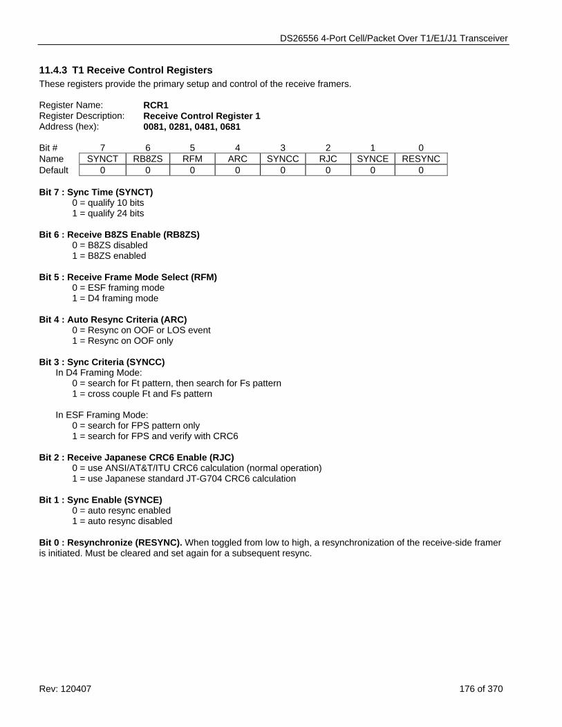
DS26556 4-Port Cell/Packet Over T1/E1/J1 Transceiver
Rev: 120407 176 of 370
11.4.3 T1 Receive Control Registers These registers provide the primary setup and control of the receive framers.
Register Name: RCR1 Register Description: Receive Control Register 1 Address (hex): 0081, 0281, 0481, 0681 Bit # 7 6 5 4 3 2 1 0 Name SYNCT RB8ZS RFM ARC SYNCC RJC SYNCE RESYNC Default 0 0 0 0 0 0 0 0 Bit 7 : Sync Time (SYNCT)
0 = qualify 10 bits 1 = qualify 24 bits
Bit 6 : Receive B8ZS Enable (RB8ZS)
0 = B8ZS disabled 1 = B8ZS enabled
Bit 5 : Receive Frame Mode Select (RFM)
0 = ESF framing mode 1 = D4 framing mode
Bit 4 : Auto Resync Criteria (ARC) 0 = Resync on OOF or LOS event 1 = Resync on OOF only
Bit 3 : Sync Criteria (SYNCC) In D4 Framing Mode:
0 = search for Ft pattern, then search for Fs pattern 1 = cross couple Ft and Fs pattern
In ESF Framing Mode: 0 = search for FPS pattern only 1 = search for FPS and verify with CRC6
Bit 2 : Receive Japanese CRC6 Enable (RJC) 0 = use ANSI/AT&T/ITU CRC6 calculation (normal operation) 1 = use Japanese standard JT-G704 CRC6 calculation
Bit 1 : Sync Enable (SYNCE)
0 = auto resync enabled 1 = auto resync disabled
Bit 0 : Resynchronize (RESYNC). When toggled from low to high, a resynchronization of the receive-side framer is initiated. Must be cleared and set again for a subsequent resync.
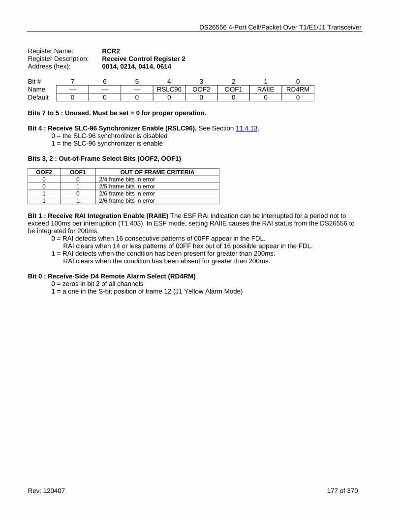
DS26556 4-Port Cell/Packet Over T1/E1/J1 Transceiver
Rev: 120407 177 of 370
Register Name: RCR2 Register Description: Receive Control Register 2 Address (hex): 0014, 0214, 0414, 0614 Bit # 7 6 5 4 3 2 1 0 Name — — — RSLC96 OOF2 OOF1 RAIIE RD4RM Default 0 0 0 0 0 0 0 0 Bits 7 to 5 : Unused. Must be set = 0 for proper operation. Bit 4 : Receive SLC-96 Synchronizer Enable (RSLC96). See Section 11.4.13.
0 = the SLC-96 synchronizer is disabled 1 = the SLC-96 synchronizer is enable
Bits 3, 2 : Out-of-Frame Select Bits (OOF2, OOF1)
OOF2 OOF1 OUT OF FRAME CRITERIA 0 0 2/4 frame bits in error 0 1 2/5 frame bits in error 1 0 2/6 frame bits in error 1 1 2/6 frame bits in error
Bit 1 : Receive RAI Integration Enable (RAIIE) The ESF RAI indication can be interrupted for a period not to exceed 100ms per interruption (T1.403). In ESF mode, setting RAIIE causes the RAI status from the DS26556 to be integrated for 200ms. 0 = RAI detects when 16 consecutive patterns of 00FF appear in the FDL.
RAI clears when 14 or less patterns of 00FF hex out of 16 possible appear in the FDL. 1 = RAI detects when the condition has been present for greater than 200ms.
RAI clears when the condition has been absent for greater than 200ms. Bit 0 : Receive-Side D4 Remote Alarm Select (RD4RM)
0 = zeros in bit 2 of all channels 1 = a one in the S-bit position of frame 12 (J1 Yellow Alarm Mode)
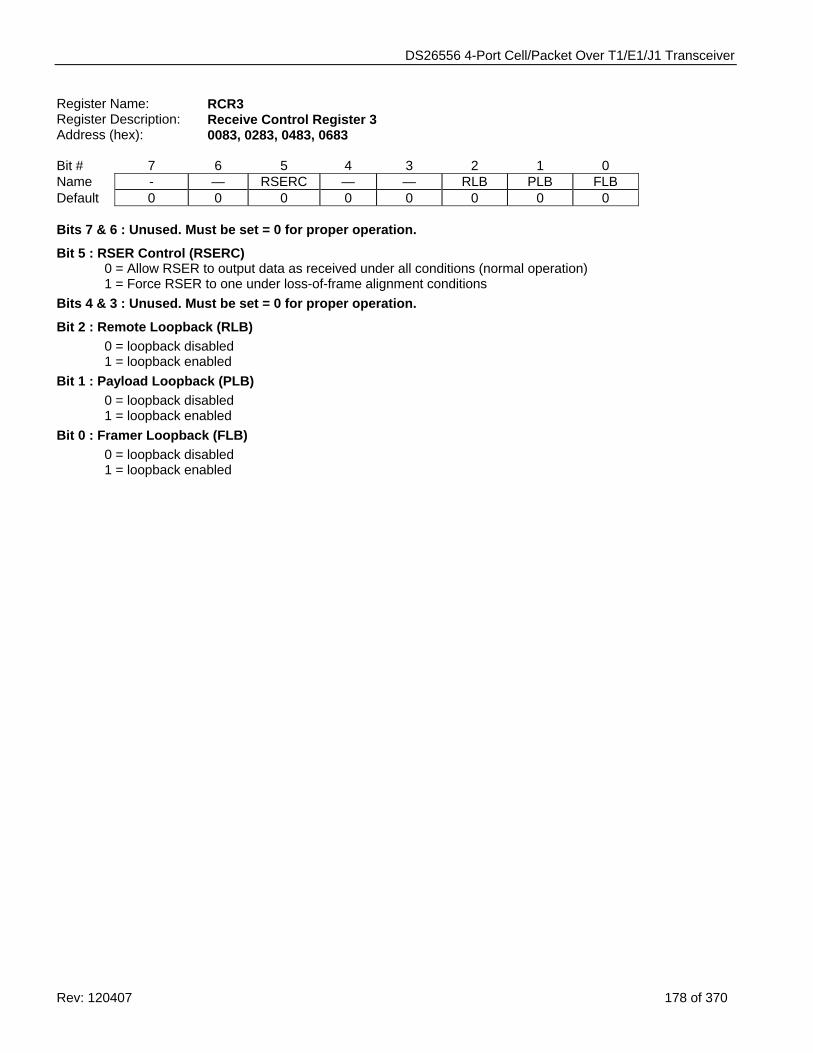
DS26556 4-Port Cell/Packet Over T1/E1/J1 Transceiver
Rev: 120407 178 of 370
Register Name: RCR3 Register Description: Receive Control Register 3 Address (hex): 0083, 0283, 0483, 0683 Bit # 7 6 5 4 3 2 1 0 Name - — RSERC — — RLB PLB FLB Default 0 0 0 0 0 0 0 0 Bits 7 & 6 : Unused. Must be set = 0 for proper operation.
Bit 5 : RSER Control (RSERC) 0 = Allow RSER to output data as received under all conditions (normal operation) 1 = Force RSER to one under loss-of-frame alignment conditions
Bits 4 & 3 : Unused. Must be set = 0 for proper operation.
Bit 2 : Remote Loopback (RLB) 0 = loopback disabled 1 = loopback enabled
Bit 1 : Payload Loopback (PLB) 0 = loopback disabled 1 = loopback enabled
Bit 0 : Framer Loopback (FLB) 0 = loopback disabled 1 = loopback enabled
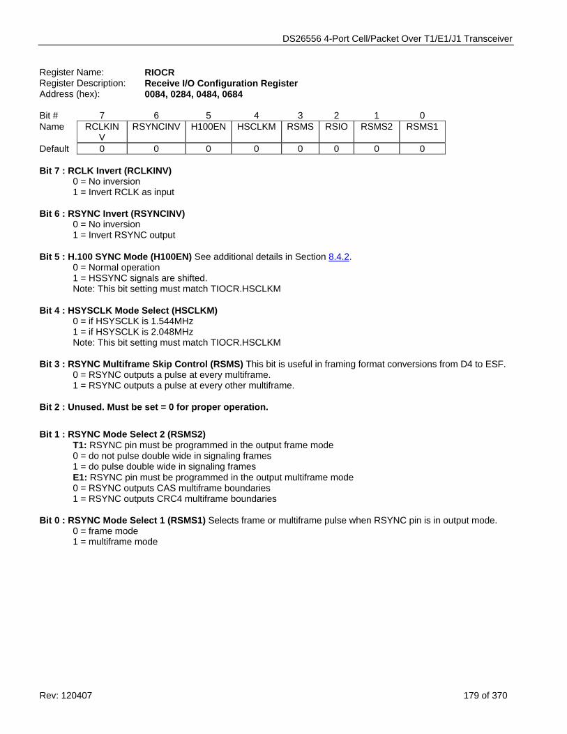
DS26556 4-Port Cell/Packet Over T1/E1/J1 Transceiver
Rev: 120407 179 of 370
Register Name: RIOCR Register Description: Receive I/O Configuration Register Address (hex): 0084, 0284, 0484, 0684 Bit # 7 6 5 4 3 2 1 0 Name RCLKIN
V RSYNCINV H100EN HSCLKM RSMS RSIO RSMS2 RSMS1
Default 0 0 0 0 0 0 0 0 Bit 7 : RCLK Invert (RCLKINV)
0 = No inversion 1 = Invert RCLK as input
Bit 6 : RSYNC Invert (RSYNCINV) 0 = No inversion 1 = Invert RSYNC output
Bit 5 : H.100 SYNC Mode (H100EN) See additional details in Section 8.4.2.
0 = Normal operation 1 = HSSYNC signals are shifted. Note: This bit setting must match TIOCR.HSCLKM
Bit 4 : HSYSCLK Mode Select (HSCLKM) 0 = if HSYSCLK is 1.544MHz 1 = if HSYSCLK is 2.048MHz Note: This bit setting must match TIOCR.HSCLKM
Bit 3 : RSYNC Multiframe Skip Control (RSMS) This bit is useful in framing format conversions from D4 to ESF.
0 = RSYNC outputs a pulse at every multiframe. 1 = RSYNC outputs a pulse at every other multiframe.
Bit 2 : Unused. Must be set = 0 for proper operation.
Bit 1 : RSYNC Mode Select 2 (RSMS2)
T1: RSYNC pin must be programmed in the output frame mode 0 = do not pulse double wide in signaling frames 1 = do pulse double wide in signaling frames E1: RSYNC pin must be programmed in the output multiframe mode 0 = RSYNC outputs CAS multiframe boundaries 1 = RSYNC outputs CRC4 multiframe boundaries
Bit 0 : RSYNC Mode Select 1 (RSMS1) Selects frame or multiframe pulse when RSYNC pin is in output mode.
0 = frame mode 1 = multiframe mode
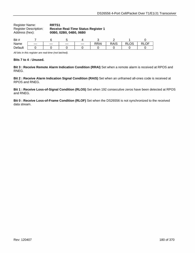
DS26556 4-Port Cell/Packet Over T1/E1/J1 Transceiver
Rev: 120407 180 of 370
Register Name: RRTS1 Register Description: Receive Real-Time Status Register 1 Address (hex): 00B0, 02B0, 04B0, 06B0 Bit # 7 6 5 4 3 2 1 0 Name — — — — RRAI RAIS RLOS RLOF Default 0 0 0 0 0 0 0 0 All bits in this register are real-time (not latched). Bits 7 to 4 : Unused. Bit 3 : Receive Remote Alarm Indication Condition (RRAI) Set when a remote alarm is received at RPOS and RNEG. Bit 2 : Receive Alarm Indication Signal Condition (RAIS) Set when an unframed all-ones code is received at RPOS and RNEG. Bit 1 : Receive Loss-of-Signal Condition (RLOS) Set when 192 consecutive zeros have been detected at RPOS and RNEG. Bit 0 : Receive Loss-of-Frame Condition (RLOF) Set when the DS26556 is not synchronized to the received data stream.
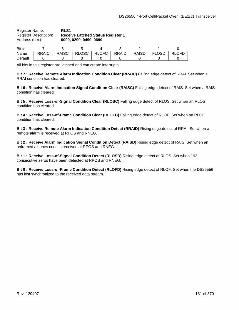
DS26556 4-Port Cell/Packet Over T1/E1/J1 Transceiver
Rev: 120407 181 of 370
Register Name: RLS1 Register Description: Receive Latched Status Register 1 Address (hex): 0090, 0290, 0490, 0690 Bit # 7 6 5 4 3 2 1 0 Name RRAIC RAISC RLOSC RLOFC RRAID RAISD FLOSD RLOFD Default 0 0 0 0 0 0 0 0
All bits in this register are latched and can create interrupts. Bit 7 : Receive Remote Alarm Indication Condition Clear (RRAIC) Falling edge detect of RRAI. Set when a RRAI condition has cleared. Bit 6 : Receive Alarm Indication Signal Condition Clear (RAISC) Falling edge detect of RAIS. Set when a RAIS condition has cleared. Bit 5 : Receive Loss-of-Signal Condition Clear (RLOSC) Falling edge detect of RLOS. Set when an RLOS condition has cleared. Bit 4 : Receive Loss-of-Frame Condition Clear (RLOFC) Falling edge detect of RLOF. Set when an RLOF condition has cleared. Bit 3 : Receive Remote Alarm Indication Condition Detect (RRAID) Rising edge detect of RRAI. Set when a remote alarm is received at RPOS and RNEG. Bit 2 : Receive Alarm Indication Signal Condition Detect (RAISD) Rising edge detect of RAIS. Set when an unframed all-ones code is received at RPOS and RNEG. Bit 1 : Receive Loss-of-Signal Condition Detect (RLOSD) Rising edge detect of RLOS. Set when 192 consecutive zeros have been detected at RPOS and RNEG. Bit 0 : Receive Loss-of-Frame Condition Detect (RLOFD) Rising edge detect of RLOF. Set when the DS26556 has lost synchronized to the received data stream.
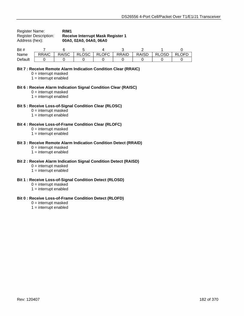
DS26556 4-Port Cell/Packet Over T1/E1/J1 Transceiver
Rev: 120407 182 of 370
Register Name: RIM1 Register Description: Receive Interrupt Mask Register 1 Address (hex): 00A0, 02A0, 04A0, 06A0 Bit # 7 6 5 4 3 2 1 0 Name RRAIC RAISC RLOSC RLOFC RRAID RAISD RLOSD RLOFD Default 0 0 0 0 0 0 0 0 Bit 7 : Receive Remote Alarm Indication Condition Clear (RRAIC)
0 = interrupt masked 1 = interrupt enabled
Bit 6 : Receive Alarm Indication Signal Condition Clear (RAISC) 0 = interrupt masked 1 = interrupt enabled
Bit 5 : Receive Loss-of-Signal Condition Clear (RLOSC)
0 = interrupt masked 1 = interrupt enabled
Bit 4 : Receive Loss-of-Frame Condition Clear (RLOFC)
0 = interrupt masked 1 = interrupt enabled
Bit 3 : Receive Remote Alarm Indication Condition Detect (RRAID)
0 = interrupt masked 1 = interrupt enabled
Bit 2 : Receive Alarm Indication Signal Condition Detect (RAISD)
0 = interrupt masked 1 = interrupt enabled
Bit 1 : Receive Loss-of-Signal Condition Detect (RLOSD)
0 = interrupt masked 1 = interrupt enabled
Bit 0 : Receive Loss-of-Frame Condition Detect (RLOFD)
0 = interrupt masked 1 = interrupt enabled
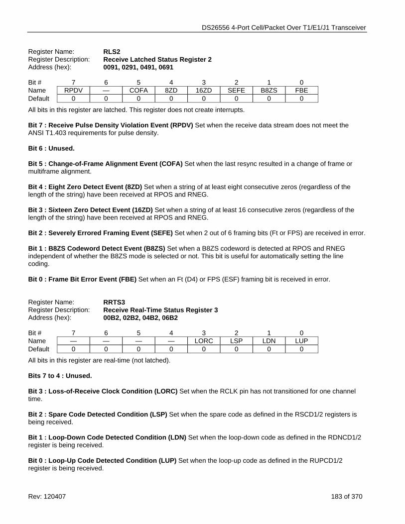
DS26556 4-Port Cell/Packet Over T1/E1/J1 Transceiver
Rev: 120407 183 of 370
Register Name: RLS2 Register Description: Receive Latched Status Register 2 Address (hex): 0091, 0291, 0491, 0691 Bit # 7 6 5 4 3 2 1 0 Name RPDV — COFA 8ZD 16ZD SEFE B8ZS FBE Default 0 0 0 0 0 0 0 0
All bits in this register are latched. This register does not create interrupts. Bit 7 : Receive Pulse Density Violation Event (RPDV) Set when the receive data stream does not meet the ANSI T1.403 requirements for pulse density. Bit 6 : Unused. Bit 5 : Change-of-Frame Alignment Event (COFA) Set when the last resync resulted in a change of frame or multiframe alignment. Bit 4 : Eight Zero Detect Event (8ZD) Set when a string of at least eight consecutive zeros (regardless of the length of the string) have been received at RPOS and RNEG. Bit 3 : Sixteen Zero Detect Event (16ZD) Set when a string of at least 16 consecutive zeros (regardless of the length of the string) have been received at RPOS and RNEG. Bit 2 : Severely Errored Framing Event (SEFE) Set when 2 out of 6 framing bits (Ft or FPS) are received in error. Bit 1 : B8ZS Codeword Detect Event (B8ZS) Set when a B8ZS codeword is detected at RPOS and RNEG independent of whether the B8ZS mode is selected or not. This bit is useful for automatically setting the line coding. Bit 0 : Frame Bit Error Event (FBE) Set when an Ft (D4) or FPS (ESF) framing bit is received in error. Register Name: RRTS3 Register Description: Receive Real-Time Status Register 3 Address (hex): 00B2, 02B2, 04B2, 06B2 Bit # 7 6 5 4 3 2 1 0 Name — — — — LORC LSP LDN LUP Default 0 0 0 0 0 0 0 0
All bits in this register are real-time (not latched). Bits 7 to 4 : Unused. Bit 3 : Loss-of-Receive Clock Condition (LORC) Set when the RCLK pin has not transitioned for one channel time. Bit 2 : Spare Code Detected Condition (LSP) Set when the spare code as defined in the RSCD1/2 registers is being received. Bit 1 : Loop-Down Code Detected Condition (LDN) Set when the loop-down code as defined in the RDNCD1/2 register is being received. Bit 0 : Loop-Up Code Detected Condition (LUP) Set when the loop-up code as defined in the RUPCD1/2 register is being received.
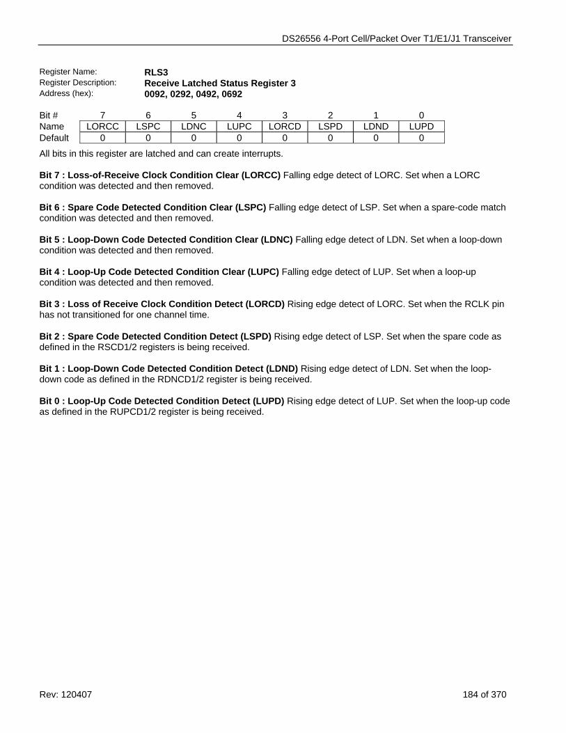
DS26556 4-Port Cell/Packet Over T1/E1/J1 Transceiver
Rev: 120407 184 of 370
Register Name: RLS3 Register Description: Receive Latched Status Register 3 Address (hex): 0092, 0292, 0492, 0692 Bit # 7 6 5 4 3 2 1 0 Name LORCC LSPC LDNC LUPC LORCD LSPD LDND LUPD Default 0 0 0 0 0 0 0 0
All bits in this register are latched and can create interrupts. Bit 7 : Loss-of-Receive Clock Condition Clear (LORCC) Falling edge detect of LORC. Set when a LORC condition was detected and then removed. Bit 6 : Spare Code Detected Condition Clear (LSPC) Falling edge detect of LSP. Set when a spare-code match condition was detected and then removed. Bit 5 : Loop-Down Code Detected Condition Clear (LDNC) Falling edge detect of LDN. Set when a loop-down condition was detected and then removed. Bit 4 : Loop-Up Code Detected Condition Clear (LUPC) Falling edge detect of LUP. Set when a loop-up condition was detected and then removed. Bit 3 : Loss of Receive Clock Condition Detect (LORCD) Rising edge detect of LORC. Set when the RCLK pin has not transitioned for one channel time. Bit 2 : Spare Code Detected Condition Detect (LSPD) Rising edge detect of LSP. Set when the spare code as defined in the RSCD1/2 registers is being received. Bit 1 : Loop-Down Code Detected Condition Detect (LDND) Rising edge detect of LDN. Set when the loop-down code as defined in the RDNCD1/2 register is being received. Bit 0 : Loop-Up Code Detected Condition Detect (LUPD) Rising edge detect of LUP. Set when the loop-up code as defined in the RUPCD1/2 register is being received.
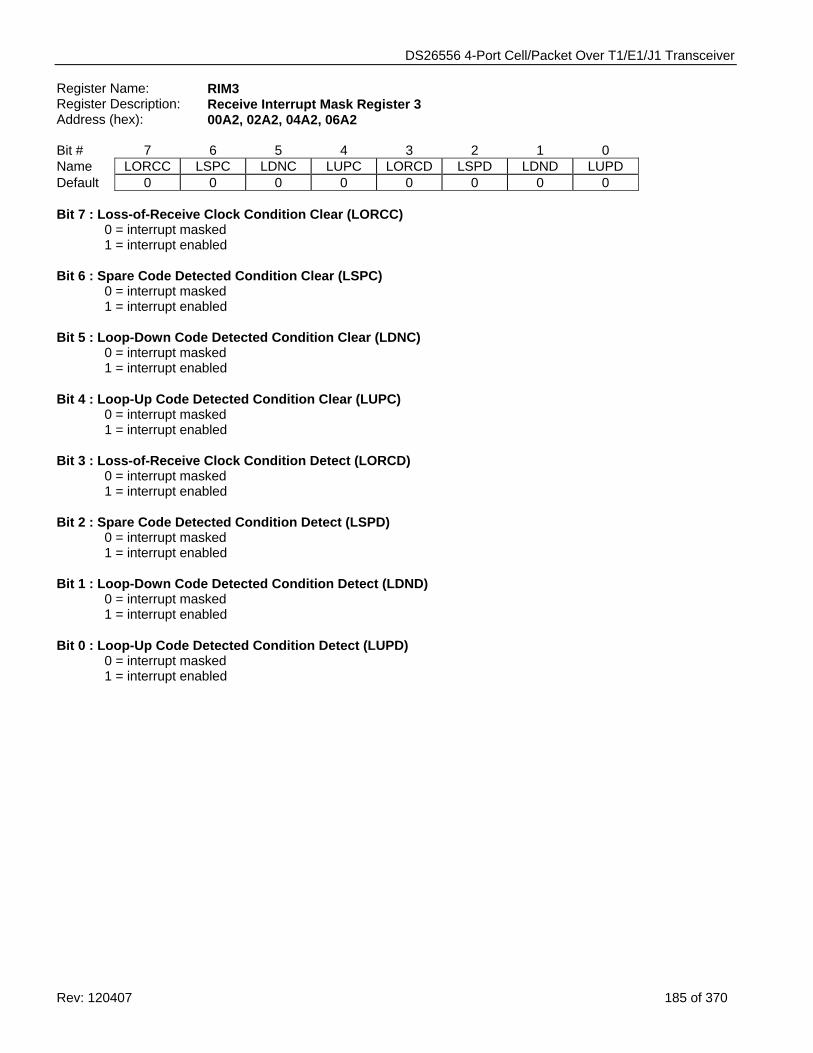
DS26556 4-Port Cell/Packet Over T1/E1/J1 Transceiver
Rev: 120407 185 of 370
Register Name: RIM3 Register Description: Receive Interrupt Mask Register 3 Address (hex): 00A2, 02A2, 04A2, 06A2 Bit # 7 6 5 4 3 2 1 0 Name LORCC LSPC LDNC LUPC LORCD LSPD LDND LUPD Default 0 0 0 0 0 0 0 0 Bit 7 : Loss-of-Receive Clock Condition Clear (LORCC)
0 = interrupt masked 1 = interrupt enabled
Bit 6 : Spare Code Detected Condition Clear (LSPC) 0 = interrupt masked 1 = interrupt enabled
Bit 5 : Loop-Down Code Detected Condition Clear (LDNC)
0 = interrupt masked 1 = interrupt enabled
Bit 4 : Loop-Up Code Detected Condition Clear (LUPC)
0 = interrupt masked 1 = interrupt enabled
Bit 3 : Loss-of-Receive Clock Condition Detect (LORCD)
0 = interrupt masked 1 = interrupt enabled
Bit 2 : Spare Code Detected Condition Detect (LSPD)
0 = interrupt masked 1 = interrupt enabled
Bit 1 : Loop-Down Code Detected Condition Detect (LDND)
0 = interrupt masked 1 = interrupt enabled
Bit 0 : Loop-Up Code Detected Condition Detect (LUPD)
0 = interrupt masked 1 = interrupt enabled
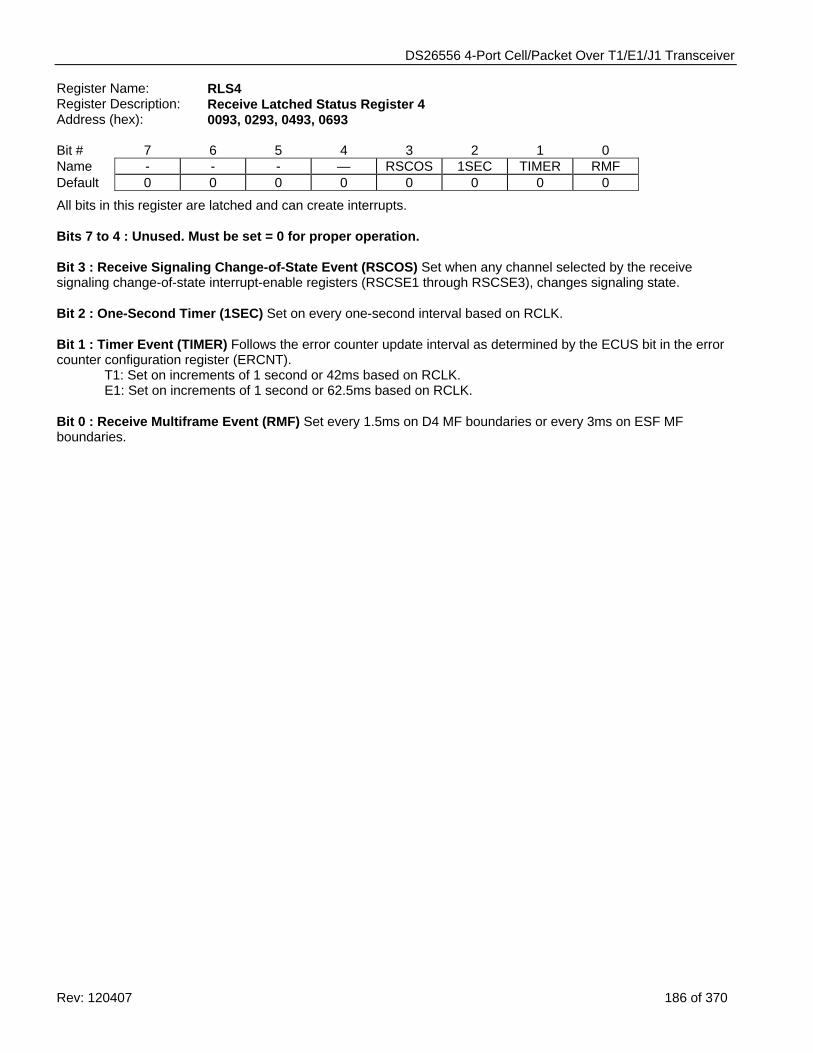
DS26556 4-Port Cell/Packet Over T1/E1/J1 Transceiver
Rev: 120407 186 of 370
Register Name: RLS4 Register Description: Receive Latched Status Register 4 Address (hex): 0093, 0293, 0493, 0693 Bit # 7 6 5 4 3 2 1 0 Name - - - — RSCOS 1SEC TIMER RMF Default 0 0 0 0 0 0 0 0
All bits in this register are latched and can create interrupts. Bits 7 to 4 : Unused. Must be set = 0 for proper operation. Bit 3 : Receive Signaling Change-of-State Event (RSCOS) Set when any channel selected by the receive signaling change-of-state interrupt-enable registers (RSCSE1 through RSCSE3), changes signaling state. Bit 2 : One-Second Timer (1SEC) Set on every one-second interval based on RCLK. Bit 1 : Timer Event (TIMER) Follows the error counter update interval as determined by the ECUS bit in the error counter configuration register (ERCNT).
T1: Set on increments of 1 second or 42ms based on RCLK. E1: Set on increments of 1 second or 62.5ms based on RCLK.
Bit 0 : Receive Multiframe Event (RMF) Set every 1.5ms on D4 MF boundaries or every 3ms on ESF MF boundaries.
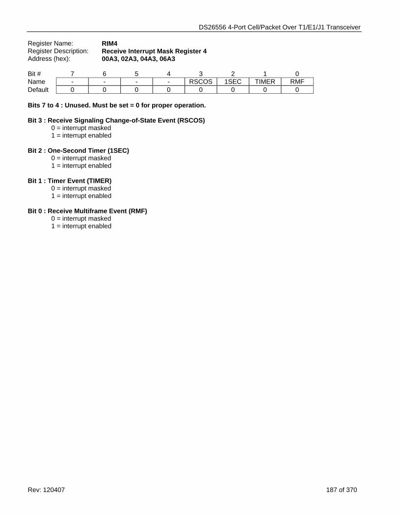
DS26556 4-Port Cell/Packet Over T1/E1/J1 Transceiver
Rev: 120407 187 of 370
Register Name: RIM4 Register Description: Receive Interrupt Mask Register 4 Address (hex): 00A3, 02A3, 04A3, 06A3 Bit # 7 6 5 4 3 2 1 0 Name - - - - RSCOS 1SEC TIMER RMF Default 0 0 0 0 0 0 0 0 Bits 7 to 4 : Unused. Must be set = 0 for proper operation. Bit 3 : Receive Signaling Change-of-State Event (RSCOS)
0 = interrupt masked 1 = interrupt enabled
Bit 2 : One-Second Timer (1SEC) 0 = interrupt masked 1 = interrupt enabled
Bit 1 : Timer Event (TIMER) 0 = interrupt masked 1 = interrupt enabled
Bit 0 : Receive Multiframe Event (RMF)
0 = interrupt masked 1 = interrupt enabled
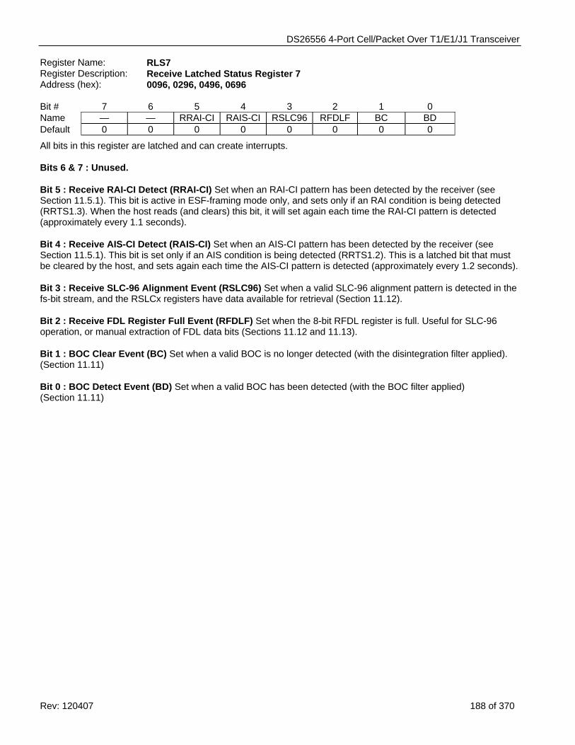
DS26556 4-Port Cell/Packet Over T1/E1/J1 Transceiver
Rev: 120407 188 of 370
Register Name: RLS7 Register Description: Receive Latched Status Register 7 Address (hex): 0096, 0296, 0496, 0696 Bit # 7 6 5 4 3 2 1 0 Name — — RRAI-CI RAIS-CI RSLC96 RFDLF BC BD Default 0 0 0 0 0 0 0 0
All bits in this register are latched and can create interrupts. Bits 6 & 7 : Unused. Bit 5 : Receive RAI-CI Detect (RRAI-CI) Set when an RAI-CI pattern has been detected by the receiver (see Section 11.5.1). This bit is active in ESF-framing mode only, and sets only if an RAI condition is being detected (RRTS1.3). When the host reads (and clears) this bit, it will set again each time the RAI-CI pattern is detected (approximately every 1.1 seconds). Bit 4 : Receive AIS-CI Detect (RAIS-CI) Set when an AIS-CI pattern has been detected by the receiver (see Section 11.5.1). This bit is set only if an AIS condition is being detected (RRTS1.2). This is a latched bit that must be cleared by the host, and sets again each time the AIS-CI pattern is detected (approximately every 1.2 seconds). Bit 3 : Receive SLC-96 Alignment Event (RSLC96) Set when a valid SLC-96 alignment pattern is detected in the fs-bit stream, and the RSLCx registers have data available for retrieval (Section 11.12). Bit 2 : Receive FDL Register Full Event (RFDLF) Set when the 8-bit RFDL register is full. Useful for SLC-96 operation, or manual extraction of FDL data bits (Sections 11.12 and 11.13). Bit 1 : BOC Clear Event (BC) Set when a valid BOC is no longer detected (with the disintegration filter applied). (Section 11.11) Bit 0 : BOC Detect Event (BD) Set when a valid BOC has been detected (with the BOC filter applied) (Section 11.11)
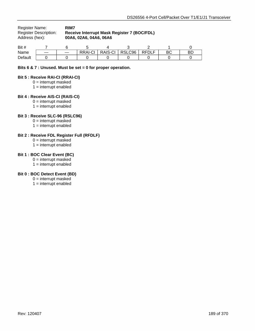
DS26556 4-Port Cell/Packet Over T1/E1/J1 Transceiver
Rev: 120407 189 of 370
Register Name: RIM7 Register Description: Receive Interrupt Mask Register 7 (BOC/FDL) Address (hex): 00A6, 02A6, 04A6, 06A6 Bit # 7 6 5 4 3 2 1 0 Name — — RRAI-CI RAIS-CI RSLC96 RFDLF BC BD Default 0 0 0 0 0 0 0 0 Bits 6 & 7 : Unused. Must be set = 0 for proper operation. Bit 5 : Receive RAI-CI (RRAI-CI)
0 = interrupt masked 1 = interrupt enabled
Bit 4 : Receive AIS-CI (RAIS-CI)
0 = interrupt masked 1 = interrupt enabled
Bit 3 : Receive SLC-96 (RSLC96)
0 = interrupt masked 1 = interrupt enabled
Bit 2 : Receive FDL Register Full (RFDLF)
0 = interrupt masked 1 = interrupt enabled
Bit 1 : BOC Clear Event (BC)
0 = interrupt masked 1 = interrupt enabled
Bit 0 : BOC Detect Event (BD)
0 = interrupt masked 1 = interrupt enabled
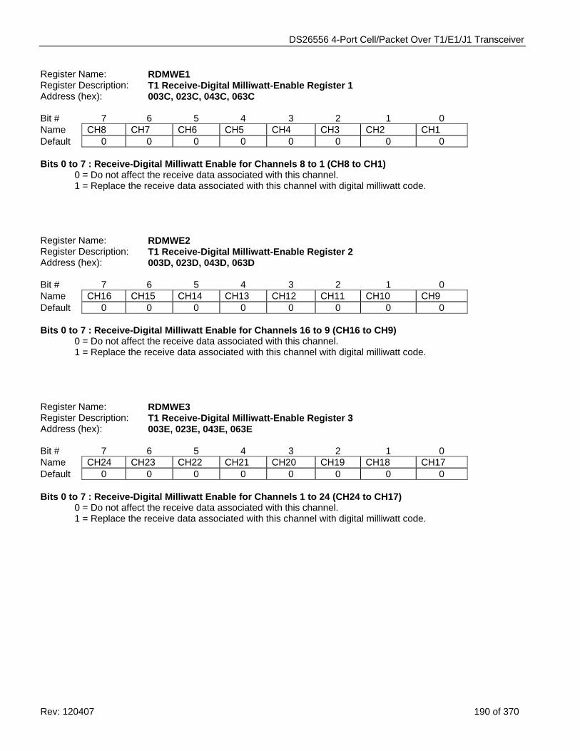
DS26556 4-Port Cell/Packet Over T1/E1/J1 Transceiver
Rev: 120407 190 of 370
Register Name: RDMWE1 Register Description: T1 Receive-Digital Milliwatt-Enable Register 1 Address (hex): 003C, 023C, 043C, 063C Bit # 7 6 5 4 3 2 1 0 Name CH8 CH7 CH6 CH5 CH4 CH3 CH2 CH1 Default 0 0 0 0 0 0 0 0 Bits 0 to 7 : Receive-Digital Milliwatt Enable for Channels 8 to 1 (CH8 to CH1)
0 = Do not affect the receive data associated with this channel. 1 = Replace the receive data associated with this channel with digital milliwatt code.
Register Name: RDMWE2 Register Description: T1 Receive-Digital Milliwatt-Enable Register 2 Address (hex): 003D, 023D, 043D, 063D Bit # 7 6 5 4 3 2 1 0 Name CH16 CH15 CH14 CH13 CH12 CH11 CH10 CH9 Default 0 0 0 0 0 0 0 0 Bits 0 to 7 : Receive-Digital Milliwatt Enable for Channels 16 to 9 (CH16 to CH9)
0 = Do not affect the receive data associated with this channel. 1 = Replace the receive data associated with this channel with digital milliwatt code.
Register Name: RDMWE3 Register Description: T1 Receive-Digital Milliwatt-Enable Register 3 Address (hex): 003E, 023E, 043E, 063E Bit # 7 6 5 4 3 2 1 0 Name CH24 CH23 CH22 CH21 CH20 CH19 CH18 CH17 Default 0 0 0 0 0 0 0 0 Bits 0 to 7 : Receive-Digital Milliwatt Enable for Channels 1 to 24 (CH24 to CH17)
0 = Do not affect the receive data associated with this channel. 1 = Replace the receive data associated with this channel with digital milliwatt code.
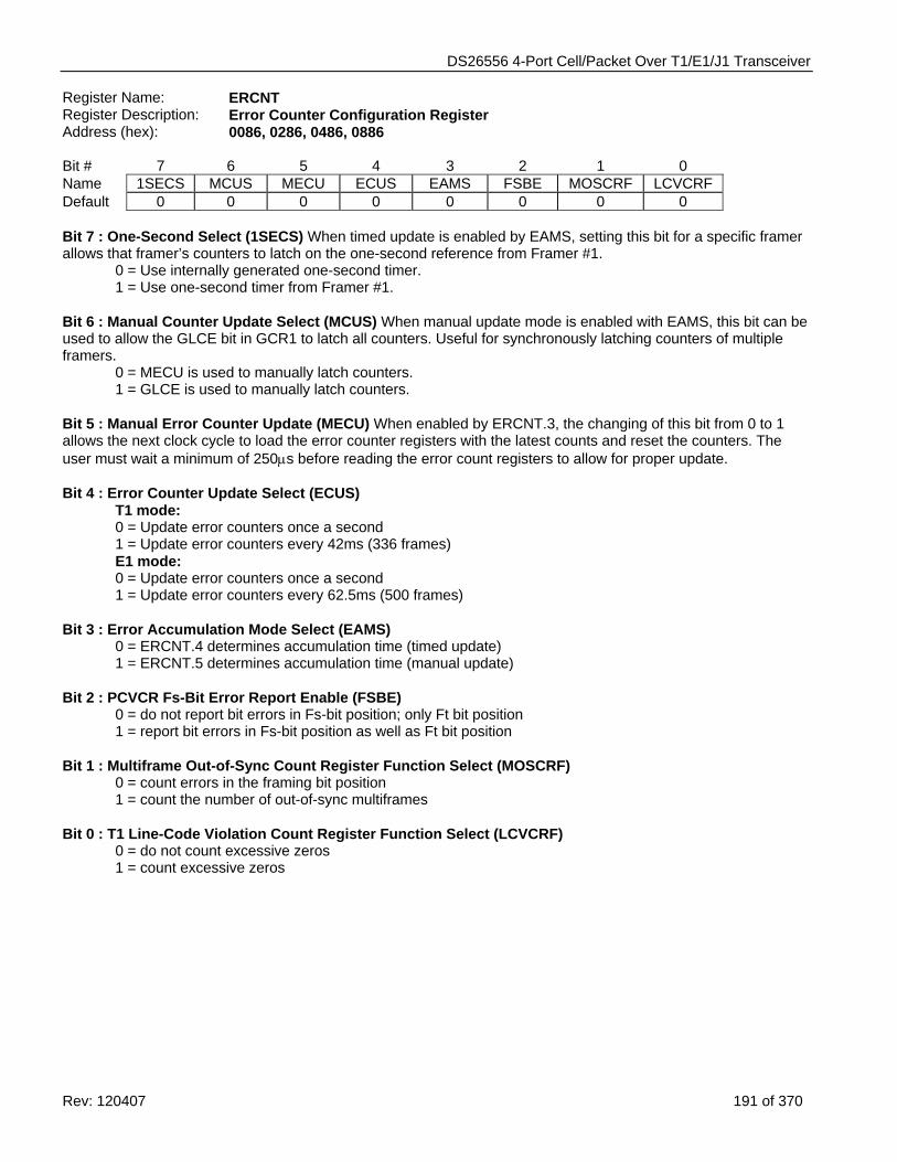
DS26556 4-Port Cell/Packet Over T1/E1/J1 Transceiver
Rev: 120407 191 of 370
Register Name: ERCNT Register Description: Error Counter Configuration Register Address (hex): 0086, 0286, 0486, 0886 Bit # 7 6 5 4 3 2 1 0 Name 1SECS MCUS MECU ECUS EAMS FSBE MOSCRF LCVCRF Default 0 0 0 0 0 0 0 0
Bit 7 : One-Second Select (1SECS) When timed update is enabled by EAMS, setting this bit for a specific framer allows that framer’s counters to latch on the one-second reference from Framer #1.
0 = Use internally generated one-second timer. 1 = Use one-second timer from Framer #1. Bit 6 : Manual Counter Update Select (MCUS) When manual update mode is enabled with EAMS, this bit can be used to allow the GLCE bit in GCR1 to latch all counters. Useful for synchronously latching counters of multiple framers.
0 = MECU is used to manually latch counters. 1 = GLCE is used to manually latch counters. Bit 5 : Manual Error Counter Update (MECU) When enabled by ERCNT.3, the changing of this bit from 0 to 1 allows the next clock cycle to load the error counter registers with the latest counts and reset the counters. The user must wait a minimum of 250μs before reading the error count registers to allow for proper update. Bit 4 : Error Counter Update Select (ECUS)
T1 mode: 0 = Update error counters once a second 1 = Update error counters every 42ms (336 frames) E1 mode: 0 = Update error counters once a second 1 = Update error counters every 62.5ms (500 frames)
Bit 3 : Error Accumulation Mode Select (EAMS)
0 = ERCNT.4 determines accumulation time (timed update) 1 = ERCNT.5 determines accumulation time (manual update)
Bit 2 : PCVCR Fs-Bit Error Report Enable (FSBE)
0 = do not report bit errors in Fs-bit position; only Ft bit position 1 = report bit errors in Fs-bit position as well as Ft bit position
Bit 1 : Multiframe Out-of-Sync Count Register Function Select (MOSCRF)
0 = count errors in the framing bit position 1 = count the number of out-of-sync multiframes
Bit 0 : T1 Line-Code Violation Count Register Function Select (LCVCRF)
0 = do not count excessive zeros 1 = count excessive zeros
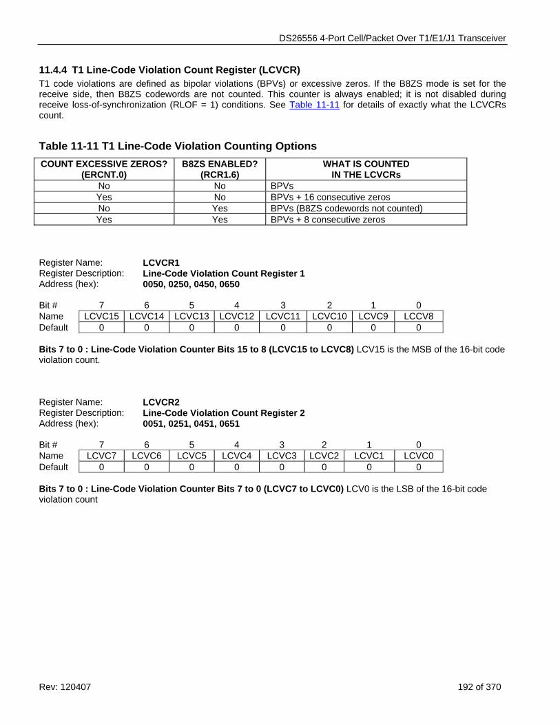
DS26556 4-Port Cell/Packet Over T1/E1/J1 Transceiver
Rev: 120407 192 of 370
11.4.4 T1 Line-Code Violation Count Register (LCVCR) T1 code violations are defined as bipolar violations (BPVs) or excessive zeros. If the B8ZS mode is set for the receive side, then B8ZS codewords are not counted. This counter is always enabled; it is not disabled during receive loss-of-synchronization (RLOF = 1) conditions. See Table 11-11 for details of exactly what the LCVCRs count.
Table 11-11 T1 Line-Code Violation Counting Options COUNT EXCESSIVE ZEROS?
(ERCNT.0) B8ZS ENABLED?
(RCR1.6) WHAT IS COUNTED
IN THE LCVCRs No No BPVs Yes No BPVs + 16 consecutive zeros No Yes BPVs (B8ZS codewords not counted) Yes Yes BPVs + 8 consecutive zeros
Register Name: LCVCR1 Register Description: Line-Code Violation Count Register 1 Address (hex): 0050, 0250, 0450, 0650 Bit # 7 6 5 4 3 2 1 0 Name LCVC15 LCVC14 LCVC13 LCVC12 LCVC11 LCVC10 LCVC9 LCCV8 Default 0 0 0 0 0 0 0 0 Bits 7 to 0 : Line-Code Violation Counter Bits 15 to 8 (LCVC15 to LCVC8) LCV15 is the MSB of the 16-bit code violation count. Register Name: LCVCR2 Register Description: Line-Code Violation Count Register 2 Address (hex): 0051, 0251, 0451, 0651 Bit # 7 6 5 4 3 2 1 0 Name LCVC7 LCVC6 LCVC5 LCVC4 LCVC3 LCVC2 LCVC1 LCVC0 Default 0 0 0 0 0 0 0 0 Bits 7 to 0 : Line-Code Violation Counter Bits 7 to 0 (LCVC7 to LCVC0) LCV0 is the LSB of the 16-bit code violation count
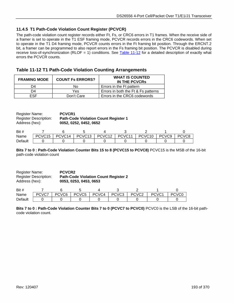
DS26556 4-Port Cell/Packet Over T1/E1/J1 Transceiver
Rev: 120407 193 of 370
11.4.5 T1 Path-Code Violation Count Register (PCVCR) The path-code violation count register records either Ft, Fs, or CRC6 errors in T1 frames. When the receive side of a framer is set to operate in the T1 ESF framing mode, PCVCR records errors in the CRC6 codewords. When set to operate in the T1 D4 framing mode, PCVCR counts errors in the Ft framing bit position. Through the ERCNT.2 bit, a framer can be programmed to also report errors in the Fs framing bit position. The PCVCR is disabled during receive loss-of-synchronization (RLOF = 1) conditions. See Table 11-12 for a detailed description of exactly what errors the PCVCR counts.
Table 11-12 T1 Path-Code Violation Counting Arrangements
FRAMING MODE COUNT Fs ERRORS? WHAT IS COUNTED IN THE PCVCRs
D4 No Errors in the Ft pattern D4 Yes Errors in both the Ft & Fs patterns
ESF Don’t Care Errors in the CRC6 codewords Register Name: PCVCR1 Register Description: Path-Code Violation Count Register 1 Address (hex): 0052, 0252, 0452, 0652 Bit # 7 6 5 4 3 2 1 0 Name PCVC15 PCVC14 PCVC13 PCVC12 PCVC11 PCVC10 PCVC9 PCVC8 Default 0 0 0 0 0 0 0 0 Bits 7 to 0 : Path-Code Violation Counter Bits 15 to 8 (PCVC15 to PCVC8) PCVC15 is the MSB of the 16-bit path-code violation count Register Name: PCVCR2 Register Description: Path-Code Violation Count Register 2 Address (hex): 0053, 0253, 0453, 0653 Bit # 7 6 5 4 3 2 1 0 Name PCVC7 PCVC6 PCVC5 PCVC4 PCVC3 PCVC2 PCVC1 PCVC0 Default 0 0 0 0 0 0 0 0 Bits 7 to 0 : Path-Code Violation Counter Bits 7 to 0 (PCVC7 to PCVC0) PCVC0 is the LSB of the 16-bit path-code violation count.
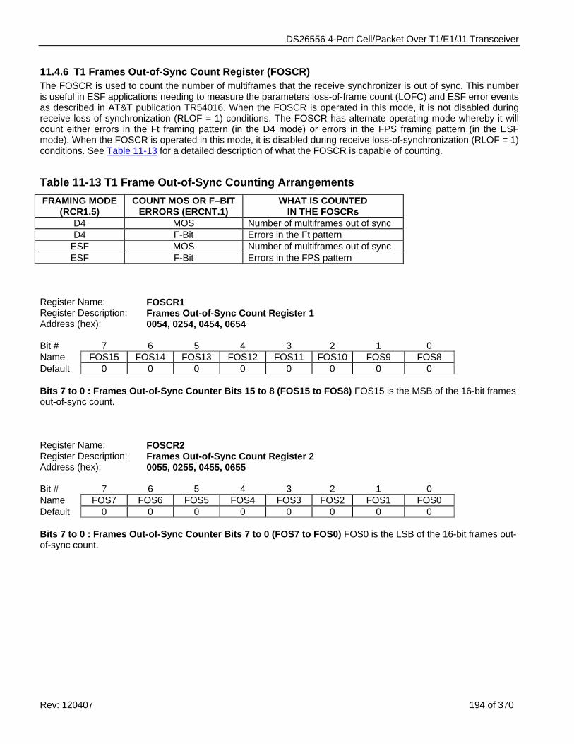
DS26556 4-Port Cell/Packet Over T1/E1/J1 Transceiver
Rev: 120407 194 of 370
11.4.6 T1 Frames Out-of-Sync Count Register (FOSCR) The FOSCR is used to count the number of multiframes that the receive synchronizer is out of sync. This number is useful in ESF applications needing to measure the parameters loss-of-frame count (LOFC) and ESF error events as described in AT&T publication TR54016. When the FOSCR is operated in this mode, it is not disabled during receive loss of synchronization (RLOF = 1) conditions. The FOSCR has alternate operating mode whereby it will count either errors in the Ft framing pattern (in the D4 mode) or errors in the FPS framing pattern (in the ESF mode). When the FOSCR is operated in this mode, it is disabled during receive loss-of-synchronization (RLOF = 1) conditions. See Table 11-13 for a detailed description of what the FOSCR is capable of counting.
Table 11-13 T1 Frame Out-of-Sync Counting Arrangements FRAMING MODE
(RCR1.5) COUNT MOS OR F–BIT
ERRORS (ERCNT.1) WHAT IS COUNTED
IN THE FOSCRs D4 MOS Number of multiframes out of sync D4 F-Bit Errors in the Ft pattern
ESF MOS Number of multiframes out of sync ESF F-Bit Errors in the FPS pattern
Register Name: FOSCR1 Register Description: Frames Out-of-Sync Count Register 1 Address (hex): 0054, 0254, 0454, 0654 Bit # 7 6 5 4 3 2 1 0 Name FOS15 FOS14 FOS13 FOS12 FOS11 FOS10 FOS9 FOS8 Default 0 0 0 0 0 0 0 0 Bits 7 to 0 : Frames Out-of-Sync Counter Bits 15 to 8 (FOS15 to FOS8) FOS15 is the MSB of the 16-bit frames out-of-sync count. Register Name: FOSCR2 Register Description: Frames Out-of-Sync Count Register 2 Address (hex): 0055, 0255, 0455, 0655 Bit # 7 6 5 4 3 2 1 0 Name FOS7 FOS6 FOS5 FOS4 FOS3 FOS2 FOS1 FOS0 Default 0 0 0 0 0 0 0 0 Bits 7 to 0 : Frames Out-of-Sync Counter Bits 7 to 0 (FOS7 to FOS0) FOS0 is the LSB of the 16-bit frames out-of-sync count.
DS26556 4-Port Cell/Packet Over T1/E1/J1 Transceiver
Rev: 120407 195 of 370
11.4.7 DS0 Monitoring Function The DS26556 can monitor one DS0 (64kbps) channel in the transmit direction and one DS0 channel in the receive direction at the same time. In the receive direction, the RCM0 to RCM4 bits in the RDS0SEL register need to be properly set and the DS0 channel pointed to by the RCM0 to RCM4 bits will appear in the receive DS0 (RDS0M) register. The RCM4 to RCM0 bits should be programmed with the decimal decode of the appropriate T1 channel. T1 channels 1 through 24 map to register values 0 through 23. For example, if DS0 channel 15 in the receive direction needed to be monitored, then the following values would be programmed into RDS0SEL:
RCM4 = 0 RCM3 = 1 RCM2 = 1 RCM1 = 1 RCM0 = 0
Register Name: RDS0SEL Register Description: Receive-Channel Monitor Select Address (hex): 0012, 0212, 0412, 0612 Bit # 7 6 5 4 3 2 1 0 Name — — — RCM4 RCM3 RCM2 RCM1 RCM0 Default 0 0 0 0 0 0 0 0 Bits 7 to 5 : Unused. Must be set = 0 for proper operation. Bits 4 to 0 : Receive-Channel Monitor Bits (RCM4 to RCM0) RCM0 is the LSB of a 5-bit channel select that determines which receive-DS0 channel data appears in the RDS0M register. Register Name: RDS0M Register Description: Receive-DS0 Monitor Register Address (hex): 0060, 0260, 0460, 0660 Bit # 7 6 5 4 3 2 1 0 Name B1 B2 B3 B4 B5 B6 B7 B8 Default 0 0 0 0 0 0 0 0 Bits 7 to 0 : Receive-DS0 Channel Bits (B1 to B8) Receive-channel data that has been selected by the receive-channel monitor select register. B8 is the LSB of the DS0 channel (last bit to be received).
DS26556 4-Port Cell/Packet Over T1/E1/J1 Transceiver
Rev: 120407 196 of 370
11.4.8 Receive Signaling Registers Register Name: RSIGC Register Description: Receive Signaling Control Register Address (hex): 0013, 0213, 0413, 0613 Bit # 7 6 5 4 3 2 1 0 Name — — — RFSA1 — RSFF RSFE RSIE Default 0 0 0 0 0 0 0 0 Bits 7 to 5 : Unused. Must be set = 0 for proper operation. Bit 4 : Receive-Force Signaling All Ones (RFSA1) 0 = do not force robbed bit signaling to all ones
1 = force signaling bits to all ones on a per-channel basis according to the RSAOI1–RSAOI3 registers
Bit 3 : Unused. Must be set = 0 for proper operation. Bit 2 : Receive-Signaling Force Freeze (RSFF). Freezes receive-side signaling at RSIG (and RSER if receive-signaling reinsertion is enabled); overrides receive-freeze enable (RFE).
0 = do not force a freeze event 1 = force a freeze event
Bit 1 : Receive-Signaling Freeze Enable (RSFE)
0 = no freezing of receive-signaling data occurs 1 = allow freezing of receive-signaling data at RSIG (and RSER if receive-signaling reinsertion is enabled)
Bit 0 : Receive-Signaling Integration Enable (RSIE) 0 = signaling changes of state reported on any change in selected channels 1 = signaling must be stable for three multiframes for a change of state to be reported
DS26556 4-Port Cell/Packet Over T1/E1/J1 Transceiver
Rev: 120407 197 of 370
Register Name: RSI1, RSI2, RSI3, RSI4 Register Description: Receive-Signaling Reinsertion Enable Registers Address (hex): 00C8, 02C8, 04C8, 06C8 Setting any of the CH1 through CH24 bits in the RSI1 through RSI3 registers causes signaling data to be reinserted for the associated channel. RSI4 is used for 2.048MHz backplane operation. (MSB) (LSB) CH8 CH7 CH6 CH5 CH4 CH3 CH2 CH1 RSI1 CH16 CH15 CH14 CH13 CH12 CH11 CH10 CH9 RSI2 CH24 CH23 CH22 CH21 CH20 CH19 CH18 CH17 RSI3 CH32 CH31 CH30 CH29 CH28 CH27 CH26 CH25 RSI4*
Register Name: RSAOI1, RSAOI2, RSAOI3, Register Description: Receive-Signaling All-Ones Insertion Registers Address (hex): 0038 to 003A, 0238 to 023A, 0438 to 043A, 0638 to 063A Setting any of the CH1 through CH24 bits in the RSAOI1 through RSAOI3 registers causes signaling data to be replaced with logic ones as received at the backplane. (MSB) (LSB) CH8 CH7 CH6 CH5 CH4 CH3 CH2 CH1 RSAOI1 CH16 CH15 CH14 CH13 CH12 CH11 CH10 CH9 RSAOI2 CH24 CH23 CH22 CH21 CH20 CH19 CH18 CH17 RSAOI3
DS26556 4-Port Cell/Packet Over T1/E1/J1 Transceiver
Rev: 120407 198 of 370
Register Name: RS1 to RS12 Register Description: Receive Signaling Registers Address (hex): 0040 to 004B, 0240 to 024B, 0440 to 044B, 0640 to 064B In the ESF framing mode, there can be up to four signaling bits per channel (A, B, C, and D). In the D4 framing mode, there are only two signaling bits per channel (A and B). In the D4 framing mode, the framer repeats the A and B signaling data in the C and D bit locations. Therefore, when the framer is operated in D4 framing mode, the user needs to retrieve the signaling bits every 1.5ms as opposed to 3ms for ESF mode. The receive-signaling registers are frozen and not updated during a loss-of-sync condition. They contain the most recent signaling information before the OOF occurred. (MSB) (LSB) CH1-A CH1-B CH1-C CH1-D CH13-A CH13-B CH13-C CH13-D RS1 CH2-A CH2-B CH2-C CH2-D CH14-A CH14-B CH14-C CH14-D RS2 CH3-A CH3-B CH3-C CH3-D CH15-A CH15-B CH15-C CH15-D RS3 CH4-A CH4-B CH4-C CH4-D CH16-A CH16-B CH16-C CH16-D RS4 CH5-A CH5-B CH5-C CH5-D CH17-A CH17-B CH17-C CH17-D RS5 CH6-A CH6-B CH6-C CH6-D CH18-A CH18-B CH18-C CH18-D RS6 CH7-A CH7-B CH7-C CH7-D CH19-A CH19-B CH19-C CH19-D RS7 CH8-A CH8-B CH8-C CH8-D CH20-A CH20-B CH20-C CH20-D RS8 CH9-A CH9-B CH9-C CH9-D CH21-A CH21-B CH21-C CH21-D RS9
CH10-A CH10-B CH10-C CH10-D CH22-A CH22-B CH22-C CH22-D RS10 CH11-A CH11-B CH11-C CH11-D CH23-A CH23-B CH23-C CH23-D RS11 CH12-A CH12-B CH12-C CH12-D CH24-A CH24-B CH24-C CH24-D RS12
DS26556 4-Port Cell/Packet Over T1/E1/J1 Transceiver
Rev: 120407 199 of 370
Register Name: RSS1, RSS2, RSS3 Register Description: Receive Signaling Status Registers Address (hex): 0098 to 009A, 0298 to 029A, 0498, to 049A When a channel’s signaling data changes state, the respective bit in registers RSS1–RSS3 is set and latched. The RSCOS bit (RLSR4.3) is set if the channel was also enabled by setting the appropriate bit in RSCSE1–3. The INT signal goes low if enabled by the interrupt mask bit RIM4.3. Bit # 7 6 5 4 3 2 1 0 Name CH8 CH7 CH6 CH5 CH4 CH3 CH2 CH1 RSS1 Name CH16 CH15 CH14 CH13 CH12 CH11 CH10 CH9 RSS2 Name CH24 CH23 CH22 CH21 CH20 CH19 CH18 CH17 RSS3 Default 0 0 0 0 0 0 0 0
Note: Status bits in this register are latched. Register Name: RSCSE1, RSCSE2, RSCSE3 Register Description: Receive-Signaling Change-of-State Enable Address (hex): 00A8 to 00AA, 02A8 to 02AA, 04A8, to 04AA Setting any of the CH1 through CH24 bits in the RSS1 through RSS3 registers cause RSCOS (RLSR4.3) to be set when that channel’s signaling data changes state. Bit # 7 6 5 4 3 2 1 0 Name CH8 CH7 CH6 CH5 CH4 CH3 CH2 CH1 RSCSE1 Name CH16 CH15 CH14 CH13 CH12 CH11 CH10 CH9 RSCSE2 Name CH24 CH23 CH22 CH21 CH20 CH19 CH18 CH17 RSCSE3 Default 0 0 0 0 0 0 0 0
11.4.9 T1 Receive Per-Channel Idle Code Insertion Channel data can be replaced by an idle code on a per-channel basis in the transmit and receive directions. Twenty-four receive idle definition registers (RIDR1–RIDR24) are provided to set the 8-bit idle code for each channel. The receive-channel idle code-enable registers (RCICE1–3) are used to enable idle code replacement on a per-channel basis. The receive-channel idle code-enable registers (RCICE1/2/3) are used to determine which of the 24 T1 channels from the T1 line to the backplane should be overwritten with the code placed in the receive idle-code definition register. Register Name: RIDR1 to RIDR24 Register Description: Receive Idle-Code Definition Registers 1 to 24 Address (hex): 0020 to 0037, 0220 to 0237, 0420 to 0437, 0620 to 0637 Bit # 7 6 5 4 3 2 1 0 Name C7 C6 C5 C4 C3 C2 C1 C0 Default 0 0 0 0 0 0 0 0 Bits 7 to 0 : Per-Channel Idle Code Bits (C7 to C0) C0 is the LSB of the code (this bit is transmitted last). Address 20H is for channel 1; address 37H is for channel 24.
DS26556 4-Port Cell/Packet Over T1/E1/J1 Transceiver
Rev: 120407 200 of 370
Register Name: RCICE1, RCICE2, RCICE3 Register Description: Receive-Channel Idle Code-Enable Registers Address (hex): 00D0 to 00D2, 02D0 to 02D2, 04D0 to 04D2, 06D0 t0 06D2
Bit # 7 6 5 4 3 2 1 0 Name CH8 CH7 CH6 CH5 CH4 CH3 CH2 CH1 RCICE1 Name CH16 CH15 CH14 CH13 CH12 CH11 CH10 CH9 RCICE2 Name CH24 CH23 CH22 CH21 CH20 CH19 CH18 CH17 RCICE3 Default 0 0 0 0 0 0 0 0
Bits 7 to 0 : Receive Channels 24 to 1 Code Insertion Control Bits (CH24 to CH1)
0 = do not insert data from the idle code array into the receive data stream 1 = insert data from the idle code array into the receive data stream
11.4.10 T1 Receive Channel Mark Registers The Receive Channel Mark Registers (RCMR1/RCMR2/RCMR3/RCMR4) control the mapping of channels to the receive cell/packet interface and the RCHMRK pin. The RCHMRK signal is used internally to select which channels will be mapped to the receive cell/packet interface. Externally, the signal can be used to multiplex TDM data out of channels not used by the receive cell/packet interface. When the appropriate bits are set to 1, the receive cell/packet function is mapped to that channel and externally the RCHMRK pin is held high during the entire corresponding channel time. In T1 mode, only RCMR1 to RCMR3 and the LSB of RCMR4 are used. Register Name: RCMR1, RCMR2, RCMR3 Register Description: Receive-Channel Mark Registers 1 to 3 Address (hex): 00C4 to 00C6, 02C4 to 02C6, 04C4 to 04C6, 06C4 to 06C6 (MSB) (LSB) CH8 CH7 CH6 CH5 CH4 CH3 CH2 CH1 RCMR1 CH16 CH15 CH14 CH13 CH12 CH11 CH10 CH9 RCMR2 CH24 CH23 CH22 CH21 CH20 CH19 CH18 CH17 RCMR3
Bits 7 to 0 : Receive Channels 24 to 1 Channel Mark Control Bits (CH24 to CH1)
0 = force the RCHMRK pin to remain low during this channel time 1 = force the RCHMRK pin high during this channel time
Register Name: RCMR4 Register Description: Receive-Channel Mark Register 4 Address (hex): 00C7, 02C7, 04C7, 06C7 (MSB) (LSB)
RFBIT RCMR4 Bits 7 to 1 : Unused. Must be set = 0 for proper operation. Bit 0 : Receive F Bit (RFBIT)
RCMR4.0 = 0, RCHMRK low during the F-bit RCMR4.0 = 1, RCHMRK high during the F-bit
DS26556 4-Port Cell/Packet Over T1/E1/J1 Transceiver
Rev: 120407 201 of 370
Register Name: RGCCR Register Description: Receive Gapped Clock Control Register Address (hex): 0085, 0285, 0485, 0685 Bit # 7 6 5 4 3 2 1 0 Name RCCF RGCE - - - - - - Default 0 0 0 0 0 0 0 0 Bit 7 : Receive Channel Clock Format (RCCF) This bit controls the function of the RCHMRK pin went it is in the channel clock mode and the RGCCR.6 bit is set = 1. Channel clock mode is enabled in the RCHMRK Pin Function Select (RPFS) register.
0 = 64kbps, clock output during all 8 bits 1 = 56kbps, clock output during 7 MSBs
Bit 6 :/ Receive Gapped Clock Enable (RGCE) This bit controls the function of the RCHMRK pin went it is in the channel clock mode. Channel clock mode is enabled in the RCHMRK Pin Function Select (RPFS) register.
0 = RCHMRK outputs a pulse during the LSB of each channel time. 1 = RCHMRK outputs a gapped bit clock as selected by the RGCCS1 through RGCCC4 registers.
Bits 5 to 0 : Unused. Must be set = 0 for proper operation.
11.4.11 Receive Fractional T1 Support (Gapped-Clock Mode) Register Name: RGCCS1, RGCCS2, RGCCS3, RGCCS4 Register Description: Receive-Gapped-Clock Channel-Select Registers Address (hex): 00CC to 00CF, 02CC to 02CF, 04CC to 04CF, 06CC to 06CF (MSB) (LSB) CH8 CH7 CH6 CH5 CH4 CH3 CH2 CH1 RGCCS1 CH16 CH15 CH14 CH13 CH12 CH11 CH10 CH9 RGCCS2 CH24 CH23 CH22 CH21 CH20 CH19 CH18 CH17 RGCCS3 CH32 CH31 CH30 CH29 CH28 CH27 CH26 CH25/F-Bit RGCCS4*
Bits 7 to 0 : Receive Channels 1 to 32 Gapped-Clock Channel Select Bits (CH1 to CH32) These bits control the RCHMRK pin when it is in the channel clock mode. Channel clock mode is enabled in the RCHMRK Pin Function Select (RPFS) register.
0 = no clock is present on RCHMRK during this channel time 1 = force a clock on RCHMRK during this channel time. The clock will be synchronous with RCLK.
Note that RGCCS4 has two functions:
When 2.048MHz backplane mode is selected, this register allows the user to enable the gapped clock on RCHMRK for any of the 32 possible backplane channels. When 1.544MHz backplane mode is selected, the LSB of this register determines whether or not a clock is generated on RCHMRK during the F-bit time: RGCCS4.0 = 0: do not generate a clock during the F-bit RGCCS4.0 = 1: generate a clock during the F-bit In this mode, RGCCS4.1—RGCCS4.7 should be set to 0.
DS26556 4-Port Cell/Packet Over T1/E1/J1 Transceiver
Rev: 120407 202 of 370
11.4.12 Receive T1 Bit-Oriented Code (BOC) Controller Register Name: RBOCC Register Description: Receive BOC Control Register Address (hex): 0015, 0215, 0415, 0615 Bit # 7 6 5 4 3 2 1 0 Name RBR — RBD1 RBD0 — RBF1 RBF0 — Default 0 0 0 0 0 0 0 0 Bit 7 :Receive-BOC Reset (RBR) A 0-to-1 transition resets the BOC circuitry. Must be cleared and set again for a subsequent reset. Modifications to the RBF0, RBF1, RBD0, and RBD1 bits are not applied to the BOC controller until a BOC reset has been completed. Bit 6 : Unused. Must be set = 0 for proper operation. Bits 5 to 4 : Receive-BOC-Disintegration Bits (RBD0, RBD1) The BOC Disintegration filter sets the number of message bits that must be received without a valid BOC in order to set the BC bit indicating that a valid BOC is no longer being received.
RBD1 RBD0 Consecutive Message Bits for BOC Clear Identification 0 0 16 0 1 32 1 0 48 1 1 64 (Note 1)
Bit 3 : Unused. Must be set = 0 for proper operation. Bits 2 to 1 : Receive-BOC-Filter Bits (RBF0, RBF1) The BOC filter sets the number of consecutive patterns that must be received without error prior to an indication of a valid message.
RBF1 RBF0 Consecutive BOC Codes for Valid Sequence Identification 0 0 None 0 1 3 1 0 5 1 1 7 (Note 1)
Bit 0 : Unused. Must be set = 0 for proper operation. Note 1: The DS26556’s BOC controller does not integrate and disintegrate concurrently. Therefore, if the maximum integration time and the maximum disintegration time are used together, BOC messages that repeat fewer than 11 times may not be detected.
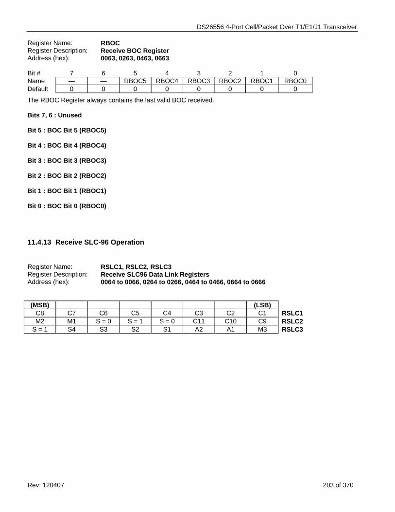
DS26556 4-Port Cell/Packet Over T1/E1/J1 Transceiver
Rev: 120407 203 of 370
Register Name: RBOC Register Description: Receive BOC Register Address (hex): 0063, 0263, 0463, 0663 Bit # 7 6 5 4 3 2 1 0 Name — — RBOC5 RBOC4 RBOC3 RBOC2 RBOC1 RBOC0 Default 0 0 0 0 0 0 0 0
The RBOC Register always contains the last valid BOC received. Bits 7, 6 : Unused Bit 5 : BOC Bit 5 (RBOC5) Bit 4 : BOC Bit 4 (RBOC4) Bit 3 : BOC Bit 3 (RBOC3) Bit 2 : BOC Bit 2 (RBOC2) Bit 1 : BOC Bit 1 (RBOC1) Bit 0 : BOC Bit 0 (RBOC0)
11.4.13 Receive SLC-96 Operation Register Name: RSLC1, RSLC2, RSLC3 Register Description: Receive SLC96 Data Link Registers Address (hex): 0064 to 0066, 0264 to 0266, 0464 to 0466, 0664 to 0666 (MSB) (LSB)
C8 C7 C6 C5 C4 C3 C2 C1 RSLC1 M2 M1 S = 0 S = 1 S = 0 C11 C10 C9 RSLC2
S = 1 S4 S3 S2 S1 A2 A1 M3 RSLC3
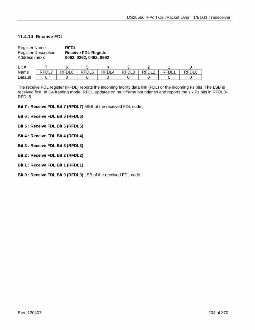
DS26556 4-Port Cell/Packet Over T1/E1/J1 Transceiver
Rev: 120407 204 of 370
11.4.14 Receive FDL Register Name: RFDL Register Description: Receive FDL Register Address (hex): 0062, 0262, 0462, 0662 Bit # 7 6 5 4 3 2 1 0 Name RFDL7 RFDL6 RFDL5 RFDL4 RFDL3 RFDL2 RFDL1 RFDL0 Default 0 0 0 0 0 0 0 0 The receive FDL register (RFDL) reports the incoming facility data link (FDL) or the incoming Fs bits. The LSB is received first. In D4 framing mode, RFDL updates on multiframe boundaries and reports the six Fs bits in RFDL0–RFDL5. Bit 7 : Receive FDL Bit 7 (RFDL7) MSB of the received FDL code. Bit 6 : Receive FDL Bit 6 (RFDL6) Bit 5 : Receive FDL Bit 5 (RFDL5) Bit 4 : Receive FDL Bit 4 (RFDL4) Bit 3 : Receive FDL Bit 3 (RFDL3) Bit 2 : Receive FDL Bit 2 (RFDL2) Bit 1 : Receive FDL Bit 1 (RFDL1) Bit 0 : Receive FDL Bit 0 (RFDL0) LSB of the received FDL code.
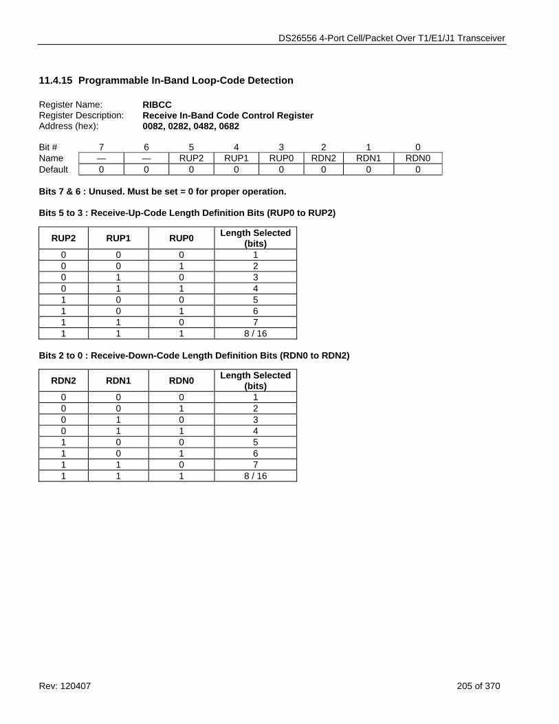
DS26556 4-Port Cell/Packet Over T1/E1/J1 Transceiver
Rev: 120407 205 of 370
11.4.15 Programmable In-Band Loop-Code Detection Register Name: RIBCC Register Description: Receive In-Band Code Control Register Address (hex): 0082, 0282, 0482, 0682 Bit # 7 6 5 4 3 2 1 0 Name — — RUP2 RUP1 RUP0 RDN2 RDN1 RDN0 Default 0 0 0 0 0 0 0 0 Bits 7 & 6 : Unused. Must be set = 0 for proper operation. Bits 5 to 3 : Receive-Up-Code Length Definition Bits (RUP0 to RUP2)
RUP2 RUP1 RUP0 Length Selected (bits)
0 0 0 1 0 0 1 2 0 1 0 3 0 1 1 4 1 0 0 5 1 0 1 6 1 1 0 7 1 1 1 8 / 16
Bits 2 to 0 : Receive-Down-Code Length Definition Bits (RDN0 to RDN2)
RDN2 RDN1 RDN0 Length Selected (bits)
0 0 0 1 0 0 1 2 0 1 0 3 0 1 1 4 1 0 0 5 1 0 1 6 1 1 0 7 1 1 1 8 / 16
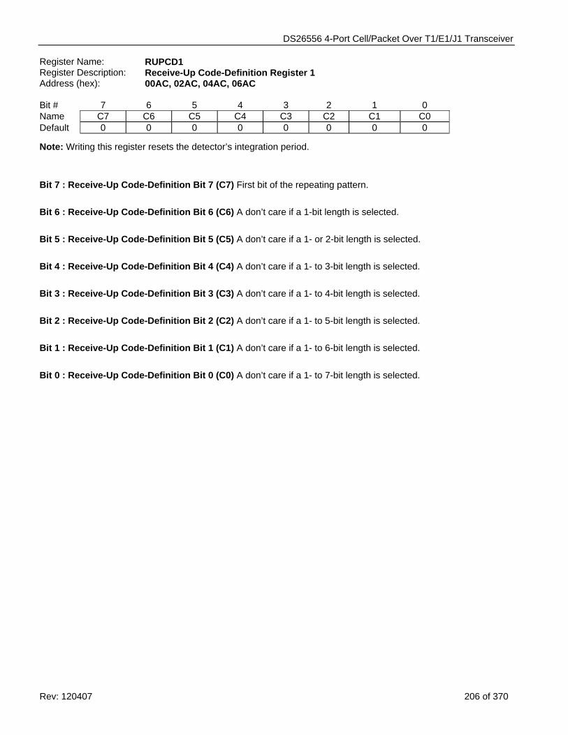
DS26556 4-Port Cell/Packet Over T1/E1/J1 Transceiver
Rev: 120407 206 of 370
Register Name: RUPCD1 Register Description: Receive-Up Code-Definition Register 1 Address (hex): 00AC, 02AC, 04AC, 06AC Bit # 7 6 5 4 3 2 1 0 Name C7 C6 C5 C4 C3 C2 C1 C0 Default 0 0 0 0 0 0 0 0
Note: Writing this register resets the detector’s integration period.
Bit 7 : Receive-Up Code-Definition Bit 7 (C7) First bit of the repeating pattern. Bit 6 : Receive-Up Code-Definition Bit 6 (C6) A don’t care if a 1-bit length is selected. Bit 5 : Receive-Up Code-Definition Bit 5 (C5) A don’t care if a 1- or 2-bit length is selected. Bit 4 : Receive-Up Code-Definition Bit 4 (C4) A don’t care if a 1- to 3-bit length is selected. Bit 3 : Receive-Up Code-Definition Bit 3 (C3) A don’t care if a 1- to 4-bit length is selected. Bit 2 : Receive-Up Code-Definition Bit 2 (C2) A don’t care if a 1- to 5-bit length is selected. Bit 1 : Receive-Up Code-Definition Bit 1 (C1) A don’t care if a 1- to 6-bit length is selected. Bit 0 : Receive-Up Code-Definition Bit 0 (C0) A don’t care if a 1- to 7-bit length is selected.
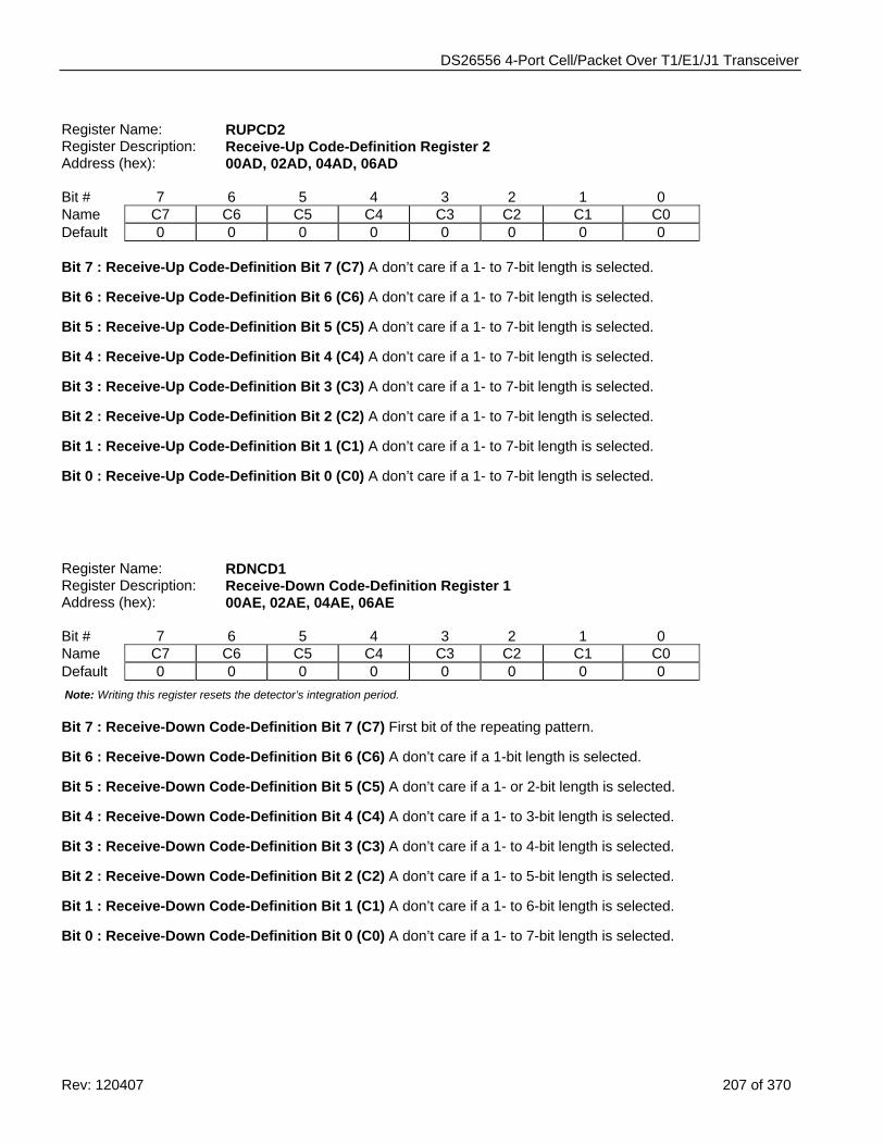
DS26556 4-Port Cell/Packet Over T1/E1/J1 Transceiver
Rev: 120407 207 of 370
Register Name: RUPCD2 Register Description: Receive-Up Code-Definition Register 2 Address (hex): 00AD, 02AD, 04AD, 06AD Bit # 7 6 5 4 3 2 1 0 Name C7 C6 C5 C4 C3 C2 C1 C0 Default 0 0 0 0 0 0 0 0 Bit 7 : Receive-Up Code-Definition Bit 7 (C7) A don’t care if a 1- to 7-bit length is selected.
Bit 6 : Receive-Up Code-Definition Bit 6 (C6) A don’t care if a 1- to 7-bit length is selected.
Bit 5 : Receive-Up Code-Definition Bit 5 (C5) A don’t care if a 1- to 7-bit length is selected.
Bit 4 : Receive-Up Code-Definition Bit 4 (C4) A don’t care if a 1- to 7-bit length is selected.
Bit 3 : Receive-Up Code-Definition Bit 3 (C3) A don’t care if a 1- to 7-bit length is selected.
Bit 2 : Receive-Up Code-Definition Bit 2 (C2) A don’t care if a 1- to 7-bit length is selected.
Bit 1 : Receive-Up Code-Definition Bit 1 (C1) A don’t care if a 1- to 7-bit length is selected.
Bit 0 : Receive-Up Code-Definition Bit 0 (C0) A don’t care if a 1- to 7-bit length is selected.
Register Name: RDNCD1 Register Description: Receive-Down Code-Definition Register 1 Address (hex): 00AE, 02AE, 04AE, 06AE Bit # 7 6 5 4 3 2 1 0 Name C7 C6 C5 C4 C3 C2 C1 C0 Default 0 0 0 0 0 0 0 0 Note: Writing this register resets the detector’s integration period. Bit 7 : Receive-Down Code-Definition Bit 7 (C7) First bit of the repeating pattern.
Bit 6 : Receive-Down Code-Definition Bit 6 (C6) A don’t care if a 1-bit length is selected.
Bit 5 : Receive-Down Code-Definition Bit 5 (C5) A don’t care if a 1- or 2-bit length is selected.
Bit 4 : Receive-Down Code-Definition Bit 4 (C4) A don’t care if a 1- to 3-bit length is selected.
Bit 3 : Receive-Down Code-Definition Bit 3 (C3) A don’t care if a 1- to 4-bit length is selected.
Bit 2 : Receive-Down Code-Definition Bit 2 (C2) A don’t care if a 1- to 5-bit length is selected.
Bit 1 : Receive-Down Code-Definition Bit 1 (C1) A don’t care if a 1- to 6-bit length is selected.
Bit 0 : Receive-Down Code-Definition Bit 0 (C0) A don’t care if a 1- to 7-bit length is selected.

DS26556 4-Port Cell/Packet Over T1/E1/J1 Transceiver
Rev: 120407 208 of 370
Register Name: RDNCD2 Register Description: Receive-Down Code-Definition Register 2 Address (hex): 00AF, 02AF, 04AF, 06AF Bit # 7 6 5 4 3 2 1 0 Name C7 C6 C5 C4 C3 C2 C1 C0 Default 0 0 0 0 0 0 0 0 Bit 7 : Receive-Down Code-Definition Bit 7 (C7) A don’t care if a 1- to 7-bit length is selected.
Bit 6 : Receive-Down Code-Definition Bit 6 (C6) A don’t care if a 1- to 7-bit length is selected.
Bit 5 : Receive-Down Code-Definition Bit 5 (C5) A don’t care if a 1- to 7-bit length is selected.
Bit 4 : Receive-Down Code-Definition Bit 4 (C4) A don’t care if a 1- to 7-bit length is selected.
Bit 3 : Receive-Down Code-Definition Bit 3 (C3) A don’t care if a 1- to 7-bit length is selected.
Bit 2 : Receive-Down Code-Definition Bit 2 (C2) A don’t care if a 1- to 7-bit length is selected.
Bit 1 : Receive-Down Code-Definition Bit 1 (C1) A don’t care if a 1- to 7-bit length is selected.
Bit 0 : Receive-Down Code Definition Bit 0 (C0) A don’t care if a 1- to 7-bit length is selected.
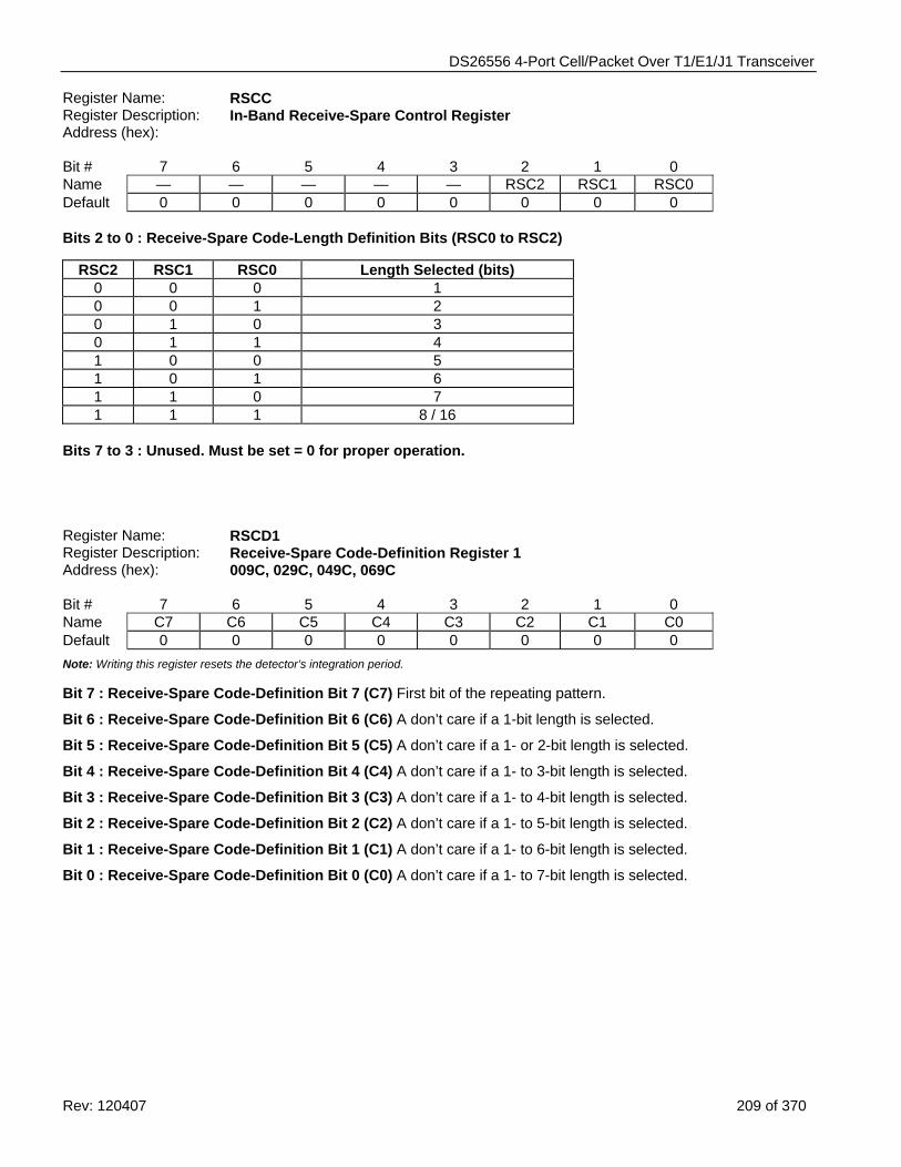
DS26556 4-Port Cell/Packet Over T1/E1/J1 Transceiver
Rev: 120407 209 of 370
Register Name: RSCC Register Description: In-Band Receive-Spare Control Register Address (hex): Bit # 7 6 5 4 3 2 1 0 Name — — — — — RSC2 RSC1 RSC0 Default 0 0 0 0 0 0 0 0 Bits 2 to 0 : Receive-Spare Code-Length Definition Bits (RSC0 to RSC2)
RSC2 RSC1 RSC0 Length Selected (bits) 0 0 0 1 0 0 1 2 0 1 0 3 0 1 1 4 1 0 0 5 1 0 1 6 1 1 0 7 1 1 1 8 / 16
Bits 7 to 3 : Unused. Must be set = 0 for proper operation. Register Name: RSCD1 Register Description: Receive-Spare Code-Definition Register 1 Address (hex): 009C, 029C, 049C, 069C Bit # 7 6 5 4 3 2 1 0 Name C7 C6 C5 C4 C3 C2 C1 C0 Default 0 0 0 0 0 0 0 0 Note: Writing this register resets the detector’s integration period. Bit 7 : Receive-Spare Code-Definition Bit 7 (C7) First bit of the repeating pattern.
Bit 6 : Receive-Spare Code-Definition Bit 6 (C6) A don’t care if a 1-bit length is selected.
Bit 5 : Receive-Spare Code-Definition Bit 5 (C5) A don’t care if a 1- or 2-bit length is selected.
Bit 4 : Receive-Spare Code-Definition Bit 4 (C4) A don’t care if a 1- to 3-bit length is selected.
Bit 3 : Receive-Spare Code-Definition Bit 3 (C3) A don’t care if a 1- to 4-bit length is selected.
Bit 2 : Receive-Spare Code-Definition Bit 2 (C2) A don’t care if a 1- to 5-bit length is selected.
Bit 1 : Receive-Spare Code-Definition Bit 1 (C1) A don’t care if a 1- to 6-bit length is selected.
Bit 0 : Receive-Spare Code-Definition Bit 0 (C0) A don’t care if a 1- to 7-bit length is selected.
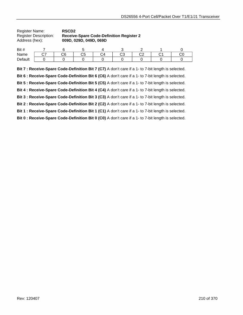
DS26556 4-Port Cell/Packet Over T1/E1/J1 Transceiver
Rev: 120407 210 of 370
Register Name: RSCD2 Register Description: Receive-Spare Code-Definition Register 2 Address (hex): 009D, 029D, 049D, 069D Bit # 7 6 5 4 3 2 1 0 Name C7 C6 C5 C4 C3 C2 C1 C0 Default 0 0 0 0 0 0 0 0 Bit 7 : Receive-Spare Code-Definition Bit 7 (C7) A don’t care if a 1- to 7-bit length is selected.
Bit 6 : Receive-Spare Code-Definition Bit 6 (C6) A don’t care if a 1- to 7-bit length is selected.
Bit 5 : Receive-Spare Code-Definition Bit 5 (C5) A don’t care if a 1- to 7-bit length is selected.
Bit 4 : Receive-Spare Code-Definition Bit 4 (C4) A don’t care if a 1- to 7-bit length is selected.
Bit 3 : Receive-Spare Code-Definition Bit 3 (C3) A don’t care if a 1- to 7-bit length is selected.
Bit 2 : Receive-Spare Code-Definition Bit 2 (C2) A don’t care if a 1- to 7-bit length is selected.
Bit 1 : Receive-Spare Code-Definition Bit 1 (C1) A don’t care if a 1- to 7-bit length is selected.
Bit 0 : Receive-Spare Code-Definition Bit 0 (C0) A don’t care if a 1- to 7-bit length is selected.
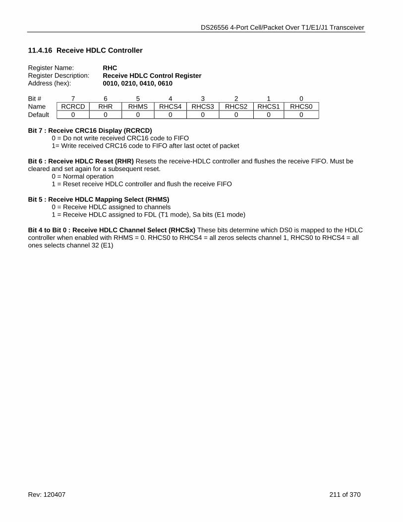
DS26556 4-Port Cell/Packet Over T1/E1/J1 Transceiver
Rev: 120407 211 of 370
11.4.16 Receive HDLC Controller Register Name: RHC Register Description: Receive HDLC Control Register Address (hex): 0010, 0210, 0410, 0610 Bit # 7 6 5 4 3 2 1 0 Name RCRCD RHR RHMS RHCS4 RHCS3 RHCS2 RHCS1 RHCS0 Default 0 0 0 0 0 0 0 0 Bit 7 : Receive CRC16 Display (RCRCD) 0 = Do not write received CRC16 code to FIFO 1= Write received CRC16 code to FIFO after last octet of packet Bit 6 : Receive HDLC Reset (RHR) Resets the receive-HDLC controller and flushes the receive FIFO. Must be cleared and set again for a subsequent reset.
0 = Normal operation 1 = Reset receive HDLC controller and flush the receive FIFO Bit 5 : Receive HDLC Mapping Select (RHMS)
0 = Receive HDLC assigned to channels 1 = Receive HDLC assigned to FDL (T1 mode), Sa bits (E1 mode)
Bit 4 to Bit 0 : Receive HDLC Channel Select (RHCSx) These bits determine which DS0 is mapped to the HDLC controller when enabled with RHMS = 0. RHCS0 to RHCS4 = all zeros selects channel 1, RHCS0 to RHCS4 = all ones selects channel 32 (E1)
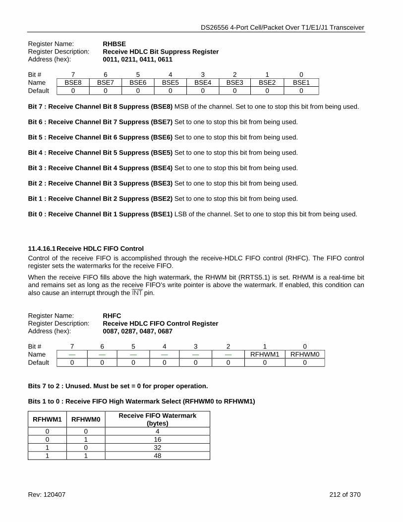
DS26556 4-Port Cell/Packet Over T1/E1/J1 Transceiver
Rev: 120407 212 of 370
Register Name: RHBSE Register Description: Receive HDLC Bit Suppress Register Address (hex): 0011, 0211, 0411, 0611 Bit # 7 6 5 4 3 2 1 0 Name BSE8 BSE7 BSE6 BSE5 BSE4 BSE3 BSE2 BSE1 Default 0 0 0 0 0 0 0 0 Bit 7 : Receive Channel Bit 8 Suppress (BSE8) MSB of the channel. Set to one to stop this bit from being used. Bit 6 : Receive Channel Bit 7 Suppress (BSE7) Set to one to stop this bit from being used. Bit 5 : Receive Channel Bit 6 Suppress (BSE6) Set to one to stop this bit from being used. Bit 4 : Receive Channel Bit 5 Suppress (BSE5) Set to one to stop this bit from being used. Bit 3 : Receive Channel Bit 4 Suppress (BSE4) Set to one to stop this bit from being used. Bit 2 : Receive Channel Bit 3 Suppress (BSE3) Set to one to stop this bit from being used. Bit 1 : Receive Channel Bit 2 Suppress (BSE2) Set to one to stop this bit from being used. Bit 0 : Receive Channel Bit 1 Suppress (BSE1) LSB of the channel. Set to one to stop this bit from being used.
11.4.16.1 Receive HDLC FIFO Control Control of the receive FIFO is accomplished through the receive-HDLC FIFO control (RHFC). The FIFO control register sets the watermarks for the receive FIFO.
When the receive FIFO fills above the high watermark, the RHWM bit (RRTS5.1) is set. RHWM is a real-time bit and remains set as long as the receive FIFO’s write pointer is above the watermark. If enabled, this condition can also cause an interrupt through the INT pin. Register Name: RHFC Register Description: Receive HDLC FIFO Control Register Address (hex): 0087, 0287, 0487, 0687 Bit # 7 6 5 4 3 2 1 0 Name — — — — — — RFHWM1 RFHWM0 Default 0 0 0 0 0 0 0 0 Bits 7 to 2 : Unused. Must be set = 0 for proper operation. Bits 1 to 0 : Receive FIFO High Watermark Select (RFHWM0 to RFHWM1)
RFHWM1 RFHWM0 Receive FIFO Watermark (bytes)
0 0 4 0 1 16 1 0 32 1 1 48
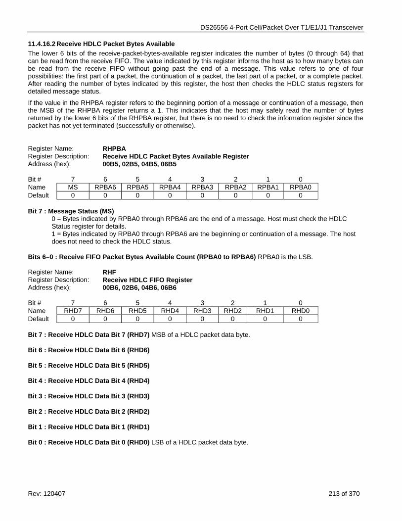
DS26556 4-Port Cell/Packet Over T1/E1/J1 Transceiver
Rev: 120407 213 of 370
11.4.16.2 Receive HDLC Packet Bytes Available The lower 6 bits of the receive-packet-bytes-available register indicates the number of bytes (0 through 64) that can be read from the receive FIFO. The value indicated by this register informs the host as to how many bytes can be read from the receive FIFO without going past the end of a message. This value refers to one of four possibilities: the first part of a packet, the continuation of a packet, the last part of a packet, or a complete packet. After reading the number of bytes indicated by this register, the host then checks the HDLC status registers for detailed message status.
If the value in the RHPBA register refers to the beginning portion of a message or continuation of a message, then the MSB of the RHPBA register returns a 1. This indicates that the host may safely read the number of bytes returned by the lower 6 bits of the RHPBA register, but there is no need to check the information register since the packet has not yet terminated (successfully or otherwise). Register Name: RHPBA Register Description: Receive HDLC Packet Bytes Available Register Address (hex): 00B5, 02B5, 04B5, 06B5 Bit # 7 6 5 4 3 2 1 0 Name MS RPBA6 RPBA5 RPBA4 RPBA3 RPBA2 RPBA1 RPBA0 Default 0 0 0 0 0 0 0 0 Bit 7 : Message Status (MS)
0 = Bytes indicated by RPBA0 through RPBA6 are the end of a message. Host must check the HDLC Status register for details. 1 = Bytes indicated by RPBA0 through RPBA6 are the beginning or continuation of a message. The host does not need to check the HDLC status.
Bits 6–0 : Receive FIFO Packet Bytes Available Count (RPBA0 to RPBA6) RPBA0 is the LSB. Register Name: RHF Register Description: Receive HDLC FIFO Register Address (hex): 00B6, 02B6, 04B6, 06B6 Bit # 7 6 5 4 3 2 1 0 Name RHD7 RHD6 RHD5 RHD4 RHD3 RHD2 RHD1 RHD0 Default 0 0 0 0 0 0 0 0 Bit 7 : Receive HDLC Data Bit 7 (RHD7) MSB of a HDLC packet data byte. Bit 6 : Receive HDLC Data Bit 6 (RHD6) Bit 5 : Receive HDLC Data Bit 5 (RHD5) Bit 4 : Receive HDLC Data Bit 4 (RHD4) Bit 3 : Receive HDLC Data Bit 3 (RHD3) Bit 2 : Receive HDLC Data Bit 2 (RHD2) Bit 1 : Receive HDLC Data Bit 1 (RHD1) Bit 0 : Receive HDLC Data Bit 0 (RHD0) LSB of a HDLC packet data byte.
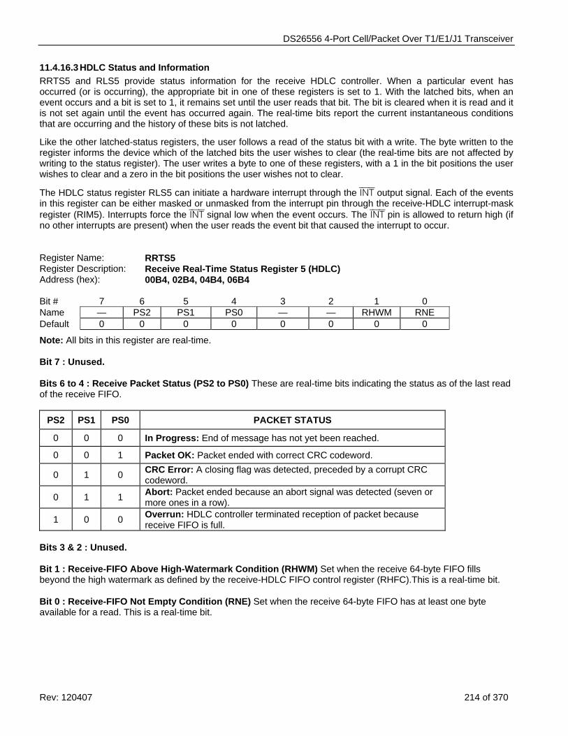
DS26556 4-Port Cell/Packet Over T1/E1/J1 Transceiver
Rev: 120407 214 of 370
11.4.16.3 HDLC Status and Information RRTS5 and RLS5 provide status information for the receive HDLC controller. When a particular event has occurred (or is occurring), the appropriate bit in one of these registers is set to 1. With the latched bits, when an event occurs and a bit is set to 1, it remains set until the user reads that bit. The bit is cleared when it is read and it is not set again until the event has occurred again. The real-time bits report the current instantaneous conditions that are occurring and the history of these bits is not latched.
Like the other latched-status registers, the user follows a read of the status bit with a write. The byte written to the register informs the device which of the latched bits the user wishes to clear (the real-time bits are not affected by writing to the status register). The user writes a byte to one of these registers, with a 1 in the bit positions the user wishes to clear and a zero in the bit positions the user wishes not to clear.
The HDLC status register RLS5 can initiate a hardware interrupt through the INT output signal. Each of the events in this register can be either masked or unmasked from the interrupt pin through the receive-HDLC interrupt-mask register (RIM5). Interrupts force the INT signal low when the event occurs. The INT pin is allowed to return high (if no other interrupts are present) when the user reads the event bit that caused the interrupt to occur. Register Name: RRTS5 Register Description: Receive Real-Time Status Register 5 (HDLC) Address (hex): 00B4, 02B4, 04B4, 06B4 Bit # 7 6 5 4 3 2 1 0 Name — PS2 PS1 PS0 — — RHWM RNE Default 0 0 0 0 0 0 0 0
Note: All bits in this register are real-time. Bit 7 : Unused. Bits 6 to 4 : Receive Packet Status (PS2 to PS0) These are real-time bits indicating the status as of the last read of the receive FIFO.
PS2 PS1 PS0 PACKET STATUS
0 0 0 In Progress: End of message has not yet been reached.
0 0 1 Packet OK: Packet ended with correct CRC codeword.
0 1 0 CRC Error: A closing flag was detected, preceded by a corrupt CRC codeword.
0 1 1 Abort: Packet ended because an abort signal was detected (seven or more ones in a row).
1 0 0 Overrun: HDLC controller terminated reception of packet because receive FIFO is full.
Bits 3 & 2 : Unused. Bit 1 : Receive-FIFO Above High-Watermark Condition (RHWM) Set when the receive 64-byte FIFO fills beyond the high watermark as defined by the receive-HDLC FIFO control register (RHFC).This is a real-time bit. Bit 0 : Receive-FIFO Not Empty Condition (RNE) Set when the receive 64-byte FIFO has at least one byte available for a read. This is a real-time bit.
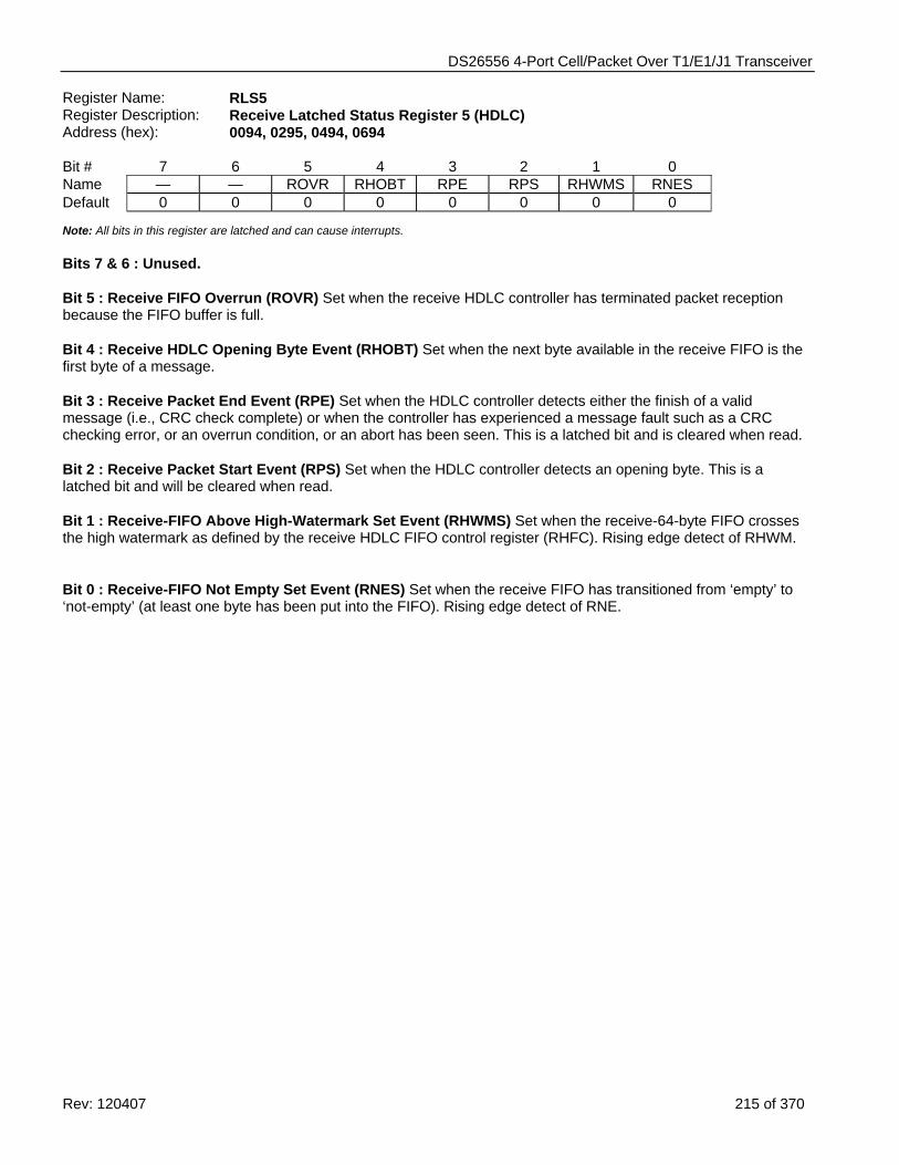
DS26556 4-Port Cell/Packet Over T1/E1/J1 Transceiver
Rev: 120407 215 of 370
Register Name: RLS5 Register Description: Receive Latched Status Register 5 (HDLC) Address (hex): 0094, 0295, 0494, 0694 Bit # 7 6 5 4 3 2 1 0 Name — — ROVR RHOBT RPE RPS RHWMS RNES Default 0 0 0 0 0 0 0 0
Note: All bits in this register are latched and can cause interrupts. Bits 7 & 6 : Unused. Bit 5 : Receive FIFO Overrun (ROVR) Set when the receive HDLC controller has terminated packet reception because the FIFO buffer is full. Bit 4 : Receive HDLC Opening Byte Event (RHOBT) Set when the next byte available in the receive FIFO is the first byte of a message. Bit 3 : Receive Packet End Event (RPE) Set when the HDLC controller detects either the finish of a valid message (i.e., CRC check complete) or when the controller has experienced a message fault such as a CRC checking error, or an overrun condition, or an abort has been seen. This is a latched bit and is cleared when read. Bit 2 : Receive Packet Start Event (RPS) Set when the HDLC controller detects an opening byte. This is a latched bit and will be cleared when read. Bit 1 : Receive-FIFO Above High-Watermark Set Event (RHWMS) Set when the receive-64-byte FIFO crosses the high watermark as defined by the receive HDLC FIFO control register (RHFC). Rising edge detect of RHWM. Bit 0 : Receive-FIFO Not Empty Set Event (RNES) Set when the receive FIFO has transitioned from ‘empty’ to ‘not-empty’ (at least one byte has been put into the FIFO). Rising edge detect of RNE.
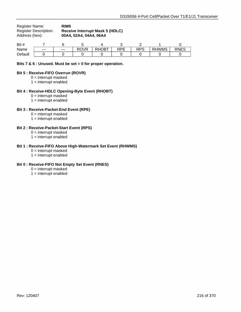
DS26556 4-Port Cell/Packet Over T1/E1/J1 Transceiver
Rev: 120407 216 of 370
Register Name: RIM5 Register Description: Receive Interrupt Mask 5 (HDLC) Address (hex): 00A4, 02A4, 04A4, 06A4 Bit # 7 6 5 4 3 2 1 0 Name — — ROVR RHOBT RPE RPS RHWMS RNES Default 0 0 0 0 0 0 0 0 Bits 7 & 6 : Unused. Must be set = 0 for proper operation. Bit 5 : Receive-FIFO Overrun (ROVR)
0 = interrupt masked 1 = interrupt enabled
Bit 4 : Receive-HDLC Opening-Byte Event (RHOBT)
0 = interrupt masked 1 = interrupt enabled
Bit 3 : Receive-Packet-End Event (RPE)
0 = interrupt masked 1 = interrupt enabled
Bit 2 : Receive-Packet-Start Event (RPS)
0 = interrupt masked 1 = interrupt enabled
Bit 1 : Receive-FIFO Above High-Watermark Set Event (RHWMS)
0 = interrupt masked 1 = interrupt enabled
Bit 0 : Receive-FIFO Not Empty Set Event (RNES)
0 = interrupt masked 1 = interrupt enabled
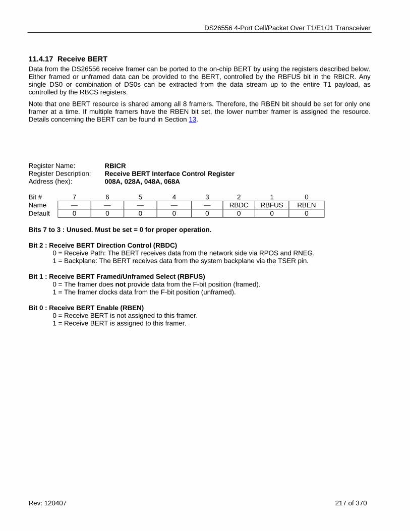
DS26556 4-Port Cell/Packet Over T1/E1/J1 Transceiver
Rev: 120407 217 of 370
11.4.17 Receive BERT Data from the DS26556 receive framer can be ported to the on-chip BERT by using the registers described below. Either framed or unframed data can be provided to the BERT, controlled by the RBFUS bit in the RBICR. Any single DS0 or combination of DS0s can be extracted from the data stream up to the entire T1 payload, as controlled by the RBCS registers.
Note that one BERT resource is shared among all 8 framers. Therefore, the RBEN bit should be set for only one framer at a time. If multiple framers have the RBEN bit set, the lower number framer is assigned the resource. Details concerning the BERT can be found in Section 13. Register Name: RBICR Register Description: Receive BERT Interface Control Register Address (hex): 008A, 028A, 048A, 068A Bit # 7 6 5 4 3 2 1 0 Name — — — — — RBDC RBFUS RBEN Default 0 0 0 0 0 0 0 0 Bits 7 to 3 : Unused. Must be set = 0 for proper operation. Bit 2 : Receive BERT Direction Control (RBDC) 0 = Receive Path: The BERT receives data from the network side via RPOS and RNEG.
1 = Backplane: The BERT receives data from the system backplane via the TSER pin.
Bit 1 : Receive BERT Framed/Unframed Select (RBFUS) 0 = The framer does not provide data from the F-bit position (framed). 1 = The framer clocks data from the F-bit position (unframed).
Bit 0 : Receive BERT Enable (RBEN) 0 = Receive BERT is not assigned to this framer.
1 = Receive BERT is assigned to this framer.
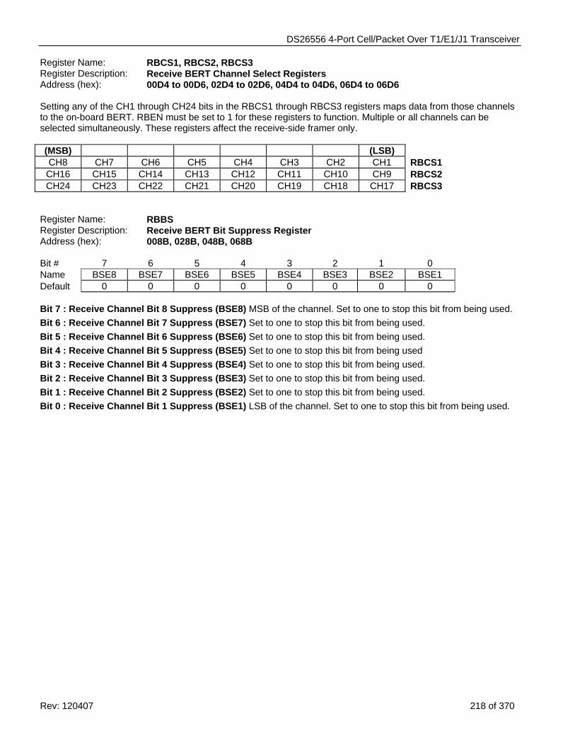
DS26556 4-Port Cell/Packet Over T1/E1/J1 Transceiver
Rev: 120407 218 of 370
Register Name: RBCS1, RBCS2, RBCS3 Register Description: Receive BERT Channel Select Registers Address (hex): 00D4 to 00D6, 02D4 to 02D6, 04D4 to 04D6, 06D4 to 06D6 Setting any of the CH1 through CH24 bits in the RBCS1 through RBCS3 registers maps data from those channels to the on-board BERT. RBEN must be set to 1 for these registers to function. Multiple or all channels can be selected simultaneously. These registers affect the receive-side framer only. (MSB) (LSB) CH8 CH7 CH6 CH5 CH4 CH3 CH2 CH1 RBCS1 CH16 CH15 CH14 CH13 CH12 CH11 CH10 CH9 RBCS2 CH24 CH23 CH22 CH21 CH20 CH19 CH18 CH17 RBCS3
Register Name: RBBS Register Description: Receive BERT Bit Suppress Register Address (hex): 008B, 028B, 048B, 068B Bit # 7 6 5 4 3 2 1 0 Name BSE8 BSE7 BSE6 BSE5 BSE4 BSE3 BSE2 BSE1 Default 0 0 0 0 0 0 0 0 Bit 7 : Receive Channel Bit 8 Suppress (BSE8) MSB of the channel. Set to one to stop this bit from being used. Bit 6 : Receive Channel Bit 7 Suppress (BSE7) Set to one to stop this bit from being used. Bit 5 : Receive Channel Bit 6 Suppress (BSE6) Set to one to stop this bit from being used. Bit 4 : Receive Channel Bit 5 Suppress (BSE5) Set to one to stop this bit from being used Bit 3 : Receive Channel Bit 4 Suppress (BSE4) Set to one to stop this bit from being used. Bit 2 : Receive Channel Bit 3 Suppress (BSE3) Set to one to stop this bit from being used. Bit 1 : Receive Channel Bit 2 Suppress (BSE2) Set to one to stop this bit from being used. Bit 0 : Receive Channel Bit 1 Suppress (BSE1) LSB of the channel. Set to one to stop this bit from being used.
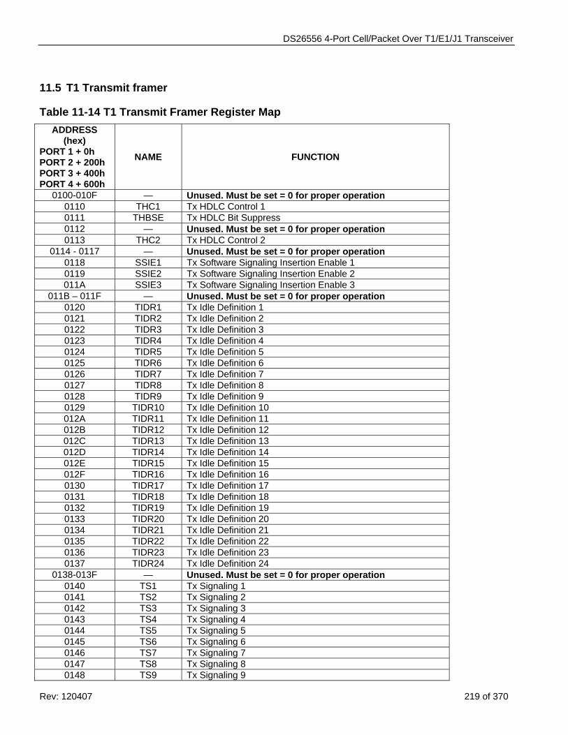
DS26556 4-Port Cell/Packet Over T1/E1/J1 Transceiver
Rev: 120407 219 of 370
11.5 T1 Transmit framer
Table 11-14 T1 Transmit Framer Register Map ADDRESS
(hex) PORT 1 + 0h PORT 2 + 200h PORT 3 + 400h PORT 4 + 600h
NAME FUNCTION
0100-010F — Unused. Must be set = 0 for proper operation 0110 THC1 Tx HDLC Control 1 0111 THBSE Tx HDLC Bit Suppress 0112 — Unused. Must be set = 0 for proper operation 0113 THC2 Tx HDLC Control 2
0114 - 0117 — Unused. Must be set = 0 for proper operation 0118 SSIE1 Tx Software Signaling Insertion Enable 1 0119 SSIE2 Tx Software Signaling Insertion Enable 2 011A SSIE3 Tx Software Signaling Insertion Enable 3
011B – 011F — Unused. Must be set = 0 for proper operation 0120 TIDR1 Tx Idle Definition 1 0121 TIDR2 Tx Idle Definition 2 0122 TIDR3 Tx Idle Definition 3 0123 TIDR4 Tx Idle Definition 4 0124 TIDR5 Tx Idle Definition 5 0125 TIDR6 Tx Idle Definition 6 0126 TIDR7 Tx Idle Definition 7 0127 TIDR8 Tx Idle Definition 8 0128 TIDR9 Tx Idle Definition 9 0129 TIDR10 Tx Idle Definition 10 012A TIDR11 Tx Idle Definition 11 012B TIDR12 Tx Idle Definition 12 012C TIDR13 Tx Idle Definition 13 012D TIDR14 Tx Idle Definition 14 012E TIDR15 Tx Idle Definition 15 012F TIDR16 Tx Idle Definition 16 0130 TIDR17 Tx Idle Definition 17 0131 TIDR18 Tx Idle Definition 18 0132 TIDR19 Tx Idle Definition 19 0133 TIDR20 Tx Idle Definition 20 0134 TIDR21 Tx Idle Definition 21 0135 TIDR22 Tx Idle Definition 22 0136 TIDR23 Tx Idle Definition 23 0137 TIDR24 Tx Idle Definition 24
0138-013F — Unused. Must be set = 0 for proper operation 0140 TS1 Tx Signaling 1 0141 TS2 Tx Signaling 2 0142 TS3 Tx Signaling 3 0143 TS4 Tx Signaling 4 0144 TS5 Tx Signaling 5 0145 TS6 Tx Signaling 6 0146 TS7 Tx Signaling 7 0147 TS8 Tx Signaling 8 0148 TS9 Tx Signaling 9
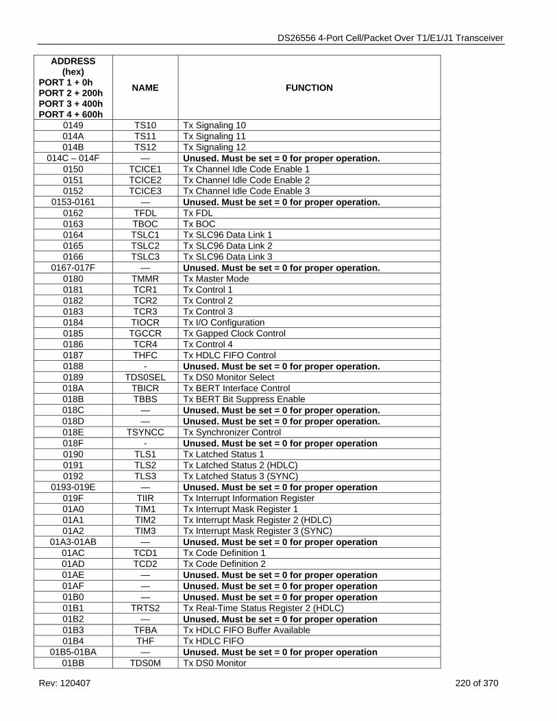
DS26556 4-Port Cell/Packet Over T1/E1/J1 Transceiver
Rev: 120407 220 of 370
ADDRESS (hex)
PORT 1 + 0h PORT 2 + 200h PORT 3 + 400h PORT 4 + 600h
NAME FUNCTION
0149 TS10 Tx Signaling 10 014A TS11 Tx Signaling 11 014B TS12 Tx Signaling 12
014C – 014F — Unused. Must be set = 0 for proper operation. 0150 TCICE1 Tx Channel Idle Code Enable 1 0151 TCICE2 Tx Channel Idle Code Enable 2 0152 TCICE3 Tx Channel Idle Code Enable 3
0153-0161 — Unused. Must be set = 0 for proper operation. 0162 TFDL Tx FDL 0163 TBOC Tx BOC 0164 TSLC1 Tx SLC96 Data Link 1 0165 TSLC2 Tx SLC96 Data Link 2 0166 TSLC3 Tx SLC96 Data Link 3
0167-017F — Unused. Must be set = 0 for proper operation. 0180 TMMR Tx Master Mode 0181 TCR1 Tx Control 1 0182 TCR2 Tx Control 2 0183 TCR3 Tx Control 3 0184 TIOCR Tx I/O Configuration 0185 TGCCR Tx Gapped Clock Control 0186 TCR4 Tx Control 4 0187 THFC Tx HDLC FIFO Control 0188 - Unused. Must be set = 0 for proper operation. 0189 TDS0SEL Tx DS0 Monitor Select 018A TBICR Tx BERT Interface Control 018B TBBS Tx BERT Bit Suppress Enable 018C — Unused. Must be set = 0 for proper operation. 018D — Unused. Must be set = 0 for proper operation. 018E TSYNCC Tx Synchronizer Control 018F - Unused. Must be set = 0 for proper operation 0190 TLS1 Tx Latched Status 1 0191 TLS2 Tx Latched Status 2 (HDLC) 0192 TLS3 Tx Latched Status 3 (SYNC)
0193-019E — Unused. Must be set = 0 for proper operation 019F TIIR Tx Interrupt Information Register 01A0 TIM1 Tx Interrupt Mask Register 1 01A1 TIM2 Tx Interrupt Mask Register 2 (HDLC) 01A2 TIM3 Tx Interrupt Mask Register 3 (SYNC)
01A3-01AB — Unused. Must be set = 0 for proper operation 01AC TCD1 Tx Code Definition 1 01AD TCD2 Tx Code Definition 2 01AE — Unused. Must be set = 0 for proper operation 01AF — Unused. Must be set = 0 for proper operation 01B0 — Unused. Must be set = 0 for proper operation 01B1 TRTS2 Tx Real-Time Status Register 2 (HDLC) 01B2 — Unused. Must be set = 0 for proper operation 01B3 TFBA Tx HDLC FIFO Buffer Available 01B4 THF Tx HDLC FIFO
01B5-01BA — Unused. Must be set = 0 for proper operation 01BB TDS0M Tx DS0 Monitor
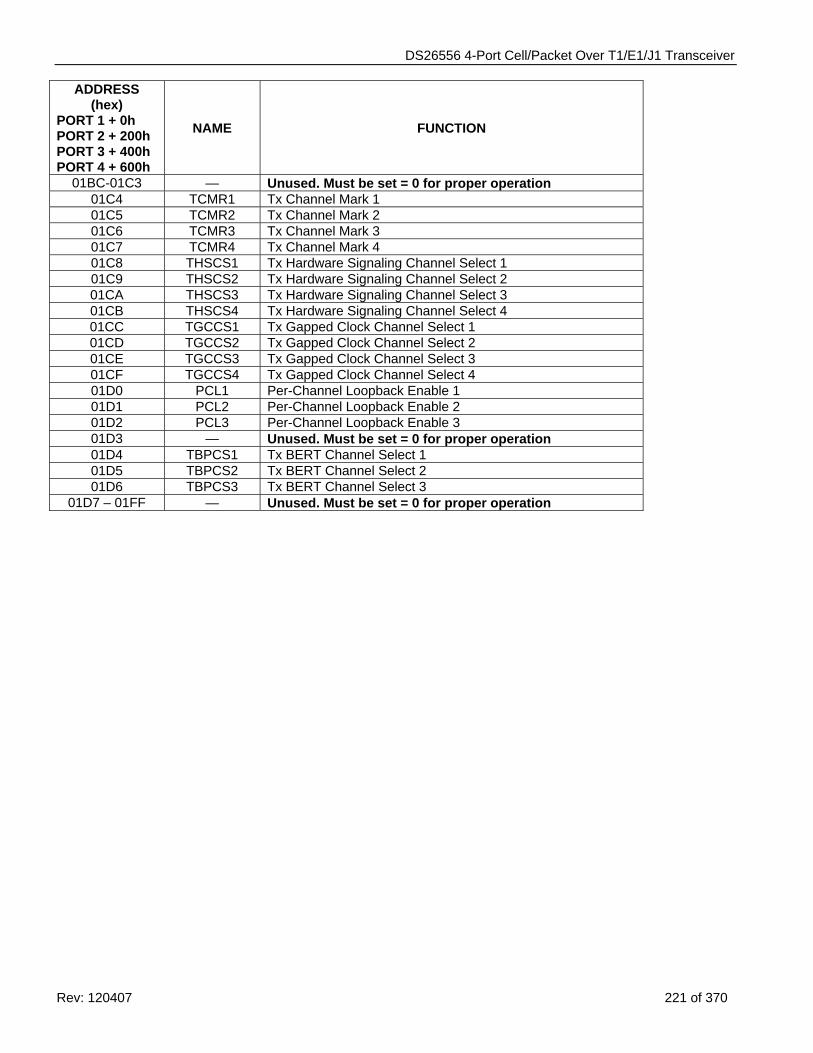
DS26556 4-Port Cell/Packet Over T1/E1/J1 Transceiver
Rev: 120407 221 of 370
ADDRESS (hex)
PORT 1 + 0h PORT 2 + 200h PORT 3 + 400h PORT 4 + 600h
NAME FUNCTION
01BC-01C3 — Unused. Must be set = 0 for proper operation 01C4 TCMR1 Tx Channel Mark 1 01C5 TCMR2 Tx Channel Mark 2 01C6 TCMR3 Tx Channel Mark 3 01C7 TCMR4 Tx Channel Mark 4 01C8 THSCS1 Tx Hardware Signaling Channel Select 1 01C9 THSCS2 Tx Hardware Signaling Channel Select 2 01CA THSCS3 Tx Hardware Signaling Channel Select 3 01CB THSCS4 Tx Hardware Signaling Channel Select 4 01CC TGCCS1 Tx Gapped Clock Channel Select 1 01CD TGCCS2 Tx Gapped Clock Channel Select 2 01CE TGCCS3 Tx Gapped Clock Channel Select 3 01CF TGCCS4 Tx Gapped Clock Channel Select 4 01D0 PCL1 Per-Channel Loopback Enable 1 01D1 PCL2 Per-Channel Loopback Enable 2 01D2 PCL3 Per-Channel Loopback Enable 3 01D3 — Unused. Must be set = 0 for proper operation 01D4 TBPCS1 Tx BERT Channel Select 1 01D5 TBPCS2 Tx BERT Channel Select 2 01D6 TBPCS3 Tx BERT Channel Select 3
01D7 – 01FF — Unused. Must be set = 0 for proper operation
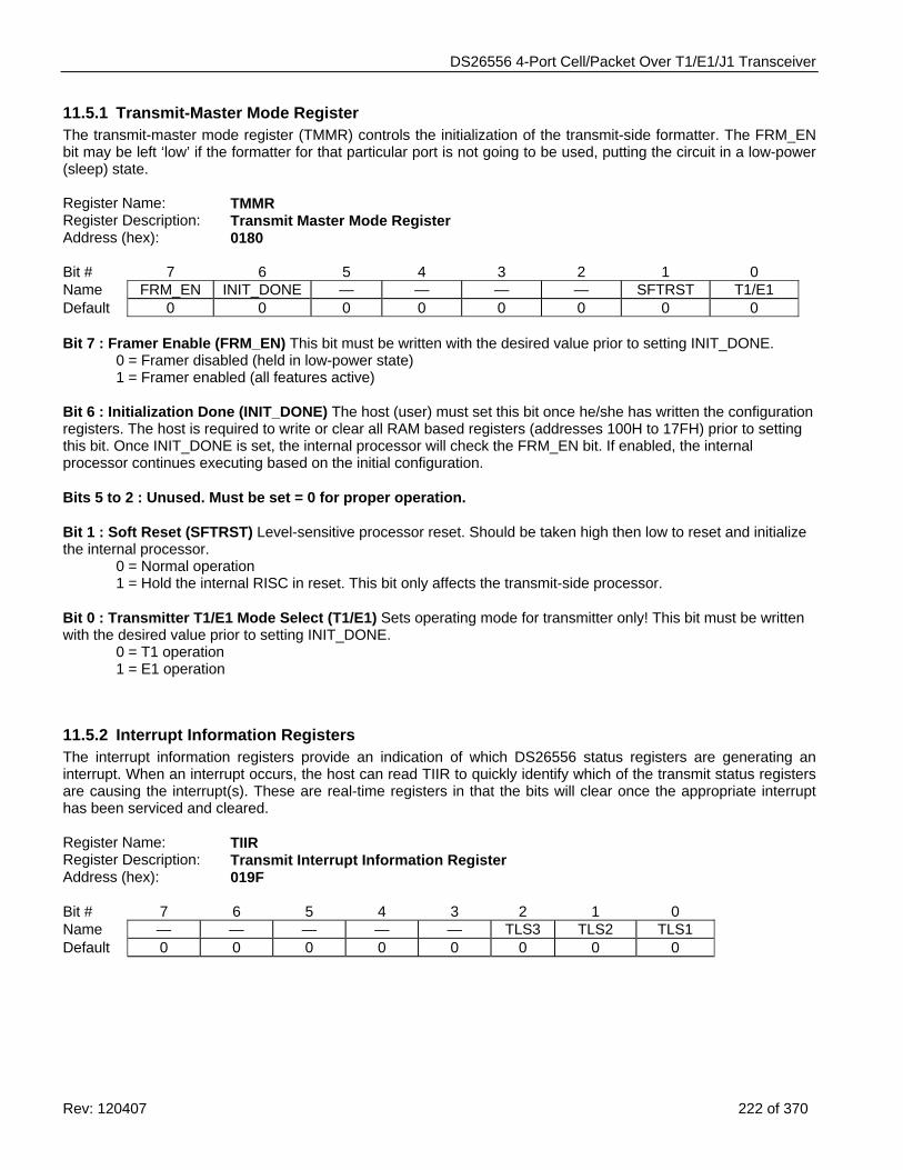
DS26556 4-Port Cell/Packet Over T1/E1/J1 Transceiver
Rev: 120407 222 of 370
11.5.1 Transmit-Master Mode Register The transmit-master mode register (TMMR) controls the initialization of the transmit-side formatter. The FRM_EN bit may be left ‘low’ if the formatter for that particular port is not going to be used, putting the circuit in a low-power (sleep) state. Register Name: TMMR Register Description: Transmit Master Mode Register Address (hex): 0180 Bit # 7 6 5 4 3 2 1 0 Name FRM_EN INIT_DONE — — — — SFTRST T1/E1 Default 0 0 0 0 0 0 0 0 Bit 7 : Framer Enable (FRM_EN) This bit must be written with the desired value prior to setting INIT_DONE. 0 = Framer disabled (held in low-power state) 1 = Framer enabled (all features active) Bit 6 : Initialization Done (INIT_DONE) The host (user) must set this bit once he/she has written the configuration registers. The host is required to write or clear all RAM based registers (addresses 100H to 17FH) prior to setting this bit. Once INIT_DONE is set, the internal processor will check the FRM_EN bit. If enabled, the internal processor continues executing based on the initial configuration. Bits 5 to 2 : Unused. Must be set = 0 for proper operation. Bit 1 : Soft Reset (SFTRST) Level-sensitive processor reset. Should be taken high then low to reset and initialize the internal processor.
0 = Normal operation 1 = Hold the internal RISC in reset. This bit only affects the transmit-side processor.
Bit 0 : Transmitter T1/E1 Mode Select (T1/E1) Sets operating mode for transmitter only! This bit must be written with the desired value prior to setting INIT_DONE.
0 = T1 operation 1 = E1 operation
11.5.2 Interrupt Information Registers The interrupt information registers provide an indication of which DS26556 status registers are generating an interrupt. When an interrupt occurs, the host can read TIIR to quickly identify which of the transmit status registers are causing the interrupt(s). These are real-time registers in that the bits will clear once the appropriate interrupt has been serviced and cleared.
Register Name: TIIR Register Description: Transmit Interrupt Information Register Address (hex): 019F Bit # 7 6 5 4 3 2 1 0 Name — — — — — TLS3 TLS2 TLS1 Default 0 0 0 0 0 0 0 0
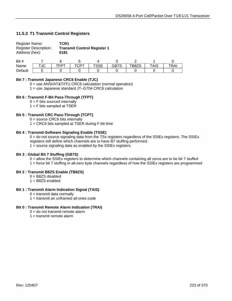
DS26556 4-Port Cell/Packet Over T1/E1/J1 Transceiver
Rev: 120407 223 of 370
11.5.3 T1 Transmit Control Registers
Register Name: TCR1 Register Description: Transmit Control Register 1 Address (hex): 0181 Bit # 7 6 5 4 3 2 1 0 Name TJC TFPT TCPT TSSE GB7S TB8ZS TAIS TRAI Default 0 0 0 0 0 0 0 0 Bit 7 : Transmit Japanese CRC6 Enable (TJC)
0 = use ANSI/AT&T/ITU CRC6 calculation (normal operation) 1 = use Japanese standard JT–G704 CRC6 calculation
Bit 6 : Transmit F-Bit Pass-Through (TFPT)
0 = F bits sourced internally 1 = F bits sampled at TSER
Bit 5 : Transmit CRC Pass-Through (TCPT)
0 = source CRC6 bits internally 1 = CRC6 bits sampled at TSER during F-bit time
Bit 4 : Transmit-Software Signaling Enable (TSSE)
0 = do not source signaling data from the TSx registers regardless of the SSIEx registers. The SSIEx registers still define which channels are to have B7 stuffing performed. 1 = source signaling data as enabled by the SSIEx registers.
Bit 3 : Global Bit 7 Stuffing (GB7S)
0 = allow the SSIEx registers to determine which channels containing all zeros are to be bit 7 stuffed 1 = force bit 7 stuffing in all-zero byte channels regardless of how the SSIEx registers are programmed
Bit 2 : Transmit B8ZS Enable (TB8ZS)
0 = B8ZS disabled 1 = B8ZS enabled
Bit 1 : Transmit Alarm Indication Signal (TAIS)
0 = transmit data normally 1 = transmit an unframed all-ones code
Bit 0 : Transmit Remote Alarm Indication (TRAI)
0 = do not transmit remote alarm 1 = transmit remote alarm
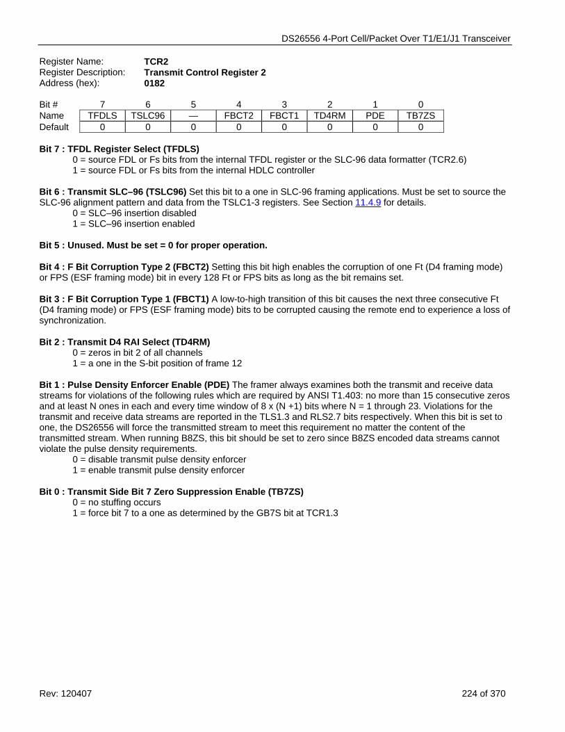
DS26556 4-Port Cell/Packet Over T1/E1/J1 Transceiver
Rev: 120407 224 of 370
Register Name: TCR2 Register Description: Transmit Control Register 2 Address (hex): 0182 Bit # 7 6 5 4 3 2 1 0 Name TFDLS TSLC96 — FBCT2 FBCT1 TD4RM PDE TB7ZS Default 0 0 0 0 0 0 0 0 Bit 7 : TFDL Register Select (TFDLS)
0 = source FDL or Fs bits from the internal TFDL register or the SLC-96 data formatter (TCR2.6) 1 = source FDL or Fs bits from the internal HDLC controller
Bit 6 : Transmit SLC–96 (TSLC96) Set this bit to a one in SLC-96 framing applications. Must be set to source the SLC-96 alignment pattern and data from the TSLC1-3 registers. See Section 11.4.9 for details.
0 = SLC–96 insertion disabled 1 = SLC–96 insertion enabled
Bit 5 : Unused. Must be set = 0 for proper operation. Bit 4 : F Bit Corruption Type 2 (FBCT2) Setting this bit high enables the corruption of one Ft (D4 framing mode) or FPS (ESF framing mode) bit in every 128 Ft or FPS bits as long as the bit remains set. Bit 3 : F Bit Corruption Type 1 (FBCT1) A low-to-high transition of this bit causes the next three consecutive Ft (D4 framing mode) or FPS (ESF framing mode) bits to be corrupted causing the remote end to experience a loss of synchronization. Bit 2 : Transmit D4 RAI Select (TD4RM)
0 = zeros in bit 2 of all channels 1 = a one in the S-bit position of frame 12
Bit 1 : Pulse Density Enforcer Enable (PDE) The framer always examines both the transmit and receive data streams for violations of the following rules which are required by ANSI T1.403: no more than 15 consecutive zeros and at least N ones in each and every time window of 8 x (N +1) bits where N = 1 through 23. Violations for the transmit and receive data streams are reported in the TLS1.3 and RLS2.7 bits respectively. When this bit is set to one, the DS26556 will force the transmitted stream to meet this requirement no matter the content of the transmitted stream. When running B8ZS, this bit should be set to zero since B8ZS encoded data streams cannot violate the pulse density requirements.
0 = disable transmit pulse density enforcer 1 = enable transmit pulse density enforcer
Bit 0 : Transmit Side Bit 7 Zero Suppression Enable (TB7ZS) 0 = no stuffing occurs 1 = force bit 7 to a one as determined by the GB7S bit at TCR1.3
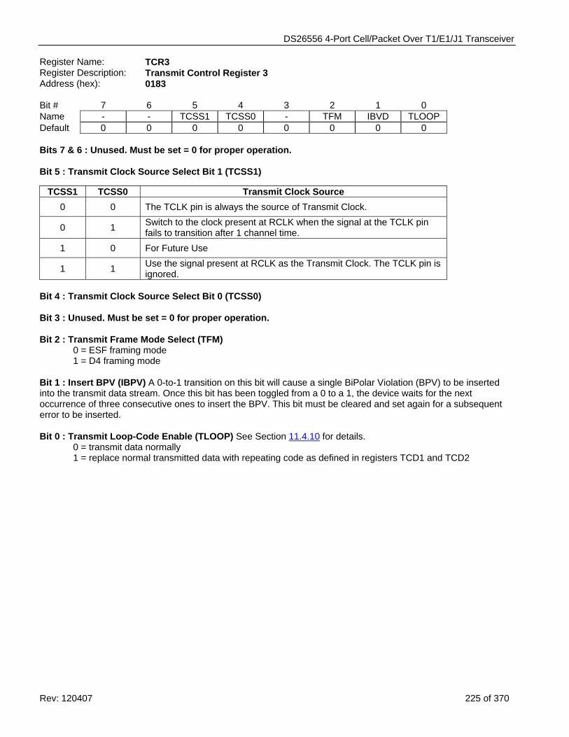
DS26556 4-Port Cell/Packet Over T1/E1/J1 Transceiver
Rev: 120407 225 of 370
Register Name: TCR3 Register Description: Transmit Control Register 3 Address (hex): 0183 Bit # 7 6 5 4 3 2 1 0 Name - - TCSS1 TCSS0 - TFM IBVD TLOOP Default 0 0 0 0 0 0 0 0 Bits 7 & 6 : Unused. Must be set = 0 for proper operation. Bit 5 : Transmit Clock Source Select Bit 1 (TCSS1)
TCSS1 TCSS0 Transmit Clock Source 0 0 The TCLK pin is always the source of Transmit Clock.
0 1 Switch to the clock present at RCLK when the signal at the TCLK pin fails to transition after 1 channel time.
1 0 For Future Use
1 1 Use the signal present at RCLK as the Transmit Clock. The TCLK pin is ignored.
Bit 4 : Transmit Clock Source Select Bit 0 (TCSS0) Bit 3 : Unused. Must be set = 0 for proper operation. Bit 2 : Transmit Frame Mode Select (TFM)
0 = ESF framing mode 1 = D4 framing mode
Bit 1 : Insert BPV (IBPV) A 0-to-1 transition on this bit will cause a single BiPolar Violation (BPV) to be inserted into the transmit data stream. Once this bit has been toggled from a 0 to a 1, the device waits for the next occurrence of three consecutive ones to insert the BPV. This bit must be cleared and set again for a subsequent error to be inserted. Bit 0 : Transmit Loop-Code Enable (TLOOP) See Section 11.4.10 for details.
0 = transmit data normally 1 = replace normal transmitted data with repeating code as defined in registers TCD1 and TCD2
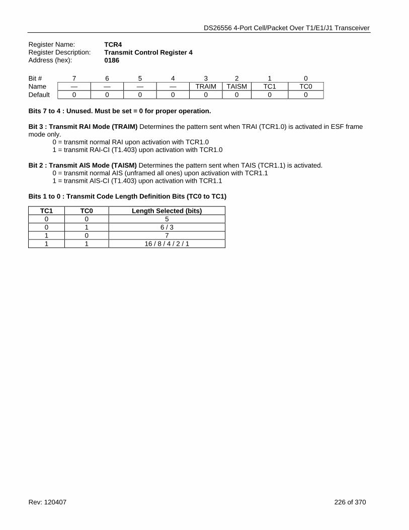
DS26556 4-Port Cell/Packet Over T1/E1/J1 Transceiver
Rev: 120407 226 of 370
Register Name: TCR4 Register Description: Transmit Control Register 4 Address (hex): 0186 Bit # 7 6 5 4 3 2 1 0 Name — — — — TRAIM TAISM TC1 TC0 Default 0 0 0 0 0 0 0 0 Bits 7 to 4 : Unused. Must be set = 0 for proper operation. Bit 3 : Transmit RAI Mode (TRAIM) Determines the pattern sent when TRAI (TCR1.0) is activated in ESF frame mode only. 0 = transmit normal RAI upon activation with TCR1.0 1 = transmit RAI-CI (T1.403) upon activation with TCR1.0 Bit 2 : Transmit AIS Mode (TAISM) Determines the pattern sent when TAIS (TCR1.1) is activated. 0 = transmit normal AIS (unframed all ones) upon activation with TCR1.1 1 = transmit AIS-CI (T1.403) upon activation with TCR1.1 Bits 1 to 0 : Transmit Code Length Definition Bits (TC0 to TC1)
TC1 TC0 Length Selected (bits) 0 0 5 0 1 6 / 3 1 0 7 1 1 16 / 8 / 4 / 2 / 1
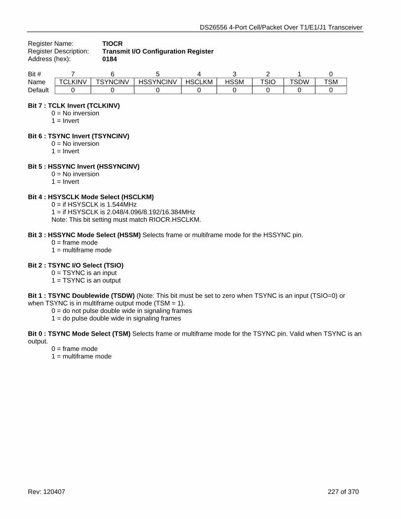
DS26556 4-Port Cell/Packet Over T1/E1/J1 Transceiver
Rev: 120407 227 of 370
Register Name: TIOCR Register Description: Transmit I/O Configuration Register Address (hex): 0184 Bit # 7 6 5 4 3 2 1 0 Name TCLKINV TSYNCINV HSSYNCINV HSCLKM HSSM TSIO TSDW TSM Default 0 0 0 0 0 0 0 0 Bit 7 : TCLK Invert (TCLKINV)
0 = No inversion 1 = Invert
Bit 6 : TSYNC Invert (TSYNCINV)
0 = No inversion 1 = Invert
Bit 5 : HSSYNC Invert (HSSYNCINV)
0 = No inversion 1 = Invert
Bit 4 : HSYSCLK Mode Select (HSCLKM)
0 = if HSYSCLK is 1.544MHz 1 = if HSYSCLK is 2.048/4.096/8.192/16.384MHz Note: This bit setting must match RIOCR.HSCLKM.
Bit 3 : HSSYNC Mode Select (HSSM) Selects frame or multiframe mode for the HSSYNC pin.
0 = frame mode 1 = multiframe mode
Bit 2 : TSYNC I/O Select (TSIO)
0 = TSYNC is an input 1 = TSYNC is an output
Bit 1 : TSYNC Doublewide (TSDW) (Note: This bit must be set to zero when TSYNC is an input (TSIO=0) or when TSYNC is in multiframe output mode (TSM = 1).
0 = do not pulse double wide in signaling frames 1 = do pulse double wide in signaling frames
Bit 0 : TSYNC Mode Select (TSM) Selects frame or multiframe mode for the TSYNC pin. Valid when TSYNC is an output.
0 = frame mode 1 = multiframe mode
DS26556 4-Port Cell/Packet Over T1/E1/J1 Transceiver
Rev: 120407 228 of 370
11.5.4 T1 Transmit Status and Information When a particular event has occurred (or is occurring), the appropriate bit in one of these registers will be set to a one. Status bits may operate in either a latched or real-time fashion. Some latched bits may be enabled to generate a hardware interrupt via the INT signal. Real-Time Bits Some status bits operate in a real-time fashion. These bits are read-only and indicate the present state of an alarm or a condition. Real time bits will remain stable, and valid during the host read operation. The current value of the internal status signals can be read at any time from the real time status registers without changing any the latched status register bits Latched Bits When an event or an alarm occurs and a latched bit is set to a one, it will remain set until cleared by the user. These bits typically respond on a ‘change-of-state’ for an alarm, condition, or event; and operate in a read-then-write fashion. The user should read the value of the desired status bit, and then write a ‘1’ to that particular bit location in order to clear the latched value (write a ‘0’ to locations not to be cleared). Once the bit is cleared, it will not be set again until the event has occurred again. Mask Bits Some of the alarms and events can be either masked or unmasked from the interrupt pin via the Interrupt Mask Registers (TIMx). When unmasked, the INT signal will be forced low when the enabled event or condition occurs. The INT pin will be allowed to return high (if no other unmasked interrupts are present) when the user reads then clears (with a write) the alarm bit that caused the interrupt to occur. Note that the latched status bit and the INT pin will clear even if the alarm is still present.
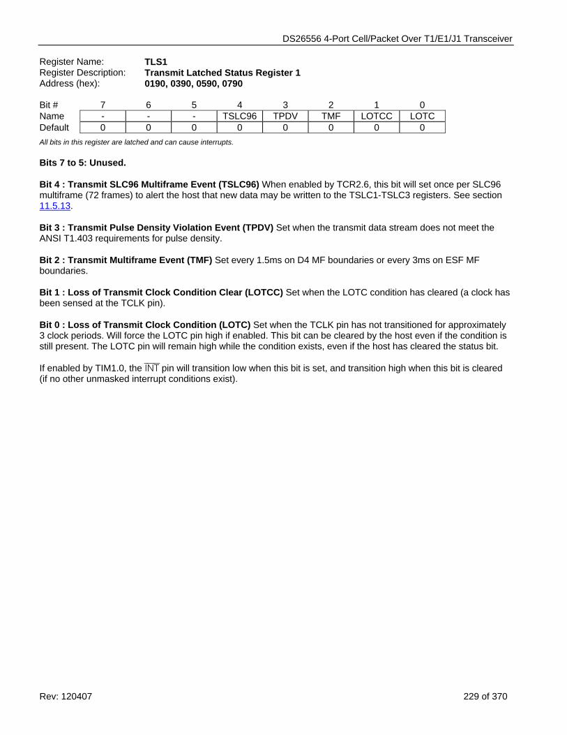
DS26556 4-Port Cell/Packet Over T1/E1/J1 Transceiver
Rev: 120407 229 of 370
Register Name: TLS1 Register Description: Transmit Latched Status Register 1 Address (hex): 0190, 0390, 0590, 0790 Bit # 7 6 5 4 3 2 1 0 Name - - - TSLC96 TPDV TMF LOTCC LOTC Default 0 0 0 0 0 0 0 0 All bits in this register are latched and can cause interrupts. Bits 7 to 5: Unused. Bit 4 : Transmit SLC96 Multiframe Event (TSLC96) When enabled by TCR2.6, this bit will set once per SLC96 multiframe (72 frames) to alert the host that new data may be written to the TSLC1-TSLC3 registers. See section 11.5.13. Bit 3 : Transmit Pulse Density Violation Event (TPDV) Set when the transmit data stream does not meet the ANSI T1.403 requirements for pulse density. Bit 2 : Transmit Multiframe Event (TMF) Set every 1.5ms on D4 MF boundaries or every 3ms on ESF MF boundaries. Bit 1 : Loss of Transmit Clock Condition Clear (LOTCC) Set when the LOTC condition has cleared (a clock has been sensed at the TCLK pin). Bit 0 : Loss of Transmit Clock Condition (LOTC) Set when the TCLK pin has not transitioned for approximately 3 clock periods. Will force the LOTC pin high if enabled. This bit can be cleared by the host even if the condition is still present. The LOTC pin will remain high while the condition exists, even if the host has cleared the status bit. If enabled by TIM1.0, the INT pin will transition low when this bit is set, and transition high when this bit is cleared (if no other unmasked interrupt conditions exist).
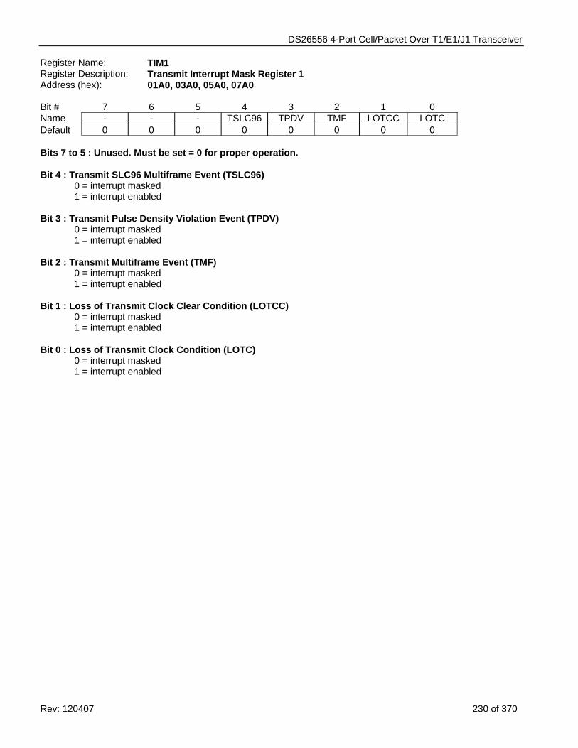
DS26556 4-Port Cell/Packet Over T1/E1/J1 Transceiver
Rev: 120407 230 of 370
Register Name: TIM1 Register Description: Transmit Interrupt Mask Register 1 Address (hex): 01A0, 03A0, 05A0, 07A0 Bit # 7 6 5 4 3 2 1 0 Name - - - TSLC96 TPDV TMF LOTCC LOTC Default 0 0 0 0 0 0 0 0 Bits 7 to 5 : Unused. Must be set = 0 for proper operation. Bit 4 : Transmit SLC96 Multiframe Event (TSLC96)
0 = interrupt masked 1 = interrupt enabled
Bit 3 : Transmit Pulse Density Violation Event (TPDV)
0 = interrupt masked 1 = interrupt enabled
Bit 2 : Transmit Multiframe Event (TMF)
0 = interrupt masked 1 = interrupt enabled
Bit 1 : Loss of Transmit Clock Clear Condition (LOTCC)
0 = interrupt masked 1 = interrupt enabled
Bit 0 : Loss of Transmit Clock Condition (LOTC)
0 = interrupt masked 1 = interrupt enabled
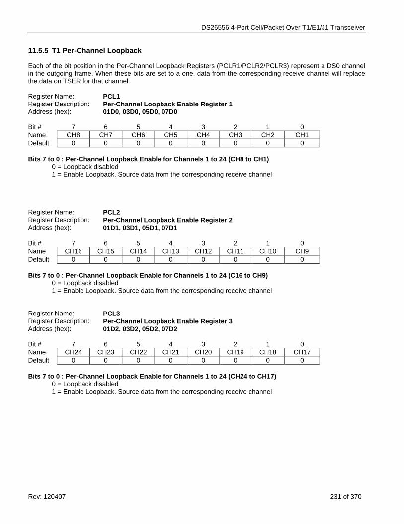
DS26556 4-Port Cell/Packet Over T1/E1/J1 Transceiver
Rev: 120407 231 of 370
11.5.5 T1 Per-Channel Loopback
Each of the bit position in the Per-Channel Loopback Registers (PCLR1/PCLR2/PCLR3) represent a DS0 channel in the outgoing frame. When these bits are set to a one, data from the corresponding receive channel will replace the data on TSER for that channel. Register Name: PCL1 Register Description: Per-Channel Loopback Enable Register 1 Address (hex): 01D0, 03D0, 05D0, 07D0 Bit # 7 6 5 4 3 2 1 0 Name CH8 CH7 CH6 CH5 CH4 CH3 CH2 CH1 Default 0 0 0 0 0 0 0 0 Bits 7 to 0 : Per-Channel Loopback Enable for Channels 1 to 24 (CH8 to CH1)
0 = Loopback disabled 1 = Enable Loopback. Source data from the corresponding receive channel
Register Name: PCL2 Register Description: Per-Channel Loopback Enable Register 2 Address (hex): 01D1, 03D1, 05D1, 07D1 Bit # 7 6 5 4 3 2 1 0 Name CH16 CH15 CH14 CH13 CH12 CH11 CH10 CH9 Default 0 0 0 0 0 0 0 0 Bits 7 to 0 : Per-Channel Loopback Enable for Channels 1 to 24 (C16 to CH9)
0 = Loopback disabled 1 = Enable Loopback. Source data from the corresponding receive channel
Register Name: PCL3 Register Description: Per-Channel Loopback Enable Register 3 Address (hex): 01D2, 03D2, 05D2, 07D2 Bit # 7 6 5 4 3 2 1 0 Name CH24 CH23 CH22 CH21 CH20 CH19 CH18 CH17 Default 0 0 0 0 0 0 0 0 Bits 7 to 0 : Per-Channel Loopback Enable for Channels 1 to 24 (CH24 to CH17)
0 = Loopback disabled 1 = Enable Loopback. Source data from the corresponding receive channel
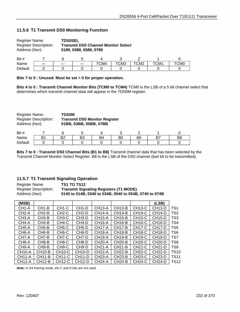
DS26556 4-Port Cell/Packet Over T1/E1/J1 Transceiver
Rev: 120407 232 of 370
11.5.6 T1 Transmit DS0 Monitoring Function
Register Name: TDS0SEL Register Description: Transmit DS0 Channel Monitor Select Address (hex): 0189, 0389, 0589, 0789 Bit # 7 6 5 4 3 2 1 0 Name — — — TCM4 TCM3 TCM2 TCM1 TCM0 Default 0 0 0 0 0 0 0 0 Bits 7 to 5 : Unused. Must be set = 0 for proper operation. Bits 4 to 0 : Transmit Channel Monitor Bits (TCM0 to TCM4) TCM0 is the LSB of a 5 bit channel select that determines which transmit channel data will appear in the TDS0M register. Register Name: TDS0M Register Description: Transmit DS0 Monitor Register Address (hex): 01BB, 03BB, 05BB, 07BB Bit # 7 6 5 4 3 2 1 0 Name B1 B2 B3 B4 B5 B6 B7 B8 Default 0 0 0 0 0 0 0 0 Bits 7 to 0 : Transmit DS0 Channel Bits (B1 to B8) Transmit channel data that has been selected by the Transmit Channel Monitor Select Register. B8 is the LSB of the DS0 channel (last bit to be transmitted).
11.5.7 T1 Transmit Signaling Operation Register Name: TS1 TO TS12 Register Description: Transmit Signaling Registers (T1 MODE) Address (hex): 0140 to 014B, 0340 to 034B, 0540 to 054B, 0740 to 074B (MSB) (LSB) CH1-A CH1-B CH1-C CH1-D CH13-A CH13-B CH13-C CH13-D TS1 CH2-A CH2-B CH2-C CH2-D CH14-A CH14-B CH14-C CH14-D TS2 CH3-A CH3-B CH3-C CH3-D CH15-A CH15-B CH15-C CH15-D TS3 CH4-A CH4-B CH4-C CH4-D CH16-A CH16-B CH16-C CH16-D TS4 CH5-A CH5-B CH5-C CH5-D CH17-A CH17-B CH17-C CH17-D TS5 CH6-A CH6-B CH6-C CH6-D CH18-A CH18-B CH18-C CH18-D TS6 CH7-A CH7-B CH7-C CH7-D CH19-A CH19-B CH19-C CH19-D TS7 CH8-A CH8-B CH8-C CH8-D CH20-A CH20-B CH20-C CH20-D TS8 CH9-A CH9-B CH9-C CH9-D CH21-A CH21-B CH21-C CH21-D TS9
CH10-A CH10-B CH10-C CH10-D CH22-A CH22-B CH22-C CH22-D TS10 CH11-A CH11-B CH11-C CH11-D CH23-A CH23-B CH23-C CH23-D TS11 CH12-A CH12-B CH12-C CH12-D CH24-A CH24-B CH24-C CH24-D TS12 Note: In D4 framing mode, the C and D bits are not used.
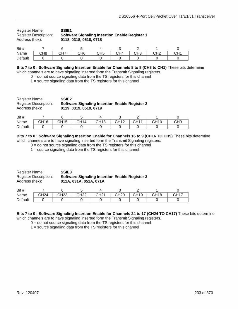
DS26556 4-Port Cell/Packet Over T1/E1/J1 Transceiver
Rev: 120407 233 of 370
Register Name: SSIE1 Register Description: Software Signaling Insertion Enable Register 1 Address (hex): 0118, 0318, 0518, 0718 Bit # 7 6 5 4 3 2 1 0 Name CH8 CH7 CH6 CH5 CH4 CH3 CH2 CH1 Default 0 0 0 0 0 0 0 0 Bits 7 to 0 : Software Signaling Insertion Enable for Channels 8 to 8 (CH8 to CH1) These bits determine which channels are to have signaling inserted form the Transmit Signaling registers.
0 = do not source signaling data from the TS registers for this channel 1 = source signaling data from the TS registers for this channel
Register Name: SSIE2 Register Description: Software Signaling Insertion Enable Register 2 Address (hex): 0119, 0319, 0519, 0719 Bit # 7 6 5 4 3 2 1 0 Name CH16 CH15 CH14 CH13 CH12 CH11 CH10 CH9 Default 0 0 0 0 0 0 0 0 Bits 7 to 0 : Software Signaling Insertion Enable for Channels 16 to 9 (CH16 TO CH9) These bits determine which channels are to have signaling inserted form the Transmit Signaling registers.
0 = do not source signaling data from the TS registers for this channel 1 = source signaling data from the TS registers for this channel
Register Name: SSIE3 Register Description: Software Signaling Insertion Enable Register 3 Address (hex): 011A, 031A, 051A, 071A Bit # 7 6 5 4 3 2 1 0 Name CH24 CH23 CH22 CH21 CH20 CH19 CH18 CH17 Default 0 0 0 0 0 0 0 0 Bits 7 to 0 : Software Signaling Insertion Enable for Channels 24 to 17 (CH24 TO CH17) These bits determine which channels are to have signaling inserted form the Transmit Signaling registers.
0 = do not source signaling data from the TS registers for this channel 1 = source signaling data from the TS registers for this channel
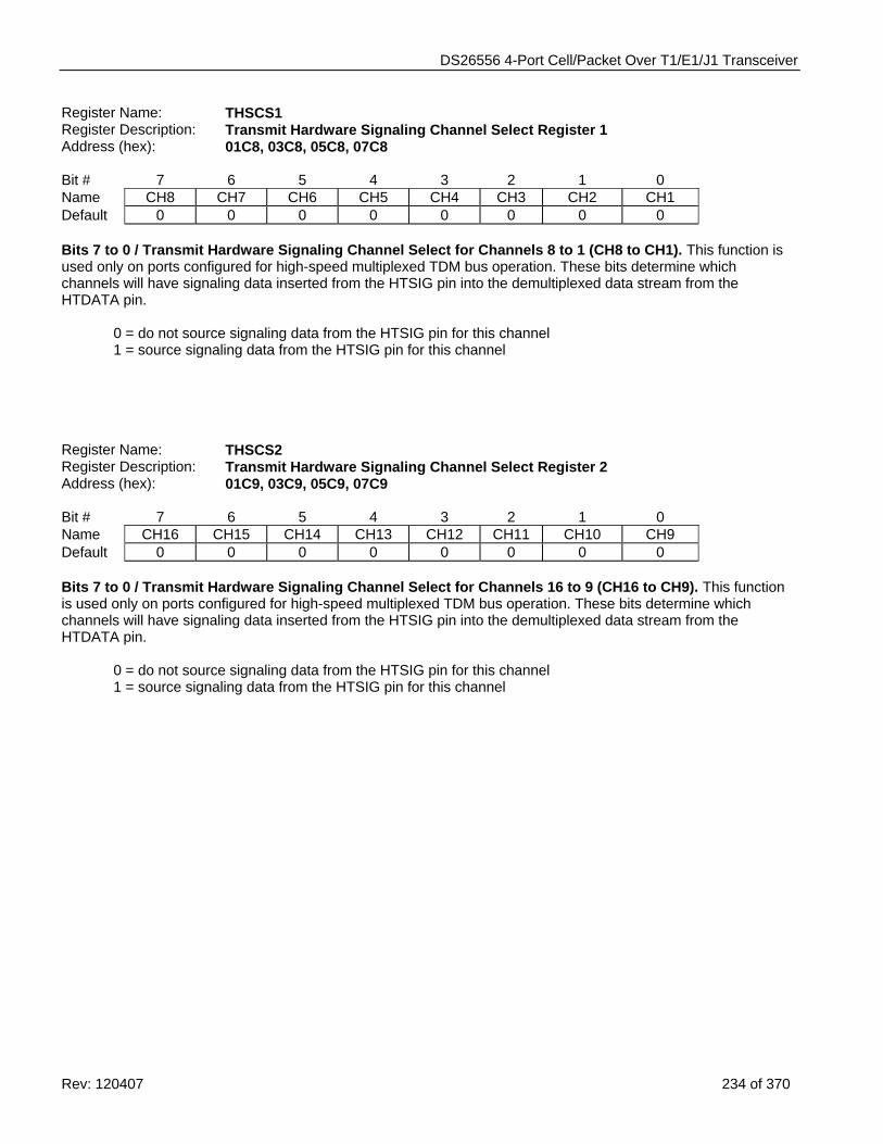
DS26556 4-Port Cell/Packet Over T1/E1/J1 Transceiver
Rev: 120407 234 of 370
Register Name: THSCS1 Register Description: Transmit Hardware Signaling Channel Select Register 1 Address (hex): 01C8, 03C8, 05C8, 07C8 Bit # 7 6 5 4 3 2 1 0 Name CH8 CH7 CH6 CH5 CH4 CH3 CH2 CH1 Default 0 0 0 0 0 0 0 0 Bits 7 to 0 / Transmit Hardware Signaling Channel Select for Channels 8 to 1 (CH8 to CH1). This function is used only on ports configured for high-speed multiplexed TDM bus operation. These bits determine which channels will have signaling data inserted from the HTSIG pin into the demultiplexed data stream from the HTDATA pin.
0 = do not source signaling data from the HTSIG pin for this channel 1 = source signaling data from the HTSIG pin for this channel
Register Name: THSCS2 Register Description: Transmit Hardware Signaling Channel Select Register 2 Address (hex): 01C9, 03C9, 05C9, 07C9 Bit # 7 6 5 4 3 2 1 0 Name CH16 CH15 CH14 CH13 CH12 CH11 CH10 CH9 Default 0 0 0 0 0 0 0 0 Bits 7 to 0 / Transmit Hardware Signaling Channel Select for Channels 16 to 9 (CH16 to CH9). This function is used only on ports configured for high-speed multiplexed TDM bus operation. These bits determine which channels will have signaling data inserted from the HTSIG pin into the demultiplexed data stream from the HTDATA pin.
0 = do not source signaling data from the HTSIG pin for this channel 1 = source signaling data from the HTSIG pin for this channel

DS26556 4-Port Cell/Packet Over T1/E1/J1 Transceiver
Rev: 120407 235 of 370
Register Name: THSCS3 Register Description: Transmit Hardware Signaling Channel Select Register 3 Address (hex): 01CA, 03CA, 05CA, 07CA Bit # 7 6 5 4 3 2 1 0 Name CH24 CH23 CH22 CH21 CH20 CH19 CH18 CH17 Default 0 0 0 0 0 0 0 0 Bits 7 to 0 / Transmit Hardware Signaling Channel Select for Channels 24 to 17 (CH24 to CH17 This function is used only on ports configured for high-speed multiplexed TDM bus operation. These bits determine which channels will have signaling data inserted from the HTSIG pin into the demultiplexed data stream from the HTDATA pin.
0 = do not source signaling data from the HTSIG pin for this channel 1 = source signaling data from the HTSIG pin for this channel
Register Name: THSCS4 Register Description: Transmit Hardware Signaling Channel Select Register 4 Address (hex): 01CB, 03CB, 05CB, 07CB Bit # 7 6 5 4 3 2 1 0 Name CH32 CH31 CH30 CH29 CH28 CH27 CH26 CH25 Default 0 0 0 0 0 0 0 0 Bits 7 to 0 / Transmit Hardware Signaling Channel Select for Channels 32 to 25 (CH32 to CH25). This function is used only on ports configured for high-speed multiplexed TDM bus operation. These bits determine which channels will have signaling data inserted from the HTSIG pin into the demultiplexed data stream from the HTDATA pin.
0 = do not source signaling data from the HTSIG pin for this channel 1 = source signaling data from the HTSIG pin for this channel
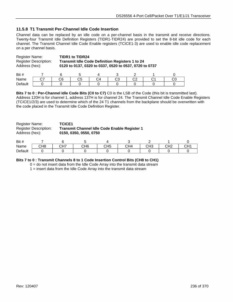
DS26556 4-Port Cell/Packet Over T1/E1/J1 Transceiver
Rev: 120407 236 of 370
11.5.8 T1 Transmit Per-Channel Idle Code Insertion Channel data can be replaced by an idle code on a per-channel basis in the transmit and receive directions. Twenty-four Transmit Idle Definition Registers (TIDR1-TIDR24) are provided to set the 8-bit idle code for each channel. The Transmit Channel Idle Code Enable registers (TCICE1-3) are used to enable idle code replacement on a per channel basis. Register Name: TIDR1 to TIDR24 Register Description: Transmit Idle Code Definition Registers 1 to 24 Address (hex): 0120 to 0137, 0320 to 0337, 0520 to 0537, 0720 to 0737 Bit # 7 6 5 4 3 2 1 0 Name C7 C6 C5 C4 C3 C2 C1 C0 Default 0 0 0 0 0 0 0 0 Bits 7 to 0 : Per-Channel Idle Code Bits (C0 to C7) C0 is the LSB of the Code (this bit is transmitted last). Address 120H is for channel 1, address 137H is for channel 24. The Transmit Channel Idle Code Enable Registers (TCICE1/2/3) are used to determine which of the 24 T1 channels from the backplane should be overwritten with the code placed in the Transmit Idle Code Definition Register. Register Name: TCICE1 Register Description: Transmit Channel Idle Code Enable Register 1 Address (hex): 0150, 0350, 0550, 0750 Bit # 7 6 5 4 3 2 1 0 Name CH8 CH7 CH6 CH5 CH4 CH3 CH2 CH1 Default 0 0 0 0 0 0 0 0 Bits 7 to 0 : Transmit Channels 8 to 1 Code Insertion Control Bits (CH8 to CH1)
0 = do not insert data from the Idle Code Array into the transmit data stream 1 = insert data from the Idle Code Array into the transmit data stream
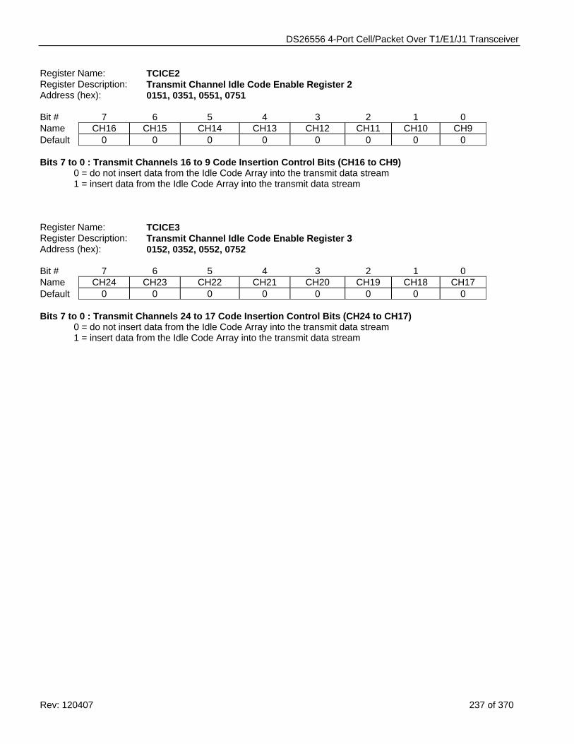
DS26556 4-Port Cell/Packet Over T1/E1/J1 Transceiver
Rev: 120407 237 of 370
Register Name: TCICE2 Register Description: Transmit Channel Idle Code Enable Register 2 Address (hex): 0151, 0351, 0551, 0751 Bit # 7 6 5 4 3 2 1 0 Name CH16 CH15 CH14 CH13 CH12 CH11 CH10 CH9 Default 0 0 0 0 0 0 0 0 Bits 7 to 0 : Transmit Channels 16 to 9 Code Insertion Control Bits (CH16 to CH9)
0 = do not insert data from the Idle Code Array into the transmit data stream 1 = insert data from the Idle Code Array into the transmit data stream
Register Name: TCICE3 Register Description: Transmit Channel Idle Code Enable Register 3 Address (hex): 0152, 0352, 0552, 0752 Bit # 7 6 5 4 3 2 1 0 Name CH24 CH23 CH22 CH21 CH20 CH19 CH18 CH17 Default 0 0 0 0 0 0 0 0 Bits 7 to 0 : Transmit Channels 24 to 17 Code Insertion Control Bits (CH24 to CH17)
0 = do not insert data from the Idle Code Array into the transmit data stream 1 = insert data from the Idle Code Array into the transmit data stream
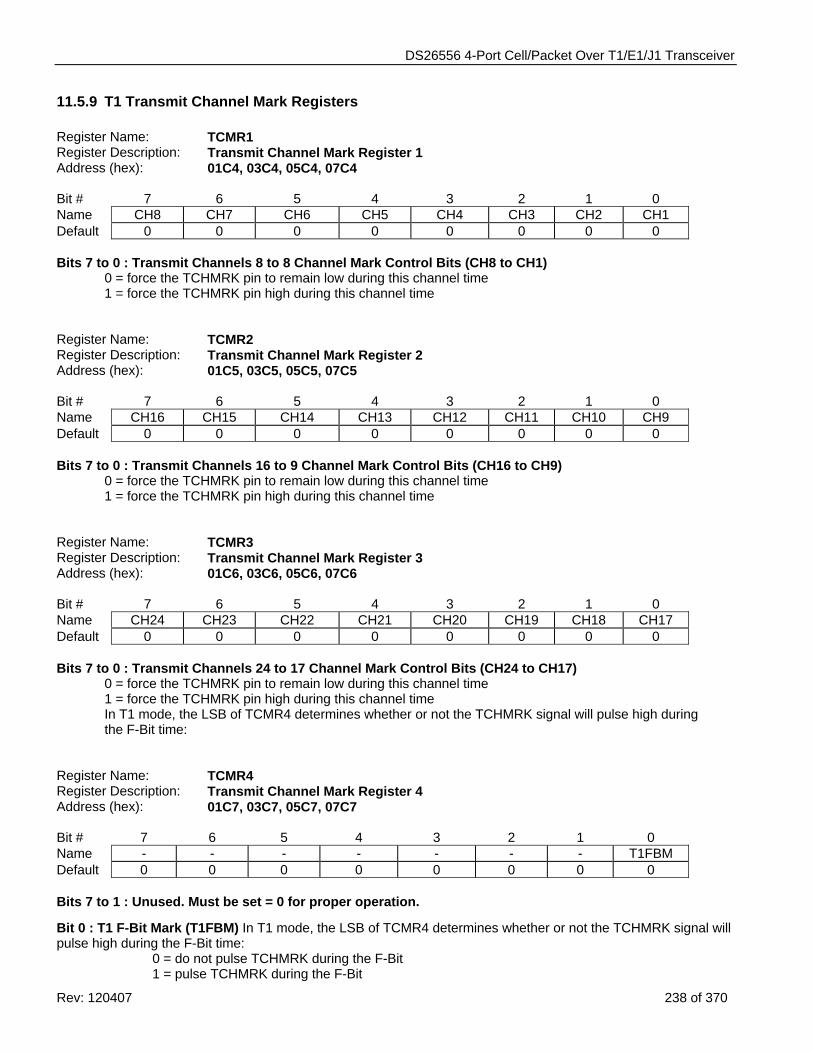
DS26556 4-Port Cell/Packet Over T1/E1/J1 Transceiver
Rev: 120407 238 of 370
11.5.9 T1 Transmit Channel Mark Registers Register Name: TCMR1 Register Description: Transmit Channel Mark Register 1 Address (hex): 01C4, 03C4, 05C4, 07C4 Bit # 7 6 5 4 3 2 1 0 Name CH8 CH7 CH6 CH5 CH4 CH3 CH2 CH1 Default 0 0 0 0 0 0 0 0 Bits 7 to 0 : Transmit Channels 8 to 8 Channel Mark Control Bits (CH8 to CH1)
0 = force the TCHMRK pin to remain low during this channel time 1 = force the TCHMRK pin high during this channel time
Register Name: TCMR2 Register Description: Transmit Channel Mark Register 2 Address (hex): 01C5, 03C5, 05C5, 07C5 Bit # 7 6 5 4 3 2 1 0 Name CH16 CH15 CH14 CH13 CH12 CH11 CH10 CH9 Default 0 0 0 0 0 0 0 0 Bits 7 to 0 : Transmit Channels 16 to 9 Channel Mark Control Bits (CH16 to CH9)
0 = force the TCHMRK pin to remain low during this channel time 1 = force the TCHMRK pin high during this channel time
Register Name: TCMR3 Register Description: Transmit Channel Mark Register 3 Address (hex): 01C6, 03C6, 05C6, 07C6 Bit # 7 6 5 4 3 2 1 0 Name CH24 CH23 CH22 CH21 CH20 CH19 CH18 CH17 Default 0 0 0 0 0 0 0 0 Bits 7 to 0 : Transmit Channels 24 to 17 Channel Mark Control Bits (CH24 to CH17)
0 = force the TCHMRK pin to remain low during this channel time 1 = force the TCHMRK pin high during this channel time In T1 mode, the LSB of TCMR4 determines whether or not the TCHMRK signal will pulse high during the F-Bit time:
Register Name: TCMR4 Register Description: Transmit Channel Mark Register 4 Address (hex): 01C7, 03C7, 05C7, 07C7 Bit # 7 6 5 4 3 2 1 0 Name - - - - - - - T1FBM Default 0 0 0 0 0 0 0 0 Bits 7 to 1 : Unused. Must be set = 0 for proper operation.
Bit 0 : T1 F-Bit Mark (T1FBM) In T1 mode, the LSB of TCMR4 determines whether or not the TCHMRK signal will pulse high during the F-Bit time:
0 = do not pulse TCHMRK during the F-Bit 1 = pulse TCHMRK during the F-Bit
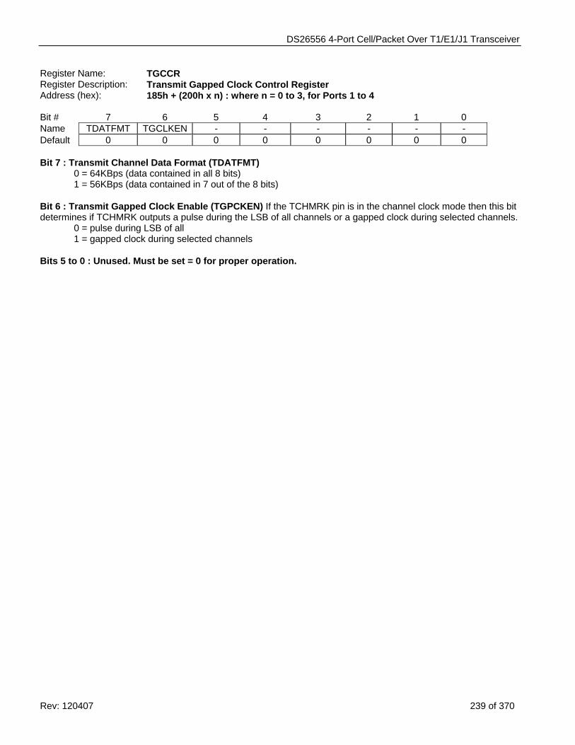
DS26556 4-Port Cell/Packet Over T1/E1/J1 Transceiver
Rev: 120407 239 of 370
Register Name: TGCCR Register Description: Transmit Gapped Clock Control Register Address (hex): 185h + (200h x n) : where n = 0 to 3, for Ports 1 to 4 Bit # 7 6 5 4 3 2 1 0 Name TDATFMT TGCLKEN - - - - - - Default 0 0 0 0 0 0 0 0 Bit 7 : Transmit Channel Data Format (TDATFMT)
0 = 64KBps (data contained in all 8 bits) 1 = 56KBps (data contained in 7 out of the 8 bits)
Bit 6 : Transmit Gapped Clock Enable (TGPCKEN) If the TCHMRK pin is in the channel clock mode then this bit determines if TCHMRK outputs a pulse during the LSB of all channels or a gapped clock during selected channels.
0 = pulse during LSB of all 1 = gapped clock during selected channels
Bits 5 to 0 : Unused. Must be set = 0 for proper operation.
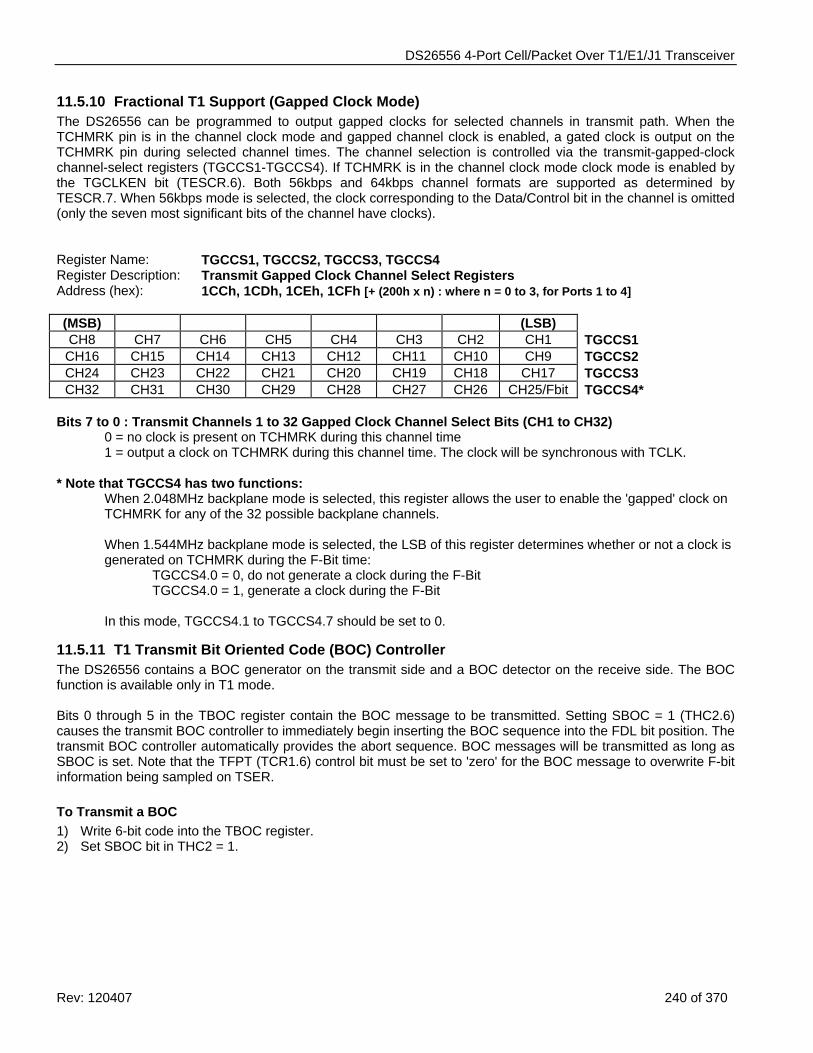
DS26556 4-Port Cell/Packet Over T1/E1/J1 Transceiver
Rev: 120407 240 of 370
11.5.10 Fractional T1 Support (Gapped Clock Mode) The DS26556 can be programmed to output gapped clocks for selected channels in transmit path. When the TCHMRK pin is in the channel clock mode and gapped channel clock is enabled, a gated clock is output on the TCHMRK pin during selected channel times. The channel selection is controlled via the transmit-gapped-clock channel-select registers (TGCCS1-TGCCS4). If TCHMRK is in the channel clock mode clock mode is enabled by the TGCLKEN bit (TESCR.6). Both 56kbps and 64kbps channel formats are supported as determined by TESCR.7. When 56kbps mode is selected, the clock corresponding to the Data/Control bit in the channel is omitted (only the seven most significant bits of the channel have clocks). Register Name: TGCCS1, TGCCS2, TGCCS3, TGCCS4 Register Description: Transmit Gapped Clock Channel Select Registers Address (hex): 1CCh, 1CDh, 1CEh, 1CFh [+ (200h x n) : where n = 0 to 3, for Ports 1 to 4] (MSB) (LSB) CH8 CH7 CH6 CH5 CH4 CH3 CH2 CH1 TGCCS1 CH16 CH15 CH14 CH13 CH12 CH11 CH10 CH9 TGCCS2 CH24 CH23 CH22 CH21 CH20 CH19 CH18 CH17 TGCCS3 CH32 CH31 CH30 CH29 CH28 CH27 CH26 CH25/Fbit TGCCS4*
Bits 7 to 0 : Transmit Channels 1 to 32 Gapped Clock Channel Select Bits (CH1 to CH32)
0 = no clock is present on TCHMRK during this channel time 1 = output a clock on TCHMRK during this channel time. The clock will be synchronous with TCLK.
* Note that TGCCS4 has two functions:
When 2.048MHz backplane mode is selected, this register allows the user to enable the 'gapped' clock on TCHMRK for any of the 32 possible backplane channels. When 1.544MHz backplane mode is selected, the LSB of this register determines whether or not a clock is generated on TCHMRK during the F-Bit time:
TGCCS4.0 = 0, do not generate a clock during the F-Bit TGCCS4.0 = 1, generate a clock during the F-Bit
In this mode, TGCCS4.1 to TGCCS4.7 should be set to 0.
11.5.11 T1 Transmit Bit Oriented Code (BOC) Controller The DS26556 contains a BOC generator on the transmit side and a BOC detector on the receive side. The BOC function is available only in T1 mode. Bits 0 through 5 in the TBOC register contain the BOC message to be transmitted. Setting SBOC = 1 (THC2.6) causes the transmit BOC controller to immediately begin inserting the BOC sequence into the FDL bit position. The transmit BOC controller automatically provides the abort sequence. BOC messages will be transmitted as long as SBOC is set. Note that the TFPT (TCR1.6) control bit must be set to 'zero' for the BOC message to overwrite F-bit information being sampled on TSER. To Transmit a BOC 1) Write 6-bit code into the TBOC register. 2) Set SBOC bit in THC2 = 1.
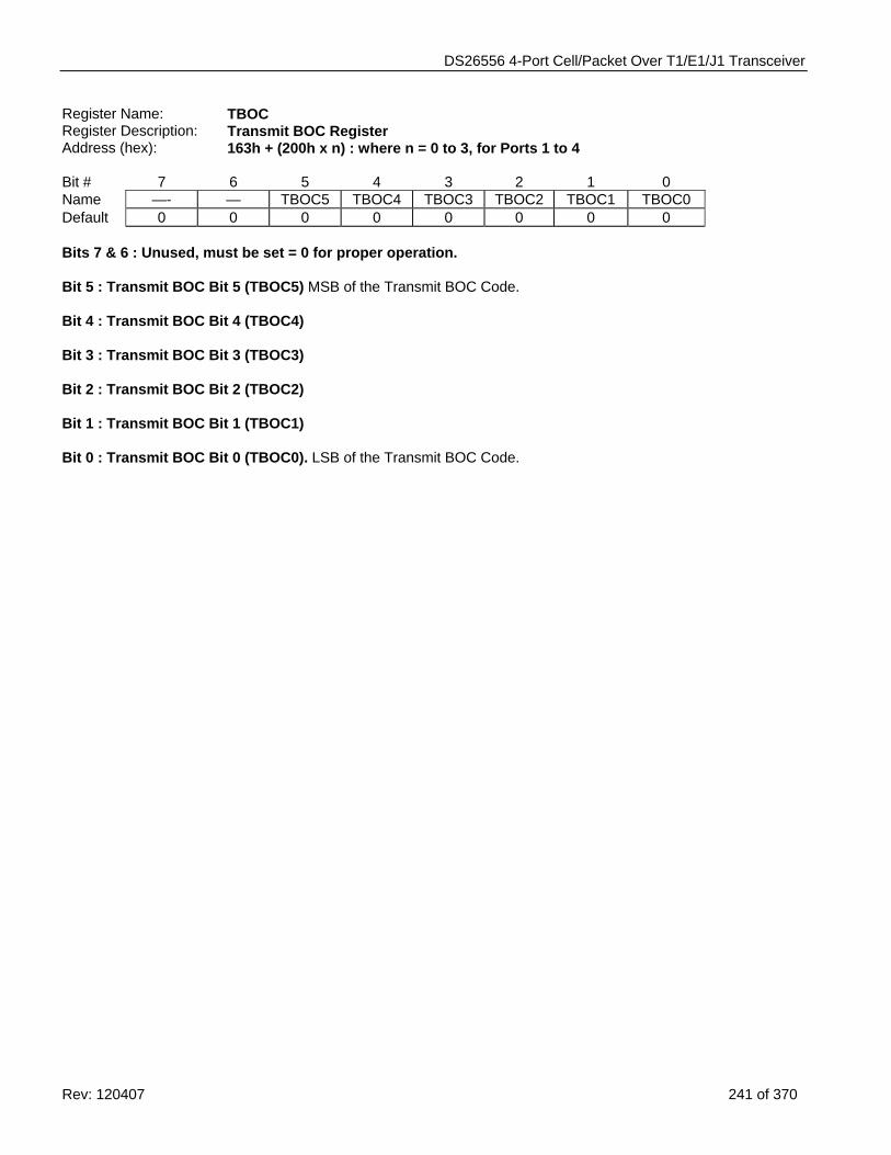
DS26556 4-Port Cell/Packet Over T1/E1/J1 Transceiver
Rev: 120407 241 of 370
Register Name: TBOC Register Description: Transmit BOC Register Address (hex): 163h + (200h x n) : where n = 0 to 3, for Ports 1 to 4 Bit # 7 6 5 4 3 2 1 0 Name —- — TBOC5 TBOC4 TBOC3 TBOC2 TBOC1 TBOC0 Default 0 0 0 0 0 0 0 0 Bits 7 & 6 : Unused, must be set = 0 for proper operation. Bit 5 : Transmit BOC Bit 5 (TBOC5) MSB of the Transmit BOC Code. Bit 4 : Transmit BOC Bit 4 (TBOC4) Bit 3 : Transmit BOC Bit 3 (TBOC3) Bit 2 : Transmit BOC Bit 2 (TBOC2) Bit 1 : Transmit BOC Bit 1 (TBOC1) Bit 0 : Transmit BOC Bit 0 (TBOC0). LSB of the Transmit BOC Code.
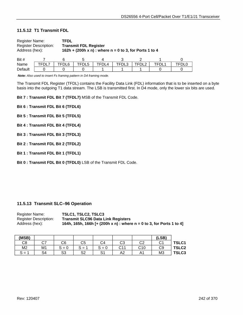
DS26556 4-Port Cell/Packet Over T1/E1/J1 Transceiver
Rev: 120407 242 of 370
11.5.12 T1 Transmit FDL Register Name: TFDL Register Description: Transmit FDL Register Address (hex): 162h + (200h x n) : where n = 0 to 3, for Ports 1 to 4 Bit # 7 6 5 4 3 2 1 0 Name TFDL7 TFDL6 TFDL5 TFDL4 TFDL3 TFDL2 TFDL1 TFDL0 Default 0 0 0 1 1 1 0 0 Note: Also used to insert Fs framing pattern in D4 framing mode. The Transmit FDL Register (TFDL) contains the Facility Data Link (FDL) information that is to be inserted on a byte basis into the outgoing T1 data stream. The LSB is transmitted first. In D4 mode, only the lower six bits are used. Bit 7 : Transmit FDL Bit 7 (TFDL7) MSB of the Transmit FDL Code. Bit 6 : Transmit FDL Bit 6 (TFDL6) Bit 5 : Transmit FDL Bit 5 (TFDL5) Bit 4 : Transmit FDL Bit 4 (TFDL4) Bit 3 : Transmit FDL Bit 3 (TFDL3) Bit 2 : Transmit FDL Bit 2 (TFDL2) Bit 1 : Transmit FDL Bit 1 (TFDL1) Bit 0 : Transmit FDL Bit 0 (TFDL0) LSB of the Transmit FDL Code.
11.5.13 Transmit SLC–96 Operation Register Name: TSLC1, TSLC2, TSLC3 Register Description: Transmit SLC96 Data Link Registers Address (hex): 164h, 165h, 166h [+ (200h x n) : where n = 0 to 3, for Ports 1 to 4] (MSB) (LSB)
C8 C7 C6 C5 C4 C3 C2 C1 TSLC1 M2 M1 S = 0 S = 1 S = 0 C11 C10 C9 TSLC2
S = 1 S4 S3 S2 S1 A2 A1 M3 TSLC3
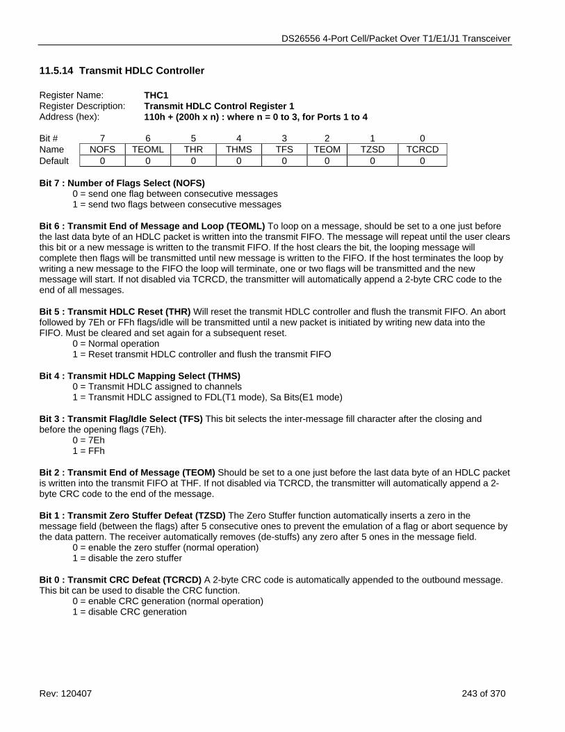
DS26556 4-Port Cell/Packet Over T1/E1/J1 Transceiver
Rev: 120407 243 of 370
11.5.14 Transmit HDLC Controller Register Name: THC1 Register Description: Transmit HDLC Control Register 1 Address (hex): 110h + (200h x n) : where n = 0 to 3, for Ports 1 to 4 Bit # 7 6 5 4 3 2 1 0 Name NOFS TEOML THR THMS TFS TEOM TZSD TCRCD Default 0 0 0 0 0 0 0 0 Bit 7 : Number of Flags Select (NOFS) 0 = send one flag between consecutive messages 1 = send two flags between consecutive messages Bit 6 : Transmit End of Message and Loop (TEOML) To loop on a message, should be set to a one just before the last data byte of an HDLC packet is written into the transmit FIFO. The message will repeat until the user clears this bit or a new message is written to the transmit FIFO. If the host clears the bit, the looping message will complete then flags will be transmitted until new message is written to the FIFO. If the host terminates the loop by writing a new message to the FIFO the loop will terminate, one or two flags will be transmitted and the new message will start. If not disabled via TCRCD, the transmitter will automatically append a 2-byte CRC code to the end of all messages. Bit 5 : Transmit HDLC Reset (THR) Will reset the transmit HDLC controller and flush the transmit FIFO. An abort followed by 7Eh or FFh flags/idle will be transmitted until a new packet is initiated by writing new data into the FIFO. Must be cleared and set again for a subsequent reset. 0 = Normal operation 1 = Reset transmit HDLC controller and flush the transmit FIFO Bit 4 : Transmit HDLC Mapping Select (THMS)
0 = Transmit HDLC assigned to channels 1 = Transmit HDLC assigned to FDL(T1 mode), Sa Bits(E1 mode)
Bit 3 : Transmit Flag/Idle Select (TFS) This bit selects the inter-message fill character after the closing and before the opening flags (7Eh).
0 = 7Eh 1 = FFh
Bit 2 : Transmit End of Message (TEOM) Should be set to a one just before the last data byte of an HDLC packet is written into the transmit FIFO at THF. If not disabled via TCRCD, the transmitter will automatically append a 2-byte CRC code to the end of the message. Bit 1 : Transmit Zero Stuffer Defeat (TZSD) The Zero Stuffer function automatically inserts a zero in the message field (between the flags) after 5 consecutive ones to prevent the emulation of a flag or abort sequence by the data pattern. The receiver automatically removes (de-stuffs) any zero after 5 ones in the message field.
0 = enable the zero stuffer (normal operation) 1 = disable the zero stuffer
Bit 0 : Transmit CRC Defeat (TCRCD) A 2-byte CRC code is automatically appended to the outbound message. This bit can be used to disable the CRC function.
0 = enable CRC generation (normal operation) 1 = disable CRC generation
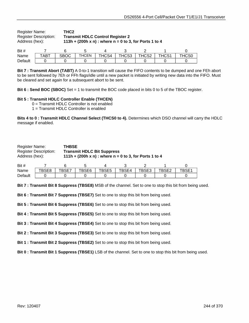
DS26556 4-Port Cell/Packet Over T1/E1/J1 Transceiver
Rev: 120407 244 of 370
Register Name: THC2 Register Description: Transmit HDLC Control Register 2 Address (hex): 113h + (200h x n) : where n = 0 to 3, for Ports 1 to 4 Bit # 7 6 5 4 3 2 1 0 Name TABT SBOC THCEN THCS4 THCS3 THCS2 THCS1 THCS0 Default 0 0 0 0 0 0 0 0 Bit 7 : Transmit Abort (TABT) A 0-to-1 transition will cause the FIFO contents to be dumped and one FEh abort to be sent followed by 7Eh or FFh flags/idle until a new packet is initiated by writing new data into the FIFO. Must be cleared and set again for a subsequent abort to be sent. Bit 6 : Send BOC (SBOC) Set = 1 to transmit the BOC code placed in bits 0 to 5 of the TBOC register. Bit 5 : Transmit HDLC Controller Enable (THCEN) 0 = Transmit HDLC Controller is not enabled 1 = Transmit HDLC Controller is enabled Bits 4 to 0 : Transmit HDLC Channel Select (THCS0 to 4). Determines which DSO channel will carry the HDLC message if enabled. Register Name: THBSE Register Description: Transmit HDLC Bit Suppress Address (hex): 111h + (200h x n) : where n = 0 to 3, for Ports 1 to 4 Bit # 7 6 5 4 3 2 1 0 Name TBSE8 TBSE7 TBSE6 TBSE5 TBSE4 TBSE3 TBSE2 TBSE1 Default 0 0 0 0 0 0 0 0 Bit 7 : Transmit Bit 8 Suppress (TBSE8) MSB of the channel. Set to one to stop this bit from being used. Bit 6 : Transmit Bit 7 Suppress (TBSE7) Set to one to stop this bit from being used. Bit 5 : Transmit Bit 6 Suppress (TBSE6) Set to one to stop this bit from being used. Bit 4 : Transmit Bit 5 Suppress (TBSE5) Set to one to stop this bit from being used. Bit 3 : Transmit Bit 4 Suppress (TBSE4) Set to one to stop this bit from being used. Bit 2 : Transmit Bit 3 Suppress (TBSE3) Set to one to stop this bit from being used. Bit 1 : Transmit Bit 2 Suppress (TBSE2) Set to one to stop this bit from being used. Bit 0 : Transmit Bit 1 Suppress (TBSE1) LSB of the channel. Set to one to stop this bit from being used.
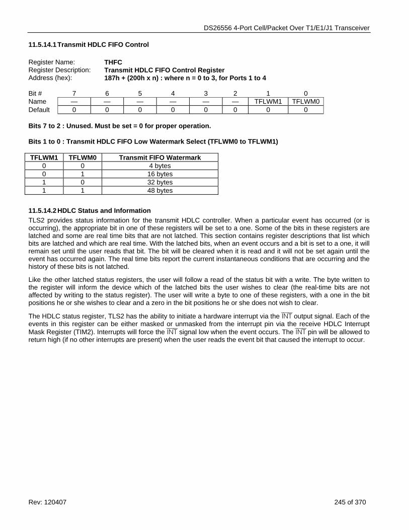
DS26556 4-Port Cell/Packet Over T1/E1/J1 Transceiver
Rev: 120407 245 of 370
11.5.14.1 Transmit HDLC FIFO Control Register Name: THFC Register Description: Transmit HDLC FIFO Control Register Address (hex): 187h + (200h x n) : where n = 0 to 3, for Ports 1 to 4 Bit # 7 6 5 4 3 2 1 0 Name — — — — — — TFLWM1 TFLWM0 Default 0 0 0 0 0 0 0 0 Bits 7 to 2 : Unused. Must be set = 0 for proper operation. Bits 1 to 0 : Transmit HDLC FIFO Low Watermark Select (TFLWM0 to TFLWM1) TFLWM1 TFLWM0 Transmit FIFO Watermark
0 0 4 bytes 0 1 16 bytes 1 0 32 bytes 1 1 48 bytes
11.5.14.2 HDLC Status and Information TLS2 provides status information for the transmit HDLC controller. When a particular event has occurred (or is occurring), the appropriate bit in one of these registers will be set to a one. Some of the bits in these registers are latched and some are real time bits that are not latched. This section contains register descriptions that list which bits are latched and which are real time. With the latched bits, when an event occurs and a bit is set to a one, it will remain set until the user reads that bit. The bit will be cleared when it is read and it will not be set again until the event has occurred again. The real time bits report the current instantaneous conditions that are occurring and the history of these bits is not latched.
Like the other latched status registers, the user will follow a read of the status bit with a write. The byte written to the register will inform the device which of the latched bits the user wishes to clear (the real-time bits are not affected by writing to the status register). The user will write a byte to one of these registers, with a one in the bit positions he or she wishes to clear and a zero in the bit positions he or she does not wish to clear.
The HDLC status register, TLS2 has the ability to initiate a hardware interrupt via the INT output signal. Each of the events in this register can be either masked or unmasked from the interrupt pin via the receive HDLC Interrupt Mask Register (TIM2). Interrupts will force the INT signal low when the event occurs. The INT pin will be allowed to return high (if no other interrupts are present) when the user reads the event bit that caused the interrupt to occur.
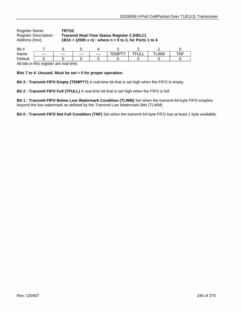
DS26556 4-Port Cell/Packet Over T1/E1/J1 Transceiver
Rev: 120407 246 of 370
Register Name: TRTS2 Register Description: Transmit Real-Time Status Register 2 (HDLC) Address (hex): 1B1h + (200h x n) : where n = 0 to 3, for Ports 1 to 4 Bit # 7 6 5 4 3 2 1 0 Name — — — — TEMPTY TFULL TLWM TNF Default 0 0 0 0 0 0 0 0 All bits in this register are real time. Bits 7 to 4: Unused. Must be set = 0 for proper operation. Bit 3 : Transmit FIFO Empty (TEMPTY) A real-time bit that is set high when the FIFO is empty. Bit 2 : Transmit FIFO Full (TFULL) A real-time bit that is set high when the FIFO is full. Bit 1 : Transmit FIFO Below Low Watermark Condition (TLWM) Set when the transmit 64-byte FIFO empties beyond the low watermark as defined by the Transmit Low Watermark Bits (TLWM). Bit 0 : Transmit FIFO Not Full Condition (TNF) Set when the transmit 64-byte FIFO has at least 1 byte available.
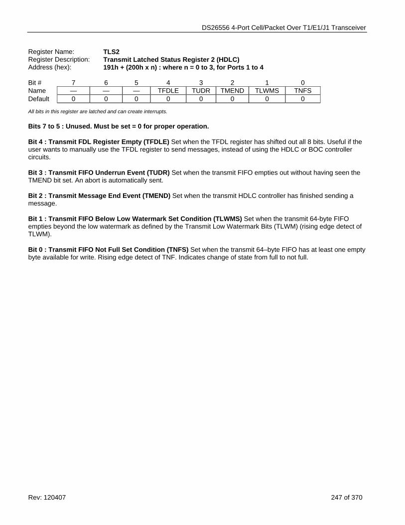
DS26556 4-Port Cell/Packet Over T1/E1/J1 Transceiver
Rev: 120407 247 of 370
Register Name: TLS2 Register Description: Transmit Latched Status Register 2 (HDLC) Address (hex): 191h + (200h x n) : where n = 0 to 3, for Ports 1 to 4 Bit # 7 6 5 4 3 2 1 0 Name — — — TFDLE TUDR TMEND TLWMS TNFS Default 0 0 0 0 0 0 0 0
All bits in this register are latched and can create interrupts. Bits 7 to 5 : Unused. Must be set = 0 for proper operation. Bit 4 : Transmit FDL Register Empty (TFDLE) Set when the TFDL register has shifted out all 8 bits. Useful if the user wants to manually use the TFDL register to send messages, instead of using the HDLC or BOC controller circuits. Bit 3 : Transmit FIFO Underrun Event (TUDR) Set when the transmit FIFO empties out without having seen the TMEND bit set. An abort is automatically sent. Bit 2 : Transmit Message End Event (TMEND) Set when the transmit HDLC controller has finished sending a message. Bit 1 : Transmit FIFO Below Low Watermark Set Condition (TLWMS) Set when the transmit 64-byte FIFO empties beyond the low watermark as defined by the Transmit Low Watermark Bits (TLWM) (rising edge detect of TLWM). Bit 0 : Transmit FIFO Not Full Set Condition (TNFS) Set when the transmit 64–byte FIFO has at least one empty byte available for write. Rising edge detect of TNF. Indicates change of state from full to not full.
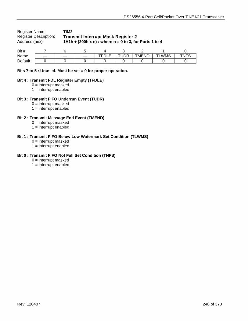
DS26556 4-Port Cell/Packet Over T1/E1/J1 Transceiver
Rev: 120407 248 of 370
Register Name: TIM2 Register Description: Transmit Interrupt Mask Register 2 Address (hex): 1A1h + (200h x n) : where n = 0 to 3, for Ports 1 to 4 Bit # 7 6 5 4 3 2 1 0 Name — — — TFDLE TUDR TMEND TLWMS TNFS Default 0 0 0 0 0 0 0 0 Bits 7 to 5 : Unused. Must be set = 0 for proper operation. Bit 4 : Transmit FDL Register Empty (TFDLE)
0 = interrupt masked 1 = interrupt enabled
Bit 3 : Transmit FIFO Underrun Event (TUDR)
0 = interrupt masked 1 = interrupt enabled
Bit 2 : Transmit Message End Event (TMEND)
0 = interrupt masked 1 = interrupt enabled
Bit 1 : Transmit FIFO Below Low Watermark Set Condition (TLWMS)
0 = interrupt masked 1 = interrupt enabled
Bit 0 : Transmit FIFO Not Full Set Condition (TNFS)
0 = interrupt masked 1 = interrupt enabled
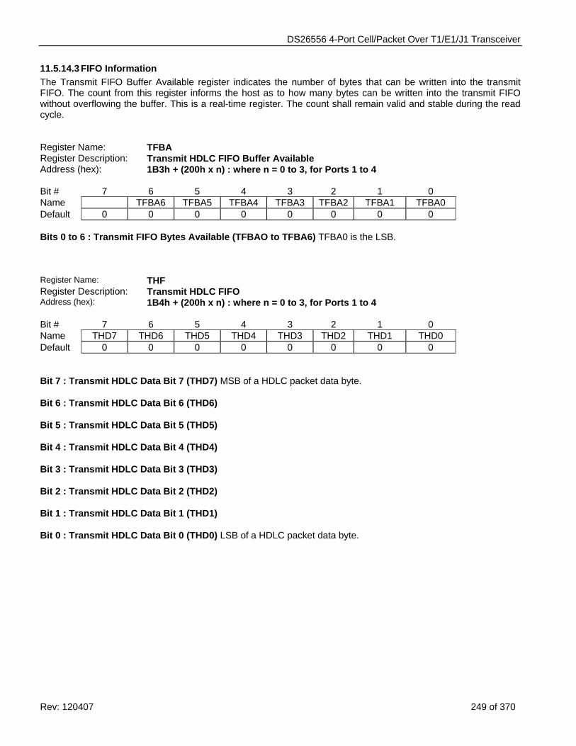
DS26556 4-Port Cell/Packet Over T1/E1/J1 Transceiver
Rev: 120407 249 of 370
11.5.14.3 FIFO Information The Transmit FIFO Buffer Available register indicates the number of bytes that can be written into the transmit FIFO. The count from this register informs the host as to how many bytes can be written into the transmit FIFO without overflowing the buffer. This is a real-time register. The count shall remain valid and stable during the read cycle. Register Name: TFBA Register Description: Transmit HDLC FIFO Buffer Available Address (hex): 1B3h + (200h x n) : where n = 0 to 3, for Ports 1 to 4 Bit # 7 6 5 4 3 2 1 0 Name TFBA6 TFBA5 TFBA4 TFBA3 TFBA2 TFBA1 TFBA0 Default 0 0 0 0 0 0 0 0 Bits 0 to 6 : Transmit FIFO Bytes Available (TFBAO to TFBA6) TFBA0 is the LSB. Register Name: THF Register Description: Transmit HDLC FIFO Address (hex): 1B4h + (200h x n) : where n = 0 to 3, for Ports 1 to 4 Bit # 7 6 5 4 3 2 1 0 Name THD7 THD6 THD5 THD4 THD3 THD2 THD1 THD0 Default 0 0 0 0 0 0 0 0 Bit 7 : Transmit HDLC Data Bit 7 (THD7) MSB of a HDLC packet data byte. Bit 6 : Transmit HDLC Data Bit 6 (THD6) Bit 5 : Transmit HDLC Data Bit 5 (THD5) Bit 4 : Transmit HDLC Data Bit 4 (THD4) Bit 3 : Transmit HDLC Data Bit 3 (THD3) Bit 2 : Transmit HDLC Data Bit 2 (THD2) Bit 1 : Transmit HDLC Data Bit 1 (THD1) Bit 0 : Transmit HDLC Data Bit 0 (THD0) LSB of a HDLC packet data byte.
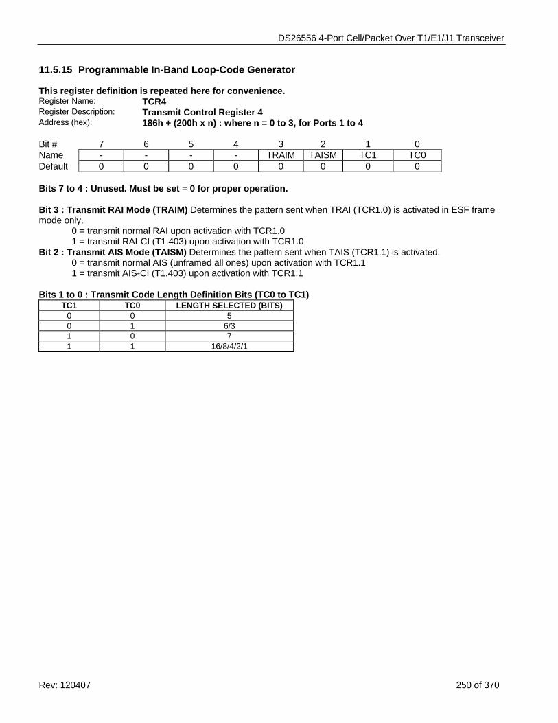
DS26556 4-Port Cell/Packet Over T1/E1/J1 Transceiver
Rev: 120407 250 of 370
11.5.15 Programmable In-Band Loop-Code Generator
This register definition is repeated here for convenience. Register Name: TCR4 Register Description: Transmit Control Register 4 Address (hex): 186h + (200h x n) : where n = 0 to 3, for Ports 1 to 4 Bit # 7 6 5 4 3 2 1 0 Name - - - - TRAIM TAISM TC1 TC0 Default 0 0 0 0 0 0 0 0 Bits 7 to 4 : Unused. Must be set = 0 for proper operation. Bit 3 : Transmit RAI Mode (TRAIM) Determines the pattern sent when TRAI (TCR1.0) is activated in ESF frame mode only. 0 = transmit normal RAI upon activation with TCR1.0 1 = transmit RAI-CI (T1.403) upon activation with TCR1.0 Bit 2 : Transmit AIS Mode (TAISM) Determines the pattern sent when TAIS (TCR1.1) is activated. 0 = transmit normal AIS (unframed all ones) upon activation with TCR1.1 1 = transmit AIS-CI (T1.403) upon activation with TCR1.1 Bits 1 to 0 : Transmit Code Length Definition Bits (TC0 to TC1)
TC1 TC0 LENGTH SELECTED (BITS) 0 0 5 0 1 6/3 1 0 7 1 1 16/8/4/2/1
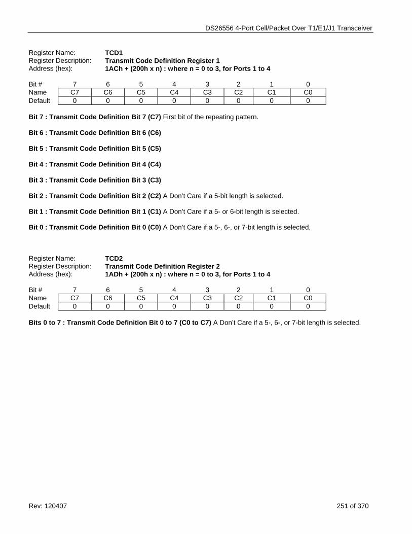
DS26556 4-Port Cell/Packet Over T1/E1/J1 Transceiver
Rev: 120407 251 of 370
Register Name: TCD1 Register Description: Transmit Code Definition Register 1 Address (hex): 1ACh + (200h x n) : where n = 0 to 3, for Ports 1 to 4 Bit # 7 6 5 4 3 2 1 0 Name C7 C6 C5 C4 C3 C2 C1 C0 Default 0 0 0 0 0 0 0 0 Bit 7 : Transmit Code Definition Bit 7 (C7) First bit of the repeating pattern. Bit 6 : Transmit Code Definition Bit 6 (C6) Bit 5 : Transmit Code Definition Bit 5 (C5) Bit 4 : Transmit Code Definition Bit 4 (C4) Bit 3 : Transmit Code Definition Bit 3 (C3) Bit 2 : Transmit Code Definition Bit 2 (C2) A Don’t Care if a 5-bit length is selected. Bit 1 : Transmit Code Definition Bit 1 (C1) A Don’t Care if a 5- or 6-bit length is selected. Bit 0 : Transmit Code Definition Bit 0 (C0) A Don’t Care if a 5-, 6-, or 7-bit length is selected. Register Name: TCD2 Register Description: Transmit Code Definition Register 2 Address (hex): 1ADh + (200h x n) : where n = 0 to 3, for Ports 1 to 4 Bit # 7 6 5 4 3 2 1 0 Name C7 C6 C5 C4 C3 C2 C1 C0 Default 0 0 0 0 0 0 0 0 Bits 0 to 7 : Transmit Code Definition Bit 0 to 7 (C0 to C7) A Don’t Care if a 5-, 6-, or 7-bit length is selected.
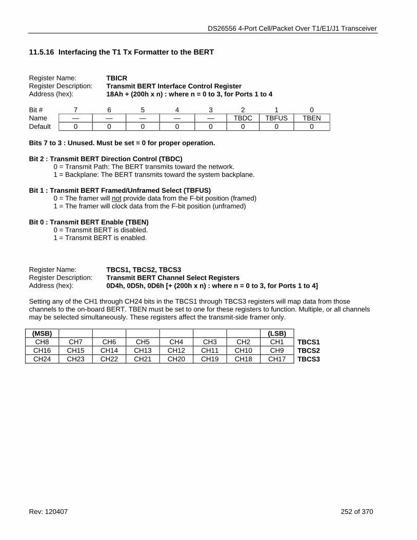
DS26556 4-Port Cell/Packet Over T1/E1/J1 Transceiver
Rev: 120407 252 of 370
11.5.16 Interfacing the T1 Tx Formatter to the BERT Register Name: TBICR Register Description: Transmit BERT Interface Control Register Address (hex): 18Ah + (200h x n) : where n = 0 to 3, for Ports 1 to 4 Bit # 7 6 5 4 3 2 1 0 Name — — — — — TBDC TBFUS TBEN Default 0 0 0 0 0 0 0 0 Bits 7 to 3 : Unused. Must be set = 0 for proper operation. Bit 2 : Transmit BERT Direction Control (TBDC) 0 = Transmit Path: The BERT transmits toward the network.
1 = Backplane: The BERT transmits toward the system backplane. Bit 1 : Transmit BERT Framed/Unframed Select (TBFUS)
0 = The framer will not provide data from the F-bit position (framed) 1 = The framer will clock data from the F-bit position (unframed)
Bit 0 : Transmit BERT Enable (TBEN) 0 = Transmit BERT is disabled.
1 = Transmit BERT is enabled. Register Name: TBCS1, TBCS2, TBCS3 Register Description: Transmit BERT Channel Select Registers Address (hex): 0D4h, 0D5h, 0D6h [+ (200h x n) : where n = 0 to 3, for Ports 1 to 4] Setting any of the CH1 through CH24 bits in the TBCS1 through TBCS3 registers will map data from those channels to the on-board BERT. TBEN must be set to one for these registers to function. Multiple, or all channels may be selected simultaneously. These registers affect the transmit-side framer only. (MSB) (LSB) CH8 CH7 CH6 CH5 CH4 CH3 CH2 CH1 TBCS1 CH16 CH15 CH14 CH13 CH12 CH11 CH10 CH9 TBCS2 CH24 CH23 CH22 CH21 CH20 CH19 CH18 CH17 TBCS3
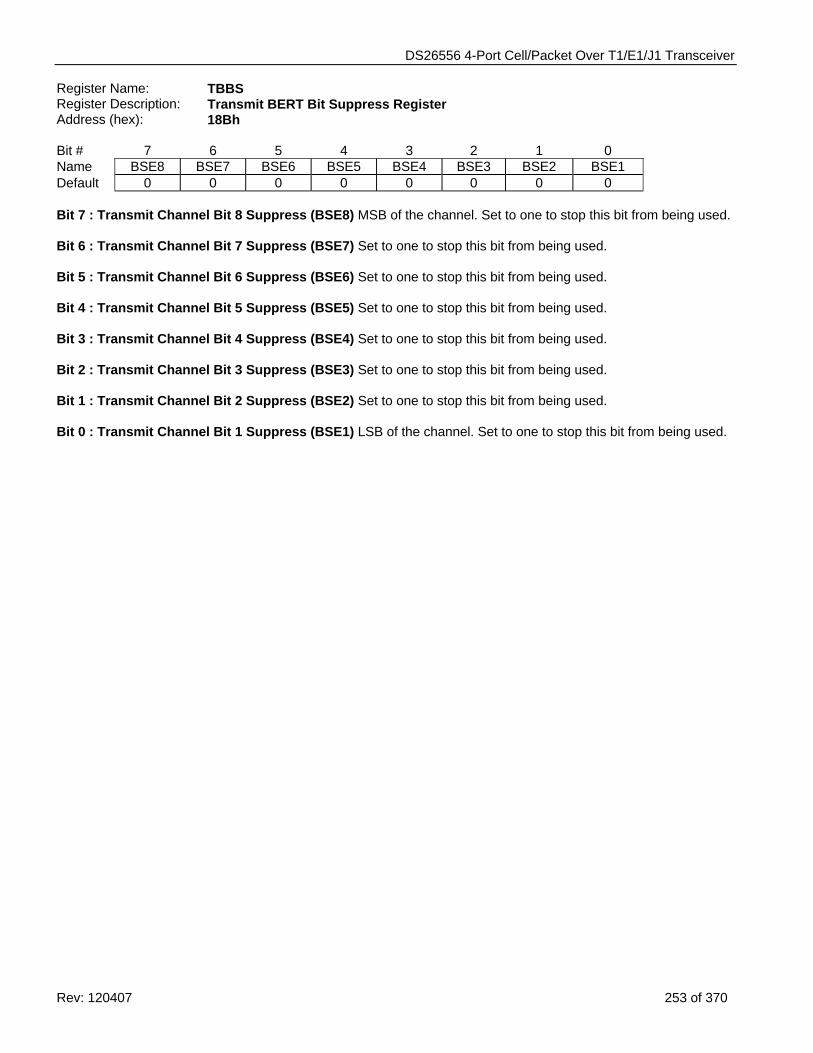
DS26556 4-Port Cell/Packet Over T1/E1/J1 Transceiver
Rev: 120407 253 of 370
Register Name: TBBS Register Description: Transmit BERT Bit Suppress Register Address (hex): 18Bh Bit # 7 6 5 4 3 2 1 0 Name BSE8 BSE7 BSE6 BSE5 BSE4 BSE3 BSE2 BSE1 Default 0 0 0 0 0 0 0 0 Bit 7 : Transmit Channel Bit 8 Suppress (BSE8) MSB of the channel. Set to one to stop this bit from being used. Bit 6 : Transmit Channel Bit 7 Suppress (BSE7) Set to one to stop this bit from being used. Bit 5 : Transmit Channel Bit 6 Suppress (BSE6) Set to one to stop this bit from being used. Bit 4 : Transmit Channel Bit 5 Suppress (BSE5) Set to one to stop this bit from being used. Bit 3 : Transmit Channel Bit 4 Suppress (BSE4) Set to one to stop this bit from being used. Bit 2 : Transmit Channel Bit 3 Suppress (BSE3) Set to one to stop this bit from being used. Bit 1 : Transmit Channel Bit 2 Suppress (BSE2) Set to one to stop this bit from being used. Bit 0 : Transmit Channel Bit 1 Suppress (BSE1) LSB of the channel. Set to one to stop this bit from being used.
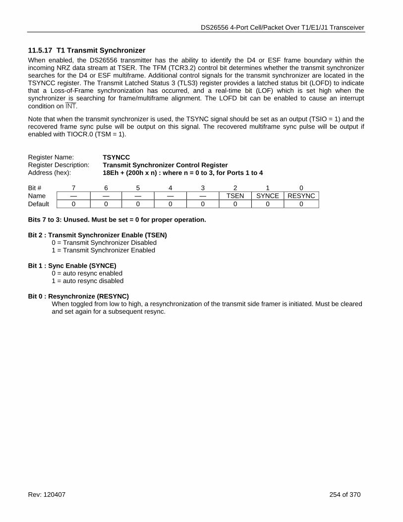
DS26556 4-Port Cell/Packet Over T1/E1/J1 Transceiver
Rev: 120407 254 of 370
11.5.17 T1 Transmit Synchronizer When enabled, the DS26556 transmitter has the ability to identify the D4 or ESF frame boundary within the incoming NRZ data stream at TSER. The TFM (TCR3.2) control bit determines whether the transmit synchronizer searches for the D4 or ESF multiframe. Additional control signals for the transmit synchronizer are located in the TSYNCC register. The Transmit Latched Status 3 (TLS3) register provides a latched status bit (LOFD) to indicate that a Loss-of-Frame synchronization has occurred, and a real-time bit (LOF) which is set high when the synchronizer is searching for frame/multiframe alignment. The LOFD bit can be enabled to cause an interrupt condition on INT.
Note that when the transmit synchronizer is used, the TSYNC signal should be set as an output (TSIO = 1) and the recovered frame sync pulse will be output on this signal. The recovered multiframe sync pulse will be output if enabled with TIOCR.0 (TSM = 1). Register Name: TSYNCC Register Description: Transmit Synchronizer Control Register Address (hex): 18Eh + (200h x n) : where n = 0 to 3, for Ports 1 to 4 Bit # 7 6 5 4 3 2 1 0 Name — — — — — TSEN SYNCE RESYNC Default 0 0 0 0 0 0 0 0 Bits 7 to 3: Unused. Must be set = 0 for proper operation. Bit 2 : Transmit Synchronizer Enable (TSEN)
0 = Transmit Synchronizer Disabled 1 = Transmit Synchronizer Enabled
Bit 1 : Sync Enable (SYNCE) 0 = auto resync enabled 1 = auto resync disabled
Bit 0 : Resynchronize (RESYNC)
When toggled from low to high, a resynchronization of the transmit side framer is initiated. Must be cleared and set again for a subsequent resync.
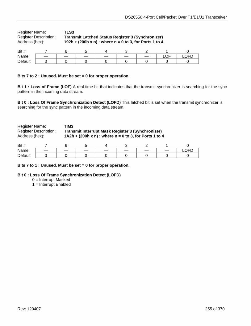
DS26556 4-Port Cell/Packet Over T1/E1/J1 Transceiver
Rev: 120407 255 of 370
Register Name: TLS3 Register Description: Transmit Latched Status Register 3 (Synchronizer) Address (hex): 192h + (200h x n) : where n = 0 to 3, for Ports 1 to 4 Bit # 7 6 5 4 3 2 1 0 Name — — — — — — LOF LOFD Default 0 0 0 0 0 0 0 0 Bits 7 to 2 : Unused. Must be set = 0 for proper operation. Bit 1 : Loss of Frame (LOF) A real-time bit that indicates that the transmit synchronizer is searching for the sync pattern in the incoming data stream. Bit 0 : Loss Of Frame Synchronization Detect (LOFD) This latched bit is set when the transmit synchronizer is searching for the sync pattern in the incoming data stream. Register Name: TIM3 Register Description: Transmit Interrupt Mask Register 3 (Synchronizer) Address (hex): 1A2h + (200h x n) : where n = 0 to 3, for Ports 1 to 4 Bit # 7 6 5 4 3 2 1 0 Name — — — — — — — LOFD Default 0 0 0 0 0 0 0 0 Bits 7 to 1 : Unused. Must be set = 0 for proper operation. Bit 0 : Loss Of Frame Synchronization Detect (LOFD) 0 = Interrupt Masked
1 = Interrupt Enabled
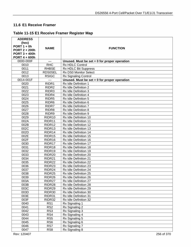
DS26556 4-Port Cell/Packet Over T1/E1/J1 Transceiver
Rev: 120407 256 of 370
11.6 E1 Receive Framer
Table 11-15 E1 Receive Framer Register Map ADDRESS
(hex) PORT 1 + 0h PORT 2 + 200h PORT 3 + 400h PORT 4 + 600h
NAME FUNCTION
0000-000F — Unused. Must be set = 0 for proper operation 0010 RHC Rx HDLC Control 0011 RHBSE Rx HDLC Bit Suppress 0012 RDS0SEL Rx DS0 Monitor Select 0013 RSIGC Rx Signaling Control
0014-001F — Unused. Must be set = 0 for proper operation 0020 RIDR1 Rx Idle Definition 1 0021 RIDR2 Rx Idle Definition 2 0022 RIDR3 Rx Idle Definition 3 0023 RIDR4 Rx Idle Definition 4 0024 RIDR5 Rx Idle Definition 5 0025 RIDR6 Rx Idle Definition 6 0026 RIDR7 Rx Idle Definition 7 0027 RIDR8 Rx Idle Definition 8 0028 RIDR9 Rx Idle Definition 9 0029 RIDR10 Rx Idle Definition 10 002A RIDR11 Rx Idle Definition 11 002B RIDR12 Rx Idle Definition 12 002C RIDR13 Rx Idle Definition 13 002D RIDR14 Rx Idle Definition 14 002E RIDR15 Rx Idle Definition 15 002F RIDR16 Rx Idle Definition 16 0030 RIDR17 Rx Idle Definition 17 0031 RIDR18 Rx Idle Definition 18 0032 RIDR19 Rx Idle Definition 19 0033 RIDR20 Rx Idle Definition 20 0034 RIDR21 Rx Idle Definition 21 0035 RIDR22 Rx Idle Definition 22 0036 RIDR23 Rx Idle Definition 23 0037 RIDR24 Rx Idle Definition 24 0038 RIDR25 Rx Idle Definition 25 0039 RIDR26 Rx Idle Definition 26 003A RIDR27 Rx Idle Definition 27 003B RIDR28 Rx Idle Definition 28 003C RIDR29 Rx Idle Definition 29 003D RIDR30 Rx Idle Definition 30 003E RIDR31 Rx Idle Definition 31 003F RIDR32 Rx Idle Definition 32 0040 RS1 Rx Signaling 1 0041 RS2 Rx Signaling 2 0042 RS3 Rx Signaling 3 0043 RS4 Rx Signaling 4 0044 RS5 Rx Signaling 5 0045 RS6 Rx Signaling 6 0046 RS7 Rx Signaling 7 0047 RS8 Rx Signaling 8
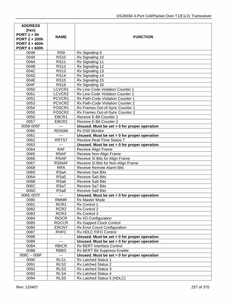
DS26556 4-Port Cell/Packet Over T1/E1/J1 Transceiver
Rev: 120407 257 of 370
ADDRESS (hex)
PORT 1 + 0h PORT 2 + 200h PORT 3 + 400h PORT 4 + 600h
NAME FUNCTION
0048 RS9 Rx Signaling 9 0049 RS10 Rx Signaling 10 004A RS11 Rx Signaling 11 004B RS12 Rx Signaling 12 004C RS13 Rx Signaling 13 004D RS14 Rx Signaling 14 004E RS15 Rx Signaling 15 004F RS16 Rx Signaling 16 0050 LCVCR1 Rx Line-Code Violation Counter 1 0051 LCVCR2 Rx Line-Code Violation Counter 2 0052 PCVCR1 Rx Path-Code Violation Counter 1 0053 PCVCR2 Rx Path-Code Violation Counter 2 0054 FOSCR1 Rx Frames Out-of-Sync Counter 1 0055 FOSCR2 Rx Frames Out-of-Sync Counter 2 0056 EBCR1 Receive E-Bit Counter 1 0057 EBCR2 Receive E-Bit Counter 2
0058-005F — Unused. Must be set = 0 for proper operation 0060 RDS0M Rx DS0 Monitor 0061 — Unused. Must be set = 0 for proper operation 0062 RRTS7 Receive Real-Time Status 7 0063 — Unused. Must be set = 0 for proper operation 0064 RAF Receive Align Frame 0065 RNAF Receive Non-Align Frame 0066 RSiAF Receive Si Bits for Align Frame 0067 RSiNAF Receive Si Bits for Non-Align Frame 0068 RRA Receive Remote Alarm Bits 0069 RSa4 Receive Sa4 Bits 006A RSa5 Receive Sa5 Bits 006B RSa6 Receive Sa6 Bits 006C RSa7 Receive Sa7 Bits 006D RSa8 Receive Sa8 Bits
006E-007F — Unused. Must be set = 0 for proper operation 0080 RMMR Rx Master Mode 0081 RCR1 Rx Control 1 0082 RCR2 Rx Control 2 0083 RCR3 Rx Control 3 0084 RIOCR Rx I/O Configuration 0085 RGCCR Rx Gapped Clock Control 0086 ERCNT Rx Error Count Configuration 0087 RHFC Rx HDLC FIFO Control 0088 - Unused. Must be set = 0 for proper operation 0089 — Unused. Must be set = 0 for proper operation 008A RBICR Rx BERT Interface Control 008B RBBS Rx BERT Bit Suppress Enable
008C – 008F — Unused. Must be set = 0 for proper operation 0090 RLS1 Rx Latched Status 1 0091 RLS2 Rx Latched Status 2 0092 RLS3 Rx Latched Status 3 0093 RLS4 Rx Latched Status 4 0094 RLS5 Rx Latched Status 5 (HDLC)
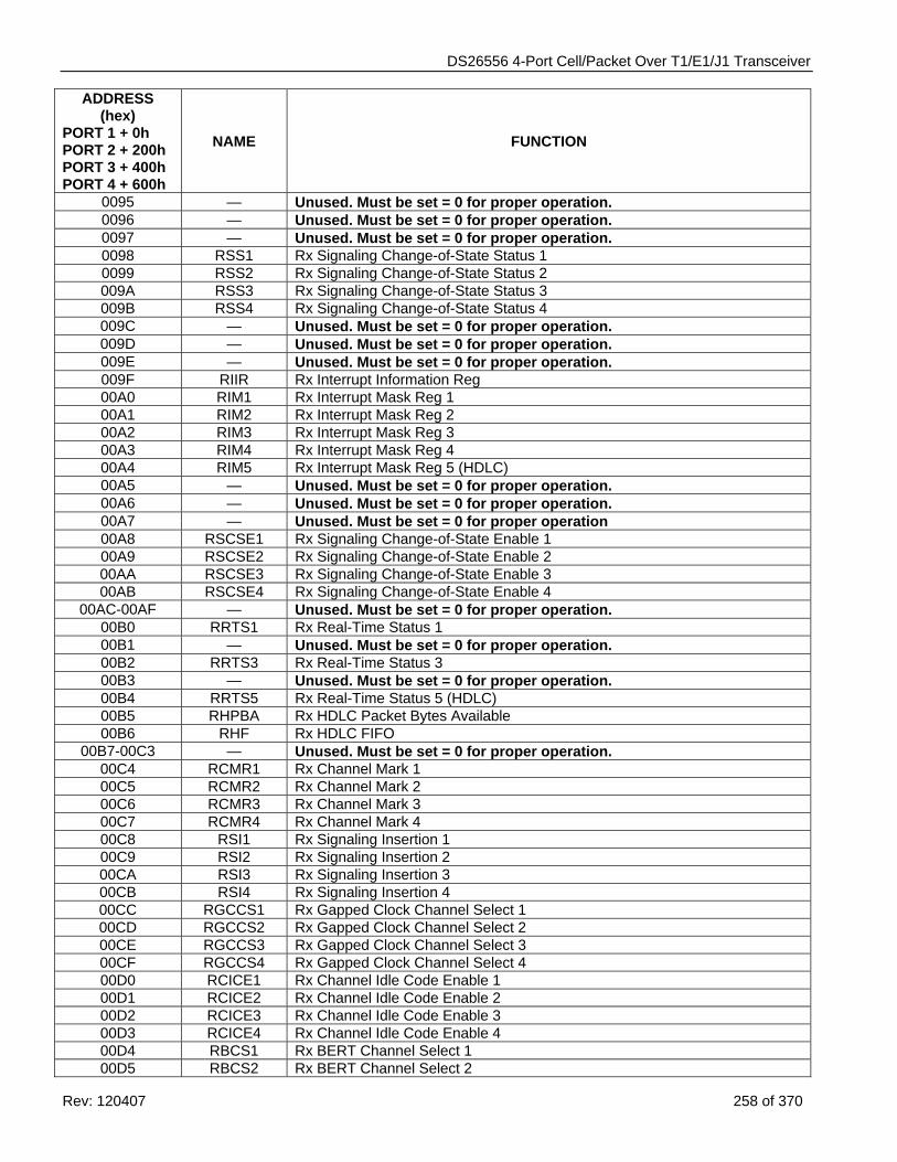
DS26556 4-Port Cell/Packet Over T1/E1/J1 Transceiver
Rev: 120407 258 of 370
ADDRESS (hex)
PORT 1 + 0h PORT 2 + 200h PORT 3 + 400h PORT 4 + 600h
NAME FUNCTION
0095 — Unused. Must be set = 0 for proper operation. 0096 — Unused. Must be set = 0 for proper operation. 0097 — Unused. Must be set = 0 for proper operation. 0098 RSS1 Rx Signaling Change-of-State Status 1 0099 RSS2 Rx Signaling Change-of-State Status 2 009A RSS3 Rx Signaling Change-of-State Status 3 009B RSS4 Rx Signaling Change-of-State Status 4 009C — Unused. Must be set = 0 for proper operation. 009D — Unused. Must be set = 0 for proper operation. 009E — Unused. Must be set = 0 for proper operation. 009F RIIR Rx Interrupt Information Reg 00A0 RIM1 Rx Interrupt Mask Reg 1 00A1 RIM2 Rx Interrupt Mask Reg 2 00A2 RIM3 Rx Interrupt Mask Reg 3 00A3 RIM4 Rx Interrupt Mask Reg 4 00A4 RIM5 Rx Interrupt Mask Reg 5 (HDLC) 00A5 — Unused. Must be set = 0 for proper operation. 00A6 — Unused. Must be set = 0 for proper operation. 00A7 — Unused. Must be set = 0 for proper operation 00A8 RSCSE1 Rx Signaling Change-of-State Enable 1 00A9 RSCSE2 Rx Signaling Change-of-State Enable 2 00AA RSCSE3 Rx Signaling Change-of-State Enable 3 00AB RSCSE4 Rx Signaling Change-of-State Enable 4
00AC-00AF — Unused. Must be set = 0 for proper operation. 00B0 RRTS1 Rx Real-Time Status 1 00B1 — Unused. Must be set = 0 for proper operation. 00B2 RRTS3 Rx Real-Time Status 3 00B3 — Unused. Must be set = 0 for proper operation. 00B4 RRTS5 Rx Real-Time Status 5 (HDLC) 00B5 RHPBA Rx HDLC Packet Bytes Available 00B6 RHF Rx HDLC FIFO
00B7-00C3 — Unused. Must be set = 0 for proper operation. 00C4 RCMR1 Rx Channel Mark 1 00C5 RCMR2 Rx Channel Mark 2 00C6 RCMR3 Rx Channel Mark 3 00C7 RCMR4 Rx Channel Mark 4 00C8 RSI1 Rx Signaling Insertion 1 00C9 RSI2 Rx Signaling Insertion 2 00CA RSI3 Rx Signaling Insertion 3 00CB RSI4 Rx Signaling Insertion 4 00CC RGCCS1 Rx Gapped Clock Channel Select 1 00CD RGCCS2 Rx Gapped Clock Channel Select 2 00CE RGCCS3 Rx Gapped Clock Channel Select 3 00CF RGCCS4 Rx Gapped Clock Channel Select 4 00D0 RCICE1 Rx Channel Idle Code Enable 1 00D1 RCICE2 Rx Channel Idle Code Enable 2 00D2 RCICE3 Rx Channel Idle Code Enable 3 00D3 RCICE4 Rx Channel Idle Code Enable 4 00D4 RBCS1 Rx BERT Channel Select 1 00D5 RBCS2 Rx BERT Channel Select 2
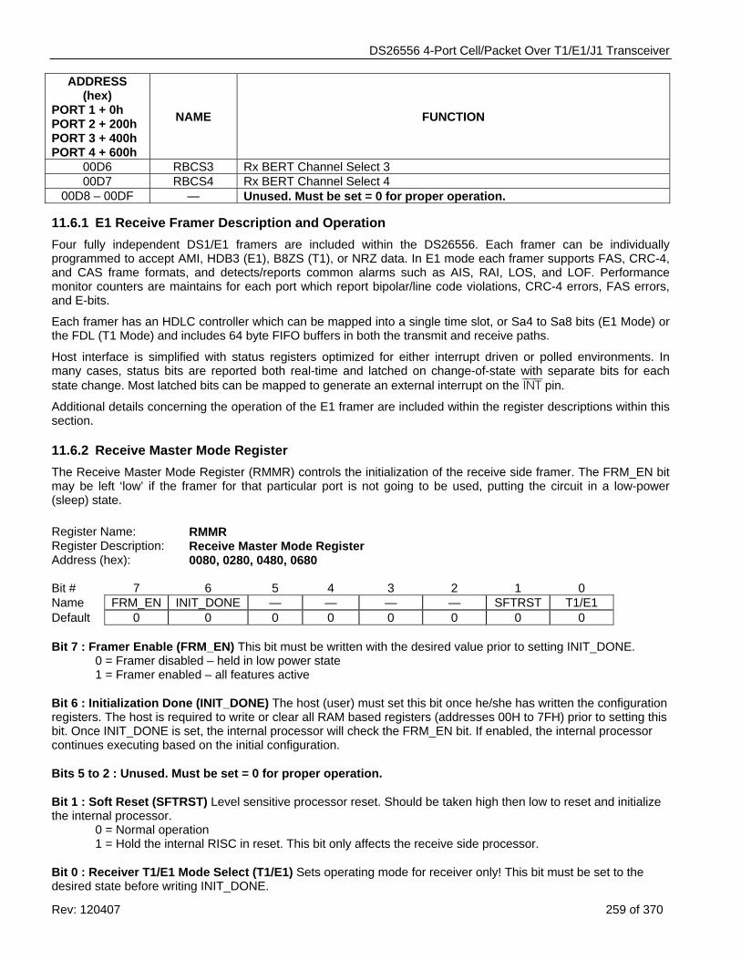
DS26556 4-Port Cell/Packet Over T1/E1/J1 Transceiver
Rev: 120407 259 of 370
ADDRESS (hex)
PORT 1 + 0h PORT 2 + 200h PORT 3 + 400h PORT 4 + 600h
NAME FUNCTION
00D6 RBCS3 Rx BERT Channel Select 3 00D7 RBCS4 Rx BERT Channel Select 4
00D8 – 00DF — Unused. Must be set = 0 for proper operation.
11.6.1 E1 Receive Framer Description and Operation Four fully independent DS1/E1 framers are included within the DS26556. Each framer can be individually programmed to accept AMI, HDB3 (E1), B8ZS (T1), or NRZ data. In E1 mode each framer supports FAS, CRC-4, and CAS frame formats, and detects/reports common alarms such as AIS, RAI, LOS, and LOF. Performance monitor counters are maintains for each port which report bipolar/line code violations, CRC-4 errors, FAS errors, and E-bits.
Each framer has an HDLC controller which can be mapped into a single time slot, or Sa4 to Sa8 bits (E1 Mode) or the FDL (T1 Mode) and includes 64 byte FIFO buffers in both the transmit and receive paths.
Host interface is simplified with status registers optimized for either interrupt driven or polled environments. In many cases, status bits are reported both real-time and latched on change-of-state with separate bits for each state change. Most latched bits can be mapped to generate an external interrupt on the INT pin.
Additional details concerning the operation of the E1 framer are included within the register descriptions within this section.
11.6.2 Receive Master Mode Register The Receive Master Mode Register (RMMR) controls the initialization of the receive side framer. The FRM_EN bit may be left ‘low’ if the framer for that particular port is not going to be used, putting the circuit in a low-power (sleep) state. Register Name: RMMR Register Description: Receive Master Mode Register Address (hex): 0080, 0280, 0480, 0680 Bit # 7 6 5 4 3 2 1 0 Name FRM_EN INIT_DONE — — — — SFTRST T1/E1 Default 0 0 0 0 0 0 0 0 Bit 7 : Framer Enable (FRM_EN) This bit must be written with the desired value prior to setting INIT_DONE. 0 = Framer disabled – held in low power state 1 = Framer enabled – all features active Bit 6 : Initialization Done (INIT_DONE) The host (user) must set this bit once he/she has written the configuration registers. The host is required to write or clear all RAM based registers (addresses 00H to 7FH) prior to setting this bit. Once INIT_DONE is set, the internal processor will check the FRM_EN bit. If enabled, the internal processor continues executing based on the initial configuration. Bits 5 to 2 : Unused. Must be set = 0 for proper operation. Bit 1 : Soft Reset (SFTRST) Level sensitive processor reset. Should be taken high then low to reset and initialize the internal processor.
0 = Normal operation 1 = Hold the internal RISC in reset. This bit only affects the receive side processor.
Bit 0 : Receiver T1/E1 Mode Select (T1/E1) Sets operating mode for receiver only! This bit must be set to the desired state before writing INIT_DONE.

DS26556 4-Port Cell/Packet Over T1/E1/J1 Transceiver
Rev: 120407 260 of 370
0 = T1 operation 1 = E1 operation
DS26556 4-Port Cell/Packet Over T1/E1/J1 Transceiver
Rev: 120407 261 of 370
11.6.3 Interrupt Information Registers The Interrupt Information Registers provide an indication of which DS26556 Status Registers are generating an interrupt. When an interrupt occurs, the host can read RIIR to quickly identify which of the 6 E1 receive status registers are causing the interrupt. The Interrupt Information Register bits will clear once the appropriate interrupt has been serviced and cleared, as long as no other interrupt condition is present in the associated status register. Status bits that have been masked via the Receive Interrupt Mask (RIMx) registers, will also be masked from the IIR registers.
Register Name: RIIR Register Description: Receive Interrupt Information Register Address (hex): 009F, 029F, 049F, 069F Bit # 7 6 5 4 3 2 1 0 Name RLS6 RLS5 RLS4 RLS3 RLS2 RLS1 Default 0 0 0 0 0 0 0 0
11.6.4 E1 Receive Control Registers
Register Name: RCR1 Register Description: Receive Control Register 1 Address (hex): 0081, 0281, 0481, 0681 Bit # 7 6 5 4 3 2 1 0 Name — RHDB3 RSIGM RG802 RCRC4 FRC SYNCE RESYNC Default 0 0 0 0 0 0 0 0
Bit 7 : Unused. Must be set = 0 for proper operation. Bit 6 : Receive HDB3 Enable (RHDB3)
0 = HDB3 disabled 1 = HDB3 enabled
Bit 5 : Receive Signaling Mode Select (RSIGM)
0 = CAS signaling mode 1 = CCS signaling mode
Bit 4 : Receive G.802 Enable (RG802)
0 = do not force RCHMRK high during bit 1 of time slot 26 1 = force RCHMRK high during bit 1 of time slot 26
Bit 3 : Receive CRC4 Enable (RCRC4)
0 = CRC4 disabled 1 = CRC4 enabled
Bit 2 : Frame Resync Criteria (FRC)
0 = resync if FAS received in error 3 consecutive times 1 = resync if FAS or bit 2 of non-FAS is received in error 3 consecutive times
Bit 1 : Sync Enable (SYNCE)
0 = auto resync enabled 1 = auto resync disabled
Bit 0 : Resynchronize (RESYNC)
When toggled from low to high, a resynchronization of the receive-side framer is initiated. Must be cleared and set again for a subsequent resync.
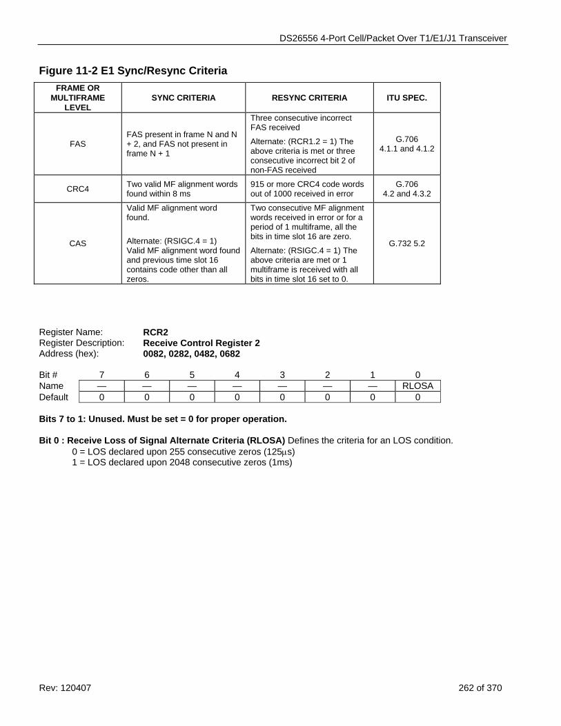
DS26556 4-Port Cell/Packet Over T1/E1/J1 Transceiver
Rev: 120407 262 of 370
Figure 11-2 E1 Sync/Resync Criteria FRAME OR
MULTIFRAME LEVEL
SYNC CRITERIA RESYNC CRITERIA ITU SPEC.
FAS FAS present in frame N and N + 2, and FAS not present in frame N + 1
Three consecutive incorrect FAS received
Alternate: (RCR1.2 = 1) The above criteria is met or three consecutive incorrect bit 2 of non-FAS received
G.706 4.1.1 and 4.1.2
CRC4 Two valid MF alignment words found within 8 ms
915 or more CRC4 code words out of 1000 received in error
G.706 4.2 and 4.3.2
CAS
Valid MF alignment word found.
Alternate: (RSIGC.4 = 1) Valid MF alignment word found and previous time slot 16 contains code other than all zeros.
Two consecutive MF alignment words received in error or for a period of 1 multiframe, all the bits in time slot 16 are zero.
Alternate: (RSIGC.4 = 1) The above criteria are met or 1 multiframe is received with all bits in time slot 16 set to 0.
G.732 5.2
Register Name: RCR2 Register Description: Receive Control Register 2 Address (hex): 0082, 0282, 0482, 0682 Bit # 7 6 5 4 3 2 1 0 Name — — — — — — — RLOSA Default 0 0 0 0 0 0 0 0 Bits 7 to 1: Unused. Must be set = 0 for proper operation. Bit 0 : Receive Loss of Signal Alternate Criteria (RLOSA) Defines the criteria for an LOS condition.
0 = LOS declared upon 255 consecutive zeros (125μs) 1 = LOS declared upon 2048 consecutive zeros (1ms)
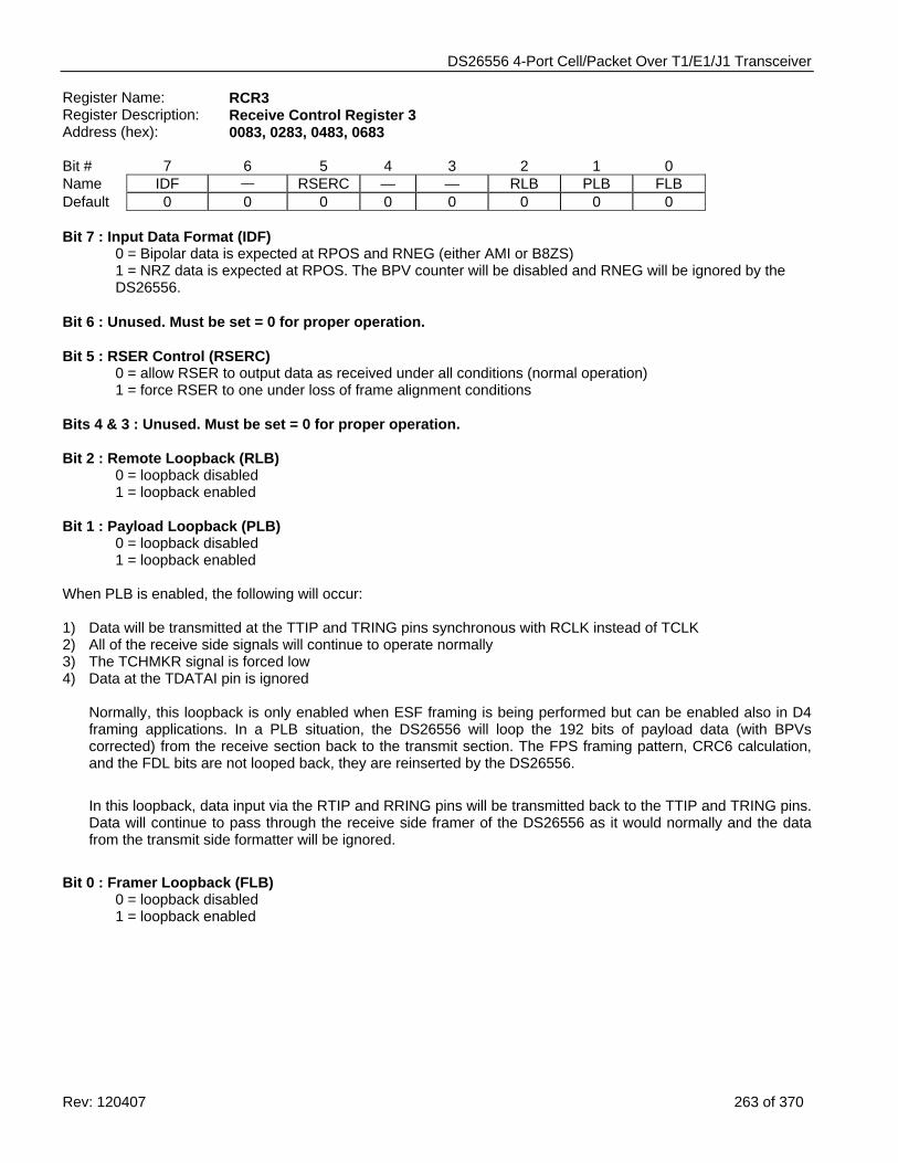
DS26556 4-Port Cell/Packet Over T1/E1/J1 Transceiver
Rev: 120407 263 of 370
Register Name: RCR3 Register Description: Receive Control Register 3 Address (hex): 0083, 0283, 0483, 0683 Bit # 7 6 5 4 3 2 1 0 Name IDF — RSERC — — RLB PLB FLB Default 0 0 0 0 0 0 0 0 Bit 7 : Input Data Format (IDF) 0 = Bipolar data is expected at RPOS and RNEG (either AMI or B8ZS)
1 = NRZ data is expected at RPOS. The BPV counter will be disabled and RNEG will be ignored by the DS26556.
Bit 6 : Unused. Must be set = 0 for proper operation. Bit 5 : RSER Control (RSERC)
0 = allow RSER to output data as received under all conditions (normal operation) 1 = force RSER to one under loss of frame alignment conditions
Bits 4 & 3 : Unused. Must be set = 0 for proper operation. Bit 2 : Remote Loopback (RLB)
0 = loopback disabled 1 = loopback enabled
Bit 1 : Payload Loopback (PLB)
0 = loopback disabled 1 = loopback enabled
When PLB is enabled, the following will occur: 1) Data will be transmitted at the TTIP and TRING pins synchronous with RCLK instead of TCLK 2) All of the receive side signals will continue to operate normally 3) The TCHMKR signal is forced low 4) Data at the TDATAI pin is ignored
Normally, this loopback is only enabled when ESF framing is being performed but can be enabled also in D4 framing applications. In a PLB situation, the DS26556 will loop the 192 bits of payload data (with BPVs corrected) from the receive section back to the transmit section. The FPS framing pattern, CRC6 calculation, and the FDL bits are not looped back, they are reinserted by the DS26556.
In this loopback, data input via the RTIP and RRING pins will be transmitted back to the TTIP and TRING pins. Data will continue to pass through the receive side framer of the DS26556 as it would normally and the data from the transmit side formatter will be ignored.
Bit 0 : Framer Loopback (FLB)
0 = loopback disabled 1 = loopback enabled
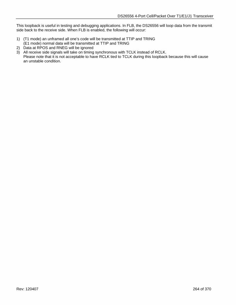
DS26556 4-Port Cell/Packet Over T1/E1/J1 Transceiver
Rev: 120407 264 of 370
This loopback is useful in testing and debugging applications. In FLB, the DS26556 will loop data from the transmit side back to the receive side. When FLB is enabled, the following will occur: 1) (T1 mode) an unframed all one’s code will be transmitted at TTIP and TRING
(E1 mode) normal data will be transmitted at TTIP and TRING 2) Data at RPOS and RNEG will be ignored 3) All receive side signals will take on timing synchronous with TCLK instead of RCLK.
Please note that it is not acceptable to have RCLK tied to TCLK during this loopback because this will cause an unstable condition.
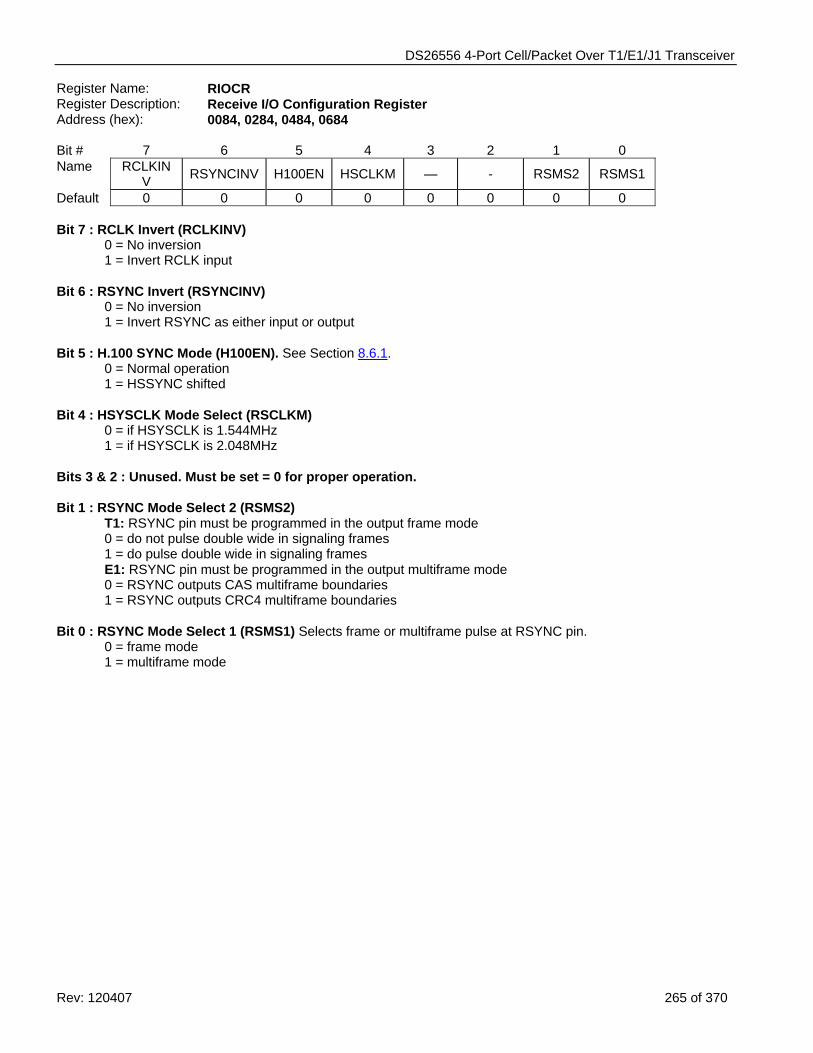
DS26556 4-Port Cell/Packet Over T1/E1/J1 Transceiver
Rev: 120407 265 of 370
Register Name: RIOCR Register Description: Receive I/O Configuration Register Address (hex): 0084, 0284, 0484, 0684 Bit # 7 6 5 4 3 2 1 0 Name RCLKIN
V RSYNCINV H100EN HSCLKM — - RSMS2 RSMS1
Default 0 0 0 0 0 0 0 0 Bit 7 : RCLK Invert (RCLKINV)
0 = No inversion 1 = Invert RCLK input
Bit 6 : RSYNC Invert (RSYNCINV)
0 = No inversion 1 = Invert RSYNC as either input or output
Bit 5 : H.100 SYNC Mode (H100EN). See Section 8.6.1.
0 = Normal operation 1 = HSSYNC shifted
Bit 4 : HSYSCLK Mode Select (RSCLKM)
0 = if HSYSCLK is 1.544MHz 1 = if HSYSCLK is 2.048MHz
Bits 3 & 2 : Unused. Must be set = 0 for proper operation. Bit 1 : RSYNC Mode Select 2 (RSMS2)
T1: RSYNC pin must be programmed in the output frame mode 0 = do not pulse double wide in signaling frames 1 = do pulse double wide in signaling frames E1: RSYNC pin must be programmed in the output multiframe mode 0 = RSYNC outputs CAS multiframe boundaries 1 = RSYNC outputs CRC4 multiframe boundaries
Bit 0 : RSYNC Mode Select 1 (RSMS1) Selects frame or multiframe pulse at RSYNC pin.
0 = frame mode 1 = multiframe mode
DS26556 4-Port Cell/Packet Over T1/E1/J1 Transceiver
Rev: 120407 266 of 370
11.6.5 E1 Receive Status and Information When a particular event has occurred (or is occurring), the appropriate bit in one of these registers will be set to a one. Status bits may operate in either a latched or real-time fashion. Some latched bits may be enabled to generate a hardware interrupt via the INT signal. Real-Time Bits Some status bits operate in a real-time fashion. These bits are read-only and indicate the present state of an alarm or a condition. Real-time bits remain stable and valid during the host read operation. The current value of the internal status signals can be read at any time from the real time status registers without changing any the latched status register bits Latched Bits When an event or an alarm occurs and a latched bit is set to a one, it will remain set until cleared by the user. These bits typically respond on a change-of-state for an alarm, condition, or event; and operate in a read-then-write fashion. The user should read the value of the desired status bit, and then write a 1 to that particular bit location in order to clear the latched value (write a 0 to locations not to be cleared). Once the bit is cleared, it will not be set again until the event has occurred again. Mask Bits Some of the alarms and events can be either masked or unmasked from the interrupt pin via the Interrupt Mask Registers (RIMx). When unmasked, the INT signal will be forced low when the enabled event or condition occurs. The INT pin will be allowed to return high (if no other unmasked interrupts are present) when the user reads then clears (with a write) the alarm bit that caused the interrupt to occur. Note that the latched status bit and the INT pin will clear even if the alarm is still present. Note that some conditions may have multiple status indications. For example, Receive Loss of Frame (RLOF) provides the following indications:
RRTS1.0 (RLOF)
Real-time indication that the receiver is not synchronized with incoming data stream. Read-only bit that remains high as long as the condition is present.
RLS1.0 (RLOFD)
Latched indication that the receiver has loss synchronization since the bit was last cleared. Bit will clear when written by the user, even if the condition is still present (rising edge detect of RRTS1.0).
RLS1.4 (RLOFC)
Latched indication that the receiver has reacquired synchronization since the bit was last cleared. Bit will clear when written by the user, even if the condition is still present (falling edge detect of RRTS1.0).
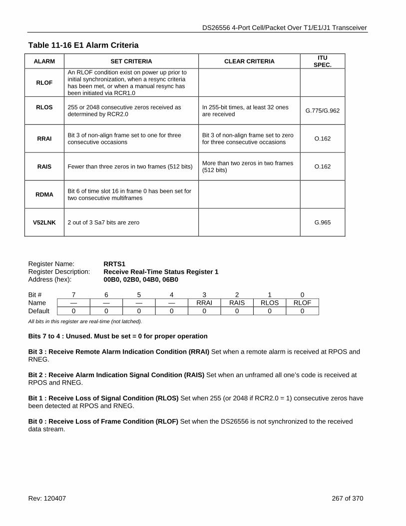
DS26556 4-Port Cell/Packet Over T1/E1/J1 Transceiver
Rev: 120407 267 of 370
Table 11-16 E1 Alarm Criteria
ALARM SET CRITERIA CLEAR CRITERIA ITU SPEC.
RLOF
An RLOF condition exist on power up prior to initial synchronization, when a resync criteria has been met, or when a manual resync has been initiated via RCR1.0
RLOS
255 or 2048 consecutive zeros received as determined by RCR2.0
In 255-bit times, at least 32 ones are received G.775/G.962
RRAI Bit 3 of non-align frame set to one for three consecutive occasions
Bit 3 of non-align frame set to zero for three consecutive occasions O.162
RAIS Fewer than three zeros in two frames (512 bits) More than two zeros in two frames (512 bits) O.162
RDMA Bit 6 of time slot 16 in frame 0 has been set for two consecutive multiframes
V52LNK 2 out of 3 Sa7 bits are zero G.965
Register Name: RRTS1 Register Description: Receive Real-Time Status Register 1 Address (hex): 00B0, 02B0, 04B0, 06B0 Bit # 7 6 5 4 3 2 1 0 Name — — — — RRAI RAIS RLOS RLOF Default 0 0 0 0 0 0 0 0 All bits in this register are real-time (not latched). Bits 7 to 4 : Unused. Must be set = 0 for proper operation Bit 3 : Receive Remote Alarm Indication Condition (RRAI) Set when a remote alarm is received at RPOS and RNEG. Bit 2 : Receive Alarm Indication Signal Condition (RAIS) Set when an unframed all one’s code is received at RPOS and RNEG. Bit 1 : Receive Loss of Signal Condition (RLOS) Set when 255 (or 2048 if RCR2.0 = 1) consecutive zeros have been detected at RPOS and RNEG. Bit 0 : Receive Loss of Frame Condition (RLOF) Set when the DS26556 is not synchronized to the received data stream.
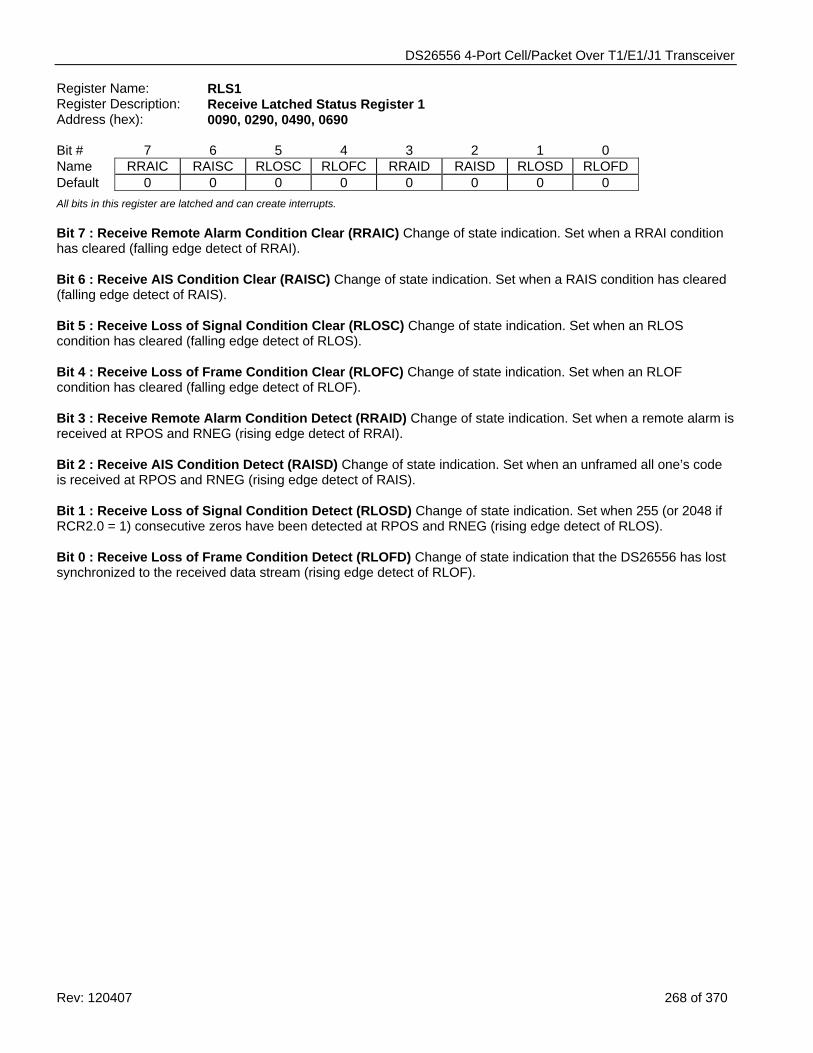
DS26556 4-Port Cell/Packet Over T1/E1/J1 Transceiver
Rev: 120407 268 of 370
Register Name: RLS1 Register Description: Receive Latched Status Register 1 Address (hex): 0090, 0290, 0490, 0690 Bit # 7 6 5 4 3 2 1 0 Name RRAIC RAISC RLOSC RLOFC RRAID RAISD RLOSD RLOFD Default 0 0 0 0 0 0 0 0 All bits in this register are latched and can create interrupts. Bit 7 : Receive Remote Alarm Condition Clear (RRAIC) Change of state indication. Set when a RRAI condition has cleared (falling edge detect of RRAI). Bit 6 : Receive AIS Condition Clear (RAISC) Change of state indication. Set when a RAIS condition has cleared (falling edge detect of RAIS). Bit 5 : Receive Loss of Signal Condition Clear (RLOSC) Change of state indication. Set when an RLOS condition has cleared (falling edge detect of RLOS). Bit 4 : Receive Loss of Frame Condition Clear (RLOFC) Change of state indication. Set when an RLOF condition has cleared (falling edge detect of RLOF). Bit 3 : Receive Remote Alarm Condition Detect (RRAID) Change of state indication. Set when a remote alarm is received at RPOS and RNEG (rising edge detect of RRAI). Bit 2 : Receive AIS Condition Detect (RAISD) Change of state indication. Set when an unframed all one’s code is received at RPOS and RNEG (rising edge detect of RAIS). Bit 1 : Receive Loss of Signal Condition Detect (RLOSD) Change of state indication. Set when 255 (or 2048 if RCR2.0 = 1) consecutive zeros have been detected at RPOS and RNEG (rising edge detect of RLOS). Bit 0 : Receive Loss of Frame Condition Detect (RLOFD) Change of state indication that the DS26556 has lost synchronized to the received data stream (rising edge detect of RLOF).
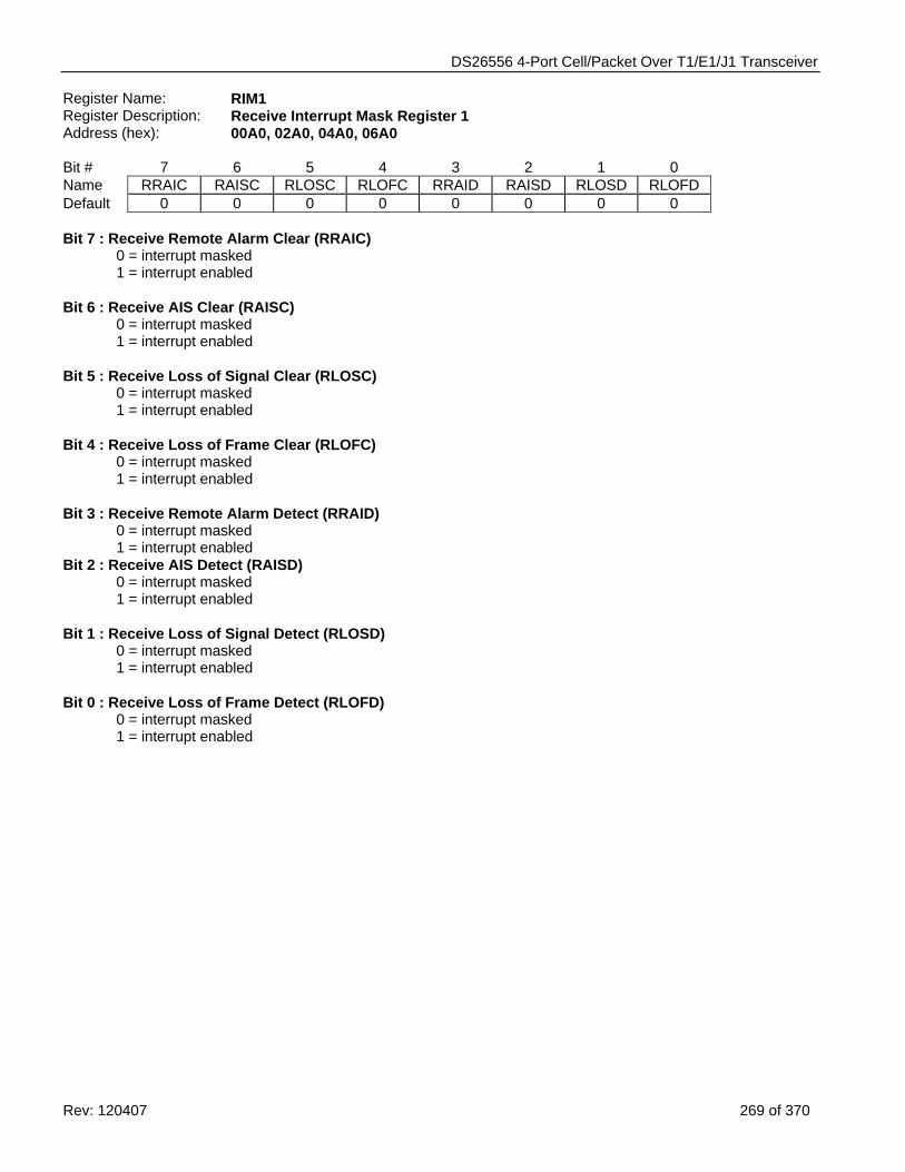
DS26556 4-Port Cell/Packet Over T1/E1/J1 Transceiver
Rev: 120407 269 of 370
Register Name: RIM1 Register Description: Receive Interrupt Mask Register 1 Address (hex): 00A0, 02A0, 04A0, 06A0 Bit # 7 6 5 4 3 2 1 0 Name RRAIC RAISC RLOSC RLOFC RRAID RAISD RLOSD RLOFD Default 0 0 0 0 0 0 0 0 Bit 7 : Receive Remote Alarm Clear (RRAIC)
0 = interrupt masked 1 = interrupt enabled
Bit 6 : Receive AIS Clear (RAISC)
0 = interrupt masked 1 = interrupt enabled
Bit 5 : Receive Loss of Signal Clear (RLOSC)
0 = interrupt masked 1 = interrupt enabled
Bit 4 : Receive Loss of Frame Clear (RLOFC)
0 = interrupt masked 1 = interrupt enabled
Bit 3 : Receive Remote Alarm Detect (RRAID)
0 = interrupt masked 1 = interrupt enabled
Bit 2 : Receive AIS Detect (RAISD) 0 = interrupt masked 1 = interrupt enabled
Bit 1 : Receive Loss of Signal Detect (RLOSD)
0 = interrupt masked 1 = interrupt enabled
Bit 0 : Receive Loss of Frame Detect (RLOFD)
0 = interrupt masked 1 = interrupt enabled
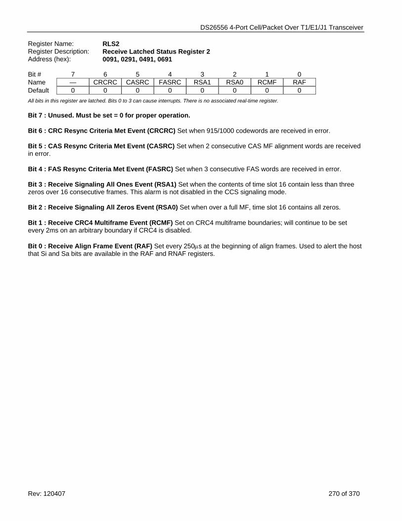
DS26556 4-Port Cell/Packet Over T1/E1/J1 Transceiver
Rev: 120407 270 of 370
Register Name: RLS2 Register Description: Receive Latched Status Register 2 Address (hex): 0091, 0291, 0491, 0691 Bit # 7 6 5 4 3 2 1 0 Name — CRCRC CASRC FASRC RSA1 RSA0 RCMF RAF Default 0 0 0 0 0 0 0 0 All bits in this register are latched. Bits 0 to 3 can cause interrupts. There is no associated real-time register. Bit 7 : Unused. Must be set = 0 for proper operation. Bit 6 : CRC Resync Criteria Met Event (CRCRC) Set when 915/1000 codewords are received in error. Bit 5 : CAS Resync Criteria Met Event (CASRC) Set when 2 consecutive CAS MF alignment words are received in error. Bit 4 : FAS Resync Criteria Met Event (FASRC) Set when 3 consecutive FAS words are received in error. Bit 3 : Receive Signaling All Ones Event (RSA1) Set when the contents of time slot 16 contain less than three zeros over 16 consecutive frames. This alarm is not disabled in the CCS signaling mode. Bit 2 : Receive Signaling All Zeros Event (RSA0) Set when over a full MF, time slot 16 contains all zeros. Bit 1 : Receive CRC4 Multiframe Event (RCMF) Set on CRC4 multiframe boundaries; will continue to be set every 2ms on an arbitrary boundary if CRC4 is disabled. Bit 0 : Receive Align Frame Event (RAF) Set every 250μs at the beginning of align frames. Used to alert the host that Si and Sa bits are available in the RAF and RNAF registers.
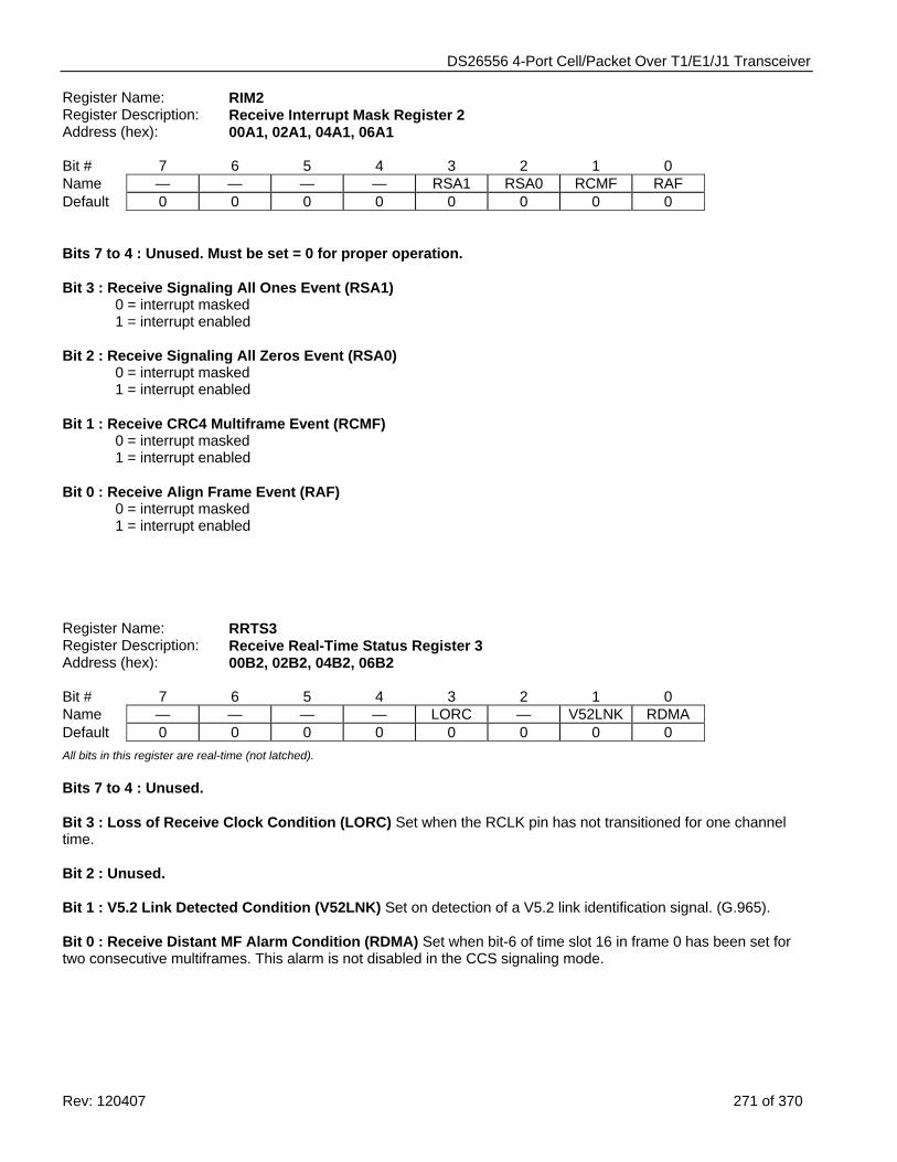
DS26556 4-Port Cell/Packet Over T1/E1/J1 Transceiver
Rev: 120407 271 of 370
Register Name: RIM2 Register Description: Receive Interrupt Mask Register 2 Address (hex): 00A1, 02A1, 04A1, 06A1 Bit # 7 6 5 4 3 2 1 0 Name — — — — RSA1 RSA0 RCMF RAF Default 0 0 0 0 0 0 0 0 Bits 7 to 4 : Unused. Must be set = 0 for proper operation. Bit 3 : Receive Signaling All Ones Event (RSA1)
0 = interrupt masked 1 = interrupt enabled
Bit 2 : Receive Signaling All Zeros Event (RSA0) 0 = interrupt masked 1 = interrupt enabled
Bit 1 : Receive CRC4 Multiframe Event (RCMF)
0 = interrupt masked 1 = interrupt enabled
Bit 0 : Receive Align Frame Event (RAF)
0 = interrupt masked 1 = interrupt enabled
Register Name: RRTS3 Register Description: Receive Real-Time Status Register 3 Address (hex): 00B2, 02B2, 04B2, 06B2 Bit # 7 6 5 4 3 2 1 0 Name — — — — LORC — V52LNK RDMA Default 0 0 0 0 0 0 0 0 All bits in this register are real-time (not latched). Bits 7 to 4 : Unused. Bit 3 : Loss of Receive Clock Condition (LORC) Set when the RCLK pin has not transitioned for one channel time. Bit 2 : Unused. Bit 1 : V5.2 Link Detected Condition (V52LNK) Set on detection of a V5.2 link identification signal. (G.965). Bit 0 : Receive Distant MF Alarm Condition (RDMA) Set when bit-6 of time slot 16 in frame 0 has been set for two consecutive multiframes. This alarm is not disabled in the CCS signaling mode.
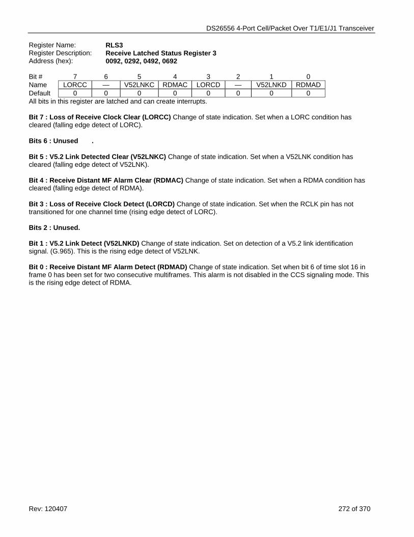
DS26556 4-Port Cell/Packet Over T1/E1/J1 Transceiver
Rev: 120407 272 of 370
Register Name: RLS3 Register Description: Receive Latched Status Register 3 Address (hex): 0092, 0292, 0492, 0692 Bit # 7 6 5 4 3 2 1 0 Name LORCC — V52LNKC RDMAC LORCD — V52LNKD RDMAD Default 0 0 0 0 0 0 0 0 All bits in this register are latched and can create interrupts. Bit 7 : Loss of Receive Clock Clear (LORCC) Change of state indication. Set when a LORC condition has cleared (falling edge detect of LORC). Bits 6 : Unused . Bit 5 : V5.2 Link Detected Clear (V52LNKC) Change of state indication. Set when a V52LNK condition has cleared (falling edge detect of V52LNK). Bit 4 : Receive Distant MF Alarm Clear (RDMAC) Change of state indication. Set when a RDMA condition has cleared (falling edge detect of RDMA). Bit 3 : Loss of Receive Clock Detect (LORCD) Change of state indication. Set when the RCLK pin has not transitioned for one channel time (rising edge detect of LORC). Bits 2 : Unused. Bit 1 : V5.2 Link Detect (V52LNKD) Change of state indication. Set on detection of a V5.2 link identification signal. (G.965). This is the rising edge detect of V52LNK. Bit 0 : Receive Distant MF Alarm Detect (RDMAD) Change of state indication. Set when bit 6 of time slot 16 in frame 0 has been set for two consecutive multiframes. This alarm is not disabled in the CCS signaling mode. This is the rising edge detect of RDMA.
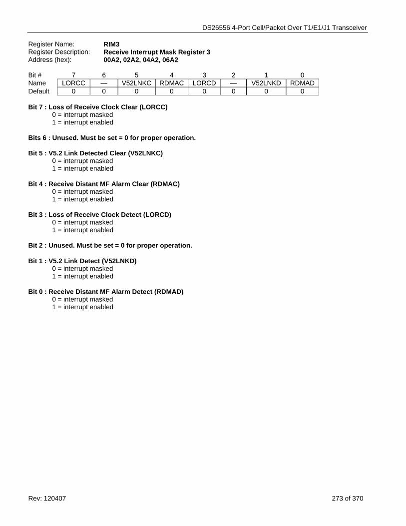
DS26556 4-Port Cell/Packet Over T1/E1/J1 Transceiver
Rev: 120407 273 of 370
Register Name: RIM3 Register Description: Receive Interrupt Mask Register 3 Address (hex): 00A2, 02A2, 04A2, 06A2 Bit # 7 6 5 4 3 2 1 0 Name LORCC — V52LNKC RDMAC LORCD — V52LNKD RDMAD Default 0 0 0 0 0 0 0 0 Bit 7 : Loss of Receive Clock Clear (LORCC)
0 = interrupt masked 1 = interrupt enabled
Bits 6 : Unused. Must be set = 0 for proper operation. Bit 5 : V5.2 Link Detected Clear (V52LNKC)
0 = interrupt masked 1 = interrupt enabled
Bit 4 : Receive Distant MF Alarm Clear (RDMAC)
0 = interrupt masked 1 = interrupt enabled
Bit 3 : Loss of Receive Clock Detect (LORCD)
0 = interrupt masked 1 = interrupt enabled
Bit 2 : Unused. Must be set = 0 for proper operation. Bit 1 : V5.2 Link Detect (V52LNKD)
0 = interrupt masked 1 = interrupt enabled
Bit 0 : Receive Distant MF Alarm Detect (RDMAD)
0 = interrupt masked 1 = interrupt enabled
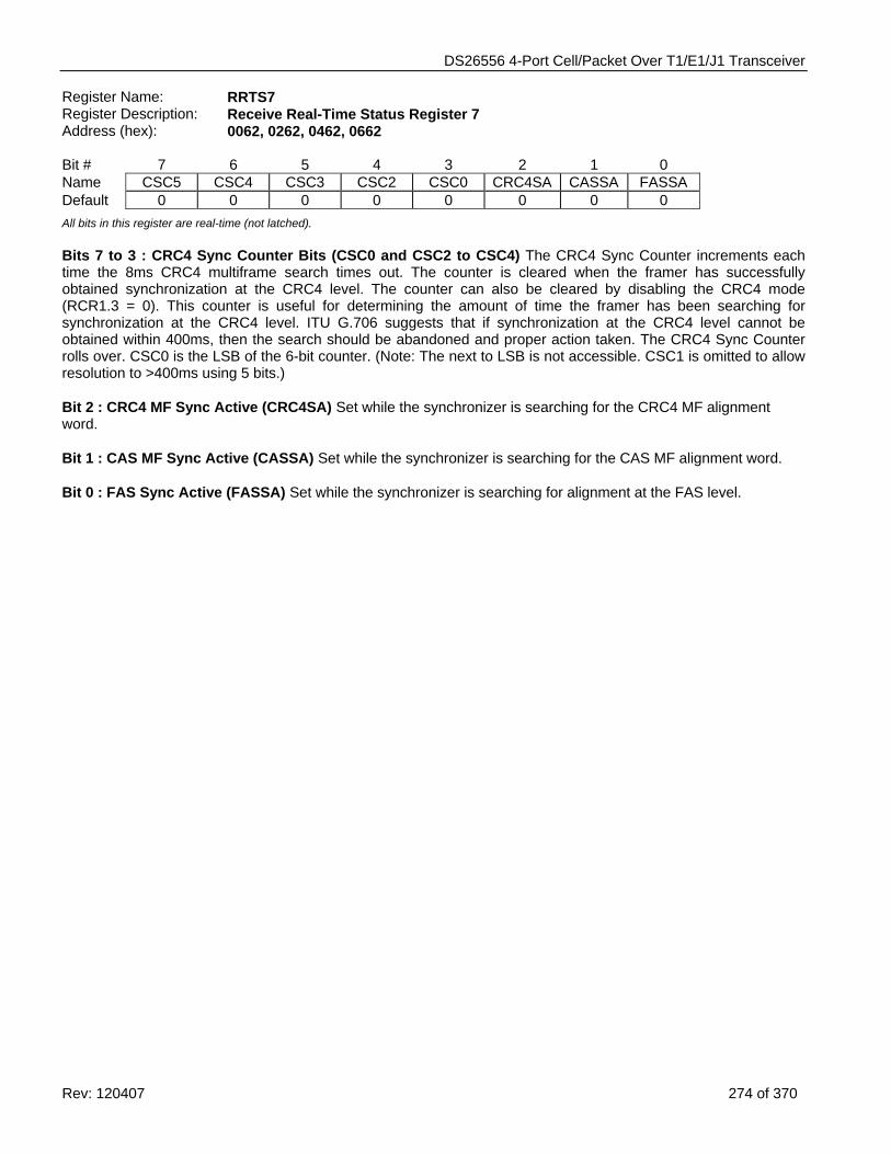
DS26556 4-Port Cell/Packet Over T1/E1/J1 Transceiver
Rev: 120407 274 of 370
Register Name: RRTS7 Register Description: Receive Real-Time Status Register 7 Address (hex): 0062, 0262, 0462, 0662 Bit # 7 6 5 4 3 2 1 0 Name CSC5 CSC4 CSC3 CSC2 CSC0 CRC4SA CASSA FASSA Default 0 0 0 0 0 0 0 0 All bits in this register are real-time (not latched). Bits 7 to 3 : CRC4 Sync Counter Bits (CSC0 and CSC2 to CSC4) The CRC4 Sync Counter increments each time the 8ms CRC4 multiframe search times out. The counter is cleared when the framer has successfully obtained synchronization at the CRC4 level. The counter can also be cleared by disabling the CRC4 mode (RCR1.3 = 0). This counter is useful for determining the amount of time the framer has been searching for synchronization at the CRC4 level. ITU G.706 suggests that if synchronization at the CRC4 level cannot be obtained within 400ms, then the search should be abandoned and proper action taken. The CRC4 Sync Counter rolls over. CSC0 is the LSB of the 6-bit counter. (Note: The next to LSB is not accessible. CSC1 is omitted to allow resolution to >400ms using 5 bits.) Bit 2 : CRC4 MF Sync Active (CRC4SA) Set while the synchronizer is searching for the CRC4 MF alignment word. Bit 1 : CAS MF Sync Active (CASSA) Set while the synchronizer is searching for the CAS MF alignment word. Bit 0 : FAS Sync Active (FASSA) Set while the synchronizer is searching for alignment at the FAS level.
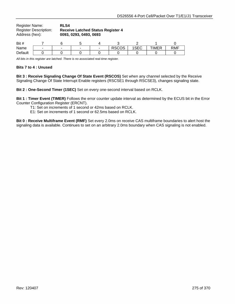
DS26556 4-Port Cell/Packet Over T1/E1/J1 Transceiver
Rev: 120407 275 of 370
Register Name: RLS4 Register Description: Receive Latched Status Register 4 Address (hex): 0093, 0293, 0493, 0693 Bit # 7 6 5 4 3 2 1 0 Name - - - - RSCOS 1SEC TIMER RMF Default 0 0 0 0 0 0 0 0 All bits in this register are latched. There is no associated real-time register. Bits 7 to 4 : Unused Bit 3 : Receive Signaling Change Of State Event (RSCOS) Set when any channel selected by the Receive Signaling Change Of State Interrupt Enable registers (RSCSE1 through RSCSE3), changes signaling state. Bit 2 : One-Second Timer (1SEC) Set on every one-second interval based on RCLK. Bit 1 : Timer Event (TIMER) Follows the error counter update interval as determined by the ECUS bit in the Error Counter Configuration Register (ERCNT).
T1: Set on increments of 1 second or 42ms based on RCLK. E1: Set on increments of 1 second or 62.5ms based on RCLK.
Bit 0 : Receive Multiframe Event (RMF) Set every 2.0ms on receive CAS multiframe boundaries to alert host the signaling data is available. Continues to set on an arbitrary 2.0ms boundary when CAS signaling is not enabled.
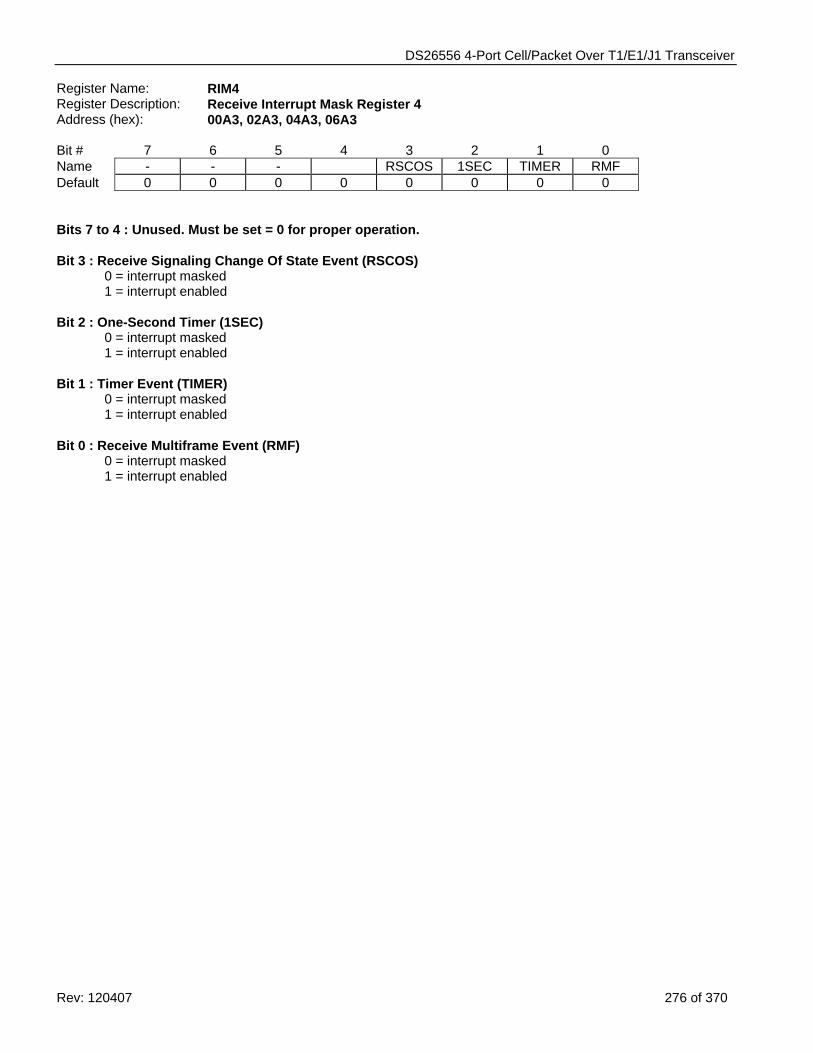
DS26556 4-Port Cell/Packet Over T1/E1/J1 Transceiver
Rev: 120407 276 of 370
Register Name: RIM4 Register Description: Receive Interrupt Mask Register 4 Address (hex): 00A3, 02A3, 04A3, 06A3 Bit # 7 6 5 4 3 2 1 0 Name - - - RSCOS 1SEC TIMER RMF Default 0 0 0 0 0 0 0 0 Bits 7 to 4 : Unused. Must be set = 0 for proper operation. Bit 3 : Receive Signaling Change Of State Event (RSCOS)
0 = interrupt masked 1 = interrupt enabled
Bit 2 : One-Second Timer (1SEC)
0 = interrupt masked 1 = interrupt enabled
Bit 1 : Timer Event (TIMER)
0 = interrupt masked 1 = interrupt enabled
Bit 0 : Receive Multiframe Event (RMF)
0 = interrupt masked 1 = interrupt enabled
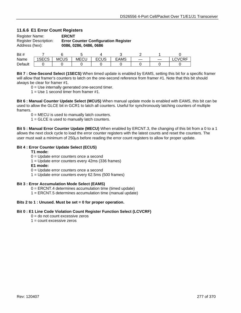
DS26556 4-Port Cell/Packet Over T1/E1/J1 Transceiver
Rev: 120407 277 of 370
11.6.6 E1 Error Count Registers Register Name: ERCNT Register Description: Error Counter Configuration Register Address (hex): 0086, 0286, 0486, 0686 Bit # 7 6 5 4 3 2 1 0 Name 1SECS MCUS MECU ECUS EAMS — — LCVCRF Default 0 0 0 0 0 0 0 0
Bit 7 : One-Second Select (1SECS) When timed update is enabled by EAMS, setting this bit for a specific framer will allow that framer’s counters to latch on the one-second reference from framer #1. Note that this bit should always be clear for framer #1. 0 = Use internally generated one-second timer. 1 = Use 1 second timer from framer #1. Bit 6 : Manual Counter Update Select (MCUS) When manual update mode is enabled with EAMS, this bit can be used to allow the GLCE bit in GCR1 to latch all counters. Useful for synchronously latching counters of multiple framers.
0 = MECU is used to manually latch counters. 1 = GLCE is used to manually latch counters. Bit 5 : Manual Error Counter Update (MECU) When enabled by ERCNT.3, the changing of this bit from a 0 to a 1 allows the next clock cycle to load the error counter registers with the latest counts and reset the counters. The user must wait a minimum of 250μs before reading the error count registers to allow for proper update.
Bit 4 : Error Counter Update Select (ECUS)
T1 mode: 0 = Update error counters once a second 1 = Update error counters every 42ms (336 frames) E1 mode: 0 = Update error counters once a second 1 = Update error counters every 62.5ms (500 frames)
Bit 3 : Error Accumulation Mode Select (EAMS)
0 = ERCNT.4 determines accumulation time (timed update) 1 = ERCNT.5 determines accumulation time (manual update)
Bits 2 to 1 : Unused. Must be set = 0 for proper operation. Bit 0 : E1 Line Code Violation Count Register Function Select (LCVCRF)
0 = do not count excessive zeros 1 = count excessive zeros
DS26556 4-Port Cell/Packet Over T1/E1/J1 Transceiver
Rev: 120407 278 of 370
11.6.6.1 E1 Line Code Violation Count Register (LCVCR) Either bipolar violations or code violations can be counted. Bipolar violations are defined as consecutive marks of the same polarity. In this mode, if the HDB3 mode is set for the receive side, HDB3 codewords are not counted as BPVs. If ERCNT.0 is set, then the LVC counts code violations as defined in ITU O.161. Code violations are defined as consecutive bipolar violations of the same polarity. In most applications, the framer should be programmed to count BPVs when receiving AMI code and to count CVs when receiving HDB3 code. This counter increments at all times and is not disabled by loss of sync conditions. The counter saturates at 65,535 and will not rollover. The bit error rate on an E1 line would have to be greater than 10** - 2 before the VCR would saturate. See Table 11-17.
Table 11-17 E1 Line Code Violation Counting Options E1 CODE VIOLATION SELECT
(ERCNT.0) WHAT IS COUNTED IN THE LCVCRs
0 BPVs 1 CVs
Register Name: LCVCR1 Register Description: Line Code Violation Count Register 1 Address (hex): 0050, 0250, 0450, 0650 Bit # 7 6 5 4 3 2 1 0 Name LCVC15 LCVC14 LCVC13 LCVC12 LCVC11 LCVC10 LCVC9 LCCV8 Default 0 0 0 0 0 0 0 0 Bits 7 to 0 : Line Code Violation Counter Bits 15 to 8 (LCVC15 to LCVC8). LCV15 is the MSB of the 16-bit code violation count. Register Name: LCVCR2 Register Description: Line Code Violation Count Register 2 Address (hex): 0051, 0251, 0451, 0651 Bit # 7 6 5 4 3 2 1 0 Name LCVC7 LCVC6 LCVC5 LCVC4 LCVC3 LCVC2 LCVC1 LCVC0 Default 0 0 0 0 0 0 0 0 Bits 7 to 0 : Line Code Violation Counter Bits 7 to 0 (LCVC7 to LCVC0) LCV0 is the LSB of the 16-bit code violation count.
11.6.6.2 E1 Path Code Violation Count Register (PCVCR) In E1 operation, the Path Code Violation Count register records CRC4 errors. Since the maximum CRC4 count in a one-second period is 1000, this counter cannot saturate. The counter is disabled during loss of sync at either the FAS or CRC4 level; it will continue to count if loss of multiframe sync occurs at the CAS level.
The Path Code Violation Count Register 1 (PCVCR1) is the most significant word and PCVCR2 is the least significant word of a 16-bit counter that records path violations (PVs).
DS26556 4-Port Cell/Packet Over T1/E1/J1 Transceiver
Rev: 120407 279 of 370
Register Name: PCVCR1 Register Description: Path Code Violation Count Register 1 Address (hex): 0052, 0252, 0452, 0652 Bit # 7 6 5 4 3 2 1 0 Name PCVC15 PCVC1
4 PCVC1
3 PCVC1
2 PCVC1
1 PCVC1
0 PCVC9 PCVC8
Default 0 0 0 0 0 0 0 0 Bits 7 to 0 : Path Code Violation Counter Bits 15 to 8 (PCVC15 to PCVC8) PCVC15 is the MSB of the 16-bit path code violation count. Register Name: PCVCR2 Register Description: Path Code Violation Count Register 2 Address (hex): 0053, 0253, 0453, 0653 Bit # 7 6 5 4 3 2 1 0 Name PCVC7 PCVC6 PCVC5 PCVC4 PCVC3 PCVC2 PCVC1 PCVC0 Default 0 0 0 0 0 0 0 0 Bits 7 to 0 : Path Code Violation Counter Bits 7 to 0 (PCVC7 to PCVC0) PCVC0 is the LSB of the 16-bit path code violation count.
11.6.6.3 E1 Frames Out-of-Sync Count Register (FOSCR) In E1 mode, the FOSCR counts word errors in the Frame Alignment Signal in time slot 0. This counter is disabled when RLOF is high. FAS errors will not be counted when the framer is searching for FAS alignment and/or synchronization at either the CAS or CRC4 multiframe level. Since the maximum FAS word error count in a one-second period is 4000, this counter cannot saturate.
The Frames Out of Sync Count Register 1 (FOSCR1) is the most significant word and FOSCR2 is the least significant word of a 16-bit counter that records frames out of sync. Register Name: FOSCR1 Register Description: Frames Out Of Sync Count Register 1 Address (hex): 0054, 0254, 0454, 0654 Bit # 7 6 5 4 3 2 1 0 Name FOS15 FOS14 FOS13 FOS12 FOS11 FOS10 FOS9 FOS8 Default 0 0 0 0 0 0 0 0 Bits 7 to 0 : Frames Out of Sync Counter Bits 15 to 8 (FOS15 to FOS8) FOS15 is the MSB of the 16-bit frames out of sync count. Register Name: FOSCR2 Register Description: Frames Out Of Sync Count Register 2 Address (hex): 0055, 0255, 0455, 0655 Bit # 7 6 5 4 3 2 1 0 Name FOS7 FOS6 FOS5 FOS4 FOS3 FOS2 FOS1 FOS0 Default 0 0 0 0 0 0 0 0 Bits 7 to 0 : Frames Out of Sync Counter Bits 7 to 0 (FOS7 to FOS0) FOS0 is the LSB of the 16-bit frames out of sync count.
DS26556 4-Port Cell/Packet Over T1/E1/J1 Transceiver
Rev: 120407 280 of 370
11.6.6.4 E-Bit Counter (EBCR) This counter is only available in E1 mode. E–bit Count Register 1 (EBCR1) is the most significant word and EBCR2 is the least significant word of a 16-bit counter that records Far End Block Errors (FEBE) as reported in the first bit of frames 13 and 15 on E1 lines running with CRC4 multiframe. These count registers will increment once each time the received E-bit is set to zero. Since the maximum E-bit count in a one second period is 1000, this counter cannot saturate. The counter is disabled during loss of sync at either the FAS or CRC4 level; it will continue to count if loss of multiframe sync occurs at the CAS level. Register Name: EBCR1 Register Description: E–Bit Count Register 1 Address (hex): 0056, 0256, 0456, 0656 Bit # 7 6 5 4 3 2 1 0 Name EB15 EB14 EB13 EB12 EB11 EB10 EB9 EB8 Default 0 0 0 0 0 0 0 0 Bits 7 to 0 : E-Bit Counter Bits 15 to 8 (EB15 to EB8) EB15 is the MSB of the 16-bit E-Bit count. Register Name: EBCR2 Register Description: E–Bit Count Register 2 Address (hex): 0057, 0257, 0457, 0657 Bit # 7 6 5 4 3 2 1 0 Name EB7 EB6 EB5 EB4 EB3 EB2 EB1 EB0 Default 0 0 0 0 0 0 0 0 Bits 7 to 0 : E-Bit Counter Bits 7 to 0 (EB7 to EB0) EB0 is the LSB of the 16-bit E-Bit count.
11.6.7 DS0 Monitoring Function Register Name: RDS0SEL Register Description: Receive Channel Monitor Select Address (hex): 0012, 0212, 0412, 0612 Bit # 7 6 5 4 3 2 1 0 Name — — — RCM4 RCM3 RCM2 RCM1 RCM0 Default 0 0 0 0 0 0 0 0 Bits 7 to 5 : Unused. Must be set = 0 for proper operation. Bits 4 to 0 : Receive Channel Monitor Bits (RCM4 to RCM0) RCM0 is the LSB of a 5-bit channel select that determines which receive DS0 channel data will appear in the RDS0M register. Register Name: RDS0M Register Description: Receive DS0 Monitor Register Address (hex): 0060, 0260, 0460, 0660 Bit # 7 6 5 4 3 2 1 0 Name B1 B2 B3 B4 B5 B6 B7 B8 Default 0 0 0 0 0 0 0 0 Bits 7 to 0 : Receive DS0 Channel Bits (B1 to B8) Receive channel data that has been selected by the Receive Channel Monitor Select Register. B8 is the LSB of the DS0 channel (last bit to be received).
DS26556 4-Port Cell/Packet Over T1/E1/J1 Transceiver
Rev: 120407 281 of 370
11.6.8 E1 Receive Signaling Operation Register Name: RSIGC Register Description: Receive Signaling Control Register Address (hex): 0013, 0213, 0413, 0613 Bit # 7 6 5 4 3 2 1 0 Name — — — CASMS — - - - Default 0 0 0 0 0 0 0 0 Bits 7 to 5 : Unused. Must be set = 0 for proper operation. Bit 4 : CAS Mode Select (CASMS)
0 = The DS26556 will initiate a resync when two consecutive multiframe alignment signals have been received with an error.
1 = The DS26556 will initiate a resync when two consecutive multiframe alignment signals have been received with an error, or 1 multiframe has been received with all the bits in time slot 16
in state 0. Alignment criteria are met when at least one bit in state 1 is present in the time slot
16 preceding the multiframe alignment signal first detected (G.732 alternate criteria).
Bit 3 to 0 : Unused. Must be set = 0 for proper operation.
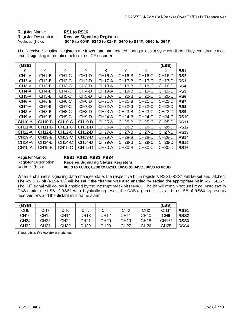
DS26556 4-Port Cell/Packet Over T1/E1/J1 Transceiver
Rev: 120407 282 of 370
Register Name: RS1 to RS16 Register Description: Receive Signaling Registers Address (hex): 0040 to 004F, 0240 to 024F, 0440 to 044F, 0640 to 064F The Receive Signaling Registers are frozen and not updated during a loss of sync condition. They contain the most recent signaling information before the LOF occurred. (MSB) (LSB)
0 0 0 0 X Y X X RS1 CH1-A CH1-B CH1-C CH1-D CH16-A CH16-B CH16-C CH16-D RS2 CH2-A CH2-B CH2-C CH2-D CH17-A CH17-B CH17-C CH17-D RS3 CH3-A CH3-B CH3-C CH3-D CH18-A CH18-B CH18-C CH18-D RS4 CH4-A CH4-B CH4-C CH4-D CH19-A CH19-B CH19-C CH19-D RS5 CH5-A CH5-B CH5-C CH5-D CH20-A CH20-B CH20-C CH20-D RS6 CH6-A CH6-B CH6-C CH6-D CH21-A CH21-B CH21-C CH21-D RS7 CH7-A CH7-B CH7-C CH7-D CH22-A CH22-B CH22-C CH22-D RS8 CH8-A CH8-B CH8-C CH8-D CH23-A CH23-B CH23-C CH23-D RS9 CH9-A CH9-B CH9-C CH9-D CH24-A CH24-B CH24-C CH24-D RS10
CH10-A CH10-B CH10-C CH10-D CH25-A CH25-B CH25-C CH25-D RS11 CH11-A CH11-B CH11-C CH11-D CH26-A CH26-B CH26-C CH26-D RS12 CH12-A CH12-B CH12-C CH12-D CH27-A CH27-B CH27-C CH27-D RS13 CH13-A CH13-B CH13-C CH13-D CH28-A CH28-B CH28-C CH28-D RS14 CH14-A CH14-B CH14-C CH14-D CH29-A CH29-B CH29-C CH29-D RS15 CH15-A CH15-B CH15-C CH15-D CH30-A CH30-B CH30-C CH30-D RS16 Register Name: RSS1, RSS2, RSS3, RSS4 Register Description: Receive Signaling Status Registers Address (hex): 0098 to 009B, 0298 to 029B, 0498 to 049B, 0698 to 069B When a channel’s signaling data changes state, the respective bit in registers RSS1-RSS4 will be set and latched. The RSCOS bit (RLSR4.3) will be set if the channel was also enabled by setting the appropriate bit in RSCSE1-4. The INT signal will go low if enabled by the interrupt mask bit RIM4.3. The bit will remain set until read. Note that in CAS mode, the LSB of RSS1 would typically represent the CAS alignment bits, and the LSB of RSS3 represents reserved bits and the distant multiframe alarm. (MSB) (LSB) CH8 CH7 CH6 CH5 CH4 CH3 CH2 CH1* RSS1 CH16 CH15 CH14 CH13 CH12 CH11 CH10 CH9 RSS2 CH24 CH23 CH22 CH21 CH20 CH19 CH18 CH17* RSS3 CH32 CH31 CH30 CH29 CH28 CH27 CH26 CH25 RSS4
Status bits in this register are latched.
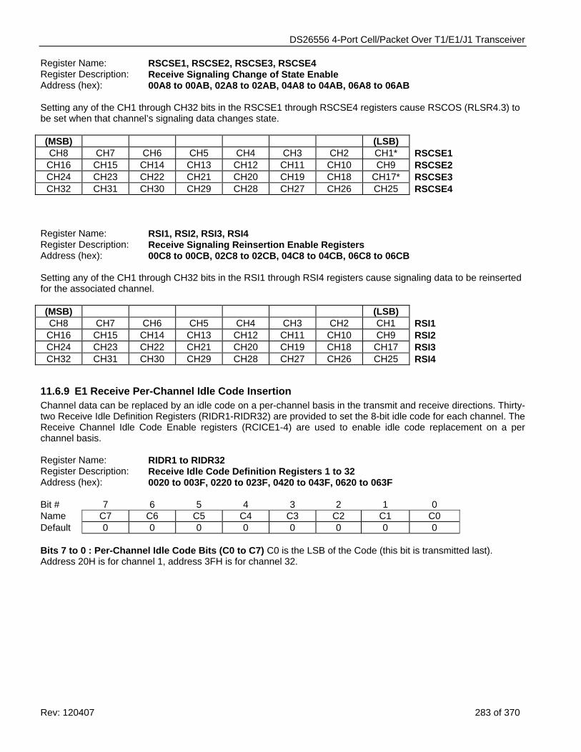
DS26556 4-Port Cell/Packet Over T1/E1/J1 Transceiver
Rev: 120407 283 of 370
Register Name: RSCSE1, RSCSE2, RSCSE3, RSCSE4 Register Description: Receive Signaling Change of State Enable Address (hex): 00A8 to 00AB, 02A8 to 02AB, 04A8 to 04AB, 06A8 to 06AB Setting any of the CH1 through CH32 bits in the RSCSE1 through RSCSE4 registers cause RSCOS (RLSR4.3) to be set when that channel’s signaling data changes state. (MSB) (LSB) CH8 CH7 CH6 CH5 CH4 CH3 CH2 CH1* RSCSE1 CH16 CH15 CH14 CH13 CH12 CH11 CH10 CH9 RSCSE2 CH24 CH23 CH22 CH21 CH20 CH19 CH18 CH17* RSCSE3 CH32 CH31 CH30 CH29 CH28 CH27 CH26 CH25 RSCSE4
Register Name: RSI1, RSI2, RSI3, RSI4 Register Description: Receive Signaling Reinsertion Enable Registers Address (hex): 00C8 to 00CB, 02C8 to 02CB, 04C8 to 04CB, 06C8 to 06CB Setting any of the CH1 through CH32 bits in the RSI1 through RSI4 registers cause signaling data to be reinserted for the associated channel. (MSB) (LSB) CH8 CH7 CH6 CH5 CH4 CH3 CH2 CH1 RSI1 CH16 CH15 CH14 CH13 CH12 CH11 CH10 CH9 RSI2 CH24 CH23 CH22 CH21 CH20 CH19 CH18 CH17 RSI3 CH32 CH31 CH30 CH29 CH28 CH27 CH26 CH25 RSI4
11.6.9 E1 Receive Per-Channel Idle Code Insertion Channel data can be replaced by an idle code on a per-channel basis in the transmit and receive directions. Thirty-two Receive Idle Definition Registers (RIDR1-RIDR32) are provided to set the 8-bit idle code for each channel. The Receive Channel Idle Code Enable registers (RCICE1-4) are used to enable idle code replacement on a per channel basis. Register Name: RIDR1 to RIDR32 Register Description: Receive Idle Code Definition Registers 1 to 32 Address (hex): 0020 to 003F, 0220 to 023F, 0420 to 043F, 0620 to 063F Bit # 7 6 5 4 3 2 1 0 Name C7 C6 C5 C4 C3 C2 C1 C0 Default 0 0 0 0 0 0 0 0 Bits 7 to 0 : Per-Channel Idle Code Bits (C0 to C7) C0 is the LSB of the Code (this bit is transmitted last). Address 20H is for channel 1, address 3FH is for channel 32.
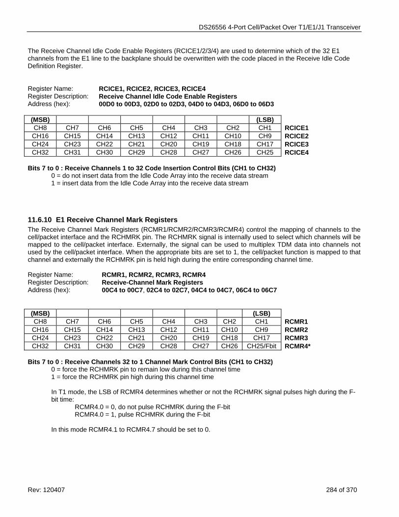
DS26556 4-Port Cell/Packet Over T1/E1/J1 Transceiver
Rev: 120407 284 of 370
The Receive Channel Idle Code Enable Registers (RCICE1/2/3/4) are used to determine which of the 32 E1 channels from the E1 line to the backplane should be overwritten with the code placed in the Receive Idle Code Definition Register. Register Name: RCICE1, RCICE2, RCICE3, RCICE4 Register Description: Receive Channel Idle Code Enable Registers Address (hex): 00D0 to 00D3, 02D0 to 02D3, 04D0 to 04D3, 06D0 to 06D3 (MSB) (LSB) CH8 CH7 CH6 CH5 CH4 CH3 CH2 CH1 RCICE1 CH16 CH15 CH14 CH13 CH12 CH11 CH10 CH9 RCICE2 CH24 CH23 CH22 CH21 CH20 CH19 CH18 CH17 RCICE3 CH32 CH31 CH30 CH29 CH28 CH27 CH26 CH25 RCICE4
Bits 7 to 0 : Receive Channels 1 to 32 Code Insertion Control Bits (CH1 to CH32)
0 = do not insert data from the Idle Code Array into the receive data stream 1 = insert data from the Idle Code Array into the receive data stream
11.6.10 E1 Receive Channel Mark Registers The Receive Channel Mark Registers (RCMR1/RCMR2/RCMR3/RCMR4) control the mapping of channels to the cell/packet interface and the RCHMRK pin. The RCHMRK signal is internally used to select which channels will be mapped to the cell/packet interface. Externally, the signal can be used to multiplex TDM data into channels not used by the cell/packet interface. When the appropriate bits are set to 1, the cell/packet function is mapped to that channel and externally the RCHMRK pin is held high during the entire corresponding channel time. Register Name: RCMR1, RCMR2, RCMR3, RCMR4 Register Description: Receive-Channel Mark Registers Address (hex): 00C4 to 00C7, 02C4 to 02C7, 04C4 to 04C7, 06C4 to 06C7 (MSB) (LSB) CH8 CH7 CH6 CH5 CH4 CH3 CH2 CH1 RCMR1 CH16 CH15 CH14 CH13 CH12 CH11 CH10 CH9 RCMR2 CH24 CH23 CH22 CH21 CH20 CH19 CH18 CH17 RCMR3 CH32 CH31 CH30 CH29 CH28 CH27 CH26 CH25/Fbit RCMR4*
Bits 7 to 0 : Receive Channels 32 to 1 Channel Mark Control Bits (CH1 to CH32)
0 = force the RCHMRK pin to remain low during this channel time 1 = force the RCHMRK pin high during this channel time
In T1 mode, the LSB of RCMR4 determines whether or not the RCHMRK signal pulses high during the F-bit time:
RCMR4.0 = 0, do not pulse RCHMRK during the F-bit RCMR4.0 = 1, pulse RCHMRK during the F-bit
In this mode RCMR4.1 to RCMR4.7 should be set to 0.
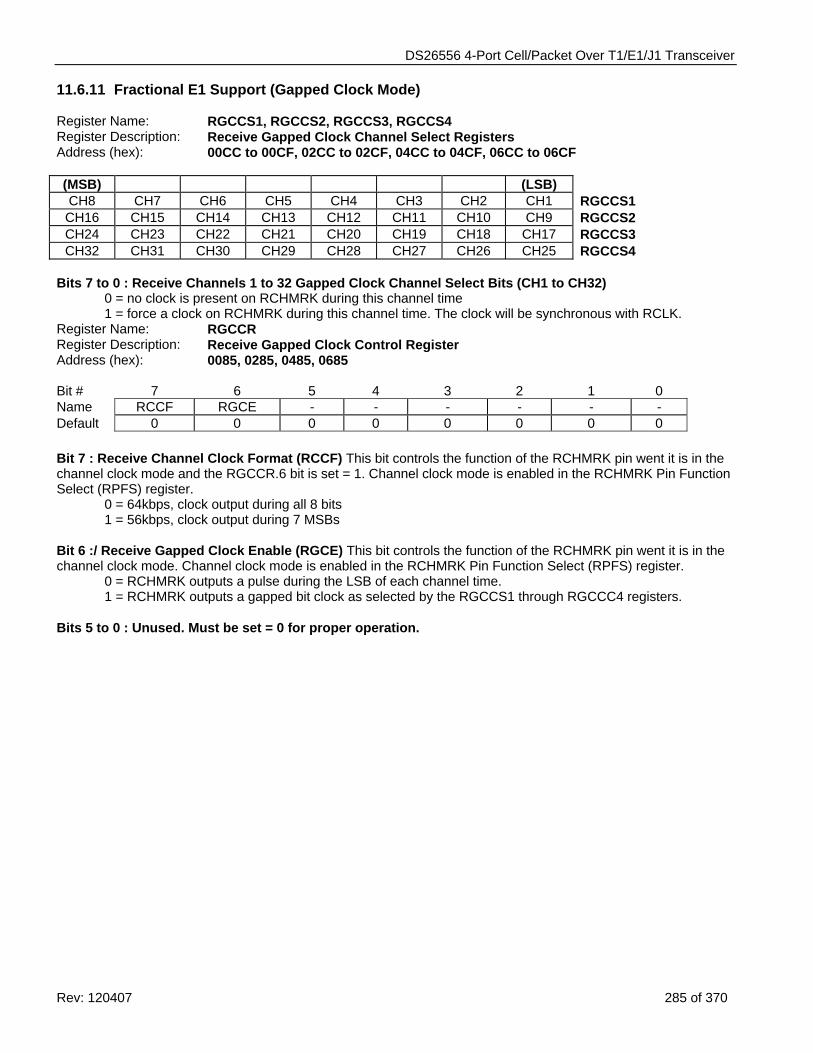
DS26556 4-Port Cell/Packet Over T1/E1/J1 Transceiver
Rev: 120407 285 of 370
11.6.11 Fractional E1 Support (Gapped Clock Mode) Register Name: RGCCS1, RGCCS2, RGCCS3, RGCCS4 Register Description: Receive Gapped Clock Channel Select Registers Address (hex): 00CC to 00CF, 02CC to 02CF, 04CC to 04CF, 06CC to 06CF (MSB) (LSB) CH8 CH7 CH6 CH5 CH4 CH3 CH2 CH1 RGCCS1 CH16 CH15 CH14 CH13 CH12 CH11 CH10 CH9 RGCCS2 CH24 CH23 CH22 CH21 CH20 CH19 CH18 CH17 RGCCS3 CH32 CH31 CH30 CH29 CH28 CH27 CH26 CH25 RGCCS4
Bits 7 to 0 : Receive Channels 1 to 32 Gapped Clock Channel Select Bits (CH1 to CH32)
0 = no clock is present on RCHMRK during this channel time 1 = force a clock on RCHMRK during this channel time. The clock will be synchronous with RCLK.
Register Name: RGCCR Register Description: Receive Gapped Clock Control Register Address (hex): 0085, 0285, 0485, 0685 Bit # 7 6 5 4 3 2 1 0 Name RCCF RGCE - - - - - - Default 0 0 0 0 0 0 0 0 Bit 7 : Receive Channel Clock Format (RCCF) This bit controls the function of the RCHMRK pin went it is in the channel clock mode and the RGCCR.6 bit is set = 1. Channel clock mode is enabled in the RCHMRK Pin Function Select (RPFS) register.
0 = 64kbps, clock output during all 8 bits 1 = 56kbps, clock output during 7 MSBs
Bit 6 :/ Receive Gapped Clock Enable (RGCE) This bit controls the function of the RCHMRK pin went it is in the channel clock mode. Channel clock mode is enabled in the RCHMRK Pin Function Select (RPFS) register.
0 = RCHMRK outputs a pulse during the LSB of each channel time. 1 = RCHMRK outputs a gapped bit clock as selected by the RGCCS1 through RGCCC4 registers.
Bits 5 to 0 : Unused. Must be set = 0 for proper operation.
DS26556 4-Port Cell/Packet Over T1/E1/J1 Transceiver
Rev: 120407 286 of 370
11.6.12 Additional Sa-Bit and Si-Bit Receive Operation (E1 Mode) Register Name: RAF Register Description: Receive Align Frame Register Address (hex): 0064, 0264, 0464, 0664 Bit # 7 6 5 4 3 2 1 0 Name Si 0 0 1 1 0 1 1 Default 0 0 0 0 0 0 0 0 Bit 7 : International Bit (Si) Bit 6 : Frame Alignment Signal Bit (0) Bit 5 : Frame Alignment Signal Bit (0) Bit 4 : Frame Alignment Signal Bit (1) Bit 3 : Frame Alignment Signal Bit (1) Bit 2 : Frame Alignment Signal Bit (0) Bit 1 : Frame Alignment Signal Bit (1) Bit 0 : Frame Alignment Signal Bit (1)
DS26556 4-Port Cell/Packet Over T1/E1/J1 Transceiver
Rev: 120407 287 of 370
Register Name: RNAF Register Description: Receive Non-Align Frame Register Address (hex): 0065, 0256, 0456, 0665 Bit # 7 6 5 4 3 2 1 0 Name Si 1 A Sa4 Sa5 Sa6 Sa7 Sa8 Default 0 0 0 0 0 0 0 0 Bit 7 : International Bit (Si) Bit 6 : Frame Non-Alignment Signal Bit (1) Bit 5 : Remote Alarm (A) Bit 4 : Additional Bit 4 (Sa4) Bit 3 : Additional Bit 5 (Sa5) Bit 2 : Additional Bit 6 (Sa6) Bit 1 : Additional Bit 7 (Sa7) Bit 0 : Additional Bit 8 (Sa8) Register Name: RsiAF Register Description: Received Si Bits of the Align Frame Address (hex): 0066, 0266, 0466, 0666 Bit # 7 6 5 4 3 2 1 0 Name SiF14 SiF12 SiF10 SiF8 SiF6 SiF4 SiF2 SiF0 Default 0 0 0 0 0 0 0 0 Bit 0 : Si Bit of Frame 0 (SiF0) Bit 1 : Si Bit of Frame 2 (SiF2) Bit 2 : Si Bit of Frame 4 (SiF4) Bit 3 : Si Bit of Frame 6 (SiF6) Bit 4 : Si Bit of Frame 8 (SiF8) Bit 5 : Si Bit of Frame 10 (SiF10) Bit 6 : Si Bit of Frame 12 (SiF12) Bit 7 : Si Bit of Frame 14 (SiF14)
DS26556 4-Port Cell/Packet Over T1/E1/J1 Transceiver
Rev: 120407 288 of 370
Register Name: RSiNAF Register Description: Received Si Bits of the Non-Align Frame Address (hex): 0067, 0267, 0467, 0667 Bit # 7 6 5 4 3 2 1 0 Name SiF15 SiF13 SiF11 SiF9 SiF7 SiF5 SiF3 SiF1 Default 0 0 0 0 0 0 0 0 Bit 7 : Si Bit of Frame 15 (SiF15) Bit 6 : Si Bit of Frame 13 (SiF13) Bit 5 : Si Bit of Frame 11 (SiF11) Bit 4 : Si Bit of Frame 9 (SiF9) Bit 3 : Si Bit of Frame 7 (SiF7) Bit 2 : Si Bit of Frame 5 (SiF5) Bit 1 : Si Bit of Frame 3 (SiF3) Bit 0 : Si Bit of Frame 1 (SiF1) Register Name: RRA Register Description: Received Remote Alarm Address (hex): 0068, 0268, 0468, 0668 Bit # 7 6 5 4 3 2 1 0 Name RRAF1
5 RRAF1
3 RRAF1
1 RRAF9 RRAF7 RRAF5 RRAF3 RRAF1
Default 0 0 0 0 0 0 0 0 Bit 7 : Remote Alarm Bit of Frame 15 (RRAF15) Bit 6 : Remote Alarm Bit of Frame 13 (RRAF13) Bit 5 : Remote Alarm Bit of Frame 11 (RRAF11) Bit 4 : Remote Alarm Bit of Frame 9 (RRAF9) Bit 3 : Remote Alarm Bit of Frame 7 (RRAF7) Bit 2 : Remote Alarm Bit of Frame 5 (RRAF5) Bit 1 : Remote Alarm Bit of Frame 3 (RRAF3) Bit 0 : Remote Alarm Bit of Frame 1 (RRAF1)
DS26556 4-Port Cell/Packet Over T1/E1/J1 Transceiver
Rev: 120407 289 of 370
Register Name: RSa4 Register Description: Received Sa4 Bits Address (hex): 0069, 0269, 0469, 0669 Bit # 7 6 5 4 3 2 1 0 Name RSa4F15 RSa4F13 RSa4F11 RSa4F9 RSa4F7 RSa4F5 RSa4F3 RSa4F1 Default 0 0 0 0 0 0 0 0 Bit 7 : Sa4 Bit of Frame 15 (RSa4F15) Bit 6 : Sa4 Bit of Frame 13 (RSa4F13) Bit 5 : Sa4 Bit of Frame 11 (RSa4F11) Bit 4 : Sa4 Bit of Frame 9 (RSa4F9) Bit 3 : Sa4 Bit of Frame 7 (RSa4F7) Bit 2 : Sa4 Bit of Frame 5 (RSa4F5) Bit 1 : Sa4 Bit of Frame 3 (RSa4F3) Bit 0 : Sa4 Bit of Frame 1 (RSa4F1) Register Name: RSa5 Register Description: Received Sa5 Bits Address (hex): 006A, 026A, 046A, 066A Bit # 7 6 5 4 3 2 1 0 Name RSa5F15 RSa5F13 RSa5F11 RSa5F9 RSa5F7 RSa5F5 RSa5F3 RSa5F1 Default 0 0 0 0 0 0 0 0 Bit 7 : Sa5 Bit of Frame 15 (RSa5F15) Bit 6 : Sa5 Bit of Frame 13 (RSa5F13) Bit 5 : Sa5 Bit of Frame 11 (RSa5F11) Bit 4 : Sa5 Bit of Frame 9 (RSa5F9) Bit 3 : Sa5 Bit of Frame 7 (RSa5F7) Bit 2 : Sa5 Bit of Frame 5 (RSa5F5) Bit 1 : Sa5 Bit of Frame 3 (RSa5F3) Bit 0 : Sa5 Bit of Frame 1 (RSa5F1

DS26556 4-Port Cell/Packet Over T1/E1/J1 Transceiver
Rev: 120407 290 of 370
Register Name: RSa6 Register Description: Received Sa6 Bits Address (hex): 006B, 026B, 046B, 066B Bit # 7 6 5 4 3 2 1 0 Name RSa6F15 RSa6F13 RSa6F11 RSa6F9 RSa6F7 RSa6F5 RSa6F3 RSa6F1 Default 0 0 0 0 0 0 0 0 Bit 7 : Sa6 Bit of Frame 15 (RSa6F15) Bit 6 : Sa6 Bit of Frame 13 (RSa6F13) Bit 5 : Sa6 Bit of Frame 11 (RSa6F11) Bit 4 : Sa6 Bit of Frame 9 (RSa6F9) Bit 3 : Sa6 Bit of Frame 7 (RSa6F7) Bit 2 : Sa6 Bit of Frame 5 (RSa6F5) Bit 1 : Sa6 Bit of Frame 3 (RSa6F3) Bit 0 : Sa6 Bit of Frame 1 (RSa6F1) Register Name: RSa7 Register Description: Received Sa7 Bits Address (hex): 006C, 026C, 046C, 066C Bit # 7 6 5 4 3 2 1 0 Name RSa7F15 RSa7F13 RSa7F11 RSa7F9 RSa7F7 RSa7F5 RSa7F3 RSa7F1 Default 0 0 0 0 0 0 0 0 Bit 7 : Sa7 Bit of Frame 15 (RSa4F15) Bit 6 : Sa7 Bit of Frame 13 (RSa7F13) Bit 5 : Sa7 Bit of Frame 11 (RSa7F11) Bit 4 : Sa7 Bit of Frame 9 (RSa7F9) Bit 3 : Sa7 Bit of Frame 7 (RSa7F7) Bit 2 : Sa7 Bit of Frame 5 (RSa7F5) Bit 1 : Sa7 Bit of Frame 3 (RSa7F3) Bit 0 : Sa7 Bit of Frame 1 (RSa7F1)
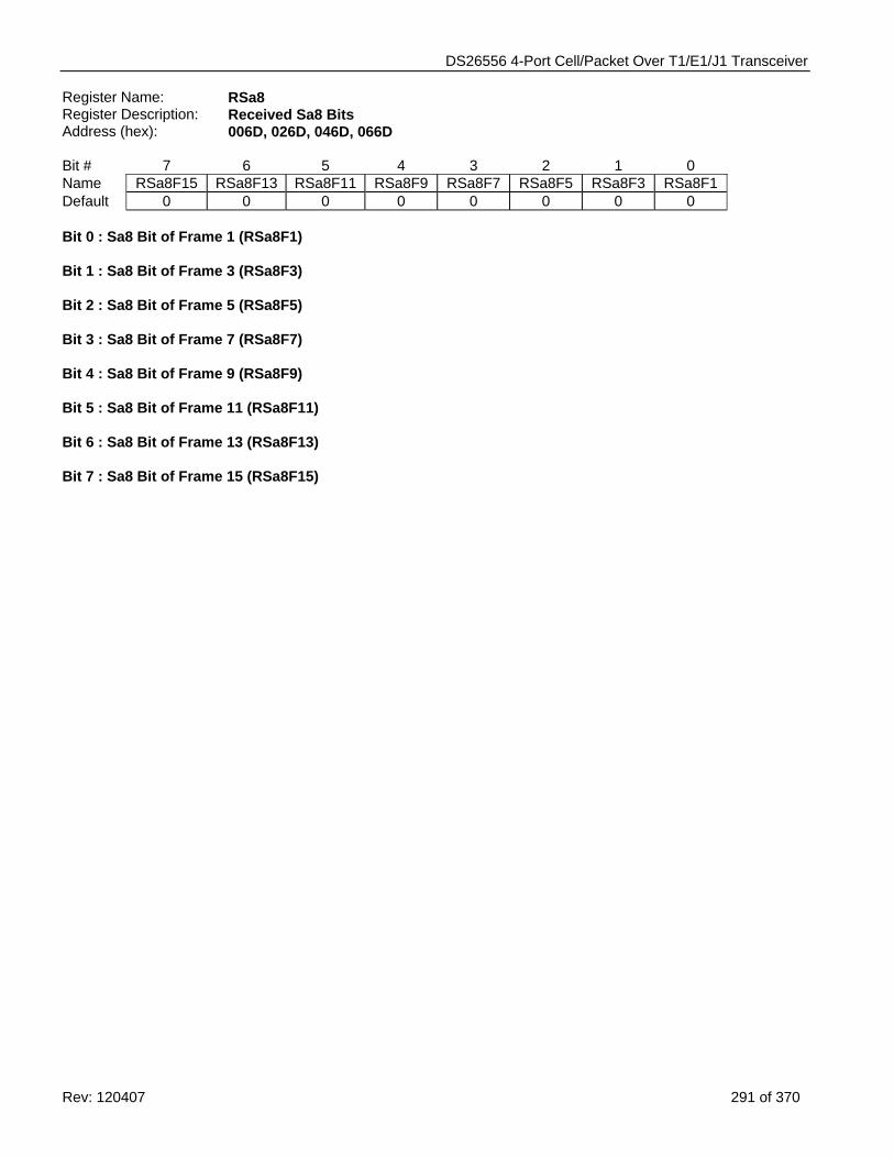
DS26556 4-Port Cell/Packet Over T1/E1/J1 Transceiver
Rev: 120407 291 of 370
Register Name: RSa8 Register Description: Received Sa8 Bits Address (hex): 006D, 026D, 046D, 066D Bit # 7 6 5 4 3 2 1 0 Name RSa8F15 RSa8F13 RSa8F11 RSa8F9 RSa8F7 RSa8F5 RSa8F3 RSa8F1 Default 0 0 0 0 0 0 0 0 Bit 0 : Sa8 Bit of Frame 1 (RSa8F1) Bit 1 : Sa8 Bit of Frame 3 (RSa8F3) Bit 2 : Sa8 Bit of Frame 5 (RSa8F5) Bit 3 : Sa8 Bit of Frame 7 (RSa8F7) Bit 4 : Sa8 Bit of Frame 9 (RSa8F9) Bit 5 : Sa8 Bit of Frame 11 (RSa8F11) Bit 6 : Sa8 Bit of Frame 13 (RSa8F13) Bit 7 : Sa8 Bit of Frame 15 (RSa8F15)
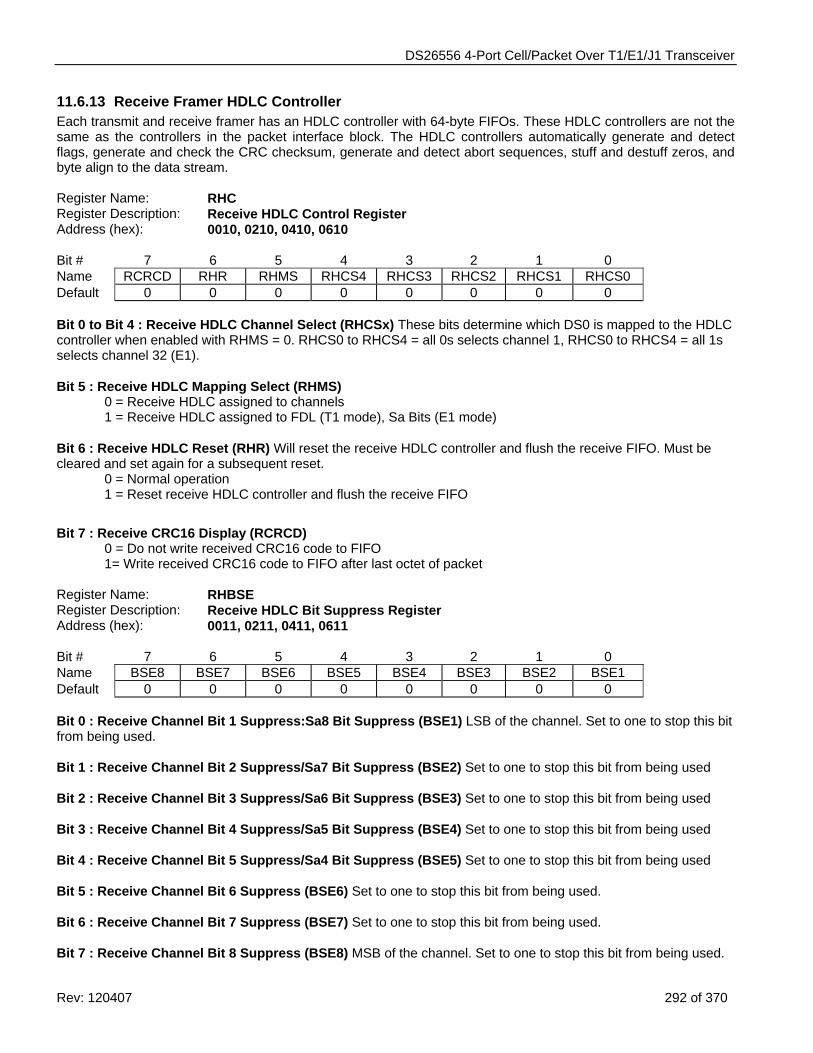
DS26556 4-Port Cell/Packet Over T1/E1/J1 Transceiver
Rev: 120407 292 of 370
11.6.13 Receive Framer HDLC Controller Each transmit and receive framer has an HDLC controller with 64-byte FIFOs. These HDLC controllers are not the same as the controllers in the packet interface block. The HDLC controllers automatically generate and detect flags, generate and check the CRC checksum, generate and detect abort sequences, stuff and destuff zeros, and byte align to the data stream. Register Name: RHC Register Description: Receive HDLC Control Register Address (hex): 0010, 0210, 0410, 0610 Bit # 7 6 5 4 3 2 1 0 Name RCRCD RHR RHMS RHCS4 RHCS3 RHCS2 RHCS1 RHCS0 Default 0 0 0 0 0 0 0 0 Bit 0 to Bit 4 : Receive HDLC Channel Select (RHCSx) These bits determine which DS0 is mapped to the HDLC controller when enabled with RHMS = 0. RHCS0 to RHCS4 = all 0s selects channel 1, RHCS0 to RHCS4 = all 1s selects channel 32 (E1). Bit 5 : Receive HDLC Mapping Select (RHMS)
0 = Receive HDLC assigned to channels 1 = Receive HDLC assigned to FDL (T1 mode), Sa Bits (E1 mode)
Bit 6 : Receive HDLC Reset (RHR) Will reset the receive HDLC controller and flush the receive FIFO. Must be cleared and set again for a subsequent reset.
0 = Normal operation 1 = Reset receive HDLC controller and flush the receive FIFO
Bit 7 : Receive CRC16 Display (RCRCD) 0 = Do not write received CRC16 code to FIFO 1= Write received CRC16 code to FIFO after last octet of packet Register Name: RHBSE Register Description: Receive HDLC Bit Suppress Register Address (hex): 0011, 0211, 0411, 0611 Bit # 7 6 5 4 3 2 1 0 Name BSE8 BSE7 BSE6 BSE5 BSE4 BSE3 BSE2 BSE1 Default 0 0 0 0 0 0 0 0 Bit 0 : Receive Channel Bit 1 Suppress:Sa8 Bit Suppress (BSE1) LSB of the channel. Set to one to stop this bit from being used. Bit 1 : Receive Channel Bit 2 Suppress/Sa7 Bit Suppress (BSE2) Set to one to stop this bit from being used Bit 2 : Receive Channel Bit 3 Suppress/Sa6 Bit Suppress (BSE3) Set to one to stop this bit from being used Bit 3 : Receive Channel Bit 4 Suppress/Sa5 Bit Suppress (BSE4) Set to one to stop this bit from being used Bit 4 : Receive Channel Bit 5 Suppress/Sa4 Bit Suppress (BSE5) Set to one to stop this bit from being used Bit 5 : Receive Channel Bit 6 Suppress (BSE6) Set to one to stop this bit from being used. Bit 6 : Receive Channel Bit 7 Suppress (BSE7) Set to one to stop this bit from being used. Bit 7 : Receive Channel Bit 8 Suppress (BSE8) MSB of the channel. Set to one to stop this bit from being used.
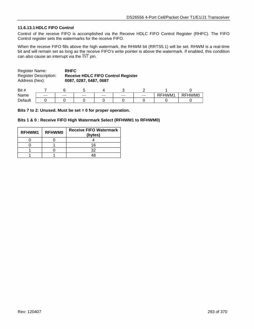
DS26556 4-Port Cell/Packet Over T1/E1/J1 Transceiver
Rev: 120407 293 of 370
11.6.13.1 HDLC FIFO Control Control of the receive FIFO is accomplished via the Receive HDLC FIFO Control Register (RHFC). The FIFO Control register sets the watermarks for the receive FIFO.
When the receive FIFO fills above the high watermark, the RHWM bit (RRTS5.1) will be set. RHWM is a real-time bit and will remain set as long as the receive FIFO’s write pointer is above the watermark. If enabled, this condition can also cause an interrupt via the INT pin. Register Name: RHFC Register Description: Receive HDLC FIFO Control Register Address (hex): 0087, 0287, 0487, 0687 Bit # 7 6 5 4 3 2 1 0 Name — — — — — — RFHWM1 RFHWM0 Default 0 0 0 0 0 0 0 0 Bits 7 to 2: Unused. Must be set = 0 for proper operation. Bits 1 & 0 : Receive FIFO High Watermark Select (RFHWM1 to RFHWM0)
RFHWM1 RFHWM0 Receive FIFO Watermark (bytes)
0 0 4 0 1 16 1 0 32 1 1 48
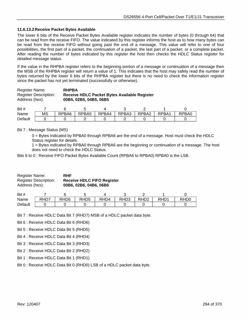
DS26556 4-Port Cell/Packet Over T1/E1/J1 Transceiver
Rev: 120407 294 of 370
11.6.13.2 Receive Packet Bytes Available The lower 6 bits of the Receive Packet Bytes Available register indicates the number of bytes (0 through 64) that can be read from the receive FIFO. The value indicated by this register informs the host as to how many bytes can be read from the receive FIFO without going past the end of a message. This value will refer to one of four possibilities, the first part of a packet, the continuation of a packet, the last part of a packet, or a complete packet. After reading the number of bytes indicated by this register the host then checks the HDLC Status register for detailed message status.
If the value in the RHPBA register refers to the beginning portion of a message or continuation of a message then the MSB of the RHPBA register will return a value of 1. This indicates that the host may safely read the number of bytes returned by the lower 6 bits of the RHPBA register but there is no need to check the information register since the packet has not yet terminated (successfully or otherwise). Register Name: RHPBA Register Description: Receive HDLC Packet Bytes Available Register Address (hex): 00B5, 02B5, 04B5, 06B5 Bit # 7 6 5 4 3 2 1 0 Name MS RPBA6 RPBA5 RPBA4 RPBA3 RPBA2 RPBA1 RPBA0 Default 0 0 0 0 0 0 0 0 Bit 7 : Message Status (MS)
0 = Bytes indicated by RPBA0 through RPBA6 are the end of a message. Host must check the HDLC Status register for details. 1 = Bytes indicated by RPBA0 through RPBA6 are the beginning or continuation of a message. The host does not need to check the HDLC Status.
Bits 6 to 0 : Receive FIFO Packet Bytes Available Count (RPBA6 to RPBA0) RPBA0 is the LSB.
Register Name: RHF Register Description: Receive HDLC FIFO Register Address (hex): 00B6, 02B6, 04B6, 06B6 Bit # 7 6 5 4 3 2 1 0 Name RHD7 RHD6 RHD5 RHD4 RHD3 RHD2 RHD1 RHD0 Default 0 0 0 0 0 0 0 0 Bit 7 : Receive HDLC Data Bit 7 (RHD7) MSB of a HDLC packet data byte.
Bit 6 : Receive HDLC Data Bit 6 (RHD6)
Bit 5 : Receive HDLC Data Bit 5 (RHD5)
Bit 4 : Receive HDLC Data Bit 4 (RHD4)
Bit 3 : Receive HDLC Data Bit 3 (RHD3)
Bit 2 : Receive HDLC Data Bit 2 (RHD2)
Bit 1 : Receive HDLC Data Bit 1 (RHD1)
Bit 0 : Receive HDLC Data Bit 0 (RHD0) LSB of a HDLC packet data byte.
DS26556 4-Port Cell/Packet Over T1/E1/J1 Transceiver
Rev: 120407 295 of 370
11.6.13.3 HDLC Status and Information RRTS5 and RLS5 provide status information for the receive HDLC controller. When a particular event has occurred (or is occurring), the appropriate bit in one of these registers will be set to a one. With the latched bits, when an event occurs and a bit is set to a one, it will remain set until the user reads that bit. The bit will be cleared when it is read and it will not be set again until the event has occurred again. The real-time bits report the current instantaneous conditions that are occurring and the history of these bits is not latched.
Like the other latched status registers, the user will follow a read of the status bit with a write. The byte written to the register will inform the device which of the latched bits the user wishes to clear (the real time bits are not affected by writing to the status register). The user will write a byte to one of these registers, with a one in the bit positions he or she wishes to clear and a zero in the bit positions he or she does not wish to clear.
The HDLC status register RLS5 has the ability to initiate a hardware interrupt via the INT output signal. Each of the events in this register can be either masked or unmasked from the interrupt pin via the receive HDLC Interrupt Mask Register (RIM5). Interrupts will force the INT signal low when the event occurs. The INT pin will be allowed to return high (if no other interrupts are present) when the user reads the event bit that caused the interrupt to occur.
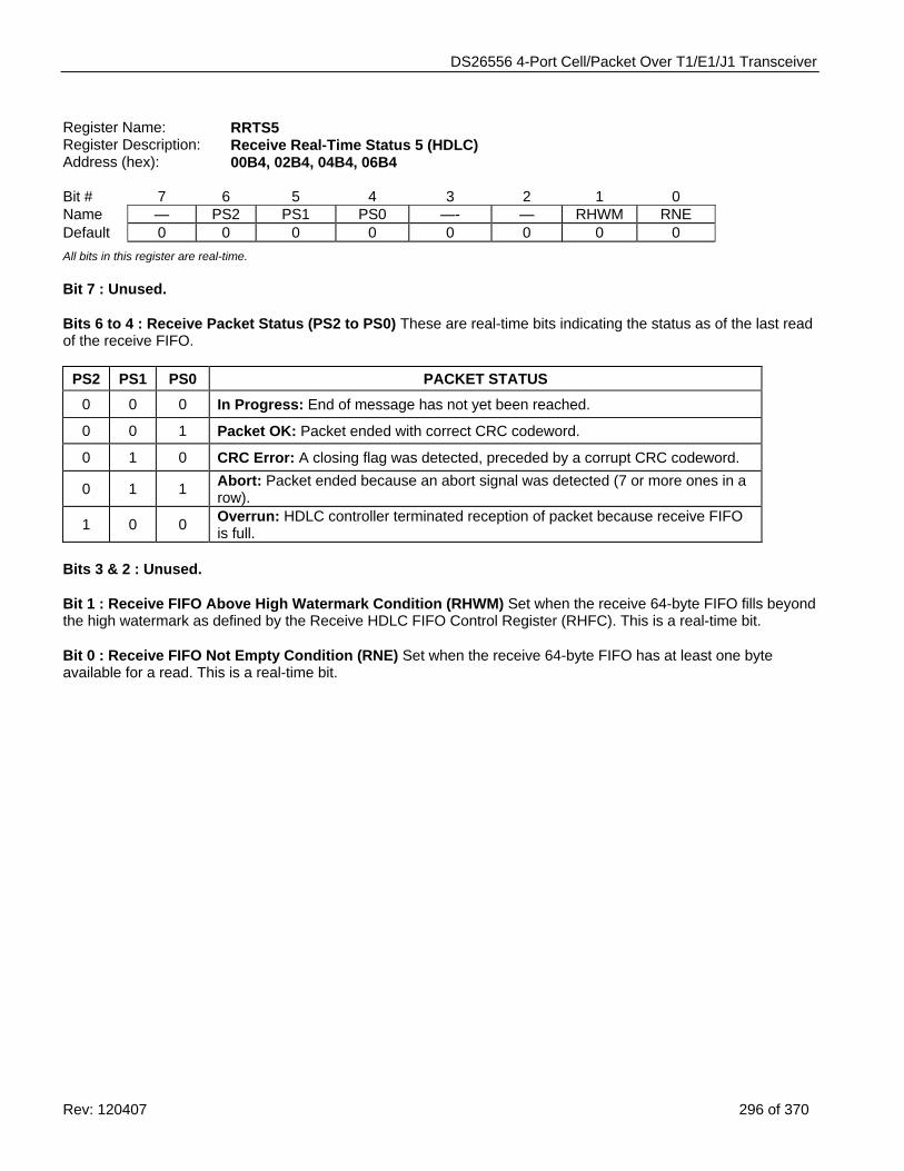
DS26556 4-Port Cell/Packet Over T1/E1/J1 Transceiver
Rev: 120407 296 of 370
Register Name: RRTS5 Register Description: Receive Real-Time Status 5 (HDLC) Address (hex): 00B4, 02B4, 04B4, 06B4 Bit # 7 6 5 4 3 2 1 0 Name — PS2 PS1 PS0 —- — RHWM RNE Default 0 0 0 0 0 0 0 0 All bits in this register are real-time. Bit 7 : Unused. Bits 6 to 4 : Receive Packet Status (PS2 to PS0) These are real-time bits indicating the status as of the last read of the receive FIFO.
PS2 PS1 PS0 PACKET STATUS 0 0 0 In Progress: End of message has not yet been reached.
0 0 1 Packet OK: Packet ended with correct CRC codeword.
0 1 0 CRC Error: A closing flag was detected, preceded by a corrupt CRC codeword.
0 1 1 Abort: Packet ended because an abort signal was detected (7 or more ones in a row).
1 0 0 Overrun: HDLC controller terminated reception of packet because receive FIFO is full.
Bits 3 & 2 : Unused. Bit 1 : Receive FIFO Above High Watermark Condition (RHWM) Set when the receive 64-byte FIFO fills beyond the high watermark as defined by the Receive HDLC FIFO Control Register (RHFC). This is a real-time bit. Bit 0 : Receive FIFO Not Empty Condition (RNE) Set when the receive 64-byte FIFO has at least one byte available for a read. This is a real-time bit.
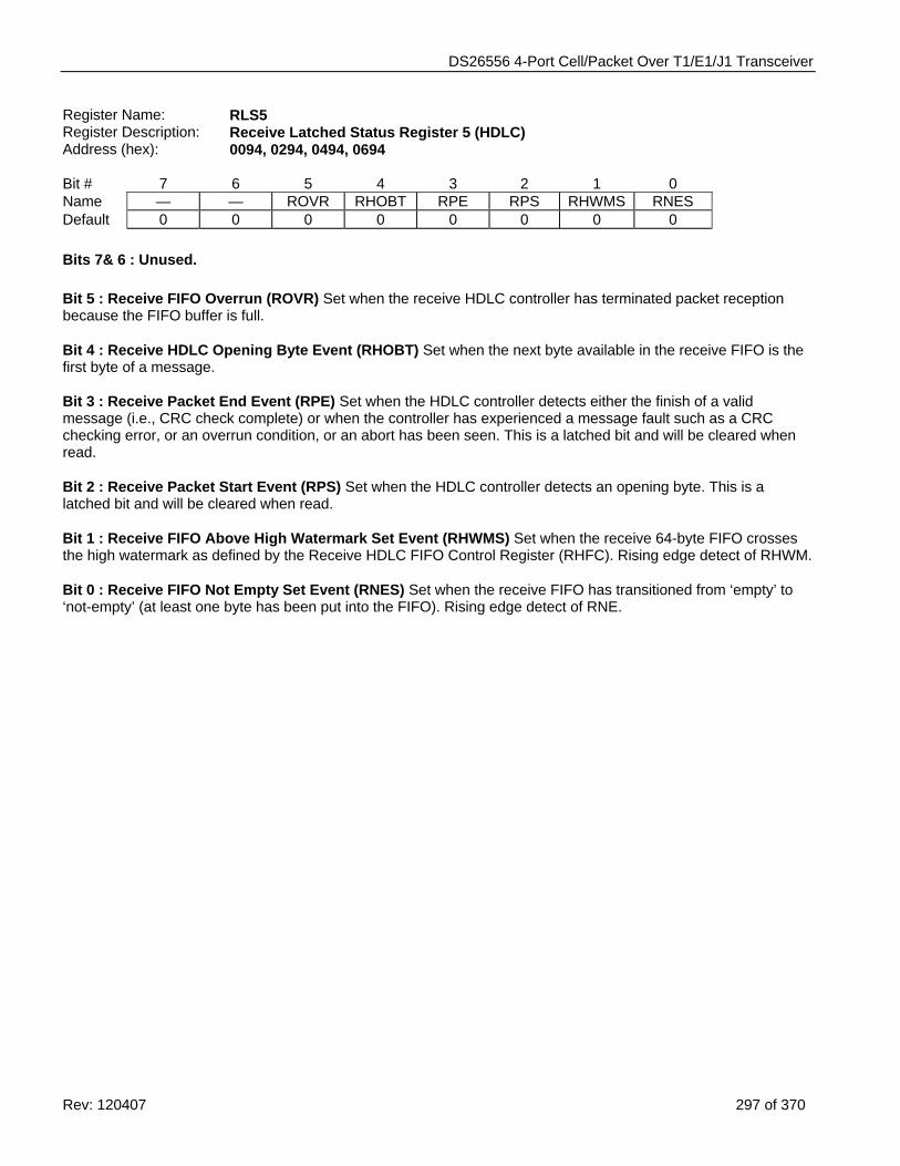
DS26556 4-Port Cell/Packet Over T1/E1/J1 Transceiver
Rev: 120407 297 of 370
Register Name: RLS5 Register Description: Receive Latched Status Register 5 (HDLC) Address (hex): 0094, 0294, 0494, 0694 Bit # 7 6 5 4 3 2 1 0 Name — — ROVR RHOBT RPE RPS RHWMS RNES Default 0 0 0 0 0 0 0 0 Bits 7& 6 : Unused. Bit 5 : Receive FIFO Overrun (ROVR) Set when the receive HDLC controller has terminated packet reception because the FIFO buffer is full. Bit 4 : Receive HDLC Opening Byte Event (RHOBT) Set when the next byte available in the receive FIFO is the first byte of a message. Bit 3 : Receive Packet End Event (RPE) Set when the HDLC controller detects either the finish of a valid message (i.e., CRC check complete) or when the controller has experienced a message fault such as a CRC checking error, or an overrun condition, or an abort has been seen. This is a latched bit and will be cleared when read. Bit 2 : Receive Packet Start Event (RPS) Set when the HDLC controller detects an opening byte. This is a latched bit and will be cleared when read. Bit 1 : Receive FIFO Above High Watermark Set Event (RHWMS) Set when the receive 64-byte FIFO crosses the high watermark as defined by the Receive HDLC FIFO Control Register (RHFC). Rising edge detect of RHWM. Bit 0 : Receive FIFO Not Empty Set Event (RNES) Set when the receive FIFO has transitioned from ‘empty’ to ‘not-empty’ (at least one byte has been put into the FIFO). Rising edge detect of RNE.
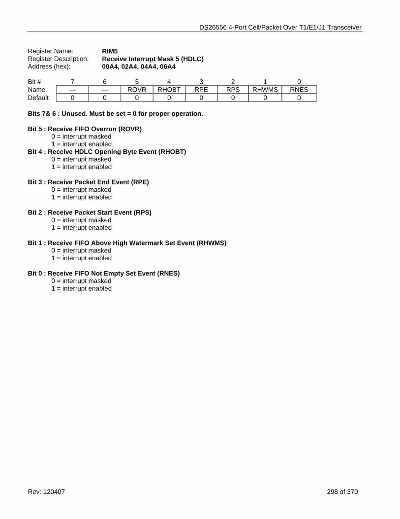
DS26556 4-Port Cell/Packet Over T1/E1/J1 Transceiver
Rev: 120407 298 of 370
Register Name: RIM5 Register Description: Receive Interrupt Mask 5 (HDLC) Address (hex): 00A4, 02A4, 04A4, 06A4 Bit # 7 6 5 4 3 2 1 0 Name — — ROVR RHOBT RPE RPS RHWMS RNES Default 0 0 0 0 0 0 0 0 Bits 7& 6 : Unused. Must be set = 0 for proper operation. Bit 5 : Receive FIFO Overrun (ROVR)
0 = interrupt masked 1 = interrupt enabled
Bit 4 : Receive HDLC Opening Byte Event (RHOBT) 0 = interrupt masked 1 = interrupt enabled
Bit 3 : Receive Packet End Event (RPE) 0 = interrupt masked 1 = interrupt enabled
Bit 2 : Receive Packet Start Event (RPS)
0 = interrupt masked 1 = interrupt enabled
Bit 1 : Receive FIFO Above High Watermark Set Event (RHWMS)
0 = interrupt masked 1 = interrupt enabled
Bit 0 : Receive FIFO Not Empty Set Event (RNES)
0 = interrupt masked 1 = interrupt enabled
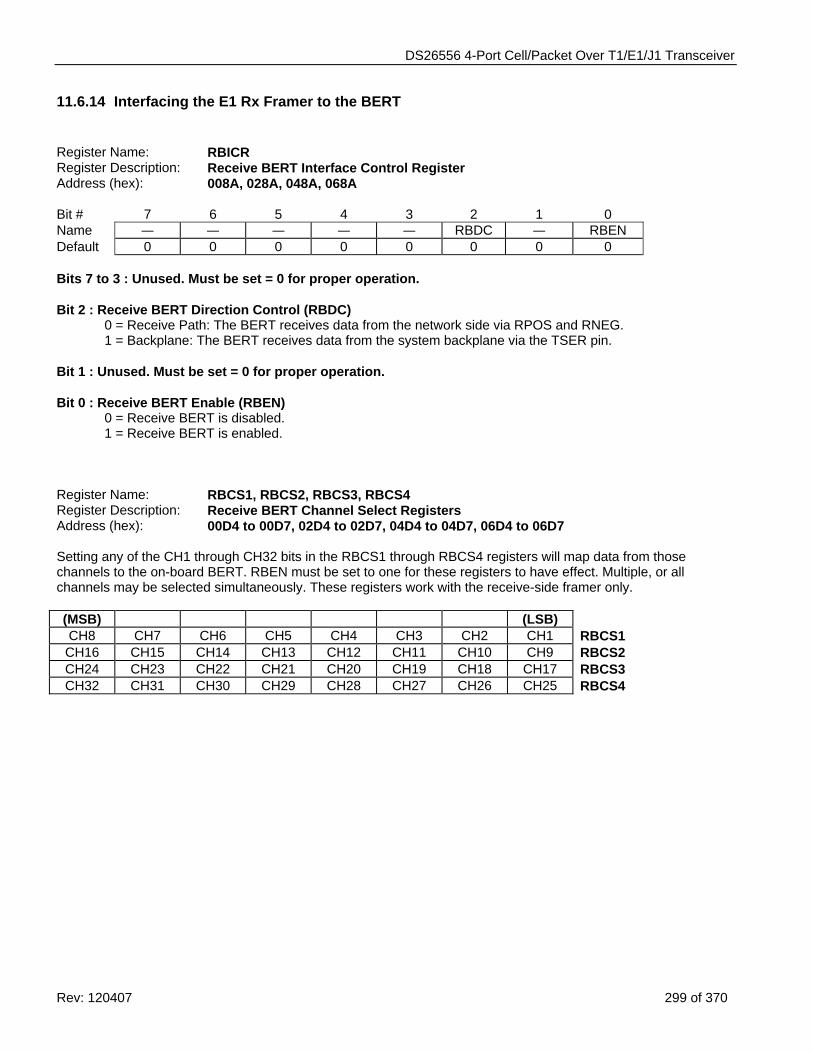
DS26556 4-Port Cell/Packet Over T1/E1/J1 Transceiver
Rev: 120407 299 of 370
11.6.14 Interfacing the E1 Rx Framer to the BERT Register Name: RBICR Register Description: Receive BERT Interface Control Register Address (hex): 008A, 028A, 048A, 068A Bit # 7 6 5 4 3 2 1 0 Name — — — — — RBDC — RBEN Default 0 0 0 0 0 0 0 0 Bits 7 to 3 : Unused. Must be set = 0 for proper operation. Bit 2 : Receive BERT Direction Control (RBDC) 0 = Receive Path: The BERT receives data from the network side via RPOS and RNEG.
1 = Backplane: The BERT receives data from the system backplane via the TSER pin. Bit 1 : Unused. Must be set = 0 for proper operation. Bit 0 : Receive BERT Enable (RBEN) 0 = Receive BERT is disabled.
1 = Receive BERT is enabled. Register Name: RBCS1, RBCS2, RBCS3, RBCS4 Register Description: Receive BERT Channel Select Registers Address (hex): 00D4 to 00D7, 02D4 to 02D7, 04D4 to 04D7, 06D4 to 06D7 Setting any of the CH1 through CH32 bits in the RBCS1 through RBCS4 registers will map data from those channels to the on-board BERT. RBEN must be set to one for these registers to have effect. Multiple, or all channels may be selected simultaneously. These registers work with the receive-side framer only. (MSB) (LSB) CH8 CH7 CH6 CH5 CH4 CH3 CH2 CH1 RBCS1 CH16 CH15 CH14 CH13 CH12 CH11 CH10 CH9 RBCS2 CH24 CH23 CH22 CH21 CH20 CH19 CH18 CH17 RBCS3 CH32 CH31 CH30 CH29 CH28 CH27 CH26 CH25 RBCS4
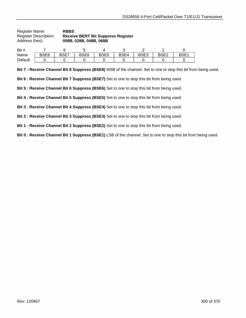
DS26556 4-Port Cell/Packet Over T1/E1/J1 Transceiver
Rev: 120407 300 of 370
Register Name: RBBS Register Description: Receive BERT Bit Suppress Register Address (hex): 008B, 028B, 048B, 068B Bit # 7 6 5 4 3 2 1 0 Name BSE8 BSE7 BSE6 BSE5 BSE4 BSE3 BSE2 BSE1 Default 0 0 0 0 0 0 0 0 Bit 7 : Receive Channel Bit 8 Suppress (BSE8) MSB of the channel. Set to one to stop this bit from being used. Bit 6 : Receive Channel Bit 7 Suppress (BSE7) Set to one to stop this bit from being used. Bit 5 : Receive Channel Bit 6 Suppress (BSE6) Set to one to stop this bit from being used. Bit 4 : Receive Channel Bit 5 Suppress (BSE5) Set to one to stop this bit from being used. Bit 3 : Receive Channel Bit 4 Suppress (BSE4) Set to one to stop this bit from being used. Bit 2 : Receive Channel Bit 3 Suppress (BSE3) Set to one to stop this bit from being used. Bit 1 : Receive Channel Bit 2 Suppress (BSE2) Set to one to stop this bit from being used. Bit 0 : Receive Channel Bit 1 Suppress (BSE1) LSB of the channel. Set to one to stop this bit from being used.
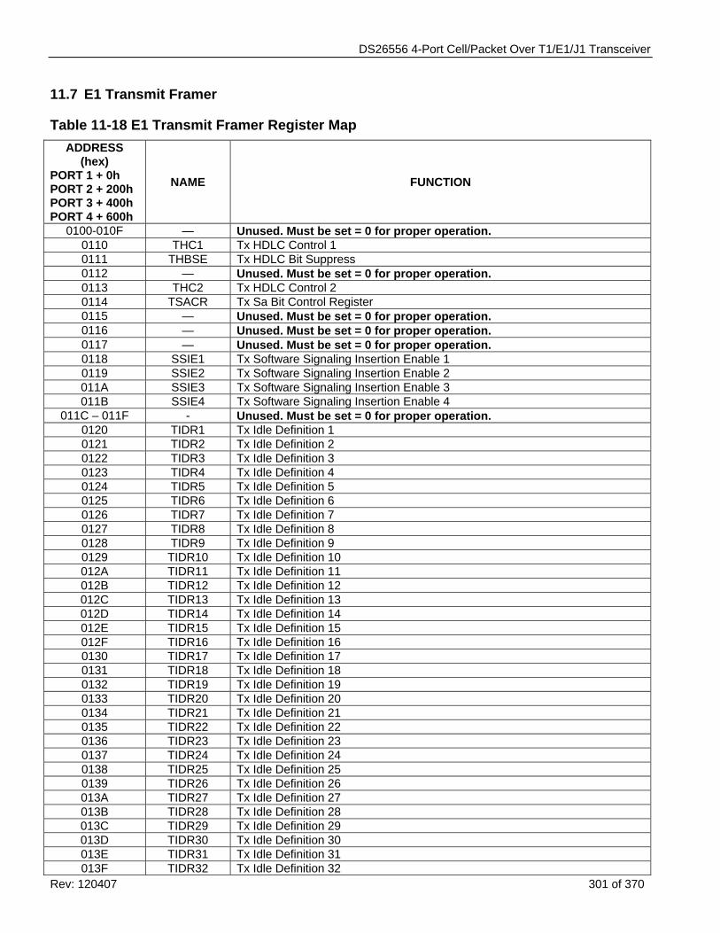
DS26556 4-Port Cell/Packet Over T1/E1/J1 Transceiver
Rev: 120407 301 of 370
11.7 E1 Transmit Framer
Table 11-18 E1 Transmit Framer Register Map ADDRESS
(hex) PORT 1 + 0h PORT 2 + 200h PORT 3 + 400h PORT 4 + 600h
NAME FUNCTION
0100-010F — Unused. Must be set = 0 for proper operation. 0110 THC1 Tx HDLC Control 1 0111 THBSE Tx HDLC Bit Suppress 0112 — Unused. Must be set = 0 for proper operation. 0113 THC2 Tx HDLC Control 2 0114 TSACR Tx Sa Bit Control Register 0115 — Unused. Must be set = 0 for proper operation. 0116 — Unused. Must be set = 0 for proper operation. 0117 — Unused. Must be set = 0 for proper operation. 0118 SSIE1 Tx Software Signaling Insertion Enable 1 0119 SSIE2 Tx Software Signaling Insertion Enable 2 011A SSIE3 Tx Software Signaling Insertion Enable 3 011B SSIE4 Tx Software Signaling Insertion Enable 4
011C – 011F - Unused. Must be set = 0 for proper operation. 0120 TIDR1 Tx Idle Definition 1 0121 TIDR2 Tx Idle Definition 2 0122 TIDR3 Tx Idle Definition 3 0123 TIDR4 Tx Idle Definition 4 0124 TIDR5 Tx Idle Definition 5 0125 TIDR6 Tx Idle Definition 6 0126 TIDR7 Tx Idle Definition 7 0127 TIDR8 Tx Idle Definition 8 0128 TIDR9 Tx Idle Definition 9 0129 TIDR10 Tx Idle Definition 10 012A TIDR11 Tx Idle Definition 11 012B TIDR12 Tx Idle Definition 12 012C TIDR13 Tx Idle Definition 13 012D TIDR14 Tx Idle Definition 14 012E TIDR15 Tx Idle Definition 15 012F TIDR16 Tx Idle Definition 16 0130 TIDR17 Tx Idle Definition 17 0131 TIDR18 Tx Idle Definition 18 0132 TIDR19 Tx Idle Definition 19 0133 TIDR20 Tx Idle Definition 20 0134 TIDR21 Tx Idle Definition 21 0135 TIDR22 Tx Idle Definition 22 0136 TIDR23 Tx Idle Definition 23 0137 TIDR24 Tx Idle Definition 24 0138 TIDR25 Tx Idle Definition 25 0139 TIDR26 Tx Idle Definition 26 013A TIDR27 Tx Idle Definition 27 013B TIDR28 Tx Idle Definition 28 013C TIDR29 Tx Idle Definition 29 013D TIDR30 Tx Idle Definition 30 013E TIDR31 Tx Idle Definition 31 013F TIDR32 Tx Idle Definition 32
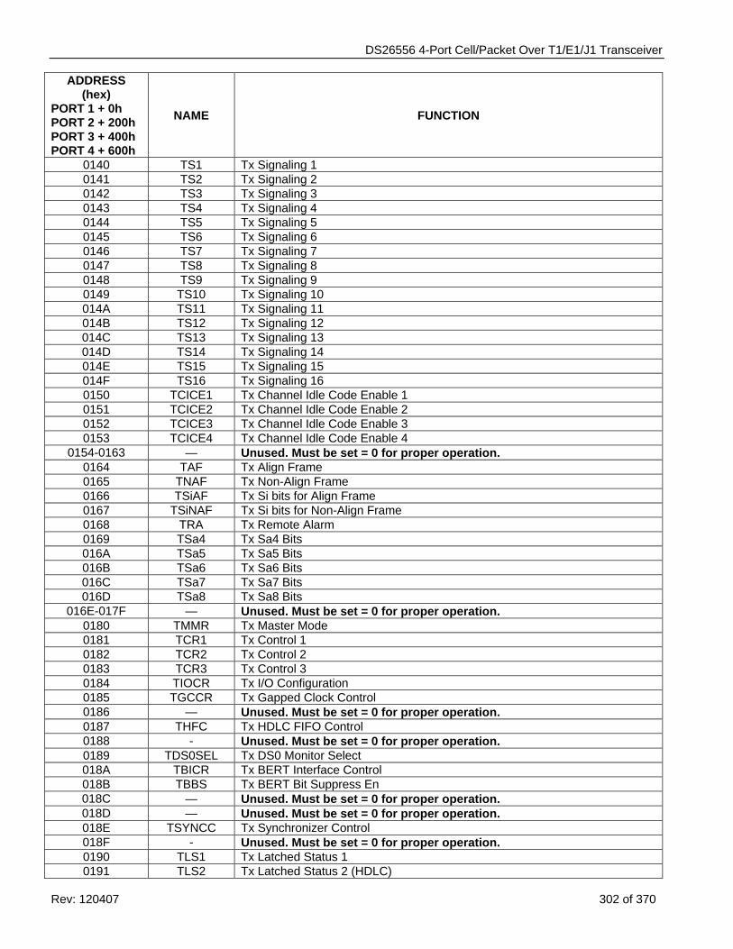
DS26556 4-Port Cell/Packet Over T1/E1/J1 Transceiver
Rev: 120407 302 of 370
ADDRESS (hex)
PORT 1 + 0h PORT 2 + 200h PORT 3 + 400h PORT 4 + 600h
NAME FUNCTION
0140 TS1 Tx Signaling 1 0141 TS2 Tx Signaling 2 0142 TS3 Tx Signaling 3 0143 TS4 Tx Signaling 4 0144 TS5 Tx Signaling 5 0145 TS6 Tx Signaling 6 0146 TS7 Tx Signaling 7 0147 TS8 Tx Signaling 8 0148 TS9 Tx Signaling 9 0149 TS10 Tx Signaling 10 014A TS11 Tx Signaling 11 014B TS12 Tx Signaling 12 014C TS13 Tx Signaling 13 014D TS14 Tx Signaling 14 014E TS15 Tx Signaling 15 014F TS16 Tx Signaling 16 0150 TCICE1 Tx Channel Idle Code Enable 1 0151 TCICE2 Tx Channel Idle Code Enable 2 0152 TCICE3 Tx Channel Idle Code Enable 3 0153 TCICE4 Tx Channel Idle Code Enable 4
0154-0163 — Unused. Must be set = 0 for proper operation. 0164 TAF Tx Align Frame 0165 TNAF Tx Non-Align Frame 0166 TSiAF Tx Si bits for Align Frame 0167 TSiNAF Tx Si bits for Non-Align Frame 0168 TRA Tx Remote Alarm 0169 TSa4 Tx Sa4 Bits 016A TSa5 Tx Sa5 Bits 016B TSa6 Tx Sa6 Bits 016C TSa7 Tx Sa7 Bits 016D TSa8 Tx Sa8 Bits
016E-017F — Unused. Must be set = 0 for proper operation. 0180 TMMR Tx Master Mode 0181 TCR1 Tx Control 1 0182 TCR2 Tx Control 2 0183 TCR3 Tx Control 3 0184 TIOCR Tx I/O Configuration 0185 TGCCR Tx Gapped Clock Control 0186 — Unused. Must be set = 0 for proper operation. 0187 THFC Tx HDLC FIFO Control 0188 - Unused. Must be set = 0 for proper operation. 0189 TDS0SEL Tx DS0 Monitor Select 018A TBICR Tx BERT Interface Control 018B TBBS Tx BERT Bit Suppress En 018C — Unused. Must be set = 0 for proper operation. 018D — Unused. Must be set = 0 for proper operation. 018E TSYNCC Tx Synchronizer Control 018F - Unused. Must be set = 0 for proper operation. 0190 TLS1 Tx Latched Status 1 0191 TLS2 Tx Latched Status 2 (HDLC)
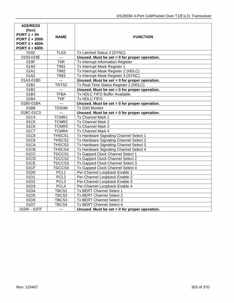
DS26556 4-Port Cell/Packet Over T1/E1/J1 Transceiver
Rev: 120407 303 of 370
ADDRESS (hex)
PORT 1 + 0h PORT 2 + 200h PORT 3 + 400h PORT 4 + 600h
NAME FUNCTION
0192 TLS3 Tx Latched Status 3 (SYNC) 0193-019E — Unused. Must be set = 0 for proper operation.
019F TIIR Tx Interrupt Information Register 01A0 TIM1 Tx Interrupt Mask Register 1 01A1 TIM2 Tx Interrupt Mask Register 2 (HDLC) 01A2 TIM3 Tx Interrupt Mask Register 3 (SYNC)
01A3-01B0 — Unused. Must be set = 0 for proper operation. 01B1 TRTS2 Tx Real-Time Status Register 2 (HDLC) 01B2 — Unused. Must be set = 0 for proper operation. 01B3 TFBA Tx HDLC FIFO Buffer Available 01B4 THF Tx HDLC FIFO
01B5-01BA — Unused. Must be set = 0 for proper operation. 01BB TDS0M Tx DS0 Monitor
01BC-01C3 — Unused. Must be set = 0 for proper operation. 01C4 TCMR1 Tx Channel Mark 1 01C5 TCMR2 Tx Channel Mark 2 01C6 TCMR3 Tx Channel Mark 3 01C7 TCMR4 Tx Channel Mark 4 01C8 THSCS1 Tx Hardware Signaling Channel Select 1 01C9 THSCS2 Tx Hardware Signaling Channel Select 2 01CA THSCS3 Tx Hardware Signaling Channel Select 3 01CB THSCS4 Tx Hardware Signaling Channel Select 4 01CC TGCCS1 Tx Gapped Clock Channel Select 1 01CD TGCCS2 Tx Gapped Clock Channel Select 2 01CE TGCCS3 Tx Gapped Clock Channel Select 3 01CF TGCCS4 Tx Gapped Clock Channel Select 4 01D0 PCL1 Per-Channel Loopback Enable 1 01D1 PCL2 Per-Channel Loopback Enable 2 01D2 PCL3 Per-Channel Loopback Enable 3 01D3 PCL4 Per-Channel Loopback Enable 4 01D4 TBCS1 Tx BERT Channel Select 1 01D5 TBCS2 Tx BERT Channel Select 2 01D6 TBCS3 Tx BERT Channel Select 3 01D7 TBCS4 Tx BERT Channel Select 4
01D8 – 01FF — Unused. Must be set = 0 for proper operation.
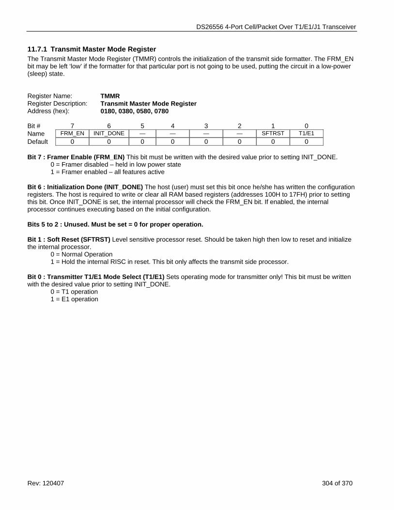
DS26556 4-Port Cell/Packet Over T1/E1/J1 Transceiver
Rev: 120407 304 of 370
11.7.1 Transmit Master Mode Register The Transmit Master Mode Register (TMMR) controls the initialization of the transmit side formatter. The FRM_EN bit may be left ‘low’ if the formatter for that particular port is not going to be used, putting the circuit in a low-power (sleep) state. Register Name: TMMR Register Description: Transmit Master Mode Register Address (hex): 0180, 0380, 0580, 0780 Bit # 7 6 5 4 3 2 1 0 Name FRM_EN INIT_DONE — — — — SFTRST T1/E1 Default 0 0 0 0 0 0 0 0 Bit 7 : Framer Enable (FRM_EN) This bit must be written with the desired value prior to setting INIT_DONE. 0 = Framer disabled – held in low power state 1 = Framer enabled – all features active Bit 6 : Initialization Done (INIT_DONE) The host (user) must set this bit once he/she has written the configuration registers. The host is required to write or clear all RAM based registers (addresses 100H to 17FH) prior to setting this bit. Once INIT_DONE is set, the internal processor will check the FRM_EN bit. If enabled, the internal processor continues executing based on the initial configuration. Bits 5 to 2 : Unused. Must be set = 0 for proper operation. Bit 1 : Soft Reset (SFTRST) Level sensitive processor reset. Should be taken high then low to reset and initialize the internal processor.
0 = Normal Operation 1 = Hold the internal RISC in reset. This bit only affects the transmit side processor.
Bit 0 : Transmitter T1/E1 Mode Select (T1/E1) Sets operating mode for transmitter only! This bit must be written with the desired value prior to setting INIT_DONE.
0 = T1 operation 1 = E1 operation
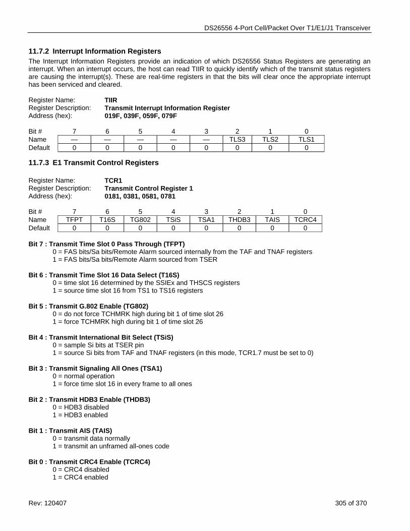
DS26556 4-Port Cell/Packet Over T1/E1/J1 Transceiver
Rev: 120407 305 of 370
11.7.2 Interrupt Information Registers The Interrupt Information Registers provide an indication of which DS26556 Status Registers are generating an interrupt. When an interrupt occurs, the host can read TIIR to quickly identify which of the transmit status registers are causing the interrupt(s). These are real-time registers in that the bits will clear once the appropriate interrupt has been serviced and cleared.
Register Name: TIIR Register Description: Transmit Interrupt Information Register Address (hex): 019F, 039F, 059F, 079F Bit # 7 6 5 4 3 2 1 0 Name — — — — — TLS3 TLS2 TLS1 Default 0 0 0 0 0 0 0 0
11.7.3 E1 Transmit Control Registers
Register Name: TCR1 Register Description: Transmit Control Register 1 Address (hex): 0181, 0381, 0581, 0781 Bit # 7 6 5 4 3 2 1 0 Name TFPT T16S TG802 TSiS TSA1 THDB3 TAIS TCRC4 Default 0 0 0 0 0 0 0 0 Bit 7 : Transmit Time Slot 0 Pass Through (TFPT)
0 = FAS bits/Sa bits/Remote Alarm sourced internally from the TAF and TNAF registers 1 = FAS bits/Sa bits/Remote Alarm sourced from TSER
Bit 6 : Transmit Time Slot 16 Data Select (T16S)
0 = time slot 16 determined by the SSIEx and THSCS registers 1 = source time slot 16 from TS1 to TS16 registers
Bit 5 : Transmit G.802 Enable (TG802)
0 = do not force TCHMRK high during bit 1 of time slot 26 1 = force TCHMRK high during bit 1 of time slot 26
Bit 4 : Transmit International Bit Select (TSiS)
0 = sample Si bits at TSER pin 1 = source Si bits from TAF and TNAF registers (in this mode, TCR1.7 must be set to 0)
Bit 3 : Transmit Signaling All Ones (TSA1) 0 = normal operation 1 = force time slot 16 in every frame to all ones
Bit 2 : Transmit HDB3 Enable (THDB3)
0 = HDB3 disabled 1 = HDB3 enabled
Bit 1 : Transmit AIS (TAIS)
0 = transmit data normally 1 = transmit an unframed all-ones code
Bit 0 : Transmit CRC4 Enable (TCRC4)
0 = CRC4 disabled 1 = CRC4 enabled
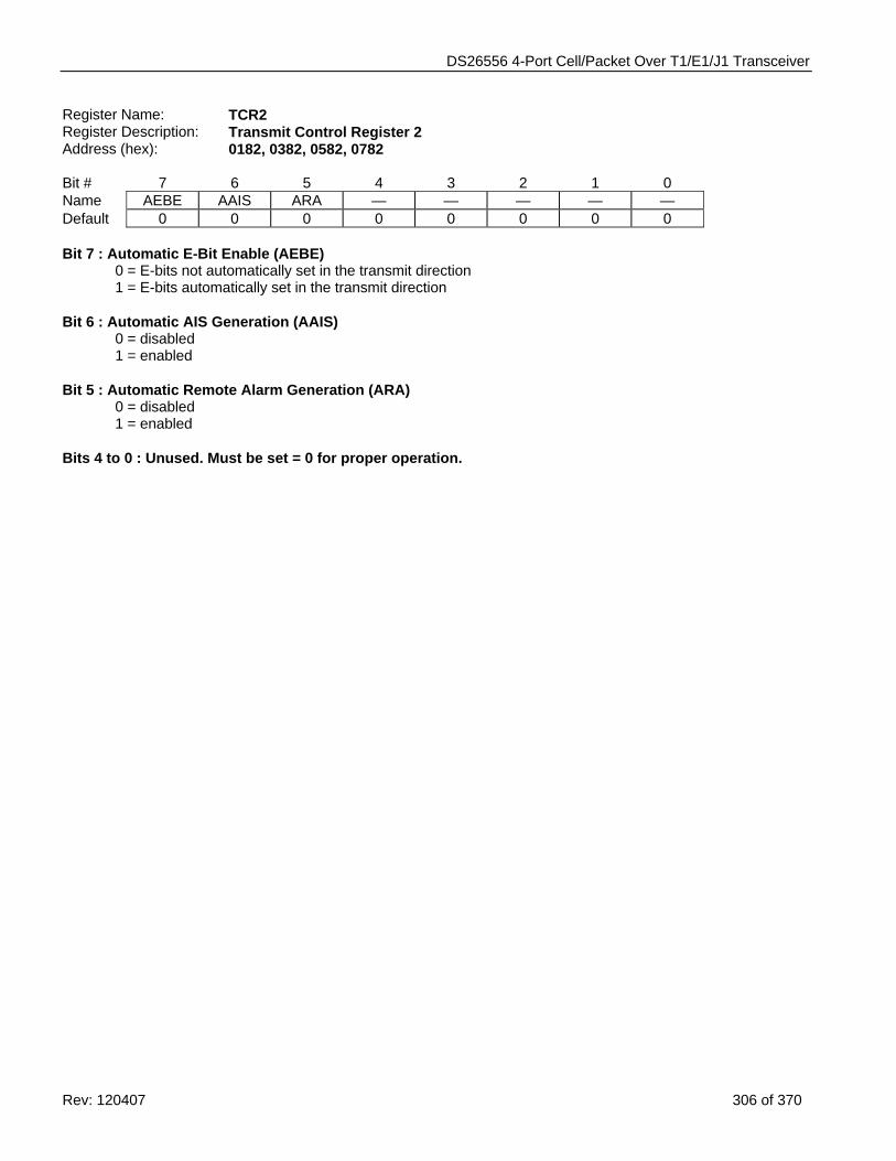
DS26556 4-Port Cell/Packet Over T1/E1/J1 Transceiver
Rev: 120407 306 of 370
Register Name: TCR2 Register Description: Transmit Control Register 2 Address (hex): 0182, 0382, 0582, 0782 Bit # 7 6 5 4 3 2 1 0 Name AEBE AAIS ARA — — — — — Default 0 0 0 0 0 0 0 0 Bit 7 : Automatic E-Bit Enable (AEBE)
0 = E-bits not automatically set in the transmit direction 1 = E-bits automatically set in the transmit direction
Bit 6 : Automatic AIS Generation (AAIS)
0 = disabled 1 = enabled
Bit 5 : Automatic Remote Alarm Generation (ARA)
0 = disabled 1 = enabled
Bits 4 to 0 : Unused. Must be set = 0 for proper operation.
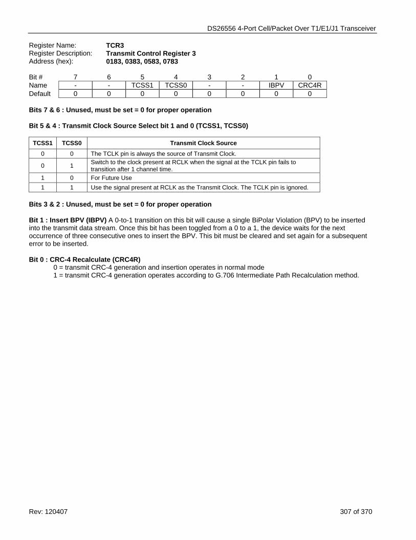
DS26556 4-Port Cell/Packet Over T1/E1/J1 Transceiver
Rev: 120407 307 of 370
Register Name: TCR3 Register Description: Transmit Control Register 3 Address (hex): 0183, 0383, 0583, 0783 Bit # 7 6 5 4 3 2 1 0 Name - - TCSS1 TCSS0 - - IBPV CRC4R Default 0 0 0 0 0 0 0 0 Bits 7 & 6 : Unused, must be set = 0 for proper operation Bit 5 & 4 : Transmit Clock Source Select bit 1 and 0 (TCSS1, TCSS0)
TCSS1 TCSS0 Transmit Clock Source
0 0 The TCLK pin is always the source of Transmit Clock.
0 1 Switch to the clock present at RCLK when the signal at the TCLK pin fails to transition after 1 channel time.
1 0 For Future Use 1 1 Use the signal present at RCLK as the Transmit Clock. The TCLK pin is ignored.
Bits 3 & 2 : Unused, must be set = 0 for proper operation Bit 1 : Insert BPV (IBPV) A 0-to-1 transition on this bit will cause a single BiPolar Violation (BPV) to be inserted into the transmit data stream. Once this bit has been toggled from a 0 to a 1, the device waits for the next occurrence of three consecutive ones to insert the BPV. This bit must be cleared and set again for a subsequent error to be inserted. Bit 0 : CRC-4 Recalculate (CRC4R) 0 = transmit CRC-4 generation and insertion operates in normal mode
1 = transmit CRC-4 generation operates according to G.706 Intermediate Path Recalculation method.
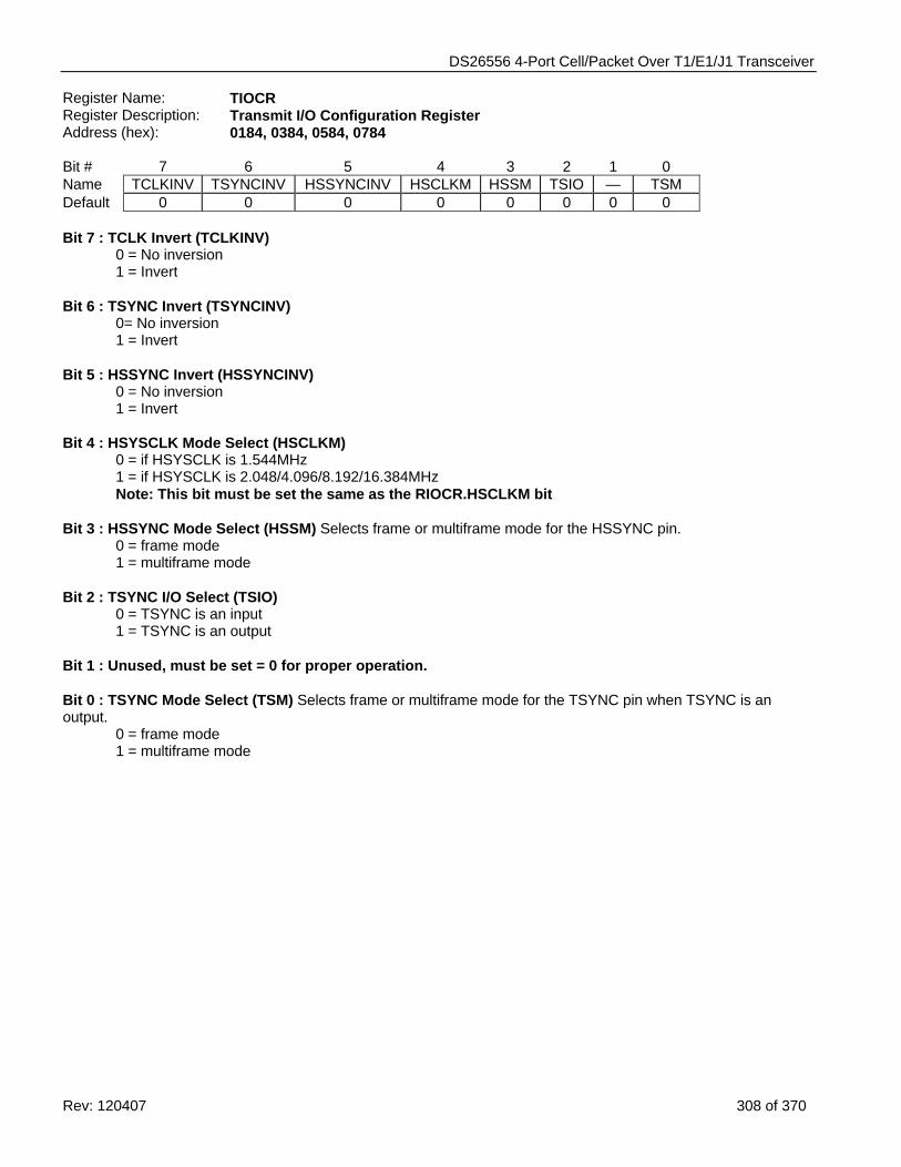
DS26556 4-Port Cell/Packet Over T1/E1/J1 Transceiver
Rev: 120407 308 of 370
Register Name: TIOCR Register Description: Transmit I/O Configuration Register Address (hex): 0184, 0384, 0584, 0784 Bit # 7 6 5 4 3 2 1 0 Name TCLKINV TSYNCINV HSSYNCINV HSCLKM HSSM TSIO — TSM Default 0 0 0 0 0 0 0 0 Bit 7 : TCLK Invert (TCLKINV)
0 = No inversion 1 = Invert
Bit 6 : TSYNC Invert (TSYNCINV)
0= No inversion 1 = Invert
Bit 5 : HSSYNC Invert (HSSYNCINV)
0 = No inversion 1 = Invert
Bit 4 : HSYSCLK Mode Select (HSCLKM)
0 = if HSYSCLK is 1.544MHz 1 = if HSYSCLK is 2.048/4.096/8.192/16.384MHz
Note: This bit must be set the same as the RIOCR.HSCLKM bit Bit 3 : HSSYNC Mode Select (HSSM) Selects frame or multiframe mode for the HSSYNC pin.
0 = frame mode 1 = multiframe mode
Bit 2 : TSYNC I/O Select (TSIO)
0 = TSYNC is an input 1 = TSYNC is an output
Bit 1 : Unused, must be set = 0 for proper operation. Bit 0 : TSYNC Mode Select (TSM) Selects frame or multiframe mode for the TSYNC pin when TSYNC is an output.
0 = frame mode 1 = multiframe mode
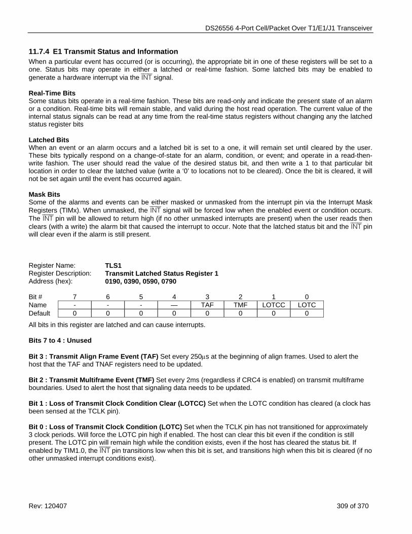
DS26556 4-Port Cell/Packet Over T1/E1/J1 Transceiver
Rev: 120407 309 of 370
11.7.4 E1 Transmit Status and Information When a particular event has occurred (or is occurring), the appropriate bit in one of these registers will be set to a one. Status bits may operate in either a latched or real-time fashion. Some latched bits may be enabled to generate a hardware interrupt via the INT signal. Real-Time Bits Some status bits operate in a real-time fashion. These bits are read-only and indicate the present state of an alarm or a condition. Real-time bits will remain stable, and valid during the host read operation. The current value of the internal status signals can be read at any time from the real-time status registers without changing any the latched status register bits Latched Bits When an event or an alarm occurs and a latched bit is set to a one, it will remain set until cleared by the user. These bits typically respond on a change-of-state for an alarm, condition, or event; and operate in a read-then-write fashion. The user should read the value of the desired status bit, and then write a 1 to that particular bit location in order to clear the latched value (write a ‘0’ to locations not to be cleared). Once the bit is cleared, it will not be set again until the event has occurred again. Mask Bits Some of the alarms and events can be either masked or unmasked from the interrupt pin via the Interrupt Mask Registers (TIMx). When unmasked, the INT signal will be forced low when the enabled event or condition occurs. The INT pin will be allowed to return high (if no other unmasked interrupts are present) when the user reads then clears (with a write) the alarm bit that caused the interrupt to occur. Note that the latched status bit and the INT pin will clear even if the alarm is still present.
Register Name: TLS1 Register Description: Transmit Latched Status Register 1 Address (hex): 0190, 0390, 0590, 0790 Bit # 7 6 5 4 3 2 1 0 Name - - - — TAF TMF LOTCC LOTC Default 0 0 0 0 0 0 0 0
All bits in this register are latched and can cause interrupts. Bits 7 to 4 : Unused Bit 3 : Transmit Align Frame Event (TAF) Set every 250μs at the beginning of align frames. Used to alert the host that the TAF and TNAF registers need to be updated. Bit 2 : Transmit Multiframe Event (TMF) Set every 2ms (regardless if CRC4 is enabled) on transmit multiframe boundaries. Used to alert the host that signaling data needs to be updated. Bit 1 : Loss of Transmit Clock Condition Clear (LOTCC) Set when the LOTC condition has cleared (a clock has been sensed at the TCLK pin). Bit 0 : Loss of Transmit Clock Condition (LOTC) Set when the TCLK pin has not transitioned for approximately 3 clock periods. Will force the LOTC pin high if enabled. The host can clear this bit even if the condition is still present. The LOTC pin will remain high while the condition exists, even if the host has cleared the status bit. If enabled by TIM1.0, the INT pin transitions low when this bit is set, and transitions high when this bit is cleared (if no other unmasked interrupt conditions exist).
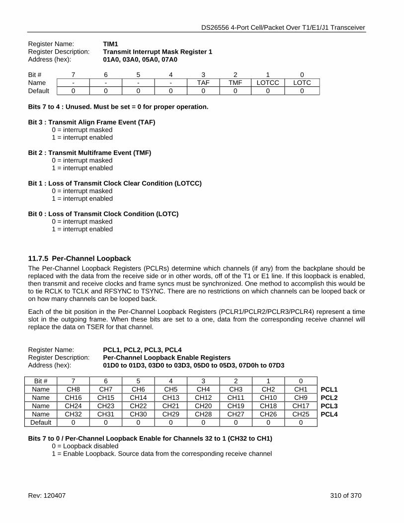
DS26556 4-Port Cell/Packet Over T1/E1/J1 Transceiver
Rev: 120407 310 of 370
Register Name: TIM1 Register Description: Transmit Interrupt Mask Register 1 Address (hex): 01A0, 03A0, 05A0, 07A0 Bit # 7 6 5 4 3 2 1 0 Name - - - - TAF TMF LOTCC LOTC Default 0 0 0 0 0 0 0 0 Bits 7 to 4 : Unused. Must be set = 0 for proper operation. Bit 3 : Transmit Align Frame Event (TAF)
0 = interrupt masked 1 = interrupt enabled
Bit 2 : Transmit Multiframe Event (TMF)
0 = interrupt masked 1 = interrupt enabled
Bit 1 : Loss of Transmit Clock Clear Condition (LOTCC)
0 = interrupt masked 1 = interrupt enabled
Bit 0 : Loss of Transmit Clock Condition (LOTC)
0 = interrupt masked 1 = interrupt enabled
11.7.5 Per-Channel Loopback The Per-Channel Loopback Registers (PCLRs) determine which channels (if any) from the backplane should be replaced with the data from the receive side or in other words, off of the T1 or E1 line. If this loopback is enabled, then transmit and receive clocks and frame syncs must be synchronized. One method to accomplish this would be to tie RCLK to TCLK and RFSYNC to TSYNC. There are no restrictions on which channels can be looped back or on how many channels can be looped back.
Each of the bit position in the Per-Channel Loopback Registers (PCLR1/PCLR2/PCLR3/PCLR4) represent a time slot in the outgoing frame. When these bits are set to a one, data from the corresponding receive channel will replace the data on TSER for that channel. Register Name: PCL1, PCL2, PCL3, PCL4 Register Description: Per-Channel Loopback Enable Registers Address (hex): 01D0 to 01D3, 03D0 to 03D3, 05D0 to 05D3, 07D0h to 07D3
Bit # 7 6 5 4 3 2 1 0 Name CH8 CH7 CH6 CH5 CH4 CH3 CH2 CH1 PCL1 Name CH16 CH15 CH14 CH13 CH12 CH11 CH10 CH9 PCL2 Name CH24 CH23 CH22 CH21 CH20 CH19 CH18 CH17 PCL3 Name CH32 CH31 CH30 CH29 CH28 CH27 CH26 CH25 PCL4 Default 0 0 0 0 0 0 0 0
Bits 7 to 0 / Per-Channel Loopback Enable for Channels 32 to 1 (CH32 to CH1)
0 = Loopback disabled 1 = Enable Loopback. Source data from the corresponding receive channel
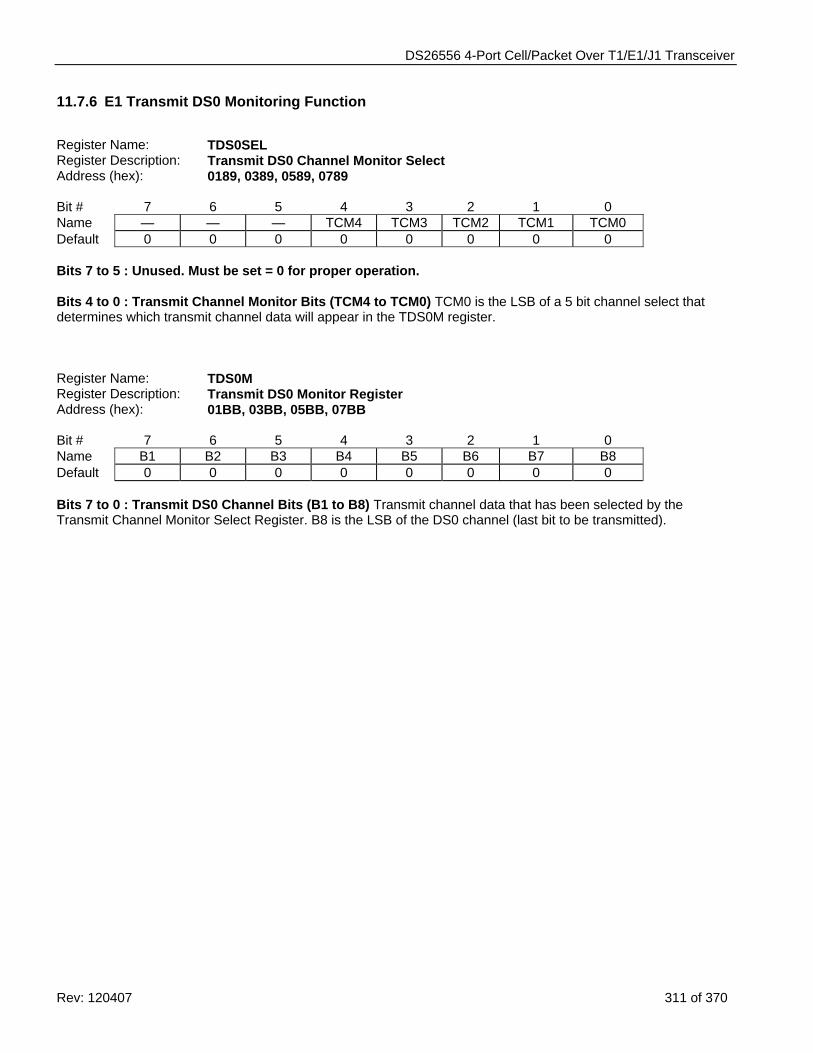
DS26556 4-Port Cell/Packet Over T1/E1/J1 Transceiver
Rev: 120407 311 of 370
11.7.6 E1 Transmit DS0 Monitoring Function Register Name: TDS0SEL Register Description: Transmit DS0 Channel Monitor Select Address (hex): 0189, 0389, 0589, 0789 Bit # 7 6 5 4 3 2 1 0 Name — — — TCM4 TCM3 TCM2 TCM1 TCM0 Default 0 0 0 0 0 0 0 0 Bits 7 to 5 : Unused. Must be set = 0 for proper operation. Bits 4 to 0 : Transmit Channel Monitor Bits (TCM4 to TCM0) TCM0 is the LSB of a 5 bit channel select that determines which transmit channel data will appear in the TDS0M register. Register Name: TDS0M Register Description: Transmit DS0 Monitor Register Address (hex): 01BB, 03BB, 05BB, 07BB Bit # 7 6 5 4 3 2 1 0 Name B1 B2 B3 B4 B5 B6 B7 B8 Default 0 0 0 0 0 0 0 0 Bits 7 to 0 : Transmit DS0 Channel Bits (B1 to B8) Transmit channel data that has been selected by the Transmit Channel Monitor Select Register. B8 is the LSB of the DS0 channel (last bit to be transmitted).
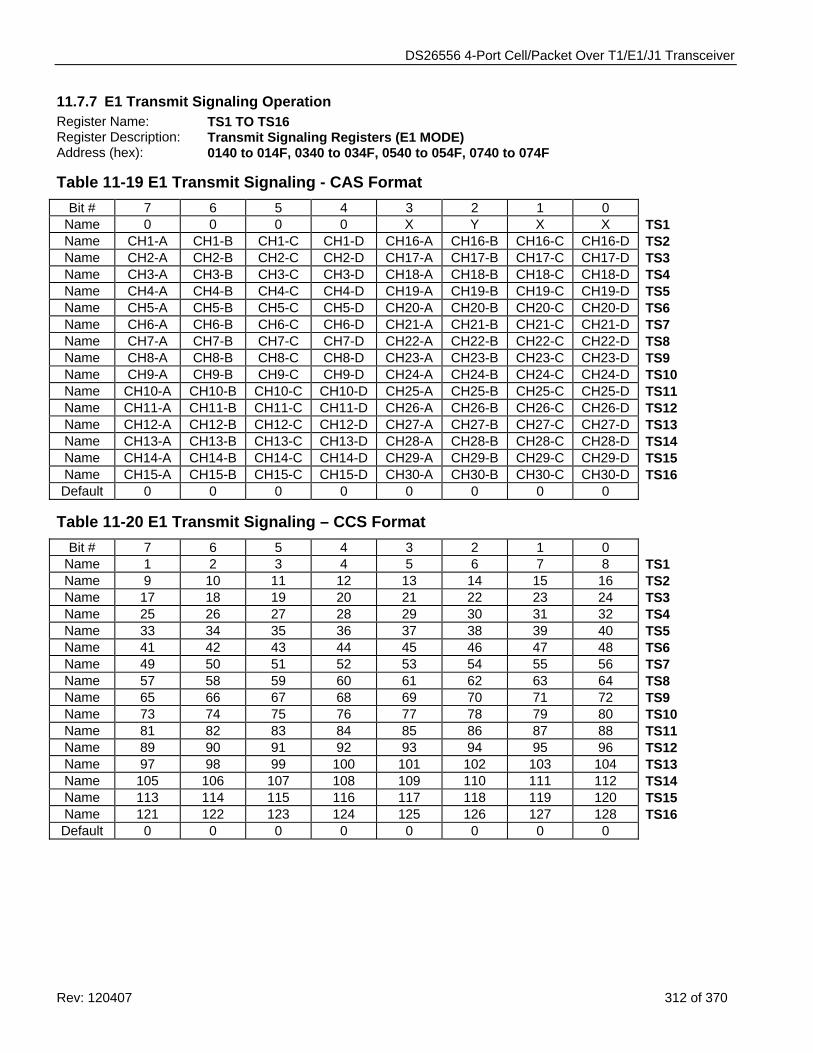
DS26556 4-Port Cell/Packet Over T1/E1/J1 Transceiver
Rev: 120407 312 of 370
11.7.7 E1 Transmit Signaling Operation Register Name: TS1 TO TS16 Register Description: Transmit Signaling Registers (E1 MODE) Address (hex): 0140 to 014F, 0340 to 034F, 0540 to 054F, 0740 to 074F
Table 11-19 E1 Transmit Signaling - CAS Format Bit # 7 6 5 4 3 2 1 0
Name 0 0 0 0 X Y X X TS1 Name CH1-A CH1-B CH1-C CH1-D CH16-A CH16-B CH16-C CH16-D TS2 Name CH2-A CH2-B CH2-C CH2-D CH17-A CH17-B CH17-C CH17-D TS3 Name CH3-A CH3-B CH3-C CH3-D CH18-A CH18-B CH18-C CH18-D TS4 Name CH4-A CH4-B CH4-C CH4-D CH19-A CH19-B CH19-C CH19-D TS5 Name CH5-A CH5-B CH5-C CH5-D CH20-A CH20-B CH20-C CH20-D TS6 Name CH6-A CH6-B CH6-C CH6-D CH21-A CH21-B CH21-C CH21-D TS7 Name CH7-A CH7-B CH7-C CH7-D CH22-A CH22-B CH22-C CH22-D TS8 Name CH8-A CH8-B CH8-C CH8-D CH23-A CH23-B CH23-C CH23-D TS9 Name CH9-A CH9-B CH9-C CH9-D CH24-A CH24-B CH24-C CH24-D TS10 Name CH10-A CH10-B CH10-C CH10-D CH25-A CH25-B CH25-C CH25-D TS11 Name CH11-A CH11-B CH11-C CH11-D CH26-A CH26-B CH26-C CH26-D TS12 Name CH12-A CH12-B CH12-C CH12-D CH27-A CH27-B CH27-C CH27-D TS13 Name CH13-A CH13-B CH13-C CH13-D CH28-A CH28-B CH28-C CH28-D TS14 Name CH14-A CH14-B CH14-C CH14-D CH29-A CH29-B CH29-C CH29-D TS15 Name CH15-A CH15-B CH15-C CH15-D CH30-A CH30-B CH30-C CH30-D TS16 Default 0 0 0 0 0 0 0 0
Table 11-20 E1 Transmit Signaling – CCS Format Bit # 7 6 5 4 3 2 1 0
Name 1 2 3 4 5 6 7 8 TS1 Name 9 10 11 12 13 14 15 16 TS2 Name 17 18 19 20 21 22 23 24 TS3 Name 25 26 27 28 29 30 31 32 TS4 Name 33 34 35 36 37 38 39 40 TS5 Name 41 42 43 44 45 46 47 48 TS6 Name 49 50 51 52 53 54 55 56 TS7 Name 57 58 59 60 61 62 63 64 TS8 Name 65 66 67 68 69 70 71 72 TS9 Name 73 74 75 76 77 78 79 80 TS10 Name 81 82 83 84 85 86 87 88 TS11 Name 89 90 91 92 93 94 95 96 TS12 Name 97 98 99 100 101 102 103 104 TS13 Name 105 106 107 108 109 110 111 112 TS14 Name 113 114 115 116 117 118 119 120 TS15 Name 121 122 123 124 125 126 127 128 TS16 Default 0 0 0 0 0 0 0 0
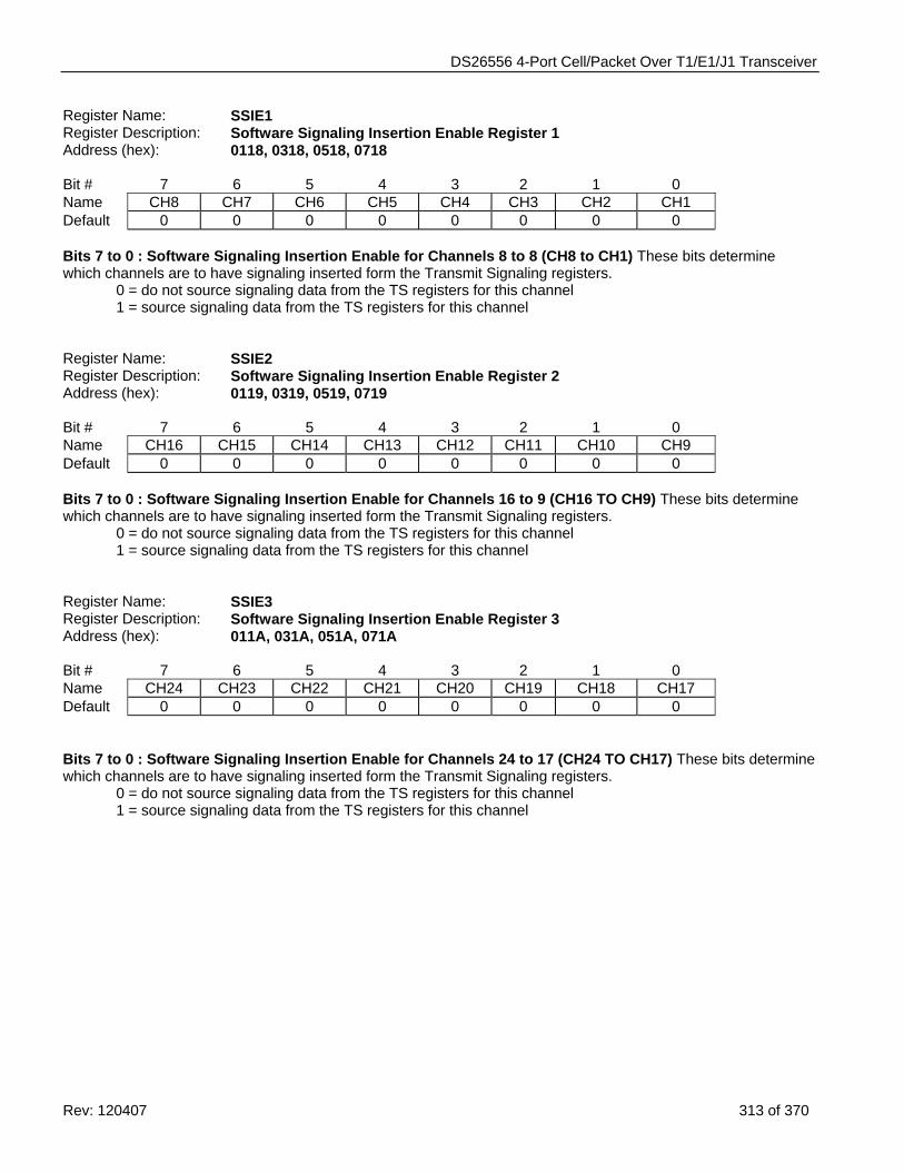
DS26556 4-Port Cell/Packet Over T1/E1/J1 Transceiver
Rev: 120407 313 of 370
Register Name: SSIE1 Register Description: Software Signaling Insertion Enable Register 1 Address (hex): 0118, 0318, 0518, 0718 Bit # 7 6 5 4 3 2 1 0 Name CH8 CH7 CH6 CH5 CH4 CH3 CH2 CH1 Default 0 0 0 0 0 0 0 0 Bits 7 to 0 : Software Signaling Insertion Enable for Channels 8 to 8 (CH8 to CH1) These bits determine which channels are to have signaling inserted form the Transmit Signaling registers.
0 = do not source signaling data from the TS registers for this channel 1 = source signaling data from the TS registers for this channel
Register Name: SSIE2 Register Description: Software Signaling Insertion Enable Register 2 Address (hex): 0119, 0319, 0519, 0719 Bit # 7 6 5 4 3 2 1 0 Name CH16 CH15 CH14 CH13 CH12 CH11 CH10 CH9 Default 0 0 0 0 0 0 0 0 Bits 7 to 0 : Software Signaling Insertion Enable for Channels 16 to 9 (CH16 TO CH9) These bits determine which channels are to have signaling inserted form the Transmit Signaling registers.
0 = do not source signaling data from the TS registers for this channel 1 = source signaling data from the TS registers for this channel
Register Name: SSIE3 Register Description: Software Signaling Insertion Enable Register 3 Address (hex): 011A, 031A, 051A, 071A Bit # 7 6 5 4 3 2 1 0 Name CH24 CH23 CH22 CH21 CH20 CH19 CH18 CH17 Default 0 0 0 0 0 0 0 0 Bits 7 to 0 : Software Signaling Insertion Enable for Channels 24 to 17 (CH24 TO CH17) These bits determine which channels are to have signaling inserted form the Transmit Signaling registers.
0 = do not source signaling data from the TS registers for this channel 1 = source signaling data from the TS registers for this channel
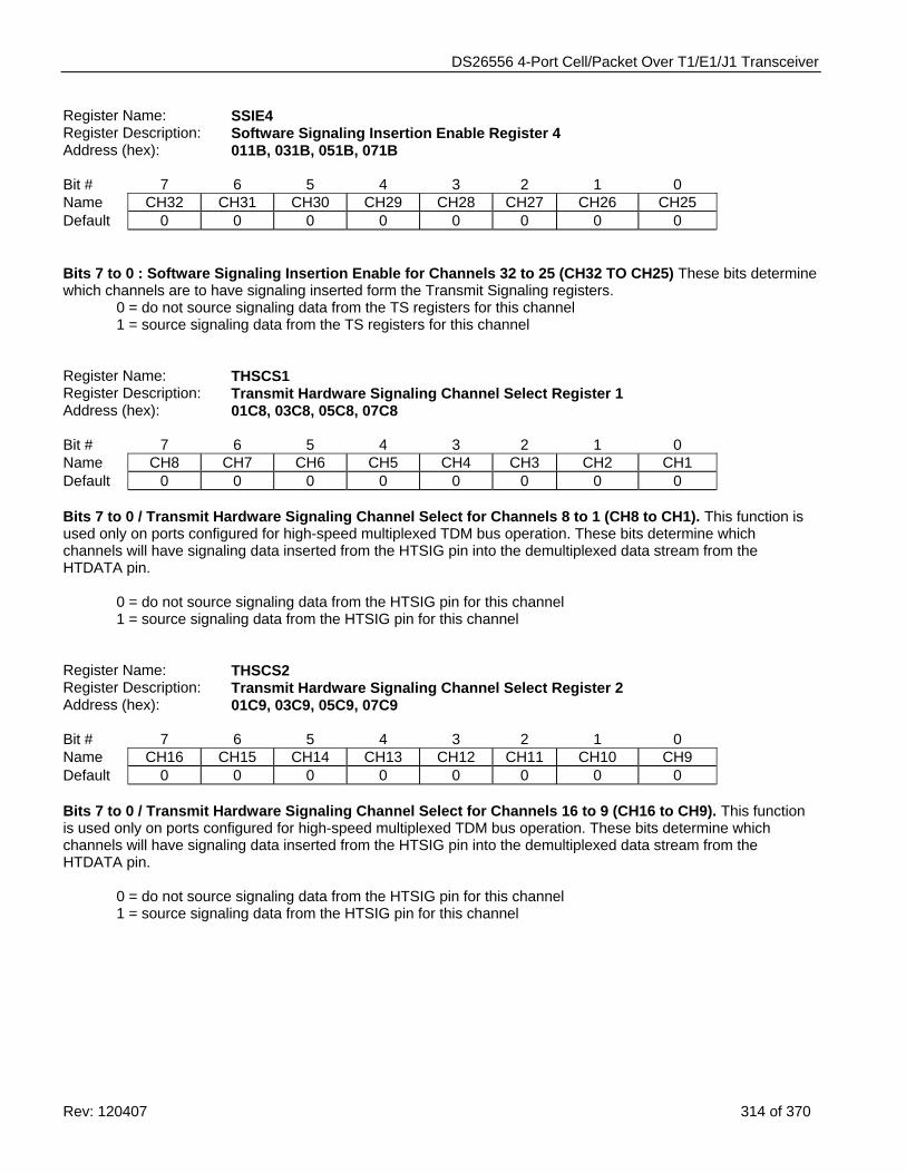
DS26556 4-Port Cell/Packet Over T1/E1/J1 Transceiver
Rev: 120407 314 of 370
Register Name: SSIE4 Register Description: Software Signaling Insertion Enable Register 4 Address (hex): 011B, 031B, 051B, 071B Bit # 7 6 5 4 3 2 1 0 Name CH32 CH31 CH30 CH29 CH28 CH27 CH26 CH25 Default 0 0 0 0 0 0 0 0 Bits 7 to 0 : Software Signaling Insertion Enable for Channels 32 to 25 (CH32 TO CH25) These bits determine which channels are to have signaling inserted form the Transmit Signaling registers.
0 = do not source signaling data from the TS registers for this channel 1 = source signaling data from the TS registers for this channel
Register Name: THSCS1 Register Description: Transmit Hardware Signaling Channel Select Register 1 Address (hex): 01C8, 03C8, 05C8, 07C8 Bit # 7 6 5 4 3 2 1 0 Name CH8 CH7 CH6 CH5 CH4 CH3 CH2 CH1 Default 0 0 0 0 0 0 0 0 Bits 7 to 0 / Transmit Hardware Signaling Channel Select for Channels 8 to 1 (CH8 to CH1). This function is used only on ports configured for high-speed multiplexed TDM bus operation. These bits determine which channels will have signaling data inserted from the HTSIG pin into the demultiplexed data stream from the HTDATA pin.
0 = do not source signaling data from the HTSIG pin for this channel 1 = source signaling data from the HTSIG pin for this channel
Register Name: THSCS2 Register Description: Transmit Hardware Signaling Channel Select Register 2 Address (hex): 01C9, 03C9, 05C9, 07C9 Bit # 7 6 5 4 3 2 1 0 Name CH16 CH15 CH14 CH13 CH12 CH11 CH10 CH9 Default 0 0 0 0 0 0 0 0 Bits 7 to 0 / Transmit Hardware Signaling Channel Select for Channels 16 to 9 (CH16 to CH9). This function is used only on ports configured for high-speed multiplexed TDM bus operation. These bits determine which channels will have signaling data inserted from the HTSIG pin into the demultiplexed data stream from the HTDATA pin.
0 = do not source signaling data from the HTSIG pin for this channel 1 = source signaling data from the HTSIG pin for this channel
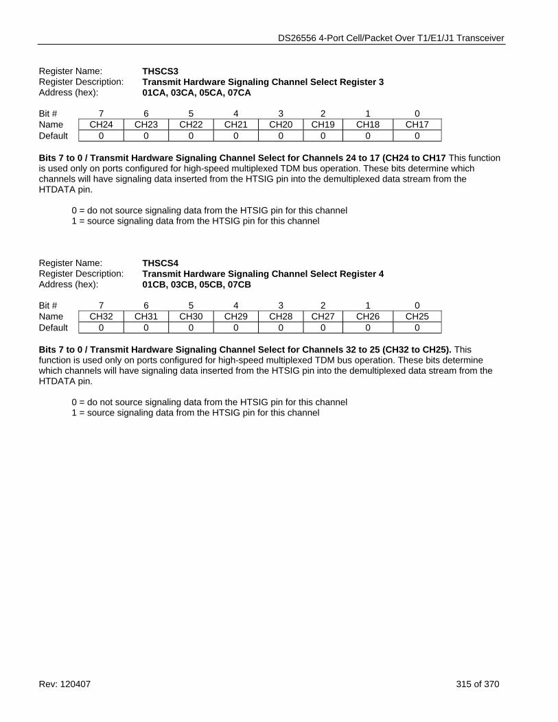
DS26556 4-Port Cell/Packet Over T1/E1/J1 Transceiver
Rev: 120407 315 of 370
Register Name: THSCS3 Register Description: Transmit Hardware Signaling Channel Select Register 3 Address (hex): 01CA, 03CA, 05CA, 07CA Bit # 7 6 5 4 3 2 1 0 Name CH24 CH23 CH22 CH21 CH20 CH19 CH18 CH17 Default 0 0 0 0 0 0 0 0 Bits 7 to 0 / Transmit Hardware Signaling Channel Select for Channels 24 to 17 (CH24 to CH17 This function is used only on ports configured for high-speed multiplexed TDM bus operation. These bits determine which channels will have signaling data inserted from the HTSIG pin into the demultiplexed data stream from the HTDATA pin.
0 = do not source signaling data from the HTSIG pin for this channel 1 = source signaling data from the HTSIG pin for this channel
Register Name: THSCS4 Register Description: Transmit Hardware Signaling Channel Select Register 4 Address (hex): 01CB, 03CB, 05CB, 07CB Bit # 7 6 5 4 3 2 1 0 Name CH32 CH31 CH30 CH29 CH28 CH27 CH26 CH25 Default 0 0 0 0 0 0 0 0 Bits 7 to 0 / Transmit Hardware Signaling Channel Select for Channels 32 to 25 (CH32 to CH25). This function is used only on ports configured for high-speed multiplexed TDM bus operation. These bits determine which channels will have signaling data inserted from the HTSIG pin into the demultiplexed data stream from the HTDATA pin.
0 = do not source signaling data from the HTSIG pin for this channel 1 = source signaling data from the HTSIG pin for this channel
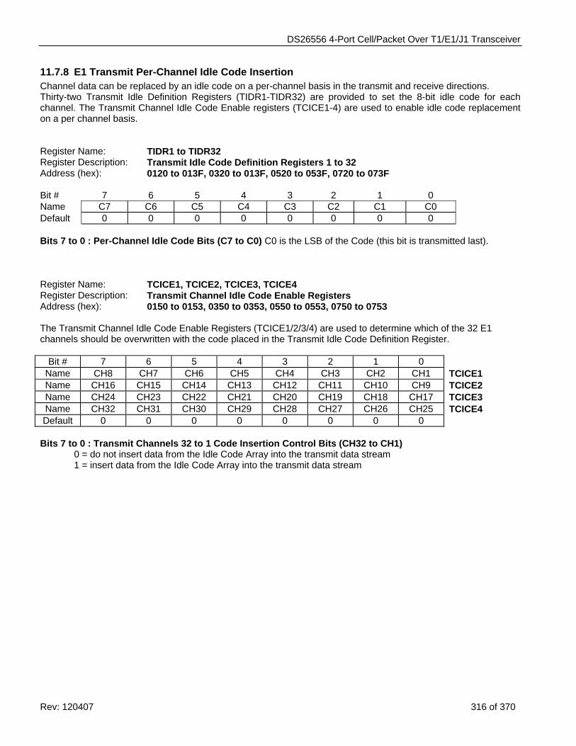
DS26556 4-Port Cell/Packet Over T1/E1/J1 Transceiver
Rev: 120407 316 of 370
11.7.8 E1 Transmit Per-Channel Idle Code Insertion Channel data can be replaced by an idle code on a per-channel basis in the transmit and receive directions. Thirty-two Transmit Idle Definition Registers (TIDR1-TIDR32) are provided to set the 8-bit idle code for each channel. The Transmit Channel Idle Code Enable registers (TCICE1-4) are used to enable idle code replacement on a per channel basis. Register Name: TIDR1 to TIDR32 Register Description: Transmit Idle Code Definition Registers 1 to 32 Address (hex): 0120 to 013F, 0320 to 013F, 0520 to 053F, 0720 to 073F Bit # 7 6 5 4 3 2 1 0 Name C7 C6 C5 C4 C3 C2 C1 C0 Default 0 0 0 0 0 0 0 0 Bits 7 to 0 : Per-Channel Idle Code Bits (C7 to C0) C0 is the LSB of the Code (this bit is transmitted last). Register Name: TCICE1, TCICE2, TCICE3, TCICE4 Register Description: Transmit Channel Idle Code Enable Registers Address (hex): 0150 to 0153, 0350 to 0353, 0550 to 0553, 0750 to 0753 The Transmit Channel Idle Code Enable Registers (TCICE1/2/3/4) are used to determine which of the 32 E1 channels should be overwritten with the code placed in the Transmit Idle Code Definition Register.
Bit # 7 6 5 4 3 2 1 0 Name CH8 CH7 CH6 CH5 CH4 CH3 CH2 CH1 TCICE1 Name CH16 CH15 CH14 CH13 CH12 CH11 CH10 CH9 TCICE2 Name CH24 CH23 CH22 CH21 CH20 CH19 CH18 CH17 TCICE3 Name CH32 CH31 CH30 CH29 CH28 CH27 CH26 CH25 TCICE4 Default 0 0 0 0 0 0 0 0
Bits 7 to 0 : Transmit Channels 32 to 1 Code Insertion Control Bits (CH32 to CH1)
0 = do not insert data from the Idle Code Array into the transmit data stream 1 = insert data from the Idle Code Array into the transmit data stream
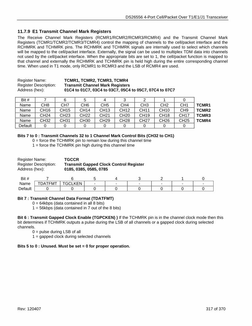
DS26556 4-Port Cell/Packet Over T1/E1/J1 Transceiver
Rev: 120407 317 of 370
11.7.9 E1 Transmit Channel Mark Registers The Receive Channel Mark Registers (RCMR1/RCMR2/RCMR3/RCMR4) and the Transmit Channel Mark Registers (TCMR1/TCMR2/TCMR3/TCMR4) control the mapping of channels to the cell/packet interface and the RCHMRK and TCHMRK pins. The RCHMRK and TCHMRK signals are internally used to select which channels will be mapped to the cell/packet interface. Externally, the signal can be used to multiplex TDM data into channels not used by the cell/packet interface. When the appropriate bits are set to 1, the cell/packet function is mapped to that channel and externally the RCHMRK and TCHMRK pin is held high during the entire corresponding channel time. When used in T1 mode, only RCMR1 to RCMR3 and the LSB of RCMR4 are used. Register Name: TCMR1, TCMR2, TCMR3, TCMR4 Register Description: Transmit Channel Mark Registers Address (hex): 01C4 to 01C7, 03C4 to 03C7, 05C4 to 05C7, 07C4 to 07C7
Bit # 7 6 5 4 3 2 1 0 Name CH8 CH7 CH6 CH5 CH4 CH3 CH2 CH1 TCMR1 Name CH16 CH15 CH14 CH13 CH12 CH11 CH10 CH9 TCMR2 Name CH24 CH23 CH22 CH21 CH20 CH19 CH18 CH17 TCMR3 Name CH32 CH31 CH30 CH29 CH28 CH27 CH26 CH25 TCMR4 Default 0 0 0 0 0 0 0 0
Bits 7 to 0 : Transmit Channels 32 to 1 Channel Mark Control Bits (CH32 to CH1)
0 = force the TCHMRK pin to remain low during this channel time 1 = force the TCHMRK pin high during this channel time
Register Name: TGCCR Register Description: Transmit Gapped Clock Control Register Address (hex): 0185, 0385, 0585, 0785
Bit # 7 6 5 4 3 2 1 0 Name TDATFMT TGCLKEN - - - - - - Default 0 0 0 0 0 0 0 0 Bit 7 : Transmit Channel Data Format (TDATFMT)
0 = 64kbps (data contained in all 8 bits) 1 = 56kbps (data contained in 7 out of the 8 bits)
Bit 6 : Transmit Gapped Clock Enable (TGPCKEN) ) If the TCHMRK pin is in the channel clock mode then this bit determines if TCHMRK outputs a pulse during the LSB of all channels or a gapped clock during selected channels.
0 = pulse during LSB of all 1 = gapped clock during selected channels
Bits 5 to 0 : Unused. Must be set = 0 for proper operation.
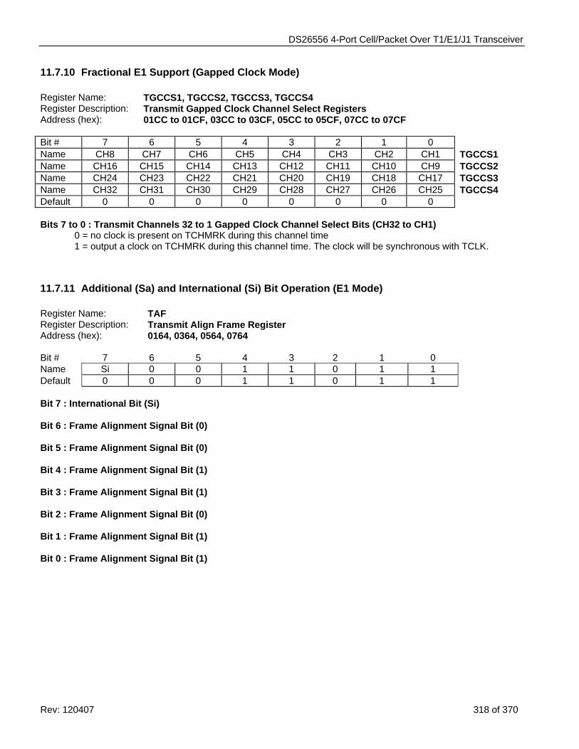
DS26556 4-Port Cell/Packet Over T1/E1/J1 Transceiver
Rev: 120407 318 of 370
11.7.10 Fractional E1 Support (Gapped Clock Mode) Register Name: TGCCS1, TGCCS2, TGCCS3, TGCCS4 Register Description: Transmit Gapped Clock Channel Select Registers Address (hex): 01CC to 01CF, 03CC to 03CF, 05CC to 05CF, 07CC to 07CF Bit # 7 6 5 4 3 2 1 0 Name CH8 CH7 CH6 CH5 CH4 CH3 CH2 CH1 TGCCS1 Name CH16 CH15 CH14 CH13 CH12 CH11 CH10 CH9 TGCCS2 Name CH24 CH23 CH22 CH21 CH20 CH19 CH18 CH17 TGCCS3 Name CH32 CH31 CH30 CH29 CH28 CH27 CH26 CH25 TGCCS4 Default 0 0 0 0 0 0 0 0 Bits 7 to 0 : Transmit Channels 32 to 1 Gapped Clock Channel Select Bits (CH32 to CH1)
0 = no clock is present on TCHMRK during this channel time 1 = output a clock on TCHMRK during this channel time. The clock will be synchronous with TCLK.
11.7.11 Additional (Sa) and International (Si) Bit Operation (E1 Mode) Register Name: TAF Register Description: Transmit Align Frame Register Address (hex): 0164, 0364, 0564, 0764 Bit # 7 6 5 4 3 2 1 0 Name Si 0 0 1 1 0 1 1 Default 0 0 0 1 1 0 1 1 Bit 7 : International Bit (Si) Bit 6 : Frame Alignment Signal Bit (0) Bit 5 : Frame Alignment Signal Bit (0) Bit 4 : Frame Alignment Signal Bit (1) Bit 3 : Frame Alignment Signal Bit (1) Bit 2 : Frame Alignment Signal Bit (0) Bit 1 : Frame Alignment Signal Bit (1) Bit 0 : Frame Alignment Signal Bit (1)
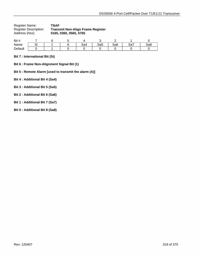
DS26556 4-Port Cell/Packet Over T1/E1/J1 Transceiver
Rev: 120407 319 of 370
Register Name: TNAF Register Description: Transmit Non-Align Frame Register Address (hex): 0165, 0365, 0565, 0765 Bit # 7 6 5 4 3 2 1 0 Name Si 1 A Sa4 Sa5 Sa6 Sa7 Sa8 Default 0 1 0 0 0 0 0 0 Bit 7 : International Bit (Si) Bit 6 : Frame Non-Alignment Signal Bit (1) Bit 5 : Remote Alarm [used to transmit the alarm (A)] Bit 4 : Additional Bit 4 (Sa4) Bit 3 : Additional Bit 5 (Sa5) Bit 2 : Additional Bit 6 (Sa6) Bit 1 : Additional Bit 7 (Sa7) Bit 0 : Additional Bit 8 (Sa8)
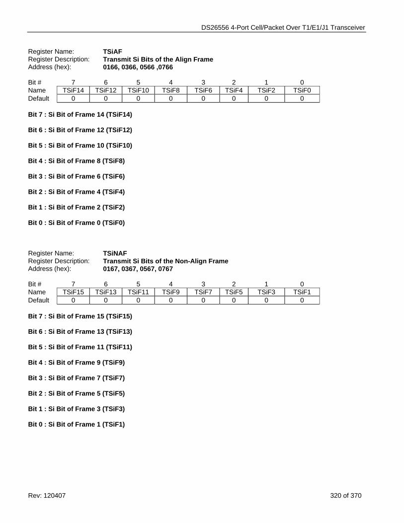
DS26556 4-Port Cell/Packet Over T1/E1/J1 Transceiver
Rev: 120407 320 of 370
Register Name: TSiAF Register Description: Transmit Si Bits of the Align Frame Address (hex): 0166, 0366, 0566 ,0766 Bit # 7 6 5 4 3 2 1 0 Name TSiF14 TSiF12 TSiF10 TSiF8 TSiF6 TSiF4 TSiF2 TSiF0 Default 0 0 0 0 0 0 0 0 Bit 7 : Si Bit of Frame 14 (TSiF14) Bit 6 : Si Bit of Frame 12 (TSiF12) Bit 5 : Si Bit of Frame 10 (TSiF10) Bit 4 : Si Bit of Frame 8 (TSiF8) Bit 3 : Si Bit of Frame 6 (TSiF6) Bit 2 : Si Bit of Frame 4 (TSiF4) Bit 1 : Si Bit of Frame 2 (TSiF2) Bit 0 : Si Bit of Frame 0 (TSiF0) Register Name: TSiNAF Register Description: Transmit Si Bits of the Non-Align Frame Address (hex): 0167, 0367, 0567, 0767 Bit # 7 6 5 4 3 2 1 0 Name TSiF15 TSiF13 TSiF11 TSiF9 TSiF7 TSiF5 TSiF3 TSiF1 Default 0 0 0 0 0 0 0 0 Bit 7 : Si Bit of Frame 15 (TSiF15) Bit 6 : Si Bit of Frame 13 (TSiF13) Bit 5 : Si Bit of Frame 11 (TSiF11) Bit 4 : Si Bit of Frame 9 (TSiF9) Bit 3 : Si Bit of Frame 7 (TSiF7) Bit 2 : Si Bit of Frame 5 (TSiF5) Bit 1 : Si Bit of Frame 3 (TSiF3) Bit 0 : Si Bit of Frame 1 (TSiF1)
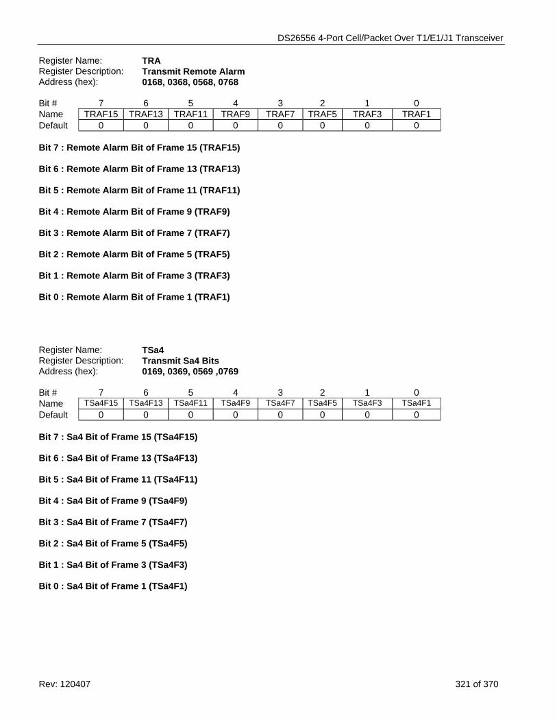
DS26556 4-Port Cell/Packet Over T1/E1/J1 Transceiver
Rev: 120407 321 of 370
Register Name: TRA Register Description: Transmit Remote Alarm Address (hex): 0168, 0368, 0568, 0768 Bit # 7 6 5 4 3 2 1 0 Name TRAF15 TRAF13 TRAF11 TRAF9 TRAF7 TRAF5 TRAF3 TRAF1 Default 0 0 0 0 0 0 0 0 Bit 7 : Remote Alarm Bit of Frame 15 (TRAF15) Bit 6 : Remote Alarm Bit of Frame 13 (TRAF13) Bit 5 : Remote Alarm Bit of Frame 11 (TRAF11) Bit 4 : Remote Alarm Bit of Frame 9 (TRAF9) Bit 3 : Remote Alarm Bit of Frame 7 (TRAF7) Bit 2 : Remote Alarm Bit of Frame 5 (TRAF5) Bit 1 : Remote Alarm Bit of Frame 3 (TRAF3) Bit 0 : Remote Alarm Bit of Frame 1 (TRAF1) Register Name: TSa4 Register Description: Transmit Sa4 Bits Address (hex): 0169, 0369, 0569 ,0769 Bit # 7 6 5 4 3 2 1 0 Name TSa4F15 TSa4F13 TSa4F11 TSa4F9 TSa4F7 TSa4F5 TSa4F3 TSa4F1 Default 0 0 0 0 0 0 0 0 Bit 7 : Sa4 Bit of Frame 15 (TSa4F15) Bit 6 : Sa4 Bit of Frame 13 (TSa4F13) Bit 5 : Sa4 Bit of Frame 11 (TSa4F11) Bit 4 : Sa4 Bit of Frame 9 (TSa4F9) Bit 3 : Sa4 Bit of Frame 7 (TSa4F7) Bit 2 : Sa4 Bit of Frame 5 (TSa4F5) Bit 1 : Sa4 Bit of Frame 3 (TSa4F3) Bit 0 : Sa4 Bit of Frame 1 (TSa4F1)
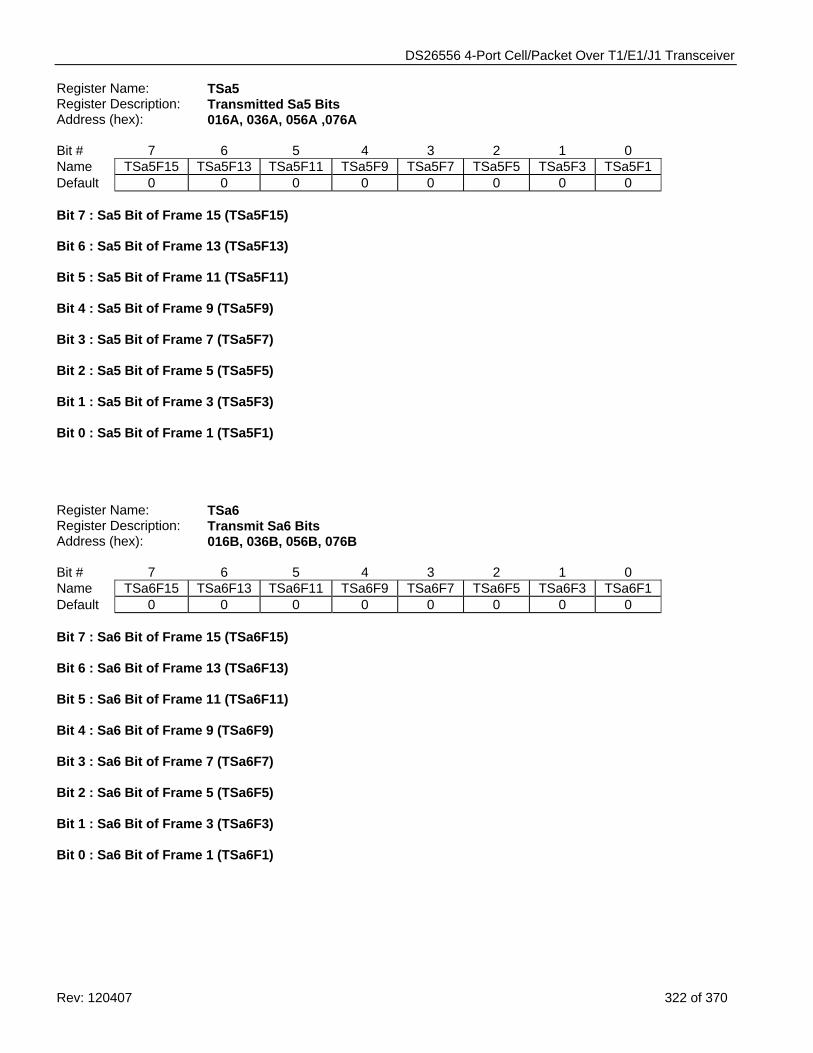
DS26556 4-Port Cell/Packet Over T1/E1/J1 Transceiver
Rev: 120407 322 of 370
Register Name: TSa5 Register Description: Transmitted Sa5 Bits Address (hex): 016A, 036A, 056A ,076A Bit # 7 6 5 4 3 2 1 0 Name TSa5F15 TSa5F13 TSa5F11 TSa5F9 TSa5F7 TSa5F5 TSa5F3 TSa5F1 Default 0 0 0 0 0 0 0 0 Bit 7 : Sa5 Bit of Frame 15 (TSa5F15) Bit 6 : Sa5 Bit of Frame 13 (TSa5F13) Bit 5 : Sa5 Bit of Frame 11 (TSa5F11) Bit 4 : Sa5 Bit of Frame 9 (TSa5F9) Bit 3 : Sa5 Bit of Frame 7 (TSa5F7) Bit 2 : Sa5 Bit of Frame 5 (TSa5F5) Bit 1 : Sa5 Bit of Frame 3 (TSa5F3) Bit 0 : Sa5 Bit of Frame 1 (TSa5F1) Register Name: TSa6 Register Description: Transmit Sa6 Bits Address (hex): 016B, 036B, 056B, 076B Bit # 7 6 5 4 3 2 1 0 Name TSa6F15 TSa6F13 TSa6F11 TSa6F9 TSa6F7 TSa6F5 TSa6F3 TSa6F1 Default 0 0 0 0 0 0 0 0 Bit 7 : Sa6 Bit of Frame 15 (TSa6F15) Bit 6 : Sa6 Bit of Frame 13 (TSa6F13) Bit 5 : Sa6 Bit of Frame 11 (TSa6F11) Bit 4 : Sa6 Bit of Frame 9 (TSa6F9) Bit 3 : Sa6 Bit of Frame 7 (TSa6F7) Bit 2 : Sa6 Bit of Frame 5 (TSa6F5) Bit 1 : Sa6 Bit of Frame 3 (TSa6F3) Bit 0 : Sa6 Bit of Frame 1 (TSa6F1)
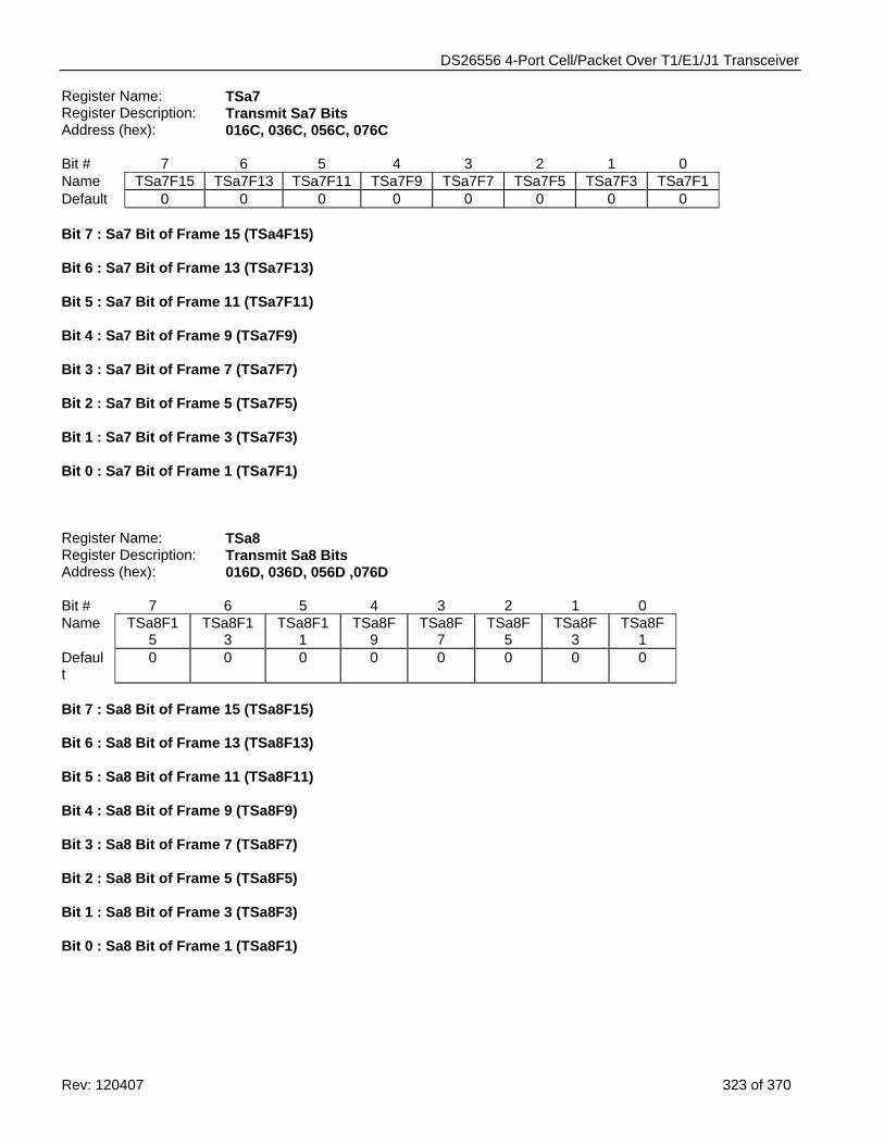
DS26556 4-Port Cell/Packet Over T1/E1/J1 Transceiver
Rev: 120407 323 of 370
Register Name: TSa7 Register Description: Transmit Sa7 Bits Address (hex): 016C, 036C, 056C, 076C Bit # 7 6 5 4 3 2 1 0 Name TSa7F15 TSa7F13 TSa7F11 TSa7F9 TSa7F7 TSa7F5 TSa7F3 TSa7F1 Default 0 0 0 0 0 0 0 0 Bit 7 : Sa7 Bit of Frame 15 (TSa4F15) Bit 6 : Sa7 Bit of Frame 13 (TSa7F13) Bit 5 : Sa7 Bit of Frame 11 (TSa7F11) Bit 4 : Sa7 Bit of Frame 9 (TSa7F9) Bit 3 : Sa7 Bit of Frame 7 (TSa7F7) Bit 2 : Sa7 Bit of Frame 5 (TSa7F5) Bit 1 : Sa7 Bit of Frame 3 (TSa7F3) Bit 0 : Sa7 Bit of Frame 1 (TSa7F1) Register Name: TSa8 Register Description: Transmit Sa8 Bits Address (hex): 016D, 036D, 056D ,076D Bit # 7 6 5 4 3 2 1 0 Name TSa8F1
5 TSa8F1
3 TSa8F1
1 TSa8F
9 TSa8F
7 TSa8F
5 TSa8F
3 TSa8F
1 Default
0 0 0 0 0 0 0 0
Bit 7 : Sa8 Bit of Frame 15 (TSa8F15) Bit 6 : Sa8 Bit of Frame 13 (TSa8F13) Bit 5 : Sa8 Bit of Frame 11 (TSa8F11) Bit 4 : Sa8 Bit of Frame 9 (TSa8F9) Bit 3 : Sa8 Bit of Frame 7 (TSa8F7) Bit 2 : Sa8 Bit of Frame 5 (TSa8F5) Bit 1 : Sa8 Bit of Frame 3 (TSa8F3) Bit 0 : Sa8 Bit of Frame 1 (TSa8F1)
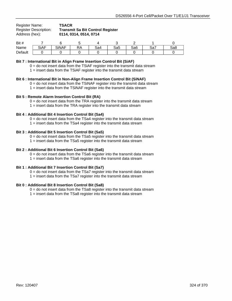
DS26556 4-Port Cell/Packet Over T1/E1/J1 Transceiver
Rev: 120407 324 of 370
Register Name: TSACR Register Description: Transmit Sa Bit Control Register Address (hex): 0114, 0314, 0514, 0714 Bit # 7 6 5 4 3 2 1 0 Name SiAF SiNAF RA Sa4 Sa5 Sa6 Sa7 Sa8 Default 0 0 0 0 0 0 0 0 Bit 7 : International Bit in Align Frame Insertion Control Bit (SiAF)
0 = do not insert data from the TSiAF register into the transmit data stream 1 = insert data from the TSiAF register into the transmit data stream
Bit 6 : International Bit in Non-Align Frame Insertion Control Bit (SiNAF)
0 = do not insert data from the TSiNAF register into the transmit data stream 1 = insert data from the TSiNAF register into the transmit data stream
Bit 5 : Remote Alarm Insertion Control Bit (RA)
0 = do not insert data from the TRA register into the transmit data stream 1 = insert data from the TRA register into the transmit data stream
Bit 4 : Additional Bit 4 Insertion Control Bit (Sa4)
0 = do not insert data from the TSa4 register into the transmit data stream 1 = insert data from the TSa4 register into the transmit data stream
Bit 3 : Additional Bit 5 Insertion Control Bit (Sa5)
0 = do not insert data from the TSa5 register into the transmit data stream 1 = insert data from the TSa5 register into the transmit data stream
Bit 2 : Additional Bit 6 Insertion Control Bit (Sa6)
0 = do not insert data from the TSa6 register into the transmit data stream 1 = insert data from the TSa6 register into the transmit data stream
Bit 1 : Additional Bit 7 Insertion Control Bit (Sa7)
0 = do not insert data from the TSa7 register into the transmit data stream 1 = insert data from the TSa7 register into the transmit data stream
Bit 0 : Additional Bit 8 Insertion Control Bit (Sa8)
0 = do not insert data from the TSa8 register into the transmit data stream 1 = insert data from the TSa8 register into the transmit data stream
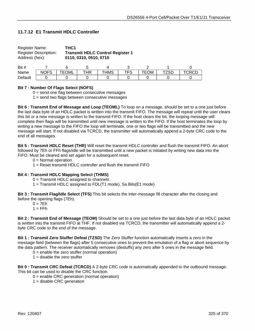
DS26556 4-Port Cell/Packet Over T1/E1/J1 Transceiver
Rev: 120407 325 of 370
11.7.12 E1 Transmit HDLC Controller Register Name: THC1 Register Description: Transmit HDLC Control Register 1 Address (hex): 0110, 0310, 0510, 0710 Bit # 7 6 5 4 3 2 1 0 Name NOFS TEOML THR THMS TFS TEOM TZSD TCRCD Default 0 0 0 0 0 0 0 0 Bit 7 : Number Of Flags Select (NOFS) 0 = send one flag between consecutive messages 1 = send two flags between consecutive messages Bit 6 : Transmit End of Message and Loop (TEOML) To loop on a message, should be set to a one just before the last data byte of an HDLC packet is written into the transmit FIFO. The message will repeat until the user clears this bit or a new message is written to the transmit FIFO. If the host clears the bit, the looping message will complete then flags will be transmitted until new message is written to the FIFO. If the host terminates the loop by writing a new message to the FIFO the loop will terminate, one or two flags will be transmitted and the new message will start. If not disabled via TCRCD, the transmitter will automatically append a 2-byte CRC code to the end of all messages. Bit 5 : Transmit HDLC Reset (THR) Will reset the transmit HDLC controller and flush the transmit FIFO. An abort followed by 7Eh or FFh flags/idle will be transmitted until a new packet is initiated by writing new data into the FIFO. Must be cleared and set again for a subsequent reset. 0 = Normal operation 1 = Reset transmit HDLC controller and flush the transmit FIFO Bit 4 : Transmit HDLC Mapping Select (THMS)
0 = Transmit HDLC assigned to channels 1 = Transmit HDLC assigned to FDL(T1 mode), Sa Bits(E1 mode)
Bit 3 : Transmit Flag/Idle Select (TFS) This bit selects the inter-message fill character after the closing and before the opening flags (7Eh).
0 = 7Eh 1 = FFh
Bit 2 : Transmit End of Message (TEOM) Should be set to a one just before the last data byte of an HDLC packet is written into the transmit FIFO at THF. If not disabled via TCRCD, the transmitter will automatically append a 2-byte CRC code to the end of the message. Bit 1 : Transmit Zero Stuffer Defeat (TZSD) The Zero Stuffer function automatically inserts a zero in the message field (between the flags) after 5 consecutive ones to prevent the emulation of a flag or abort sequence by the data pattern. The receiver automatically removes (destuffs) any zero after 5 ones in the message field.
0 = enable the zero stuffer (normal operation) 1 = disable the zero stuffer
Bit 0 : Transmit CRC Defeat (TCRCD) A 2-byte CRC code is automatically appended to the outbound message. This bit can be used to disable the CRC function.
0 = enable CRC generation (normal operation) 1 = disable CRC generation
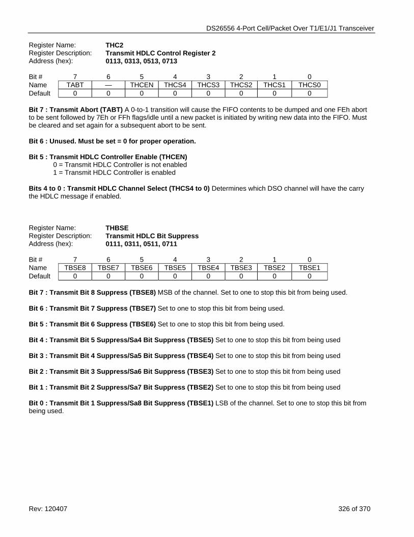
DS26556 4-Port Cell/Packet Over T1/E1/J1 Transceiver
Rev: 120407 326 of 370
Register Name: THC2 Register Description: Transmit HDLC Control Register 2 Address (hex): 0113, 0313, 0513, 0713 Bit # 7 6 5 4 3 2 1 0 Name TABT — THCEN THCS4 THCS3 THCS2 THCS1 THCS0 Default 0 0 0 0 0 0 0 0 Bit 7 : Transmit Abort (TABT) A 0-to-1 transition will cause the FIFO contents to be dumped and one FEh abort to be sent followed by 7Eh or FFh flags/idle until a new packet is initiated by writing new data into the FIFO. Must be cleared and set again for a subsequent abort to be sent. Bit 6 : Unused. Must be set = 0 for proper operation. Bit 5 : Transmit HDLC Controller Enable (THCEN) 0 = Transmit HDLC Controller is not enabled 1 = Transmit HDLC Controller is enabled Bits 4 to 0 : Transmit HDLC Channel Select (THCS4 to 0) Determines which DSO channel will have the carry the HDLC message if enabled. Register Name: THBSE Register Description: Transmit HDLC Bit Suppress Address (hex): 0111, 0311, 0511, 0711 Bit # 7 6 5 4 3 2 1 0 Name TBSE8 TBSE7 TBSE6 TBSE5 TBSE4 TBSE3 TBSE2 TBSE1 Default 0 0 0 0 0 0 0 0 Bit 7 : Transmit Bit 8 Suppress (TBSE8) MSB of the channel. Set to one to stop this bit from being used. Bit 6 : Transmit Bit 7 Suppress (TBSE7) Set to one to stop this bit from being used. Bit 5 : Transmit Bit 6 Suppress (TBSE6) Set to one to stop this bit from being used. Bit 4 : Transmit Bit 5 Suppress/Sa4 Bit Suppress (TBSE5) Set to one to stop this bit from being used Bit 3 : Transmit Bit 4 Suppress/Sa5 Bit Suppress (TBSE4) Set to one to stop this bit from being used Bit 2 : Transmit Bit 3 Suppress/Sa6 Bit Suppress (TBSE3) Set to one to stop this bit from being used Bit 1 : Transmit Bit 2 Suppress/Sa7 Bit Suppress (TBSE2) Set to one to stop this bit from being used Bit 0 : Transmit Bit 1 Suppress/Sa8 Bit Suppress (TBSE1) LSB of the channel. Set to one to stop this bit from being used.
DS26556 4-Port Cell/Packet Over T1/E1/J1 Transceiver
Rev: 120407 327 of 370
11.7.12.1 Transmit HDLC FIFO Control Control of the transmit FIFO is accomplished via the Transmit HDLC FIFO Control (THFC). The FIFO Control register sets the watermarks for the receive FIFO.
When the transmit FIFO empties below the low watermark, the TLWM bit in the appropriate HDLC status register will be set. TLWM is a real-time bit and will remain set as long as the transmit FIFO’s write pointer is below the watermark. If enabled, this condition can also cause an interrupt via the INT pin. Register Name: THFC Register Description: Transmit HDLC FIFO Control Register Address (hex): 0187, 0387, 0587, 0787 Bit # 7 6 5 4 3 2 1 0 Name — — — — — — TFLWM1 TFLWM0 Default 0 0 0 0 0 0 0 0 Bits 7 to 2 : Unused. Must be set = 0 for proper operation. Bits 1 & 0 : Transmit HDLC FIFO Low-Watermark Select (TFLWM1 to TFLWM0)
TFLWM1 TFLWM0 Transmit FIFO Watermark 0 0 4 bytes 0 1 16 bytes 1 0 32 bytes 1 1 48 bytes
11.7.12.2 HDLC Status and Information TLS2 provides status information for the transmit HDLC controller. When a particular event has occurred (or is occurring), the appropriate bit in one of these registers will be set to a one. Some of the bits in these registers are latched and some are real-time bits that are not latched. This section contains register descriptions that list which bits are latched and which are real time. With the latched bits, when an event occurs and a bit is set to a one, it will remain set until the user reads that bit. The bit will be cleared when it is read and it will not be set again until the event has occurred again. The real-time bits report the current instantaneous conditions that are occurring and the history of these bits is not latched.
Like the other latched status registers, the user will follow a read of the status bit with a write. The byte written to the register will inform the device which of the latched bits the user wishes to clear (the real time bits are not affected by writing to the status register). The user will write a byte to one of these registers, with a one in the bit positions he or she wishes to clear and a zero in the bit positions he or she does not wish to clear.
The HDLC status register, TLS2 has the ability to initiate a hardware interrupt via the INT output signal. Each of the events in this register can be either masked or unmasked from the interrupt pin via the receive HDLC Interrupt Mask Register (TIM2). Interrupts will force the INT signal low when the event occurs. The INT pin will be allowed to return high (if no other interrupts are present) when the user reads the event bit that caused the interrupt to occur.
DS26556 4-Port Cell/Packet Over T1/E1/J1 Transceiver
Rev: 120407 328 of 370
Register Name: TRTS2 Register Description: Transmit Real-Time Status Register 2 (HDLC) Address (hex): 01B1, 03B1, 05B1, 07B1 Bit # 7 6 5 4 3 2 1 0 Name — — — — TEMPTY TFULL TLWM TNF Default 0 0 0 0 0 0 0 0
All bits in this register are real time. Bits 7 to 4 : Unused. Bit 3 : Transmit FIFO Empty (TEMPTY) A real-time bit that is set high when the FIFO is empty. Bit 2 : Transmit FIFO Full (TFULL) A real-time bit that is set high when the FIFO is full. Bit 1 : Transmit FIFO Below Low-Watermark Condition (TLWM) Set when the transmit 64-byte FIFO empties below the low watermark as defined by the Transmit Low-Watermark bits (TLWM). Bit 0 : Transmit FIFO Not Full Condition (TNF) Set when the transmit 64-byte FIFO has at least one byte available.
DS26556 4-Port Cell/Packet Over T1/E1/J1 Transceiver
Rev: 120407 329 of 370
Register Name: TLS2 Register Description: Transmit Latched Status Register 2 (HDLC) Address (hex): 0191, 0391, 0591, 0791 Bit # 7 6 5 4 3 2 1 0 Name — — — — TUDR TMEND TLWMS TNFS Default 0 0 0 0 0 0 0 0
All bits in this register are latched and can create interrupts. Bits 7 to 4 : Unused. Bit 3 : Transmit FIFO Underrun Event (TUDR) Set when the transmit FIFO empties out without having seen the TMEND bit set. An abort is automatically sent. Bit 2 : Transmit Message End Event (TMEND) Set when the transmit HDLC controller has finished sending a message. Bit 1 : Transmit FIFO Below Low-Watermark Set Condition (TLWMS) Set when the transmit 64-byte FIFO empties beyond the low watermark as defined by the Transmit Low-Watermark bits (TLWM) (rising edge detect of TLWM). Bit 0 : Transmit FIFO Not Full Set Condition (TNFS) Set when the transmit 64-byte FIFO has at least one empty byte available for write. Rising edge detect of TNF. Indicates change of state from full to not full. Register Name: TIM2 Register Description: Transmit Interrupt Mask Register 2 Address (hex): 01A1, 03A1, 05A1, 07A1 Bit # 7 6 5 4 3 2 1 0 Name — — — — TUDR TMEND TLWMS TNFS Default 0 0 0 0 0 0 0 0 Bits 7 to 4 : Unused. Must be set = 0 for proper operation. Bit 3 : Transmit FIFO Underrun Event (TUDR)
0 = interrupt masked 1 = interrupt enabled
Bit 2 : Transmit Message End Event (TMEND)
0 = interrupt masked 1 = interrupt enabled
Bit 1 : Transmit FIFO Below Low Watermark Set Condition (TLWMS)
0 = interrupt masked 1 = interrupt enabled
Bit 0 : Transmit FIFO Not Full Set Condition (TNFS)
0 = interrupt masked 1 = interrupt enabled

DS26556 4-Port Cell/Packet Over T1/E1/J1 Transceiver
Rev: 120407 330 of 370
11.7.12.3 FIFO Information The Transmit FIFO Buffer Available register indicates the number of bytes that can be written into the transmit FIFO. The count form this register informs the host as to how many bytes can be written into the transmit FIFO without overflowing the buffer. This is a real-time register. The count shall remain valid and stable during the read cycle. Register Name: TFBA Register Description: Transmit HDLC FIFO Buffer Available Address (hex): 01B3, 03B3, 05B3, 07B3 Bit # 7 6 5 4 3 2 1 0 Name — TFBA6 TFBA5 TFBA4 TFBA3 TFBA2 TFBA1 TFBA0 Default 0 0 0 0 0 0 0 0 Bit 7 : Unused. Bits 6 to 0 : Transmit FIFO Bytes Available (TFBA6 to TFBA0) TFBA0 is the LSB. Register Name: THF Register Description: Transmit HDLC FIFO Address (hex): 01B4, 03B4, 05B4, 07B4 Bit # 7 6 5 4 3 2 1 0 Name THD7 THD6 THD5 THD4 THD3 THD2 THD1 THD0 Default 0 0 0 0 0 0 0 0 Bit 7 : Transmit HDLC Data Bit 7 (THD7) MSB of a HDLC packet data byte. Bit 6 : Transmit HDLC Data Bit 6 (THD6) Bit 5 : Transmit HDLC Data Bit 5 (THD5) Bit 4 : Transmit HDLC Data Bit 4 (THD4) Bit 3 : Transmit HDLC Data Bit 3 (THD3) Bit 2 : Transmit HDLC Data Bit 2 (THD2) Bit 1 : Transmit HDLC Data Bit 1 (THD1) Bit 0 : Transmit HDLC Data Bit 0 (THD0) LSB of a HDLC packet data byte.
DS26556 4-Port Cell/Packet Over T1/E1/J1 Transceiver
Rev: 120407 331 of 370
11.7.13 Interfacing the E1 Transmitter to the BERT Register Name: TBICR Register Description: Transmit BERT Interface Control Register Address (hex): 018A, 038A, 058A, 078A Bit # 7 6 5 4 3 2 1 0 Name — — — — — TBDC — TBEN Default 0 0 0 0 0 0 0 0 Bits 7 to 3 : Unused. Must be set = 0 for proper operation. Bit 2 : Transmit BERT Direction Control (TBDC)
0 = Transmit Path: The BERT transmits toward the network. 1 = Backplane: The BERT transmits toward the system backplane.
Bit 1 : Unused. Must be set = 0 for proper operation. Bit 0 : Transmit BERT Enable (TBEN) 0 = Transmit BERT is disabled.
1 = Transmit BERT is enabled. Register Name: TBCS1, TBCS2, TBCS3, TBCS4 Register Description: Transmit BERT Channel Select Registers Address (hex): 01D4 to 01D7, 03D4 to 03D7, 05D4 to 05D7, 07D4 to 07D7 Setting any of the CH1 through CH32 bits in the TBCS1 through TBCS4 registers will map data into those channels from the on-board BERT. TBEN must be set to one for these registers to have effect. Multiple, or all channels may be selected simultaneously. These registers work with the transmit-side framer only. Bit # 7 6 5 4 3 2 1 0 Name CH8 CH7 CH6 CH5 CH4 CH3 CH2 CH1 TBCS1 Name CH16 CH15 CH14 CH13 CH12 CH11 CH10 CH9 TBCS2 Name CH24 CH23 CH22 CH21 CH20 CH19 CH18 CH17 TBCS3 Name CH32 CH31 CH30 CH29 CH28 CH27 CH26 CH25 TBCS4 Default 0 0 0 0 0 0 0 0
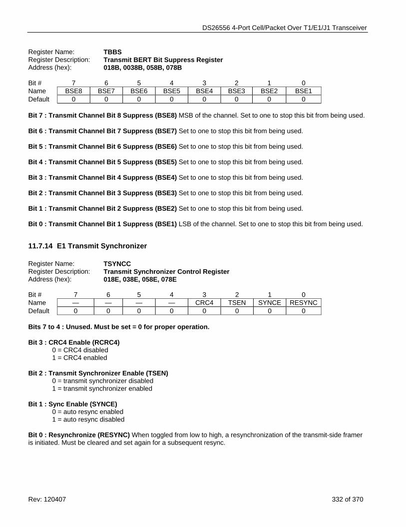
DS26556 4-Port Cell/Packet Over T1/E1/J1 Transceiver
Rev: 120407 332 of 370
Register Name: TBBS Register Description: Transmit BERT Bit Suppress Register Address (hex): 018B, 0038B, 058B, 078B Bit # 7 6 5 4 3 2 1 0 Name BSE8 BSE7 BSE6 BSE5 BSE4 BSE3 BSE2 BSE1 Default 0 0 0 0 0 0 0 0 Bit 7 : Transmit Channel Bit 8 Suppress (BSE8) MSB of the channel. Set to one to stop this bit from being used. Bit 6 : Transmit Channel Bit 7 Suppress (BSE7) Set to one to stop this bit from being used. Bit 5 : Transmit Channel Bit 6 Suppress (BSE6) Set to one to stop this bit from being used. Bit 4 : Transmit Channel Bit 5 Suppress (BSE5) Set to one to stop this bit from being used. Bit 3 : Transmit Channel Bit 4 Suppress (BSE4) Set to one to stop this bit from being used. Bit 2 : Transmit Channel Bit 3 Suppress (BSE3) Set to one to stop this bit from being used. Bit 1 : Transmit Channel Bit 2 Suppress (BSE2) Set to one to stop this bit from being used. Bit 0 : Transmit Channel Bit 1 Suppress (BSE1) LSB of the channel. Set to one to stop this bit from being used.
11.7.14 E1 Transmit Synchronizer Register Name: TSYNCC Register Description: Transmit Synchronizer Control Register Address (hex): 018E, 038E, 058E, 078E Bit # 7 6 5 4 3 2 1 0 Name — — — — CRC4 TSEN SYNCE RESYNC Default 0 0 0 0 0 0 0 0 Bits 7 to 4 : Unused. Must be set = 0 for proper operation. Bit 3 : CRC4 Enable (RCRC4)
0 = CRC4 disabled 1 = CRC4 enabled
Bit 2 : Transmit Synchronizer Enable (TSEN) 0 = transmit synchronizer disabled 1 = transmit synchronizer enabled
Bit 1 : Sync Enable (SYNCE)
0 = auto resync enabled 1 = auto resync disabled
Bit 0 : Resynchronize (RESYNC) When toggled from low to high, a resynchronization of the transmit-side framer is initiated. Must be cleared and set again for a subsequent resync.
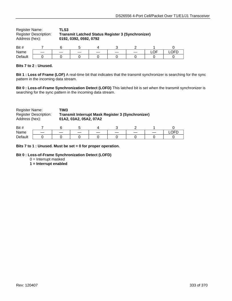
DS26556 4-Port Cell/Packet Over T1/E1/J1 Transceiver
Rev: 120407 333 of 370
Register Name: TLS3 Register Description: Transmit Latched Status Register 3 (Synchronizer) Address (hex): 0192, 0392, 0592, 0792 Bit # 7 6 5 4 3 2 1 0 Name — — — — — — LOF LOFD Default 0 0 0 0 0 0 0 0 Bits 7 to 2 : Unused. Bit 1 : Loss of Frame (LOF) A real-time bit that indicates that the transmit synchronizer is searching for the sync pattern in the incoming data stream. Bit 0 : Loss-of-Frame Synchronization Detect (LOFD) This latched bit is set when the transmit synchronizer is searching for the sync pattern in the incoming data stream. Register Name: TIM3 Register Description: Transmit Interrupt Mask Register 3 (Synchronizer) Address (hex): 01A2, 03A2, 05A2, 07A2 Bit # 7 6 5 4 3 2 1 0 Name — — — — — — — LOFD Default 0 0 0 0 0 0 0 0 Bits 7 to 1 : Unused. Must be set = 0 for proper operation. Bit 0 : Loss-of-Frame Synchronization Detect (LOFD) 0 = Interrupt masked 1 = Interrupt enabled
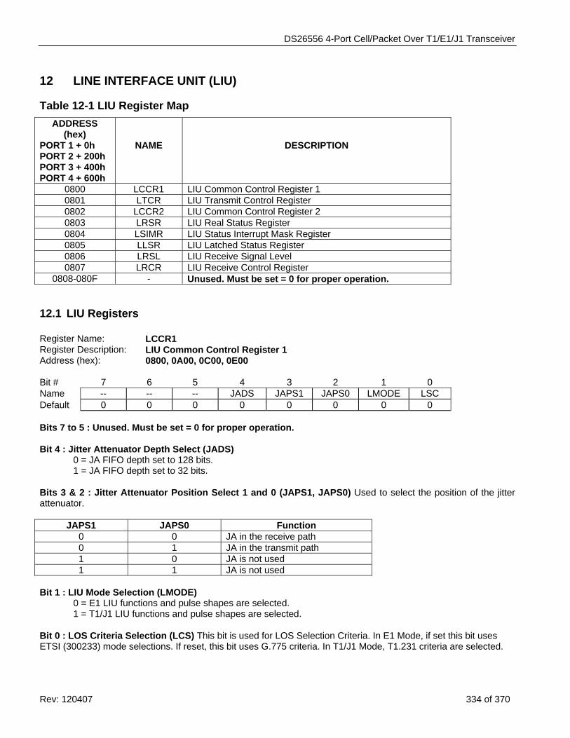
DS26556 4-Port Cell/Packet Over T1/E1/J1 Transceiver
Rev: 120407 334 of 370
12 LINE INTERFACE UNIT (LIU)
Table 12-1 LIU Register Map ADDRESS
(hex) PORT 1 + 0h PORT 2 + 200h PORT 3 + 400h PORT 4 + 600h
NAME
DESCRIPTION
0800 LCCR1 LIU Common Control Register 1 0801 LTCR LIU Transmit Control Register 0802 LCCR2 LIU Common Control Register 2 0803 LRSR LIU Real Status Register 0804 LSIMR LIU Status Interrupt Mask Register 0805 LLSR LIU Latched Status Register 0806 LRSL LIU Receive Signal Level 0807 LRCR LIU Receive Control Register
0808-080F - Unused. Must be set = 0 for proper operation.
12.1 LIU Registers Register Name: LCCR1 Register Description: LIU Common Control Register 1 Address (hex): 0800, 0A00, 0C00, 0E00 Bit # 7 6 5 4 3 2 1 0 Name -- -- -- JADS JAPS1 JAPS0 LMODE LSC Default 0 0 0 0 0 0 0 0 Bits 7 to 5 : Unused. Must be set = 0 for proper operation. Bit 4 : Jitter Attenuator Depth Select (JADS) 0 = JA FIFO depth set to 128 bits. 1 = JA FIFO depth set to 32 bits. Bits 3 & 2 : Jitter Attenuator Position Select 1 and 0 (JAPS1, JAPS0) Used to select the position of the jitter attenuator.
JAPS1 JAPS0 Function 0 0 JA in the receive path 0 1 JA in the transmit path 1 0 JA is not used 1 1 JA is not used
Bit 1 : LIU Mode Selection (LMODE)
0 = E1 LIU functions and pulse shapes are selected. 1 = T1/J1 LIU functions and pulse shapes are selected. Bit 0 : LOS Criteria Selection (LCS) This bit is used for LOS Selection Criteria. In E1 Mode, if set this bit uses ETSI (300233) mode selections. If reset, this bit uses G.775 criteria. In T1/J1 Mode, T1.231 criteria are selected.
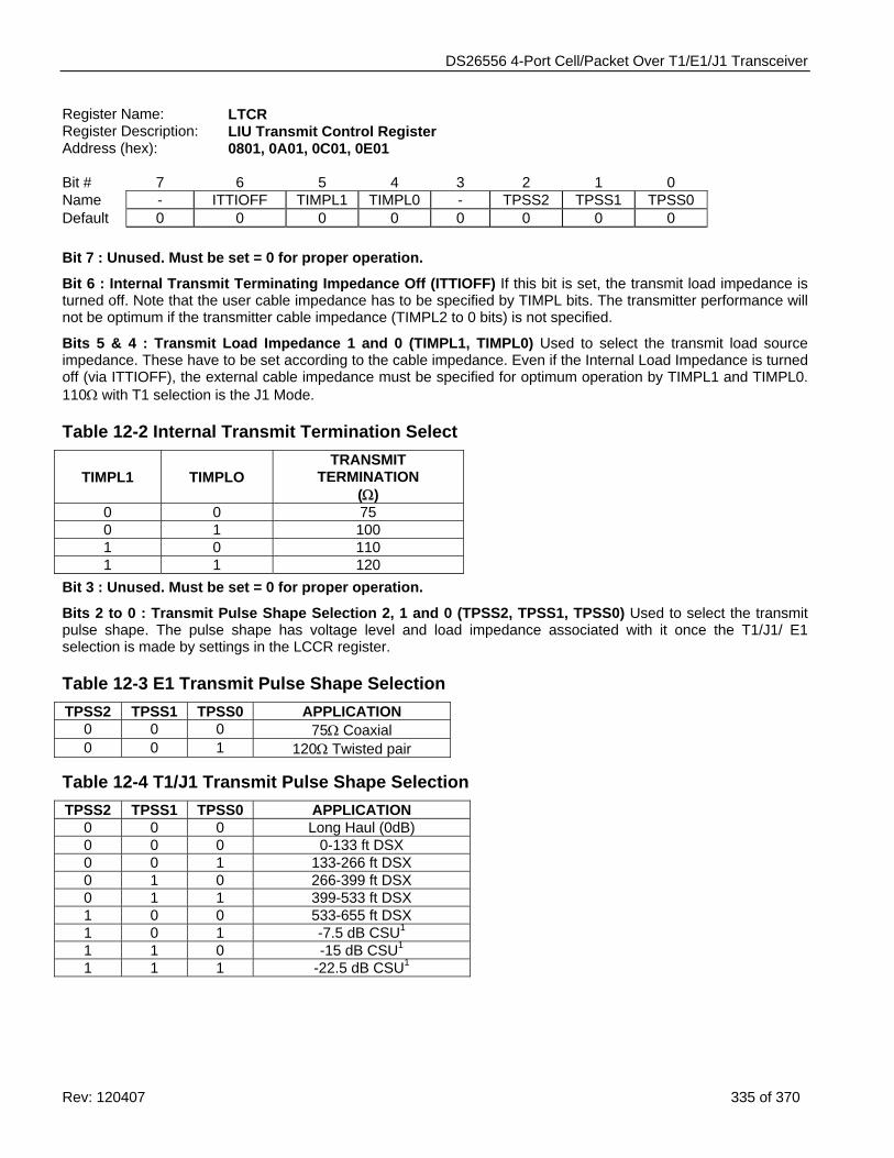
DS26556 4-Port Cell/Packet Over T1/E1/J1 Transceiver
Rev: 120407 335 of 370
Register Name: LTCR Register Description: LIU Transmit Control Register Address (hex): 0801, 0A01, 0C01, 0E01 Bit # 7 6 5 4 3 2 1 0 Name - ITTIOFF TIMPL1 TIMPL0 - TPSS2 TPSS1 TPSS0 Default 0 0 0 0 0 0 0 0 Bit 7 : Unused. Must be set = 0 for proper operation.
Bit 6 : Internal Transmit Terminating Impedance Off (ITTIOFF) If this bit is set, the transmit load impedance is turned off. Note that the user cable impedance has to be specified by TIMPL bits. The transmitter performance will not be optimum if the transmitter cable impedance (TIMPL2 to 0 bits) is not specified.
Bits 5 & 4 : Transmit Load Impedance 1 and 0 (TIMPL1, TIMPL0) Used to select the transmit load source impedance. These have to be set according to the cable impedance. Even if the Internal Load Impedance is turned off (via ITTIOFF), the external cable impedance must be specified for optimum operation by TIMPL1 and TIMPL0. 110Ω with T1 selection is the J1 Mode.
Table 12-2 Internal Transmit Termination Select
TIMPL1 TIMPLO TRANSMIT
TERMINATION (Ω)
0 0 75 0 1 100 1 0 110 1 1 120
Bit 3 : Unused. Must be set = 0 for proper operation.
Bits 2 to 0 : Transmit Pulse Shape Selection 2, 1 and 0 (TPSS2, TPSS1, TPSS0) Used to select the transmit pulse shape. The pulse shape has voltage level and load impedance associated with it once the T1/J1/ E1 selection is made by settings in the LCCR register.
Table 12-3 E1 Transmit Pulse Shape Selection TPSS2 TPSS1 TPSS0 APPLICATION
0 0 0 75Ω Coaxial 0 0 1 120Ω Twisted pair
Table 12-4 T1/J1 Transmit Pulse Shape Selection TPSS2 TPSS1 TPSS0 APPLICATION
0 0 0 Long Haul (0dB) 0 0 0 0-133 ft DSX 0 0 1 133-266 ft DSX 0 1 0 266-399 ft DSX 0 1 1 399-533 ft DSX 1 0 0 533-655 ft DSX 1 0 1 -7.5 dB CSU1 1 1 0 -15 dB CSU1 1 1 1 -22.5 dB CSU1
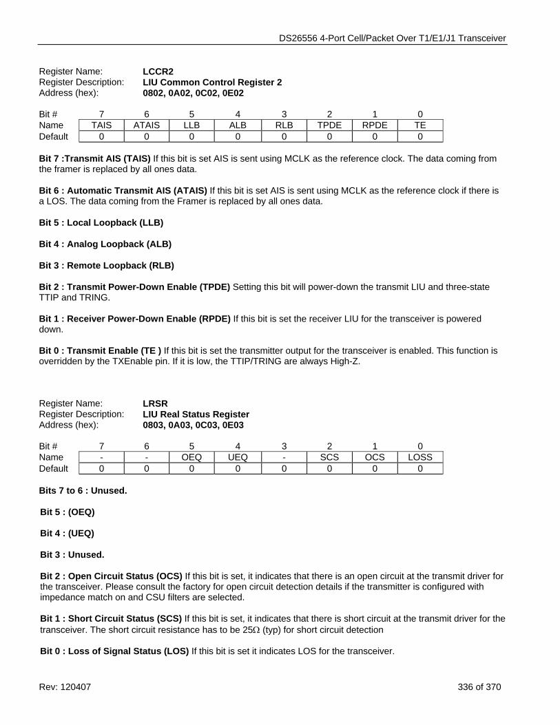
DS26556 4-Port Cell/Packet Over T1/E1/J1 Transceiver
Rev: 120407 336 of 370
Register Name: LCCR2 Register Description: LIU Common Control Register 2 Address (hex): 0802, 0A02, 0C02, 0E02 Bit # 7 6 5 4 3 2 1 0 Name TAIS ATAIS LLB ALB RLB TPDE RPDE TE Default 0 0 0 0 0 0 0 0 Bit 7 :Transmit AIS (TAIS) If this bit is set AIS is sent using MCLK as the reference clock. The data coming from the framer is replaced by all ones data. Bit 6 : Automatic Transmit AIS (ATAIS) If this bit is set AIS is sent using MCLK as the reference clock if there is a LOS. The data coming from the Framer is replaced by all ones data. Bit 5 : Local Loopback (LLB) Bit 4 : Analog Loopback (ALB) Bit 3 : Remote Loopback (RLB) Bit 2 : Transmit Power-Down Enable (TPDE) Setting this bit will power-down the transmit LIU and three-state TTIP and TRING. Bit 1 : Receiver Power-Down Enable (RPDE) If this bit is set the receiver LIU for the transceiver is powered down. Bit 0 : Transmit Enable (TE ) If this bit is set the transmitter output for the transceiver is enabled. This function is overridden by the TXEnable pin. If it is low, the TTIP/TRING are always High-Z. Register Name: LRSR Register Description: LIU Real Status Register Address (hex): 0803, 0A03, 0C03, 0E03 Bit # 7 6 5 4 3 2 1 0 Name - - OEQ UEQ - SCS OCS LOSS Default 0 0 0 0 0 0 0 0 Bits 7 to 6 : Unused. Bit 5 : (OEQ) Bit 4 : (UEQ) Bit 3 : Unused. Bit 2 : Open Circuit Status (OCS) If this bit is set, it indicates that there is an open circuit at the transmit driver for the transceiver. Please consult the factory for open circuit detection details if the transmitter is configured with impedance match on and CSU filters are selected. Bit 1 : Short Circuit Status (SCS) If this bit is set, it indicates that there is short circuit at the transmit driver for the transceiver. The short circuit resistance has to be 25Ω (typ) for short circuit detection Bit 0 : Loss of Signal Status (LOS) If this bit is set it indicates LOS for the transceiver.
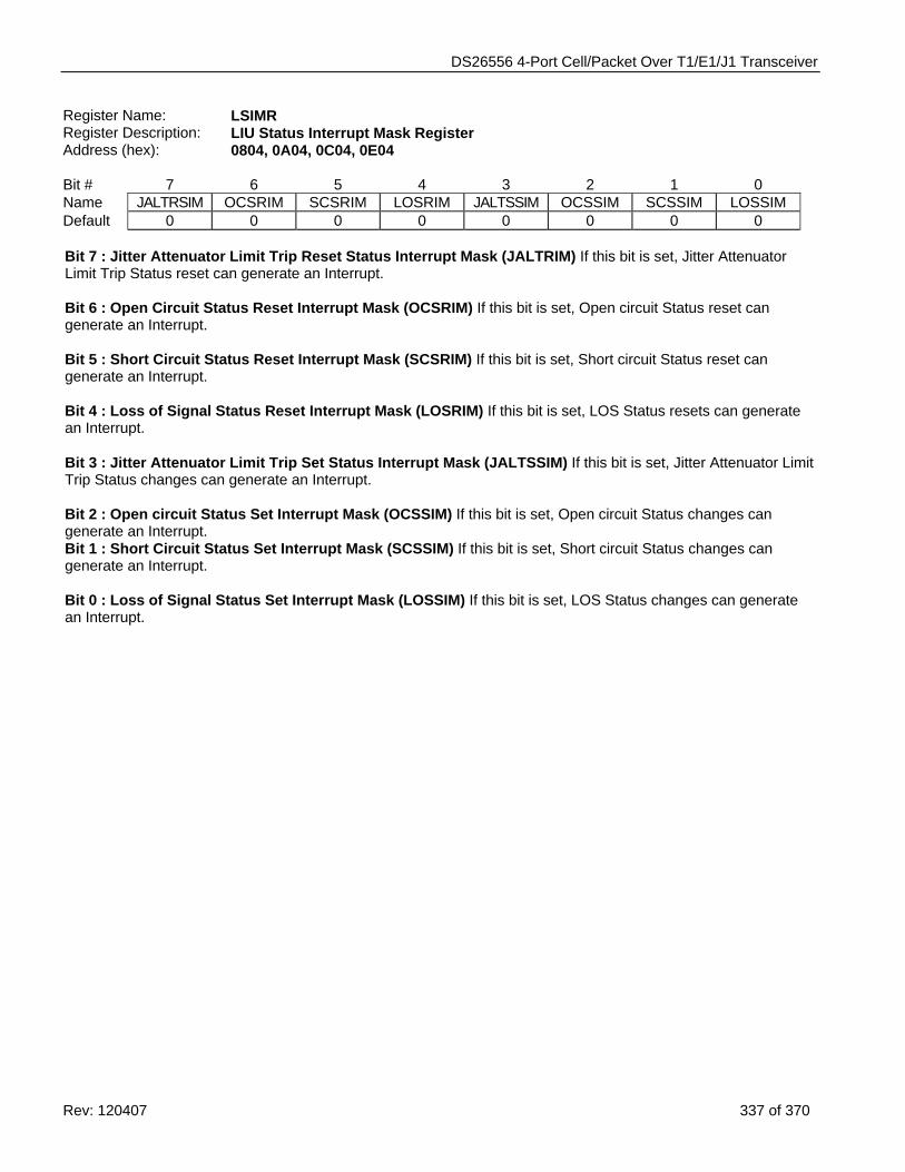
DS26556 4-Port Cell/Packet Over T1/E1/J1 Transceiver
Rev: 120407 337 of 370
Register Name: LSIMR Register Description: LIU Status Interrupt Mask Register Address (hex): 0804, 0A04, 0C04, 0E04 Bit # 7 6 5 4 3 2 1 0 Name JALTRSIM OCSRIM SCSRIM LOSRIM JALTSSIM OCSSIM SCSSIM LOSSIM Default 0 0 0 0 0 0 0 0 Bit 7 : Jitter Attenuator Limit Trip Reset Status Interrupt Mask (JALTRIM) If this bit is set, Jitter Attenuator Limit Trip Status reset can generate an Interrupt. Bit 6 : Open Circuit Status Reset Interrupt Mask (OCSRIM) If this bit is set, Open circuit Status reset can generate an Interrupt. Bit 5 : Short Circuit Status Reset Interrupt Mask (SCSRIM) If this bit is set, Short circuit Status reset can generate an Interrupt. Bit 4 : Loss of Signal Status Reset Interrupt Mask (LOSRIM) If this bit is set, LOS Status resets can generate an Interrupt. Bit 3 : Jitter Attenuator Limit Trip Set Status Interrupt Mask (JALTSSIM) If this bit is set, Jitter Attenuator Limit Trip Status changes can generate an Interrupt. Bit 2 : Open circuit Status Set Interrupt Mask (OCSSIM) If this bit is set, Open circuit Status changes can generate an Interrupt. Bit 1 : Short Circuit Status Set Interrupt Mask (SCSSIM) If this bit is set, Short circuit Status changes can generate an Interrupt. Bit 0 : Loss of Signal Status Set Interrupt Mask (LOSSIM) If this bit is set, LOS Status changes can generate an Interrupt.
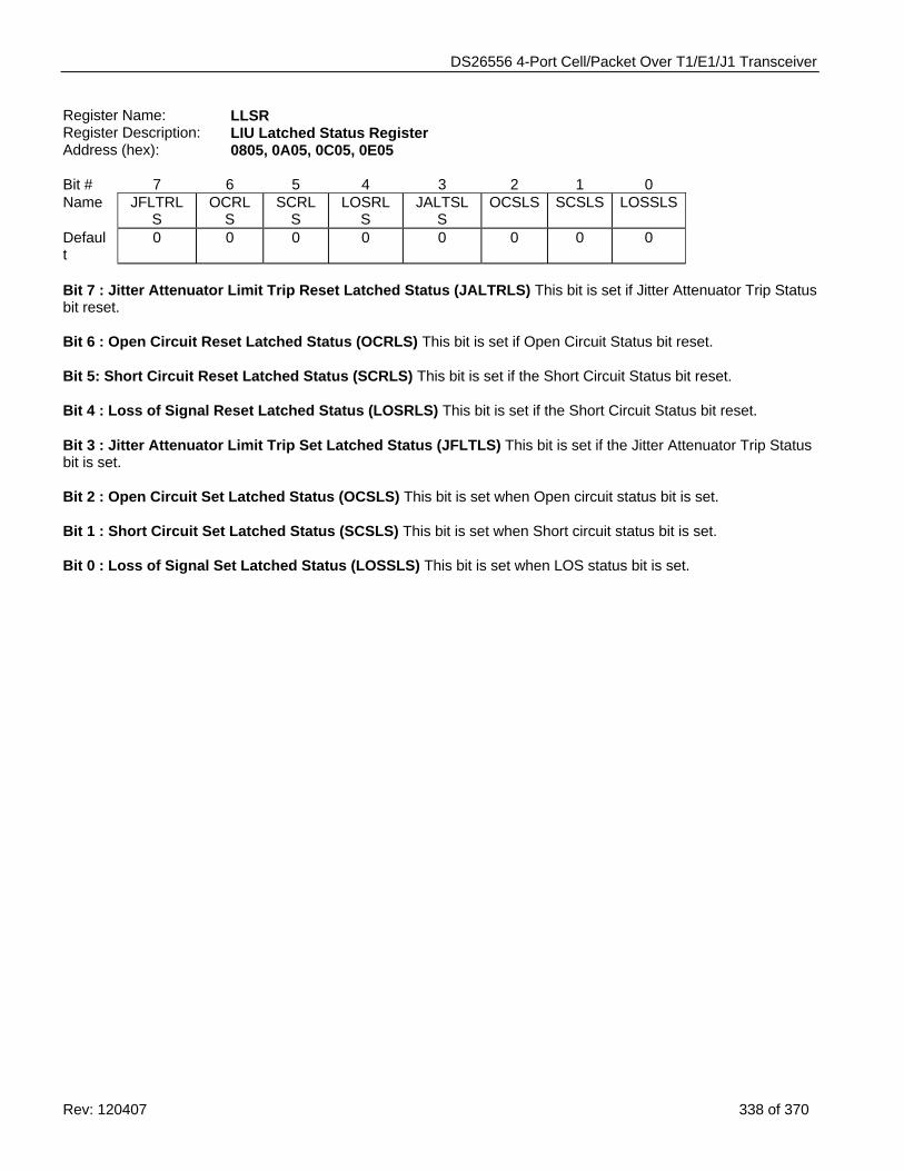
DS26556 4-Port Cell/Packet Over T1/E1/J1 Transceiver
Rev: 120407 338 of 370
Register Name: LLSR Register Description: LIU Latched Status Register Address (hex): 0805, 0A05, 0C05, 0E05 Bit # 7 6 5 4 3 2 1 0 Name JFLTRL
S OCRL
S SCRL
S LOSRL
S JALTSL
S OCSLS SCSLS LOSSLS
Default
0 0 0 0 0 0 0 0
Bit 7 : Jitter Attenuator Limit Trip Reset Latched Status (JALTRLS) This bit is set if Jitter Attenuator Trip Status bit reset. Bit 6 : Open Circuit Reset Latched Status (OCRLS) This bit is set if Open Circuit Status bit reset. Bit 5: Short Circuit Reset Latched Status (SCRLS) This bit is set if the Short Circuit Status bit reset. Bit 4 : Loss of Signal Reset Latched Status (LOSRLS) This bit is set if the Short Circuit Status bit reset. Bit 3 : Jitter Attenuator Limit Trip Set Latched Status (JFLTLS) This bit is set if the Jitter Attenuator Trip Status bit is set. Bit 2 : Open Circuit Set Latched Status (OCSLS) This bit is set when Open circuit status bit is set. Bit 1 : Short Circuit Set Latched Status (SCSLS) This bit is set when Short circuit status bit is set. Bit 0 : Loss of Signal Set Latched Status (LOSSLS) This bit is set when LOS status bit is set.
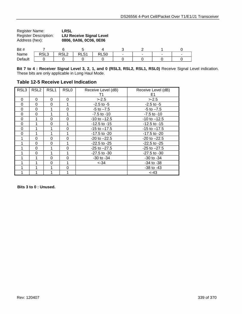
DS26556 4-Port Cell/Packet Over T1/E1/J1 Transceiver
Rev: 120407 339 of 370
Register Name: LRSL Register Description: LIU Receive Signal Level Address (hex): 0806, 0A06, 0C06, 0E06 Bit # 7 6 5 4 3 2 1 0 Name RSL3 RSL2 RLS1 RLS0 - - - - Default 0 0 0 0 0 0 0 0 Bit 7 to 4 : Receiver Signal Level 3, 2, 1, and 0 (RSL3, RSL2, RSL1, RSL0) Receive Signal Level indication. These bits are only applicable in Long Haul Mode.
Table 12-5 Receive Level Indication RSL3 RSL2 RSL1 RSL0 Receive Level (dB)
T1 Receive Level (dB)
E1 0 0 0 0 >-2.5 >-2.5 0 0 0 1 -2.5 to -5 -2.5 to -5 0 0 1 0 -5 to –7.5 -5 to –7.5 0 0 1 1 -7.5 to -10 -7.5 to -10 0 1 0 0 -10 to –12.5 -10 to –12.5 0 1 0 1 -12.5 to -15 -12.5 to -15 0 1 1 0 -15 to –17.5 -15 to –17.5 0 1 1 1 -17.5 to -20 -17.5 to -20 1 0 0 0 -20 to –22.5 -20 to –22.5 1 0 0 1 -22.5 to -25 -22.5 to -25 1 0 1 0 -25 to –27.5 -25 to –27.5 1 0 1 1 -27.5 to -30 -27.5 to -30 1 1 0 0 -30 to -34 -30 to -34 1 1 0 1 <-34 -34 to -38 1 1 1 0 -38 to -43 1 1 1 1 <-43
Bits 3 to 0 : Unused.
DS26556 4-Port Cell/Packet Over T1/E1/J1 Transceiver
Rev: 120407 340 of 370
Register Name: LRCR Register Description: LIU Receive Control Register Address (hex): 0807, 0A07, 0C07, 0E07 Bit # 7 6 5 4 3 2 1 0 Name RG703 IRTOFF IRTS1 IRTS0 RTTR RMME RSMGS1 RSMGS0 Default 0 0 0 0 0 0 0 0 Bit 7 : Receive G.703 Clock (RG703) When set = 1, the receiver expects a 2.048 MHz (E1 mode) or 1.544 MHz (T1 mode) synchronization clock (as specified by G.703) at RTIP/RRING. Bit 6 : Internal Receive Termination Off (IRTOFF) Disables the internal receive termination.
0 = internal receive termination enabled, IRTS1 and IRTS0 select termination value 1 = internal receive termination disabled. Bit 5 & 4 : Internal Receive Termination Select 1, 0 (IRTS1, IRTS0) These bits select the internal receive termination. These have to be set to match cable impedance. If the internal receive termination is disabled via IRTOFF, IRTS1 and IRTS2 should still be set to match the external cable characteristics for optimum operation.
Table 12-6 Internal Receive Termination Selection
IRTS0 IRTS1 INTERNAL RECEIVE TERMINATION (Ω)
0 0 75 0 1 100 1 0 110 1 1 120
Bit 3 : Receive Transformer Turns Ratio (RTTR) This bit is used to select receive transformer turns ratio 1:1 or 2:1 operation.
0 = 1:1 turns ratio (normal mode) 1 = 2:1 turns ratio (short haul applications only) Bit 2 : Receive Monitor Mode Enable (RMME) When set = 1, the receive monitor mode is enabled. A resistive gain will be added to the normal cable loss sensitivity. The resistive gain is determined by RSMGS1 and RSMGS0. Bits 1 & 0 : Receive Sensitivity / Monitor Gain Select 1, 0 (RSMGS1, RSMGS0) When RMME = 0, these bits are used to select the maximum receive sensitivity. When RMME = 1, these bits are used to select the receive monitor mode gain.
Table 12-7 Monitor Gain and Maximum Receive Sensitivity Selection
RMME RSMGS1 RSMGS0 MAXIMUM RECEIVE SENSITIVITY (dB)
RECEIVE MONITOR GAIN SETTINGS
0 0 0 12 0 0 0 1 20 0 0 1 0 30 0 0 1 1 36 for T1, 43 for E1 0 1 0 0 30 14 1 0 1 22.5 20 1 1 0 17.5 26 1 1 1 12 32
DS26556 4-Port Cell/Packet Over T1/E1/J1 Transceiver
Rev: 120407 341 of 370
13 BIT ERROR RATE TESTER (BERT)
Table 13-1 BERT Register Map ADDRESS
(hex) PORT 1 + 0h
PORT 2 + 200h PORT 3 + 400h PORT 4 + 600h
NAME DESCRIPTION
00E0 BCR BERT Control Register 00E1 -- Unused 00E2 BPCR1 BERT Pattern Configuration Register #1 00E3 BPCR2 BERT Pattern Configuration Register #2 00E4 BSPR1 BERT Seed/Pattern Register #1 00E5 BSPR2 BERT Seed/Pattern Register #2 00E6 BSPR3 BERT Seed/Pattern Register #3 00E7 BSPR4 BERT Seed/Pattern Register #4 00E8 TEICR Transmit Error Insertion Control Register 00E9 -- Unused 00EA -- Unused 00EB -- Unused 00EC BSR BERT Status Register 00ED -- Unused 00EE BSRL BERT Status Register Latched 00EF -- Unused 00F0 BSRIE BERT Status Register Interrupt Enable 00F1 -- Unused 00F2 -- Unused 00F3 -- Unused 00F4 RBECR1 Receive Bit Error Count Register #1 00F5 RBECR2 Receive Bit Error Count Register #2 00F6 RBECR3 Receive Bit Error Count Register #3 00F7 -- Unused 00F8 RBCR1 Receive Bit Count Register #1 00F9 RBCR2 Receive Bit Count Register #2 00FA RBCR3 Receive Bit Count Register #3 00FB RBCR4 Receive Bit Count Register #4 00FC -- Unused 00FD -- Unused 00FE -- Unused 00FF -- Unused
DS26556 4-Port Cell/Packet Over T1/E1/J1 Transceiver
Rev: 120407 342 of 370
13.1 BERT Register Bit Descriptions Register Name: BCR Register Description: BERT Control Register Register Address: E0h Bit # 7 6 5 4 3 2 1 0 Name PMUM LPMU RNPL RPIC MPR APRD TNPL TPIC Default 0 0 0 0 0 0 0 0 Bit 7/ Performance Monitoring Update Mode (PMUM) – When 0, a performance monitoring update is initiated by the LPMU register bit. When 1, a performance monitoring update is initiated by the receive performance monitoring update signal (RPMU). Note: If RPMU or LPMU is one, changing the state of this bit may cause a performance monitoring update to occur.
Bit 6/ Local Performance Monitoring Update (LPMU) – This bit causes a performance monitoring update to be initiated if local performance monitoring update is enabled (PMUM = 0). A 0 to 1 transition causes the performance monitoring registers to be updated with the latest data, and the counters reset (0 or 1). For a second performance monitoring update to be initiated, this bit must be set to 0, and back to 1. If LPMU goes low before the PMS bit goes high, an update might not be performed. This bit has no affect when PMUM=1.
Bit 5/ Receive New Pattern Load (RNPL) – A zero to one transition of this bit will cause the programmed test pattern (QRSS, PTS, PLF[4:0], PTF[4:0], and BSP[31:0]) to be loaded in to the receive pattern generator. This bit must be changed to zero and back to one for another pattern to be loaded. Loading a new pattern will forces the receive pattern generator out of the “Sync” state which causes a resynchronization to be initiated. Note: QRSS, PTS, PLF[4:0}, PTF[4:0], and BSP[31:0] must not change from the time this bit transitions from 0 to 1 until four RXCK clock cycles after this bit transitions from 0 to 1.
Bit 4/ Receive Pattern Inversion Control (RPIC) – When 0, the receive incoming data stream is not altered. When 1, the receive incoming data stream is inverted.
Bit 3/ Manual Pattern Resynchronization (MPR) – A zero to one transition of this bit will cause the receive pattern generator to resynchronize to the incoming pattern. This bit must be changed to zero and back to one for another resynchronization to be initiated. Note: A manual resynchronization forces the receive pattern generator out of the “Sync” state.
Bit 2/ Automatic Pattern Resynchronization Disable (APRD) – When 0, the receive pattern generator will automatically resynchronize to the incoming pattern if six or more times during the current 64-bit window the incoming data stream bit and the receive pattern generator output bit did not match. When 1, the receive pattern generator will not automatically resynchronize to the incoming pattern. Note: Automatic synchronization is prevented by not allowing the receive pattern generator to automatically exit the “Sync” state.
Bit 1/ Transmit New Pattern Load (TNPL) – A zero to one transition of this bit will cause the programmed test pattern (QRSS, PTS, PLF[4:0], PTF[4:0], and BSP[31:0]) to be loaded in to the transmit pattern generator. This bit must be changed to zero and back to one for another pattern to be loaded. Note: QRSS, PTS, PLF[4:0}, PTF[4:0], and BSP[31:0] must not change from the time this bit transitions from 0 to 1 until four TXCK clock cycles after this bit transitions from 0 to 1.
Bit 0/ Transmit Pattern Inversion Control (TPIC) – When 0, the transmit outgoing data stream is not altered. When 1, the transmit outgoing data stream is inverted.
DS26556 4-Port Cell/Packet Over T1/E1/J1 Transceiver
Rev: 120407 343 of 370
Register Name: BPCR1 Register Description: BERT Pattern Configuration Register #1 Register Address: E2h Bit # 7 6 5 4 3 2 1 0 Name -- QRSS PTS PLF4 PLF3 PLF2 PLF1 PLF0 Default 0 0 0 0 0 0 0 0 Bit 6/ QRSS Enable (QRSS) – When 0, the pattern generator configuration is controlled by PTS, PLF[4:0], and PTF[4:0], and BSP[31:0]. When 1, the pattern generator configuration is forced to a PRBS pattern with a generating polynomial of x20 + x17 + 1. The output of the pattern generator will be forced to one if the next fourteen output bits are all zero.
Bit 5/ Pattern Type Select (PTS) – When 0, the pattern is a PRBS pattern. When 1, the pattern is a repetitive pattern.
Bit 4-0/ Pattern Length Feedback (PLF[4:0]) – These five bits control the “length” feedback of the pattern generator. The “length” feedback will be from bit n of the pattern generator (n = PLF[4:0] +1). For a PRBS signal, the feedback is an XOR of bit n and bit y. For a repetitive pattern the feedback is bit n. Register Name: BPCR2 Register Description: BERT Pattern Configuration Register #2 Register Address: E3h Bit # 7 6 5 4 3 2 1 0 Name -- -- -- PTF4 PTF3 PTF2 PTF1 PTF0 Default 0 0 0 0 0 0 0 0 Bits 4 to 0: Pattern Tap Feedback (PTF[4:0]) – These five bits control the PRBS “tap” feedback of the pattern generator. The “tap” feedback will be from bit y of the pattern generator (y = PTF[4:0] +1). These bits are ignored when programmed for a repetitive pattern. For a PRBS signal, the feedback is an XOR of bit n and bit y.
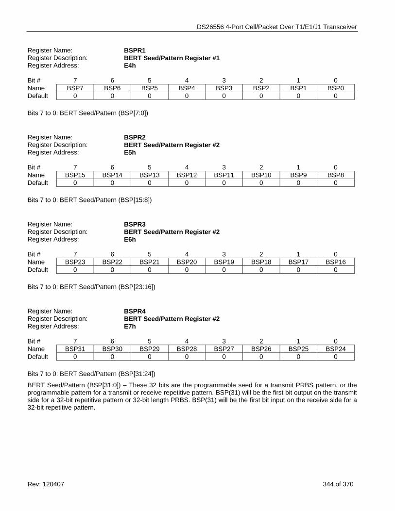
DS26556 4-Port Cell/Packet Over T1/E1/J1 Transceiver
Rev: 120407 344 of 370
Register Name: BSPR1 Register Description: BERT Seed/Pattern Register #1 Register Address: E4h Bit # 7 6 5 4 3 2 1 0 Name BSP7 BSP6 BSP5 BSP4 BSP3 BSP2 BSP1 BSP0 Default 0 0 0 0 0 0 0 0 Bits 7 to 0: BERT Seed/Pattern (BSP[7:0]) Register Name: BSPR2 Register Description: BERT Seed/Pattern Register #2 Register Address: E5h Bit # 7 6 5 4 3 2 1 0 Name BSP15 BSP14 BSP13 BSP12 BSP11 BSP10 BSP9 BSP8 Default 0 0 0 0 0 0 0 0 Bits 7 to 0: BERT Seed/Pattern (BSP[15:8]) Register Name: BSPR3 Register Description: BERT Seed/Pattern Register #2 Register Address: E6h Bit # 7 6 5 4 3 2 1 0 Name BSP23 BSP22 BSP21 BSP20 BSP19 BSP18 BSP17 BSP16 Default 0 0 0 0 0 0 0 0 Bits 7 to 0: BERT Seed/Pattern (BSP[23:16]) Register Name: BSPR4 Register Description: BERT Seed/Pattern Register #2 Register Address: E7h Bit # 7 6 5 4 3 2 1 0 Name BSP31 BSP30 BSP29 BSP28 BSP27 BSP26 BSP25 BSP24 Default 0 0 0 0 0 0 0 0 Bits 7 to 0: BERT Seed/Pattern (BSP[31:24])
BERT Seed/Pattern (BSP[31:0]) – These 32 bits are the programmable seed for a transmit PRBS pattern, or the programmable pattern for a transmit or receive repetitive pattern. BSP(31) will be the first bit output on the transmit side for a 32-bit repetitive pattern or 32-bit length PRBS. BSP(31) will be the first bit input on the receive side for a 32-bit repetitive pattern.
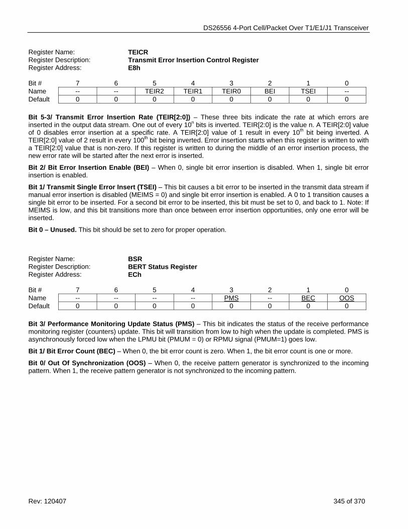
DS26556 4-Port Cell/Packet Over T1/E1/J1 Transceiver
Rev: 120407 345 of 370
Register Name: TEICR Register Description: Transmit Error Insertion Control Register Register Address: E8h Bit # 7 6 5 4 3 2 1 0 Name -- -- TEIR2 TEIR1 TEIR0 BEI TSEI -- Default 0 0 0 0 0 0 0 0 Bit 5-3/ Transmit Error Insertion Rate (TEIR[2:0]) – These three bits indicate the rate at which errors are inserted in the output data stream. One out of every 10n bits is inverted. TEIR[2:0] is the value n. A TEIR[2:0] value of 0 disables error insertion at a specific rate. A TEIR[2:0] value of 1 result in every 10th bit being inverted. A TEIR[2:0] value of 2 result in every 100th bit being inverted. Error insertion starts when this register is written to with a TEIR[2:0] value that is non-zero. If this register is written to during the middle of an error insertion process, the new error rate will be started after the next error is inserted.
Bit 2/ Bit Error Insertion Enable (BEI) – When 0, single bit error insertion is disabled. When 1, single bit error insertion is enabled.
Bit 1/ Transmit Single Error Insert (TSEI) – This bit causes a bit error to be inserted in the transmit data stream if manual error insertion is disabled (MEIMS = 0) and single bit error insertion is enabled. A 0 to 1 transition causes a single bit error to be inserted. For a second bit error to be inserted, this bit must be set to 0, and back to 1. Note: If MEIMS is low, and this bit transitions more than once between error insertion opportunities, only one error will be inserted.
Bit 0 – Unused. This bit should be set to zero for proper operation.
Register Name: BSR Register Description: BERT Status Register Register Address: ECh Bit # 7 6 5 4 3 2 1 0 Name -- -- -- -- PMS -- BEC OOS Default 0 0 0 0 0 0 0 0 Bit 3/ Performance Monitoring Update Status (PMS) – This bit indicates the status of the receive performance monitoring register (counters) update. This bit will transition from low to high when the update is completed. PMS is asynchronously forced low when the LPMU bit (PMUM = 0) or RPMU signal (PMUM=1) goes low.
Bit 1/ Bit Error Count (BEC) – When 0, the bit error count is zero. When 1, the bit error count is one or more.
Bit 0/ Out Of Synchronization (OOS) – When 0, the receive pattern generator is synchronized to the incoming pattern. When 1, the receive pattern generator is not synchronized to the incoming pattern.
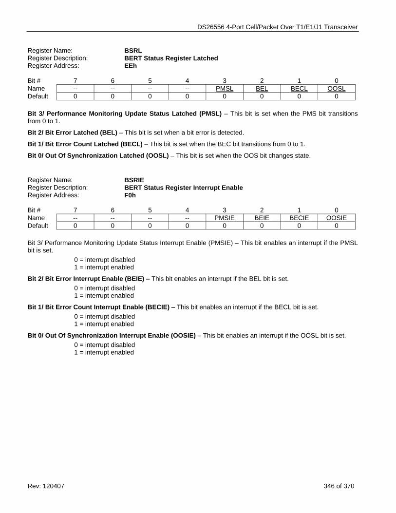
DS26556 4-Port Cell/Packet Over T1/E1/J1 Transceiver
Rev: 120407 346 of 370
Register Name: BSRL Register Description: BERT Status Register Latched Register Address: EEh Bit # 7 6 5 4 3 2 1 0 Name -- -- -- -- PMSL BEL BECL OOSL Default 0 0 0 0 0 0 0 0 Bit 3/ Performance Monitoring Update Status Latched (PMSL) – This bit is set when the PMS bit transitions from 0 to 1.
Bit 2/ Bit Error Latched (BEL) – This bit is set when a bit error is detected.
Bit 1/ Bit Error Count Latched (BECL) – This bit is set when the BEC bit transitions from 0 to 1.
Bit 0/ Out Of Synchronization Latched (OOSL) – This bit is set when the OOS bit changes state. Register Name: BSRIE Register Description: BERT Status Register Interrupt Enable Register Address: F0h Bit # 7 6 5 4 3 2 1 0 Name -- -- -- -- PMSIE BEIE BECIE OOSIE Default 0 0 0 0 0 0 0 0 Bit 3/ Performance Monitoring Update Status Interrupt Enable (PMSIE) – This bit enables an interrupt if the PMSL bit is set.
0 = interrupt disabled 1 = interrupt enabled
Bit 2/ Bit Error Interrupt Enable (BEIE) – This bit enables an interrupt if the BEL bit is set. 0 = interrupt disabled 1 = interrupt enabled
Bit 1/ Bit Error Count Interrupt Enable (BECIE) – This bit enables an interrupt if the BECL bit is set. 0 = interrupt disabled 1 = interrupt enabled
Bit 0/ Out Of Synchronization Interrupt Enable (OOSIE) – This bit enables an interrupt if the OOSL bit is set. 0 = interrupt disabled 1 = interrupt enabled
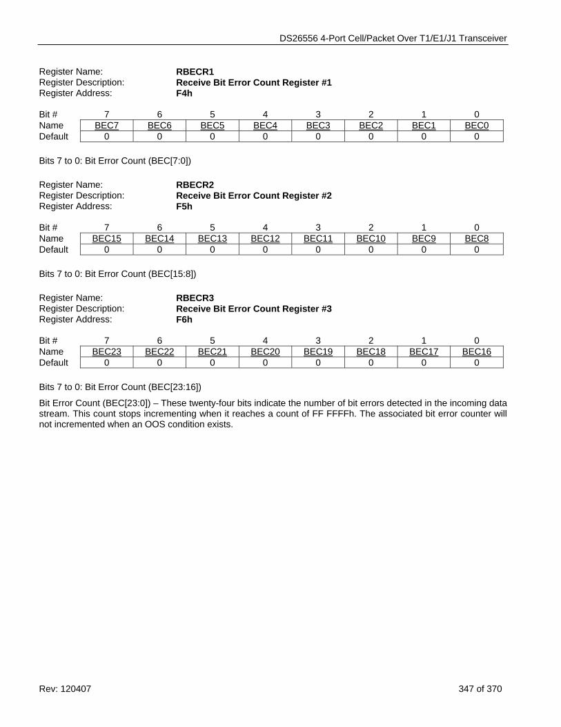
DS26556 4-Port Cell/Packet Over T1/E1/J1 Transceiver
Rev: 120407 347 of 370
Register Name: RBECR1 Register Description: Receive Bit Error Count Register #1 Register Address: F4h Bit # 7 6 5 4 3 2 1 0 Name BEC7 BEC6 BEC5 BEC4 BEC3 BEC2 BEC1 BEC0 Default 0 0 0 0 0 0 0 0 Bits 7 to 0: Bit Error Count (BEC[7:0]) Register Name: RBECR2 Register Description: Receive Bit Error Count Register #2 Register Address: F5h Bit # 7 6 5 4 3 2 1 0 Name BEC15 BEC14 BEC13 BEC12 BEC11 BEC10 BEC9 BEC8 Default 0 0 0 0 0 0 0 0 Bits 7 to 0: Bit Error Count (BEC[15:8]) Register Name: RBECR3 Register Description: Receive Bit Error Count Register #3 Register Address: F6h Bit # 7 6 5 4 3 2 1 0 Name BEC23 BEC22 BEC21 BEC20 BEC19 BEC18 BEC17 BEC16 Default 0 0 0 0 0 0 0 0 Bits 7 to 0: Bit Error Count (BEC[23:16])
Bit Error Count (BEC[23:0]) – These twenty-four bits indicate the number of bit errors detected in the incoming data stream. This count stops incrementing when it reaches a count of FF FFFFh. The associated bit error counter will not incremented when an OOS condition exists.
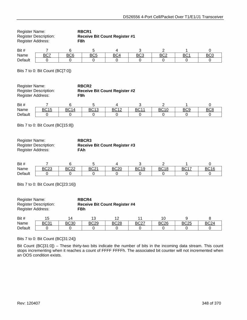
DS26556 4-Port Cell/Packet Over T1/E1/J1 Transceiver
Rev: 120407 348 of 370
Register Name: RBCR1 Register Description: Receive Bit Count Register #1 Register Address: F8h Bit # 7 6 5 4 3 2 1 0 Name BC7 BC6 BC5 BC4 BC3 BC2 BC1 BC0 Default 0 0 0 0 0 0 0 0 Bits 7 to 0: Bit Count (BC[7:0]) Register Name: RBCR2 Register Description: Receive Bit Count Register #2 Register Address: F9h Bit # 7 6 5 4 3 2 1 0 Name BC15 BC14 BC13 BC12 BC11 BC10 BC9 BC8 Default 0 0 0 0 0 0 0 0 Bits 7 to 0: Bit Count (BC[15:8]) Register Name: RBCR3 Register Description: Receive Bit Count Register #3 Register Address: FAh Bit # 7 6 5 4 3 2 1 0 Name BC23 BC22 BC21 BC20 BC19 BC18 BC17 BC16 Default 0 0 0 0 0 0 0 0 Bits 7 to 0: Bit Count (BC[23:16]) Register Name: RBCR4 Register Description: Receive Bit Count Register #4 Register Address: FBh Bit # 15 14 13 12 11 10 9 8 Name BC31 BC30 BC29 BC28 BC27 BC26 BC25 BC24 Default 0 0 0 0 0 0 0 0 Bits 7 to 0: Bit Count (BC[31:24])
Bit Count (BC[31:0]) – These thirty-two bits indicate the number of bits in the incoming data stream. This count stops incrementing when it reaches a count of FFFF FFFFh. The associated bit counter will not incremented when an OOS condition exists.
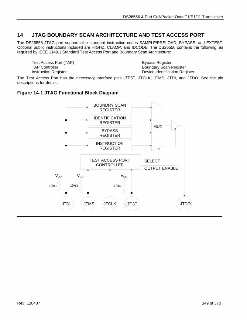
DS26556 4-Port Cell/Packet Over T1/E1/J1 Transceiver
Rev: 120407 349 of 370
14 JTAG BOUNDARY SCAN ARCHITECTURE AND TEST ACCESS PORT The DS26556 JTAG port supports the standard instruction codes SAMPLE/PRELOAD, BYPASS, and EXTEST. Optional public instructions included are HIGHZ, CLAMP, and IDCODE. The DS26556 contains the following, as required by IEEE 1149.1 Standard Test Access Port and Boundary Scan Architecture:
Test Access Port (TAP) TAP Controller Instruction Register
Bypass Register Boundary Scan Register Device Identification Register
The Test Access Port has the necessary interface pins JTRST, JTCLK, JTMS, JTDI, and JTDO. See the pin descriptions for details.
Figure 14-1 JTAG Functional Block Diagram
JTDI JTMS JTCLK JTRST JTDO
TEST ACCESS PORT CONTROLLER
VDD VDD VDD
BOUNDRY SCAN REGISTER
BYPASS REGISTER
INSTRUCTION REGISTER
IDENTIFICATION REGISTER
MUX
SELECT
OUTPUT ENABLE
10kΩ 10kΩ 10kΩ
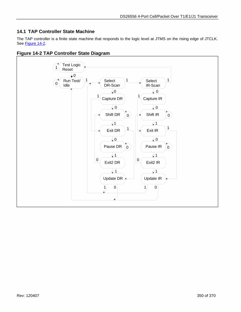
DS26556 4-Port Cell/Packet Over T1/E1/J1 Transceiver
Rev: 120407 350 of 370
14.1 TAP Controller State Machine The TAP controller is a finite state machine that responds to the logic level at JTMS on the rising edge of JTCLK. See Figure 14-2.
Figure 14-2 TAP Controller State Diagram
1
0
01
1 1
1
1
1
11
1 1
110 0
0 0
0
1
0 0
00
1 1
00
0 0
SelectDR-Scan
Capture DR
Shift DR
Exit DR
Pause DR
Exit2 DR
Update DR
SelectIR-Scan
Capture IR
Shift IR
Exit IR
Pause IR
Exit2 IR
Update IR
Test LogicReset
Run Test/Idle
0
DS26556 4-Port Cell/Packet Over T1/E1/J1 Transceiver
Rev: 120407 351 of 370
14.1.1 Test-Logic-Reset Upon power-up, the TAP Controller will be in the Test-Logic-Reset state. The Instruction register will contain the IDCODE instruction. All system logic of the device will operate normally.
14.1.2 Run-Test-Idle The Run-Test-Idle is used between scan operations or during specific tests. The Instruction register and test registers will remain idle.
14.1.3 Select-DR-Scan All test registers retain their previous state. With JTMS LOW, a rising edge of JTCLK moves the controller into the Capture-DR state and will initiate a scan sequence. JTMS HIGH during a rising edge on JTCLK moves the controller to the Select-IR-Scan state.
14.1.4 Capture-DR Data may be parallel-loaded into the test data registers selected by the current instruction. If the instruction does not call for a parallel load or the selected register does not allow parallel loads, the test register will remain at its current value. On the rising edge of JTCLK, the controller will go to the Shift-DR state if JTMS is LOW or it will go to the Exit1-DR state if JTMS is HIGH.
14.1.5 Shift-DR The test data register selected by the current instruction will be connected between JTDI and JTDO and will shift data one stage towards its serial output on each rising edge of JTCLK. If a test register selected by the current instruction is not placed in the serial path, it will maintain its previous state.
14.1.6 Exit1-DR While in this state, a rising edge on JTCLK will put the controller in the Update-DR state, which terminates the scanning process, if JTMS is HIGH. A rising edge on JTCLK with JTMS LOW will put the controller in the Pause-DR state.
14.1.7 Pause-DR Shifting of the test registers is halted while in this state. All test registers selected by the current instruction will retain their previous state. The controller will remain in this state while JTMS is LOW. A rising edge on JTCLK with JTMS HIGH will put the controller in the Exit2-DR state.
14.1.8 Exit2-DR A rising edge on JTCLK with JTMS HIGH while in this state will put the controller in the Update-DR state and terminate the scanning process. A rising edge on JTCLK with JTMS LOW will enter the Shift-DR state.
14.1.9 Update-DR A falling edge on JTCLK while in the Update-DR state will latch the data from the shift register path of the test registers into the data output latches. This prevents changes at the parallel output due to changes in the shift register.
14.1.10 Select-IR-Scan All test registers retain their previous state. The instruction register will remain unchanged during this state. With JTMS LOW, a rising edge on JTCLK moves the controller into the Capture-IR state and will initiate a scan sequence for the instruction register. JTMS HIGH during a rising edge on JTCLK puts the controller back into the Test-Logic-Reset state.
DS26556 4-Port Cell/Packet Over T1/E1/J1 Transceiver
Rev: 120407 352 of 370
14.1.11 Capture-IR The Capture-IR state is used to load the shift register in the instruction register with a fixed value. This value is loaded on the rising edge of JTCLK. If JTMS is HIGH on the rising edge of JTCLK, the controller will enter the Exit1-IR state. If JTMS is LOW on the rising edge of JTCLK, the controller will enter the Shift-IR state.
14.1.12 Shift-IR In this state, the shift register in the instruction register is connected between JTDI and JTDO and shifts data one stage for every rising edge of JTCLK towards the serial output. The parallel register and all test registers remain at their previous states. A rising edge on JTCLK with JTMS HIGH will move the controller to the Exit1-IR state. A rising edge on JTCLK with JTMS LOW will keep the controller in the Shift-IR state while moving data one stage thorough the instruction shift register.
14.1.13 Exit1-IR A rising edge on JTCLK with JTMS LOW will put the controller in the Pause-IR state. If JTMS is HIGH on the rising edge of JTCLK, the controller will enter the Update-IR state and terminate the scanning process.
14.1.14 Pause-IR Shifting of the instruction shift register is halted temporarily. With JTMS HIGH, a rising edge on JTCLK will put the controller in the Exit2-IR state. The controller will remain in the Pause-IR state if JTMS is LOW during a rising edge on JTCLK.
14.1.15 Exit2-IR A rising edge on JTCLK with JTMS LOW will put the controller in the Update-IR state. The controller will loop back to Shift-IR if JTMS is HIGH during a rising edge of JTCLK in this state.
14.1.16 Update-IR The instruction code shifted into the instruction shift register is latched into the parallel output on the falling edge of JTCLK as the controller enters this state. Once latched, this instruction becomes the current instruction. A rising edge on JTCLK with JTMS LOW puts the controller in the Run-Test-Idle state. With JTMS HIGH, the controller enters the Select-DR-Scan state.
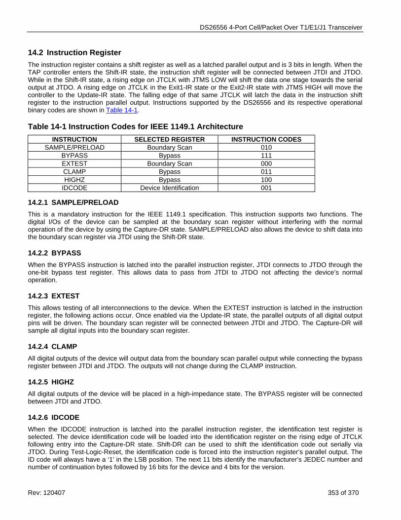
DS26556 4-Port Cell/Packet Over T1/E1/J1 Transceiver
Rev: 120407 353 of 370
14.2 Instruction Register The instruction register contains a shift register as well as a latched parallel output and is 3 bits in length. When the TAP controller enters the Shift-IR state, the instruction shift register will be connected between JTDI and JTDO. While in the Shift-IR state, a rising edge on JTCLK with JTMS LOW will shift the data one stage towards the serial output at JTDO. A rising edge on JTCLK in the Exit1-IR state or the Exit2-IR state with JTMS HIGH will move the controller to the Update-IR state. The falling edge of that same JTCLK will latch the data in the instruction shift register to the instruction parallel output. Instructions supported by the DS26556 and its respective operational binary codes are shown in Table 14-1.
Table 14-1 Instruction Codes for IEEE 1149.1 Architecture INSTRUCTION SELECTED REGISTER INSTRUCTION CODES
SAMPLE/PRELOAD Boundary Scan 010 BYPASS Bypass 111 EXTEST Boundary Scan 000 CLAMP Bypass 011 HIGHZ Bypass 100
IDCODE Device Identification 001
14.2.1 SAMPLE/PRELOAD This is a mandatory instruction for the IEEE 1149.1 specification. This instruction supports two functions. The digital I/Os of the device can be sampled at the boundary scan register without interfering with the normal operation of the device by using the Capture-DR state. SAMPLE/PRELOAD also allows the device to shift data into the boundary scan register via JTDI using the Shift-DR state.
14.2.2 BYPASS When the BYPASS instruction is latched into the parallel instruction register, JTDI connects to JTDO through the one-bit bypass test register. This allows data to pass from JTDI to JTDO not affecting the device’s normal operation.
14.2.3 EXTEST This allows testing of all interconnections to the device. When the EXTEST instruction is latched in the instruction register, the following actions occur. Once enabled via the Update-IR state, the parallel outputs of all digital output pins will be driven. The boundary scan register will be connected between JTDI and JTDO. The Capture-DR will sample all digital inputs into the boundary scan register.
14.2.4 CLAMP All digital outputs of the device will output data from the boundary scan parallel output while connecting the bypass register between JTDI and JTDO. The outputs will not change during the CLAMP instruction.
14.2.5 HIGHZ All digital outputs of the device will be placed in a high-impedance state. The BYPASS register will be connected between JTDI and JTDO.
14.2.6 IDCODE When the IDCODE instruction is latched into the parallel instruction register, the identification test register is selected. The device identification code will be loaded into the identification register on the rising edge of JTCLK following entry into the Capture-DR state. Shift-DR can be used to shift the identification code out serially via JTDO. During Test-Logic-Reset, the identification code is forced into the instruction register’s parallel output. The ID code will always have a ‘1’ in the LSB position. The next 11 bits identify the manufacturer’s JEDEC number and number of continuation bytes followed by 16 bits for the device and 4 bits for the version.
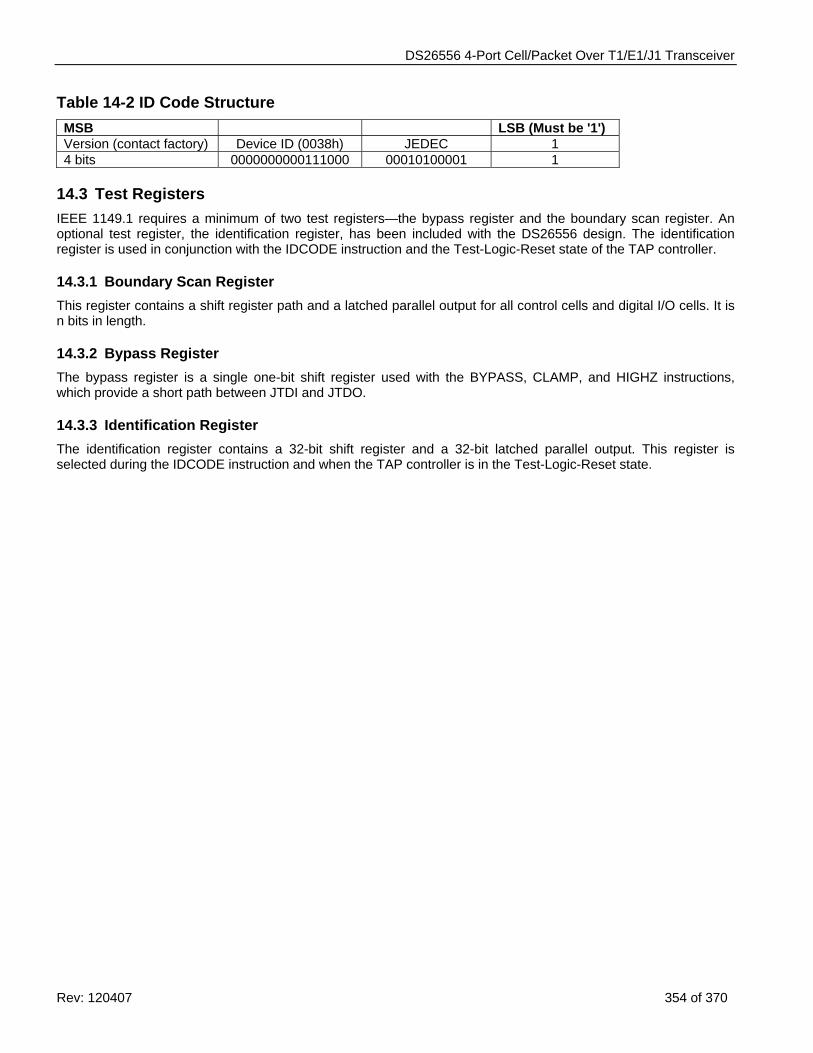
DS26556 4-Port Cell/Packet Over T1/E1/J1 Transceiver
Rev: 120407 354 of 370
Table 14-2 ID Code Structure MSB LSB (Must be '1') Version (contact factory) Device ID (0038h) JEDEC 1 4 bits 0000000000111000 00010100001 1
14.3 Test Registers IEEE 1149.1 requires a minimum of two test registers—the bypass register and the boundary scan register. An optional test register, the identification register, has been included with the DS26556 design. The identification register is used in conjunction with the IDCODE instruction and the Test-Logic-Reset state of the TAP controller.
14.3.1 Boundary Scan Register This register contains a shift register path and a latched parallel output for all control cells and digital I/O cells. It is n bits in length.
14.3.2 Bypass Register The bypass register is a single one-bit shift register used with the BYPASS, CLAMP, and HIGHZ instructions, which provide a short path between JTDI and JTDO.
14.3.3 Identification Register The identification register contains a 32-bit shift register and a 32-bit latched parallel output. This register is selected during the IDCODE instruction and when the TAP controller is in the Test-Logic-Reset state.
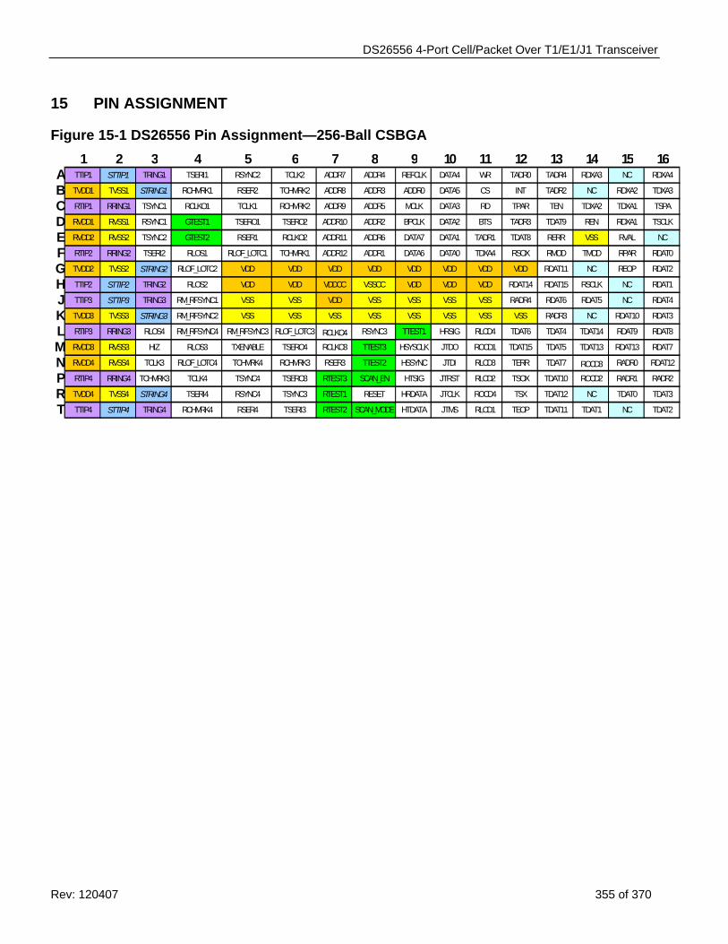
DS26556 4-Port Cell/Packet Over T1/E1/J1 Transceiver
Rev: 120407 355 of 370
15 PIN ASSIGNMENT
Figure 15-1 DS26556 Pin Assignment—256-Ball CSBGA 1 2 3 4 5 6 7 8 9 10 11 12 13 14 15 16
A TTIP1 STTIP1 TRING1 TSERI1 RSYNC2 TCLK2 ADDR7 ADDR4 REFCLK DATA4 WR TADR0 TADR4 RDXA3 NC RDXA4
B TVDD1 TVSS1 STRING1 RCHMRK1 RSER2 TCHMRK2 ADDR8 ADDR3 ADDR0 DATA5 CS INT TADR2 NC RDXA2 TDXA3
C RTIP1 RRING1 TSYNC1 RCLKO1 TCLK1 RCHMRK2 ADDR9 ADDR5 MCLK DATA3 RD TPAR TEN TDXA2 TDXA1 TSPA
D RVDD1 RVSS1 RSYNC1 GTEST1 TSERO1 TSERO2 ADDR10 ADDR2 BPCLK DATA2 BTS TADR3 TDAT9 REN RDXA1 TSCLK
E RVDD2 RVSS2 TSYNC2 GTEST2 RSER1 RCLKO2 ADDR11 ADDR6 DATA7 DATA1 TADR1 TDAT8 RERR VSS RVAL NC
F RTIP2 RRING2 TSERI2 RLOS1 RLOF_LOTC1 TCHMRK1 ADDR12 ADDR1 DATA6 DATA0 TDXA4 RSOX RMOD TMOD RPAR RDAT0
G TVDD2 TVSS2 STRING2 RLOF_LOTC2 VDD VDD VDD VDD VDD VDD VDD VDD RDAT11 NC REOP RDAT2
H TTIP2 STTIP2 TRING2 RLOS2 VDD VDD VDDCC VSSCC VDD VDD VDD RDAT14 RDAT15 RSCLK NC RDAT1
J TTIP3 STTIP3 TRING3 RM_RFSYNC1 VSS VSS VDD VSS VSS VSS VSS RADR4 RDAT6 RDAT5 NC RDAT4
K TVDD3 TVSS3 STRING3 RM_RFSYNC2 VSS VSS VSS VSS VSS VSS VSS VSS RADR3 NC RDAT10 RDAT3
L RTIP3 RRING3 RLOS4 RM_RFSYNC4 RM_RFSYNC3 RLOF_LOTC3 RCLKO4 RSYNC3 TTEST1 HRSIG RLCD4 TDAT6 TDAT4 TDAT14 RDAT9 RDAT8
M RVDD3 RVSS3 HIZ RLOS3 TXENABLE TSERO4 RCLKO3 TTEST3 HSYSCLK JTDO ROCD1 TDAT15 TDAT5 TDAT13 RDAT13 RDAT7
N RVDD4 RVSS4 TCLK3 RLOF_LOTC4 TCHMRK4 RCHMRK3 RSER3 TTEST2 HSSYNC JTDI RLCD3 TERR TDAT7 ROCD3 RADR0 RDAT12
P RTIP4 RRING4 TCHMRK3 TCLK4 TSYNC4 TSERO3 RTEST3 SCAN_EN HTSIG JTRST RLCD2 TSOX TDAT10 ROCD2 RADR1 RADR2
R TVDD4 TVSS4 STRING4 TSERI4 RSYNC4 TSYNC3 RTEST1 RESET HRDATA JTCLK ROCD4 TSX TDAT12 NC TDAT0 TDAT3
T TTIP4 STTIP4 TRING4 RCHMRK4 RSER4 TSERI3 RTEST2 SCAN_MODE HTDATA JTMS RLCD1 TEOP TDAT11 TDAT1 NC TDAT2
DS26556 4-Port Cell/Packet Over T1/E1/J1 Transceiver
Rev: 120407 356 of 370
16 PACKAGE INFORMATION (The package drawing(s) in this data sheet may not reflect the most current specifications. The package number provided for each package is a link to the latest package outline information.)
16.1 256-Ball TE-CSBGA (56-G6028-001)
DS26556 4-Port Cell/Packet Over T1/E1/J1 Transceiver
Rev: 120407 357 of 370
17 THERMAL INFORMATION
Table 17-1 Thermal Characteristics
PARAMETER MIN TYP MAX UNITS
Ambient Temperature (Note 1) -40 +85 °C Junction Temperature +125 °C Theta-JA (θJA) in Still Air for 17mm CSBGA (Note 2) +17.5 °C/W
Note 1: The package is mounted on a four-layer JEDEC standard test board.
Note 2: Theta-JA (θJA) is the junction-to-ambient thermal resistance, when the package is mounted on a four-layer JEDEC standard test board.
DS26556 4-Port Cell/Packet Over T1/E1/J1 Transceiver
Rev: 120407 358 of 370
18 ABSOLUTE MAXIMUM RATINGS
Table 18-1 Absolute Maximum Ratings Voltage Range on Any Pin Relative to Ground -1.0V to +6.0V Operating Temperature Range for DS26556 0°C to +70°C Operating Temperature Range for DS26556N -40°C to +85°C (Note 1) Storage Temperature Range -55°C to +125°C Soldering Temperature See IPC/JEDEC J-STD-020 Standard This is a stress rating only and functional operation of the device at these or any other conditions above those indicated in the operation sections of this specification is not implied. Exposure to absolute maximum rating conditions for extended periods of time can affect reliability. Note 1: Specifications to -40°C are guaranteedy by design (GBD) and not production tested.
Table 18-2 Recommended DC Operating Conditions (TA = 0°C to +70°C for DS26556; TA = -40°C to +85°C for DS26556N.)
PARAMETER SYMBOL CONDITIONS MIN TYP MAX UNITS Logic 1 VIH 2.0 5.5 V Logic 0 VIL -0.3 +0.8 V Supply VDD (Note 2) 3.135 3.3 3.465 V
Table 18-3 Capacitance (TA = +25°C)
PARAMETER SYMBOL CONDITIONS MIN TYP MAX UNITS Input Capacitance CIN 5 pF Output Capacitance COUT 7 pF
Table 18-4 DC Operating Characteristics (VDD = 3.3V ±5%, TA = 0°C to +70°C for DS26556; VDD = 3.3V ±5%, TA = -40°C to +85°C for DS26556N.)
PARAMETER SYMBOL CONDITIONS MIN TYP MAX UNITS Supply Current IDD (Note 2) 300 mA Input Leakage IIL (Note 3) -1.0 +1.0 μA Output Leakage ILO (Note 4) 1.0 μA Output Current (2.4V) IOH -1.0 mA Output Current (0.4V) IOL +4.0 mA
Note 2: Measured with all four ports operating in E1 LBO 0 mode with a 50% ones density and the system interface operating at
52MHz. Note 3: 0.0V < VIN < VDD.
Note 4: Applied to INT when three-stated.
DS26556 4-Port Cell/Packet Over T1/E1/J1 Transceiver
Rev: 120407 359 of 370
19 AC TIMING Unless otherwise noted, all timing numbers assume 25pF test load on output signals, 40pF test load on bus signals.
There are several common AC characteristic definitions. These generic definitions are shown in Figure 19-1, Figure 19-2, Figure 19-3, and Figure 19-4. Definitions that are specific to a given interface are shown in that interface’s subsection.
Figure 19-1 Clock Period and Duty Cycle Definitions
Clock
t1
t2t2
Figure 19-2 Rise Time, Fall Time, and Jitter Definitions
Clock
t1
t4t3 t3
t4/2
Figure 19-3 Hold, Setup, and Delay Definitions (Rising Clock Edge)
Clock
Din
t5 t6
Dout
t7
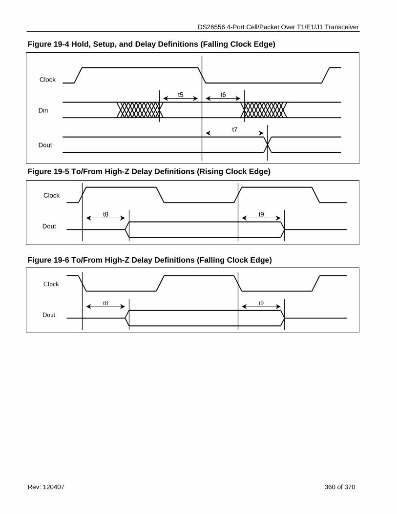
DS26556 4-Port Cell/Packet Over T1/E1/J1 Transceiver
Rev: 120407 360 of 370
Figure 19-4 Hold, Setup, and Delay Definitions (Falling Clock Edge)
Clock
Din
t5 t6
Dout
t7
Figure 19-5 To/From High-Z Delay Definitions (Rising Clock Edge)
Clock
Dout
t8 t9
Figure 19-6 To/From High-Z Delay Definitions (Falling Clock Edge)
Clock
Dout
t8 t9
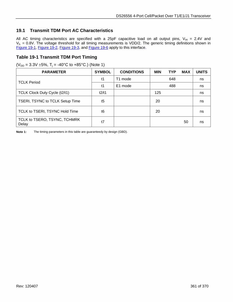
DS26556 4-Port Cell/Packet Over T1/E1/J1 Transceiver
Rev: 120407 361 of 370
19.1 Transmit TDM Port AC Characteristics
All AC timing characteristics are specified with a 25pF capacitive load on all output pins, VIH = 2.4V and VIL = 0.8V. The voltage threshold for all timing measurements is VDD/2. The generic timing definitions shown in Figure 19-1, Figure 19-2, Figure 19-3, and Figure 19-6 apply to this interface.
Table 19-1 Transmit TDM Port Timing (VDD = 3.3V ±5%, Tj = -40°C to +85°C.) (Note 1)
PARAMETER SYMBOL CONDITIONS MIN TYP MAX UNITS
t1 T1 mode 648 ns TCLK Period
t1 E1 mode 488 ns
TCLK Clock Duty Cycle (t2/t1) t2/t1 125 ns
TSERI, TSYNC to TCLK Setup Time t5 20 ns
TCLK to TSERI, TSYNC Hold Time t6 20 ns
TCLK to TSERO, TSYNC, TCHMRK Delay t7 50 ns
Note 1: The timing parameters in this table are guaranteedy by design (GBD).
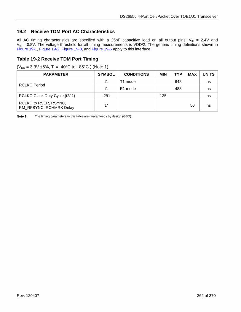
DS26556 4-Port Cell/Packet Over T1/E1/J1 Transceiver
Rev: 120407 362 of 370
19.2 Receive TDM Port AC Characteristics
All AC timing characteristics are specified with a 25pF capacitive load on all output pins, VIH = 2.4V and VIL = 0.8V. The voltage threshold for all timing measurements is VDD/2. The generic timing definitions shown in Figure 19-1, Figure 19-2, Figure 19-3, and Figure 19-6 apply to this interface.
Table 19-2 Receive TDM Port Timing (VDD = 3.3V ±5%, Tj = -40°C to +85°C.) (Note 1)
PARAMETER SYMBOL CONDITIONS MIN TYP MAX UNITS
t1 T1 mode 648 ns RCLKO Period
t1 E1 mode 488 ns
RCLKO Clock Duty Cycle (t2/t1) t2/t1 125 ns
RCLKO to RSER, RSYNC, RM_RFSYNC, RCHMRK Delay t7 50 ns
Note 1: The timing parameters in this table are guaranteedy by design (GBD).
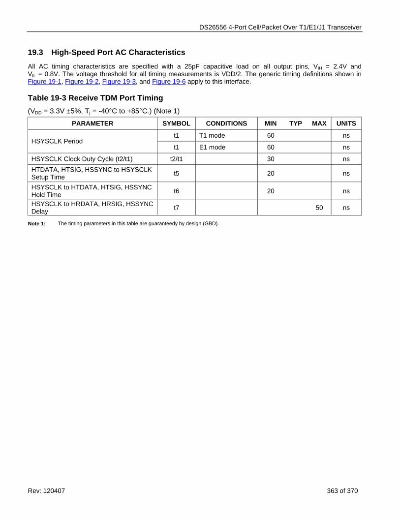
DS26556 4-Port Cell/Packet Over T1/E1/J1 Transceiver
Rev: 120407 363 of 370
19.3 High-Speed Port AC Characteristics
All AC timing characteristics are specified with a 25pF capacitive load on all output pins, VIH = 2.4V and VIL = 0.8V. The voltage threshold for all timing measurements is VDD/2. The generic timing definitions shown in Figure 19-1, Figure 19-2, Figure 19-3, and Figure 19-6 apply to this interface.
Table 19-3 Receive TDM Port Timing (VDD = 3.3V ±5%, Tj = -40°C to +85°C.) (Note 1)
PARAMETER SYMBOL CONDITIONS MIN TYP MAX UNITS
t1 T1 mode 60 ns HSYSCLK Period
t1 E1 mode 60 ns
HSYSCLK Clock Duty Cycle (t2/t1) t2/t1 30 ns HTDATA, HTSIG, HSSYNC to HSYSCLK Setup Time t5 20 ns
HSYSCLK to HTDATA, HTSIG, HSSYNC Hold Time t6 20 ns
HSYSCLK to HRDATA, HRSIG, HSSYNC Delay t7 50 ns
Note 1: The timing parameters in this table are guaranteedy by design (GBD).
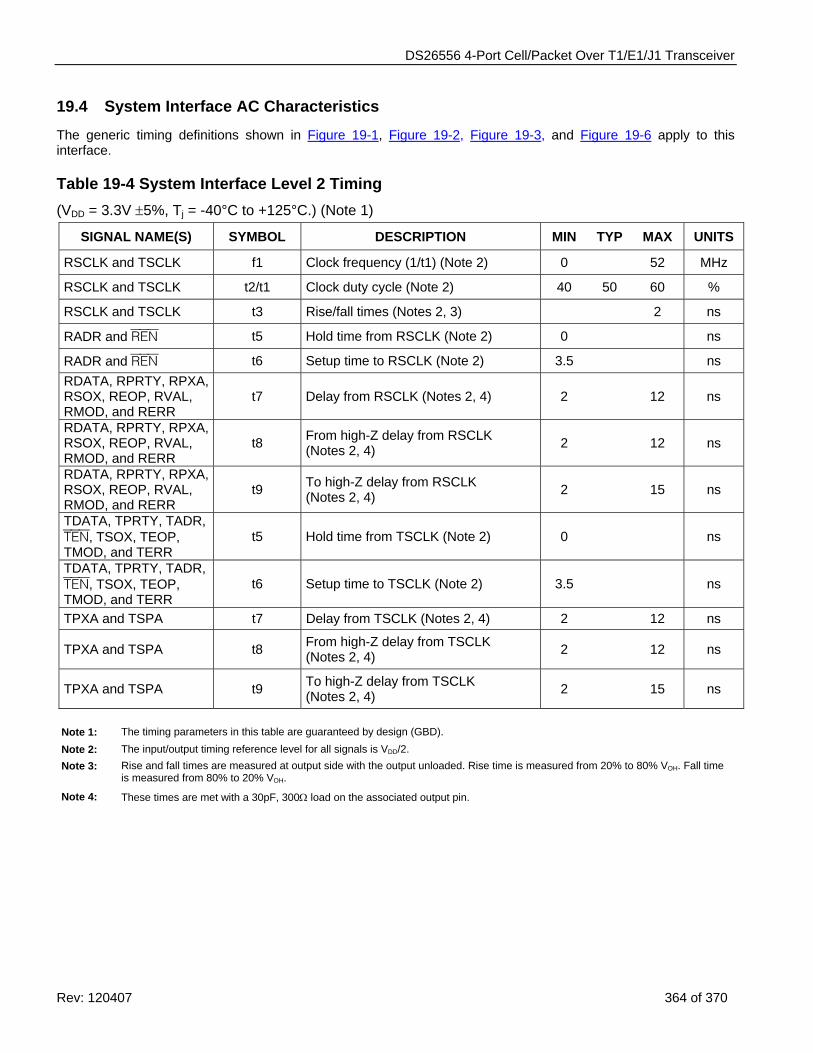
DS26556 4-Port Cell/Packet Over T1/E1/J1 Transceiver
Rev: 120407 364 of 370
19.4 System Interface AC Characteristics
The generic timing definitions shown in Figure 19-1, Figure 19-2, Figure 19-3, and Figure 19-6 apply to this interface.
Table 19-4 System Interface Level 2 Timing (VDD = 3.3V ±5%, Tj = -40°C to +125°C.) (Note 1)
SIGNAL NAME(S) SYMBOL DESCRIPTION MIN TYP MAX UNITS
RSCLK and TSCLK f1 Clock frequency (1/t1) (Note 2) 0 52 MHz
RSCLK and TSCLK t2/t1 Clock duty cycle (Note 2) 40 50 60 %
RSCLK and TSCLK t3 Rise/fall times (Notes 2, 3) 2 ns
RADR and REN t5 Hold time from RSCLK (Note 2) 0 ns
RADR and REN t6 Setup time to RSCLK (Note 2) 3.5 ns RDATA, RPRTY, RPXA, RSOX, REOP, RVAL, RMOD, and RERR
t7 Delay from RSCLK (Notes 2, 4) 2 12 ns
RDATA, RPRTY, RPXA, RSOX, REOP, RVAL, RMOD, and RERR
t8 From high-Z delay from RSCLK (Notes 2, 4) 2 12 ns
RDATA, RPRTY, RPXA, RSOX, REOP, RVAL, RMOD, and RERR
t9 To high-Z delay from RSCLK (Notes 2, 4) 2 15 ns
TDATA, TPRTY, TADR, TEN, TSOX, TEOP, TMOD, and TERR
t5 Hold time from TSCLK (Note 2) 0 ns
TDATA, TPRTY, TADR, TEN, TSOX, TEOP, TMOD, and TERR
t6 Setup time to TSCLK (Note 2) 3.5 ns
TPXA and TSPA t7 Delay from TSCLK (Notes 2, 4) 2 12 ns
TPXA and TSPA t8 From high-Z delay from TSCLK (Notes 2, 4) 2 12 ns
TPXA and TSPA t9 To high-Z delay from TSCLK (Notes 2, 4) 2 15 ns
Note 1: The timing parameters in this table are guaranteed by design (GBD). Note 2: The input/output timing reference level for all signals is VDD/2. Note 3: Rise and fall times are measured at output side with the output unloaded. Rise time is measured from 20% to 80% VOH. Fall time
is measured from 80% to 20% VOH.
Note 4: These times are met with a 30pF, 300Ω load on the associated output pin.
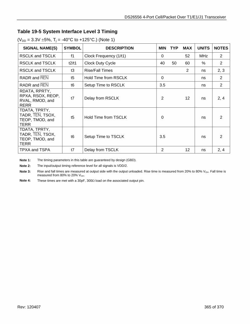
DS26556 4-Port Cell/Packet Over T1/E1/J1 Transceiver
Rev: 120407 365 of 370
Table 19-5 System Interface Level 3 Timing (VDD = 3.3V ±5%, Tj = -40°C to +125°C.) (Note 1)
SIGNAL NAME(S) SYMBOL DESCRIPTION MIN TYP MAX UNITS NOTES
RSCLK and TSCLK f1 Clock Frequency (1/t1) 0 52 MHz 2
RSCLK and TSCLK t2/t1 Clock Duty Cycle 40 50 60 % 2
RSCLK and TSCLK t3 Rise/Fall Times 2 ns 2, 3
RADR and REN t5 Hold Time from RSCLK 0 ns 2
RADR and REN t6 Setup Time to RSCLK 3.5 ns 2 RDATA, RPRTY, RPXA, RSOX, REOP, RVAL, RMOD, and RERR
t7 Delay from RSCLK 2 12 ns 2, 4
TDATA, TPRTY, TADR, TEN, TSOX, TEOP, TMOD, and TERR
t5 Hold Time from TSCLK 0 ns 2
TDATA, TPRTY, TADR, TEN, TSOX, TEOP, TMOD, and TERR
t6 Setup Time to TSCLK 3.5 ns 2
TPXA and TSPA t7 Delay from TSCLK 2 12 ns 2, 4
Note 1: The timing parameters in this table are guaranteed by design (GBD).
Note 2: The input/output timing reference level for all signals is VDD/2.
Note 3: Rise and fall times are measured at output side with the output unloaded. Rise time is measured from 20% to 80% VOH. Fall time is measured from 80% to 20% VOH.
Note 4: These times are met with a 30pF, 300Ω load on the associated output pin.
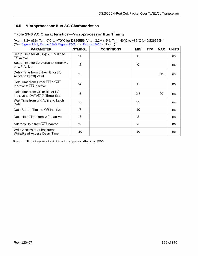
DS26556 4-Port Cell/Packet Over T1/E1/J1 Transceiver
Rev: 120407 366 of 370
19.5 Microprocessor Bus AC Characteristics
Table 19-6 AC Characteristics—Microprocessor Bus Timing (VDD = 3.3V ±5%, TA = 0°C to +70°C for DS26556; VDD = 3.3V ± 5%, TA = -40°C to +85°C for DS26556N.) (See Figure 19-7, Figure 19-8, Figure 19-9, and Figure 19-10) (Note 1)
PARAMETER SYMBOL CONDITIONS MIN TYP MAX UNITS Setup Time for ADDR[12:0] Valid to CS Active t1 0 ns
Setup Time for CS Active to Either RD or WR Active t2 0 ns
Delay Time from Either RD or DS Active to D[7:0] Valid t3 115 ns
Hold Time from Either RD or WR Inactive to CS Inactive t4 0 ns
Hold Time from CS or RD or DS Inactive to DATA[7:0] Three-State t5 2.5 20 ns
Wait Time from WR Active to Latch Data t6 35 ns
Data Set Up Time to WR Inactive t7 10 ns
Data Hold Time from WR Inactive t8 2 ns
Address Hold from WR Inactive t9 3 ns
Write Access to Subsequent Write/Read Access Delay Time t10 80 ns
Note 1: The timing parameters in this table are guaranteed by design (GBD).
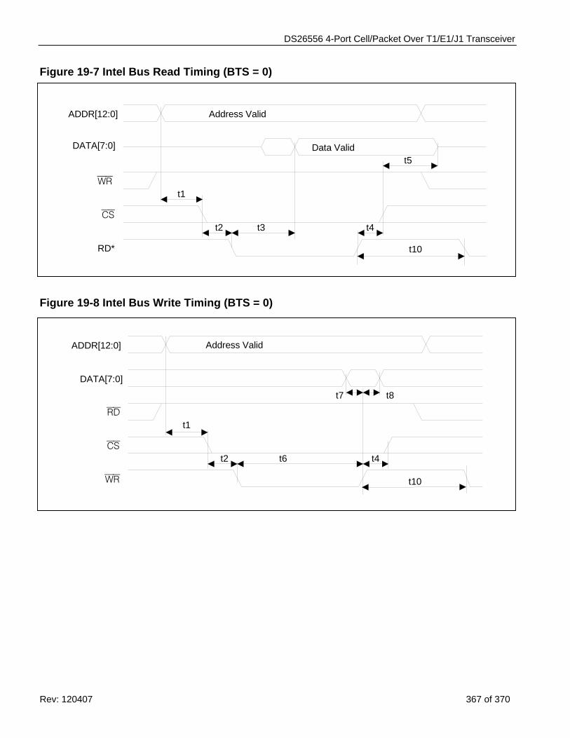
DS26556 4-Port Cell/Packet Over T1/E1/J1 Transceiver
Rev: 120407 367 of 370
Figure 19-7 Intel Bus Read Timing (BTS = 0)
Address Valid
Data Valid
ADDR[12:0]
DATA[7:0]
WR
CS
RD*
t1
t2 t3 t4
t5
t10
Figure 19-8 Intel Bus Write Timing (BTS = 0)
Address Valid
RD
CS
WR
t1
t2 t6 t4
t7 t8
ADDR[12:0]
DATA[7:0]
t10
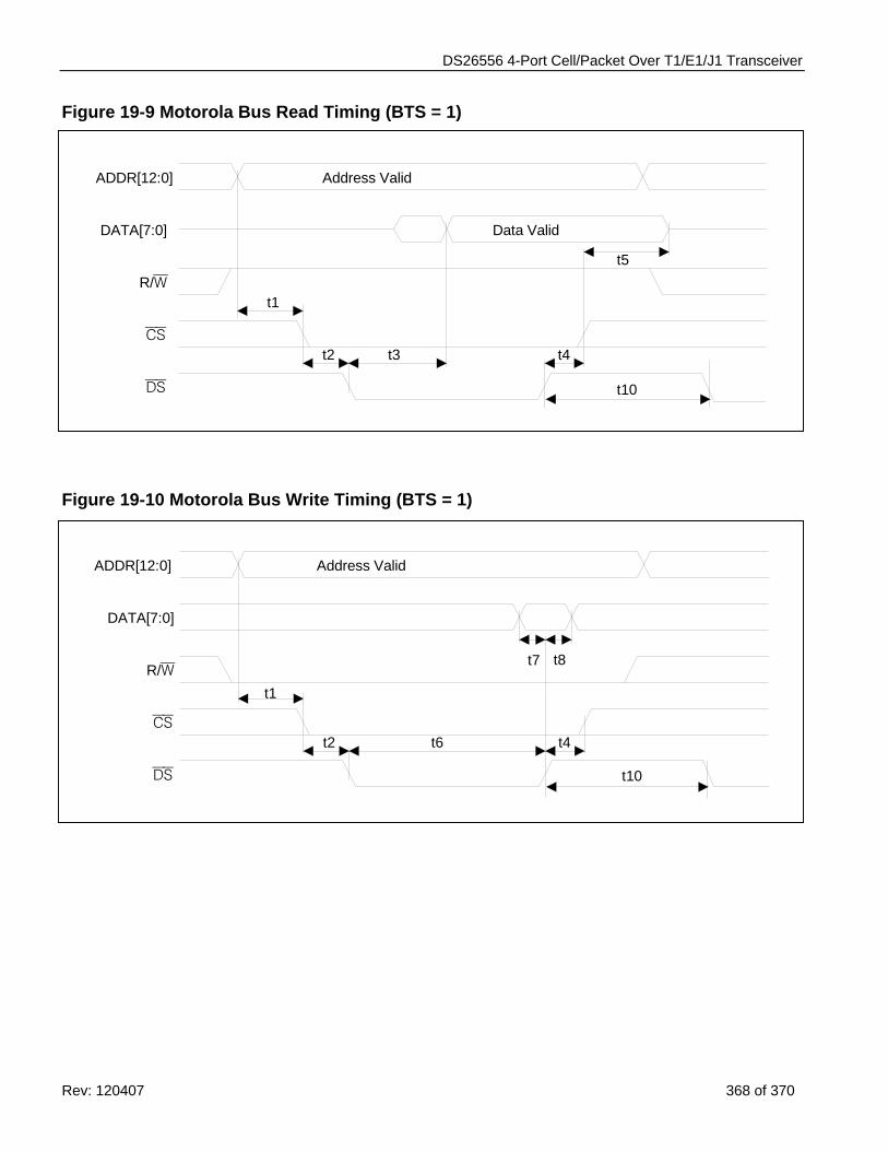
DS26556 4-Port Cell/Packet Over T1/E1/J1 Transceiver
Rev: 120407 368 of 370
Figure 19-9 Motorola Bus Read Timing (BTS = 1)
Address Valid
Data Valid
ADDR[12:0]
DATA[7:0]
R/W
CS
DS
t1
t2 t3 t4
t5
t10
Figure 19-10 Motorola Bus Write Timing (BTS = 1)
Address ValidADDR[12:0]
DATA[7:0]
R/W
CS
DS
t1
t2 t6 t4
t7 t8
t10
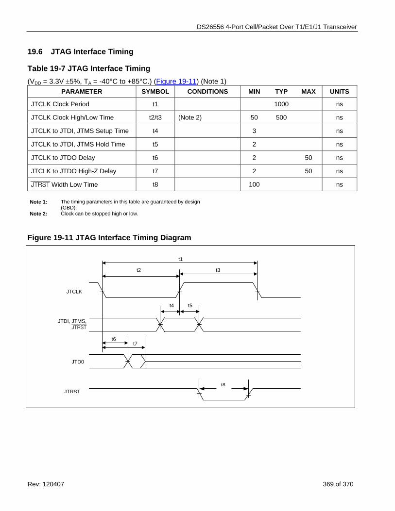
DS26556 4-Port Cell/Packet Over T1/E1/J1 Transceiver
Rev: 120407 369 of 370
19.6 JTAG Interface Timing
Table 19-7 JTAG Interface Timing (VDD = 3.3V ±5%, TA = -40°C to +85°C.) (Figure 19-11) (Note 1)
PARAMETER SYMBOL CONDITIONS MIN TYP MAX UNITS
JTCLK Clock Period t1 1000 ns
JTCLK Clock High/Low Time t2/t3 (Note 2) 50 500 ns
JTCLK to JTDI, JTMS Setup Time t4 3 ns
JTCLK to JTDI, JTMS Hold Time t5 2 ns
JTCLK to JTDO Delay t6 2 50 ns
JTCLK to JTDO High-Z Delay t7 2 50 ns
JTRST Width Low Time t8 100 ns
Note 1: The timing parameters in this table are guaranteed by design (GBD).
Note 2: Clock can be stopped high or low.
Figure 19-11 JTAG Interface Timing Diagram
JTCLK
t1
JTD0
t4 t5
t2 t3
t7
JTDI, JTMS, JTRST
t6
JTRSTt8
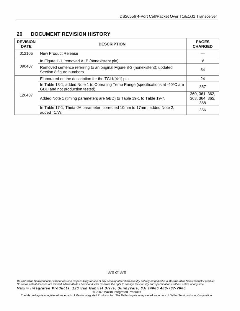
DS26556 4-Port Cell/Packet Over T1/E1/J1 Transceiver
370 of 370 Maxim/Dallas Semiconductor cannot assume responsibility for use of any circuitry other than circuitry entirely embodied in a Maxim/Dallas Semiconductor product. No circuit patent licenses are implied. Maxim/Dallas Semiconductor reserves the right to change the circuitry and specifications without notice at any time. Maxim Integrated Products , 120 San Gabr ie l Dr ive , Sunnyvale , CA 94086 408-737-7600
© 2007 Maxim Integrated Products The Maxim logo is a registered trademark of Maxim Integrated Products, Inc. The Dallas logo is a registered trademark of Dallas Semiconductor Corporation.
20 DOCUMENT REVISION HISTORY REVISION
DATE DESCRIPTION PAGES CHANGED
012105 New Product Release —
In Figure 1-1, removed ALE (nonexistent pin). 9 090407 Removed sentence referring to an original Figure 8-3 (nonexistent); updated
Section 8 figure numbers. 54
Elaborated on the description for the TCLK[4:1] pin. 24 In Table 18-1, added Note 1 to Operating Temp Range (specifications at -40°C are GBD and not production tested). 357
Added Note 1 (timing parameters are GBD) to Table 19-1 to Table 19-7. 360, 361, 362, 363, 364, 365,
368
120407
In Table 17-1, Theta-JA parameter: corrected 10mm to 17mm, added Note 2, added °C/W. 356