Embed Size (px)
Citation preview

Edition 1.8a
Jul. 2010 1
C-Band Internally Matched FET
ELM6472-4PS
Item Symbol Unit
Drain-Source Voltage VDS V
Gate-Source Voltage VGS V
Total Power Dissipation PT W
Storage Temperature TSTG deg.C
Channel Temperature TCH deg.C
Item Symbol Condition Unit
DC Input Voltage VDS V
Forward Gate Current IGF RG=100 ohm mA
Reverse Gate Current IGR RG=100 ohm mA
Channel Temperature TCH deg.C
Min. Typ. Max.
Drain Current IDSS VDS=5V, VGS=0V - 1700 2600 mA
Trans conductance gm VDS=5V, IDS=1100mA - 1700 - mS
Pinch-off Voltage VP VDS=5V, IDS=85mA -0.5 -1.5 -3.0 V
Output Power at 1dB G.C.P. P1dB 35.0 36.0 - dBm
Power Gain at 1dB G.C.P. G1dB 9.5 11.0 - dB
Drain Current Idsr - 1100 1300 mA
Power Added Efficiency hadd - 36 - %
Gain Flatness DG - - 1.2 dB
Rth Rth Channel to Case - 4.5 5.5 deg.C/W
DTch DTch 10V x Idsr x Rth - - 71.5 deg.C
155
ELECTRICAL CHARACTERISTICS (Case Temperature Tc=25 deg.C)
>-2.2
ABSOLUTE MAXIMUM RATING (Case Temperature Tc=25 deg.C)
Rating
15
-5
27.3
-40 to +125
175
RECOMMENDED OPERATING CONDITION (Case Temperature Tc=25 deg.C)
Limit
<10
<+16
Item Symbol ConditionLimit
Unit
-
dBc3rd Order Inter Modulation
DistortionIM3
f=7.2GHz
Df=10MHz, 2-tone Test
Pout=25.5dBm (S.C.L.)
-40 -43 -
Gate-Source
Breakdown VoltageVGSO IGS=85uA -5.0 -
VDS=10V
Ids(DC)=0.65IDSS(typ.)
f=6.4 to 7.2 GHz
V
FEATURES
High Output Power: P1dB=36.0dBm (Typ.)
High Gain: G1dB=11.0dB (Typ.)
High PAE: hadd=36% (Typ.)
Frequency Band: 6.4 to 7.2GHz
Internally matched
Plastic Package for SMT applications
DESCRIPTION
The ELM6472-4PS is a power GaAs FET that is internally matched for standard communication bands to provide optimum power and gain.

Edition 1.8a
Jul. 2010 2
C-Band Internally Matched FET
ELM6472-4PS
Note
• This device will not be delivered with test data but tested pass/fail 100% against DC and RF
specifications.
• NO liquid cleaning process is suitable for this device. (including de-ionized water or solvent)
ESD Class 3 A
MSL 2A
RoHS COMPLIANCE Yes
Model Type MOU Packing Style
ELM6472-4PS 15pcs 15pcs Tray
ELM6472-4PST 500pcs24mm width Tape
(500pcs/Reel)
*MOU stands for Minimum Order Unit size.
*MOQ stands for Minimum Order Quantity.
Ordering Information
MOQ
15pcs
CASE STYLE: I2C
4000 to 8000V
4 weeks after open the package
500pcs

Edition 1.8a
Jul. 2010 3
C-Band Internally Matched FET
ELM6472-4PS
-70
-65
-60
-55
-50
-45
-40
-35
-30
16 18 20 22 24 26 28 30
IM
D [
dB
c]
Output Power [dBm] S.C.L.
6.4 GHz 6.8 GHz 7.2 GHz
IM3
IM5
26
28
30
32
34
36
38
6.2 6.4 6.6 6.8 7 7.2 7.4
Ou
tpu
t P
ow
er
[dB
m]
Frequency [GHz]
17 dBm 19 dBm 21 dBm 23 dBm
25 dBm 27 dBm P1dB
0
10
20
30
40
50
60
26
28
30
32
34
36
38
15 17 19 21 23 25 27 29
Po
we
r A
dd
ed
Eff
icie
ncy [
%]
Ou
tpu
t P
ow
er
[dB
m]
Input Power [dBm]
6.4 GHz 6.8 GHz 7.2 GHz
0
5
10
15
20
25
30
0 50 100 150 200
To
tal P
ow
er
Dis
sip
ati
on
(W
)
Case Temperature (deg.C)
Power Derating Curve
Output Power vs. Frequency
VDS=10V, IDS(DC)=1100mA
IMD vs. Output Power
VDS=10V, IDS(DC)=1100mA
Input Power vs. Output Power,
Power Added Efficiency
VDS=10V, IDS(DC)=1100mA
RF Characteristics

Edition 1.8a
Jul. 2010 4
C-Band Internally Matched FET
ELM6472-4PS
0
10
20
30
40
50
60
26
28
30
32
34
36
38
15 17 19 21 23 25 27 29
Pp
we
r A
dd
ed
Eff
icie
ncy [
%]
Ou
tpu
t P
ow
er
[dB
m]
Input Power [dBm]
8V 9V 10V
0
10
20
30
40
50
60
26
28
30
32
34
36
38
15 17 19 21 23 25 27 29
Po
we
r A
dd
ed
Eff
icie
ncy [
%]
Ou
tpu
t P
ow
er
[dB
m]
Input Power [dBm]
8V 9V 10V
0
10
20
30
40
50
60
26
28
30
32
34
36
38
15 17 19 21 23 25 27 29
Po
we
r A
dd
ed
Eff
icie
ncy [
%]
Ou
tpu
t P
ow
er
[dB
m]
Input Power [dBm]
8V 9V 10V
Input Power vs. Output Power, Power Added
Efficiency by Drain Voltage
IDS(DC)=1100mA @6.8GHz
Input Power vs. Output Power, Power Added
Efficiency by Drain Voltage
IDS(DC)=1100mA @6.4GHz
Input Power vs. Output Power, Power Added
Efficiency by Drain Voltage
IDS(DC)=1100mA @7.2GHz

Edition 1.8a
Jul. 2010 5
C-Band Internally Matched FET
ELM6472-4PS
0
10
20
30
40
50
60
26
28
30
32
34
36
38
15 17 19 21 23 25 27 29
Po
we
r A
dd
ed
Eff
icie
ncy [
%]
Ou
tpu
t P
ow
er
[dB
m]
Input Power [dBm]
700mA 900mA 1100mA
0
10
20
30
40
50
60
26
28
30
32
34
36
38
15 17 19 21 23 25 27 29
Po
we
r A
dd
ed
Eff
icie
ncy [
%]
Ou
tpu
t P
ow
er
[dB
m]
Input Power [dBm]
700mA 900mA 1100mA
0
10
20
30
40
50
60
26
28
30
32
34
36
38
15 17 19 21 23 25 27 29
Po
we
r A
dd
ed
Eff
icie
ncy [
%]
Ou
tpu
t P
ow
er
[dB
m]
Input Power [dBm]
700mA 900mA 1100mA
Input Power vs. Output Power, Power Added
Efficiency by Quiescent Drain Current
VDS=10V @6.8GHz
Input Power vs. Output Power, Power Added
Efficiency by Quiescent Drain Current
VDS=10V @6.4GHz
Input Power vs. Output Power, Power Added
Efficiency by Quiescent Drain Current
VDS=10V @7.2GHz

Edition 1.8a
Jul. 2010 6
C-Band Internally Matched FET
ELM6472-4PS
Input Power vs. Output Power, Power Added
Efficiency by Temperature
VDS=10V @6.8GHz
Input Power vs. Output Power, Power Added
Efficiency by Temperature
VDS=10V @6.4GHz
Input Power vs. Output Power, Power Added
Efficiency by Temperature
VDS=10V @7.2GHz

Edition 1.8a
Jul. 2010 7
C-Band Internally Matched FET
ELM6472-4PS
-70
-65
-60
-55
-50
-45
-40
-35
-30
16 18 20 22 24 26 28 30
IM
D [
dB
c]
Output Power [dBm] S.C.L.
8V 9V 10V
IM3
IM5
-70
-65
-60
-55
-50
-45
-40
-35
-30
16 18 20 22 24 26 28 30
IM
D [
dB
c]
Output Power [dBm] S.C.L.
8V 9V 10V
IM3
IM5
-70
-65
-60
-55
-50
-45
-40
-35
-30
16 18 20 22 24 26 28 30
IM
D [
dB
c]
Output Power [dBm] S.C.L.
8V 9V 10V
IM3
IM5
IMD Performance vs. Output Power by Drain
Voltage
IDS(DC)=1100mA @6.8GHz
IMD Performance vs. Output Power by Drain
Voltage
IDS(DC)=1100mA @6.4GHz
IMD Performance vs. Output Power by
Drain Voltage
IDS(DC)=1100mA @7.2GHz

Edition 1.8a
Jul. 2010 8
C-Band Internally Matched FET
ELM6472-4PS
-70
-65
-60
-55
-50
-45
-40
-35
-30
16 18 20 22 24 26 28 30
IM
D [
dB
c]
Output Power [dBm] S.C.L.
700mA 900mA 1100mA
IM3
IM5
-70
-65
-60
-55
-50
-45
-40
-35
-30
16 18 20 22 24 26 28 30
IM
D [
dB
c]
Output Power [dBm] S.C.L.
700mA 900mA 1100mA
IM3
IM5
-70
-65
-60
-55
-50
-45
-40
-35
-30
16 18 20 22 24 26 28 30
IM
D [
dB
c]
Output Power [dBm] S.C.L.
700mA 900mA 1100mA
IM3
IM5
IMD Performance vs. Output Power by
Quiescent Drain Current
VDS=10V @6.8GHz
IMD Performance vs. Output Power by
Quiescent Drain Current
VDS=10V @6.4GHz
IMD Performance vs. Output Power by
Quiescent Drain Current
VDS=10V @7.2GHz

Edition 1.8a
Jul. 2010 9
C-Band Internally Matched FET
ELM6472-4PS
IMD Performance vs. Output Power by
Temperature
VDS=10V @6.8GHz
IMD Performance vs. Output Power by
Temperature
VDS=10V @6.4GHz
IMD Performance vs. Output Power by
Temperature
VDS=10V @7.2GHz

Edition 1.8a
Jul. 2010 10
C-Band Internally Matched FET
ELM6472-4PS
Frequency
(MHz) MAG ANG MAG ANG MAG ANG MAG ANG
6200 0.696 -168.6 3.710 -14.2 0.054 79.8 0.553 -140.7
6300 0.683 175.8 3.777 -29.7 0.051 64.6 0.558 -157.2
6400 0.664 160.9 3.840 -44.6 0.047 49.5 0.562 -172.8
6500 0.644 146.2 3.877 -59.2 0.042 34.5 0.564 173.3
6600 0.620 131.4 3.924 -73.6 0.037 19.1 0.564 159.7
6700 0.587 116.5 3.981 -87.9 0.032 4.7 0.562 147.6
6800 0.554 101.4 4.083 -102.4 0.028 -12.7 0.556 136.5
6900 0.516 83.9 4.218 -117.2 0.024 -33.6 0.540 125.0
7000 0.468 63.1 4.412 -133.4 0.019 -59.3 0.513 113.6
7100 0.419 37.5 4.590 -151.0 0.015 -95.1 0.467 101.4
7200 0.381 4.8 4.735 -170.2 0.014 -140.1 0.399 88.4
7300 0.380 -33.9 4.727 168.6 0.015 173.6 0.303 74.4
7400 0.426 -71.1 4.535 146.8 0.019 133.6 0.183 60.9
S11 S21 S12 S22
S21
S12
±180 0
-
+90
Sca
le fo
r |S
12|
2
Scale for |S21|
S-Parameter
Gate Drain
S-Parameter
Reference Plane

Edition 1.8a
Jul. 2010 11
C-Band Internally Matched FET
ELM6472-4PS
Co Planarity
Pin Assignments
1 : NC
2 : Gate
3 : NC
4 : NC
5 : Drain
6 : NC
7 : Source
1
2
34
5
6
7
Package Outline

Edition 1.8a
Jul. 2010 12
C-Band Internally Matched FET
ELM6472-4PS
PCB Pads and Solder-Resist Pattern

Edition 1.8a
Jul. 2010 13
C-Band Internally Matched FET
ELM6472-4PS
Marking and Tape/Reel Configuration

Edition 1.8a
Jul. 2010 14
C-Band Internally Matched FET
ELM6472-4PS
Mounting Instructions for Package for Lead-free solder
Mounting Condition For soldering, Lead-free solder (Sn-3.0Ag-0.5Cu)*1 or equivalent shall be used.
1. The example solder is a tin-rich alloy with 3.0% silver and 0.5% copper, often called Sn 96 for its
approximate Tin content.
2. A rosin type flux with chlorine content of 0.2% or less shall be used. The rosin flux with low halogen
content is recommended. When soldering, use the following time/ temperature profile with any of the
methods listed for acceptable solder joints.
3. Make sure the devices have been properly prepared with flux prior soldering.
* Reflow soldering method (Infrared reflow / Heat circulation reflow / Hot plate reflow); Limit solder to 3 reflow cycles because resin is used in the modules manufacturing process.
Excessive reflow will effect the resin resulting in a potential failure or latent defect.
The recommended reflow temperature profile is shown below. The temperature of the reflow profile
must be measured at the device lead.
Reflow temperature profile and condition:
(1). Temperature rise: 3 deg.C/seconds.
(2). Preheating: 150 to 200 deg.C, 60 to 180seconds.
(3). Main heating: 220 deg.C, 60 seconds max.
(4). Main heating: 260 deg.C max., more than 250 deg.C, 20 to 40 seconds max.
* Measurement point: Device Heat-sink (Source Pin).
1. The above-recommended conditions were confirmed using the manufacturer’s equipment and materials.
However, when soldering these products, the soldering condition should be verified by customer using
their own particular equipment and materials.
Cleaning
Avoid washing of the device after soldering by reflow method due to the risk of liquid absorption by the
resin used in this part.
Tem
pera
ture
(deg.C
)
260 250 220
200
140
RT (1)
(2)
(3)
(4)
Time
Edition 1.8a
Jul. 2010 15
C-Band Internally Matched FET
ELM6472-4PS
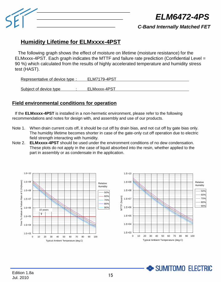
Humidity Lifetime for ELMxxxx-4PST
The following graph shows the effect of moisture on lifetime (moisture resistance) for the
ELMxxxx-4PST. Each graph indicates the MTTF and failure rate prediction (Confidential Level =
90 %) which calculated from the results of highly accelerated temperature and humidity stress
test (HAST).
Representative of device type : ELM7179-4PST
Subject of device type : ELMxxxx-4PST
1.E+03
1.E+04
1.E+05
1.E+06
1.E+07
1.E+08
1.E+09
1.E+10
0 10 20 30 40 50 60 70 80 90 100
Typical Ambient Temperature (deg.C)
Tim
e T
o F
ailu
re a
t F
ailu
re R
ate
of
0.1
%(h
ours
)
50%
60%
70%
80%
90%
Relative
Humidity
10 years
1.E+03
1.E+04
1.E+05
1.E+06
1.E+07
1.E+08
1.E+09
1.E+10
0 10 20 30 40 50 60 70 80 90 100
Typical Ambient Temperature (deg.C)
MT
TF
(h
ou
rs)
50%
60%
70%
80%
90%
Relative
Humidity
Field environmental conditions for operation
If the ELMxxxx-4PST is installed in a non-hermetic environment, please refer to the following
recommendations and notes for design with, and assembly and use of our products.
Note 1. When drain current cuts off, it should be cut off by drain bias, and not cut off by gate bias only.
The humidity lifetime becomes shorter in case of the gate-only cut off operation due to electric
field strength interacting with humidity.
Note 2. ELMxxxx-4PST should be used under the environment conditions of no dew condensation.
These plots do not apply in the case of liquid absorbed into the resin, whether applied to the
part in assembly or as condensate in the application.

Edition 1.8a
Jul. 2010 16
C-Band Internally Matched FET
ELM6472-4PS
For further information please contact:
http://global-sei.com/Electro-optic/about/office.html
CAUTION
This product contains gallium arsenide (GaAs) which can be hazardous to the human body and the environment. For
safety, observe the following procedures:
・Do not put these products into the mouth.
・Do not alter the form of this product into a gas, powder, or liquid through burning, crushing, or chemical processing as
these by-products are dangerous to the human body if inhaled, ingested, or swallowed.
・Observe government laws and company regulations when discarding this product. This product must be discarded in
accordance with methods specified by applicable hazardous waste procedures.