Embed Size (px)
Citation preview
1 of 31 013100
FEATURES Unique 1-WireTM interface requires only one
port pin for communication Provides unique 64-bit serial number to
battery packs Eliminates thermistors by sensing battery
temperature on-chip On-board A/D converter allows monitoring of
battery voltage for end-of-charge and end-of-discharge determination
On-board integrated current accumulatorfacilitates gas gauging
Real-time clock in binary format 40-byte nonvolatile user memory available for
storage of user data such as gas gauge andmanufacturing information
Operating range -40°C to +85°C Applications include portable computers,
portable/cellular phones, consumerelectronics, and handheld instrumentation
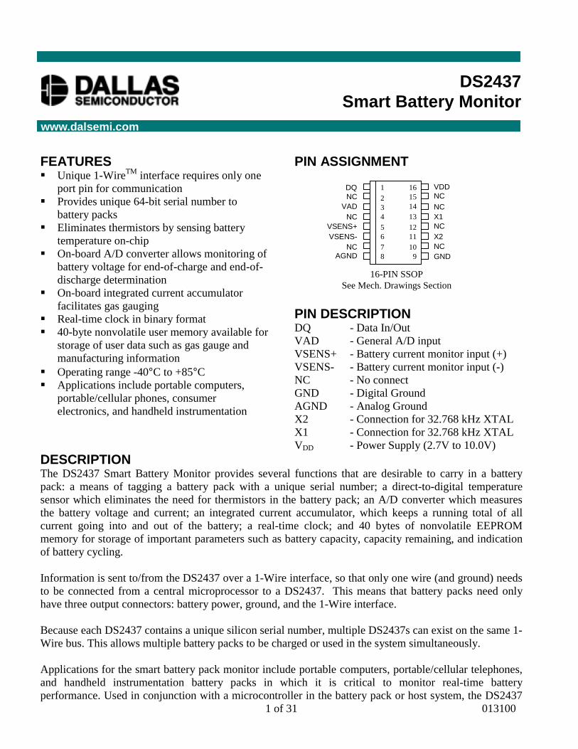
PIN ASSIGNMENT
PIN DESCRIPTIONDQ - Data In/OutVAD - General A/D inputVSENS+ - Battery current monitor input (+)VSENS- - Battery current monitor input (-)NC - No connectGND - Digital GroundAGND - Analog GroundX2 - Connection for 32.768 kHz XTALX1 - Connection for 32.768 kHz XTALVDD - Power Supply (2.7V to 10.0V)
DESCRIPTIONThe DS2437 Smart Battery Monitor provides several functions that are desirable to carry in a batterypack: a means of tagging a battery pack with a unique serial number; a direct-to-digital temperaturesensor which eliminates the need for thermistors in the battery pack; an A/D converter which measuresthe battery voltage and current; an integrated current accumulator, which keeps a running total of allcurrent going into and out of the battery; a real-time clock; and 40 bytes of nonvolatile EEPROMmemory for storage of important parameters such as battery capacity, capacity remaining, and indicationof battery cycling.
Information is sent to/from the DS2437 over a 1-Wire interface, so that only one wire (and ground) needsto be connected from a central microprocessor to a DS2437. This means that battery packs need onlyhave three output connectors: battery power, ground, and the 1-Wire interface.
Because each DS2437 contains a unique silicon serial number, multiple DS2437s can exist on the same 1-Wire bus. This allows multiple battery packs to be charged or used in the system simultaneously.
Applications for the smart battery pack monitor include portable computers, portable/cellular telephones,and handheld instrumentation battery packs in which it is critical to monitor real-time batteryperformance. Used in conjunction with a microcontroller in the battery pack or host system, the DS2437
DS2437Smart Battery Monitor
www.dalsemi.com
16-PIN SSOPSee Mech. Drawings Section
15VAD
VSENS+
NCAGND
VDD
X1NCX2NCGND
12345678
16
1413121110
9
NC
NC
VSENS-
DQNCNC
DS2437
2 of 31
provides a complete smart battery pack solution that is fully chemistry-independent. The customizationfor a particular battery chemistry and capacity is realized in the code programmed into themicrocontroller and DS2437 EEPROM, and only a software revision is necessary should a designer wishto change battery pack chemistry.
DETAILED PIN DESCRIPTIONPIN SYMBOL DESCRIPTION
1 DQ Data Input/Out: for 1-Wire operation: open drain3 VAD ADC Input: input for general purpose A/D5 VSENS+ Battery Input: connection for battery current to be monitored (see text)6 VSENS- Battery Input: connection for battery current to be monitored (see text)8 AGND Analog Ground: must be at the same potential as GND9 GND Digital Ground: must be at the same potential as AGND11 X2 Crystal Input: connection for 32.768 kHz for RTC operation13 X1 Crystal Input: connection for 32.768 kHz for RTC operation16 VDD VDD Pin: input supply voltage
2, 4, 7, 10,12, 14, 15
NC No Connect
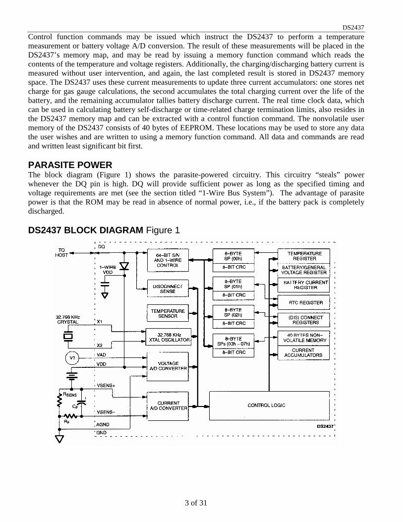
OVERVIEWThe block diagram of Figure 1 shows the seven major components of the DS2437:1. 64-bit lasered ROM2. temperature sensor3. battery voltage A/D4. battery current A/D5. current accumulators6. real-time clock7. 40-byte nonvolatile user memoryEach DS2437 contains a unique 64-bit lasered ROM serial number so that several battery packs can becharged/monitored by the same host system. Furthermore, other Dallas products featuring the same 1-Wire bus architecture with a 64-bit ROM can reside on the same bus; refer to the Dallas "AutomaticIdentification Data Book" for the specifications of these products.
Communication to the DS2437 is via a 1-Wire port. With the 1-Wire port, the memory and controlfunctions will not be available until the ROM function protocol has been established. The master mustfirst provide one of four ROM function commands: 1) Read ROM, 2) Match ROM, 3) Search ROM, or 4)Skip ROM. These commands operate on the 64-bit lasered ROM portion of each device and can singulatea specific device if many are present on the 1-Wire line as well as indicate to the bus master how manyand what types of devices are present. After a ROM function sequence has been successfully executed,the memory and control functions are accessible and the master may then provide any one of the sixmemory and control function commands.
DS2437
3 of 31
Control function commands may be issued which instruct the DS2437 to perform a temperaturemeasurement or battery voltage A/D conversion. The result of these measurements will be placed in theDS2437’s memory map, and may be read by issuing a memory function command which reads thecontents of the temperature and voltage registers. Additionally, the charging/discharging battery current ismeasured without user intervention, and again, the last completed result is stored in DS2437 memoryspace. The DS2437 uses these current measurements to update three current accumulators: one stores netcharge for gas gauge calculations, the second accumulates the total charging current over the life of thebattery, and the remaining accumulator tallies battery discharge current. The real time clock data, whichcan be used in calculating battery self-discharge or time-related charge termination limits, also resides inthe DS2437 memory map and can be extracted with a control function command. The nonvolatile usermemory of the DS2437 consists of 40 bytes of EEPROM. These locations may be used to store any datathe user wishes and are written to using a memory function command. All data and commands are readand written least significant bit first.
PARASITE POWERThe block diagram (Figure 1) shows the parasite-powered circuitry. This circuitry “steals” powerwhenever the DQ pin is high. DQ will provide sufficient power as long as the specified timing andvoltage requirements are met (see the section titled “1-Wire Bus System”). The advantage of parasitepower is that the ROM may be read in absence of normal power, i.e., if the battery pack is completelydischarged.
DS2437 BLOCK DIAGRAM Figure 1
DS2437
4 of 31
OPERATION – MEASURING TEMPERATUREThe DS2437 measures temperatures through the use of an onboard proprietary temperature measurementtechnique.
The temperature reading is provided in a 13-bit, two’s complement reading, which provides 0.03125°C ofresolution. Table 1 describes the exact relationship of output data to measured temperature. The data istransmitted serially over the 1-Wire interface. The DS2437 can measure temperature over the range of-55°C to +125°C in 0.03125°C increments. For Fahrenheit usage, a lookup table or conversion factormust be used.
Note that temperature is represented in the DS2437 in terms of a 0.03125°C LSb, yielding the following13-bit format. The 3 least significant bits of the temperature register will always be 0. The remaining 13bits contain the two’s complement representation of the temperature in °C, with the MSb holding the sign(S) bit. See “Memory Map” section for the TEMPERATURE REGISTER address location.
Temperature/Data Relationships Table 1
TEMPERATURE DIGITAL OUTPUT (Binary) DIGITAL OUTPUT (Hex)+125°C 01111101 00000000 7D00h
+25.0625°C 00011001 00010000 1910h
+1/2°C 00000000 10000000 0080h
0°C 00000000 00000000 0000h
-1/2°C 11111111 10000000 FF80h
-25.0625°C 11100110 11110000 E6F0h
-55°C 11001001 00000000 C900h
OPERATION – MEASURING BATTERY VOLTAGEThe on-board analog-to-digital converter (ADC) has 10 bits of resolution and will perform a conversionwhen the DS2437 receives a command protocol (Convert V) instructing it to do so. The result of thismeasurement is placed in the 2-byte VOLTAGE REGISTER. The range for the DS2437 ADC is 0V to10V; this range is suitable for NiCd or NiMH battery packs up to six cells and for lithium ion batterypacks of two cells. The full-scale range of the ADC is scaled to 10.23V, resulting in a resolution of 10mV.
While the ADC has a range that extends to 0V, it is important to note that the battery voltage can also bethe supply voltage to the DS2437. As such, the accuracy of the ADC begins to degrade below batteryvoltages of 2.7V, and the ability to make conversions is limited by the operating voltage range of theDS2437.
Voltage is expressed in this register in scaled binary format, as outlined in Table 2. Note that while codesexist for values below 2.7V, accuracy of the ADC and the limitation on the DS2437’s supply voltage
DS2437
5 of 31
make it unlikely that these values would be used in actual practice. See “Memory Map” section for theVOLTAGE REGISTER address location.
Voltage/Data Relationships Table 2
BATTERYVOLTAGE DIGITAL OUTPUT (Binary) DIGITAL OUTPUT (Hex)
0.01V 0000 0000 0000 0001 0001h2.7 0000 0001 0000 1110 010Eh
3.6V 0000 0001 0110 1000 0168h5V 0000 0001 1111 0100 01F4h
7.2V 0000 0010 1101 0000 02D0h9.99V 0000 0011 1110 0111 03E7h10V 0000 0011 1110 1000 03E8h
For applications requiring a general purpose voltage A/D converter, the DS2437 can be configured so thatthe result of a Convert V command will place the scaled binary representation of the voltage on the VADinput (as opposed to the VDD input) into the VOLTAGE REGISTER in the same format described inTable 2. Depending upon the state of the configuration register, either (but not both) the VDD or VADvoltage will be stored in the VOLTAGE REGISTER upon receipt of the Convert V command. Refer tothe description of the Configuration Register in the Memory Map section for details. If the VAD input isused as the voltage input, the A/D will be accurate for 0V < VAD < 2VDD over the range 2.7V < VDD <5.0V. Recall that the battery voltage A/D (VDD input) loses accuracy as VDD falls below 2.7V. Thisfeature gives the user the ability to have a voltage A/D that meets spec accuracy for inputs over the entirerange of 0V < VAD < 10V for VDD = 5.0V.
OPERATION – MEASURING BATTERY CURRENTThe DS2437 features a sigma-delta A/D converter that effectively measures the current flow into and outof the battery pack. It does so in the background at a rate of 32 measurements/sec; thus, no command isrequired to initiate current flow measurements. However, the DS2437 will only perform current A/Dmeasurements if the IAD bit is set to 1 in the CONFIGURATION REGISTER. The DS2437 measurescurrent flow in and out of the battery through the VSENS pins; the voltage from the VSENS+ pin to theVSENS- pin is considered to be the voltage across the current sense resistor, RSENS. While the VSENS+terminal may be tied directly to the cell side of the RSENS resistor, we recommend using an RC low passfilter between the other side of RSENS and VSENS-. Using a 47 kΩ=(max) resistor (RF) and a 0.1 µFcapacitor (CF), the filter cutoff is approximately 32 Hz. The current A/D measures at a rate of 32 timesper second, or once every 31.25 ms. This filter will capture the effect of many current spikes and will thusallow the current accumulators to accurately reflect the total charge which has gone into or out of thebattery.
The current is measured by the ADC with a signed 10-bit (0.004883C) resolution, and the last completedmeasurement is placed in the CURRENT REGISTER in a sign-extended 2’s-complement format. This
DS2437
6 of 31
register is scaled such that a count of 20510 corresponds to a current level of 1C. Thus, the range ofcurrent flow that can be measured is from -2.5C (discharging) to +2.5C (charging). The sign (S) of thecurrent measurement, indicating charge or discharge, resides in the seven most significant bits of theCURRENT REGISTER, as shown in Table 3. See “Memory Map” section for the CURRENTREGISTER address location.
Current/Data Relationships Table 3
BATTERYCURRENT DIGITAL OUTPUT (Binary) DIGITAL OUTPUT (Hex)
+2.495C 0000 0001 1111 1111 01FFh+2.002C 0000 0001 1001 1010 019Ah+1.25C 0000 0001 0000 0000 0100h+1.001C 0000 0000 1100 1101 00CDh
0C 0000 0000 0000 0000 0000h-1.001C 1111 1111 0011 0011 FF33h-1.25C 1111 1111 0000 0000 FF00h-2.002C 1111 1110 0110 0110 FE66h-2.500C 1111 1110 0000 0000 FE00h
For the DS2437 to output current data scaled as in Table 3, the user is responsible for selecting an RSENSthat will provide a 100 mV drop across it at a 2C rate. However, this value could be changed tocorrespond to a different rate as long as this is comprehended by the user’s software in interpreting theresults from the DS2437.
OPERATION – CURRENT ACCUMULATORSThe DS2437 keeps track of the remaining capacity of a battery through the Integrated CurrentAccumulator (ICA). The ICA maintains a net accumulated total of current flowing into and out of thebattery; therefore, the reading in this register is an indication of the remaining capacity in a battery andmay be used in performing gas gauge functions. In addition, the DS2437 has a register that accumulatesbattery charging (positive) current (CCA) and one that accumulates discharging (negative) current(DCA). This gives the smart battery system information needed to determine the end of life of arechargeable battery, based on total charge/discharge current over its lifetime.
The current measurement described above yields a result of the instantaneous current measured at the31.25 ms measurement times. This value is then used to increment or decrement the ICA register,increment the CCA (if current is positive), or increment the DCA (if current is negative).
The ICA is a scaled 8-bit (0.01C resolution) volatile binary counter which represents the amount ofcapacity remaining in the battery in terms of the full capacity (1C), normalized to a count of 10010. Thus,an ICA count of 10010 represents 1C of charge or 100% of capacity or fully charged, while a count of 0
DS2437
7 of 31
represents 0% of capacity or fully discharged. The ICA will count up to 25510, but will not roll over ifincremented above 2.55C, which should not occur during charging. However, since charging typicallyprovides the battery with more than its rated capacity, the ICA should be reset to a count of 10010 whencharging is complete to indicate that the battery is at 100% of capacity and to ensure that later gas gaugemeasurements are accurate.
The ICA is only incremented/decremented if the IAD bit is set to 1 in the CONFIGURATIONREGISTER. Refer to the “Memory Map” section for details of device configuration. Table 4 belowillustrates the contents of the ICA. See Memory Map section for the address location of the ICA.
ICA/Data Relationships Table 4
BATTERYCAPACITY DIGITAL OUTPUT (Binary) DIGITAL OUTPUT (Hex)
2.55C 1111 1111 FFh1.0C 0110 0100 64h0.5C 0011 0010 32h0.1C 0000 1010 0Ah0C 0000 0000 00h
The Charging Current Accumulator (CCA) is a 2-byte (0.32C resolution) nonvolatile read/write counterwhich represents the total charging current the battery has encountered in its lifetime. It is only updatedwhen current through RSENS is positive; i.e., the battery is being charged. Because this is a nonvolatileregister, the information will accumulate over the lifetime of the battery pack and will not be lost whenthe battery becomes discharged.
Similarly, the Discharge Current Accumulator (DCA) is a 2-byte nonvolatile counter which represents thetotal discharging current the battery has encountered over its lifetime. It features the same resolution asthe CCA and it also is shadowed to EEPROM in the background at the rate of once per 0.32C ofdischarge current if the DS2437 is properly configured, thus allowing three EEPROM updates for eachcomplete discharge cycle of the battery pack. Table 5 illustrates the contents of the CCA/DCA registers.
In reference to the CCA/DCA, the DS2437 can be configured to function in any of three modes. Refer tothe Memory Map section for details of device configuration and for the address location of theCCA/DCA.1. The CCA/DCA is disabled. Charging/discharging current will not be accumulated, thus allowing free
use of EEPROM page 07h otherwise reserved for the CCA/DCA.2. The CCA/DCA will accumulate charging/discharging current, but the information will NOT be
shadowed to EEPROM. The information could be lost or corrupted upon discharge of the battery(depending upon the voltage to which discharged battery decays). The memory location is reservedfor the CCA/DCA, and the entire page SHOULD NOT be written to.
DS2437
8 of 31
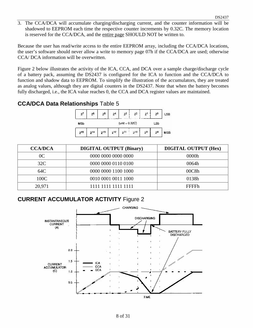
3. The CCA/DCA will accumulate charging/discharging current, and the counter information will beshadowed to EEPROM each time the respective counter increments by 0.32C. The memory locationis reserved for the CCA/DCA, and the entire page SHOULD NOT be written to.
Because the user has read/write access to the entire EEPROM array, including the CCA/DCA locations,the user’s software should never allow a write to memory page 07h if the CCA/DCA are used; otherwiseCCA/ DCA information will be overwritten.
Figure 2 below illustrates the activity of the ICA, CCA, and DCA over a sample charge/discharge cycleof a battery pack, assuming the DS2437 is configured for the ICA to function and the CCA/DCA tofunction and shadow data to EEPROM. To simplify the illustration of the accumulators, they are treatedas analog values, although they are digital counters in the DS2437. Note that when the battery becomesfully discharged, i.e., the ICA value reaches 0, the CCA and DCA register values are maintained.
CCA/DCA Data Relationships Table 5
CCA/DCA DIGITAL OUTPUT (Binary) DIGITAL OUTPUT (Hex)0C 0000 0000 0000 0000 0000h32C 0000 0000 0110 0100 0064h64C 0000 0000 1100 1000 00C8h100C 0010 0001 0011 1000 0138h
20,971 1111 1111 1111 1111 FFFFh
CURRENT ACCUMULATOR ACTIVITY Figure 2
DS2437
9 of 31
OPERATION – REAL TIME CLOCKThe 32.768 kHz crystal oscillator is used as the time base for the timekeeping functions. The timekeepingfunctions are double-buffered, allowing the master to read time without the data changing while it isbeing read. To accomplish this, a snapshot of the counter data is transferred to holding registers which theuser accesses. This occurs after the eighth bit of the Recall Memory command.
The real-time clock is a 4-byte binary counter with a 1-second resolution. The four bytes are a count ofseconds. The real-time clock can accumulate 136 years of seconds before rolling over. Time/date isrepresented by the number of seconds since a reference point, which is determined by the user. Forexample, 12:00 A.M., January 1, 1970 could be used as a reference point.
Two other time-related functions are available. The first is the DISCONNECT TIMESTAMP, which iswritten to by the DS2437 whenever it senses that the DQ line has been low for more than 1 second. Thiscondition would signal that the battery pack has been removed from the system; the time when thatoccurs is written into the DISCONNECT TIMESTAMP register, so that upon replacement into thesystem, the system can determine how long the device has been in storage, to facilitate self-dischargecorrections to the remaining battery capacity. After the disconnect has been detected, the DS2437 revertsto a sleep mode, during which nothing is active except the real time clock.
The other timestamp is the END OF CHARGE timestamp, which is written to by the DS2437 whenever itsenses that charging is finished (when current changes direction). This timestamp allows the user tocalculate the amount of time the battery has been in a discharge or storage state, again to facilitate self-discharge calculations.
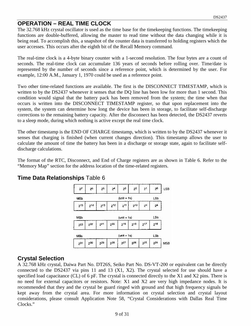
The format of the RTC, Disconnect, and End of Charge registers are as shown in Table 6. Refer to the“Memory Map” section for the address location of the time-related registers.
Time Data Relationships Table 6
Crystal SelectionA 32.768 kHz crystal, Daiwa Part No. DT26S, Seiko Part No. DS-VT-200 or equivalent can be directlyconnected to the DS2437 via pins 11 and 13 (X1, X2). The crystal selected for use should have aspecified load capacitance (CL) of 6 pF. The crystal is connected directly to the X1 and X2 pins. There isno need for external capacitors or resistors. Note: X1 and X2 are very high impedance nodes. It isrecommended that they and the crystal be guard ringed with ground and that high frequency signals bekept away from the crystal area. For more information on crystal selection and crystal layoutconsiderations, please consult Application Note 58, “Crystal Considerations with Dallas Real TimeClocks.”
DS2437
10 of 31
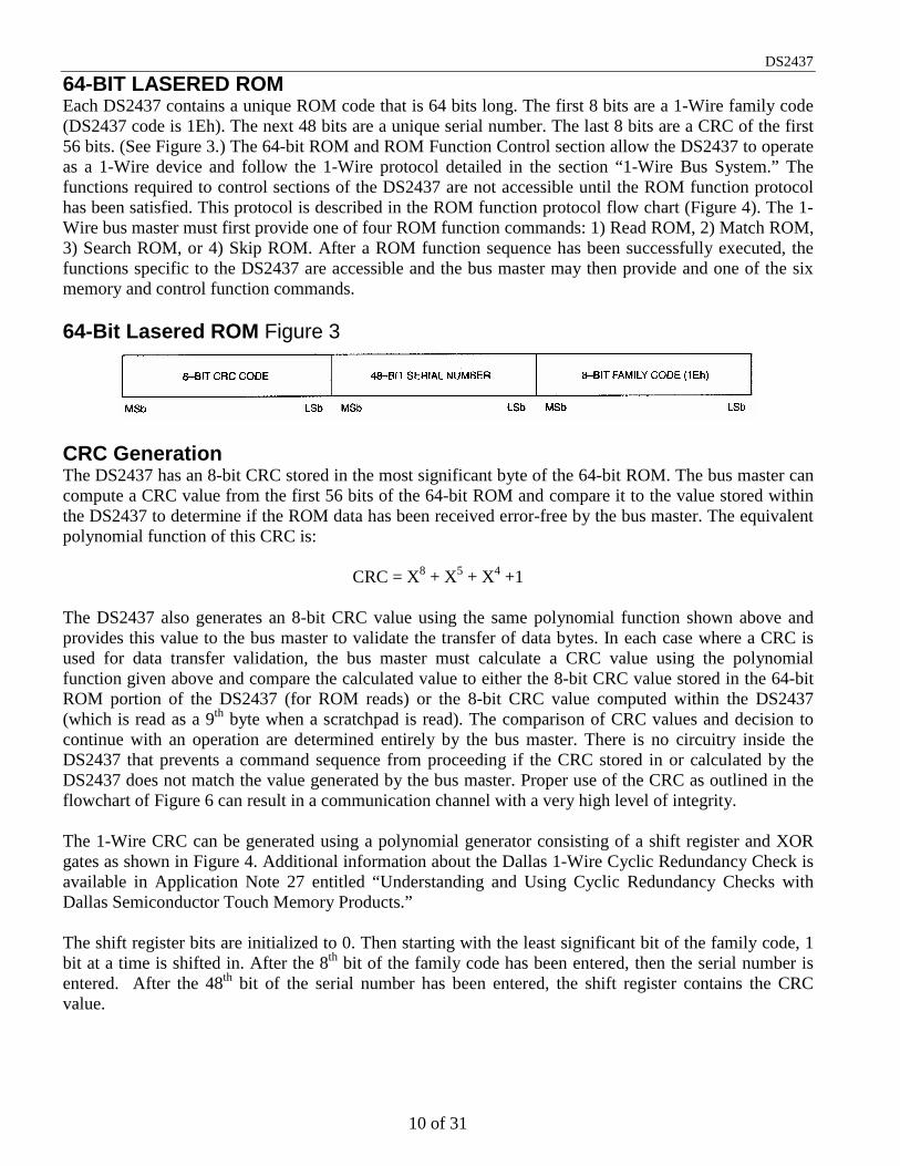
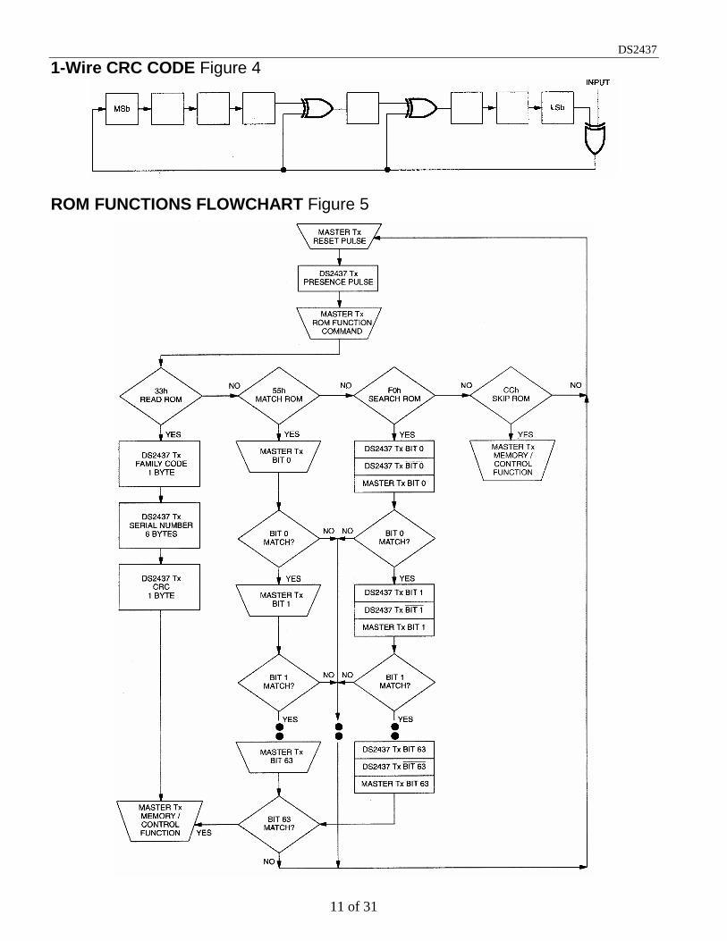
64-BIT LASERED ROMEach DS2437 contains a unique ROM code that is 64 bits long. The first 8 bits are a 1-Wire family code(DS2437 code is 1Eh). The next 48 bits are a unique serial number. The last 8 bits are a CRC of the first56 bits. (See Figure 3.) The 64-bit ROM and ROM Function Control section allow the DS2437 to operateas a 1-Wire device and follow the 1-Wire protocol detailed in the section “1-Wire Bus System.” Thefunctions required to control sections of the DS2437 are not accessible until the ROM function protocolhas been satisfied. This protocol is described in the ROM function protocol flow chart (Figure 4). The 1-Wire bus master must first provide one of four ROM function commands: 1) Read ROM, 2) Match ROM,3) Search ROM, or 4) Skip ROM. After a ROM function sequence has been successfully executed, thefunctions specific to the DS2437 are accessible and the bus master may then provide and one of the sixmemory and control function commands.
64-Bit Lasered ROM Figure 3
CRC GenerationThe DS2437 has an 8-bit CRC stored in the most significant byte of the 64-bit ROM. The bus master cancompute a CRC value from the first 56 bits of the 64-bit ROM and compare it to the value stored withinthe DS2437 to determine if the ROM data has been received error-free by the bus master. The equivalentpolynomial function of this CRC is:
CRC = X8 + X5 + X4 +1
The DS2437 also generates an 8-bit CRC value using the same polynomial function shown above andprovides this value to the bus master to validate the transfer of data bytes. In each case where a CRC isused for data transfer validation, the bus master must calculate a CRC value using the polynomialfunction given above and compare the calculated value to either the 8-bit CRC value stored in the 64-bitROM portion of the DS2437 (for ROM reads) or the 8-bit CRC value computed within the DS2437(which is read as a 9th byte when a scratchpad is read). The comparison of CRC values and decision tocontinue with an operation are determined entirely by the bus master. There is no circuitry inside theDS2437 that prevents a command sequence from proceeding if the CRC stored in or calculated by theDS2437 does not match the value generated by the bus master. Proper use of the CRC as outlined in theflowchart of Figure 6 can result in a communication channel with a very high level of integrity.
The 1-Wire CRC can be generated using a polynomial generator consisting of a shift register and XORgates as shown in Figure 4. Additional information about the Dallas 1-Wire Cyclic Redundancy Check isavailable in Application Note 27 entitled “Understanding and Using Cyclic Redundancy Checks withDallas Semiconductor Touch Memory Products.”
The shift register bits are initialized to 0. Then starting with the least significant bit of the family code, 1bit at a time is shifted in. After the 8th bit of the family code has been entered, then the serial number isentered. After the 48th bit of the serial number has been entered, the shift register contains the CRCvalue.
DS2437
11 of 31
1-Wire CRC CODE Figure 4
ROM FUNCTIONS FLOWCHART Figure 5
DS2437
12 of 31
MEMORY/CONTROL FUNCTIONS FLOWCHART Figure 6
YESNO
DS2437
13 of 31
MEMORY/CONTROL FUNCTIONS FLOWCHART Figure 6 Cont'd
DS2437 RECALLSEEPROM PAGEXINTO SP PAGEX
DS2437
14 of 31
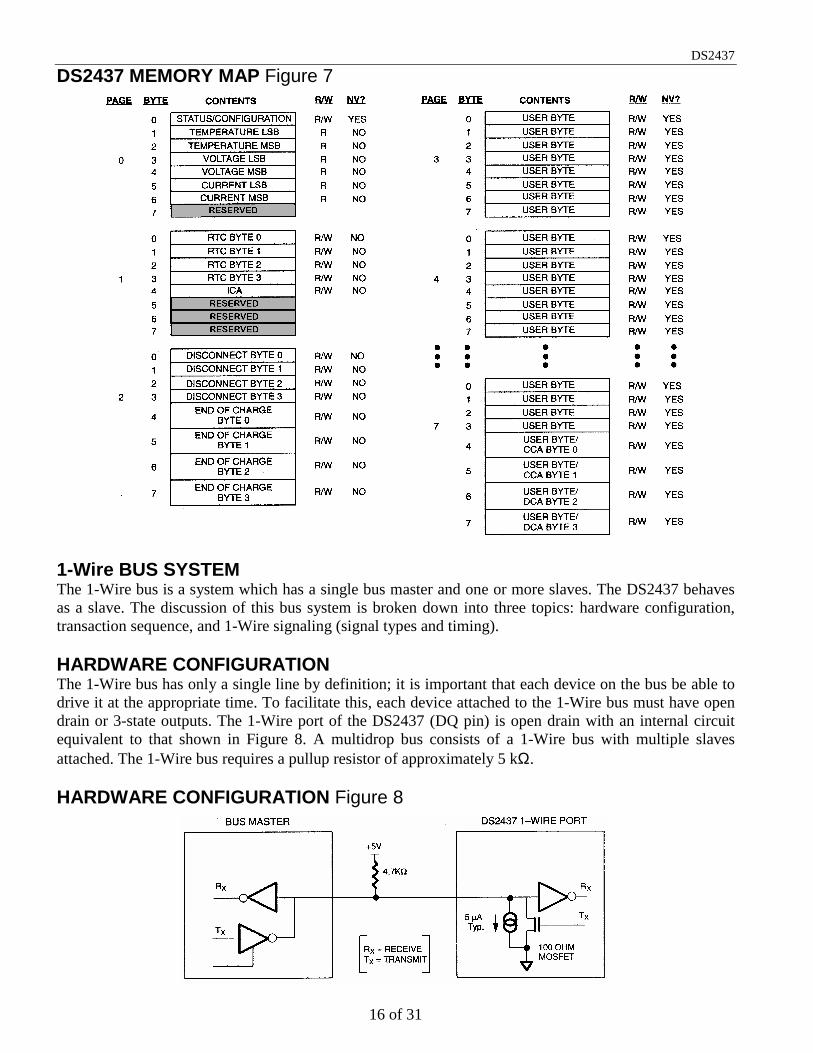
MEMORY MAPThe DS2437’s memory is organized as shown in Figure 7. The memory consists of a scratchpad RAMand storage SRAM/EEPROM. The scratchpad helps insure data integrity when communicating over the1-Wire bus. Data is first written to the scratchpad where it can be read back. After the data has beenverified, a copy scratchpad command will transfer the data to the appropriate page in memory (pages 0-2are primarily volatile SRAM, pages 3-7 are EEPROM). This process insures data integrity whenmodifying the memory.
The DS2437’s memory is organized as 64 bytes of memory in eight 8-byte pages. Each page has its ownscratchpad space, organized as 8 bytes of memory. When reading a scratchpad, there is a 9th byte whichmay be read with a Read Scratchpad command. This byte contains a cyclic redundancy check (CRC)byte, which is the CRC over all of the 8 bytes in the currently selected scratchpad. This CRC isimplemented in the fashion described in the section titled “CRC Generation.”
Page 0 (00h)The first page contains the most frequently accessed information of the DS2437, and most locations arevolatile read-only bytes with the exception of the Status / Configuration Register (Byte 0).
The Status / Configuration Register is a nonvolatile read/write byte which defines which features of theDS2437 are enabled and how they will function. The register is formatted as follows:
IAD = Current A/D Control Bit. 1 = the current A/D and the ICA are enabled, and current measurementswill be taken at the rate of 32 Hz; 0 = the current A/D and the ICA have been disabled.
CA = Current Accumulator Configuration. 1 = CCA/DCA are enabled, and data will be stored and can beretrieved from page 7, bytes 4-7; 0 = CCA/DCA is disabled, and page 7 can be used for generalEEPROM storage.
E2? = Current Accumulator Shadow Selector bit. 1 = CCA/DCA counter data will be shadowed toEEPROM each time the respective register is incremented by 0.32C; 0 = CCA/DCA counter data will notbe shadowed to EEPROM. The CCA/DCA could be lost as the battery pack becomes discharged. If theCA bit in the status/configuration register is set to 0, the E2? bit will have no effect on the DS2437functionality.
AD = Voltage A/D Input Select Bit. 1 = the battery input (VDD) is selected as the input for the DS2437voltage A/D converter; 0 = the general purpose A/D input (VAD) is selected as the voltage A/D input.For either setting, a Convert V command will initialize a voltage A/D conversion.
TB = Temperature Busy Flag. 1 = temperature conversion in progress; 0 = temperature conversioncomplete.
NVB = Nonvolatile Memory Busy Flag. 1 = Copy from Scratchpad to EEPROM in progress; 0 =Nonvolatile memory not busy. A copy to EEPROM may take from 2 ms to 10 ms (taking longer at lowersupply voltages).
DS2437
15 of 31
ADB = A/D Converter Busy Flag. 1 = A/D conversion in progress on battery voltage; 0 = conversioncomplete, or no measurement being made. An A/D conversion takes approximately 10 ms.
X = Don’t care
Bytes 1 and 2 of page 0 contain the last completed temperature conversion in the format described in the“Operation - Measuring Temperature” section. Bytes 3-4 contain the last completed voltage A/Dconversion result and Bytes 5-6 contain the instantaneous current data. Refer to the appropriate sectionfor the data format of these locations. Byte 7 is reserved and will read out as all 1’s.
Page 1 (01h)The second page, Page 1, contains the ICA and real time clock data. Both the RTC and ICA are volatileread/ write locations so that they may be set, changed, or cleared by the host software. Bytes 0-3 containthe RTC data, formatted as described in the “Operation - Real Time Clock” section. Byte 4 contains the8-bit ICA. Bytes 5-7 are reserved and will read out as all 1’s.
Page 2 (02h)The third page of memory (Page 2) contains the DISCONNECT TIME (first four bytes) and END OFCHARGE (remaining four bytes) timestamps. This page is volatile and read / write. Refer to the“Operation - Real Time Clock” section for the formatting of these locations.
Pages 3-7 (03h - 07h)The remainder of the memory in the DS2437 (Pages 3 through 7) is backed with EEPROM. This memoryprovides 40 bytes of user memory which may be used to carry any information the user wishes to store.Additionally, the CCA/DCA information is stored in bytes 4-7 of page 7 if the DS2437 is configuredappropriately. If the CCA/DCA is used, page 7 should not be written to or current accumulator data willbe overwritten. See “Operation - Current Accumulators” for details.
DS2437
16 of 31
DS2437 MEMORY MAP Figure 7
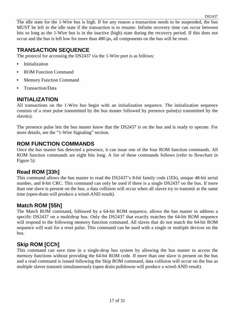
1-Wire BUS SYSTEMThe 1-Wire bus is a system which has a single bus master and one or more slaves. The DS2437 behavesas a slave. The discussion of this bus system is broken down into three topics: hardware configuration,transaction sequence, and 1-Wire signaling (signal types and timing).
HARDWARE CONFIGURATIONThe 1-Wire bus has only a single line by definition; it is important that each device on the bus be able todrive it at the appropriate time. To facilitate this, each device attached to the 1-Wire bus must have opendrain or 3-state outputs. The 1-Wire port of the DS2437 (DQ pin) is open drain with an internal circuitequivalent to that shown in Figure 8. A multidrop bus consists of a 1-Wire bus with multiple slavesattached. The 1-Wire bus requires a pullup resistor of approximately 5 kΩ.
HARDWARE CONFIGURATION Figure 8
DS2437
17 of 31
The idle state for the 1-Wire bus is high. If for any reason a transaction needs to be suspended, the busMUST be left in the idle state if the transaction is to resume. Infinite recovery time can occur betweenbits so long as the 1-Wire bus is in the inactive (high) state during the recovery period. If this does notoccur and the bus is left low for more than 480 µs, all components on the bus will be reset.
TRANSACTION SEQUENCEThe protocol for accessing the DS2437 via the 1-Wire port is as follows:
• Initialization
• ROM Function Command
• Memory Function Command
• Transaction/Data
INITIALIZATIONAll transactions on the 1-Wire bus begin with an initialization sequence. The initialization sequenceconsists of a reset pulse transmitted by the bus master followed by presence pulse(s) transmitted by theslave(s).
The presence pulse lets the bus master know that the DS2437 is on the bus and is ready to operate. Formore details, see the “1-Wire Signaling” section.
ROM FUNCTION COMMANDSOnce the bus master has detected a presence, it can issue one of the four ROM function commands. AllROM function commands are eight bits long. A list of these commands follows (refer to flowchart inFigure 5):
Read ROM [33h]This command allows the bus master to read the DS2437’s 8-bit family code (1Eh), unique 48-bit serialnumber, and 8-bit CRC. This command can only be used if there is a single DS2437 on the bus. If morethan one slave is present on the bus, a data collision will occur when all slaves try to transmit at the sametime (open-drain will produce a wired-AND result).
Match ROM [55h]The Match ROM command, followed by a 64-bit ROM sequence, allows the bus master to address aspecific DS2437 on a multidrop bus. Only the DS2437 that exactly matches the 64-bit ROM sequencewill respond to the following memory function command. All slaves that do not match the 64-bit ROMsequence will wait for a reset pulse. This command can be used with a single or multiple devices on thebus.
Skip ROM [CCh]This command can save time in a single-drop bus system by allowing the bus master to access thememory functions without providing the 64-bit ROM code. If more than one slave is present on the busand a read command is issued following the Skip ROM command, data collision will occur on the bus asmultiple slaves transmit simultaneously (open drain pulldowns will produce a wired-AND result).
DS2437
18 of 31
Search ROM [F0h]When a system is initially brought up, the bus master might not know the number of devices on the 1-Wire bus or their 64-bit ROM codes. The search ROM command allows the bus master to use a processof elimination to identify the 64-bit ROM codes of all slave devices on the bus.
Example of a ROM SearchThe ROM search process is the repetition of a simple three-step routine: read a bit, read the complementof the bit, then write the desired value of that bit. The bus master performs this simple, 3-step routine oneach bit of the ROM. After one complete pass, the bus master knows the contents of the ROM in onedevice. The remaining number of devices and their ROM codes may be identified by additional passes.
The following example of the ROM search process assumes four different devices are connected to thesame 1-Wire bus. The ROM data of the four devices is as shown (LSb first):
ROM1 = 00110101...ROM2 = 10101010...ROM3 = 11110101...ROM4 = 00010001...
The search process is as follows:1. The bus master begins the initialization sequence by issuing a reset pulse. The slave devices respond
by issuing simultaneous presence pulses.2. The bus master will then issue the search ROM command on the 1-Wire bus (F0h).3. The bus master reads a bit from the 1-Wire bus. Each device will respond by placing the value of the
first bit of their respective ROM data onto the 1-Wire bus. ROM1 and ROM4 will place a 0 onto the1-Wire bus, i.e., pull it low. ROM2 and ROM3 will place a 1 onto the 1-Wire bus by allowing the lineto stay high. The result is the logical AND of all devices on the line; therefore the bus master sees a 0.The bus master reads another bit. Since the Search ROM data command is being executed, all of thedevices on the 1-Wire bus respond to this second read by placing the complement of the first bit oftheir respective ROM data onto the 1-Wire bus. ROM1 and ROM4 will place a 1 onto the 1-wire,allowing the line to stay high. ROM2 and ROM3 will place a 0 onto the 1-wire; thus it will be pulledlow. The bus master again observes a 0 for the complement of the first ROM data bit. The bus masterhas determined that there are some devices on the 1-Wire bus that have a 0 in the first position andothers that have a 1.The data obtained from the two reads of the three-step routine have the following interpretations:00 - There are still devices attached which have conflicting bits in this position.01 - All devices still coupled have a 0-bit in this bit position.10 - All devices still coupled have a 1-bit in this bit position.11 - There are no devices attached to the 1-Wire bus.
4. The bus master writes a 0. This deselects ROM2 and ROM3 for the remainder of this search pass,leaving only ROM1 and ROM4 connected to the 1-Wire bus.
5. The bus master performs two more reads and receives a 0-bit followed by a 1-bit. This indicates thatall devices still coupled to the bus have 0s as their second ROM data bit.
6. The bus master then writes a 0 to keep both ROM1 and ROM4 coupled.7. The bus master executes two reads and receives two 0-bits. This indicates that both 1-bits and 0-bits
exist as the 3rd bit of the ROM data of the attached devices.
DS2437
19 of 31
8. The bus master writes a 0-bit. This deselects ROM1 leaving ROM4 as the only device still connected.9. The bus master reads the remainder of the ROM bits for ROM4 and continues to access the part if
desired. This completes the first pass and uniquely identifies one part on the 1-Wire bus.10. The bus master starts a new ROM search sequence by repeating steps 1 through 7.11. The bus master writes a 1-bit. This decouples ROM4, leaving only ROM1 still coupled.12. The bus master reads the remainder of the ROM bits for ROM1 and communicates to the underlying
logic if desired. This completes the second ROM search pass, in which another of the ROMs wasfound.
13. The bus master starts a new ROM search by repeating steps 1 through 3.14. The bus master writes a 1-bit. This deselects ROM1 and ROM4 for the remainder of this search pass,
leaving only ROM2 and ROM3 coupled to the system.15. The bus master executes two read time slots and receives two 0s.16. The bus master writes a 0-bit. This decouples ROM3, and leaving only ROM2.17. The bus master reads the remainder of the ROM bits for ROM2 and communicates to the underlying
logic if desired. This completes the third ROM search pass, in which another of the ROMs was found.18. The bus master starts a new ROM search by repeating steps 13 through 15.19. The bus master writes a 1-bit. This decouples ROM2, leaving only ROM3.20. The bus master reads the remainder of the ROM bits for ROM3 and communicates to the underlying
logic if desired. This completes the fourth ROM search pass, in which another of the ROMs wasfound.
Note that the bus master learns the unique ID number (ROM data pattern) of one 1-Wire device on eachROM Search operation. The time required to derive the part’s unique ROM code is:
960 µs + (8 + 3 x 64) 61 µs = 13.16 msThe bus master is therefore capable of identifying 75 different 1-Wire devices per second.
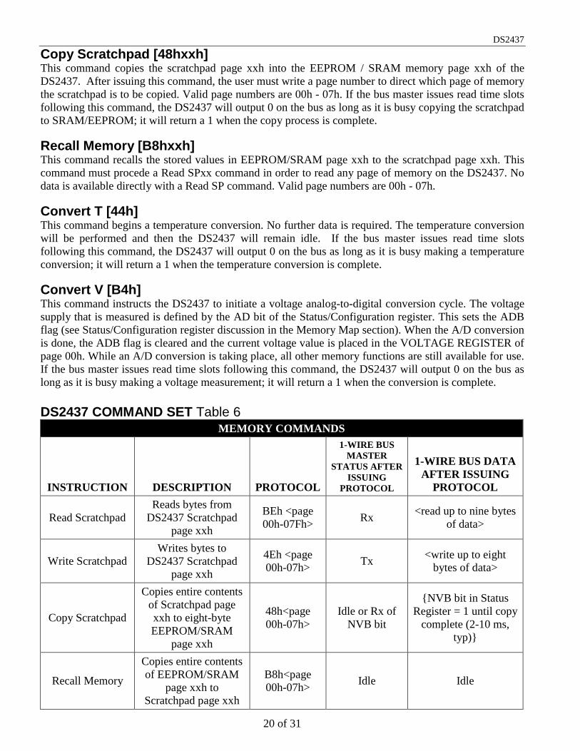
MEMORY COMMAND FUNCTIONSThe following command protocols are summarized in Table 6, and by the flowchart of Figure 6.
Write Scratchpad [4Ehxxh]This command writes to the scratchpad page xxh of the DS2437. The entire 8-byte scratchpad space maybe written, but all writing begins with the byte present at address 0 of the selected scratchpad. Afterissuing this command, the user must send the page number of the scratchpad to be written; then the usermay begin writing data to the DS2437 scratchpad. Writing may be terminated at any point by issuing areset. Valid page numbers for writing are 00h-07h.
Read Scratchpad [BEhxxh]This command reads the contents of the scratchpad page xxh on the DS2437. After issuing this command,the user must send the page number of the scratchpad to be read, and then may begin reading the data,always beginning at address 0 of the selected scratchpad. The user may read through the end of thescratchpad space (byte 07h), with any reserved data bits reading all logic 1s and after which the data readwill be all logic 1s. If not all locations are to be read, the master may issue a reset to terminate reading atany time. Valid page numbers are 00h - 07h.
DS2437
20 of 31
Copy Scratchpad [48hxxh]This command copies the scratchpad page xxh into the EEPROM / SRAM memory page xxh of theDS2437. After issuing this command, the user must write a page number to direct which page of memorythe scratchpad is to be copied. Valid page numbers are 00h - 07h. If the bus master issues read time slotsfollowing this command, the DS2437 will output 0 on the bus as long as it is busy copying the scratchpadto SRAM/EEPROM; it will return a 1 when the copy process is complete.
Recall Memory [B8hxxh]This command recalls the stored values in EEPROM/SRAM page xxh to the scratchpad page xxh. Thiscommand must procede a Read SPxx command in order to read any page of memory on the DS2437. Nodata is available directly with a Read SP command. Valid page numbers are 00h - 07h.
Convert T [44h]This command begins a temperature conversion. No further data is required. The temperature conversionwill be performed and then the DS2437 will remain idle. If the bus master issues read time slotsfollowing this command, the DS2437 will output 0 on the bus as long as it is busy making a temperatureconversion; it will return a 1 when the temperature conversion is complete.
Convert V [B4h]This command instructs the DS2437 to initiate a voltage analog-to-digital conversion cycle. The voltagesupply that is measured is defined by the AD bit of the Status/Configuration register. This sets the ADBflag (see Status/Configuration register discussion in the Memory Map section). When the A/D conversionis done, the ADB flag is cleared and the current voltage value is placed in the VOLTAGE REGISTER ofpage 00h. While an A/D conversion is taking place, all other memory functions are still available for use.If the bus master issues read time slots following this command, the DS2437 will output 0 on the bus aslong as it is busy making a voltage measurement; it will return a 1 when the conversion is complete.
DS2437 COMMAND SET Table 6MEMORY COMMANDS
INSTRUCTION DESCRIPTION PROTOCOL
1-WIRE BUSMASTER
STATUS AFTERISSUING
PROTOCOL
1-WIRE BUS DATAAFTER ISSUING
PROTOCOL
Read ScratchpadReads bytes from
DS2437 Scratchpadpage xxh
BEh <page00h-07Fh> Rx <read up to nine bytes
of data>
Write ScratchpadWrites bytes to
DS2437 Scratchpadpage xxh
4Eh <page00h-07h> Tx <write up to eight
bytes of data>
Copy Scratchpad
Copies entire contentsof Scratchpad pagexxh to eight-byteEEPROM/SRAM
page xxh
48h<page00h-07h>
Idle or Rx ofNVB bit
NVB bit in StatusRegister = 1 until copy
complete (2-10 ms,typ)
Recall Memory
Copies entire contentsof EEPROM/SRAM
page xxh toScratchpad page xxh
B8h<page00h-07h> Idle Idle
DS2437
21 of 31
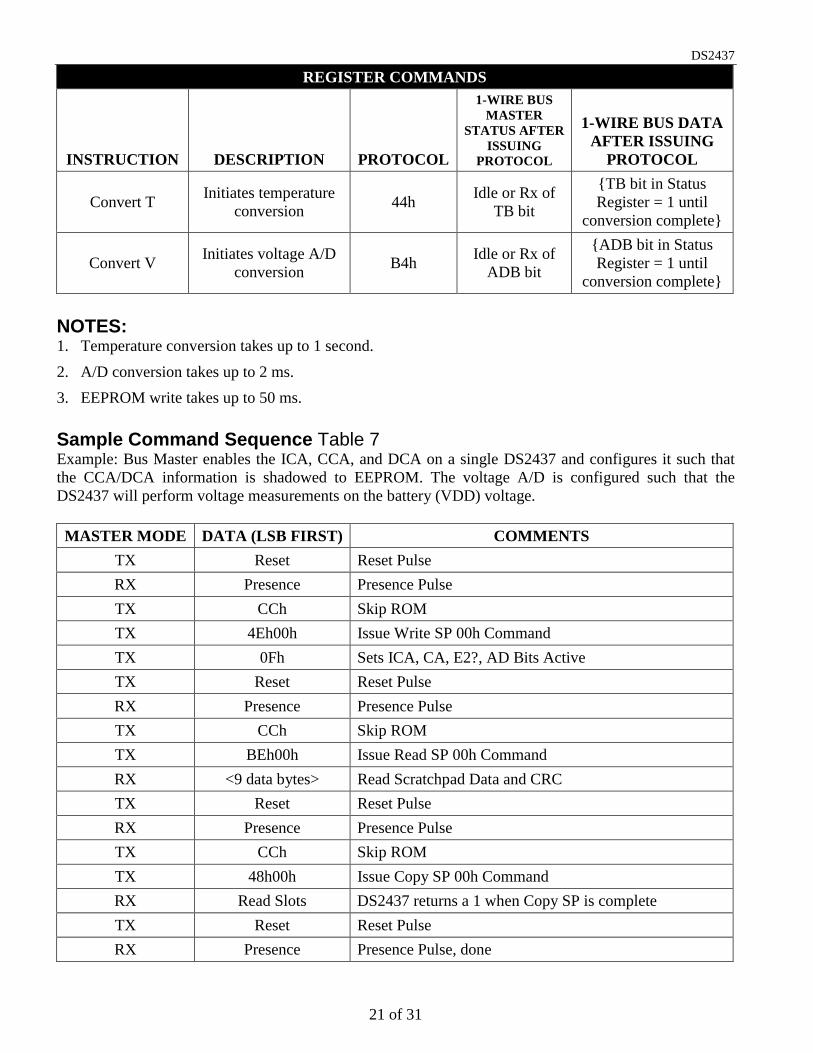
REGISTER COMMANDS
INSTRUCTION DESCRIPTION PROTOCOL
1-WIRE BUSMASTER
STATUS AFTERISSUING
PROTOCOL
1-WIRE BUS DATAAFTER ISSUING
PROTOCOL
Convert T Initiates temperatureconversion 44h Idle or Rx of
TB bit
TB bit in StatusRegister = 1 until
conversion complete
Convert V Initiates voltage A/Dconversion B4h Idle or Rx of
ADB bit
ADB bit in StatusRegister = 1 until
conversion complete
NOTES:1. Temperature conversion takes up to 1 second.2. A/D conversion takes up to 2 ms.3. EEPROM write takes up to 50 ms.
Sample Command Sequence Table 7Example: Bus Master enables the ICA, CCA, and DCA on a single DS2437 and configures it such thatthe CCA/DCA information is shadowed to EEPROM. The voltage A/D is configured such that theDS2437 will perform voltage measurements on the battery (VDD) voltage.
MASTER MODE DATA (LSB FIRST) COMMENTSTX Reset Reset PulseRX Presence Presence PulseTX CCh Skip ROMTX 4Eh00h Issue Write SP 00h CommandTX 0Fh Sets ICA, CA, E2?, AD Bits ActiveTX Reset Reset PulseRX Presence Presence PulseTX CCh Skip ROMTX BEh00h Issue Read SP 00h CommandRX <9 data bytes> Read Scratchpad Data and CRCTX Reset Reset PulseRX Presence Presence PulseTX CCh Skip ROMTX 48h00h Issue Copy SP 00h CommandRX Read Slots DS2437 returns a 1 when Copy SP is completeTX Reset Reset PulseRX Presence Presence Pulse, done
DS2437
22 of 31
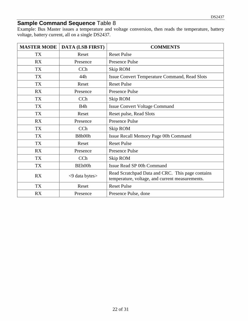
Sample Command Sequence Table 8Example: Bus Master issues a temperature and voltage conversion, then reads the temperature, batteryvoltage, battery current, all on a single DS2437.
MASTER MODE DATA (LSB FIRST) COMMENTSTX Reset Reset PulseRX Presence Presence PulseTX CCh Skip ROMTX 44h Issue Convert Temperature Command, Read SlotsTX Reset Reset PulseRX Presence Presence PulseTX CCh Skip ROMTX B4h Issue Convert Voltage CommandTX Reset Reset pulse, Read SlotsRX Presence Presence PulseTX CCh Skip ROMTX B8h00h Issue Recall Memory Page 00h CommandTX Reset Reset PulseRX Presence Presence PulseTX CCh Skip ROMTX BEh00h Issue Read SP 00h Command
RX <9 data bytes> Read Scratchpad Data and CRC. This page containstemperature, voltage, and current measurements.
TX Reset Reset PulseRX Presence Presence Pulse, done
DS2437
23 of 31
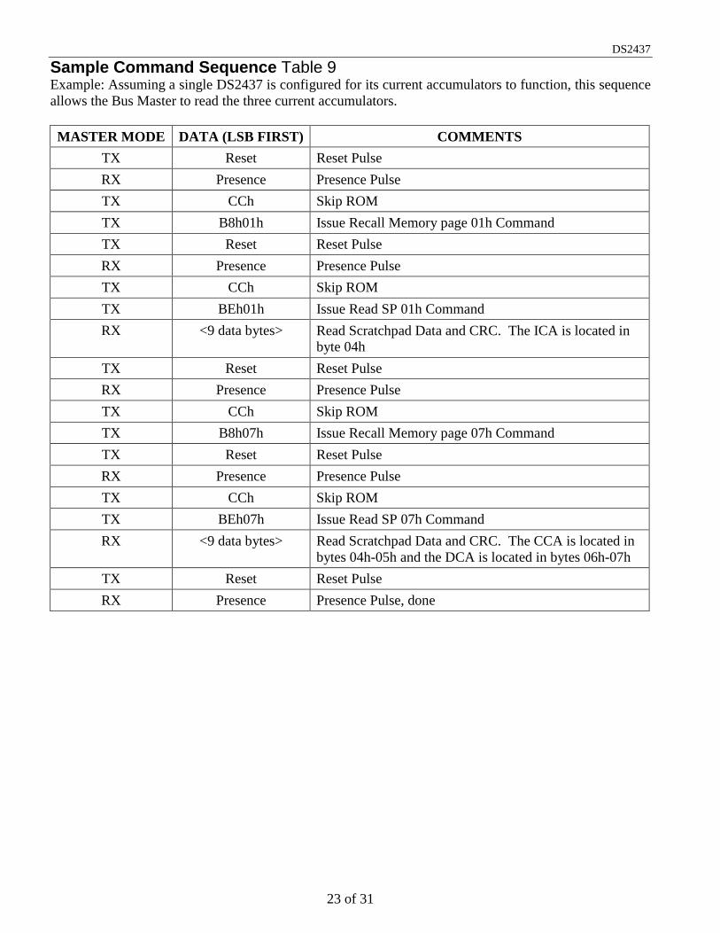
Sample Command Sequence Table 9Example: Assuming a single DS2437 is configured for its current accumulators to function, this sequenceallows the Bus Master to read the three current accumulators.
MASTER MODE DATA (LSB FIRST) COMMENTSTX Reset Reset PulseRX Presence Presence PulseTX CCh Skip ROMTX B8h01h Issue Recall Memory page 01h CommandTX Reset Reset PulseRX Presence Presence PulseTX CCh Skip ROMTX BEh01h Issue Read SP 01h CommandRX <9 data bytes> Read Scratchpad Data and CRC. The ICA is located in
byte 04hTX Reset Reset PulseRX Presence Presence PulseTX CCh Skip ROMTX B8h07h Issue Recall Memory page 07h CommandTX Reset Reset PulseRX Presence Presence PulseTX CCh Skip ROMTX BEh07h Issue Read SP 07h CommandRX <9 data bytes> Read Scratchpad Data and CRC. The CCA is located in
bytes 04h-05h and the DCA is located in bytes 06h-07hTX Reset Reset PulseRX Presence Presence Pulse, done
DS2437
24 of 31
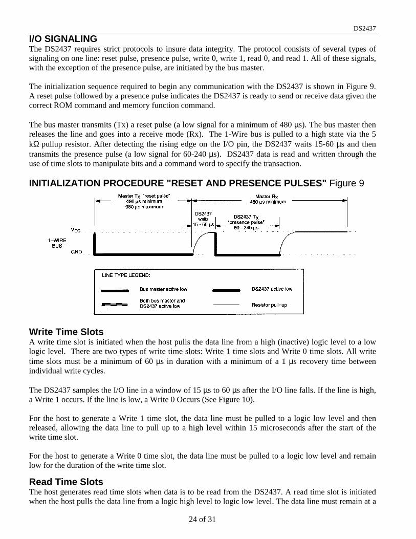
I/O SIGNALINGThe DS2437 requires strict protocols to insure data integrity. The protocol consists of several types ofsignaling on one line: reset pulse, presence pulse, write 0, write 1, read 0, and read 1. All of these signals,with the exception of the presence pulse, are initiated by the bus master.
The initialization sequence required to begin any communication with the DS2437 is shown in Figure 9.A reset pulse followed by a presence pulse indicates the DS2437 is ready to send or receive data given thecorrect ROM command and memory function command.
The bus master transmits (Tx) a reset pulse (a low signal for a minimum of 480 µs). The bus master thenreleases the line and goes into a receive mode (Rx). The 1-Wire bus is pulled to a high state via the 5kΩ=pullup resistor. After detecting the rising edge on the I/O pin, the DS2437 waits 15-60 µs and thentransmits the presence pulse (a low signal for 60-240 µs). DS2437 data is read and written through theuse of time slots to manipulate bits and a command word to specify the transaction.
INITIALIZATION PROCEDURE "RESET AND PRESENCE PULSES" Figure 9
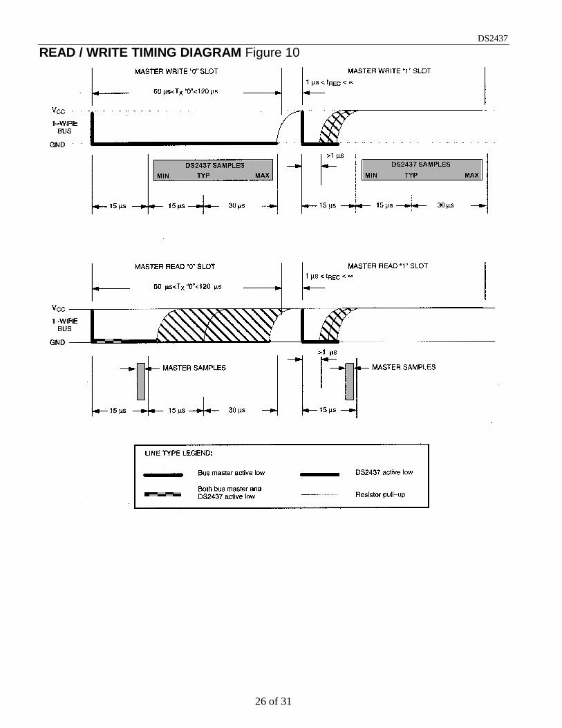
Write Time SlotsA write time slot is initiated when the host pulls the data line from a high (inactive) logic level to a lowlogic level. There are two types of write time slots: Write 1 time slots and Write 0 time slots. All writetime slots must be a minimum of 60 µs in duration with a minimum of a 1 µs recovery time betweenindividual write cycles.
The DS2437 samples the I/O line in a window of 15 µs to 60 µs after the I/O line falls. If the line is high,a Write 1 occurs. If the line is low, a Write 0 Occurs (See Figure 10).
For the host to generate a Write 1 time slot, the data line must be pulled to a logic low level and thenreleased, allowing the data line to pull up to a high level within 15 microseconds after the start of thewrite time slot.
For the host to generate a Write 0 time slot, the data line must be pulled to a logic low level and remainlow for the duration of the write time slot.
Read Time SlotsThe host generates read time slots when data is to be read from the DS2437. A read time slot is initiatedwhen the host pulls the data line from a logic high level to logic low level. The data line must remain at a
DS2437
25 of 31
low logic level for a minimum of 1 µs; output data from the DS2437 is then valid within the next 14 µsmaximum.
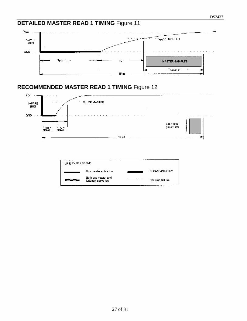
The host therefore must stop driving the I/O pin low in order to read its state 15 µs from the start of theread slot. (see Figure 10). By the end of the read time slot, the I/O pin will pull back high via the externalpullup resistor. All read time slots must be a minimum of 60 µs in duration with a minimum of a 1 µsrecovery time between individual read slots. Figure 11 shows that the sum of tINIT, tRC, and tSAMPLE mustbe less than 15 µs. Figure 12 shows that system timing margin is maximized by keeping tINIT, and tRC assmall as possible and by locating the master sample time toward the end of the 15 µs period.
RELATED APPLICATIONS NOTESThe following Application Notes can be applied to the DS2437. These notes can be obtained from theDallas Semiconductor Application Note Book, via our website at http://www.dalsemi.com, or through ourfaxback service at (972) 371-4441.
Application Note 27: “Understanding and Using Cyclic Redundancy Checks with Dallas SemiconductorTouch Memory Product”
Application Note 74: “Reading and Writing Touch Memories via Serial Interfaces”
Application Note 110: “NiCd/NiMH Intelligent Battery System Reference Design Using the DS2437”
Sample 1-Wire subroutines that can be used in conjunction with AN74 can be downloaded from thewebsite.
DS2437
26 of 31
READ / WRITE TIMING DIAGRAM Figure 10
DS2437
27 of 31
DETAILED MASTER READ 1 TIMING Figure 11
RECOMMENDED MASTER READ 1 TIMING Figure 12
DS2437
28 of 31
ABSOLUTE MAXIMUM RATINGS*Voltage on VDD and VAD, Relative to Ground -0.3V to +12VVoltage on VSENS+, VSENS-, Relative to Ground >±300 mVVoltage on Any Pin Relative to Ground -0.3V to +7.0VOperating Temperature -40°C to +85°CStorage Temperature -55°C to +125°CSoldering Temperature 260°C for 10 seconds
* This is a stress rating only and functional operation of the device at these or any other conditionsabove those indicated in the operation sections of this specification is not implied. Exposure toabsolute maximum rating conditions for extended periods of time may affect reliability.
RECOMMENDED DCOPERATING CONDITIONS (-40°C to +85°C; 2.7V ≤ VDD ≤ 10.0V)PARAMETER SYMBOL CONDITION MIN TYP MAX UNITS NOTESSupply Voltage VDD 2.7 10.0 V 3Data Pin DQ -0.3 +5.5 V 3DQ Pullup Voltage 2.7 5.5Analog Ground AGND GND
-0.5GND+0.5
V 3
DC ELECTRICAL CHARACTERISTICS (-40°C to +85°C; 2.7V ≤ VDD ≤ 10.0V)PARAMETER SYMBOL CONDITION MIN TYP MAX UNITS NOTESInput Logic High VIH 2.0 V 3Input Logic Low VIL -0.3 0.8 V 3Shutdown Current IDD1 DQ=0, RTC
Active10 15 µA 2, 4
Standby Current IDD2 DQ=1, ICAActive
50 100 µA 2, 4
Active Current IDD Temperature orVoltage
Conversions orEEPROM write
in progress
250 1000 µA 4
Input Resistance RI DQ 500 kΩ 5
ELECTRICAL CHARACTERISTICS:DIGITAL THERMOMETER (-40°C to +85°C; 2.7V ≤ VDD ≤ 10.0V)PARAMETER SYMBOL CONDITION MIN TYP MAX UNITS NOTESThermometer Error(TACTUAL - TMEASURED)
TERR 0°C to 70°C ±2 °C 6
Resolution 13 bitsConversion Time tCONVT 400 1000 ms
DS2437
29 of 31
ELECTRICAL CHARACTERISTICS:VOLTAGE A/D CONVERTER (-40°C to +85°C; 2.7V ≤ VDD ≤ 10.0V)PARAMETER SYMBOL CONDITION MIN TYP MAX UNITS NOTESA/D Error VADERR ±10 ±50 mVVAD Input Range VADR 2.7V ≤ VDD ≤
5.0V0 2VDD V 3
VAD Input Range VADR1 VDD > 5.0V 0 10.0 V 3VDD Input Range VDDR 2.7 10.0 V 3Resolution 10 bitsConversion Time tCONVV 2 msNo Missing CodeTemperature Range
-40 +85 °C
Monotonicity Guaranteed
ELECTRICAL CHARACTERISTICS:CURRENT A/D CONVERTER (-40°C to +85°C; 4.5V ≤ VDD ≤ 10.0V)PARAMETER SYMBOL CONDITION MIN TYP MAX UNITS NOTESCurrent MeasurementError
IADERR ±2 LSB 1
Integrated CurrentError
CAERR 2 5 %
Instantaneous CurrentResolution
10 bits
ELECTRICAL CHARACTERISTICS:RTC COUNTER (-40°C to +85°C; 2.7V ≤ VDD ≤ 10.0V)PARAMETER SYMBOL CONDITION MIN TYP MAX UNITS NOTESClock Error RTCERR 6Resolution 1 sec
DS2437
30 of 31
AC ELECTRICAL CHARACTERISTICS:1-WIRE INTERFACE (-40°C to +85°C; 2.7V ≤ VDD ≤ 10.0V)PARAMETER SYMBOL CONDITION MIN TYP MAX UNITS NOTESTime Slot tSLOT 60 120 µsRecovery Time tREC 1 µsWrite 0 Low Time tLOW0 60 120 µsWrite 1 Low Time tLOW1 1 15 µsRead Data Valid tRDV 15 µsReset Time High tRSTH 480 µsReset Time Low tRSTL 480 µsPresence Detect High tPDH 15 60 µs
PARAMETER SYMBOL CONDITION MIN TYP MAX UNITS NOTESPresence Detect Low tPDL 60 240 µsDQ Capacitance CDQ 25 pF
NOTES:1. Current measurement accuracy is ±2 LSb or 2%, whichever is greater. Contact the factory for
applications with less than 4.5V supply voltage.2. Shutdown and Standby currents specified for the range 0°C to 70°C.3. All Voltages are referenced to GND.4. IDD specified with VDD = 5.0V.5. Input load is to GND.6. Refer to Application Note 58.7. See Figure 13 for internal ground connections. GND and AGND must be connected to the same
potential.
INTERNAL GROUND CONNECTIONS Figure 13
DS2437
31 of 31
TIMING DIAGRAMS Figure 14
1-WIRE WRITE 1 TIME SLOT
1-WIRE WRITE 0 TIME SLOT
1-WIRE READ TIME SLOT
1-WIRE RESET PULSE
1-WIRE PRESENCE DETECT