Embed Size (px)
Citation preview

T4086
Analog MEMS Microphone
TDK reserves the right to change the detail specifications as may be required to permit improvements in the design of its products.
TDK Corporation 1745 Technology Drive, San Jose, CA 95110 U.S.A
+1(408) 988–7339 www.tdk.com
Document Number: DS‐000365 Revision: 1.1 Release Date: 11/19/2020
GENERAL DESCRIPTION The T4086 is an analog MEMS microphone with high SNR in small package size. The T4086 includes a MEMS microphone element, an impedance converter, and an output amplifier. Other high‐performance specifications include 127 dB SPL acoustic overload point, tight ±1 dB sensitivity tolerance and enhanced immunity to both radiated and conducted RF interference. The T4086 is available in a small 2.75 mm × 1.85 mm × 0.9 mm bottom port surface‐mount package.
APPLICATIONS Mobile phones Headsets Still and video cameras IoT devices
FEATURES
SPEC PERFORMANCE SNR 62 dBA
Current 140 µA
AOP 127 SPL
Single ended, non‐inverting analog output −38 dBV sensitivity ±1 dB sensitivity tolerance Frequency response from 95 Hz to 20 kHz Enhanced RF immunity −98 dBV(A) PSRR 2.75 × 1.85 × 0.9 mm surface‐mount package Compatible with Pb‐free solder processes RoHS compliant
FUNCTIONAL BLOCK DIAGRAM
ORDERING INFORMATION
PART TEMP RANGE PACKAGING MMICT4086‐00‐908 ‐40°C to +85°C 330mm Tape and Reel
EV_T4086‐FX —
T4086
Page 2 of 15 Document Number: DS‐000365 Revision: 1.1
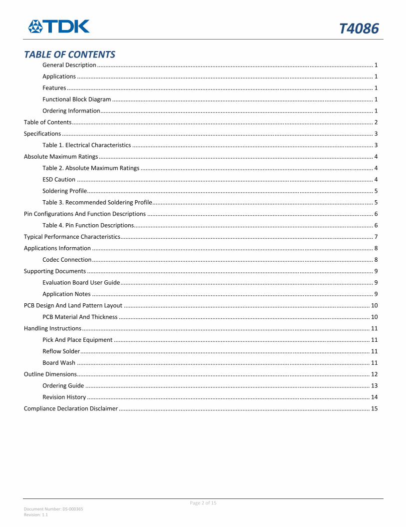
TABLE OF CONTENTS General Description ..................................................................................................................................................................... 1
Applications ................................................................................................................................................................................. 1
Features ....................................................................................................................................................................................... 1
Functional Block Diagram ............................................................................................................................................................ 1
Ordering Information ................................................................................................................................................................... 1
Table of Contents .................................................................................................................................................................................... 2
Specifications .......................................................................................................................................................................................... 3
Table 1. Electrical Characteristics ................................................................................................................................................ 3
Absolute Maximum Ratings .................................................................................................................................................................... 4
Table 2. Absolute Maximum Ratings ........................................................................................................................................... 4
ESD Caution ................................................................................................................................................................................. 4
Soldering Profile ........................................................................................................................................................................... 5
Table 3. Recommended Soldering Profile .................................................................................................................................... 5
Pin Configurations And Function Descriptions ....................................................................................................................................... 6
Table 4. Pin Function Descriptions ............................................................................................................................................... 6
Typical Performance Characteristics ....................................................................................................................................................... 7
Applications Information ........................................................................................................................................................................ 8
Codec Connection ........................................................................................................................................................................ 8
Supporting Documents ........................................................................................................................................................................... 9
Evaluation Board User Guide ....................................................................................................................................................... 9
Application Notes ........................................................................................................................................................................ 9
PCB Design And Land Pattern Layout ................................................................................................................................................... 10
PCB Material And Thickness ...................................................................................................................................................... 10
Handling Instructions ............................................................................................................................................................................ 11
Pick And Place Equipment ......................................................................................................................................................... 11
Reflow Solder ............................................................................................................................................................................. 11
Board Wash ............................................................................................................................................................................... 11
Outline Dimensions ............................................................................................................................................................................... 12
Ordering Guide .......................................................................................................................................................................... 13
Revision History ......................................................................................................................................................................... 14
Compliance Declaration Disclaimer ...................................................................................................................................................... 15

T4086
Page 3 of 15 Document Number: DS‐000365 Revision: 1.1
SPECIFICATIONS TABLE 1. ELECTRICAL CHARACTERISTICS TA = 25°C, VDD = 1.8 V, unless otherwise noted. Typical specifications are not guaranteed.
PARAMETER CONDITIONS MIN TYP MAX UNITS NOTES
PERFORMANCE
Directionality Omni
Output Polarity Non‐Inverted
Sensitivity 1 kHz, 94 dB SPL −39 −38 −37 dBV
Signal‐to‐Noise Ratio (SNR) 20 kHz bandwidth, A‐weighted 60 62 dBA
Equivalent Input Noise (EIN) 20 kHz bandwidth, A‐weighted 32 dBA SPL
Dynamic Range Derived from EIN and acoustic overload point
95 dB
Total Harmonic Distortion (THD) 115 dB SPL, 1kHz 1 2 %
Power Supply Rejection Ratio (PSRR) 1 kHz, 200 mV p‐p sine wave superimposed on VDD = 1.8 V
65 75 dB
Power Supply Rejection (PSR) 217 Hz, 200 mV p‐p square wave superimposed on VDD = 1.8 V
−98 dBV(A)
Acoustic Overload Point 10% THD 127 dB SPL
POWER SUPPLY
Supply Voltage (VDD) Standard mode 1.6 3.6 V
Supply Current (IS) VDD = 1.8 V 140 160 µA
OUTPUT CHARACTERISTICS
Output Impedance 250 Ω
Output DC voltage 740 mV
Startup Time Output to within ±0.5 dB of stable sensitivity
30 ms
T4086
Page 4 of 15 Document Number: DS‐000365 Revision: 1.1
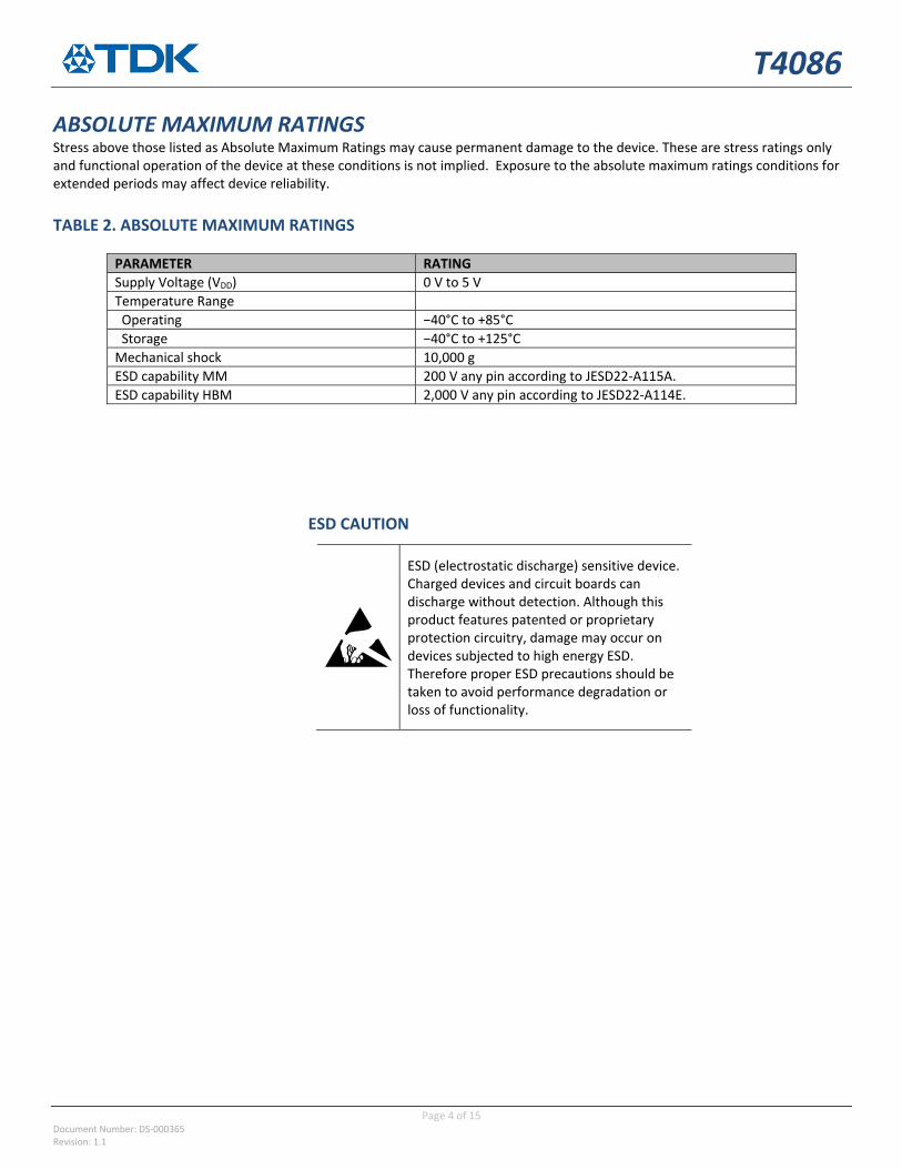
ABSOLUTE MAXIMUM RATINGS Stress above those listed as Absolute Maximum Ratings may cause permanent damage to the device. These are stress ratings only and functional operation of the device at these conditions is not implied. Exposure to the absolute maximum ratings conditions for extended periods may affect device reliability.
TABLE 2. ABSOLUTE MAXIMUM RATINGS
PARAMETER RATING
Supply Voltage (VDD) 0 V to 5 V
Temperature Range
Operating −40°C to +85°C
Storage −40°C to +125°C
Mechanical shock 10,000 g
ESD capability MM 200 V any pin according to JESD22‐A115A.
ESD capability HBM 2,000 V any pin according to JESD22‐A114E.
ESD CAUTION
ESD (electrostatic discharge) sensitive device. Charged devices and circuit boards can discharge without detection. Although this product features patented or proprietary protection circuitry, damage may occur on devices subjected to high energy ESD. Therefore proper ESD precautions should be taken to avoid performance degradation or loss of functionality.

T4086
Page 5 of 15 Document Number: DS‐000365 Revision: 1.1
SOLDERING PROFILE
Figure 1. Recommended Soldering Profile Limits
TABLE 3. RECOMMENDED SOLDERING PROFILE
PROFILE FEATURE Pb‐Free
Ramp rate ≤ 3 K/s
Preheat 125°C to 220°C, 150 s to 210 s, 0.4 K/s to 1.0 K/s
T > 220°C 30 s to 70 s
T > 230°C Min. 10 s
T > 245°C Max. 20 s
T ≥ 255°C −
Peak temperature Tpeak 250°C +0/‐5°C
Wetting temperature Tmin 230°C +5/‐0°C for 10 s ± 1 s
Cooling rate ≤ 3 K/s
Soldering temperature T Measured at solder pads
0
40
80
120
160
200
240
280
0 60 120 180 240 300 360 420
time (sec)
tem
pera
ture
(°C
)
max. recomm. tempreflow soldering
min. temp for wetting

T4086
Page 6 of 15 Document Number: DS‐000365 Revision: 1.1
PIN CONFIGURATIONS AND FUNCTION DESCRIPTIONS
Figure 2. Pin Configuration (Top View, Terminal Side Down)
TABLE 4. PIN FUNCTION DESCRIPTIONS
PIN NAME FUNCTION
1 OUT Output
2 KOA keep out area, no structure on PCB recommended
3 GND Ground
4 KOA keep out area, no structure on PCB recommended
5 VDD Supply Voltage
T4086
Page 7 of 15 Document Number: DS‐000365 Revision: 1.1
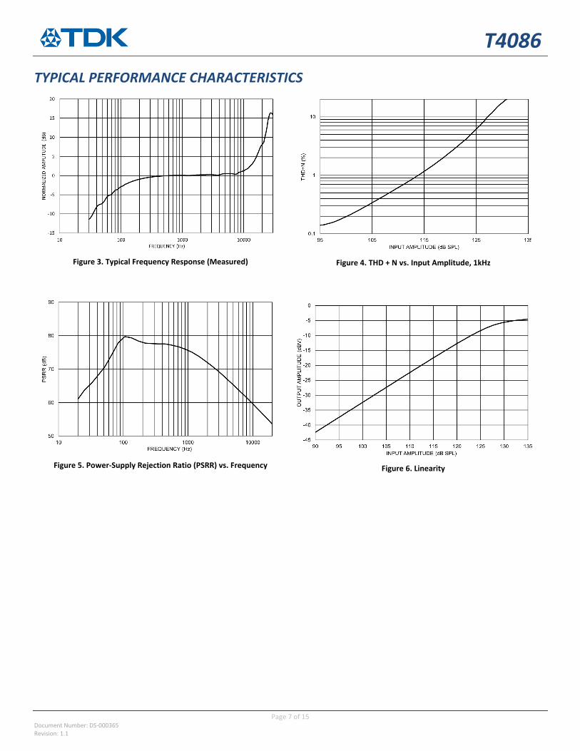
TYPICAL PERFORMANCE CHARACTERISTICS
Figure 3. Typical Frequency Response (Measured)
Figure 4. THD + N vs. Input Amplitude, 1kHz
Figure 5. Power‐Supply Rejection Ratio (PSRR) vs. Frequency
Figure 6. Linearity
T4086
Page 8 of 15 Document Number: DS‐000365 Revision: 1.1
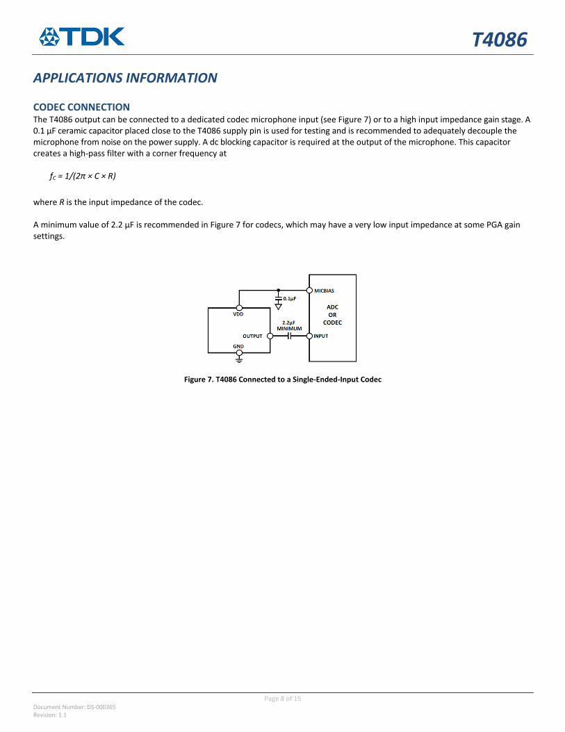
APPLICATIONS INFORMATION CODEC CONNECTION The T4086 output can be connected to a dedicated codec microphone input (see Figure 7) or to a high input impedance gain stage. A 0.1 µF ceramic capacitor placed close to the T4086 supply pin is used for testing and is recommended to adequately decouple the microphone from noise on the power supply. A dc blocking capacitor is required at the output of the microphone. This capacitor creates a high‐pass filter with a corner frequency at
fC = 1/(2π × C × R)
where R is the input impedance of the codec. A minimum value of 2.2 μF is recommended in Figure 7 for codecs, which may have a very low input impedance at some PGA gain settings.
Figure 7. T4086 Connected to a Single‐Ended‐Input Codec

T4086
Page 9 of 15 Document Number: DS‐000365 Revision: 1.1
SUPPORTING DOCUMENTS For additional information, see the following documents.
EVALUATION BOARD USER GUIDE AN‐000013, Analog Output MEMS Microphone Flex Evaluation Board User Guide
APPLICATION NOTES AN‐100, MEMS Microphone Handling and Assembly Guide AN‐1003, Recommendations for Mounting and Connecting the InvenSense Bottom‐Ported MEMS Microphones AN‐1112, Microphone Specifications Explained AN‐1124, Recommendations for Sealing InvenSense Bottom‐Port MEMS Microphones from Dust and Liquid Ingress AN‐1140, Microphone Array Beamforming AN‐1165, Op Amps for Microphone Preamp Circuits AN‐000161, ESD Design and Test Guidelines for MEMS Microphones

T4086
Page 10 of 15 Document Number: DS‐000365 Revision: 1.1
PCB DESIGN AND LAND PATTERN LAYOUT Lay out the PCB land pattern for the T4086 at a 1:1 ratio to the solder pads on the microphone package (see Figure 8.) Take care to avoid applying solder paste to the sound hole in the PCB. Figure 9 shows a suggested solder paste stencil pattern layout. The response of the T4086 is not affected by the PCB hole size, as long as the hole is not smaller than the sound port of the micro‐phone (0.25 mm in diameter). A 0.5 mm to 1 mm diameter for the hole is recommended. Align the hole in the microphone package with the hole in the PCB. The exact degree of the alignment does not affect the performance of the microphone as long as the holes are not partially or completely blocked. Note: All dimensions in mm unless otherwise stated.
Figure 8. Recommended PCB Land Pattern Layout
Figure 9. Recommended Solder Paste Stencil Pattern Layout
PCB MATERIAL AND THICKNESS The performance of the T4086 is not affected by PCB thickness. The T4086 can be mounted on either a rigid or flexible PCB. A flexible PCB with the microphone can be attached directly to the device housing with an adhesive layer. This mounting method offers a reliable seal around the sound port while providing the shortest acoustic path for good sound quality.

T4086
Page 11 of 15 Document Number: DS‐000365 Revision: 1.1
HANDLING INSTRUCTIONS PICK AND PLACE EQUIPMENT The MEMS microphone can be handled using standard pick‐and‐place and chip shooting equipment. Take care to avoid damage to the MEMS microphone structure as follows:
Use a standard pickup tool to handle the microphone. Because the microphone hole is on the bottom of the package, the pickup tool can make contact with any part of the lid surface.
Do not pick up the microphone with a vacuum tool that makes contact with the bottom side of the microphone. Do not pull air out of or blow air into the microphone port.
Do not use excessive force to place the microphone on the PCB.
REFLOW SOLDER For best results, the soldering profile must be in accordance with the recommendations of the manufacturer of the solder paste used to attach the MEMS microphone to the PCB. It is recommended that the solder reflow profile not exceed the limit conditions specified in Figure 1 and Table 3.
BOARD WASH When washing the PCB, ensure that water does not make contact with the microphone port. Do not use blow‐off procedures or ultrasonic cleaning.

T4086
Page 12 of 15 Document Number: DS‐000365 Revision: 1.1
OUTLINE DIMENSIONS
Figure 10. 2.75 mm × 1.85 mm × 0.9 mm body (Bottom and side view)
Item Nominal Tolerance
Length 2.75 ±0.1
Width 1.85 ±0.1
Height 0.9 ±0.1
Note: All dimensions in mm unless otherwise stated.

T4086
Page 13 of 15 Document Number: DS‐000365 Revision: 1.1
Figure 11. Package Marking Specification (Top View, not to scale)
Character Area:
1st row: Pin 1 mark Blank T D K
2nd row: Type and Revision (see below table)
Example: E 4 0 8 6
3rd row: Blank Production ID (4 digit)
Example: 4 2 2 6
4th row: Production ID (5 digit)
Example: A 0 G 5 9
Type and revision scheme:
Production status Product marking Example
Engineering Sample “E” + Type E4086
MP release Type 4086
Product change (PCN) Type + PCN revision 40861
ORDERING GUIDE PART TEMP RANGE PACKAGE QUANTITY PACKAGING
MMICT4086‐00‐908 ‐40°C to +85°C 5‐Terminal LGA_CAV 9,000 330mm Tape and Reel
EV_T4086‐FX — Flexible Evaluation Board —

T4086
Page 14 of 15 Document Number: DS‐000365 Revision: 1.1
REVISION HISTORY
REVISION DATE REVISION DESCRIPTION
Feb 12, 2020 0.1 Initial issue
Oct 12, 2020 1.0 Production release
Nov 19, 2020 1.1 Corrected EIN and Dynamic Range specification typos in Table 1

T4086
Page 15 of 15 Document Number: DS‐000365 Revision: 1.1
COMPLIANCE DECLARATION DISCLAIMER TDK believes the environmental and other compliance information given in this document to be correct but cannot guarantee accuracy or completeness. Conformity documents substantiating the specifications and component characteristics are on file. TDK subcontracts manufacturing, and the information contained herein is based on data received from vendors and suppliers, which has not been validated by TDK.
This information furnished by TDK, Inc. (“TDK”) is believed to be accurate and reliable. However, no responsibility is assumed by TDK for its use, or for any infringements of patents or other rights of third parties that may result from its use. Specifications are subject to change without notice. TDK reserves the right to make changes to this product, including its circuits and software, in order to improve its design and/or performance, without prior notice. TDK makes no warranties, neither expressed nor implied, regarding the information and specifications contained in this document. TDK assumes no responsibility for any claims or damages arising from information contained in this document, or from the use of products and services detailed therein. This includes, but is not limited to, claims or damages based on the infringement of patents, copyrights, mask work and/or other intellectual property rights.
Certain intellectual property owned by TDK and described in this document is patent protected. No license is granted by implication or otherwise under any patent or patent rights of TDK. This publication supersedes and replaces all information previously supplied. Trademarks that are registered trademarks are the property of their respective companies. TDK sensors should not be used or sold in the development, storage, production or utilization of any conventional or mass‐destructive weapons or for any other weapons or life threatening applications, as well as in any other life critical applications such as medical equipment, transportation, aerospace and nuclear instruments, undersea equipment, power plant equipment, disaster prevention and crime prevention equipment.
©2020 TDK. All rights reserved. TDK, MotionTracking, MotionProcessing, MotionProcessor, MotionFusion, MotionApps, DMP, AAR, and the TDK logo are trademarks of TDK, Inc. The TDK logo is a trademark of TDK Corporation. Other company and product names may be trademarks of the respective companies with which they are associated.
©2020 TDK. All rights reserved.