Embed Size (px)
Citation preview

1SLVUB95B–December 2017–Revised March 2018Submit Documentation Feedback
Copyright © 2017–2018, Texas Instruments Incorporated
DRV10974 Evaluation Module
User's GuideSLVUB95B–December 2017–Revised March 2018
DRV10974 Evaluation Module
This document is provided with the DRV10974 customer evaluation module (EVM) as a supplement toDRV10974 Three-Phase, Sensorless BLDC Motor Driver . The user's guide details the hardwareimplementation of the EVM and gives a step-by-step introduction to device operation.
Contents1 DRV10974 EVM Kit Contents .............................................................................................. 32 Introduction ................................................................................................................... 3
2.1 Features.............................................................................................................. 33 Quick Start Guide ............................................................................................................ 54 DRV10974 Onboard Connections ......................................................................................... 7
4.1 Connector (P1) for Power Input................................................................................... 74.2 Interface Connector (P2) for Phase Windings of Motor........................................................ 8
5 DRV10974 Package......................................................................................................... 96 User Interface .............................................................................................................. 10
6.1 Jumpers ............................................................................................................ 106.2 Switch .............................................................................................................. 116.3 Test Points ......................................................................................................... 11
7 CS, RMP, and ADV Resistor Selection ................................................................................. 127.1 CS Resistor Table................................................................................................. 127.2 RMP Resistor Table .............................................................................................. 137.3 ADV Resistor Table .............................................................................................. 13
8 Schematic .................................................................................................................. 149 Bill of Materials (BOM)..................................................................................................... 1510 EVM Documentation ...................................................................................................... 16
List of Figures
1 DRV10974 EVM ............................................................................................................. 42 DRV10974 EVM With Various Connections and User Interface ...................................................... 53 Jumper Configurations for Controlling Speed With Analog Voltage .................................................. 64 Jumper Configurations for Controlling Speed With PWM Signal...................................................... 65 Power Input Terminal Block (P1) .......................................................................................... 76 Motor Phase Windings Input Terminal Block (P2) ...................................................................... 87 DRV10974 Pinout ........................................................................................................... 98 CS Receptacle (J10)....................................................................................................... 109 ADV Receptacle (J8) ...................................................................................................... 1010 RMP Receptacle (J9) ...................................................................................................... 1011 Speed Command Input Select Header (J3) ............................................................................ 1112 Potentiometer Power Header (J2) ....................................................................................... 1113 DRV10974 EVM Schematic............................................................................................... 14
List of Tables
1 Connector P1: 2-Terminal Connector to Connect Power .............................................................. 72 Connector P2: 3-Terminal Connector to Connect 3-Phase BLDC Motor ............................................ 83 DRV10974 Pinout............................................................................................................ 9

www.ti.com
2 SLVUB95B–December 2017–Revised March 2018Submit Documentation Feedback
Copyright © 2017–2018, Texas Instruments Incorporated
DRV10974 Evaluation Module
4 Test Point Descriptions .................................................................................................... 115 CS Resistor Table.......................................................................................................... 126 RMP Resistor Table ....................................................................................................... 137 ADV Resistor Table ....................................................................................................... 138 Bill of Materials for DRV10974EVM...................................................................................... 15
TrademarksAll trademarks are the property of their respective owners.

www.ti.com DRV10974 EVM Kit Contents
3SLVUB95B–December 2017–Revised March 2018Submit Documentation Feedback
Copyright © 2017–2018, Texas Instruments Incorporated
DRV10974 Evaluation Module
1 DRV10974 EVM Kit ContentsThe DRV10974 evaluation kit contains the DRV10974 EVM.
2 IntroductionThe DRV10974 EVM is an evaluation platform for the DRV10974 three-phase, sensorless, BLDC motordriver.
2.1 FeaturesThe EVM has the following features:• 180° Sinusoidal Commutation• Soft Start With Resistor-Configurable Acceleration Profile• Protection Features:
– Overcurrent– Undervoltage– Overtemperature– Motor-Lock Detect and Restart
This document describes functions and locations of test points, jumpers, and connectors present on theDRV10974EVM board. For detailed information about the DRV10974 device, see DRV10974 Three-Phase, Sensorless BLDC Motor Driver.

Introduction www.ti.com
4 SLVUB95B–December 2017–Revised March 2018Submit Documentation Feedback
Copyright © 2017–2018, Texas Instruments Incorporated
DRV10974 Evaluation Module
Figure 1. DRV10974 EVM
WARNING
Hot surface. Contact may cause burns. Do not touch!

Power On Power Off
www.ti.com Quick Start Guide
5SLVUB95B–December 2017–Revised March 2018Submit Documentation Feedback
Copyright © 2017–2018, Texas Instruments Incorporated
DRV10974 Evaluation Module
3 Quick Start GuideThe DRV10974 EVM requires a VCC power supply source, which has a recommended operating rangefrom 4.4 V to 18 V. Use the following sequence to power up the EVM:
Figure 2. DRV10974 EVM With Various Connections and User Interface
1. Connect the power supply ground to pin 2 (GND) and a voltage between 4.4 V and 18 V to pin 1 ofconnector P1 (Power In). Set the current limit on the power supply to 1.5 A and make sure switch S1 isin the Off (Up) position as shown in Figure 2.
2. Use the default ADV, RMP, and CS resistor values (or set them up in Section 7).3. Determine whether to use an analog voltage or PWM to control the speed of the motor.
• For using an analog voltage to control the speed: match the jumpers as shown in Figure 3 and usethe potentiometer (R5) to control the speed.
• For using a PWM signal to control the speed: match the jumpers as shown in Figure 4 and connectthe PWM signal to the PWMIN test point.
4. Power up the board and turn the switch S1 to the On (Down) position.

Quick Start Guide www.ti.com
6 SLVUB95B–December 2017–Revised March 2018Submit Documentation Feedback
Copyright © 2017–2018, Texas Instruments Incorporated
DRV10974 Evaluation Module
Figure 3. Jumper Configurations for Controlling Speed With Analog Voltage
Figure 4. Jumper Configurations for Controlling Speed With PWM Signal

www.ti.com DRV10974 Onboard Connections
7SLVUB95B–December 2017–Revised March 2018Submit Documentation Feedback
Copyright © 2017–2018, Texas Instruments Incorporated
DRV10974 Evaluation Module
4 DRV10974 Onboard Connections
4.1 Connector (P1) for Power InputThe DRV10974 device requires an external power supply (4.4 V to 18 V) to operate. Connector P1provides the required interface for the external power supply. The pin assignment of terminal P1 is asfollows:
Figure 5. Power Input Terminal Block (P1)
(1) Note that terminal 1 is denoted by the small, silkscreened rectangleon the board at the right side of the terminal block.
Table 1. Connector P1: 2-Terminal Connector toConnect Power
TERMINAL DESCRIPTION1 (1) VCC
2 GND

DRV10974 Onboard Connections www.ti.com
8 SLVUB95B–December 2017–Revised March 2018Submit Documentation Feedback
Copyright © 2017–2018, Texas Instruments Incorporated
DRV10974 Evaluation Module
4.2 Interface Connector (P2) for Phase Windings of MotorConnector P2 is used to interface the U, V, and W phases. The pin assignments are as follows:
Figure 6. Motor Phase Windings Input Terminal Block (P2)
(1) Note that terminal 1 is denoted by the small, silkscreened rectangleon the board at the right side of the terminal block.
Table 2. Connector P2: 3-Terminal Connector toConnect 3-Phase BLDC Motor
TERMINAL DESCRIPTION1 (1) Phase-U2 Phase-V3 Phase-W

1ADV 16 GND
2FR 15 VCP
3FG 14 VCC
4PWM 13 W
5V1P8 12 V
6RMP 11 U
7GND 10 PGND
8CS 9 NC
Not to scale
Thermal
Pad
www.ti.com DRV10974 Package
9SLVUB95B–December 2017–Revised March 2018Submit Documentation Feedback
Copyright © 2017–2018, Texas Instruments Incorporated
DRV10974 Evaluation Module
5 DRV10974 PackageThe DRV10974 pinout is listed in Figure 7.
Figure 7. DRV10974 Pinout
Table 3. DRV10974 Pinout
PIN NUMBER PIN NAME1 ADV2 FR3 FG4 PWM5 V1P86 RMP7 GND8 CS9 NC10 PGND11 U12 V13 W14 VCC
15 VCP16 GND
The DRV10974 device is packaged in a 16-pin, TSSOP package. For detailed information about theDRV10974 device, see DRV10974 Three-Phase, Sensorless BLDC Motor Driver .

User Interface www.ti.com
10 SLVUB95B–December 2017–Revised March 2018Submit Documentation Feedback
Copyright © 2017–2018, Texas Instruments Incorporated
DRV10974 Evaluation Module
6 User Interface
6.1 JumpersDescriptions for the jumpers are provided in the following list:
Figure 8. CS Receptacle (J10)
• CS (J10) is the current limit setting. CS connects a resistor to GND for current-limit setting. Thisreceptacle is meant for easy implementation of axial-lead through-hole resistors. Otherwise, R4 can beused for substitution of surface-mount resistors.
Figure 9. ADV Receptacle (J8)
• ADV (J8) is the lead angle setting. ADV connects a resistor to GND for lead angle setting. Thisreceptacle is meant for easy implementation of axial-lead through-hole resistors. Otherwise, R2 can beused for substitution of surface-mount resistors.
Figure 10. RMP Receptacle (J9)
• RMP (J9) is the acceleration ramp-rate control setting. RMP connects a resistor to GND for setting theacceleration ramp-rate control. This receptacle is meant for easy implementation of axial-lead through-hole resistors. Otherwise, R3 can be used for substitution of surface-mount resistors.

www.ti.com User Interface
11SLVUB95B–December 2017–Revised March 2018Submit Documentation Feedback
Copyright © 2017–2018, Texas Instruments Incorporated
DRV10974 Evaluation Module
Figure 11. Speed Command Input Select Header (J3)
• Select (J3) is used to configure motor speed-control resources for the PWM pin. Set the PWM jumperto PWMIN for sending a PWM signal to the PWM pin to control motor speed. See Figure 4 for moredetails. Set the PWM jumper to Analog with J2 connected for using potentiometer (R5) to control motorspeed. See Figure 3 for more details.
• J7 and J11 Connections are placeholders for an I2C interface, so they can be ignored.
Figure 12. Potentiometer Power Header (J2)
• Potentiometer Power (J2) provides voltage from the V1P8 pin of the DRV10974 device to power thepotentiometer. This header must be jumpered to use the potentiometer.
6.2 SwitchThe S1 switch allows the applied power supply voltage to reach the rest of the board. A fuse is used toprotect the device from overcurrent. Turn the switch to the On position to power the EVM.
6.3 Test PointsTest points are provided and labeled according to the inputs and outputs of the DRV10974 motor driver(see Table 4).
Table 4. Test Point Descriptions
TEST POINT NAME DESCRIPTIONTP1 Power In Used to power board in conjunction with
the switch (S1)TP2 VCC Used to power board and bypass the
switch (S1)TP3 U Phase Input for 1 of the 3 motor phase
windings of the BLDC motorTP4 V Phase Input for 1 of the 3 motor phase
windings of the BLDC motorTP5 W Phase Input for 1 of the 3 motor phase
windings of the BLDC motor

CS, RMP, and ADV Resistor Selection www.ti.com
12 SLVUB95B–December 2017–Revised March 2018Submit Documentation Feedback
Copyright © 2017–2018, Texas Instruments Incorporated
DRV10974 Evaluation Module
Table 4. Test Point Descriptions (continued)TEST POINT NAME DESCRIPTION
TP6 GND GND plane of boardTP7 V1P8 Output of V1P8 pin. Can probe during
debugTP8 FR Connection to FR pin. Can be pulled up
to change direction of motorTP9 PWMIN Input of PWM signal used for input
speed commandTP10 FG Output of FG pin. Used to monitor
speed of motorTP11 — Placeholder for FR pullup, can be
ignored
CAUTIONDo not apply power to the board before you have read Section 3!
7 CS, RMP, and ADV Resistor Selection
Note that the three pins, CS, RMP, and ADV, are used to configure settings for the DRV10974 device.The receptacles (J10, J9, and J8) on the CS, RMP, and ADV pins are used for installing axial-lead,through-hole resistors to quickly configure settings on the DRV10974EVM. Note that R6, R7, and R8 are0402, 0-Ω surface-mount resistors in series with the receptacles. They give the user flexibility to achievethe desired resistor values if necessary.
In addition, the 0603 surface mount resistors (R4, R3, and R2) can also be replaced or removed toconfigure the settings. Because these resistors are populated by default, it is highly recommended toremove these resistors or to calculate the parallel resistance if the receptacles are used. This is shown inFigure 13. See the DRV10974 Tuning Guide for more information.
Furthermore, ensure all resistors have 1% tolerance for CS, RMP, and ADV pins.
7.1 CS Resistor TableThe CS resistor controls the current limit setting on the DRV10974 device. More information can be foundin DRV10974 12-V, Three-Phase, Sensorless BLDC Motor Driver. The default resistor on theDRV10974EVM is 115 kΩ, which sets the current limit to 1.4A.
Table 5. CS Resistor Table
R(CS) [kΩ] I(LIMIT) [mA]7.32 20016.2 40025.5 60038.3 80054.9 100080.6 1200115 1400182 1600 (1500 during align and start-up)

www.ti.com CS, RMP, and ADV Resistor Selection
13SLVUB95B–December 2017–Revised March 2018Submit Documentation Feedback
Copyright © 2017–2018, Texas Instruments Incorporated
DRV10974 Evaluation Module
7.2 RMP Resistor TableThe RMP resistor controls the open-loop start-up acceleration, closed-loop acceleration, and closed-loopdeceleration. More information can be found in DRV10974 12-V, Three-Phase, Sensorless BLDC MotorDriver. The default resistor on the DRV10974EVM is 7.32 kΩ, which sets the second-order accelerationcoefficient, the first-order acceleration coefficient, the closed-loop acceleration, and the closed-loopdeceleration to 0.22 Hz/s2, 4.6 Hz/s, 2.7 s, and 44 s, respectively. This is the slowest ramp rate.
Table 6. RMP Resistor Table
RMPSELECTION RRMP [kΩ] ACCEL2 [Hz/s2] ACCEL1 [Hz/s]
CLOSED-LOOP-ACCELERATION
TRANSITION TIME [s]
CLOSED-LOOP-DECELERATION
TRANSITION TIME [s]0 7.32 0.22 4.6 2.7 441 10.7 1.65 9.2 2.7 222 14.3 1.65 15 1 223 17.8 3.3 25 1 114 22.1 7 25 0.2 445 28 7 35 0.2 226 34 14 50 0.2 227 41.2 27 75 0.2 118 49.9 27 75 5.4 119 59 14 50 8 22
10 71.5 7 35 11 2211 86.6 7 25 22 4412 105 3.3 25 5.4 1113 124 1.65 15 8 2214 150 1.65 9.2 11 2215 182 0.22 4.6 22 44
7.3 ADV Resistor TableThe ADV resistor controls the lead time in order to drive the motor with the best efficiency. Moreinformation can be found in DRV10974 12-V, Three-Phase, Sensorless BLDC Motor Driver. The defaultresistor on the DRV10974EVM is 59 kΩ, which sets the lead time to 400 µs.
Table 7. ADV Resistor Table
RADV [kΩ] LEAD TIME [µs]10.7 1014.3 2517.8 5022.1 10028 15034 200
41.2 25049.9 30059 400
71.5 50086.6 600105 700124 800150 900182 1000

ADV1
FR2
FG3
PWM4
V1P85
RMP6
GND7
CS8
PGND10
W13
V12
U11
VCC14
VCP15
GND16
NC9
PAD17
U1
DRV10974PWP
SDASCL
GND
GND strap for connecting probesI2C Interface
1 2
3 4
5 6
7 8
9 10
J4
FG
GND
ADV RMP CS
GND
VCC
Green
21
LED1
8.06kR1
DNP
GND
10uFC5DNP
GND
VCC
TP2
Rating: 3 A, 32 V Voltage range:4.4 - 18 V
Connector forMotor phases
4.7uFC6DNP
PWM
PWMPWMIN
25k ohmR5
0.1uF
C7
TP9
V
FG
VCC
GND
U
V
W W
PowerIn
TP6
1
2
3
J1
1 2 3
J3
0.1uF
C1
1uFC4
TP1
TP10
4.7uFC2
GND
V1P8F1
2
1
3
S1
V1P8
TP7
TP8
TP5TP4
TP3
GND GND
0.1uFC3
U
V
W
FGPWM
FR
ADV
RMP
CS
ADV RMP CS
PWM
FR
ADV
RMP
CS
FR
UVW
PWM
GND
GND GND
GND
GND
PWM
D1DNP
GNDGNDGND
0R6
0R7
0R8
1
2
J81
2
J91
2
J10
J5 J6
J12 J13
FG
FR
U
1 2
J2
1
2
J11
1 2
J7
1
2
P1
1
2
3
P2
GND
59.0kR2
115kR4
7.32kR3
4.75kR9
TP11
Schematic www.ti.com
14 SLVUB95B–December 2017–Revised March 2018Submit Documentation Feedback
Copyright © 2017–2018, Texas Instruments Incorporated
DRV10974 Evaluation Module
8 SchematicFigure 13 illustrates the EVM schematic.
Figure 13. DRV10974 EVM Schematic

www.ti.com Bill of Materials (BOM)
15SLVUB95B–December 2017–Revised March 2018Submit Documentation Feedback
Copyright © 2017–2018, Texas Instruments Incorporated
DRV10974 Evaluation Module
9 Bill of Materials (BOM)
Table 8. Bill of Materials for DRV10974EVM
DESIGNATOR QUANTITY VALUE DESCRIPTION PACKAGEREFERENCE
PART NUMBER MANUFACTURER
PCB1 1 — Printed circuit board MD001 AnyC1 1 0.1 µF Capacitor, ceramic,
0.1 µF, 50 V, 10%,X7R, 0402
0402 C1005X7R1H104K050BE
TDK
C2 1 4.7 µF Capacitor, ceramic,4.7 µF, 50 V, ±10%,X5R, 0805
0805C2012X5R1H475K125AB
TDK
C3 1 0.1 µF Capacitor, ceramic,0.1 µF, 25 V, ±20%,X7R, 0402
0402 C1005X7R1E104M050BB
TDK
C4 1 1 µF Capacitor, ceramic,1 µF, 10 V, ±10%,X7S, 0402
0402 C1005X7S1A105K050BC
TDK
C7 1 0.1 µF Capacitor, ceramic,0.1 µF, 50 V, ±10%,X7R, 0603
0603 06035C104KAT2A AVX
F1 1 — Fuse, 3 A, 32 VDC,SMD
0603 F0603E3R00FSTR AVX
H1, H2, H3, H4 4 — Bumpon,hemisphere, 0.44 ×0.20, clear
Transparent bumpon SJ-5303 (CLEAR) 3M
J1, J3 2 — Header, 100 mil,3×1, tin, TH
Header, 3 pin, 100mil, tin
PEC03SAAN Sullins ConnectorSolutions
J2, J7, J11 3 — header, 100 mil,2×1, tin, TH
Header, 2×1 90120-0122 Molex
J4 1 — Header (shrouded),100 mil, 5×2, gold,TH
5×2 shroudedheader
5103308-1 TE Connectivity
J5, J6, J12, J13 4 — 1-mm uninsulatedshorting plug, 10.16-mm spacing, TH
Shorting plug, 10.16mm spacing, TH
D3082-05 Harwin
J8, J9, J10 3 — Receptacle, 100 mil,2×1, tin, TH
Receptacle, 2×1,100 mil, tin
PPTC021LFBN-RC Sullins ConnectorSolutions
LED1 1 Green LED, green, SMD LED_0603 150060VS75000 Wurth ElektronikP1 1 — Terminal block, 3.5
mm, 2×1, tin, THTerminal block, 3.5mm, 2×1, TH
39357-0002 Molex
P2 1 — Terminal block, 3.5mm, 3×1, tin, TH
Terminal block, 3.5mm, 3×1, TH
39357-0003 Molex
R2 1 59.0 kΩ Resistor, 59.0 kΩ,1%, 0.1 W, 0603
0603 RC0603FR-0759KL
Yageo America
R3 1 7.32 kΩ Resistor, 7.32 kΩ,1%, 0.1 W, 0603
0603 RC0603FR-077K32L
Yageo America
R4 1 115 kΩ Resistor, 115 kΩ,1%, 0.1 W, 0603
0603 RC0603FR-07115KL
Yageo America
R5 1 25 kΩ Trimmer, 25 kΩ,0.15 W, TH
6.3 mm×12.5 mm 296XD253B1N CTSElectrocomponents
R6, R7, R8 3 0 Resistor, 0, 5%,0.063 W, 0402
0402 MCR01MZPJ000 Rohm
R9 1 4.75 kΩ Resistor, 4.75 kΩ,1%, 0.1 W, 0603
0603 RC0603FR-074K75L
Yageo America
S1 1 — Switch, toggle,SPDT 0.4 VA, 28 V
6.8×23.1×8.8 mm B12AP NKK Switches
SH-J1, SH-J2 2 — Shunt, 100 mil, goldplated, black
Shunt 2 pos. 100 mil 881545-2 TE Connectivity

EVM Documentation www.ti.com
16 SLVUB95B–December 2017–Revised March 2018Submit Documentation Feedback
Copyright © 2017–2018, Texas Instruments Incorporated
DRV10974 Evaluation Module
Table 8. Bill of Materials for DRV10974EVM (continued)TP1, TP2, TP6 3 — Test point, compact,
SMTTestpoint_Keystone_Compact
5016 Keystone
TP3, TP4, TP5,TP7, TP8, TP9,TP10, TP11
8 — Test point,miniature, SMT
Testpoint_Keystone_Miniature
5015 Keystone
U1 1 — 12-V, Three-phase,sensorless BLDCmotor driver,PWP0016J(TSSOP-16)
PWP0016J DRV10974PWP Texas Instruments
C5 0 10 µF Capacitor, ceramic,10 µF, 50 V, ±20%,X7R, 1210
1210 C3225X7R1H106M250AC
TDK
C6 0 4.7 µF Capacitor, ceramic,4.7 µF, 50 V, ±10%,X5R, 0805
0805 C2012X5R1H475K125AB
TDK
D1 0 20 V Diode, Schottky, 20V, 2 A, SMB
SMB SL22-E3/52T Vishay-Semiconductor
FID1, FID2,FID3
0 — Fiducial mark. Thereis nothing to buy ormount.
N/A N/A N/A
R1 0 8.06 kΩ Resistor, 8.06 kΩ,1%, 0.125 W, AEC-Q200 Grade 0, 0805
0805 CRCW08058K06FKEA
Vishay-Dale
10 EVM DocumentationThe EVM schematics, layout, and bill of materials (BOM) are in the hardware files provided on DRV1097412-V, Three-Phase, Sensorless BLDC Motor Driver Evaluation Module .
www.ti.com Revision History
17SLVUB95B–December 2017–Revised March 2018Submit Documentation Feedback
Copyright © 2017–2018, Texas Instruments Incorporated
Revision History
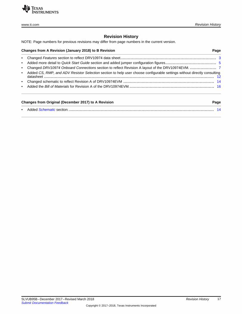
Revision HistoryNOTE: Page numbers for previous revisions may differ from page numbers in the current version.
Changes from A Revision (January 2018) to B Revision ............................................................................................... Page
• Changed Features section to reflect DRV10974 data sheet......................................................................... 3• Added more detail to Quick Start Guide section and added jumper configuration figures....................................... 5• Changed DRV10974 Onboard Connections section to reflect Revision A layout of the DRV10974EVM. .................... 7• Added CS, RMP, and ADV Resistor Selection section to help user choose configurable settings without directly consulting
datasheet ................................................................................................................................. 12• Changed schematic to reflect Revision A of DRV10974EVM ..................................................................... 14• Added the Bill of Materials for Revision A of the DRV10974EVM................................................................. 16
Changes from Original (December 2017) to A Revision ................................................................................................ Page
• Added Schematic section. .............................................................................................................. 14

IMPORTANT NOTICE FOR TI DESIGN INFORMATION AND RESOURCES
Texas Instruments Incorporated (‘TI”) technical, application or other design advice, services or information, including, but not limited to,reference designs and materials relating to evaluation modules, (collectively, “TI Resources”) are intended to assist designers who aredeveloping applications that incorporate TI products; by downloading, accessing or using any particular TI Resource in any way, you(individually or, if you are acting on behalf of a company, your company) agree to use it solely for this purpose and subject to the terms ofthis Notice.TI’s provision of TI Resources does not expand or otherwise alter TI’s applicable published warranties or warranty disclaimers for TIproducts, and no additional obligations or liabilities arise from TI providing such TI Resources. TI reserves the right to make corrections,enhancements, improvements and other changes to its TI Resources.You understand and agree that you remain responsible for using your independent analysis, evaluation and judgment in designing yourapplications and that you have full and exclusive responsibility to assure the safety of your applications and compliance of your applications(and of all TI products used in or for your applications) with all applicable regulations, laws and other applicable requirements. Yourepresent that, with respect to your applications, you have all the necessary expertise to create and implement safeguards that (1)anticipate dangerous consequences of failures, (2) monitor failures and their consequences, and (3) lessen the likelihood of failures thatmight cause harm and take appropriate actions. You agree that prior to using or distributing any applications that include TI products, youwill thoroughly test such applications and the functionality of such TI products as used in such applications. TI has not conducted anytesting other than that specifically described in the published documentation for a particular TI Resource.You are authorized to use, copy and modify any individual TI Resource only in connection with the development of applications that includethe TI product(s) identified in such TI Resource. NO OTHER LICENSE, EXPRESS OR IMPLIED, BY ESTOPPEL OR OTHERWISE TOANY OTHER TI INTELLECTUAL PROPERTY RIGHT, AND NO LICENSE TO ANY TECHNOLOGY OR INTELLECTUAL PROPERTYRIGHT OF TI OR ANY THIRD PARTY IS GRANTED HEREIN, including but not limited to any patent right, copyright, mask work right, orother intellectual property right relating to any combination, machine, or process in which TI products or services are used. Informationregarding or referencing third-party products or services does not constitute a license to use such products or services, or a warranty orendorsement thereof. Use of TI Resources may require a license from a third party under the patents or other intellectual property of thethird party, or a license from TI under the patents or other intellectual property of TI.TI RESOURCES ARE PROVIDED “AS IS” AND WITH ALL FAULTS. TI DISCLAIMS ALL OTHER WARRANTIES ORREPRESENTATIONS, EXPRESS OR IMPLIED, REGARDING TI RESOURCES OR USE THEREOF, INCLUDING BUT NOT LIMITED TOACCURACY OR COMPLETENESS, TITLE, ANY EPIDEMIC FAILURE WARRANTY AND ANY IMPLIED WARRANTIES OFMERCHANTABILITY, FITNESS FOR A PARTICULAR PURPOSE, AND NON-INFRINGEMENT OF ANY THIRD PARTY INTELLECTUALPROPERTY RIGHTS.TI SHALL NOT BE LIABLE FOR AND SHALL NOT DEFEND OR INDEMNIFY YOU AGAINST ANY CLAIM, INCLUDING BUT NOTLIMITED TO ANY INFRINGEMENT CLAIM THAT RELATES TO OR IS BASED ON ANY COMBINATION OF PRODUCTS EVEN IFDESCRIBED IN TI RESOURCES OR OTHERWISE. IN NO EVENT SHALL TI BE LIABLE FOR ANY ACTUAL, DIRECT, SPECIAL,COLLATERAL, INDIRECT, PUNITIVE, INCIDENTAL, CONSEQUENTIAL OR EXEMPLARY DAMAGES IN CONNECTION WITH ORARISING OUT OF TI RESOURCES OR USE THEREOF, AND REGARDLESS OF WHETHER TI HAS BEEN ADVISED OF THEPOSSIBILITY OF SUCH DAMAGES.You agree to fully indemnify TI and its representatives against any damages, costs, losses, and/or liabilities arising out of your non-compliance with the terms and provisions of this Notice.This Notice applies to TI Resources. Additional terms apply to the use and purchase of certain types of materials, TI products and services.These include; without limitation, TI’s standard terms for semiconductor products http://www.ti.com/sc/docs/stdterms.htm), evaluationmodules, and samples (http://www.ti.com/sc/docs/sampterms.htm).
Mailing Address: Texas Instruments, Post Office Box 655303, Dallas, Texas 75265Copyright © 2018, Texas Instruments Incorporated