Embed Size (px)
Citation preview
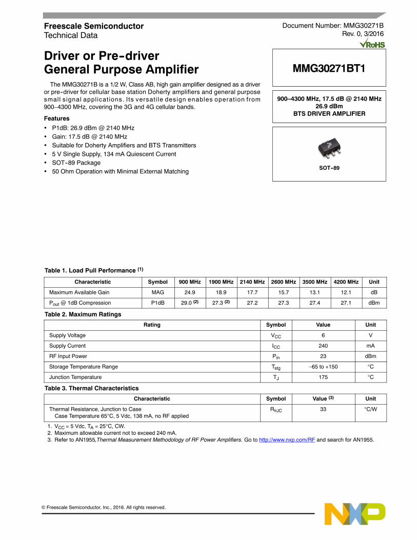
MMG30271BT1
1RF Device DataFreescale Semiconductor, Inc.
Driver or Pre--driverGeneral Purpose AmplifierThe MMG30271B is a 1/2 W, Class AB, high gain amplifier designed as a driver
or pre--driver for cellular base station Doherty amplifiers and general purposesmall s ignal appl icat ions. Its versati le design enables operation from900–4300 MHz, covering the 3G and 4G cellular bands.
Features
P1dB: 26.9 dBm @ 2140 MHz Gain: 17.5 dB @ 2140 MHz Suitable for Doherty Amplifiers and BTS Transmitters 5 V Single Supply, 134 mA Quiescent Current SOT--89 Package 50 Ohm Operation with Minimal External Matching
Table 1. Load Pull Performance (1)
Characteristic Symbol 900 MHz 1900 MHz 2140 MHz 2600 MHz 3500 MHz 4200 MHz Unit
Maximum Available Gain MAG 24.9 18.9 17.7 15.7 13.1 12.1 dB
Pout @ 1dB Compression P1dB 29.0 (2) 27.3 (2) 27.2 27.3 27.4 27.1 dBm
Table 2. Maximum Ratings
Rating Symbol Value Unit
Supply Voltage VCC 6 V
Supply Current ICC 240 mA
RF Input Power Pin 23 dBm
Storage Temperature Range Tstg –65 to +150 C
Junction Temperature TJ 175 C
Table 3. Thermal Characteristics
Characteristic Symbol Value (3) Unit
Thermal Resistance, Junction to CaseCase Temperature 65C, 5 Vdc, 138 mA, no RF applied
RJC 33 C/W
1. VCC = 5 Vdc, TA = 25C, CW.2. Maximum allowable current not to exceed 240 mA.3. Refer to AN1955,Thermal Measurement Methodology of RF Power Amplifiers. Go to http://www.nxp.com/RF and search for AN1955.
Document Number: MMG30271BRev. 0, 3/2016
Freescale SemiconductorTechnical Data
MMG30271BT1
SOT--89
900–4300 MHz, 17.5 dB @ 2140 MHz26.9 dBm
BTS DRIVER AMPLIFIER
Freescale Semiconductor, Inc., 2016. All rights reserved.
2RF Device Data
Freescale Semiconductor, Inc.
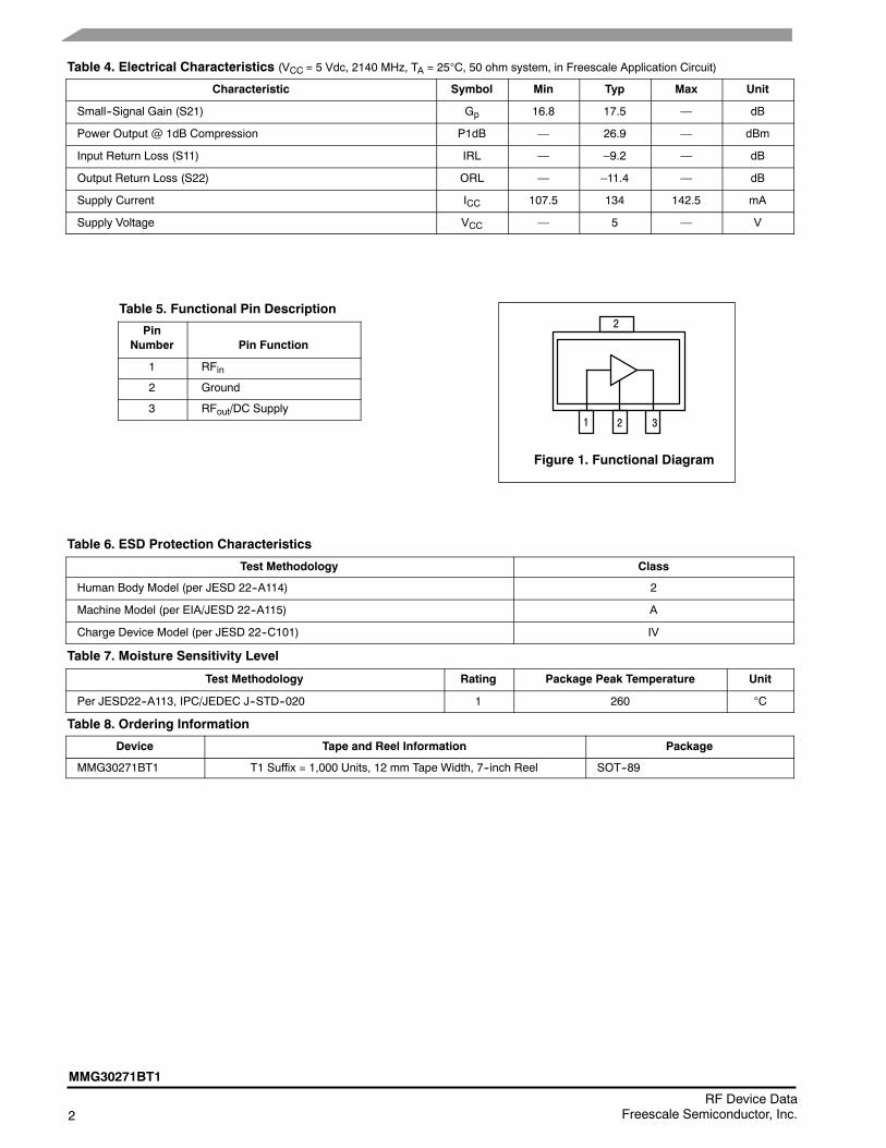
MMG30271BT1
Table 4. Electrical Characteristics (VCC = 5 Vdc, 2140 MHz, TA = 25C, 50 ohm system, in Freescale Application Circuit)
Characteristic Symbol Min Typ Max Unit
Small--Signal Gain (S21) Gp 16.8 17.5 — dB
Power Output @ 1dB Compression P1dB — 26.9 — dBm
Input Return Loss (S11) IRL — –9.2 — dB
Output Return Loss (S22) ORL — –11.4 — dB
Supply Current ICC 107.5 134 142.5 mA
Supply Voltage VCC — 5 — V
Table 5. Functional Pin Description
PinNumber Pin Function
1 RFin
2 Ground
3 RFout/DC Supply
Table 6. ESD Protection Characteristics
Test Methodology Class
Human Body Model (per JESD 22--A114) 2
Machine Model (per EIA/JESD 22--A115) A
Charge Device Model (per JESD 22--C101) IV
Table 7. Moisture Sensitivity Level
Test Methodology Rating Package Peak Temperature Unit
Per JESD22--A113, IPC/JEDEC J--STD--020 1 260 C
Table 8. Ordering Information
Device Tape and Reel Information Package
MMG30271BT1 T1 Suffix = 1,000 Units, 12 mm Tape Width, 7--inch Reel SOT--89
Figure 1. Functional Diagram
321
2
MMG30271BT1
3RF Device DataFreescale Semiconductor, Inc.
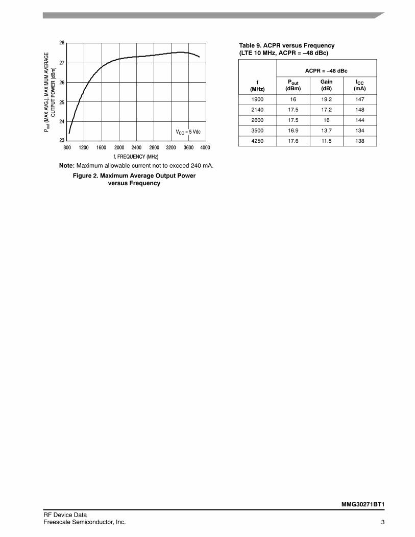
Table 9. ACPR versus Frequency(LTE 10 MHz, ACPR = –48 dBc)
f(MHz)
ACPR = –48 dBc
Pout(dBm)
Gain(dB)
ICC(mA)
1900 16 19.2 147
2140 17.5 17.2 148
2600 17.5 16 144
3500 16.9 13.7 134
4250 17.6 11.5 13823800 1200 1600 2000 4000
25
24
26
27
28
2400
f, FREQUENCY (MHz)
Figure 2. Maximum Average Output Powerversus Frequency
P out(MAX
AVG.),MAXIMUMAVERAGE
OUTPUTPOWER
(dBm
)
2800 3200 3600
VCC = 5 Vdc
Note: Maximum allowable current not to exceed 240 mA.
4RF Device Data
Freescale Semiconductor, Inc.
MMG30271BT1
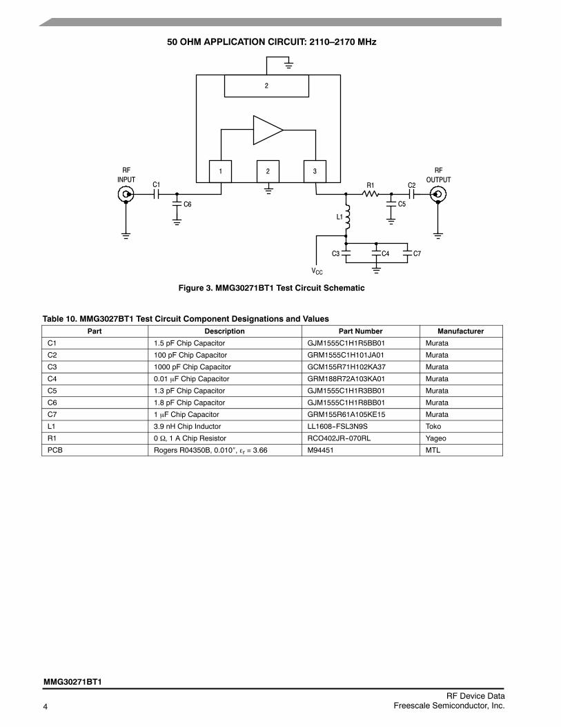
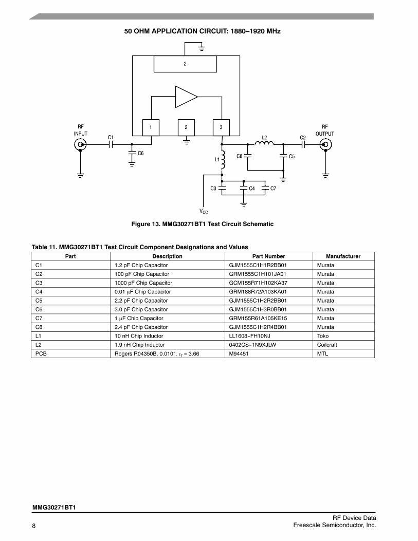
50 OHM APPLICATION CIRCUIT: 2110–2170 MHz
Figure 3. MMG30271BT1 Test Circuit Schematic
RFOUTPUT
RFINPUT
C1
C6
1 2 3
2
L1
C5
C4 C7
C2
VCC
C3
R1
Table 10. MMG3027BT1 Test Circuit Component Designations and ValuesPart Description Part Number Manufacturer
C1 1.5 pF Chip Capacitor GJM1555C1H1R5BB01 Murata
C2 100 pF Chip Capacitor GRM1555C1H101JA01 Murata
C3 1000 pF Chip Capacitor GCM155R71H102KA37 Murata
C4 0.01 F Chip Capacitor GRM188R72A103KA01 Murata
C5 1.3 pF Chip Capacitor GJM1555C1H1R3BB01 Murata
C6 1.8 pF Chip Capacitor GJM1555C1H1R8BB01 Murata
C7 1 F Chip Capacitor GRM155R61A105KE15 Murata
L1 3.9 nH Chip Inductor LL1608--FSL3N9S Toko
R1 0 , 1 A Chip Resistor RCO402JR--070RL Yageo
PCB Rogers R04350B, 0.010, r = 3.66 M94451 MTL
MMG30271BT1
5RF Device DataFreescale Semiconductor, Inc.
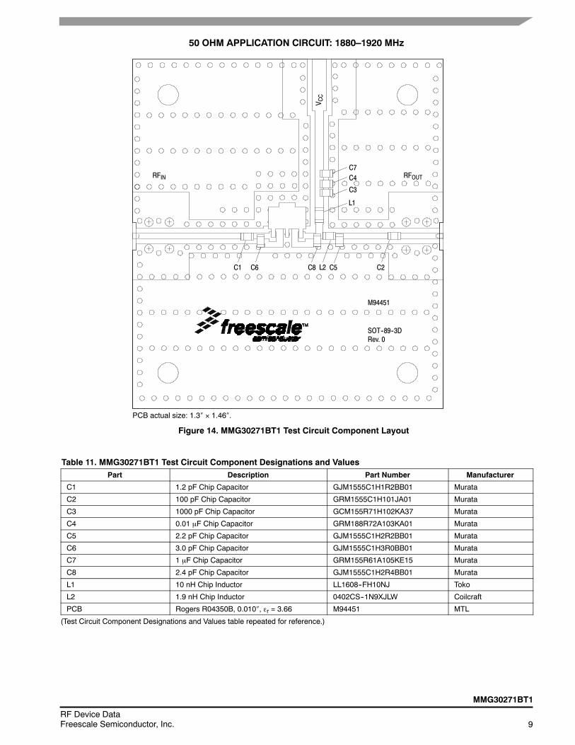
50 OHM APPLICATION CIRCUIT: 2110–2170 MHz
Figure 4. MMG30271BT1 Test Circuit Component Layout
PCB actual size: 1.3 1.46.
C7C4
C3
L1
C5
C2
R1C6
C1
RFINRFOUT
SOT--89--3DRev. 0
V CC
M94451
Table 10. MMG30371BT1 Test Circuit Component Designations and ValuesPart Description Part Number Manufacturer
C1 1.5 pF Chip Capacitor GJM1555C1H1R5BB01 Murata
C2 100 pF Chip Capacitor GRM1555C1H101JA01 Murata
C3 1000 pF Chip Capacitor GCM155R71H102KA37 Murata
C4 0.01 F Chip Capacitor GRM188R72A103KA01 Murata
C5 1.3 pF Chip Capacitor GJM1555C1H1R3BB01 Murata
C6 1.8 pF Chip Capacitor GJM1555C1H1R8BB01 Murata
C7 1 F Chip Capacitor GRM155R61A105KE15 Murata
L1 3.9 nH Chip Inductor LL1608--FSL3N9S Toko
R1 0 , 1 A Chip Resistor RCO402JR--070RL Yageo
PCB Rogers R04350B, 0.010, r = 3.66 M94451 MTL
(Test Circuit Component Designations and Values table repeated for reference.)
6RF Device Data
Freescale Semiconductor, Inc.
MMG30271BT1
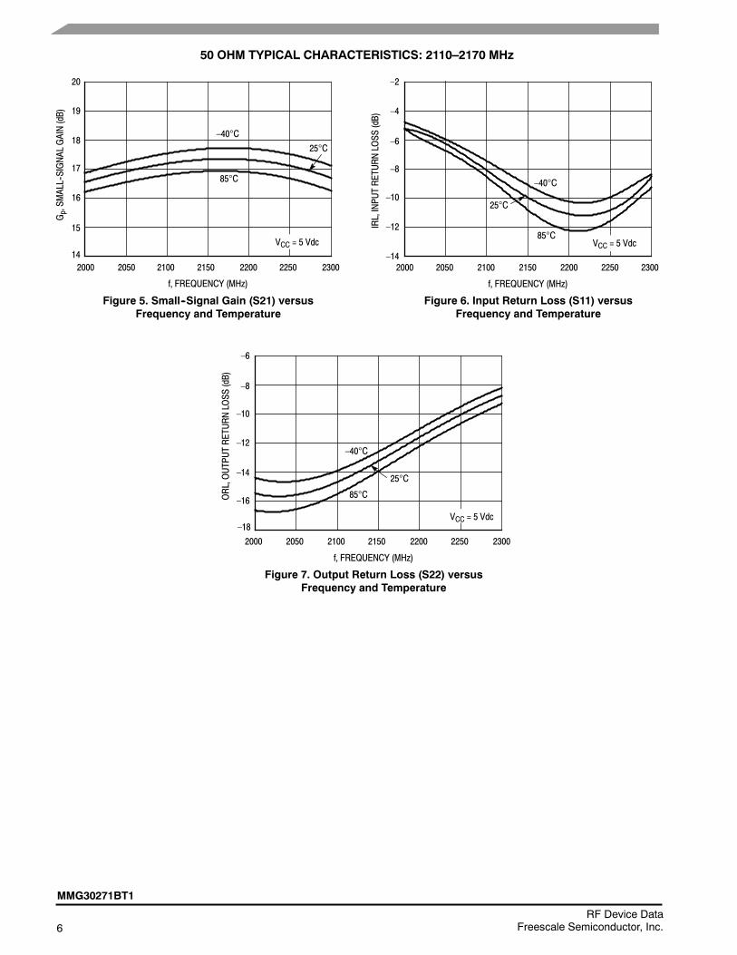
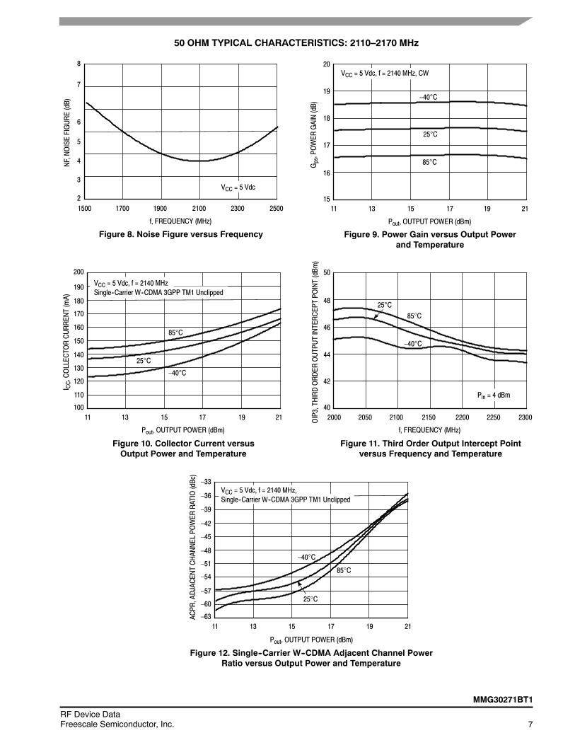
50 OHM TYPICAL CHARACTERISTICS: 2110–2170 MHz
14
20
2000
f, FREQUENCY (MHz)
Figure 5. Small--Signal Gain (S21) versusFrequency and Temperature
VCC = 5 Vdc
17
Gp,SM
ALL--SIGNAL
GAIN(dB) 19
16
2050 2150 2250 2300
–40C
85C
25C
22002100
15
18
–12
–2
f, FREQUENCY (MHz)
Figure 6. Input Return Loss (S11) versusFrequency and Temperature
IRL,INPUTRETURNLOSS
(dB)
–6
2000 2050 2100 2200 2300
–4
–8
85C
25C–10
–142150 2250
VCC = 5 Vdc
–40C
–18
–6
ORL,OUTPUTRETURNLOSS
(dB)
–14
VCC = 5 Vdc
2000 2050 2100 2150 2200
–12
–16
25C
85C
2250 2300
–10
–8
–40C
f, FREQUENCY (MHz)
Figure 7. Output Return Loss (S22) versusFrequency and Temperature
MMG30271BT1
7RF Device DataFreescale Semiconductor, Inc.
50 OHM TYPICAL CHARACTERISTICS: 2110–2170 MHz
8
f, FREQUENCY (MHz)
Figure 8. Noise Figure versus Frequency
NF,NOISEFIGURE(dB)
1500 1700 1900 2100 2300
7
4
2
6
5
3
250015
19
17
16
Pout, OUTPUT POWER (dBm)
Figure 9. Power Gain versus Output Powerand Temperature
Gps,POWER
GAIN(dB)
18
VCC = 5 Vdc, f = 2140 MHz, CW
–40C
85C
11 13 15 17 21
25C
19
20
100
150
130
11 13 15 17 21
140
120
Pout, OUTPUT POWER (dBm)
Figure 10. Collector Current versusOutput Power and Temperature
I CC,COLLECTORCURRENT(mA)
85C
25C
–40C
VCC = 5 Vdc, f = 2140 MHzSingle--Carrier W--CDMA 3GPP TM1 Unclipped
110
160
170
180
190
200
1940
50
44
2000 2050 2100 2200 2300
46
42
f, FREQUENCY (MHz)
Figure 11. Third Order Output Intercept Pointversus Frequency and Temperature
OIP3,THIRDORDER
OUTPUTINTERCEPTPOINT(dBm
)
Pin = 4 dBm
25C
–40C
85C
2150 2250
48
VCC = 5 Vdc
–63
–33
11
Pout, OUTPUT POWER (dBm)
Figure 12. Single--Carrier W--CDMA Adjacent Channel PowerRatio versus Output Power and Temperature
–39
–42
–54
21191513
ACPR,ADJACENTCHANNEL
POWER
RATIO(dBc)
85C
VCC = 5 Vdc, f = 2140 MHz,Single--Carrier W--CDMA 3GPP TM1 Unclipped
17
–40C
25C
–36
–45
–48
–51
–57
–60
8RF Device Data
Freescale Semiconductor, Inc.
MMG30271BT1
50 OHM APPLICATION CIRCUIT: 1880–1920 MHz
Figure 13. MMG30271BT1 Test Circuit Schematic
RFOUTPUT
RFINPUT
C1
1 2 3
2
L1
C3
C2
VCC
C6
C7C4
C5
L2
C8
Table 11. MMG30271BT1 Test Circuit Component Designations and ValuesPart Description Part Number Manufacturer
C1 1.2 pF Chip Capacitor GJM1555C1H1R2BB01 Murata
C2 100 pF Chip Capacitor GRM1555C1H101JA01 Murata
C3 1000 pF Chip Capacitor GCM155R71H102KA37 Murata
C4 0.01 F Chip Capacitor GRM188R72A103KA01 Murata
C5 2.2 pF Chip Capacitor GJM1555C1H2R2BB01 Murata
C6 3.0 pF Chip Capacitor GJM1555C1H3R0BB01 Murata
C7 1 F Chip Capacitor GRM155R61A105KE15 Murata
C8 2.4 pF Chip Capacitor GJM1555C1H2R4BB01 Murata
L1 10 nH Chip Inductor LL1608--FH10NJ Toko
L2 1.9 nH Chip Inductor 0402CS--1N9XJLW Coilcraft
PCB Rogers R04350B, 0.010, r = 3.66 M94451 MTL
MMG30271BT1
9RF Device DataFreescale Semiconductor, Inc.
50 OHM APPLICATION CIRCUIT: 1880–1920 MHz
Figure 14. MMG30271BT1 Test Circuit Component Layout
PCB actual size: 1.3 1.46.
C7C4
C3
L1
C1 C6 C8 L2 C5 C2
V CC
SOT--89--3DRev. 0
RFIN RFOUT
M94451
Table 11. MMG30271BT1 Test Circuit Component Designations and ValuesPart Description Part Number Manufacturer
C1 1.2 pF Chip Capacitor GJM1555C1H1R2BB01 Murata
C2 100 pF Chip Capacitor GRM1555C1H101JA01 Murata
C3 1000 pF Chip Capacitor GCM155R71H102KA37 Murata
C4 0.01 F Chip Capacitor GRM188R72A103KA01 Murata
C5 2.2 pF Chip Capacitor GJM1555C1H2R2BB01 Murata
C6 3.0 pF Chip Capacitor GJM1555C1H3R0BB01 Murata
C7 1 F Chip Capacitor GRM155R61A105KE15 Murata
C8 2.4 pF Chip Capacitor GJM1555C1H2R4BB01 Murata
L1 10 nH Chip Inductor LL1608--FH10NJ Toko
L2 1.9 nH Chip Inductor 0402CS--1N9XJLW Coilcraft
PCB Rogers R04350B, 0.010, r = 3.66 M94451 MTL
(Test Circuit Component Designations and Values table repeated for reference.)
10RF Device Data
Freescale Semiconductor, Inc.
MMG30271BT1
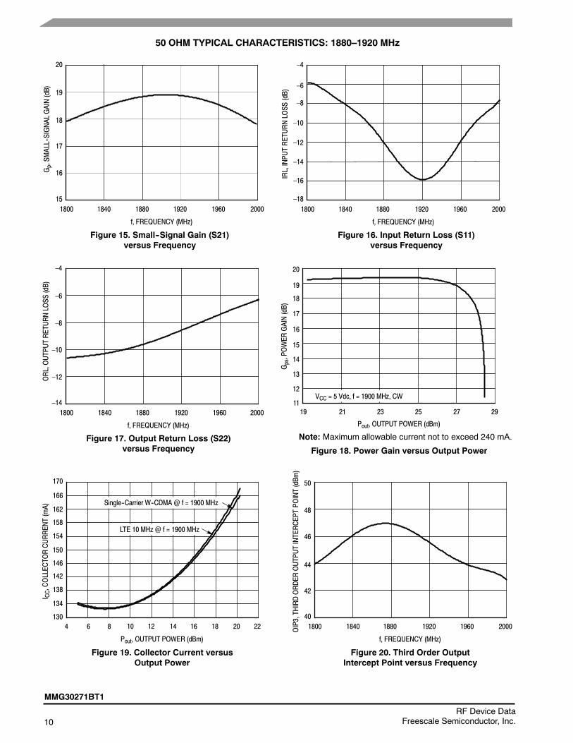
50 OHM TYPICAL CHARACTERISTICS: 1880–1920 MHz
15
20
1800
f, FREQUENCY (MHz)
Figure 15. Small--Signal Gain (S21)versus Frequency
18
Gp,SM
ALL--SIGNAL
GAIN(dB) 19
17
1840 1880 1920 1960
16
2000
–4
f, FREQUENCY (MHz)
Figure 16. Input Return Loss (S11)versus Frequency
IRL,INPUTRETURNLOSS
(dB)
–8
1800 1840 1880 1920 1960
–6
–14
–18
–10
–12
–16
2000
–14
–4
–10
1800 1840 1880 1920 2000
–8
–12ORL,OUTPUTRETURNLOSS
(dB)
f, FREQUENCY (MHz)
Figure 17. Output Return Loss (S22)versus Frequency
–6
196011
15
13
12
Pout, OUTPUT POWER (dBm)
Figure 18. Power Gain versus Output Power
Gps,POWER
GAIN(dB)
14
19
16
17
21 23 25 27 29
18
19
20
150
158
154
162
166
170
LTE 10 MHz @ f = 1900 MHz
Single--Carrier W--CDMA @ f = 1900 MHz
146
134
142
138
1306 8 10 12 2214
Pout, OUTPUT POWER (dBm)
Figure 19. Collector Current versusOutput Power
I CC,COLLECTORCURRENT(mA)
16 18 20440
48
44
1800 1840 1880 1920 2000
46
42
f, FREQUENCY (MHz)
Figure 20. Third Order OutputIntercept Point versus Frequency
OIP3,THIRDORDER
OUTPUTINTERCEPTPOINT(dBm
)
1960
50
VCC = 5 Vdc, f = 1900 MHz, CW
Note: Maximum allowable current not to exceed 240 mA.
MMG30271BT1
11RF Device DataFreescale Semiconductor, Inc.
50 OHM TYPICAL CHARACTERISTICS: 1880–1920 MHz
–62
–38
4
Pout, OUTPUT POWER (dBm)
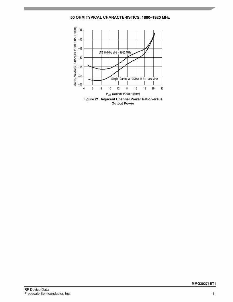
Figure 21. Adjacent Channel Power Ratio versusOutput Power
–42
–46
–54
1286
ACPR,ADJACENTCHANNEL
POWER
RATIO(dBc)
10
–50
–58
14 16 18 20
LTE 10 MHz @ f = 1900 MHz
Single--Carrier W--CDMA @ f = 1900 MHz
22
12RF Device Data
Freescale Semiconductor, Inc.
MMG30271BT1
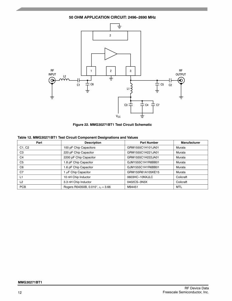
50 OHM APPLICATION CIRCUIT: 2496–2690 MHz
Figure 22. MMG30271BT1 Test Circuit Schematic
RFOUTPUT
RFINPUT
1 2 3
2
L1
C6 C2
L2
C1
C3
C5
VCC
C4 C7
Table 12. MMG30271BT1 Test Circuit Component Designations and ValuesPart Description Part Number Manufacturer
C1, C2 100 pF Chip Capacitors GRM1555C1H101JA01 Murata
C3 220 pF Chip Capacitor GRM1555C1H221JA01 Murata
C4 2200 pF Chip Capacitor GRM1555C1H222JA01 Murata
C5 1.8 pF Chip Capacitor GJM1555C1H1R8BB01 Murata
C6 1.6 pF Chip Capacitor GJM1555C1H1R6BB01 Murata
C7 1 F Chip Capacitor GRM155R61A105KE15 Murata
L1 10 nH Chip Inductor 0603HC--10NXJLC Coilcraft
L2 3.3 nH Chip Inductor 0402CS--3N3X Coilcraft
PCB Rogers R04350B, 0.010, r = 3.66 M94451 MTL
MMG30271BT1
13RF Device DataFreescale Semiconductor, Inc.
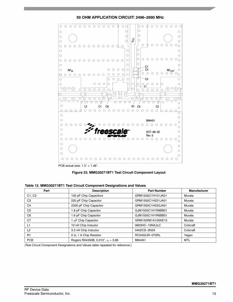
50 OHM APPLICATION CIRCUIT: 2496–2690 MHz
Figure 23. MMG30271BT1 Test Circuit Component Layout
PCB actual size: 1.3 1.46.
V CC
C4
C3
C2C5R1C6C1L2
L1
RFOUTRFINC7
SOT--89--3DRev. 0
M94451
Table 12. MMG30271BT1 Test Circuit Component Designations and ValuesPart Description Part Number Manufacturer
C1, C2 100 pF Chip Capacitors GRM1555C1H101JA01 Murata
C3 220 pF Chip Capacitor GRM1555C1H221JA01 Murata
C4 2200 pF Chip Capacitor GRM1555C1H222JA01 Murata
C5 1.8 pF Chip Capacitor GJM1555C1H1R8BB01 Murata
C6 1.6 pF Chip Capacitor GJM1555C1H1R6BB01 Murata
C7 1 F Chip Capacitor GRM155R61A105KE15 Murata
L1 10 nH Chip Inductor 0603HC--10NXJLC Coilcraft
L2 3.3 nH Chip Inductor 0402CS--3N3X Coilcraft
R1 0 , 1 A Chip Resistor RC0402JR--070RL Yageo
PCB Rogers R04350B, 0.010, r = 3.66 M94451 MTL
(Test Circuit Component Designations and Values table repeated for reference.)
14RF Device Data
Freescale Semiconductor, Inc.
MMG30271BT1
50 OHM TYPICAL CHARACTERISTICS: 2496–2690 MHzORL,OUTPUTRETURNLOSS
(dB)
VCC = 5 Vdc
12
18
2400
f, FREQUENCY (MHz)
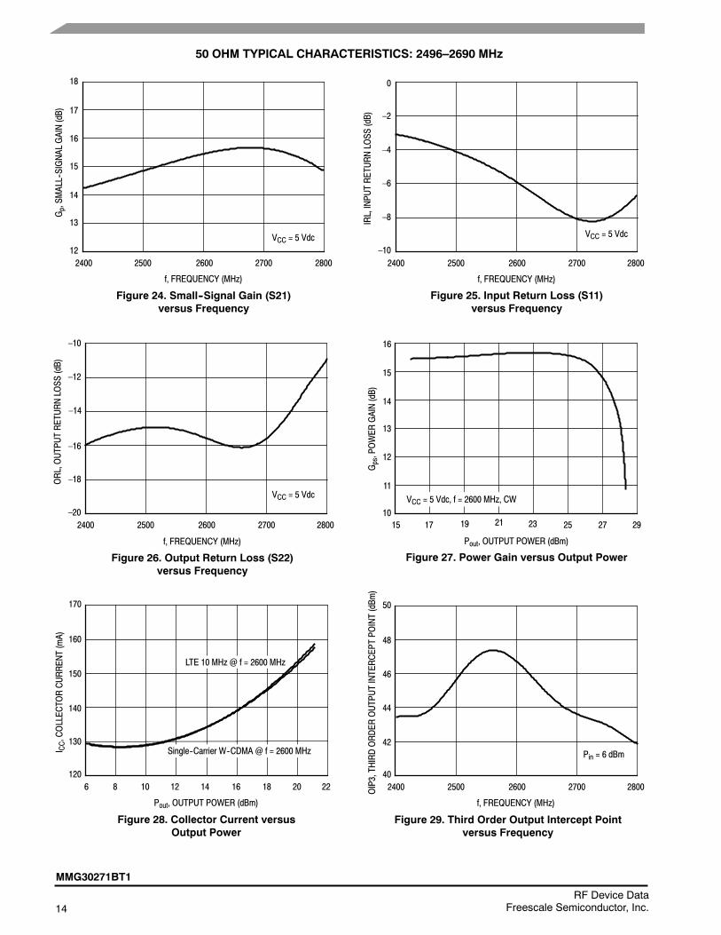
Figure 24. Small--Signal Gain (S21)versus Frequency
VCC = 5 Vdc
14
Gp,SM
ALL--SIGNAL
GAIN(dB)
15
13
2500 2600 2700 2800
16
17–2
f, FREQUENCY (MHz)
Figure 25. Input Return Loss (S11)versus Frequency
IRL,INPUTRETURNLOSS
(dB)
–6
VCC = 5 Vdc
2400 2500 2600 2700 2800
–4
–8
–10
0
–20
–10
2400 2500 2600 2700 2800
–12
–14
–16
–18
f, FREQUENCY (MHz)
Figure 26. Output Return Loss (S22)versus Frequency
10
14
12
11
Pout, OUTPUT POWER (dBm)
Figure 27. Power Gain versus Output Power
Gps,POWER
GAIN(dB)
13
VCC = 5 Vdc, f = 2600 MHz, CW
15 17 19 21 2523
15
27 29
16
1206 8 10 12 22
140
130
150
160
170
14
Pout, OUTPUT POWER (dBm)
Figure 28. Collector Current versusOutput Power
I CC,COLLECTORCURRENT(mA)
16 18 20
LTE 10 MHz @ f = 2600 MHz
Single--Carrier W--CDMA @ f = 2600 MHz
40
50
46
2400 2500 2600 2700 2800
48
44
Pin = 6 dBm
f, FREQUENCY (MHz)
Figure 29. Third Order Output Intercept Pointversus Frequency
OIP3,THIRDORDER
OUTPUTINTERCEPTPOINT(dBm
)
42
MMG30271BT1
15RF Device DataFreescale Semiconductor, Inc.
50 OHM TYPICAL CHARACTERISTICS: 2496–2690 MHz
–60
–36
4
Pout, OUTPUT POWER (dBm)
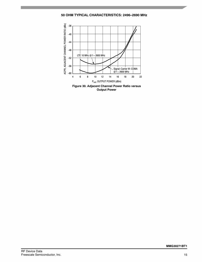
Figure 30. Adjacent Channel Power Ratio versusOutput Power
–40
–44
–52
221286
ACPR,ADJACENTCHANNEL
POWER
RATIO(dBc)
10
–48
–56
14 16 18 20
LTE 10 MHz @ f = 2600 MHz
Signal--Carrier W--CDMA@ f = 2600 MHz
16RF Device Data
Freescale Semiconductor, Inc.
MMG30271BT1
50 OHM APPLICATION CIRCUIT: 3400–3600 MHz
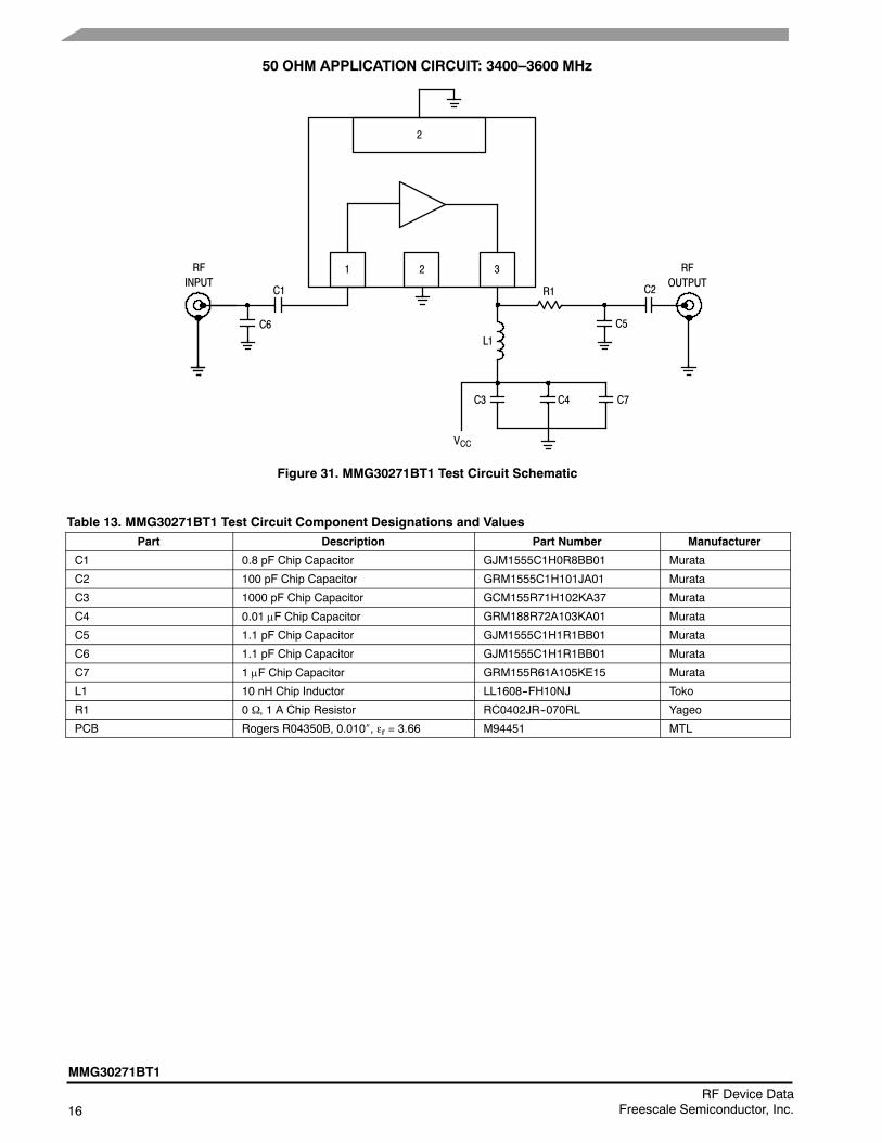
Figure 31. MMG30271BT1 Test Circuit Schematic
RFOUTPUT
RFINPUT
1 2 3
2
L1
C4 C7
C2
VCC
C6
C1
C5
C3
R1
Table 13. MMG30271BT1 Test Circuit Component Designations and ValuesPart Description Part Number Manufacturer
C1 0.8 pF Chip Capacitor GJM1555C1H0R8BB01 Murata
C2 100 pF Chip Capacitor GRM1555C1H101JA01 Murata
C3 1000 pF Chip Capacitor GCM155R71H102KA37 Murata
C4 0.01 F Chip Capacitor GRM188R72A103KA01 Murata
C5 1.1 pF Chip Capacitor GJM1555C1H1R1BB01 Murata
C6 1.1 pF Chip Capacitor GJM1555C1H1R1BB01 Murata
C7 1 F Chip Capacitor GRM155R61A105KE15 Murata
L1 10 nH Chip Inductor LL1608--FH10NJ Toko
R1 0 , 1 A Chip Resistor RC0402JR--070RL Yageo
PCB Rogers R04350B, 0.010, r = 3.66 M94451 MTL
MMG30271BT1
17RF Device DataFreescale Semiconductor, Inc.
50 OHM APPLICATION CIRCUIT: 3400–3600 MHz
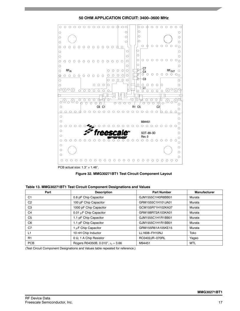
Figure 32. MMG30271BT1 Test Circuit Component Layout
PCB actual size: 1.3 1.46.
C3
SOT--89--3DRev. 0
RFINC7C4
L1
C6 C1 R1 C5 C2
RFOUT
M94451
Table 13. MMG30271BT1 Test Circuit Component Designations and ValuesPart Description Part Number Manufacturer
C1 0.8 pF Chip Capacitor GJM1555C1H0R8BB01 Murata
C2 100 pF Chip Capacitor GRM1555C1H101JA01 Murata
C3 1000 pF Chip Capacitor GCM155R71H102KA37 Murata
C4 0.01 F Chip Capacitor GRM188R72A103KA01 Murata
C5 1.1 pF Chip Capacitor GJM1555C1H1R1BB01 Murata
C6 1.1 pF Chip Capacitor GJM1555C1H1R1BB01 Murata
C7 1 F Chip Capacitor GRM155R61A105KE15 Murata
L1 10 nH Chip Inductor LL1608--FH10NJ Toko
R1 0 , 1 A Chip Resistor RC0402JR--070RL Yageo
PCB Rogers R04350B, 0.010, r = 3.66 M94451 MTL
(Test Circuit Component Designations and Values table repeated for reference.)
18RF Device Data
Freescale Semiconductor, Inc.
MMG30271BT1
50 OHM TYPICAL CHARACTERISTICS: 3400–3600 MHz
8
12
3200
f, FREQUENCY (MHz)
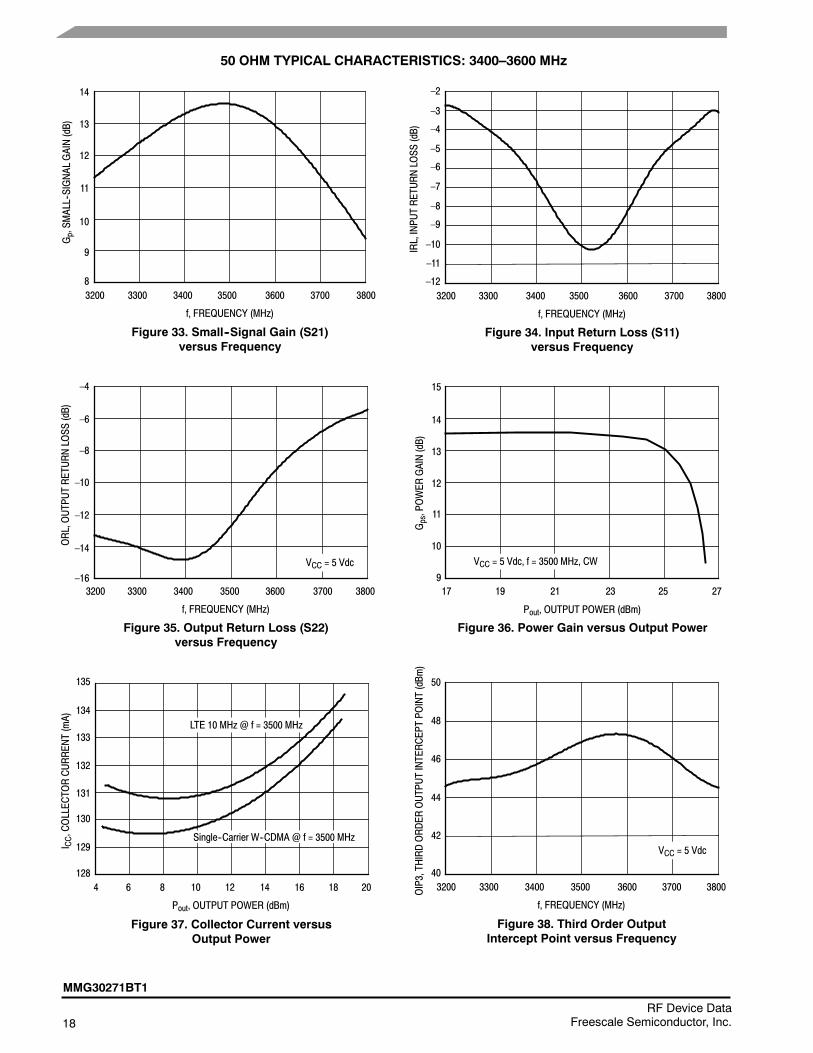
Figure 33. Small--Signal Gain (S21)versus Frequency
10
Gp,SM
ALL--SIGNAL
GAIN(dB)
11
9
3300 3400 3500 3600
13
14
3700 3800
–2
–7
3200 3400 3500 3600 3800
–5
–9
–12
–11
–10
–8
–6
–4
–3
3300 3700
f, FREQUENCY (MHz)
Figure 34. Input Return Loss (S11)versus Frequency
IRL,INPUTRETURNLOSS
(dB)
–12
–4
–8
3200 3300 3400 3500 3600
–6
–10
f, FREQUENCY (MHz)
Figure 35. Output Return Loss (S22)versus Frequency
ORL,OUTPUTRETURNLOSS
(dB)
VCC = 5 Vdc–14
–163700 3800
9
13
11
10
Pout, OUTPUT POWER (dBm)
Figure 36. Power Gain versus Output Power
Gps,POWER
GAIN(dB)
12
VCC = 5 Vdc, f = 3500 MHz, CW
17 19 21 23 2725
15
14
1284 6 8 10 20
132
131
133
134
135
12
Pout, OUTPUT POWER (dBm)
Figure 37. Collector Current versusOutput Power
I CC,COLLECTORCURRENT(mA)
14 16 18
LTE 10 MHz @ f = 3500 MHz
Single--Carrier W--CDMA @ f = 3500 MHz
130
12942
50
46
3200 3300 3400 3500 3600
48
44
VCC = 5 Vdc
f, FREQUENCY (MHz)
Figure 38. Third Order OutputIntercept Point versus Frequency
OIP3,THIRDORDER
OUTPUTINTERCEPTPOINT(dBm
)
403700 3800
MMG30271BT1
19RF Device DataFreescale Semiconductor, Inc.
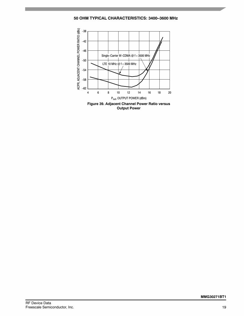
50 OHM TYPICAL CHARACTERISTICS: 3400–3600 MHz
–62
–38
4
Pout, OUTPUT POWER (dBm)
Figure 39. Adjacent Channel Power Ratio versusOutput Power
–42
–46
–54
1286
ACPR,ADJACENTCHANNEL
POWER
RATIO(dBc)
10
–50
–58
14 16 18 20
LTE 10 MHz @ f = 3500 MHz
Single--Carrier W--CDMA @ f = 3500 MHz
20RF Device Data
Freescale Semiconductor, Inc.
MMG30271BT1
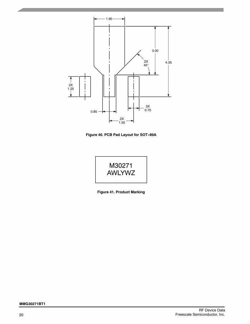
Figure 40. PCB Pad Layout for SOT--89A
4.35
3.00
2X45
3X0.70
2X1.50
0.85
2X1.25
1.90
M30271AWLYWZ
Figure 41. Product Marking
MMG30271BT1
21RF Device DataFreescale Semiconductor, Inc.
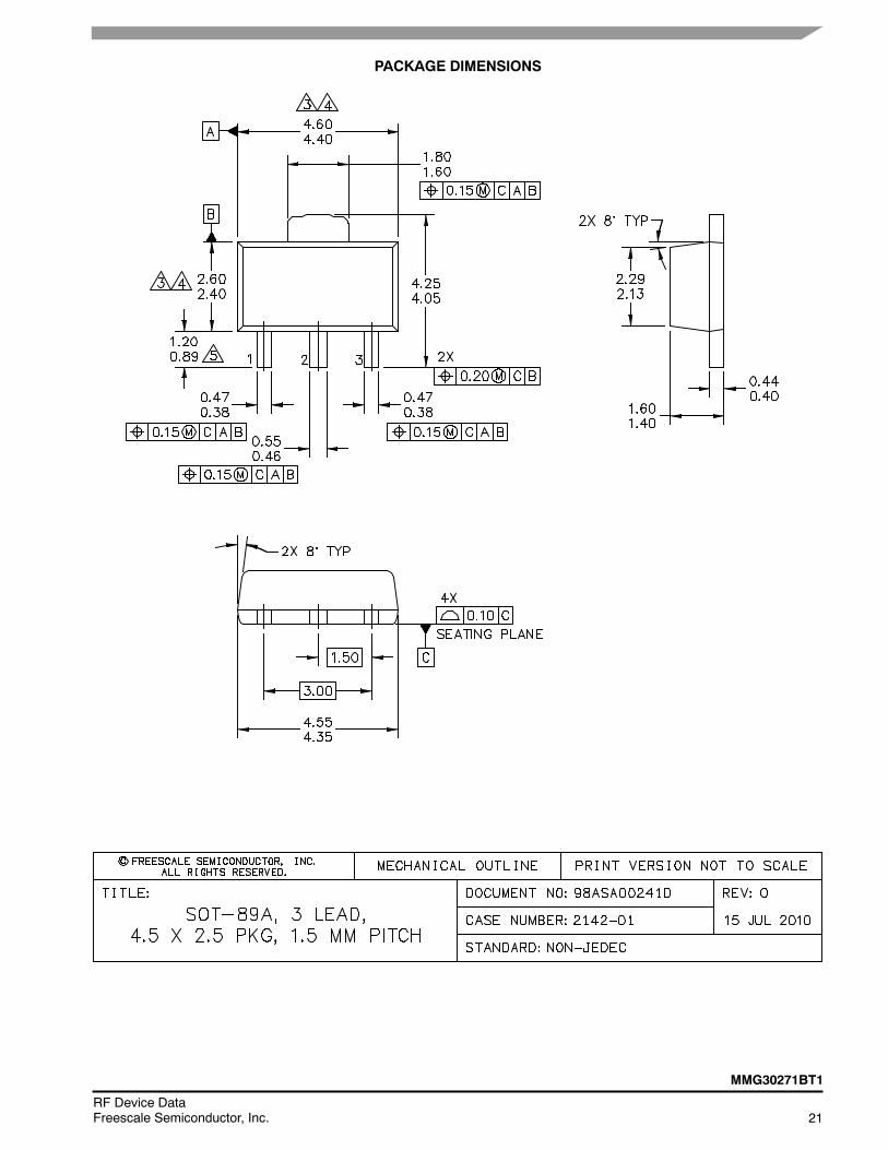
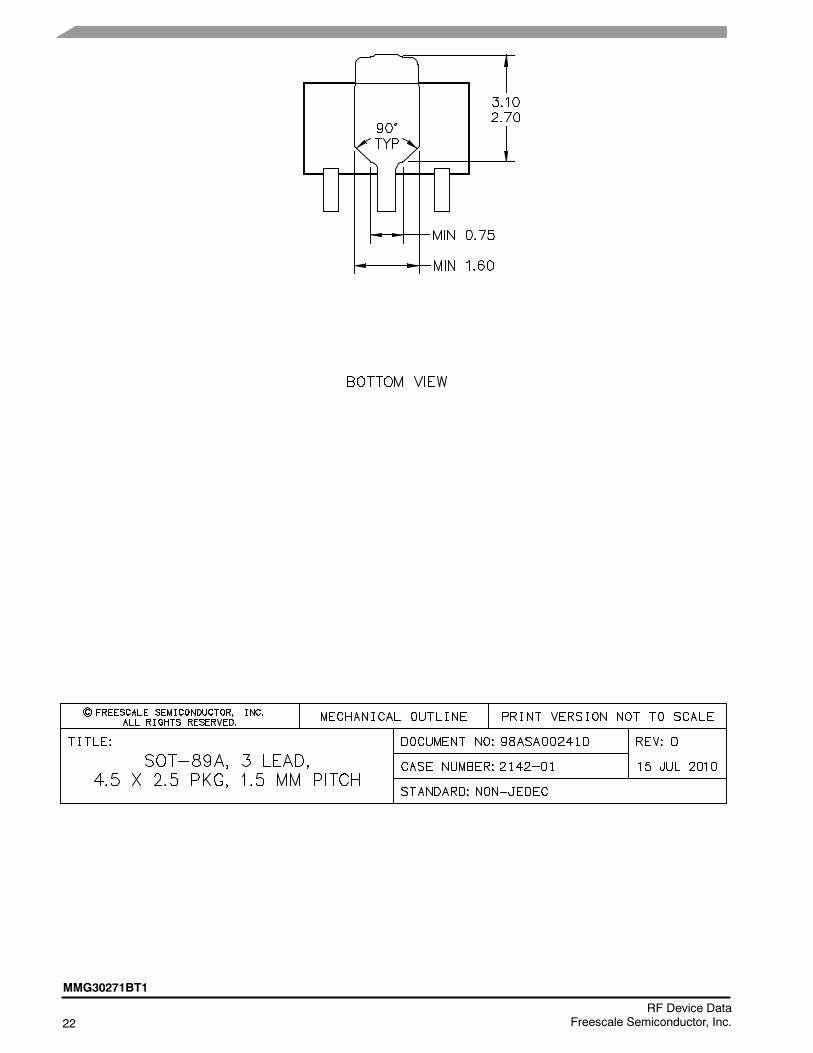
PACKAGE DIMENSIONS
22RF Device Data
Freescale Semiconductor, Inc.
MMG30271BT1
MMG30271BT1
23RF Device DataFreescale Semiconductor, Inc.
24RF Device Data
Freescale Semiconductor, Inc.
MMG30271BT1
PRODUCT DOCUMENTATION, SOFTWARE AND TOOLSRefer to the following resources to aid your design process.
Application Notes AN1955: Thermal Measurement Methodology of RF Power Amplifiers
Software .s2p File
Development Tools Printed Circuit Boards
To Download Resources Specific to a Given Part Number:2. Go to http://www.nxp.com/RF
3. Search by part number
4. Click part number link
5. Choose the desired resource from the drop down menu
FAILURE ANALYSIS
At this time, because of the physical characteristics of the part, failure analysis is limited to electrical signature analysis. Incases where Freescale is contractually obligated to perform failure analysis (FA) services, full FA may be performed by thirdparty vendors with moderate success. For updates contact your local Freescale Sales Office.
REVISION HISTORY
The following table summarizes revisions to this document.
Revision Date Description
0 Mar. 2016 Initial Release of Data Sheet
MMG30271BT1
25RF Device DataFreescale Semiconductor, Inc.
Information in this document is provided solely to enable system and softwareimplementers to use Freescale products. There are no express or implied copyrightlicenses granted hereunder to design or fabricate any integrated circuits based on theinformation in this document.
Freescale reserves the right to make changes without further notice to any productsherein. Freescale makes no warranty, representation, or guarantee regarding thesuitability of its products for any particular purpose, nor does Freescale assume anyliability arising out of the application or use of any product or circuit, and specificallydisclaims any and all liability, including without limitation consequential or incidentaldamages. “Typical” parameters that may be provided in Freescale data sheets and/orspecifications can and do vary in different applications, and actual performance mayvary over time. All operating parameters, including “typicals,” must be validated foreach customer application by customer’s technical experts. Freescale does not conveyany license under its patent rights nor the rights of others. Freescale sells productspursuant to standard terms and conditions of sale, which can be found at the followingaddress: freescale.com/SalesTermsandConditions.
Freescale and the Freescale logo are trademarks of Freescale Semiconductor, Inc.,Reg. U.S. Pat. & Tm. Off. All other product or service names are the property of theirrespective owners.E 2016 Freescale Semiconductor, Inc.
How to Reach Us:
Home Page:freescale.com
Web Support:freescale.com/support
Document Number: MMG30271BRev. 0, 3/2016