Embed Size (px)
Citation preview

Copyright © by John Wiley & Sons 2003 Drive Ckts - 1
Drive Circuits
Outline
• Drive circuit design considerations
• DC-coupled drive circuits
• Isolated drive circuits
• Protection measures in drive circuits
• Component/circuit layout considerations

Copyright © by John Wiley & Sons 2003 Drive Ckts - 2
Functionality of Gate/Base Drive Circuits• Turn power switch from off-state to on-state
• Minimize turn-on time through active region where power dissipation is large
• Provide adequate drive power to keep power switch in on-state
• Turn power switch from on-state to off-state
• Minimize turn-off time through active region wherepower dissipation is large
• Provide bias to insure that power switch remains off
• Control power switch to protect it when overvoltages or overcurrents are sensed
• Signal processing circuits which generate the logic control signals not considered part of the drive circuit
• Drive circuit amplifies control signals to levels required to drive power switch
• Drive circuit has significant power capabilities compared to logic level signal processing circuits
• Provide electrical isolation when needed between power switch and logic level signal processing/control circuits

Copyright © by John Wiley & Sons 2003 Drive Ckts - 3
• Drive circuit topologies
• Output signal polarity - unipolar or bipolar• AC or DC coupled• Connected in shunt or series with power switch
• Output current magnitude• Large Ion shortens turn-on time but lengthens turn-off delay time• Large Ioff shortens turn-off time but lengthens turn-on delay time
• Provisions for power switch protection• Overcurrents• Blanking times for bridge circuit drives
• Waveshaping to improve switch performance• Controlled diB/dt for BJT turn-off• Anti-saturation diodes for BJT drives• Speedup capacitors• Front-porch/backporch currents
• Component layout to minimize stray inductance and shielding from switching noise
Drive Circuit Design Considerations
0 t
0 t
Unipolar
Bipolar

Copyright © by John Wiley & Sons 2003 Drive Ckts - 4
Unipolar DC-coupled Drive Circuit - BJT Example
R1
R 2
Qsw
VBB Vd
Qpnp
Vcontrol
Vreference
ComparatorI o
• Circuit operation• Vcontrol > Vreference - BJT at comparator output on
which puts Qpnp and Qsw on• Vcontrol < Vreference - BJT at comparator output off
which turns Qpnp off and thus Qsw off
• Design procedure
• R2 = VBE,offIB,off
; IB,off based on desired turn-off time.
• Ipnp = IB,on + VBE,on
R2 ; IB,on value based on BJT beta and
value of Io.• VBB = VCE,on(Qpnp) + R1 IC,pnp + VBE,on(Qsw)• VBB = 8 to 10 V ; compromise between larger values which
minimize effects of VBE variations and smaller values which minimize power dissipation in drive circuit

Copyright © by John Wiley & Sons 2003 Drive Ckts - 5
Unipolar DC-coupled Drive Circuits- MOSFET examples
R1
Qsw
VBB Vd
Vcontrol
Vreference
ComparatorI o
R 2
+
-
Vcontrol Vreference>
comparator output high and Q onsw
•
Vcontrol Vreference<
comparator output low and Q offsw
•
R1
Qsw
VGG Vd
Vcontrol
Vreference
ComparatorI o
+
-
R G
Vcontrol Vreference>
comparator output high putting Q on and thus Q onsw
•
npn
Vcontrol Vreference<comparator output low putting Q on and thus Q offsw
•
pnp
Qsw
VGGVd
Vcontrol
I o
R G IC buffer amp with totem pole outputDS0026 or UC1706/07
Copyright © by John Wiley & Sons 2003 Drive Ckts - 6
Bipolar DC-coupled Drive Circuit- BJT Example
Qsw
VBB+ Vd
Vcontrol
Vreference
Comparator I o
+-
VBB-
CBB-
CBB+
R B
TB+
TB-
Df
• Vcontrol < Vreference - comparator outputlow, TB- on and Qsw off.
• Large reverse base current flows tominimize turn-off time and base-emitterof Qsw reversed biased to insure off-state.
• Vcontrol > Vreference - comparator outputhigh, TB+ on and Qsw on.
• Large forward base current to minimizeturn-on time and to insure saturation ofQsw for low on-state losses

Copyright © by John Wiley & Sons 2003 Drive Ckts - 7
Bipolar DC-coupled Drive Circuit- MOSFET Example
Qsw
VGG+ Vd
Vcontrol
Vreference
Comparator I o
+-
VGG-
CGG-
CGG+
R G
TB+
TB-
Df
Qsw
Vd
Vcontrol
I o
R G
IC buffer amp with totem pole outputDS0026 or UC1706/07
CGG-
GG+V
CGG+
VGG-
• Simple bipolar drive circuit withmoderate (1 amp)output currentcapability
• Bipolar drive with substantial outputcurrent capability

Copyright © by John Wiley & Sons 2003 Drive Ckts - 8
Need for Electrical Isolation of Drive Circuits
Logic and ControlElectronics
Control Inputs
Safety Ground
vS
+
- S i g n a li so la t ion
base d r i v ec i r c u i t
S i g n a li so la t ion
base d r i v ec i r c u i t
Isolated auxil iarypower to basedrive circuits
Vd
T+
T -
D F+
DF -
• Negative half cycle of vs(t) - positive dcrail near safety ground potential. T-emitter potential large and negative with
respect to safety and logic ground
• Postive half cycle of vs(t) - negative dcrail near safety ground potential. T+emitter substantially positive with espectto safety ground if T- is off
• Variation in emitter potentials withrespect to safety and logic ground meansthat electrical isolation of emitters fromlogic ground is needed.

Copyright © by John Wiley & Sons 2003 Drive Ckts - 9
Methods of Control Signal Isolation
Logic levelcontrol ckts
Logic ground
Power switch reference node(BJT emitter, MOSFET source)
Input to remainder of isolated drive circuit
VBB+
Input to remainder of isolated drive circuit
Power switch reference node
Light-emitting diode
Photo-transistor
Control logic ground
Signal from control logic
Isolated dc supply
VBB+
BB-V
AC power in • Isolated dc power supplies
for drive circuits
• Opto-coupler isolation
• Transformer isolation

Copyright © by John Wiley & Sons 2003 Drive Ckts - 10
Opto-Coupler Isolated BJT Drive
Opto-couplerSignal from control electronics
VBB+
V BB-
TB+
TB -
C BB+
C BB-
R B
Q sw
Copyright © by John Wiley & Sons 2003 Drive Ckts - 11
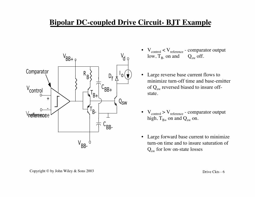
Transformer-coupled BJT Drive
Qsw
VBB+
Vd
I o
VBB-
CBB-
CBB+
RB
TB+
TB-
Df
AC power in
Oscillator
Q Q
Vcontrol
Oscillator output
Vcontrol
Transformer primary voltage
Input to comparator
t
t
t
t
Fast signal diodes
High frequency transformer

Copyright © by John Wiley & Sons 2003 Drive Ckts - 12
Opto-Coupler Isolated MOSFET Drives
Qsw
VGG+Vd
I o
VGG-
CGG-
CGG+
R G
TB+
TB-
Df
Opto-coupler
AC power in
Signal from control electronics
Opto-coupler Signal from control electronics
Qsw
Vd
I o
R G
IC buffer amp with totem pole outputDS0026 or UC1706/07
CGG-
GG+V
CGG+
GG-V (Circuitry for isolateddc supplies not shown)

Copyright © by John Wiley & Sons 2003 Drive Ckts - 13
Isolated Drives Without Auxiliary DC Supplies- Proportional Flyback BJT Example
VBB
N3
2N1NQsw
T1
CpRp
ip i B
i C
• Regenerative circuit operation
• T1 on - current ip = VBB/Rp and Qsw off
• T1 turned off - stored energy in gapped transformer core induces positive base current iB in Qsw causing it to go activeand collector current iC begins to flow
• Regenerative action of transformer connections supplies abase current iB = N3iC/N2 which keeps Qsw on even with ip = 0
• T1 turned on - positive current ip causes a base currentiB = N3iC/N2 - N1ip/N2 in Qsw
• Initially ip quite large (ip(0+) = biB1(0+)) so Qsw turned off
• Circuit design must insure turn-off iB has adequate negative magnitude and duration
• Best suited for high frequency operation - lower volt-secondrequirements on transformer.
• Also best suited for limited variations in duty cycle

Copyright © by John Wiley & Sons 2003 Drive Ckts - 14
Isolated Drives Without Auxiliary DC Supplies- MOSFET Example
Buffer
vC+
Buffer output voltage
vC
vsec
+
vsec
duty ratioD= 0.5
vsec
Buffer output voltage
vC
duty ratioD= 0.3
t
t
t
t
VDD
VDD= (1 - D)
0
0
0
0
Most suitable for applicationswhere duty cycle D is 50% orless. Positive-going secondaryvoltage decreases as D increases.

Copyright © by John Wiley & Sons 2003 Drive Ckts - 15
Isolated Drive Without Auxiliary DC Supplies- MOSFET Example
Inverting Buffer
Noninverting Buffer
Vcontrol
Schmitttrigger
A
BC
VZVZ
vcap
vsec
vcapvsec
t
t
t
t
t
t
Vcontrol
vA
v C
v B
v BvA
(dotted)
Zener diode voltage VZmust be less than negativepulse out of transformersecondary or pulse will notreach MOSFET gate to turnit off.
Copyright © by John Wiley & Sons 2003 Drive Ckts - 16
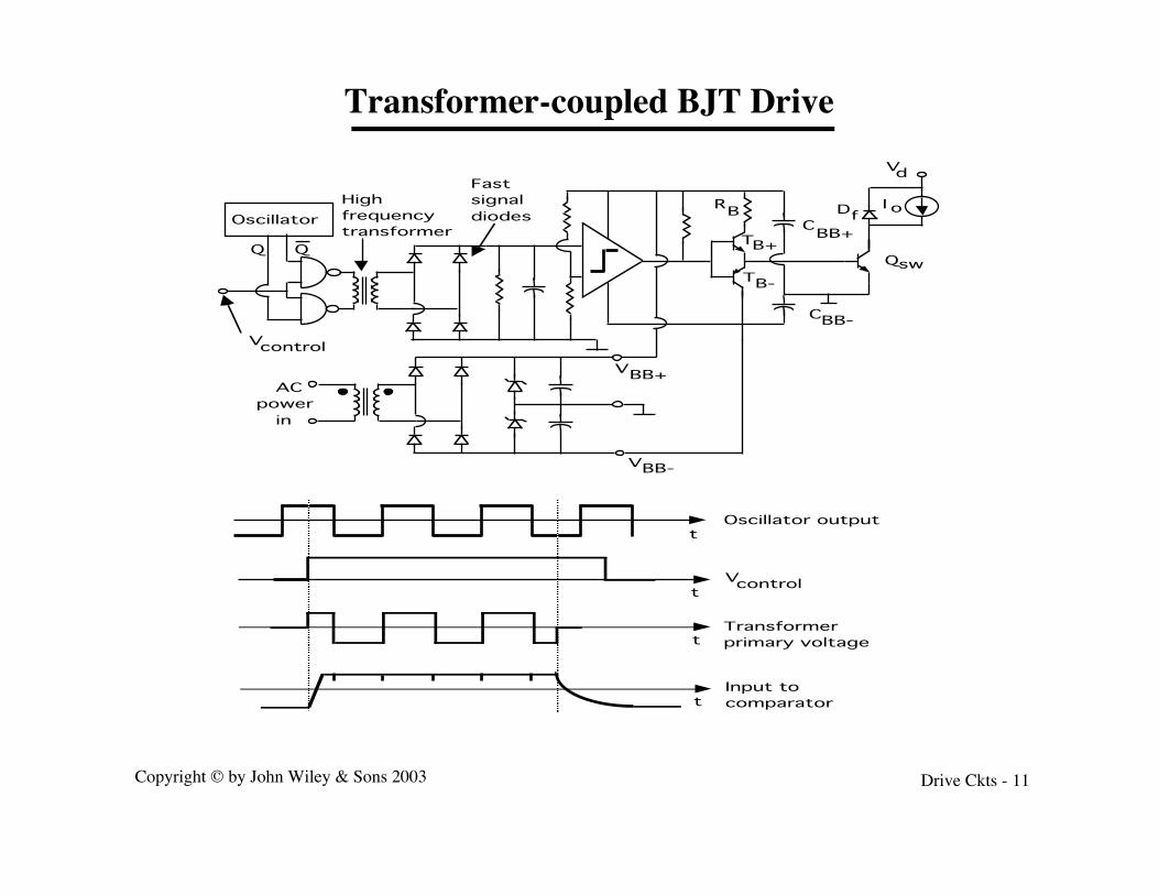
Isolated Drive Without Auxiliary DC Supplies- MOSFET Example
Buffer
Buffer
4011
4047oscillator
(1 MHz)
Q
Qvcontrol
7555RG
1svv2sDB
vcontrol
vQ
vQ
v2s
v1s
C2C1R2
+
-
+
-
vtrans+
-
vtrans
22
Decay of voltage on C via R
C charges up to a positive voltage at power-up and remains there. D prevents discharge
1
B
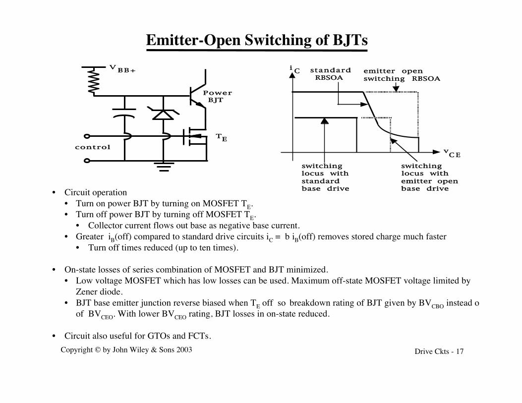
Copyright © by John Wiley & Sons 2003 Drive Ckts - 17
Emitter-Open Switching of BJTsV BB+
control
Power BJT
TE
standard RBSOA
emitter openswitching RBSOA
i C
vCE
switching locus withemitter open base drive
switching locus withstandard base drive• Circuit operation
• Turn on power BJT by turning on MOSFET TE.• Turn off power BJT by turning off MOSFET TE.
• Collector current flows out base as negative base current. • Greater iB(off) compared to standard drive circuits iC = b iB(off) removes stored charge much faster
• Turn off times reduced (up to ten times).
• On-state losses of series combination of MOSFET and BJT minimized.• Low voltage MOSFET which has low losses can be used. Maximum off-state MOSFET voltage limited by
Zener diode.• BJT base emitter junction reverse biased when TE off so breakdown rating of BJT given by BVCBO instead o
of BVCEO. With lower BVCEO rating, BJT losses in on-state reduced.
• Circuit also useful for GTOs and FCTs.

Copyright © by John Wiley & Sons 2003 Drive Ckts - 18
Thyristor Gate Drive Circuit
Line Voltage
zero crossing detection
DC power supply for gate trigger circuit
DelayAngleBlock
PulseAmplifier
InputControlSignal
ControlLogicGround
gate pulseisolationtransformers
gate pulseisolationtransformers
1
23
4
Delay angle block iscommercially availableintegrated circuit -TCA780 circuit family

Copyright © by John Wiley & Sons 2003 Drive Ckts - 19
Thyristor Gate Drive Circuit (cont.)
Control of 3 & 4
Control of 1 & 2
Controlvoltage
Ramp
TransformerLine Voltage
aaa
Trigger signal
DfRG
TG
15 VD1
Thyristor gate drive waveforms
Gate pulse amplifier
Copyright © by John Wiley & Sons 2003 Drive Ckts - 20
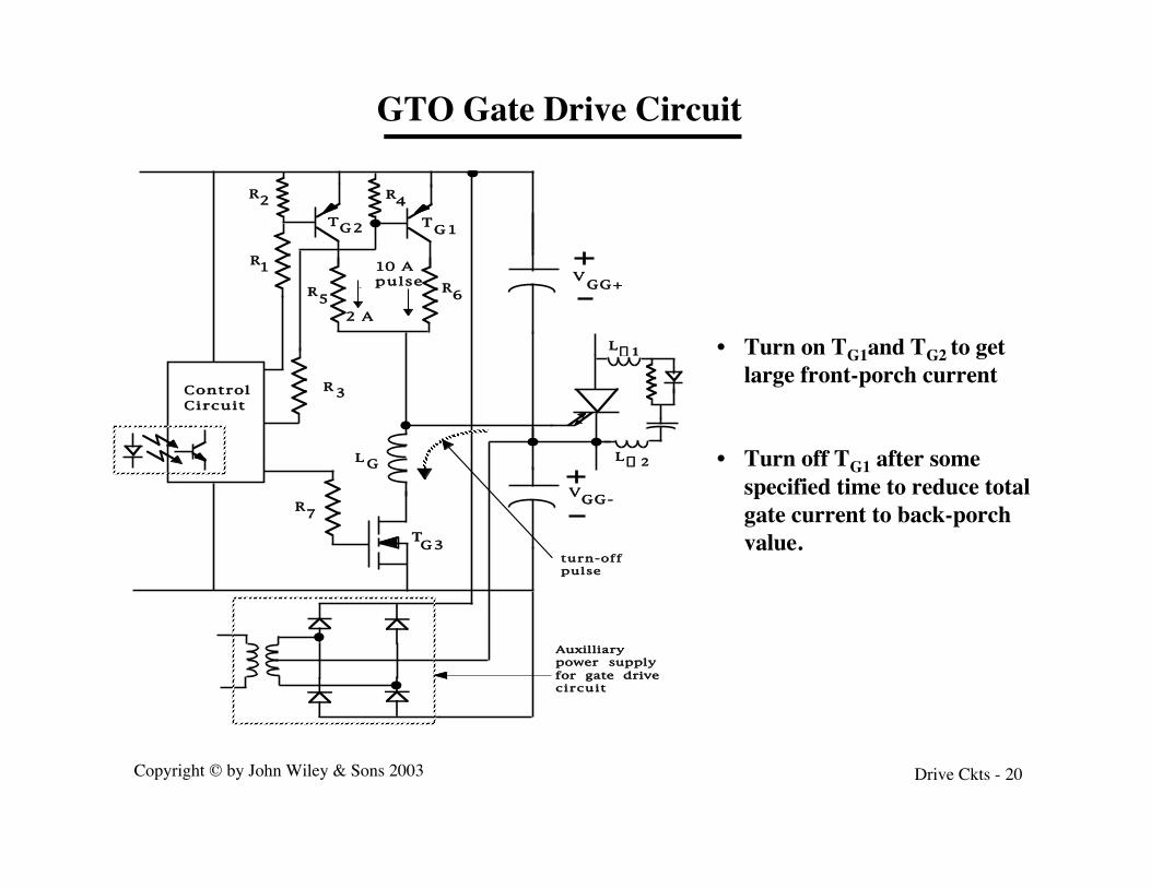
GTO Gate Drive Circuit
Auxilliary power supplyfor gate drivecircuit
TG3
ControlCircuit
R1
R2
R3
R4
R5R6
R7
TG1TG2
2 A
10 Apulse V
GG+
VGG-
L G
turn-offpulse
Ls 1
L s 2
• Turn on TG1and TG2 to get large front-porch current
• Turn off TG1 after some specified time to reduce totalgate current to back-porch value.
Copyright © by John Wiley & Sons 2003 Drive Ckts - 21
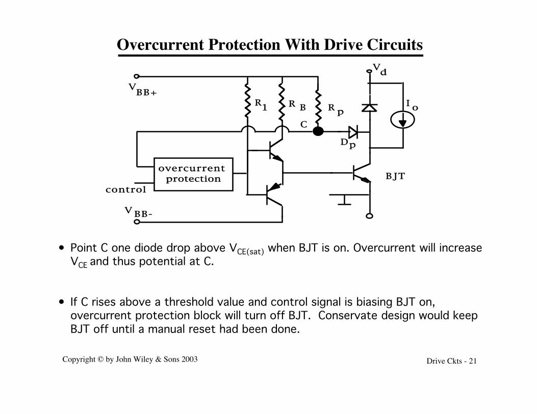
Overcurrent Protection With Drive Circuits
VBB+I o
BJT
V BB-
R p
Dp
C
overcurrent protection
control
R BR1
Vd
• Point C one diode drop above VCE(sat) when BJT is on. Overcurrent will increase VCE and thus potential at C.
• If C rises above a threshold value and control signal is biasing BJT on, overcurrent protection block will turn off BJT. Conservate design would keep BJT off until a manual reset had been done.

Copyright © by John Wiley & Sons 2003 Drive Ckts - 22
Limiting Overcurrents by Limiting On-state Base Current
Vd
+
-
DFI o
Cd• Stepdown converter with short curcuit at t = t sc
i C
v CE
IC,scIC(on)max
IB,max
Vin t sc
i C
t
• Overcurrent limited to IC(on)max < IC,sc by keeping IB,max < IC,sc/b
• IC,sc = maximum allowable instantaneous collector current
• Same approach can be used with MOSFETs and IGBTs. VGS mustbe restricted to keep drain current tosafe values.

Copyright © by John Wiley & Sons 2003 Drive Ckts - 23
Blanking Times in Bridge Circuit Drives
-
+ T+
T-
Vd Io
• Turn off T+ before turning on T- in order to avoid cross -conduction (shorting out of Vd)
Vcontrol, T+
Optocoupler or transformer
Optocoupler or transformer
Control for converter leg
Vcontrol, T-
V1+
V1 -
signal ground
Vcontrol, T+
Vcontrol, T-
V1 -
V1+
Vcontrol, bridge
blanking time
collector current
blanking time
deadtime
deadtime

Copyright © by John Wiley & Sons 2003 Drive Ckts - 24
Drive Circuit Waveshaping for Improved Operation
TB+
TB-
Das
D1
D2
V BB+
VBB-
QswA
E
R B• Anti-saturation diode Das keeps Qsw active.
• VAE = VBE(on) + VD1 = VCE(on) + Vdas• VCE(on) = VBE(on) > VCE(sat) because VD1 = Vdas
• Ds provides path for negative base current at Qsw turn-off.
• Storage delay time at turn-off reduced but on-state losses increase slightly.
TB+
TB-
V BB+
VBB-
Qsw
RB Con
i B
i Bt
• Transient overdrive provided via C for faster turn-on of switch
on
• Same concept can be applied to MOSFET and IGBT drive circuits
Speed-up capacitors

Copyright © by John Wiley & Sons 2003 Drive Ckts - 25
Drive Circuit Waveshaping (cont.)
TB+
TB-
V BB+
VBB-
L off
R B
Qsw
i B
TB+
TB-
V BB+
VBB-
R B1
Qsw
i B
Front porch current Back
porch current
Gate/base current
t
B2R
Control
Back porch current
Front porch current
Controlled rate of change of turn-off base current
• Excessively long collector current tailing time at BJT turn-off ifdiB(off)/dt is too large.
• Inductor Loff restricts diB(off)/dt to - VBB/Loff
Front porch, back porch gate/base currents atturn-on
• Faster turn-on without putting devicedeeply into on-state where turn-off delaytime will be substantially increased.
• Applicable to BJTs, MOSFETs, IGBTs, andGTOs.
Copyright © by John Wiley & Sons 2003 Drive Ckts - 26
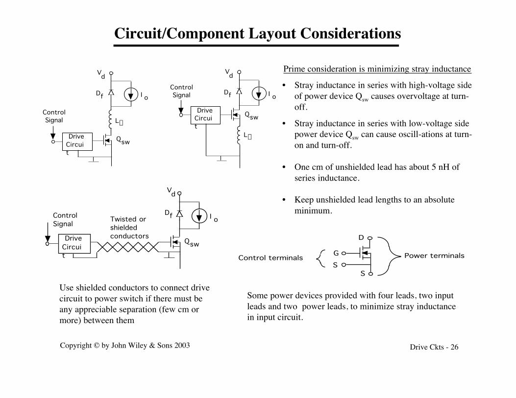
Circuit/Component Layout Considerations
I oDf
Qsw
Ls
Vd
DriveCircuit
Control Signal
I oDf
Qsw
Ls
Vd
DriveCircuit
Control Signal
Prime consideration is minimizing stray inductance
• Stray inductance in series with high-voltage sideof power device Qsw causes overvoltage at turn-off.
• Stray inductance in series with low-voltage sidepower device Qsw can cause oscill-ations at turn-on and turn-off.
• One cm of unshielded lead has about 5 nH of series inductance.
• Keep unshielded lead lengths to an absolute minimum.
I oDf
Qsw
Vd
DriveCircuit
Control Signal
Twisted or shielded conductors
Use shielded conductors to connect drivecircuit to power switch if there must beany appreciable separation (few cm ormore) between them
Control terminals Power terminalsG
SS
D
Some power devices provided with four leads, two inputleads and two power leads, to minimize stray inductancein input circuit.


![Ece-III-Analog Electronic Ckts [10es32]-Notes](https://img.pdfslide.us/doc/110x75/55cf9da2550346d033ae7b1a/ece-iii-analog-electronic-ckts-10es32-notes.jpg)


![Eee-III-Analog Electronic Ckts [10es32]-Solution](https://img.pdfslide.us/doc/110x75/5529d0b54a7959fa768b45d8/eee-iii-analog-electronic-ckts-10es32-solution.jpg)