Embed Size (px)
Citation preview

Dream Tech International Ltd
DTM0660
product brochures
4000/6000 indexing
T-RMS Digital Multimeter ASIC
PDF file using a trial version of "pdfFactory Pro" created www.fineprint.cnPDF file using a trial version of "pdfFactory Pro" created www.fineprint.cn
Dream Tech International Ltd.
Eye record
Pages
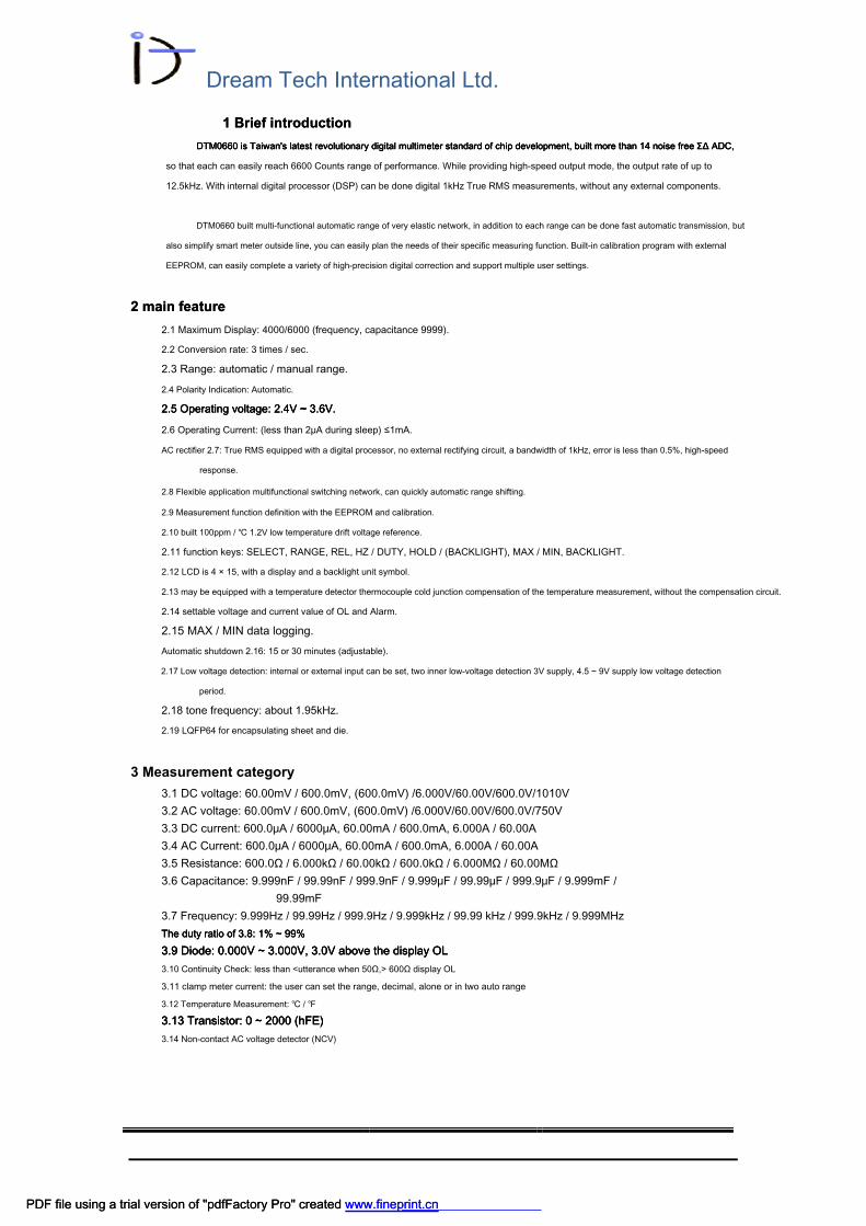
1 Introduction .................................................................. 32 Main features
............................................................ 33 measurement type applications
............................................................ ............................................................ 34 inside
the box 45 FIG ......................................................... 46 pin-out position of the package
sheet 47 in FIG ............................................. ...... pin description
...................................................... 58 69 key Specifications
............................................................ defined ............ ...................................................
810 other functions described ......................................................... 8 11 EEPROM
option setting ......... The method of correcting process .......................................... 912
13 13 ...................................................... application circuit and description ..................
..................... The liquid crystal display 1714 ......... 2915
......................................................... sheet package dimensions
...................................................... modify record
............................................................... 31 30 16
PDF file using a trial version of "pdfFactory Pro" created www.fineprint.cnPDF file using a trial version of "pdfFactory Pro" created www.fineprint.cn
Dream Tech International Ltd.
1 Brief introduction 1 Brief introduction
DTM0660 is Taiwan's latest revolutionary digital multimeter standard of chip development, built more than 14 noise free ΣΔ ADC, DTM0660 is Taiwan's latest revolutionary digital multimeter standard of chip development, built more than 14 noise free ΣΔ ADC, DTM0660 is Taiwan's latest revolutionary digital multimeter standard of chip development, built more than 14 noise free ΣΔ ADC,
so that each can easily reach 6600 Counts range of performance. While providing high-speed output mode, the output rate of up to
12.5kHz. With internal digital processor (DSP) can be done digital 1kHz True RMS measurements, without any external components.
DTM0660 built multi-functional automatic range of very elastic network, in addition to each range can be done fast automatic transmission, but
also simplify smart meter outside line, you can easily plan the needs of their specific measuring function. Built-in calibration program with external
EEPROM, can easily complete a variety of high-precision digital correction and support multiple user settings.
2 main feature2 main feature
2.1 Maximum Display: 4000/6000 (frequency, capacitance 9999).
2.2 Conversion rate: 3 times / sec.
2.3 Range: automatic / manual range.
2.4 Polarity Indication: Automatic.
2.5 Operating voltage: 2.4V ~ 3.6V. 2.5 Operating voltage: 2.4V ~ 3.6V. 2.5 Operating voltage: 2.4V ~ 3.6V.
2.6 Operating Current: (less than 2μA during sleep) ≤1mA.
AC rectifier 2.7: True RMS equipped with a digital processor, no external rectifying circuit, a bandwidth of 1kHz, error is less than 0.5%, high-speed
response.
2.8 Flexible application multifunctional switching network, can quickly automatic range shifting.
2.9 Measurement function definition with the EEPROM and calibration.
2.10 built 100ppm / ℃ 1.2V low temperature drift voltage reference.
2.11 function keys: SELECT, RANGE, REL, HZ / DUTY, HOLD / (BACKLIGHT), MAX / MIN, BACKLIGHT.
2.12 LCD is 4 × 15, with a display and a backlight unit symbol.
2.13 may be equipped with a temperature detector thermocouple cold junction compensation of the temperature measurement, without the compensation circuit.
2.14 settable voltage and current value of OL and Alarm.
2.15 MAX / MIN data logging.
Automatic shutdown 2.16: 15 or 30 minutes (adjustable).
2.17 Low voltage detection: internal or external input can be set, two inner low-voltage detection 3V supply, 4.5 ~ 9V supply low voltage detection
period.
2.18 tone frequency: about 1.95kHz.
2.19 LQFP64 for encapsulating sheet and die.
3 Measurement category
3.1 DC voltage: 60.00mV / 600.0mV, (600.0mV) /6.000V/60.00V/600.0V/1010V
3.2 AC voltage: 60.00mV / 600.0mV, (600.0mV) /6.000V/60.00V/600.0V/750V
3.3 DC current: 600.0μA / 6000μA, 60.00mA / 600.0mA, 6.000A / 60.00A
3.4 AC Current: 600.0μA / 6000μA, 60.00mA / 600.0mA, 6.000A / 60.00A
3.5 Resistance: 600.0Ω / 6.000kΩ / 60.00kΩ / 600.0kΩ / 6.000MΩ / 60.00MΩ
3.6 Capacitance: 9.999nF / 99.99nF / 999.9nF / 9.999μF / 99.99μF / 999.9μF / 9.999mF /
99.99mF
3.7 Frequency: 9.999Hz / 99.99Hz / 999.9Hz / 9.999kHz / 99.99 kHz / 999.9kHz / 9.999MHz
The duty ratio of 3.8: 1% ~ 99% The duty ratio of 3.8: 1% ~ 99% The duty ratio of 3.8: 1% ~ 99%
3.9 Diode: 0.000V ~ 3.000V, 3.0V above the display OL 3.9 Diode: 0.000V ~ 3.000V, 3.0V above the display OL 3.9 Diode: 0.000V ~ 3.000V, 3.0V above the display OL
3.10 Continuity Check: less than <utterance when 50Ω,> 600Ω display OL
3.11 clamp meter current: the user can set the range, decimal, alone or in two auto range
3.12 Temperature Measurement: ℃ / ℉
3.13 Transistor: 0 ~ 2000 (hFE) 3.13 Transistor: 0 ~ 2000 (hFE) 3.13 Transistor: 0 ~ 2000 (hFE)
3.14 Non-contact AC voltage detector (NCV)
PDF file using a trial version of "pdfFactory Pro" created www.fineprint.cnPDF file using a trial version of "pdfFactory Pro" created www.fineprint.cn
Dream Tech International Ltd.
4 Applications
4.1 autoranging / manual range handheld digital multimeter.
4.2 autoranging / manual range Card Digital Meter.
4.3 auto-range digital multimeter pen.
4.4 autoranging clamp meter.
4.5 Digital Panel Meters.
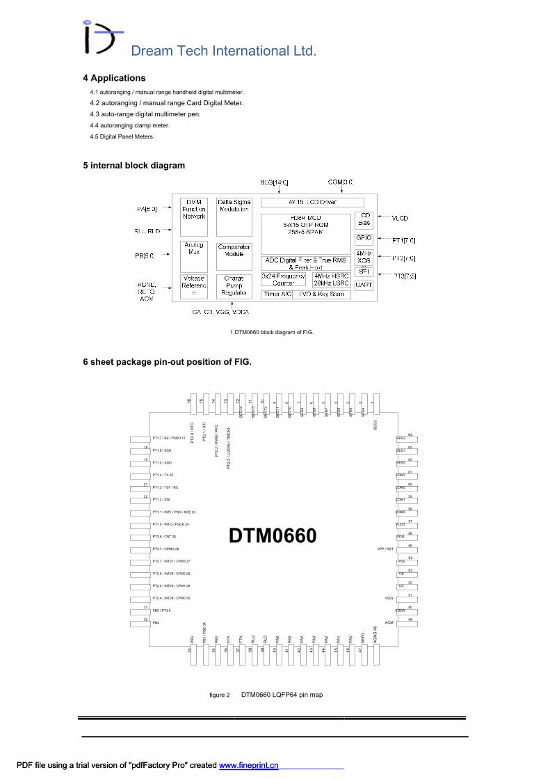
5 internal block diagram
1 DTM0660 block diagram of FIG.
6 sheet package pin-out position of FIG.
ACM
49
VDDA
50
VSS
54
VGG
51
CA
52
CB
53
VPP / RST
55
VDD
56
VLCD
57
COM0
58
COM1
59
COM2
60
COM3
61
SEG0
62
SEG1
63
SEG2
64
PT1.7 / BZ / PSDO 17
PT1.6 / SCK
18
PT1.5 / SDO
19
PT1.4 / TX 20
PT1.3 / TST / RC
21
PT1.2 / SDI
22
PT1.1 / INT1 / PSD / SCE 23
PT1.0 / INTO / PSCK 24
PT3.6 / CNT 25
PT3.7 / CPMO 26
PT2.7 / INT27 / CPM3 27
PT2.6 / INT26 / CPM2 28
PT2.5 / INT25 / CPM1 29
PT2.4 / INT24 / CPM0 30
PB5 / PT3.5
31
PB4
32
DTM0660
figure 2 DTM0660 LQFP64 pin map
PDF file using a trial version of "pdfFactory Pro" created www.fineprint.cnPDF file using a trial version of "pdfFactory Pro" created www.fineprint.cn
PB
3
33
PB
1 / P
B2
3
4
PB
0
35
FT
P
36
FT
N
37
RL
U
38
RL
D
39
PA
6
40
PA
5
41
PA
4
42
PA
3
43
PA
2
44
PA
1
45
PA
0
46
RE
FO
47
AG
ND
48
SE
G3
1
SE
G4
2
SE
G5
3
SE
G6
4
SE
G7
5
SE
G8
6
SE
G9
7
SE
G1
0
8
SE
G1
1
9
SE
G1
2
10
SE
G1
3
11
SE
G1
4
12
PT
2.3 / LV
DIN
/ T
MC
KI
13
PT
2.2
/ P
WM
/ P
FD
14
PT
2.1 / X
TI
15
PT
2.0 / X
TO
16
Dream Tech International Ltd.
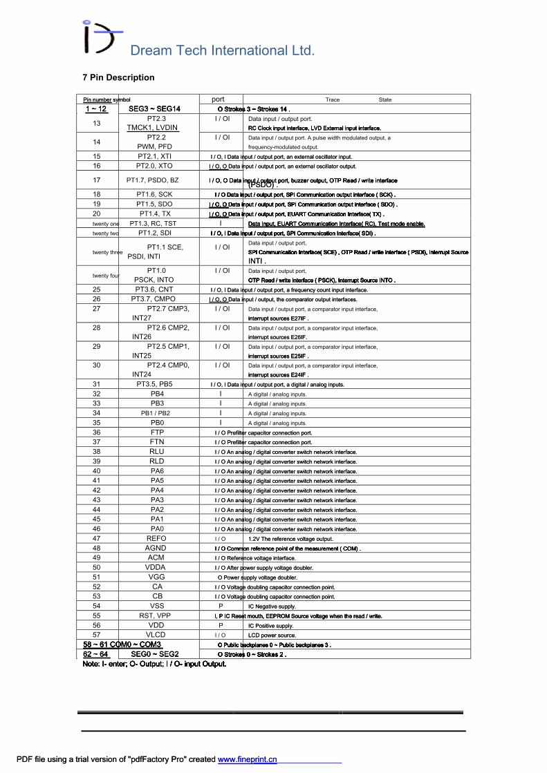
7 Pin Description
Pin number symbolPin number symbol port Trace State
1 ~ 12 1 ~ 12 1 ~ 12 SEG3 ~ SEG14 SEG3 ~ SEG14 SEG3 ~ SEG14 O Strokes 3 ~ Strokes 14 .O Strokes 3 ~ Strokes 14 .O Strokes 3 ~ Strokes 14 .O Strokes 3 ~ Strokes 14 .O Strokes 3 ~ Strokes 14 .O Strokes 3 ~ Strokes 14 .O Strokes 3 ~ Strokes 14 .
13
PT2.3
TMCK1, LVDIN
I / OI Data input / output port.
RC Clock input interface, LVD External input interface.RC Clock input interface, LVD External input interface.RC Clock input interface, LVD External input interface.RC Clock input interface, LVD External input interface.
14
PT2.2
PWM, PFD
I / OI Data input / output port. A pulse width modulated output, a
frequency-modulated output.
15 PT2.1, XTI I / O, I Data input / output port, an external oscillator input.I / O, I Data input / output port, an external oscillator input.
16 PT2.0, XTO I / O, O Data input / output port, an external oscillator output.I / O, O Data input / output port, an external oscillator output.
17 PT1.7, PSDO, BZ I / O, O Data input / output port, buzzer output, OTP Read / write interfaceI / O, O Data input / output port, buzzer output, OTP Read / write interfaceI / O, O Data input / output port, buzzer output, OTP Read / write interfaceI / O, O Data input / output port, buzzer output, OTP Read / write interface
(PSDO) .(PSDO) .
18 PT1.6, SCK I / O Data input / output port, SPI Communication output interface ( SCK) .I / O Data input / output port, SPI Communication output interface ( SCK) .I / O Data input / output port, SPI Communication output interface ( SCK) .I / O Data input / output port, SPI Communication output interface ( SCK) .I / O Data input / output port, SPI Communication output interface ( SCK) .I / O Data input / output port, SPI Communication output interface ( SCK) .
19 PT1.5, SDO I / O, O Data input / output port, SPI Communication output interface ( SDO) .I / O, O Data input / output port, SPI Communication output interface ( SDO) .I / O, O Data input / output port, SPI Communication output interface ( SDO) .I / O, O Data input / output port, SPI Communication output interface ( SDO) .I / O, O Data input / output port, SPI Communication output interface ( SDO) .I / O, O Data input / output port, SPI Communication output interface ( SDO) .
20 PT1.4, TX I / O, O Data input / output port, EUART Communication Interface( TX) .I / O, O Data input / output port, EUART Communication Interface( TX) .I / O, O Data input / output port, EUART Communication Interface( TX) .I / O, O Data input / output port, EUART Communication Interface( TX) .I / O, O Data input / output port, EUART Communication Interface( TX) .I / O, O Data input / output port, EUART Communication Interface( TX) .
twenty one PT1.3, RC, TST I Data input, EUART Communication Interface( RC), Test mode enable.Data input, EUART Communication Interface( RC), Test mode enable.Data input, EUART Communication Interface( RC), Test mode enable.Data input, EUART Communication Interface( RC), Test mode enable.Data input, EUART Communication Interface( RC), Test mode enable.
twenty two PT1.2, SDI I / O, I Data input / output port, SPI Communication Interface( SDI) .I / O, I Data input / output port, SPI Communication Interface( SDI) .I / O, I Data input / output port, SPI Communication Interface( SDI) .I / O, I Data input / output port, SPI Communication Interface( SDI) .I / O, I Data input / output port, SPI Communication Interface( SDI) .I / O, I Data input / output port, SPI Communication Interface( SDI) .
twenty three
PT1.1 SCE,
PSDI, INTI
I / OI
Data input / output port,
SPI Communication Interface( SCE) , OTP Read / write interface ( PSDI), Interrupt SourceSPI Communication Interface( SCE) , OTP Read / write interface ( PSDI), Interrupt SourceSPI Communication Interface( SCE) , OTP Read / write interface ( PSDI), Interrupt SourceSPI Communication Interface( SCE) , OTP Read / write interface ( PSDI), Interrupt SourceSPI Communication Interface( SCE) , OTP Read / write interface ( PSDI), Interrupt SourceSPI Communication Interface( SCE) , OTP Read / write interface ( PSDI), Interrupt SourceSPI Communication Interface( SCE) , OTP Read / write interface ( PSDI), Interrupt SourceSPI Communication Interface( SCE) , OTP Read / write interface ( PSDI), Interrupt Source
INTI .INTI .
twenty four
PT1.0
PSCK, INTO
I / OI Data input / output port,
OTP Read / write interface ( PSCK), Interrupt Source INTO .OTP Read / write interface ( PSCK), Interrupt Source INTO .OTP Read / write interface ( PSCK), Interrupt Source INTO .OTP Read / write interface ( PSCK), Interrupt Source INTO .OTP Read / write interface ( PSCK), Interrupt Source INTO .OTP Read / write interface ( PSCK), Interrupt Source INTO .
25 PT3.6, CNT I / O, I Data input / output port, a frequency count input interface.I / O, I Data input / output port, a frequency count input interface.
26 PT3.7, CMPO I / O, O Data input / output, the comparator output interfaces.I / O, O Data input / output, the comparator output interfaces.
27 PT2.7 CMP3,
INT27
I / OI Data input / output port, a comparator input interface,
interrupt sources E27IF .interrupt sources E27IF .interrupt sources E27IF .
28 PT2.6 CMP2,
INT26
I / OI Data input / output port, a comparator input interface,
interrupt sources E26IF. interrupt sources E26IF.
29 PT2.5 CMP1,
INT25
I / OI Data input / output port, a comparator input interface,
interrupt sources E25IF .interrupt sources E25IF .interrupt sources E25IF .
30 PT2.4 CMP0,
INT24
I / OI Data input / output port, a comparator input interface,
interrupt sources E24IF .interrupt sources E24IF .interrupt sources E24IF .
31 PT3.5, PB5 I / O, I Data input / output port, a digital / analog inputs.I / O, I Data input / output port, a digital / analog inputs.
32 PB4 I A digital / analog inputs.
33 PB3 I A digital / analog inputs.
34 PB1 / PB2 I A digital / analog inputs.
35 PB0 I A digital / analog inputs.
36 FTP I / O Prefilter capacitor connection port.I / O Prefilter capacitor connection port.
37 FTN I / O Prefilter capacitor connection port.I / O Prefilter capacitor connection port.
38 RLU I / O An analog / digital converter switch network interface.I / O An analog / digital converter switch network interface.
39 RLD I / O An analog / digital converter switch network interface.I / O An analog / digital converter switch network interface.
40 PA6 I / O An analog / digital converter switch network interface.I / O An analog / digital converter switch network interface.
41 PA5 I / O An analog / digital converter switch network interface.I / O An analog / digital converter switch network interface.
42 PA4 I / O An analog / digital converter switch network interface.I / O An analog / digital converter switch network interface.
43 PA3 I / O An analog / digital converter switch network interface.I / O An analog / digital converter switch network interface.
44 PA2 I / O An analog / digital converter switch network interface.I / O An analog / digital converter switch network interface.
45 PA1 I / O An analog / digital converter switch network interface.I / O An analog / digital converter switch network interface.
46 PA0 I / O An analog / digital converter switch network interface.I / O An analog / digital converter switch network interface.
47 REFO I / O 1.2V The reference voltage output.1.2V The reference voltage output.
48 AGND I / O Common reference point of the measurement ( COM) .I / O Common reference point of the measurement ( COM) .I / O Common reference point of the measurement ( COM) .I / O Common reference point of the measurement ( COM) .
49 ACM I / O Reference voltage interface.I / O Reference voltage interface.
50 VDDA I / O After power supply voltage doubler.I / O After power supply voltage doubler.
51 VGG O Power supply voltage doubler.O Power supply voltage doubler.
52 CA I / O Voltage doubling capacitor connection point.I / O Voltage doubling capacitor connection point.
53 CB I / O Voltage doubling capacitor connection point.I / O Voltage doubling capacitor connection point.
54 VSS P IC Negative supply.IC Negative supply.
55 RST, VPP I, P IC Reset mouth, EEPROM Source voltage when the read / write.I, P IC Reset mouth, EEPROM Source voltage when the read / write.I, P IC Reset mouth, EEPROM Source voltage when the read / write.I, P IC Reset mouth, EEPROM Source voltage when the read / write.
56 VDD P IC Positive supply.IC Positive supply.
57 VLCD I / O LCD power source.LCD power source.
58 ~ 61 COM0 ~ COM3 58 ~ 61 COM0 ~ COM3 58 ~ 61 COM0 ~ COM3 58 ~ 61 COM0 ~ COM3 58 ~ 61 COM0 ~ COM3 O Public backplanes 0 ~ Public backplanes 3 .O Public backplanes 0 ~ Public backplanes 3 .O Public backplanes 0 ~ Public backplanes 3 .O Public backplanes 0 ~ Public backplanes 3 .O Public backplanes 0 ~ Public backplanes 3 .O Public backplanes 0 ~ Public backplanes 3 .O Public backplanes 0 ~ Public backplanes 3 .
62 ~ 64 62 ~ 64 62 ~ 64 SEG0 ~ SEG2 SEG0 ~ SEG2 SEG0 ~ SEG2 O Strokes 0 ~ Strokes 2 .O Strokes 0 ~ Strokes 2 .O Strokes 0 ~ Strokes 2 .O Strokes 0 ~ Strokes 2 .O Strokes 0 ~ Strokes 2 .O Strokes 0 ~ Strokes 2 .O Strokes 0 ~ Strokes 2 .
Note: I- enter; O- Output; I / O- input Output.Note: I- enter; O- Output; I / O- input Output.Note: I- enter; O- Output; I / O- input Output.Note: I- enter; O- Output; I / O- input Output.Note: I- enter; O- Output; I / O- input Output.Note: I- enter; O- Output; I / O- input Output.Note: I- enter; O- Output; I / O- input Output.
PDF file using a trial version of "pdfFactory Pro" created www.fineprint.cnPDF file using a trial version of "pdfFactory Pro" created www.fineprint.cn

Dream Tech International Ltd.
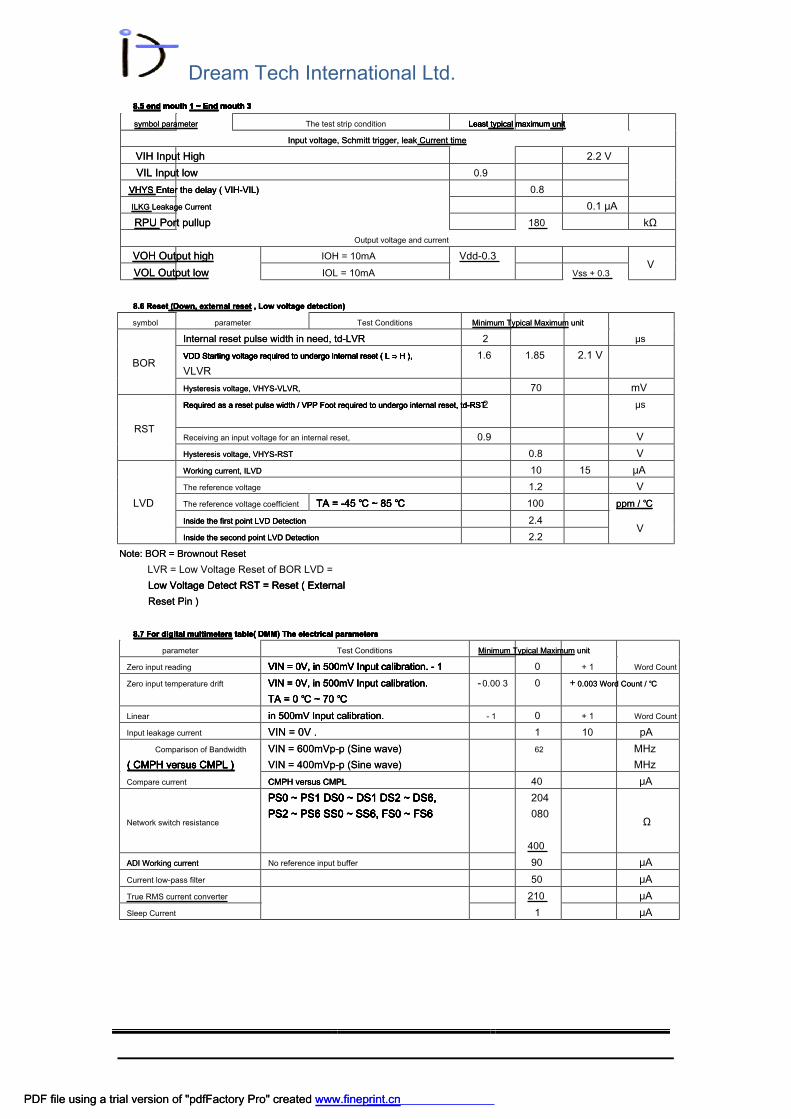
8 Technical Specifications (VDD = 3V, Ta = 25 ℃)8 Technical Specifications (VDD = 3V, Ta = 25 ℃)
8.1 Maximum rating8.1 Maximum rating
parameter symbol quota
voltage VDD (VDDA) -VSS (VSSA) -0.2V ~ 4V 0.2V ~ 4V 0.2V ~ 4V
Voltage may be applied to any range of foot -0.3V ~ VDD + 0.3V 0.3V ~ VDD + 0.3V 0.3V ~ VDD + 0.3V
Each leg receiving current protection diode ± 2mA
Storage temperature Tstg --50 ℃ ~ + 150 ℃--50 ℃ ~ + 150 ℃--50 ℃ ~ + 150 ℃--50 ℃ ~ + 150 ℃
Foot soldering temperature Temp 300 ℃300 ℃
Welding time Time 10 second10 second
Total power consumption 500mW
8.2 Recommended operating conditions8.2 Recommended operating conditions
symbol parameter The test strip condition Least Typical Maximum UnitLeast Typical Maximum Unit
VDD voltage
All peripheral components and CPU All peripheral components and CPU 2.2 3.6 V
Analog Peripheral Component 2.4 3.6
VSS voltage 0 0
XT External oscillationXT External oscillation
frequency
Clock crystal
VDD = 2.2V
ENXT [0] = 1
XTSP [0] = 0,
XTHSP [0] = 0
32.768kHz
Hz Ceramic oscillator
XTSP [0] = 1,
XTHSP [0] = 0
400k 8M
Quartz crystal
XTSP [0] = 1,
XTHSP [0] = 0
1M 8M
8.3 internal RC oscillation8.3 internal RC oscillation8.3 internal RC oscillation8.3 internal RC oscillation
symbol parameter The test strip condition Minimum Typical Maximum Units
HAO High speed oscillation frequencyHAO High speed oscillation frequency ENHAO [0] = 1 4 MHz
LPO Low power oscillator frequency VDD can LPO LPO Low power oscillator frequency VDD can LPO LPO Low power oscillator frequency VDD can LPO LPO Low power oscillator frequency VDD can LPO LPO Low power oscillator frequency VDD can LPO 32 kHz
8.4 V DD Total current8.4 V DD Total current8.4 V DD Total current
symbol parameter
The test strip condition The minimum typical maximum single
Place
IAM 1 Active mode 1 OSC_CY = 8MHz, OSC_HAO = off,
CPU_CK = 8MHz
1.34 2 mA
IAM 2 Active mode 2 OSC_CY = off, OSC_HAO = 4MHz,
CPU_CK = 4MHz
0.36 0.55 mA
IAM 3 Active mode 3 OSC_CY = off, OSC_HAO = 4MHz,
CPU_CK = 2MHz
0.2 0.3 mA
ILP1 Low Power 1 OSC_CY = 32768Hz, OSC_HAO = off,
CPU_CK = 16384Hz
7 12 μA
ILP2 Low Power 2 OSC_CY = off, OSC_HAO = off,
CPU_CK = LPO, Idle state
1.65 3 μA
ILP3 Low Power 3 OSC_CY = off, OSC_HAO = off,
CPU_CK = off, Sleep state
0.65 1.3 μA
PDF file using a trial version of "pdfFactory Pro" created www.fineprint.cnPDF file using a trial version of "pdfFactory Pro" created www.fineprint.cn
Dream Tech International Ltd.
8.5 end mouth 1 ~ End mouth 3 8.5 end mouth 1 ~ End mouth 3 8.5 end mouth 1 ~ End mouth 3 8.5 end mouth 1 ~ End mouth 3 8.5 end mouth 1 ~ End mouth 3 8.5 end mouth 1 ~ End mouth 3 8.5 end mouth 1 ~ End mouth 3
symbol parametersymbol parameter The test strip condition Least typical maximum unitLeast typical maximum unitLeast typical maximum unitLeast typical maximum unit
Input voltage, Schmitt trigger, leak Current timeInput voltage, Schmitt trigger, leak Current time
VIH Input HighVIH Input High 2.2 V
VIL Input lowVIL Input low 0.9
VHYS Enter the delay ( VIH-VIL) VHYS Enter the delay ( VIH-VIL) VHYS Enter the delay ( VIH-VIL) 0.8
ILKG Leakage CurrentILKG Leakage Current 0.1 μA
RPU Port pullupRPU Port pullup 180 kΩ
Output voltage and current
VOH Output highVOH Output high IOH = 10mA Vdd-0.3
V
VOL Output lowVOL Output low IOL = 10mA Vss + 0.3
8.6 Reset (Down, external reset , Low voltage detection)8.6 Reset (Down, external reset , Low voltage detection)8.6 Reset (Down, external reset , Low voltage detection)8.6 Reset (Down, external reset , Low voltage detection)
symbol parameter Test Conditions Minimum Typical Maximum unitMinimum Typical Maximum unit
BOR
Internal reset pulse width in need, td-LVR Internal reset pulse width in need, td-LVR 2 μs
VDD Starting voltage required to undergo internal reset ( L ⇒ H ),VDD Starting voltage required to undergo internal reset ( L ⇒ H ),VDD Starting voltage required to undergo internal reset ( L ⇒ H ),VDD Starting voltage required to undergo internal reset ( L ⇒ H ),VDD Starting voltage required to undergo internal reset ( L ⇒ H ),VDD Starting voltage required to undergo internal reset ( L ⇒ H ),
VLVR
1.6 1.85 2.1 V
Hysteresis voltage, VHYS-VLVR, Hysteresis voltage, VHYS-VLVR, 70 mV
RST
Required as a reset pulse width / VPP Foot required to undergo internal reset, td-RST Required as a reset pulse width / VPP Foot required to undergo internal reset, td-RST Required as a reset pulse width / VPP Foot required to undergo internal reset, td-RST Required as a reset pulse width / VPP Foot required to undergo internal reset, td-RST 2 μs
Receiving an input voltage for an internal reset, 0.9 V
Hysteresis voltage, VHYS-RST Hysteresis voltage, VHYS-RST 0.8 V
LVD
Working current, ILVD Working current, ILVD 10 15 μA
The reference voltage 1.2 V
The reference voltage coefficient TA = -45 ℃ ~ 85 ℃TA = -45 ℃ ~ 85 ℃TA = -45 ℃ ~ 85 ℃TA = -45 ℃ ~ 85 ℃ 100 ppm / ℃ppm / ℃
Inside the first point LVD DetectionInside the first point LVD DetectionInside the first point LVD Detection 2.4
V
Inside the second point LVD DetectionInside the second point LVD DetectionInside the second point LVD Detection 2.2
Note: BOR = Brownout Reset Note: BOR = Brownout Reset
LVR = Low Voltage Reset of BOR LVD =
Low Voltage Detect RST = Reset ( External Low Voltage Detect RST = Reset ( External Low Voltage Detect RST = Reset ( External
Reset Pin )Reset Pin )
8.7 For digital multimeters table( DMM) The electrical parameters8.7 For digital multimeters table( DMM) The electrical parameters8.7 For digital multimeters table( DMM) The electrical parameters8.7 For digital multimeters table( DMM) The electrical parameters8.7 For digital multimeters table( DMM) The electrical parameters
parameter Test Conditions Minimum Typical Maximum unitMinimum Typical Maximum unit
Zero input reading VIN = 0V, in 500mV Input calibration. - 1 VIN = 0V, in 500mV Input calibration. - 1 VIN = 0V, in 500mV Input calibration. - 1 VIN = 0V, in 500mV Input calibration. - 1 VIN = 0V, in 500mV Input calibration. - 1 VIN = 0V, in 500mV Input calibration. - 1 0 + 1 Word Count
Zero input temperature drift VIN = 0V, in 500mV Input calibration.VIN = 0V, in 500mV Input calibration.VIN = 0V, in 500mV Input calibration.VIN = 0V, in 500mV Input calibration.
TA = 0 ℃ ~ 70 ℃TA = 0 ℃ ~ 70 ℃TA = 0 ℃ ~ 70 ℃TA = 0 ℃ ~ 70 ℃
-0.00 3 0 + 0.003 Word Count / ℃0.003 Word Count / ℃
Linear in 500mV Input calibration.in 500mV Input calibration.in 500mV Input calibration. - 1 0 + 1 Word Count
Input leakage current VIN = 0V .VIN = 0V . 1 10 pA
Comparison of Bandwidth
( CMPH versus CMPL )( CMPH versus CMPL )( CMPH versus CMPL )( CMPH versus CMPL )( CMPH versus CMPL )
VIN = 600mVp-p (Sine wave)VIN = 600mVp-p (Sine wave)
VIN = 400mVp-p (Sine wave)VIN = 400mVp-p (Sine wave)
62 MHz
MHz
Compare current CMPH versus CMPL CMPH versus CMPL CMPH versus CMPL 40 μA
Network switch resistance
PS0 ~ PS1 DS0 ~ DS1 DS2 ~ DS6, PS0 ~ PS1 DS0 ~ DS1 DS2 ~ DS6, PS0 ~ PS1 DS0 ~ DS1 DS2 ~ DS6, PS0 ~ PS1 DS0 ~ DS1 DS2 ~ DS6, PS0 ~ PS1 DS0 ~ DS1 DS2 ~ DS6, PS0 ~ PS1 DS0 ~ DS1 DS2 ~ DS6, PS0 ~ PS1 DS0 ~ DS1 DS2 ~ DS6,
PS2 ~ PS6 SS0 ~ SS6, FS0 ~ FS6 PS2 ~ PS6 SS0 ~ SS6, FS0 ~ FS6 PS2 ~ PS6 SS0 ~ SS6, FS0 ~ FS6 PS2 ~ PS6 SS0 ~ SS6, FS0 ~ FS6 PS2 ~ PS6 SS0 ~ SS6, FS0 ~ FS6 PS2 ~ PS6 SS0 ~ SS6, FS0 ~ FS6 PS2 ~ PS6 SS0 ~ SS6, FS0 ~ FS6
204
080
400
Ω
ADI Working currentADI Working current No reference input buffer 90 μA
Current low-pass filter 50 μA
True RMS current converter 210 μA
Sleep Current 1 μA
PDF file using a trial version of "pdfFactory Pro" created www.fineprint.cnPDF file using a trial version of "pdfFactory Pro" created www.fineprint.cn
Dream Tech International Ltd.
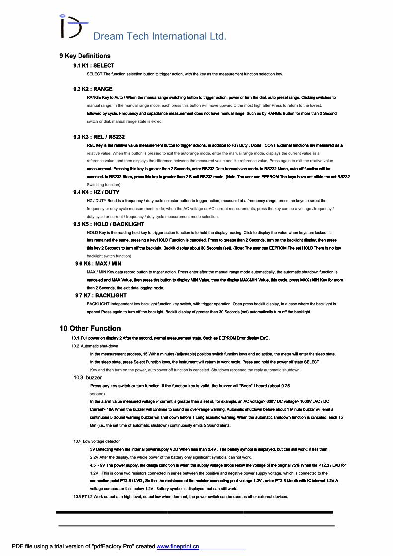
9 Key Definitions9 Key Definitions
9.1 K1 : SELECT 9.1 K1 : SELECT 9.1 K1 : SELECT
SELECT The function selection button to trigger action, with the key as the measurement function selection key.SELECT The function selection button to trigger action, with the key as the measurement function selection key.
9.2 K2 : RANGE 9.2 K2 : RANGE 9.2 K2 : RANGE
RANGE Key to Auto / When the manual range switching button to trigger action, power or turn the dial, auto preset range. Clicking switches to RANGE Key to Auto / When the manual range switching button to trigger action, power or turn the dial, auto preset range. Clicking switches to RANGE Key to Auto / When the manual range switching button to trigger action, power or turn the dial, auto preset range. Clicking switches to RANGE Key to Auto / When the manual range switching button to trigger action, power or turn the dial, auto preset range. Clicking switches to
manual range. In the manual range mode, each press this button will move upward to the most high after Press to return to the lowest,
followed by cycle. Frequency and capacitance measurement does not have manual range. Such as by RANGE Button for more than 2 Second followed by cycle. Frequency and capacitance measurement does not have manual range. Such as by RANGE Button for more than 2 Second followed by cycle. Frequency and capacitance measurement does not have manual range. Such as by RANGE Button for more than 2 Second followed by cycle. Frequency and capacitance measurement does not have manual range. Such as by RANGE Button for more than 2 Second followed by cycle. Frequency and capacitance measurement does not have manual range. Such as by RANGE Button for more than 2 Second
switch or dial, manual range state is exited.
9.3 K3 : REL / RS232 9.3 K3 : REL / RS232 9.3 K3 : REL / RS232
REL Key is the relative value measurement button to trigger actions, in addition to Hz / Duty , Diode , CONT External functions are measured as a REL Key is the relative value measurement button to trigger actions, in addition to Hz / Duty , Diode , CONT External functions are measured as a REL Key is the relative value measurement button to trigger actions, in addition to Hz / Duty , Diode , CONT External functions are measured as a REL Key is the relative value measurement button to trigger actions, in addition to Hz / Duty , Diode , CONT External functions are measured as a REL Key is the relative value measurement button to trigger actions, in addition to Hz / Duty , Diode , CONT External functions are measured as a REL Key is the relative value measurement button to trigger actions, in addition to Hz / Duty , Diode , CONT External functions are measured as a REL Key is the relative value measurement button to trigger actions, in addition to Hz / Duty , Diode , CONT External functions are measured as a REL Key is the relative value measurement button to trigger actions, in addition to Hz / Duty , Diode , CONT External functions are measured as a
relative value. When this button is pressed to exit the autorange mode, enter the manual range mode, displays the current value as a
reference value, and then displays the difference between the measured value and the reference value, Press again to exit the relative value
measurement. Pressing this key is greater than 2 Seconds, enter RS232 Data transmission mode. in RS232 Mode, auto-off function will be measurement. Pressing this key is greater than 2 Seconds, enter RS232 Data transmission mode. in RS232 Mode, auto-off function will be measurement. Pressing this key is greater than 2 Seconds, enter RS232 Data transmission mode. in RS232 Mode, auto-off function will be measurement. Pressing this key is greater than 2 Seconds, enter RS232 Data transmission mode. in RS232 Mode, auto-off function will be measurement. Pressing this key is greater than 2 Seconds, enter RS232 Data transmission mode. in RS232 Mode, auto-off function will be measurement. Pressing this key is greater than 2 Seconds, enter RS232 Data transmission mode. in RS232 Mode, auto-off function will be measurement. Pressing this key is greater than 2 Seconds, enter RS232 Data transmission mode. in RS232 Mode, auto-off function will be
canceled. in RS232 State, press this key is greater than 2 S exit RS232 mode. (Note: The user can EEPROM The keys have not within the set RS232canceled. in RS232 State, press this key is greater than 2 S exit RS232 mode. (Note: The user can EEPROM The keys have not within the set RS232canceled. in RS232 State, press this key is greater than 2 S exit RS232 mode. (Note: The user can EEPROM The keys have not within the set RS232canceled. in RS232 State, press this key is greater than 2 S exit RS232 mode. (Note: The user can EEPROM The keys have not within the set RS232canceled. in RS232 State, press this key is greater than 2 S exit RS232 mode. (Note: The user can EEPROM The keys have not within the set RS232canceled. in RS232 State, press this key is greater than 2 S exit RS232 mode. (Note: The user can EEPROM The keys have not within the set RS232canceled. in RS232 State, press this key is greater than 2 S exit RS232 mode. (Note: The user can EEPROM The keys have not within the set RS232canceled. in RS232 State, press this key is greater than 2 S exit RS232 mode. (Note: The user can EEPROM The keys have not within the set RS232canceled. in RS232 State, press this key is greater than 2 S exit RS232 mode. (Note: The user can EEPROM The keys have not within the set RS232canceled. in RS232 State, press this key is greater than 2 S exit RS232 mode. (Note: The user can EEPROM The keys have not within the set RS232
Switching function)
9.4 K4 : HZ / DUTY 9.4 K4 : HZ / DUTY 9.4 K4 : HZ / DUTY
HZ / DUTY Bond is a frequency / duty cycle selector button to trigger action, measured at a frequency range, press the keys to select the HZ / DUTY Bond is a frequency / duty cycle selector button to trigger action, measured at a frequency range, press the keys to select the
frequency or duty cycle measurement mode; when the AC voltage or AC current measurements, press the key can be a voltage / frequency /
duty cycle or current / frequency / duty cycle measurement mode selection.
9.5 K5 : HOLD / BACKLIGHT 9.5 K5 : HOLD / BACKLIGHT 9.5 K5 : HOLD / BACKLIGHT
HOLD Key is the reading hold key to trigger action function is to hold the display reading. Click to display the value when keys are locked, it HOLD Key is the reading hold key to trigger action function is to hold the display reading. Click to display the value when keys are locked, it
has remained the same, pressing a key HOLD Function is canceled. Press to greater than 2 Seconds, turn on the backlight display, then press has remained the same, pressing a key HOLD Function is canceled. Press to greater than 2 Seconds, turn on the backlight display, then press has remained the same, pressing a key HOLD Function is canceled. Press to greater than 2 Seconds, turn on the backlight display, then press has remained the same, pressing a key HOLD Function is canceled. Press to greater than 2 Seconds, turn on the backlight display, then press has remained the same, pressing a key HOLD Function is canceled. Press to greater than 2 Seconds, turn on the backlight display, then press
this key 2 Seconds to turn off the backlight. Backlit display about 30 Seconds (set). (Note: The user can EEPROM The set HOLD There is no key this key 2 Seconds to turn off the backlight. Backlit display about 30 Seconds (set). (Note: The user can EEPROM The set HOLD There is no key this key 2 Seconds to turn off the backlight. Backlit display about 30 Seconds (set). (Note: The user can EEPROM The set HOLD There is no key this key 2 Seconds to turn off the backlight. Backlit display about 30 Seconds (set). (Note: The user can EEPROM The set HOLD There is no key this key 2 Seconds to turn off the backlight. Backlit display about 30 Seconds (set). (Note: The user can EEPROM The set HOLD There is no key this key 2 Seconds to turn off the backlight. Backlit display about 30 Seconds (set). (Note: The user can EEPROM The set HOLD There is no key this key 2 Seconds to turn off the backlight. Backlit display about 30 Seconds (set). (Note: The user can EEPROM The set HOLD There is no key this key 2 Seconds to turn off the backlight. Backlit display about 30 Seconds (set). (Note: The user can EEPROM The set HOLD There is no key this key 2 Seconds to turn off the backlight. Backlit display about 30 Seconds (set). (Note: The user can EEPROM The set HOLD There is no key
backlight switch function)
9.6 K6 : MAX / MIN 9.6 K6 : MAX / MIN 9.6 K6 : MAX / MIN
MAX / MIN Key data record button to trigger action. Press enter after the manual range mode automatically, the automatic shutdown function is MAX / MIN Key data record button to trigger action. Press enter after the manual range mode automatically, the automatic shutdown function is
canceled and MAX Value, then press this button to display MIN Value, then the display MAX-MIN Value, this cycle. press MAX / MIN Key for more canceled and MAX Value, then press this button to display MIN Value, then the display MAX-MIN Value, this cycle. press MAX / MIN Key for more canceled and MAX Value, then press this button to display MIN Value, then the display MAX-MIN Value, this cycle. press MAX / MIN Key for more canceled and MAX Value, then press this button to display MIN Value, then the display MAX-MIN Value, this cycle. press MAX / MIN Key for more canceled and MAX Value, then press this button to display MIN Value, then the display MAX-MIN Value, this cycle. press MAX / MIN Key for more canceled and MAX Value, then press this button to display MIN Value, then the display MAX-MIN Value, this cycle. press MAX / MIN Key for more canceled and MAX Value, then press this button to display MIN Value, then the display MAX-MIN Value, this cycle. press MAX / MIN Key for more canceled and MAX Value, then press this button to display MIN Value, then the display MAX-MIN Value, this cycle. press MAX / MIN Key for more canceled and MAX Value, then press this button to display MIN Value, then the display MAX-MIN Value, this cycle. press MAX / MIN Key for more
than 2 Seconds, the exit data logging mode.than 2 Seconds, the exit data logging mode.than 2 Seconds, the exit data logging mode.
9.7 K7 : BACKLIGHT 9.7 K7 : BACKLIGHT 9.7 K7 : BACKLIGHT
BACKLIGHT Independent key backlight function key switch, with trigger operation. Open press backlit display, in a case where the backlight is BACKLIGHT Independent key backlight function key switch, with trigger operation. Open press backlit display, in a case where the backlight is
opened Press again to turn off the backlight. Backlit display of greater than 30 Seconds (set) automatically turn off the backlight.opened Press again to turn off the backlight. Backlit display of greater than 30 Seconds (set) automatically turn off the backlight.opened Press again to turn off the backlight. Backlit display of greater than 30 Seconds (set) automatically turn off the backlight.
10 Other Function10 Other Function10 Other Function
10.1 Full power on display 2 After the second, normal measurement state. Such as EEPROM Error display ErrE .10.1 Full power on display 2 After the second, normal measurement state. Such as EEPROM Error display ErrE .10.1 Full power on display 2 After the second, normal measurement state. Such as EEPROM Error display ErrE .10.1 Full power on display 2 After the second, normal measurement state. Such as EEPROM Error display ErrE .10.1 Full power on display 2 After the second, normal measurement state. Such as EEPROM Error display ErrE .10.1 Full power on display 2 After the second, normal measurement state. Such as EEPROM Error display ErrE .10.1 Full power on display 2 After the second, normal measurement state. Such as EEPROM Error display ErrE .10.1 Full power on display 2 After the second, normal measurement state. Such as EEPROM Error display ErrE .
10.2 Automatic shut-down10.2 Automatic shut-down
In the measurement process, 15 Within minutes (adjustable) position switch function keys and no action, the meter will enter the sleep state. In the measurement process, 15 Within minutes (adjustable) position switch function keys and no action, the meter will enter the sleep state. In the measurement process, 15 Within minutes (adjustable) position switch function keys and no action, the meter will enter the sleep state.
In the sleep state, press Select Function keys, the instrument will return to work mode. Press and hold the power off state SELECTIn the sleep state, press Select Function keys, the instrument will return to work mode. Press and hold the power off state SELECTIn the sleep state, press Select Function keys, the instrument will return to work mode. Press and hold the power off state SELECTIn the sleep state, press Select Function keys, the instrument will return to work mode. Press and hold the power off state SELECT
Key and then turn on the power, auto power off function is canceled. Shutdown reopened the reply automatic shutdown.
10.3 buzzer10.3 buzzer
Press any key switch or turn function, if the function key is valid, the buzzer will "Beep" I heard (about 0.25Press any key switch or turn function, if the function key is valid, the buzzer will "Beep" I heard (about 0.25Press any key switch or turn function, if the function key is valid, the buzzer will "Beep" I heard (about 0.25Press any key switch or turn function, if the function key is valid, the buzzer will "Beep" I heard (about 0.25
second).
In the alarm value measured voltage or current is greater than a set of, for example, an AC voltage> 600V DC voltage> 1000V , AC / DC In the alarm value measured voltage or current is greater than a set of, for example, an AC voltage> 600V DC voltage> 1000V , AC / DC In the alarm value measured voltage or current is greater than a set of, for example, an AC voltage> 600V DC voltage> 1000V , AC / DC In the alarm value measured voltage or current is greater than a set of, for example, an AC voltage> 600V DC voltage> 1000V , AC / DC In the alarm value measured voltage or current is greater than a set of, for example, an AC voltage> 600V DC voltage> 1000V , AC / DC
Current> 10A When the buzzer will continue to sound as over-range warning. Automatic shutdown before about 1 Minute buzzer will emit a Current> 10A When the buzzer will continue to sound as over-range warning. Automatic shutdown before about 1 Minute buzzer will emit a Current> 10A When the buzzer will continue to sound as over-range warning. Automatic shutdown before about 1 Minute buzzer will emit a Current> 10A When the buzzer will continue to sound as over-range warning. Automatic shutdown before about 1 Minute buzzer will emit a Current> 10A When the buzzer will continue to sound as over-range warning. Automatic shutdown before about 1 Minute buzzer will emit a
continuous 5 Sound warning buzzer will shut down before 1 Long acoustic warning. When the automatic shutdown function is canceled, each 15continuous 5 Sound warning buzzer will shut down before 1 Long acoustic warning. When the automatic shutdown function is canceled, each 15continuous 5 Sound warning buzzer will shut down before 1 Long acoustic warning. When the automatic shutdown function is canceled, each 15continuous 5 Sound warning buzzer will shut down before 1 Long acoustic warning. When the automatic shutdown function is canceled, each 15continuous 5 Sound warning buzzer will shut down before 1 Long acoustic warning. When the automatic shutdown function is canceled, each 15continuous 5 Sound warning buzzer will shut down before 1 Long acoustic warning. When the automatic shutdown function is canceled, each 15
Min (i.e., the set time of automatic shutdown) continuously emits 5 Sound alerts.Min (i.e., the set time of automatic shutdown) continuously emits 5 Sound alerts.Min (i.e., the set time of automatic shutdown) continuously emits 5 Sound alerts.
10.4 Low voltage detector10.4 Low voltage detector
3V Detecting when the internal power supply VDD When less than 2.4V , The battery symbol is displayed, but can still work; if less than3V Detecting when the internal power supply VDD When less than 2.4V , The battery symbol is displayed, but can still work; if less than3V Detecting when the internal power supply VDD When less than 2.4V , The battery symbol is displayed, but can still work; if less than3V Detecting when the internal power supply VDD When less than 2.4V , The battery symbol is displayed, but can still work; if less than3V Detecting when the internal power supply VDD When less than 2.4V , The battery symbol is displayed, but can still work; if less than3V Detecting when the internal power supply VDD When less than 2.4V , The battery symbol is displayed, but can still work; if less than
2.2V After the display, the whole power of the battery only significant symbols, can not work.2.2V After the display, the whole power of the battery only significant symbols, can not work.
4.5 ~ 9V The power supply, the design condition is when the supply voltage drops below the voltage of the original 75% When the PT2.3 / LVD for4.5 ~ 9V The power supply, the design condition is when the supply voltage drops below the voltage of the original 75% When the PT2.3 / LVD for4.5 ~ 9V The power supply, the design condition is when the supply voltage drops below the voltage of the original 75% When the PT2.3 / LVD for4.5 ~ 9V The power supply, the design condition is when the supply voltage drops below the voltage of the original 75% When the PT2.3 / LVD for4.5 ~ 9V The power supply, the design condition is when the supply voltage drops below the voltage of the original 75% When the PT2.3 / LVD for4.5 ~ 9V The power supply, the design condition is when the supply voltage drops below the voltage of the original 75% When the PT2.3 / LVD for
1.2V . This is done two resistors connected in series between the positive and negative power supply voltage, which is connected to the 1.2V . This is done two resistors connected in series between the positive and negative power supply voltage, which is connected to the
connection point PT2.3 / LVD , So that the resistance of the resistor connecting point voltage 1.2V . enter PT2.3 Mouth with IC internal 1.2V A connection point PT2.3 / LVD , So that the resistance of the resistor connecting point voltage 1.2V . enter PT2.3 Mouth with IC internal 1.2V A connection point PT2.3 / LVD , So that the resistance of the resistor connecting point voltage 1.2V . enter PT2.3 Mouth with IC internal 1.2V A connection point PT2.3 / LVD , So that the resistance of the resistor connecting point voltage 1.2V . enter PT2.3 Mouth with IC internal 1.2V A connection point PT2.3 / LVD , So that the resistance of the resistor connecting point voltage 1.2V . enter PT2.3 Mouth with IC internal 1.2V A connection point PT2.3 / LVD , So that the resistance of the resistor connecting point voltage 1.2V . enter PT2.3 Mouth with IC internal 1.2V A connection point PT2.3 / LVD , So that the resistance of the resistor connecting point voltage 1.2V . enter PT2.3 Mouth with IC internal 1.2V A connection point PT2.3 / LVD , So that the resistance of the resistor connecting point voltage 1.2V . enter PT2.3 Mouth with IC internal 1.2V A connection point PT2.3 / LVD , So that the resistance of the resistor connecting point voltage 1.2V . enter PT2.3 Mouth with IC internal 1.2V A connection point PT2.3 / LVD , So that the resistance of the resistor connecting point voltage 1.2V . enter PT2.3 Mouth with IC internal 1.2V A connection point PT2.3 / LVD , So that the resistance of the resistor connecting point voltage 1.2V . enter PT2.3 Mouth with IC internal 1.2V A
voltage comparator falls below 1.2V , Battery symbol is displayed, but can still work.voltage comparator falls below 1.2V , Battery symbol is displayed, but can still work.voltage comparator falls below 1.2V , Battery symbol is displayed, but can still work.
10.5 PT1.2 Work output at a high level, output low when dormant, the power switch can be used as other external devices.10.5 PT1.2 Work output at a high level, output low when dormant, the power switch can be used as other external devices.10.5 PT1.2 Work output at a high level, output low when dormant, the power switch can be used as other external devices.
PDF file using a trial version of "pdfFactory Pro" created www.fineprint.cnPDF file using a trial version of "pdfFactory Pro" created www.fineprint.cn
Dream Tech International Ltd.
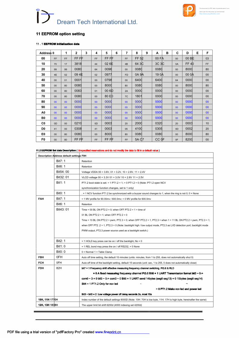
11 EEPROM option setting 11 EEPROM option setting
11 . 1 EEPROM Initialization data11 . 1 EEPROM Initialization data11 . 1 EEPROM Initialization data11 . 1 EEPROM Initialization data11 . 1 EEPROM Initialization data
Address 0 1 2 3 4 5 6 7 8 9 A B C D E F
00 FF FF FF FF FF FF FF FF FF 52 00 FA 00 00 BE 03
10 70 17 3818 44 02 6E 4B 64 3C 3C 3C 0A FF 40 FF
20 99 99 0080 64 0096 00 0080 0080 00 8000 80
30 4E 02 09 4E 02 0977 FD 0A 9A 19 0A 00 00 0A 00
40 00 01 0001 00 0798 00 6400 6400 64 0000 00
50 00 80 0080 00 8000 80 0080 0080 00 8000 80
60 00 80 0083 01 00 6D 2A 0000 0000 00 0000 00
70 00 80 0080 00 80 E0 7C 1801 0000 00 0000 00
80 00 00 0000 00 0000 00 0000 0000 00 0000 00
90 00 00 0000 00 0000 00 0000 0000 00 0000 00
A0 00 00 0000 00 0000 00 0000 0000 00 0000 00
B0 00 00 0000 00 0000 00 0000 0000 00 0000 00
C0 0D 00 0210 0D 0003 20 2000 0320 20 0003 10
D0 41 00 0308 41 0003 05 4100 0305 0D 0002 20
E0 00 80 0080 00 8000 80 0080 0080 00 8000 80
F0 00 80 FF FF FF FF FF FF 5A C7 CC 0F 0F 8200 00
11.2 EEPROM Set data Description ( Unspecified reservations and do not modify the data to fill in a default value )11.2 EEPROM Set data Description ( Unspecified reservations and do not modify the data to fill in a default value )11.2 EEPROM Set data Description ( Unspecified reservations and do not modify the data to fill in a default value )11.2 EEPROM Set data Description ( Unspecified reservations and do not modify the data to fill in a default value )
Description Address default settings F9H
Bit7: 1 Retention
Bit6: 1 Retention
Bit54: 00 Voltage VDDA 00 = 3.6V, 01 = 3.2V, 10 = 2.8V, 11 = 2.4V
Bit32: 01 VLCD voltage 00 = 3.3V 01 = 3.0V 10 = 2.8V 11 = 2.5V
Bit1: 1 PT1.2 boot state is set: = 1 PT1.2 = 1; = 0 PT1.2 = 0 (Note: PT1.2 open NCV
synchronization function changes, set to 1 only)
Bit0: 1 . = 1 NCV function PT1.2 be synchronized with a buzzer sound changes to 1, when the ring is not 0; 0 = None
FAH Bit7: 1 = 1 MV profile for 60.00mv / 600.0mv; = 0 MV profile for 600.0mv
Bit6: 1 Retention
Bit43: 01 Time = 00 BL ON PT2.2 = 0; when OFF PT2.2 = 1 = time of
01 BL ON PT2.2 = 1; when OFF PT2.2 = 0
Time = 10 BL ON PT2.2 = pwm, PT2.3 = 0; when OFF PT2.2 = 1, PT2.3 = when 1 = 11 BL ON PT2.2 = pwm, PT2.3 = 1;
when OFF PT2 .2 = 1, PT2.3 = 0 (Note: backlight high / low output mode, PT2.3 as LVD detection port; backlight mode
PWM output, PT2.3 power source used as a backlight switch.)
Bit2: 1 = 1 HOLD key press can be on / off the backlight, No = 0
Bit1: 0 = 1 REL bond may press the on / off RS232, = 0 None
Bit0: 0 0 = Normal 1 = Table Clamp
FBH 0FH Auto off time setting, the default 15 minutes (units: minutes, from 1 to 255, does not automatically shut 0)
FCH 0FH Auto-off time of the backlight setting, default 15 seconds (unit: sec, 1 to 255, 0 does not automatically close)
FDH 82H bit7 = 1 Frequency shift effective measuring frequency channel switching. Pt3.6 & RLD bit7 = 1 Frequency shift effective measuring frequency channel switching. Pt3.6 & RLD bit7 = 1 Frequency shift effective measuring frequency channel switching. Pt3.6 & RLD
~ ~
= 0 A fixed measuring frequency channel Pt3.6 Bit6 = 1 UART Transmission format bit3 ~ 0-> = 0 A fixed measuring frequency channel Pt3.6 Bit6 = 1 UART Transmission format bit3 ~ 0-> = 0 A fixed measuring frequency channel Pt3.6 Bit6 = 1 UART Transmission format bit3 ~ 0-> = 0 A fixed measuring frequency channel Pt3.6 Bit6 = 1 UART Transmission format bit3 ~ 0-> = 0 A fixed measuring frequency channel Pt3.6 Bit6 = 1 UART Transmission format bit3 ~ 0->
com0 ~ 3 = 0 bit3 ~ 0-> com3 ~ 0 Bit5 = 1 UART send 14bytes (seg0 seg13) = 0 15bytes (seg0 seg14) com0 ~ 3 = 0 bit3 ~ 0-> com3 ~ 0 Bit5 = 1 UART send 14bytes (seg0 seg13) = 0 15bytes (seg0 seg14) com0 ~ 3 = 0 bit3 ~ 0-> com3 ~ 0 Bit5 = 1 UART send 14bytes (seg0 seg13) = 0 15bytes (seg0 seg14)
Bit4 = 1 PT1.2 Only for ncv led Bit4 = 1 PT1.2 Only for ncv led Bit4 = 1 PT1.2 Only for ncv led
= 0 PT1.2 Make ncv led and power led = 0 PT1.2 Make ncv led and power led = 0 PT1.2 Make ncv led and power led = 0 PT1.2 Make ncv led and power led = 0 PT1.2 Make ncv led and power led
Bit3 ~ bit0 = 2 Low voltage power off delay seconds 2s, most 15s Bit3 ~ bit0 = 2 Low voltage power off delay seconds 2s, most 15s Bit3 ~ bit0 = 2 Low voltage power off delay seconds 2s, most 15s Bit3 ~ bit0 = 2 Low voltage power off delay seconds 2s, most 15s Bit3 ~ bit0 = 2 Low voltage power off delay seconds 2s, most 15s
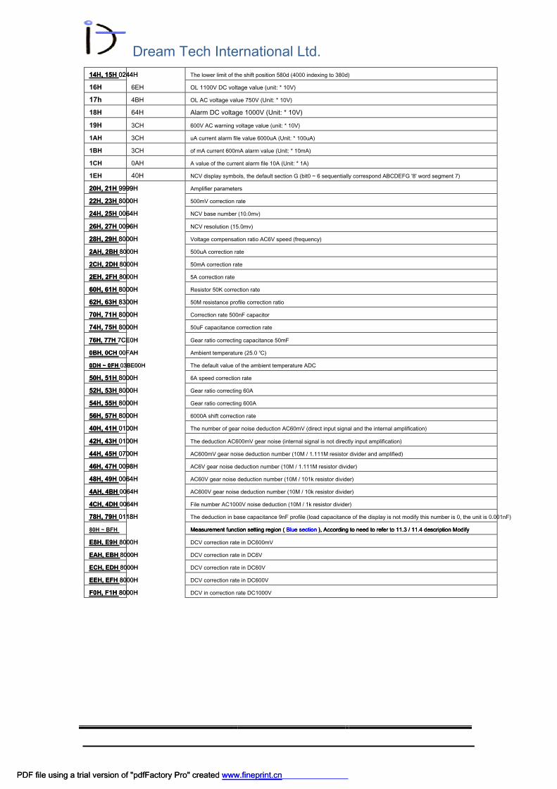
10H, 11H 1770H 10H, 11H 1770H Index number of the default settings 6000D (Note: 10H: 70H is low byte, 11H: 17H is high byte, hereinafter the same)
12H, 13H 1838H 12H, 13H 1838H The upper limit bit shift 6200d (4000 indexing set 4200d)
PDF file using a trial version of "pdfFactory Pro" created www.fineprint.cnPDF file using a trial version of "pdfFactory Pro" created www.fineprint.cn
This document is a PDF editor to generate speed, if you
want to get rid of the prompt, go and download:
http://www.jisupdfeditor.com/
Dream Tech International Ltd.
14H, 15H 0244H 14H, 15H 0244H The lower limit of the shift position 580d (4000 indexing to 380d)
16H 6EH OL 1100V DC voltage value (unit: * 10V)
17h 4BH OL AC voltage value 750V (Unit: * 10V)
18H 64H Alarm DC voltage 1000V (Unit: * 10V)
19H 3CH 600V AC warning voltage value (unit: * 10V)
1AH 3CH uA current alarm file value 6000uA (Unit: * 100uA)
1BH 3CH of mA current 600mA alarm value (Unit: * 10mA)
1CH 0AH A value of the current alarm file 10A (Unit: * 1A)
1EH 40H NCV display symbols, the default section G (bit0 ~ 6 sequentially correspond ABCDEFG '8' word segment 7)
20H, 21H 9999H 20H, 21H 9999H Amplifier parameters
22H, 23H 8000H 22H, 23H 8000H 500mV correction rate
24H, 25H 0064H 24H, 25H 0064H NCV base number (10.0mv)
26H, 27H 0096H 26H, 27H 0096H NCV resolution (15.0mv)
28H, 29H 8000H 28H, 29H 8000H Voltage compensation ratio AC6V speed (frequency)
2AH, 2BH 8000H 2AH, 2BH 8000H 500uA correction rate
2CH, 2DH 8000H 2CH, 2DH 8000H 50mA correction rate
2EH, 2FH 8000H 2EH, 2FH 8000H 5A correction rate
60H, 61H 8000H 60H, 61H 8000H Resistor 50K correction rate
62H, 63H 8300H 62H, 63H 8300H 50M resistance profile correction ratio
70H, 71H 8000H 70H, 71H 8000H Correction rate 500nF capacitor
74H, 75H 8000H 74H, 75H 8000H 50uF capacitance correction rate
76H, 77H 7CE0H 76H, 77H 7CE0H Gear ratio correcting capacitance 50mF
0BH, 0CH 00FAH 0BH, 0CH 00FAH Ambient temperature (25.0 ℃)
0DH ~ 0FH 03BE00H 0DH ~ 0FH 03BE00H The default value of the ambient temperature ADC
50H, 51H 8000H 50H, 51H 8000H 6A speed correction rate
52H, 53H 8000H 52H, 53H 8000H Gear ratio correcting 60A
54H, 55H 8000H 54H, 55H 8000H Gear ratio correcting 600A
56H, 57H 8000H 56H, 57H 8000H 6000A shift correction rate
40H, 41H 0100H 40H, 41H 0100H The number of gear noise deduction AC60mV (direct input signal and the internal amplification)
42H, 43H 0100H 42H, 43H 0100H The deduction AC600mV gear noise (internal signal is not directly input amplification)
44H, 45H 0700H 44H, 45H 0700H AC600mV gear noise deduction number (10M / 1.111M resistor divider and amplified)
46H, 47H 0098H 46H, 47H 0098H AC6V gear noise deduction number (10M / 1.111M resistor divider)
48H, 49H 0064H 48H, 49H 0064H AC60V gear noise deduction number (10M / 101k resistor divider)
4AH, 4BH 0064H 4AH, 4BH 0064H AC600V gear noise deduction number (10M / 10k resistor divider)
4CH, 4DH 0064H 4CH, 4DH 0064H File number AC1000V noise deduction (10M / 1k resistor divider)
78H, 79H 0118H 78H, 79H 0118H The deduction in base capacitance 9nF profile (load capacitance of the display is not modify this number is 0, the unit is 0.001nF)
80H ~ BFH Measurement function setting region ( Blue section ), According to need to refer to 11.3 / 11.4 description Modify Measurement function setting region ( Blue section ), According to need to refer to 11.3 / 11.4 description Modify Measurement function setting region ( Blue section ), According to need to refer to 11.3 / 11.4 description Modify
E8H, E9H 8000H E8H, E9H 8000H DCV correction rate in DC600mV
EAH, EBH 8000H EAH, EBH 8000H DCV correction rate in DC6V
ECH, EDH 8000H ECH, EDH 8000H DCV correction rate in DC60V
EEH, EFH 8000H EEH, EFH 8000H DCV correction rate in DC600V
F0H, F1H 8000H F0H, F1H 8000H DCV in correction rate DC1000V
PDF file using a trial version of "pdfFactory Pro" created www.fineprint.cnPDF file using a trial version of "pdfFactory Pro" created www.fineprint.cn
Dream Tech International Ltd.
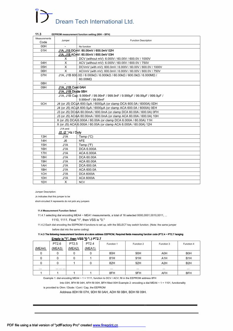
11.3 EEPROM measurement function setting (80H ~ BFH)
Measurements
Code
Jumper Function Description
00H - No function
01H J1A, J1B DCmV: 60.00mV / 600.0mV 02H J1A, J1B DCmV: 60.00mV / 600.0mV 02H
J1A, J1B ACmV: 60.00mV / 600.0mV 03H J1A, J1B ACmV: 60.00mV / 600.0mV 03H
X DCV (without mV): 6.000V / 60.00V / 600.0V / 1000V
04H X ACV (without mV): 6.000V / 60.00V / 600.0V / 750V
05H X DCVmV (with mV): 600.0mV / 6.000V / 60.00V / 600.0V / 1000V
06H X ACVmV (with mV): 600.0mV / 6.000V / 60.00V / 600.0V / 750V
07H J1A, J1B 600.0Ω / 6.000kΩ / 6.000kΩ / 60.00kΩ / 600.0kΩ / 6.000MΩ /
60.00MΩ
08H - -
09H J1A, J1B Cont 0AH J1A, J1B Cont 0AH
J1A, J1B Diode 0BH J1A, J1B Diode 0BH
J1A, J1B Cap: 9.999nF / 99.99nF / 999.9nF / 9.999μF / 99.99μF / 999.9μF /
9.999mF / 99.99mF
0CH J4 (or J5) DCuA 600.0μA / 6000μA (or clamp DCA 600.0A / 6000A) 0DH
J4 (or J5) ACuA 600.0μA / 6000μA (or clamp ACA 600.0A / 6000A) 0EH
J3 (or J5) DCmA 60.00mA / 600.0mA (or clamp DCA 60.00A / 600.0A) 0FH
J3 (or J5) ACmA 60.00mA / 600.0mA (or clamp ACA 60.00A / 600.0A) 10H
X (or J5) DCA 6.000A / 60.00A (or clamp DCA 6.000A / 60.00A) 11H
X (or J5) ACA 6.000A / 60.00A (or clamp ACA 6.000A / 60.00A) 12H
J1A and
J2, j2 ' Hz / Duty J2, j2 ' Hz / Duty
13H J1A Temp (℃)
14H J6 hFE
15H J1A Temp (℉)
16H J1A DCA 6.000A
17H J1A ACA 6.000A
18H J1A DCA 60.00A
19H J1A ACA 60.00A
1AH J1A DCA 600.0A
1BH J1A ACA 600.0A
1CH J1A DCA 6000A
1DH J1A ACA 6000A
1EH X NCV
Jumper Description:
Jx indicates that this jumper to be
short-circuited X represents do not pick any jumpers
11.4 Measurement Function Select
11.4.1 selecting dial encoding MEA4 ~ MEA1 measurements, a total of 16 selected 0000,0001,0010,0011, ...
1110, 1111. Float "1", then VSS is "0."
11.4.2 Each dial encoding the EEPROM 4 functions to set up, with the SELECT key switch function. (Note: the same jumper
before dial into the same coding)
11.4.3 The following measurement functions at a store address EEPROM, Required fields measuring function code (PT2.4 ~ PT2.7 hanging 11.4.3 The following measurement functions at a store address EEPROM, Required fields measuring function code (PT2.4 ~ PT2.7 hanging 11.4.3 The following measurement functions at a store address EEPROM, Required fields measuring function code (PT2.4 ~ PT2.7 hanging
Empty is "1", then VSS "0 ";.) PT2.7 Empty is "1", then VSS "0 ";.) PT2.7 Empty is "1", then VSS "0 ";.) PT2.7 Empty is "1", then VSS "0 ";.) PT2.7
(MEA4)
PT2.6
(MEA3)
PT2.5
(MEA2)
PT2.4
(MEA1)
Function 1 Function 2 Function 3 Function 4
0 0 0 0 80H 90H A0H B0H
0 0 0 1 81H 91H A1H B1H
0 0 1 0 82H 92H A2H B2H
... ... ... ... ... ... ... ...
1 1 1 1 8FH 9FH AFH BFH
Example 1: dial encoding MEA4 ~ 1 = 1111, function to DCV / ACV; fill in the EEPROM address 8FH
Into 03H, 9FH fill 04H, AFH fill 00H, BFH filled 00H Example 2: encoding a dial MEA4 ~ 1 = 1101, functionality
is provided to Ohm / Diode / Cont / Cap, the EEPROM
Address 8DH fill 07H, 9DH fill 0AH, ADH fill 0BH, BDH fill 09H.
PDF file using a trial version of "pdfFactory Pro" created www.fineprint.cnPDF file using a trial version of "pdfFactory Pro" created www.fineprint.cn
Dream Tech International Ltd.
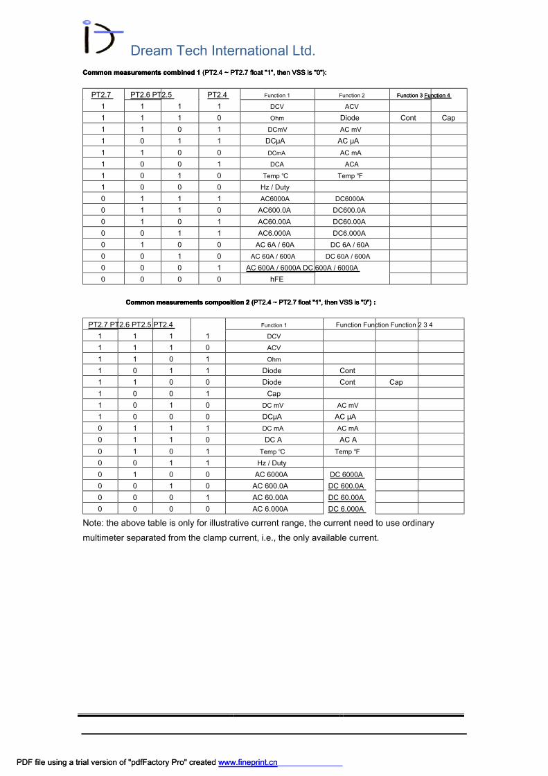
Common measurements combined 1 (PT2.4 ~ PT2.7 float "1", then VSS is "0"): Common measurements combined 1 (PT2.4 ~ PT2.7 float "1", then VSS is "0"): Common measurements combined 1 (PT2.4 ~ PT2.7 float "1", then VSS is "0"): Common measurements combined 1 (PT2.4 ~ PT2.7 float "1", then VSS is "0"):
PT2.7 PT2.6 PT2.5 PT2.4 Function 1 Function 2 Function 3 Function 4 Function 3 Function 4
1 1 1 1 DCV ACV
1 1 1 0 Ohm Diode Cont Cap
1 1 0 1 DCmV AC mV
1 0 1 1 DCμA AC μA
1 1 0 0 DCmA AC mA
1 0 0 1 DCA ACA
1 0 1 0 Temp ℃ Temp ℉
1 0 0 0 Hz / Duty
0 1 1 1 AC6000A DC6000A
0 1 1 0 AC600.0A DC600.0A
0 1 0 1 AC60.00A DC60.00A
0 0 1 1 AC6.000A DC6.000A
0 1 0 0 AC 6A / 60A DC 6A / 60A
0 0 1 0 AC 60A / 600A DC 60A / 600A
0 0 0 1 AC 600A / 6000A DC 600A / 6000A
0 0 0 0 hFE
Common measurements composition 2 (PT2.4 ~ PT2.7 float "1", then VSS is "0") : Common measurements composition 2 (PT2.4 ~ PT2.7 float "1", then VSS is "0") : Common measurements composition 2 (PT2.4 ~ PT2.7 float "1", then VSS is "0") : Common measurements composition 2 (PT2.4 ~ PT2.7 float "1", then VSS is "0") : Common measurements composition 2 (PT2.4 ~ PT2.7 float "1", then VSS is "0") :
PT2.7 PT2.6 PT2.5 PT2.4 Function 1 Function Function Function 2 3 4
1 1 1 1 DCV
1 1 1 0 ACV
1 1 0 1 Ohm
1 0 1 1 Diode Cont
1 1 0 0 Diode Cont Cap
1 0 0 1 Cap
1 0 1 0 DC mV AC mV
1 0 0 0 DCμA AC μA
0 1 1 1 DC mA AC mA
0 1 1 0 DC A AC A
0 1 0 1 Temp ℃ Temp ℉
0 0 1 1 Hz / Duty
0 1 0 0 AC 6000A DC 6000A
0 0 1 0 AC 600.0A DC 600.0A
0 0 0 1 AC 60.00A DC 60.00A
0 0 0 0 AC 6.000A DC 6.000A
Note: the above table is only for illustrative current range, the current need to use ordinary
multimeter separated from the clamp current, i.e., the only available current.
PDF file using a trial version of "pdfFactory Pro" created www.fineprint.cnPDF file using a trial version of "pdfFactory Pro" created www.fineprint.cn
Dream Tech International Ltd.
The method of correcting process 12
The following describes a flow of the calibration circuit of FIG subject to this specification. (See the circuit
diagram). Button assignments during calibration:
SELECT: Skip / function selection SELECT: Skip / function selection
HOLD: Less(-)
Remaining keys: plus (+)
12.1 Calibration mode is entered
J8 short boot into calibration mode. (Resistance profile measurement function should be placed, and remove the input pen)
12.1.1 After checking automatically displayed CAL IC internal circuit, LCD display ADC code value, if there is an error prompting Err0 ~ 4, this time off 12.1.1 After checking automatically displayed CAL IC internal circuit, LCD display ADC code value, if there is an error prompting Err0 ~ 4, this time off
the measurement view dividing resistor is connected for a short circuit, open circuit, the size of the resistance is correct, checked and after the error, and then
reboot, start the calibration process, the self-test parameters are automatically saved to E2 is completed, the buzzer BEEP beep prompts to complete. If too
has been detected, press the SELECT button to skip the examination.
12.1.2 Then automatically check the internal amplifier-related parameters, the parameters are automatically saved to the E2 self-test is completed, the 12.1.2 Then automatically check the internal amplifier-related parameters, the parameters are automatically saved to the E2 self-test is completed, the
buzzer sounds for instructions to complete BEEP. If too has been detected, press the SELECT button to skip the examination.
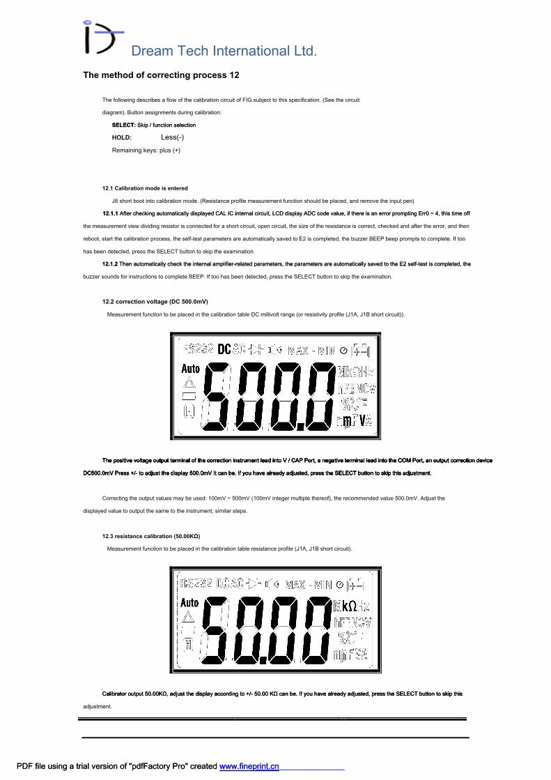
12.2 correction voltage (DC 500.0mV)
Measurement function to be placed in the calibration table DC millivolt range (or resistivity profile (J1A, J1B short circuit)).
The positive voltage output terminal of the correction instrument lead into V / CAP Port, a negative terminal lead into the COM Port, an output correction deviceThe positive voltage output terminal of the correction instrument lead into V / CAP Port, a negative terminal lead into the COM Port, an output correction deviceThe positive voltage output terminal of the correction instrument lead into V / CAP Port, a negative terminal lead into the COM Port, an output correction deviceThe positive voltage output terminal of the correction instrument lead into V / CAP Port, a negative terminal lead into the COM Port, an output correction deviceThe positive voltage output terminal of the correction instrument lead into V / CAP Port, a negative terminal lead into the COM Port, an output correction device
DC500.0mV Press +/- to adjust the display 500.0mV It can be. If you have already adjusted, press the SELECT button to skip this adjustment.DC500.0mV Press +/- to adjust the display 500.0mV It can be. If you have already adjusted, press the SELECT button to skip this adjustment.DC500.0mV Press +/- to adjust the display 500.0mV It can be. If you have already adjusted, press the SELECT button to skip this adjustment.DC500.0mV Press +/- to adjust the display 500.0mV It can be. If you have already adjusted, press the SELECT button to skip this adjustment.
Correcting the output values may be used: 100mV ~ 500mV (100mV integer multiple thereof), the recommended value 500.0mV. Adjust the
displayed value to output the same to the instrument, similar steps.
12.3 resistance calibration (50.00KΩ)
Measurement function to be placed in the calibration table resistance profile (J1A, J1B short circuit).
Calibrator output 50.00KΩ, adjust the display according to +/- 50.00 KΩ can be. If you have already adjusted, press the SELECT button to skip this Calibrator output 50.00KΩ, adjust the display according to +/- 50.00 KΩ can be. If you have already adjusted, press the SELECT button to skip this Calibrator output 50.00KΩ, adjust the display according to +/- 50.00 KΩ can be. If you have already adjusted, press the SELECT button to skip this
adjustment.
PDF file using a trial version of "pdfFactory Pro" created www.fineprint.cnPDF file using a trial version of "pdfFactory Pro" created www.fineprint.cn
Dream Tech International Ltd.
Correcting the output values may be used: 10KΩ ~ 50KΩ (10KΩ integer multiple thereof), the recommended value 50.00KΩ.
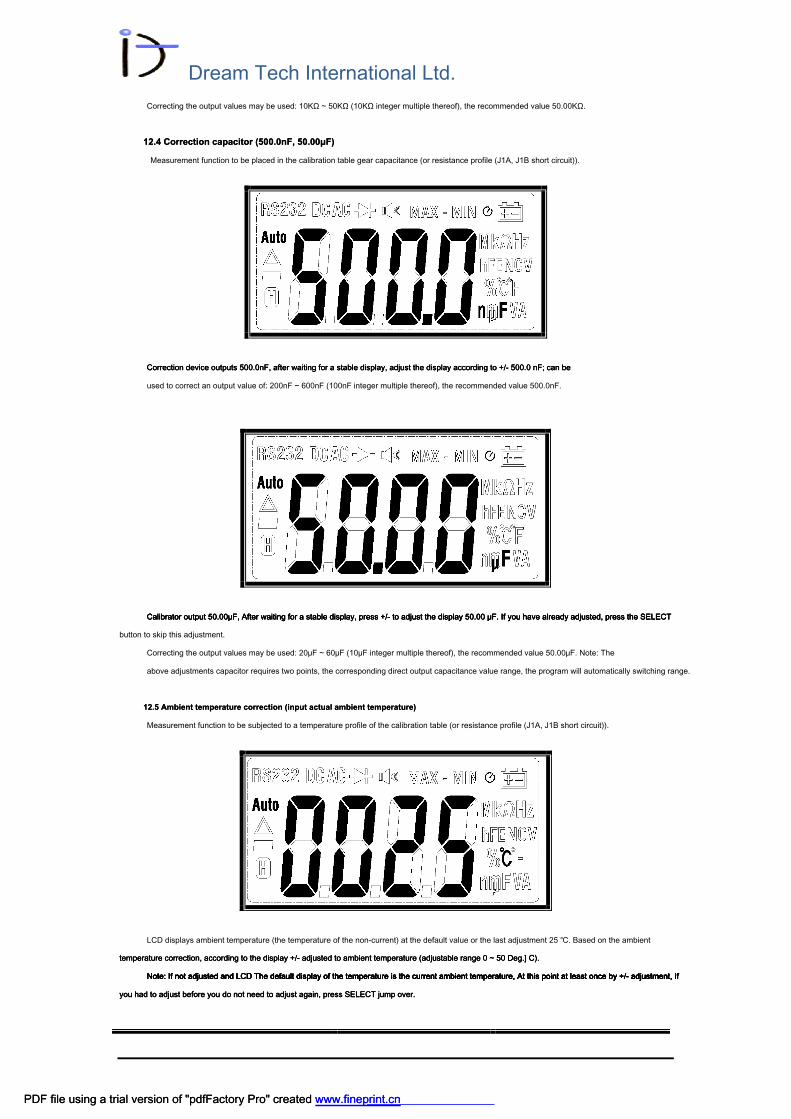
12.4 Correction capacitor (500.0nF, 50.00μF) 12.4 Correction capacitor (500.0nF, 50.00μF)
Measurement function to be placed in the calibration table gear capacitance (or resistance profile (J1A, J1B short circuit)).
Correction device outputs 500.0nF, after waiting for a stable display, adjust the display according to +/- 500.0 nF; can be Correction device outputs 500.0nF, after waiting for a stable display, adjust the display according to +/- 500.0 nF; can be Correction device outputs 500.0nF, after waiting for a stable display, adjust the display according to +/- 500.0 nF; can be
used to correct an output value of: 200nF ~ 600nF (100nF integer multiple thereof), the recommended value 500.0nF.
Calibrator output 50.00μF, After waiting for a stable display, press +/- to adjust the display 50.00 μF. If you have already adjusted, press the SELECT Calibrator output 50.00μF, After waiting for a stable display, press +/- to adjust the display 50.00 μF. If you have already adjusted, press the SELECT Calibrator output 50.00μF, After waiting for a stable display, press +/- to adjust the display 50.00 μF. If you have already adjusted, press the SELECT Calibrator output 50.00μF, After waiting for a stable display, press +/- to adjust the display 50.00 μF. If you have already adjusted, press the SELECT
button to skip this adjustment.
Correcting the output values may be used: 20μF ~ 60μF (10μF integer multiple thereof), the recommended value 50.00μF. Note: The
above adjustments capacitor requires two points, the corresponding direct output capacitance value range, the program will automatically switching range.
12.5 Ambient temperature correction (input actual ambient temperature)12.5 Ambient temperature correction (input actual ambient temperature)
Measurement function to be subjected to a temperature profile of the calibration table (or resistance profile (J1A, J1B short circuit)).
LCD displays ambient temperature (the temperature of the non-current) at the default value or the last adjustment 25 ℃. Based on the ambient
temperature correction, according to the display +/- adjusted to ambient temperature (adjustable range 0 ~ 50 Deg.] C).temperature correction, according to the display +/- adjusted to ambient temperature (adjustable range 0 ~ 50 Deg.] C).temperature correction, according to the display +/- adjusted to ambient temperature (adjustable range 0 ~ 50 Deg.] C).
Note: If not adjusted and LCD The default display of the temperature is the current ambient temperature, At this point at least once by +/- adjustment, If Note: If not adjusted and LCD The default display of the temperature is the current ambient temperature, At this point at least once by +/- adjustment, If Note: If not adjusted and LCD The default display of the temperature is the current ambient temperature, At this point at least once by +/- adjustment, If Note: If not adjusted and LCD The default display of the temperature is the current ambient temperature, At this point at least once by +/- adjustment, If Note: If not adjusted and LCD The default display of the temperature is the current ambient temperature, At this point at least once by +/- adjustment, If Note: If not adjusted and LCD The default display of the temperature is the current ambient temperature, At this point at least once by +/- adjustment, If
you had to adjust before you do not need to adjust again, press SELECT jump over.you had to adjust before you do not need to adjust again, press SELECT jump over.you had to adjust before you do not need to adjust again, press SELECT jump over.
PDF file using a trial version of "pdfFactory Pro" created www.fineprint.cnPDF file using a trial version of "pdfFactory Pro" created www.fineprint.cn
Dream Tech International Ltd.
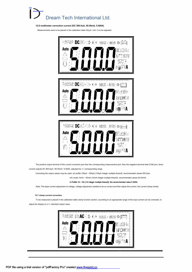
12.6 multimeter correction current (DC 500.0uA, 50.00mA, 5.000A)
Measurements were to be placed in the calibration table DCμA / mA / A to be adjusted.
The positive output terminal of the current correctors pen then the corresponding measurement port, then the negative terminal lead COM port, direct
current outputs DC 500.0μA / 50.00mA / 5.000A, adjusted by +/- corresponding range.
Correcting the output values may be used: uA profile 100μA ~ 500μA (100μA integer multiple thereof), recommended values 500.0μA;
mA mode 10mA ~ 50mA (10mA integer multiple thereof), recommended values 50.00mA;
A Profile 1A ~ 5A (1A integer multiple thereof), the recommended value 5.000A.A Profile 1A ~ 5A (1A integer multiple thereof), the recommended value 5.000A.
Note: The base current adjustment of voltage, voltage adjustment needed to be so correct and then adjust the current, the current clamp similar.
12.7 clamp current correction
To be measured is placed in the calibration table clamp function section, according to an appropriate range of the input current can be corrected, to
adjust the display to a +/- standard output value.
PDF file using a trial version of "pdfFactory Pro" created www.fineprint.cnPDF file using a trial version of "pdfFactory Pro" created www.fineprint.cn

Dream Tech International Ltd.
60HZ AC output signal recommended adjustment, output correction value of each range as follows:
6.000A: 1A ~ 5A (1A integer multiple thereof), the recommended value 5.000A;
6.000A / 60.00A, 60.00A / 600.0A, 60.00A, 600.0A: 10A ~ 50A (10A integer multiple thereof), recommended values 50.00A;
600.0A / 6000A, 6000A: 100A ~ 500A (100A integer multiple thereof), the recommended value 500.0A; Note: 1 can separate automatic shift range
when corrected to a small-scale, low current output corrected easily. The correction profile 6000A automatically shift between the measured values 600.0A
/ 6000A, this time to adjust the output current of 500.0A, 6.000A and if speed is automatically switched between 600.0mA / 6.000A, 5.000 direct output A
current is adjusted.
2. Meter output current should be corrected before the full-scale signal of about 600mV (corresponding to 6000count),
Do not too much deviation, the signal is too large can cause overflow signal is too small may result in insufficient resolution.
Correction voltage range 12.8
Measurement function to be placed in the calibration table DC voltage profile, if the range is set to: DC600Mv / 6V / 60V / 600V / 1000V, calibration
input signal is recommended: DC500mv / 5v / 50v / 500v / 1000v, appropriate parameters may also be provided on their own calibration, to adjust the
display to a +/- standard output value to the calibration current range.
Note:
Step 1. Power On Self Test (12.1) After completion, can go directly to adjust the function, if the dial unmodified coding
When varying (PT2.7 ~ 2.4), press Select key, you can ignore the current adjustments, go to the next adjustment. The default voltage adjustments 12.2, 12.3
resistors, capacitors 12.4, 12.5 four ambient temperature, and can be done without having to switch dial adjustment converted to the corresponding function
in the default function of the resistance profile.
2. When the adjustment process, standard input signal, to wait for the display stabilizes before Press +/- adjustment. Avoid exceeding output
Allowing the signal value range.
3. The error will affect the voltage regulator adjustment current readjusted if the voltage, the current also needs readjustment. 4. Correction function is
set in the process does not shift, a signal short circuit, open circuit or jitters will cause an error or adjustment error becomes large. If adjustment data over the
allowable error (+/- 80%), and the highest digit LCD display or show greater than 6 +/- key press operation will not respond to "OL", no buzzer sound. Normal
operation and calibration data is written right after E2 buzzer BEEP beep, data may alter normal but no buzzer sound indicates that the data is not stored
properly, readjust again. If the check is still valid E2 line, and J8 jumper is shorted.
5. Please do not adjust the data other than the recommended value.
6. After calibration is complete, determines J8 jumper has been disconnected, normally after power test.
PDF file using a trial version of "pdfFactory Pro" created www.fineprint.cnPDF file using a trial version of "pdfFactory Pro" created www.fineprint.cn
Dream Tech International Ltd.
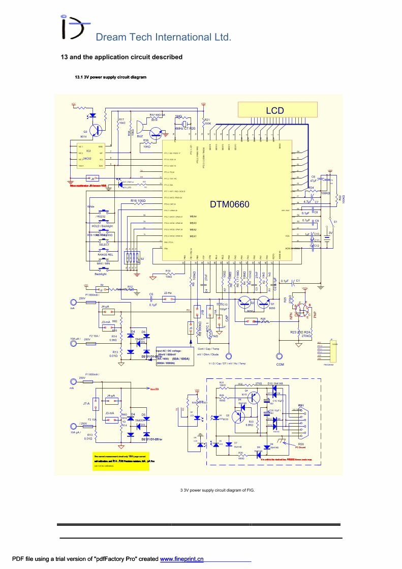
13 and the application circuit described
13.1 3V power supply circuit diagram 13.1 3V power supply circuit diagram
3 3V power supply circuit diagram of FIG.
1kΩ
V / Ω / Cap / DT / mV / Hz / Temp
COM
C12 1μF
C90.1μF
C10 1μF
C11 1μF
C6
47μF
4MHz CT R20
1MΩ
LCD
C74.7μf
C8
0.1μF
Q2
8050
Q1
8050
VDD
C5
0.1μF
VDD
HOLD / Backlight
RANGE REL
/ RS232
Hz / Duty
SELECT
NC 1
NC 2
NC 3
VSS 4
VDD
8
WP
7
SCL
6
SDA
5
IC2
24C02
3V
MAX / MIN
R19 10kΩ R18 200Ω
White
R10
10kΩ
C10.1μF
R16 100Ω
J2-Hz
mV / Ohm / Diode
S1
J8
When recalibration J8 Connect VSS .When recalibration J8 Connect VSS .When recalibration J8 Connect VSS .When recalibration J8 Connect VSS .When recalibration J8 Connect VSS .
R26
100KΩ J6 hFE
E
J5
(60A / 600A)
CE
E
VDDA
E
Cont / Cap / Temp
B
R23 20Ω R24
270kΩ
60mV / 600mV
B
S2
C
Input AC / DC voltage:
1a
2a
(6A / 60A)
3a
(600A / 6000A)
4a
R17
10kΩ
R21
100K
VCC
Backlight
ACM 49 VDDA
50
VSS
54
VGG
51
CA
52
CB
53
VPP / RST
55
VDD
56
VLCD
57
COM0
58
COM1
59
COM2
60
COM3
61
SEG0
62
SEG1
63
SEG2
64
PT1.7 / BZ / PSDO 17
PT1.6 / SCK 18
PT1.5 / SDO 19
PT1.4 / TX 20
PT1.3 / TST / RC
21
PT1.2 / SDI
22
PT1.1 / INT1 / PSD / SCE 23
PT1.0 / INTO / PSCK 24
PT3.6 / CNT 25
PT3.7 / CPMO 26
PT2.7 / INT27 / CPM3 27
PT2.6 / INT26 / CPM2 28
PT2.5 / INT25 / CPM1 29
PT2.4 / INT24 / CPM0 30
PB5 / PT3.5
31
PB4
32
DTM0660
MEA4
MEA3
MEA2
MEA1
Q3
9014
R14
0.99Ω
R15
99Ω
R13
0.01Ω
10A μA /
mA
F1 800mA /
250V
F2 10A /
250V
D4
D2 D1 D1-D5 forD2 D1 D1-D5 for
1N4001
D5
D3
J3-mA
J4-μA
R14
1Ω
R15
99Ω
R13
0.01Ω
10A μA /
mA
F1 800mA /
250V
F2 10A
/ 250V
D4
D2 D1 D1-D5 forD2 D1 D1-D5 for
1N4001
D5
D3
J3-mA
J4-μA
J7-A
Meet R9Meet R9
The current measurement circuit only 10A Large current The current measurement circuit only 10A Large current The current measurement circuit only 10A Large current
self-calibration, and R14 , R15 Precision resistors, mA , μA You self-calibration, and R14 , R15 Precision resistors, mA , μA You self-calibration, and R14 , R15 Precision resistors, mA , μA You self-calibration, and R14 , R15 Precision resistors, mA , μA You self-calibration, and R14 , R15 Precision resistors, mA , μA You self-calibration, and R14 , R15 Precision resistors, mA , μA You self-calibration, and R14 , R15 Precision resistors, mA , μA You self-calibration, and R14 , R15 Precision resistors, mA , μA You self-calibration, and R14 , R15 Precision resistors, mA , μA You
can not be calibrated.
R9
123456
J9
PROGRAM
RST
PT1.0
PT1.1
PT1.7
VDD
VSS
TX
RX
R32 270Ω
R33
6.8KΩ
R31
10KΩ
R29
500Ω
Q4
9015
C15 10μF /
16V
Q5
9015
D6
1N4148
D7
1N4148 D8
1N4148
D9
1N4148
R30
500Ω
R28
500Ω R8 500Ω
162 738 495
RS1
RS9
D10 1N4148
D11 1N4148
D12 1N4148
D13
1N4148
VDD
It is within the dashed box RS232 Annex route map.It is within the dashed box RS232 Annex route map.It is within the dashed box RS232 Annex route map.
PC GroundPC Ground
C20 10μF /
16V
DE
LED
DE
LED DR
LED
DR
LED
C13
100pF *
R34
100KΩ
EXT_PWR or
NCV_LED
R35
100
R12
1MΩ R36 1MΩ
VDD Hz
J2 '
J7
BUZ
R37 50Ω Q4
9014
R38
10KΩ
C14
104
PDF file using a trial version of "pdfFactory Pro" created www.fineprint.cnPDF file using a trial version of "pdfFactory Pro" created www.fineprint.cn
C3
27
nF
PT
C 1
R8 900kΩ
R7
10
0Ω
R1
1kΩ
R2
10
kΩ
R3
1
01
kΩ
R4
1
0M
Ω
R5
1
.1
11
MΩ
R6
10M
Ω
R9
100kΩ
C2 0.1μF
R2
2
10
0K
Ω
C4
2
7n
F
J1
A
NP
N
R2
5
27
0kΩ
PN
P
1a
2a
3a
4a
1b
2b
3b
4b
PB
3
33
PB
1 / P
B2 34
PB
0
35
FT
P
36
FT
N
37
RLU
38
RLD
39
PA
6
40
PA
5
41
PA
4
42
PA
3
43
PA
2
44
PA
1
45
PA
0
46
RE
FO
47
AG
ND
48
SE
G3
1
SE
G4
2
SE
G5
3
SE
G6
4
SE
G7
5
SE
G8
6
SE
G9
7
SE
G10
8
SE
G11
9
SE
G12
10
SE
G13
11
SE
G14
12
PT
2.3 / LV
DIN
/ T
MC
KI
13
PT
2.2 / P
WM
/ P
FD
14
PT
2.1 / X
TI
15
PT
2.0
16
RX
TX
R36
10kΩ
J1
B
CA
P
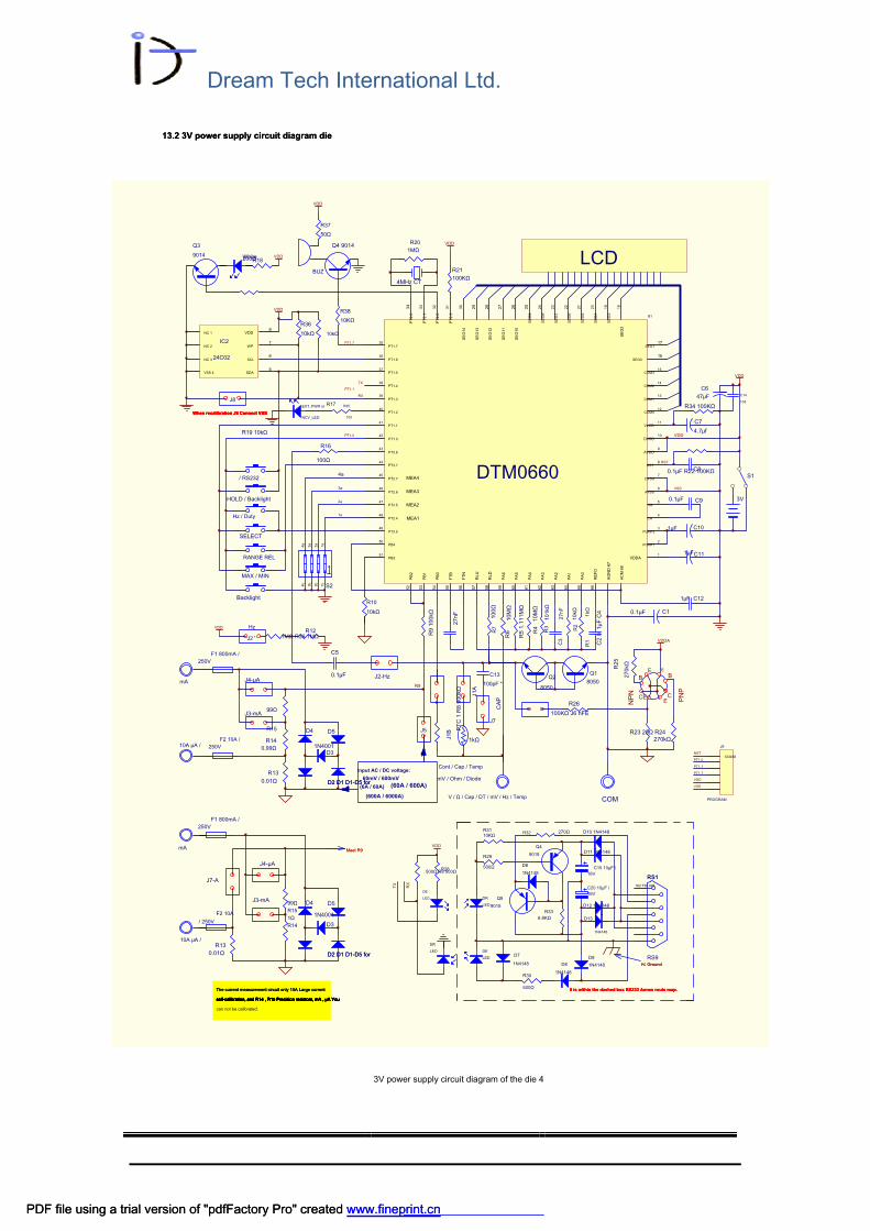
Dream Tech International Ltd.
13.2 3V power supply circuit diagram die 13.2 3V power supply circuit diagram die
3V power supply circuit diagram of the die 4
R14
0.99Ω
R15
99Ω
R13
0.01Ω
10A μA /
mA
V / Ω / Cap / DT / mV / Hz / Temp
COM
C12 1μF
C90.1μF
C10 1μF
C11 1μF
C6
47μF
4MHz CT
R20
1MΩ
LCD
C7
4.7μf
C8
0.1μF R22 100KΩ
Q2
8050
Q1
8050
VDD
C5
0.1μF
VDD
HOLD / Backlight
RANGE REL
/ RS232
Hz / Duty
SELECT
F1 800mA /
250V
F2 10A /
250V
D4
D2 D1 D1-D5 forD2 D1 D1-D5 for
1N4001
D5
D3
BUZ
NC 1
NC 2
NC 3
VSS 4
VDD
8
WP
7
SCL
6
SDA
5
IC2
24C02
3V
MAX / MIN
R19 10kΩ
R18 200Ω White
R10
10kΩ C10.1μF
R16
100Ω
J2-Hz
J3-mA
S1
J8
When recalibration J8 Connect VSSWhen recalibration J8 Connect VSSWhen recalibration J8 Connect VSSWhen recalibration J8 Connect VSS
R26
100KΩ J6 hFE
E
J5
(60A / 600A)
CE
E
VDDA
E
Cont / Cap / Temp
B
R23 20Ω R24
270kΩ
60mV / 600mV
B
S2
C
J4-μA
Input AC / DC voltage:
1a
2a
(6A / 60A)
3a
(600A / 6000A)
4a
R17
10kΩ
R21
100KΩ
R14
1Ω
R15
99Ω
R13
0.01Ω
10A μA /
mA
F1 800mA /
250V
F2 10A
/ 250V
D4
D2 D1 D1-D5 forD2 D1 D1-D5 for
1N4001
D5
D3
J3-mA
J4-μA
J7-A
Meet R9Meet R9
The current measurement circuit only 10A Large current The current measurement circuit only 10A Large current The current measurement circuit only 10A Large current
self-calibration, and R14 , R15 Precision resistors, mA , μA You self-calibration, and R14 , R15 Precision resistors, mA , μA You self-calibration, and R14 , R15 Precision resistors, mA , μA You self-calibration, and R14 , R15 Precision resistors, mA , μA You self-calibration, and R14 , R15 Precision resistors, mA , μA You self-calibration, and R14 , R15 Precision resistors, mA , μA You self-calibration, and R14 , R15 Precision resistors, mA , μA You self-calibration, and R14 , R15 Precision resistors, mA , μA You self-calibration, and R14 , R15 Precision resistors, mA , μA You
can not be calibrated.
R9
VDD
Backlight
VDDA
1
PUMP1
2
PUMP2
3
CA
4
CB
5
AVSS
6
DVSS
7
RST
8
AVDD
9
DVDD
10
VLCD
11
COM0
12
COM1
13
COM2
14
COM3
15
SEG1
17
SEG0
16
PT1.2
40
PT1.7
35
PT1.6
36
PT1.5
37
PT1.4
38
PT1.3
39
PT1.1
41
PT1.0
42
PT3.5
49
PT3.6
43
PT3.7
44
PT2.7
45
PT2.6
46
PT2.5
47
PT2.4
48
PB4
50
PB3
51
R?
DTM0660
Q3
9014
MEA1
MEA2
MEA3
MEA4
123456
J9
PROGRAM
RST
PT1.0
PT1.1
PT1.7
VDD
VSS
PT1.0
PT1.1
PT1.7
RST
VDD
VSS
TX
RX
VDD
R32 270Ω
R33
6.8KΩ
R31
10KΩ
R29
500Ω
Q4
9015
C15 10μF /
16V
Q5
9015
D6
1N4148
D7
1N4148 D8
1N4148
D9
1N4148
R30
500Ω
R28
500Ω R8 500Ω
162 738 495
RS1
RS9
D10 1N4148
D11 1N4148
D12 1N4148
D13
1N4148
VDD
It is within the dashed box RS232 Annex route map.It is within the dashed box RS232 Annex route map.It is within the dashed box RS232 Annex route map.
PC GroundPC Ground
C20 10μF /
16V
DE
LED
DE
LED DR
LED
DR
LED
R34 100KΩEXT_PWR or
NCV_LED
R35
100
R12
1MΩ R36 1MΩ
VDD Hz
J2 '
R36
10kΩ
R37
50Ω
VDD
Q4 9014
R38
10KΩ
1kΩ
mV / Ohm / Diode
C13
100pF *
J7
C14
104
PDF file using a trial version of "pdfFactory Pro" created www.fineprint.cnPDF file using a trial version of "pdfFactory Pro" created www.fineprint.cn
C3
27nF
R7
100Ω
R1
1kΩ
R2
10
kΩ
R3
101kΩ
R4
10M
Ω
R5 1.111M
Ω
R6
10M
Ω
R9 100kΩ
C2 0. 1μF
C
4
27nF
NP
N
R2
5
27
0kΩ
PN
P
1a
2a
3a
4a
1b
2b
3b
4b
PB
2
52
PB
1
53
PB
0
54
FT
B
55
FT
N
56
RL
U
57
RL
D
58
PA
6
59
PA
5
60
PA
4
61
PA
3
62
PA
2
63
PA
1
64
PA
0
65
RE
FO
66
AG
ND
6
7
AC
M 6
8
SE
G2
18
SE
G3
19
SE
G4
20
SE
G5
21
SE
G6
22
SE
G7
23
SE
G8
24
SE
G9
25
SE
G1
0
26
SE
G1
1
27
SE
G1
2
28
SE
G1
3
29
SE
G1
4
30
PT
2.3
31
PT
2.2
32
PT
2.1
33
PT
2.0
34
RX
TX
PT
C 1 R
8 900kΩ
J1B
J1A
CA
P
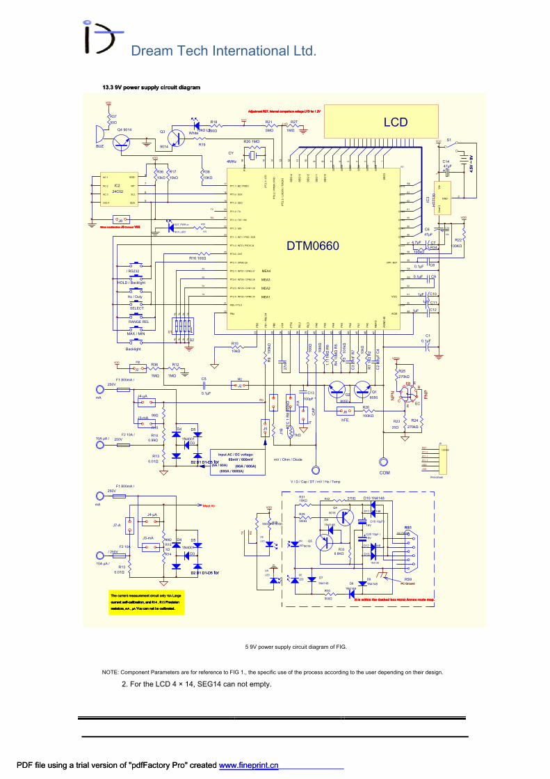
Dream Tech International Ltd.
13.3 9V power supply circuit diagram 13.3 9V power supply circuit diagram
5 9V power supply circuit diagram of FIG.
NOTE: Component Parameters are for reference to FIG 1., the specific use of the process according to the user depending on their design.
2. For the LCD 4 × 14, SEG14 can not empty.
V / Ω / Cap / DT / mV / Hz / Temp
COM
C12 1μF
C90.1μF
C10 1μF
C11 1μF
C6
47μF
4MHz
CY
R20 1MΩ
LCD
C74.7μF
C8
0.1μF
R22
100KΩ
Q2
8050
Q1
8050
VCC
C5
0.1μF
VDD
HOLD / Backlight
RANGE REL
/ RS232
Hz / Duty
SELECT
NC 1
NC 2
NC 3
VSS 4
VDD
8
WP
7
SCL
6
SDA
5
IC2
24C02
GND
2
C14
47μF
MAX / MIN
R21
5MΩ
R27
1MΩ
R18
200Ω
R19
10kΩ LS
White
R10
10kΩ
C1
0.1μF
R16 100Ω
Hz
J2
01
S1
J8
When recalibration J8 Connect VSSWhen recalibration J8 Connect VSSWhen recalibration J8 Connect VSSWhen recalibration J8 Connect VSS
EB
E
E
EC
R25
270kΩ
R23
20Ω
R26
100KΩ
R24
270kΩ
VDDA
J6
hFE
C
B
S2
1a
2a
3a
4a
R17
10kΩ
R12
1MΩ
Adjustment R27, Internal comparison voltage LVD for 1.2VAdjustment R27, Internal comparison voltage LVD for 1.2VAdjustment R27, Internal comparison voltage LVD for 1.2VAdjustment R27, Internal comparison voltage LVD for 1.2VAdjustment R27, Internal comparison voltage LVD for 1.2VAdjustment R27, Internal comparison voltage LVD for 1.2V
VCC
VDD
Backlight
J5
(60A / 600A)
60mV / 600mV
Input AC / DC voltage:
(6A / 60A)
(600A / 6000A)
ACM
49
VDDA
50
VSS
54
VGG
51
CA
52
CB
53
VPP / RST
55
VDD
56
VLCD
57
COM0
58
COM1
59
COM2
60
COM3
61
SEG0
62
SEG1
63
SEG2
64
PT1.7 / BZ / PSDO
17
PT1.6 / SCK
18
PT1.5 / SDO
19
PT1.4 / TX
20
PT1.3 / TST / RC
21
PT1.2 / SDI
22
PT1.1 / INT1 / PSD / SCE
23
PT1.0 / INTO / PSCK 24
PT3.6 / CNT
25
PT3.7 / CPMO 26
PT2.7 / INT27 / CPM3 27
PT2.6 / INT26 / CPM2 28
PT2.5 / INT25 / CPM1 29
PT2.4 / INT24 / CPM0 30
PB5 / PT3.5
31
PB4
32
R?
DTM0660
MEA4
MEA3
MEA2
MEA1
Q3
9014
R14
0.99Ω
R15
99Ω
R13
0.01Ω
10A μA /
mA
F1 800mA /
250V
F2 10A /
250V
D4
D2 D1 D1-D5 forD2 D1 D1-D5 for
1N4001
D5
D3
J3-mA
J4-μA
R14
1Ω
R15
99Ω
R13
0.01Ω
10A μA /
mA
F1 800mA /
250V
F2 10A
/ 250V
D4
D2 D1 D1-D5 forD2 D1 D1-D5 for
1N4001
D5
D3
J3-mA
J4-μA
J7-A
Meet R9Meet R9
The current measurement circuit only 10A Large The current measurement circuit only 10A Large The current measurement circuit only 10A Large
current self-calibration, and R14 , R15 Precision current self-calibration, and R14 , R15 Precision current self-calibration, and R14 , R15 Precision current self-calibration, and R14 , R15 Precision current self-calibration, and R14 , R15 Precision
resistors, mA , μA You can not be calibrated.resistors, mA , μA You can not be calibrated.resistors, mA , μA You can not be calibrated.resistors, mA , μA You can not be calibrated.resistors, mA , μA You can not be calibrated.
R9
123456
J9
PROGRAM
RST
PT1.0
PT1.1
PT1.7
VDD
VSS
TX
RX
R32 270Ω
R33
6.8KΩ
R31
10KΩ
R29
500Ω
Q4
9015
C15 10μF /
16V
Q5
9015
D6
1N4148
D7
1N4148 D8
1N4148
D9
1N4148
R30
500Ω
R28
500Ω R8 500Ω
162 738 495
RS1
RS9
D10 1N4148
D11 1N4148
D12 1N4148
D13
1N4148
VDD
It is within the dashed box RS232 Annex route map.It is within the dashed box RS232 Annex route map.It is within the dashed box RS232 Annex route map.
PC GroundPC Ground
C20 10μF /
16V
DE
LED
DE
LED DR
LED
DR
LED
EXT_PWR or
NCV_LED
R35
100
R34
100kΩ
R36
1MΩ
VDD Hz
J2 '
LVD
1kΩ
mV / Ohm / Diode
C13
100pF *
J7
R36
10kΩ
BUZ
R37
50Ω
VDD
Q4 9014
R38
10KΩ
C14
104
PDF file using a trial version of "pdfFactory Pro" created www.fineprint.cnPDF file using a trial version of "pdfFactory Pro" created www.fineprint.cn
C3 27nF
R
7
100Ω
R1 1kΩ
R
2
10kΩ
R3
101kΩ
R4 10M
Ω R
5
1.111M
Ω R
6
10M
Ω
R9
100kΩ
C2 0.1μF
C
4
27nF
Vin
1
Vo
ut 3
IC
3
HT
7130
4.5V ~
9V
4.5V ~
9V
4.5V ~
9V
NP
N
PN
P
1a
2a
3a
4a
1b
2b
3b
4b
PB
3
33
PB
1 / P
B2
3
4
PB
0
35
FT
P
36
FT
N
37
RL
U
38
RL
D
39
PA
6
40
PA
5
41
PA
4
42
PA
3
43
PA
2
44
PA
1
45
PA
0
46
RE
FO
47
AG
ND
4
8
SE
G3
1
SE
G4
2
SE
G5
3
SE
G6
4
SE
G7
5
SE
G8
6
SE
G9
7
SE
G1
0
8
SE
G1
1
9
SE
G1
2
10
SE
G1
3
11
SE
G1
4
12
PT
2.3 / LV
DIN
/ T
MC
KI
13
PT
2.2
/ P
WM
/ P
FD
14
PT
2.1 / X
TI
15
PT
2.0
16
RX
TX
PT
C 1 R
8 900kΩ
J1B
J1A
CA
P
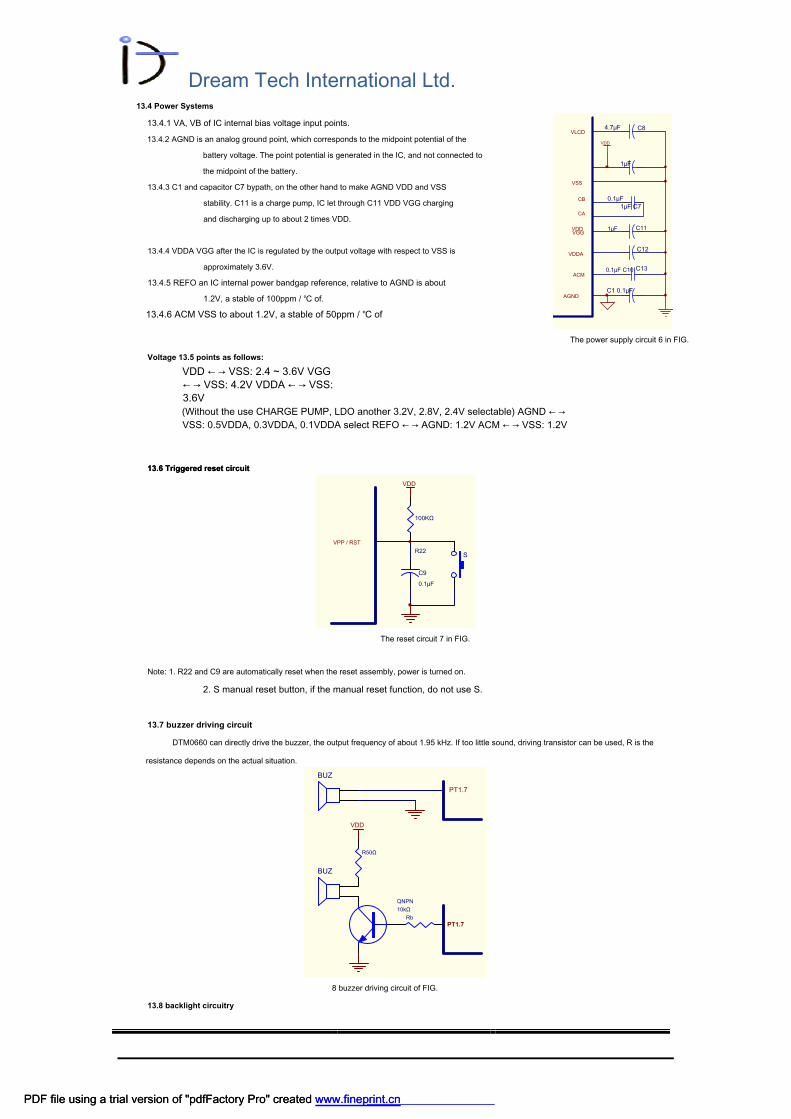
Dream Tech International Ltd.
13.4 Power Systems
13.4.1 VA, VB of IC internal bias voltage input points.
13.4.2 AGND is an analog ground point, which corresponds to the midpoint potential of the
battery voltage. The point potential is generated in the IC, and not connected to
the midpoint of the battery.
13.4.3 C1 and capacitor C7 bypath, on the other hand to make AGND VDD and VSS
stability. C11 is a charge pump, IC let through C11 VDD VGG charging
and discharging up to about 2 times VDD.
13.4.4 VDDA VGG after the IC is regulated by the output voltage with respect to VSS is
approximately 3.6V.
13.4.5 REFO an IC internal power bandgap reference, relative to AGND is about
1.2V, a stable of 100ppm / ℃ of.
13.4.6 ACM VSS to about 1.2V, a stable of 50ppm / ℃ of
C130.1μF C10
0.1μF
C11 1μF
C12
1μF C7
1μF
C84.7μF
C1 0.1μF
VLCD
CB
CA
VGG
VDDA
ACM
VDD
VSS
AGND
VDD
The power supply circuit 6 in FIG.
Voltage 13.5 points as follows:
VDD ← → VSS: 2.4 ~ 3.6V VGG
← → VSS: 4.2V VDDA ← → VSS:
3.6V
(Without the use CHARGE PUMP, LDO another 3.2V, 2.8V, 2.4V selectable) AGND ← →
VSS: 0.5VDDA, 0.3VDDA, 0.1VDDA select REFO ← → AGND: 1.2V ACM ← → VSS: 1.2V
13.6 Triggered reset circuit13.6 Triggered reset circuit
VPP / RST
C9
0.1μF
R22
100KΩ
VDD
S
The reset circuit 7 in FIG.
Note: 1. R22 and C9 are automatically reset when the reset assembly, power is turned on.
2. S manual reset button, if the manual reset function, do not use S.
13.7 buzzer driving circuit
DTM0660 can directly drive the buzzer, the output frequency of about 1.95 kHz. If too little sound, driving transistor can be used, R is the
resistance depends on the actual situation.
BUZ
PT1.7
BUZ
R50Ω
Rb
10kΩ
QNPN
VDD
PT1.7
8 buzzer driving circuit of FIG.
13.8 backlight circuitry
PDF file using a trial version of "pdfFactory Pro" created www.fineprint.cnPDF file using a trial version of "pdfFactory Pro" created www.fineprint.cn
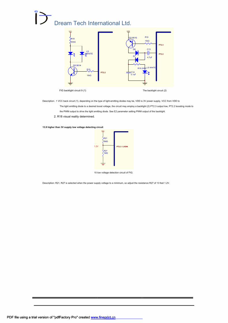
Dream Tech International Ltd.
R19
10kΩ
VCC
PT2.2
Q3 9015
D6
D7
LS WHITE
R18 200Ω
C13
4.7uF
C14
0.1uF
R19
10kΩ
VDD
PT2.2
PT2.3
Q3 9014
LS
WHITE
R18
200Ω
FIG backlight circuit 9 (1) The backlight circuit (2)
Description:. 1 VCC back circuit (1), depending on the type of light-emitting diodes may be, VDD is 3V power supply, VCC from VDD to
The light emitting diode to a desired boost voltage, the circuit may employ a backlight (2) PT2.3 output low, PT2.2 boosting mode to
the PWM output to drive the light emitting diode. See E2 parameter setting PWM output of the backlight.
2. R18 visual reality determined.
13.9 higher than 3V supply low voltage detecting circuit
R27
1MΩ
VCC
PT2.3 / LVDIN
R21
5MΩ
1.2V
10 low voltage detection circuit of FIG.
Description: R21, R27 is selected when the power supply voltage to a minimum, so adjust the resistance R27 of 13 feet 1.2V.
PDF file using a trial version of "pdfFactory Pro" created www.fineprint.cnPDF file using a trial version of "pdfFactory Pro" created www.fineprint.cn
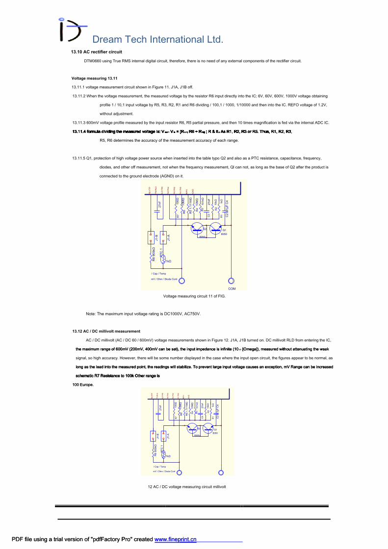
Dream Tech International Ltd.
13.10 AC rectifier circuit
DTM0660 using True RMS internal digital circuit, therefore, there is no need of any external components of the rectifier circuit.
Voltage measuring 13.11
13.11.1 voltage measurement circuit shown in Figure 11. J1A, J1B off.
13.11.2 When the voltage measurement, the measured voltage by the resistor R6 input directly into the IC; 6V, 60V, 600V, 1000V voltage obtaining
profile 1 / 10,1 input voltage by R5, R3, R2, R1 and R6 dividing / 100,1 / 1000, 1/10000 and then into the IC. REFO voltage of 1.2V,
without adjustment.
13.11.3 600mV voltage profile measured by the input resistor R6, R5 partial pressure, and then 10 times magnification is fed via the internal ADC IC.
13.11.4 formula dividing the measured voltage is: V out = V in × [R s / ( R6 + R S)] ; R & lt s As R1, R2, R3 or R5. Thus, R1, R2, R3, 13.11.4 formula dividing the measured voltage is: V out = V in × [R s / ( R6 + R S)] ; R & lt s As R1, R2, R3 or R5. Thus, R1, R2, R3, 13.11.4 formula dividing the measured voltage is: V out = V in × [R s / ( R6 + R S)] ; R & lt s As R1, R2, R3 or R5. Thus, R1, R2, R3, 13.11.4 formula dividing the measured voltage is: V out = V in × [R s / ( R6 + R S)] ; R & lt s As R1, R2, R3 or R5. Thus, R1, R2, R3, 13.11.4 formula dividing the measured voltage is: V out = V in × [R s / ( R6 + R S)] ; R & lt s As R1, R2, R3 or R5. Thus, R1, R2, R3, 13.11.4 formula dividing the measured voltage is: V out = V in × [R s / ( R6 + R S)] ; R & lt s As R1, R2, R3 or R5. Thus, R1, R2, R3, 13.11.4 formula dividing the measured voltage is: V out = V in × [R s / ( R6 + R S)] ; R & lt s As R1, R2, R3 or R5. Thus, R1, R2, R3, 13.11.4 formula dividing the measured voltage is: V out = V in × [R s / ( R6 + R S)] ; R & lt s As R1, R2, R3 or R5. Thus, R1, R2, R3, 13.11.4 formula dividing the measured voltage is: V out = V in × [R s / ( R6 + R S)] ; R & lt s As R1, R2, R3 or R5. Thus, R1, R2, R3, 13.11.4 formula dividing the measured voltage is: V out = V in × [R s / ( R6 + R S)] ; R & lt s As R1, R2, R3 or R5. Thus, R1, R2, R3, 13.11.4 formula dividing the measured voltage is: V out = V in × [R s / ( R6 + R S)] ; R & lt s As R1, R2, R3 or R5. Thus, R1, R2, R3,
R5, R6 determines the accuracy of the measurement accuracy of each range.
13.11.5 Q1, protection of high voltage power source when inserted into the table typo Q2 and also as a PTC resistance, capacitance, frequency,
diodes, and other off measurement, not when the frequency measurement, Ql can not, as long as the base of Q2 after the product is
connected to the ground electrode (AGND) on it.
1kΩ
COM
Q2
8050
Q1
8050
mV / Ohm / Diode Cont
/ Cap / Temp
Voltage measuring circuit 11 of FIG.
Note: The maximum input voltage rating is DC1000V, AC750V.
13.12 AC / DC millivolt measurement
AC / DC millivolt (AC / DC 60 / 600mV) voltage measurements shown in Figure 12. J1A, J1B turned on. DC millivolt RLD from entering the IC,
the maximum range of 600mV (200mV, 400mV can be set), the input impedance is infinite (10 11 [Omega]), measured without attenuating the weak the maximum range of 600mV (200mV, 400mV can be set), the input impedance is infinite (10 11 [Omega]), measured without attenuating the weak the maximum range of 600mV (200mV, 400mV can be set), the input impedance is infinite (10 11 [Omega]), measured without attenuating the weak
signal, so high accuracy. However, there will be some number displayed in the case where the input open circuit, the figures appear to be normal, as
long as the lead into the measured point, the readings will stabilize. To prevent large input voltage causes an exception, mV Range can be increased long as the lead into the measured point, the readings will stabilize. To prevent large input voltage causes an exception, mV Range can be increased long as the lead into the measured point, the readings will stabilize. To prevent large input voltage causes an exception, mV Range can be increased
schematic R7 Resistance to 100k Other range isschematic R7 Resistance to 100k Other range isschematic R7 Resistance to 100k Other range isschematic R7 Resistance to 100k Other range isschematic R7 Resistance to 100k Other range is
100 Europe. 100 Europe.
12 AC / DC voltage measuring circuit millivolt
1kΩ
Q2
8050
Q1
8050
mV / Ohm / Diode Cont
/ Cap / Temp
PDF file using a trial version of "pdfFactory Pro" created www.fineprint.cnPDF file using a trial version of "pdfFactory Pro" created www.fineprint.cn
C3
2
7n
F
PT
C 1
R8 900kΩ
R7
1
00
Ω
R1
1kΩ
R2
10
kΩ
R3
101kΩ
R4
10
MΩ
R5
1
.1
11
MΩ
R6
10M
Ω
C2
0
.1
μF
C
4
27
nF
J1
-B
J1-A
PB
0 F
TP
FT
N R
LU
RLD
P
A6
PA
5 P
A4
PA
3 P
A2
PA
1 P
A0
RE
FO
AG
ND
C3
27nF
PT
C 1
R8 900kΩ
R7
100Ω
R1
1kΩ
R2
1
0kΩ
R3
1
01
kΩ
R4
10M
Ω
R5 1.111M
Ω
R6
10M
Ω
C2
0
.1
μF
C
4
27nF
J1-B
J1-A
PB
0 F
TP
FT
N R
LU
RL
D P
A6
PA
5 P
A4
PA
3 P
A2
PA
1 P
A0
RE
FO
AG
ND
Dream Tech International Ltd.
Current measuring 13.13
13.13.1 μA profile sampling resistance is R13 + R14 + R15, mA is the profile sampling resistor R14 + R15,10A sampling resistance profile is R15. Were
measured by switching the mode switch, when the measured uA, J3 is turned off, the closing J4; when measuring mA, disconnect J4,
J3 close; when measuring the bulk current gear 10A, J3, J4 OFF .
13.13.2 μA, mA third gear 10A, and the voltage drop generated up to 0.6V and 0.1V. These voltages are fed to the comparator compares the voltage, if
more than 60mV, the voltage signal directly into the A / D converter; if less than 60mV, the internal electronic switch is closed, a 10x
magnification and then into the A / D converter.
13.13.3 method for measuring current in FIG 13, the self-calibration method can be corrected μA, mA and 10A stalls, R13, R14 and R15 does not
affect the accuracy of the accuracy of current measurement. It may also be precision resistors R14 and R15, R13 and manual tuning
embodiment to calibrate a large current, i.e., the same as the conventional DMM.
13.13.4 method for measuring current in FIG 14, the self-calibration method can be corrected only file 10A, no manual adjustment R13. Accuracy μA
and mA measured is the precision resistors R14 and R15 to the guaranteed.
R14
0.99Ω
R15
99Ω
R13
0.01Ω
10A μA /
mA
F1
800mA / 250V
F2 10A /
250V
D4
D2 D1 D1-D5 forD2 D1 D1-D5 for
1N4001
D5
D3
J3-mA
J4-μA
Meet R9Meet R9
FIG current measurement circuit 13 (a)
R14
1Ω
R15
99Ω
R13
0.01Ω
10A μA /
mA
F1 800mA /
250V
F2 10A
/ 250V
D4
D2 D1 D1-D5 forD2 D1 D1-D5 for
1N4001
D5
D3
J3-mA
J4-μA
J7-A
Meet R9Meet R9
Current measurement circuit 14 in FIG. (B)
13.14 resistance measurement
Measuring the resistance shown in Figure 15. J1A, J1B turned on.
The resistance is measured as a reference standard resistor, the resistance to be measured with a standard resistance test comparing
measured resistance value is obtained. Profile for the standard resistance 60MΩ 10MΩ (R6), of other modes are standard resistors R4, R5, R3, R2, R1,
measuring the resistance, a voltage of 1.0V IC internal (with respect to AGND), respectively, by the voltage resistors R1, R2, R3, R4, R5 outputted
through R7, PTC resistor under test to generate a current I, this current flows through the resistor to produce a measured voltage VR, the voltage IC
and the voltage by the return R8 standard resistance compared calculating the resistance of the measured resistance. (60 M [Omega voltage output
gear directly to the test by the resistor R6)
When resistance measurement J1A, J1B to be turned. Filter capacitor C3 is a reference resistor, C4 is a filter capacitor of the measured resistance.
Resistance measurement circuit 15 in FIG.
1kΩ
COM
Q2
8050
Q1
8050
mV / Ohm / Diode Cont
/ Cap / Temp
PDF file using a trial version of "pdfFactory Pro" created www.fineprint.cnPDF file using a trial version of "pdfFactory Pro" created www.fineprint.cn
C3
27nF
PT
C 1
R8 900kΩ
R7
100Ω
R1
1kΩ
R2
10kΩ
R3
10
1kΩ
R4
10M
Ω
R5 1.111M
Ω
R6
10M
Ω
C2 0. 1μF
C
4
27nF
J1-B
J1-A
PB
0 F
TP
FT
N R
LU
RLD
P
A6
PA
5 P
A4
PA
3 P
A2
PA
1 P
A0
RE
FO
AG
ND
Dream Tech International Ltd.
13.15 diode measurements
Figure 16 diode measurement.
Diode IC 3.2V measurements generated by the internal voltage (relative to AGND), was applied to the diodes through PTC R7 positive output
terminal. Diodes forward voltage drop VD of about 0.5V-0.7V, VD through VD R6 and R5 partial weight of 1/10 into the ADC, the VD value display.
J1A, J1B are mode switch, J1A diode measurement; J1B closed. DTM0660 diode output when the test voltage is measured 3.2V, a detectable
contour LED diode forward conduction. When the detection diode voltage drop exceeds 3.0V, indicating overflow to "OL" tabular. Appears "OL"
reverse diode may be damaged or measurement.
1kΩ
COM
Q2
8050
Q1
8050
mV / Ohm / Diode
Cont / Cap / Temp
3.2V ADC
DX
Diode measurement circuit 16 in FIG.
13.16 Continuity Check
Figure 17 is detected off.
When off internal IC and generates 1.0V voltage (relative to AGND) outputted by R7, applied through PTC-off point to be detected. J1A,
J1B are mode switch, on closing, when the Rx made off detection voltage V Rx By R8 input IC. Seen from FIG., 1.0V * Rx / (R7 + PTC + Rx) = J1B are mode switch, on closing, when the Rx made off detection voltage V Rx By R8 input IC. Seen from FIG., 1.0V * Rx / (R7 + PTC + Rx) = J1B are mode switch, on closing, when the Rx made off detection voltage V Rx By R8 input IC. Seen from FIG., 1.0V * Rx / (R7 + PTC + Rx) =
0.025V
Rx = 0.025 (R7 + PTC) /0.975
Known R7 = 100Ω, if PTC = 1kΩ, the Rx ≒ 28.2Ω, if PTC = 1.5K, the Rx ≒ 41Ω. Thus, when the PTC between 1kΩ ~
1.5kΩ, the buzzer is turned off at point Rx between 28Ω ~ 41Ω.
1kΩ
COM
Q2
8050
Q1
8050
mV / Ohm / Diode Cont
/ Cap / Temp
RX
0.025V CMP
Off detecting circuit 17 of FIG.
PDF file using a trial version of "pdfFactory Pro" created www.fineprint.cnPDF file using a trial version of "pdfFactory Pro" created www.fineprint.cn
PT
C 1
R7 100Ω
J1-A
RL
D
AG
ND
R51.111M
Ω R
6
10M
Ω P
A6
10M
Ω P
A6
PA
5
RL
U
R8 900kΩ
J1-B
PB
0
PT
C 1
R8 900kΩ
R7 100Ω
J1-B
J1-A
PB
0
RL
D
AG
ND
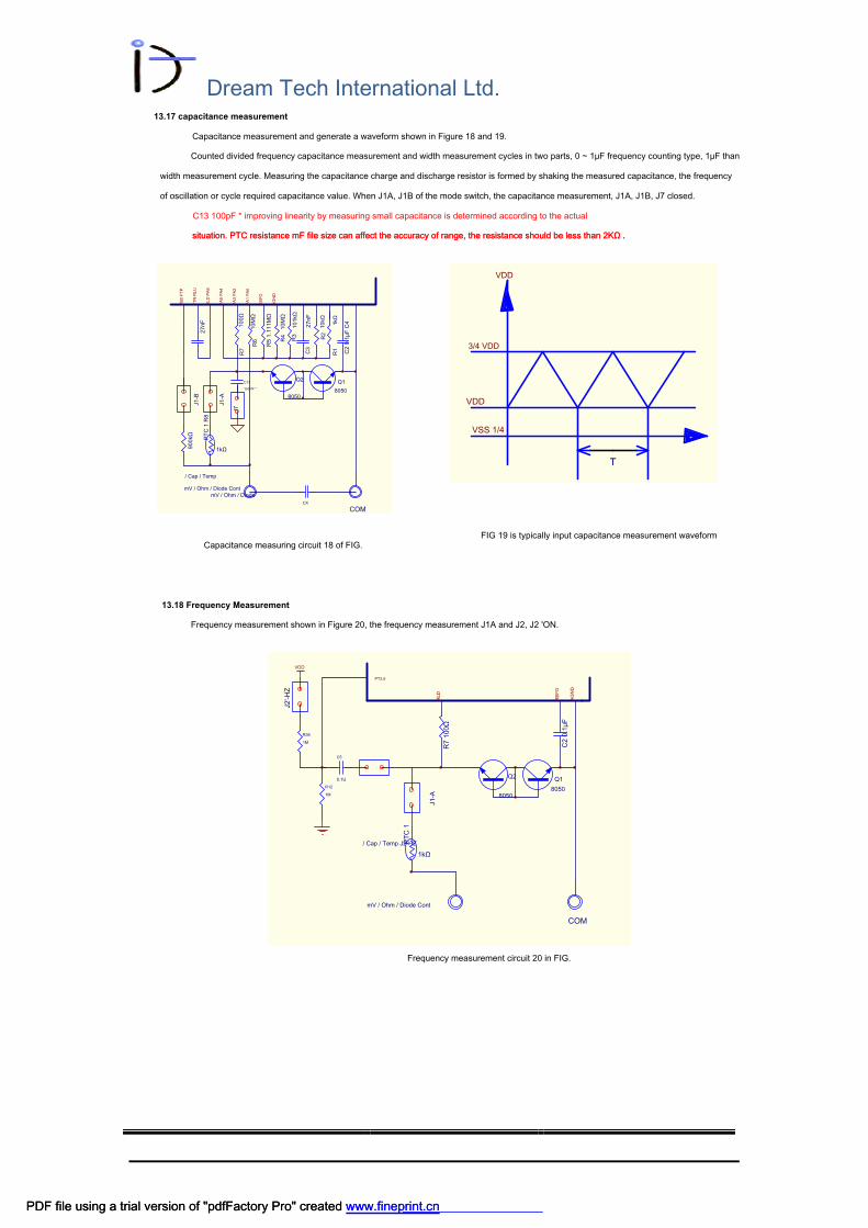
Dream Tech International Ltd.
13.17 capacitance measurement
Capacitance measurement and generate a waveform shown in Figure 18 and 19.
Counted divided frequency capacitance measurement and width measurement cycles in two parts, 0 ~ 1μF frequency counting type, 1μF than
width measurement cycle. Measuring the capacitance charge and discharge resistor is formed by shaking the measured capacitance, the frequency
of oscillation or cycle required capacitance value. When J1A, J1B of the mode switch, the capacitance measurement, J1A, J1B, J7 closed.
C13 100pF * improving linearity by measuring small capacitance is determined according to the actual
situation. PTC resistance mF file size can affect the accuracy of range, the resistance should be less than 2KΩ . situation. PTC resistance mF file size can affect the accuracy of range, the resistance should be less than 2KΩ .
1kΩ
COM
Q2
8050
Q1
8050
mV / Ohm / Diode Cont
/ Cap / Temp
CX
C13
100PF *
mV / Ohm / Diode
Capacitance measuring circuit 18 of FIG.
VSS 1/4
VDD
3/4 VDD
VDD
T
FIG 19 is typically input capacitance measurement waveform
13.18 Frequency Measurement
Frequency measurement shown in Figure 20, the frequency measurement J1A and J2, J2 'ON.
1kΩ
COM
Q2
8050
Q1
8050
mV / Ohm / Diode Cont
/ Cap / Temp J2-HZ
C5
0.1U
R36
1M
R12
1M
VDD
PT3.6
Frequency measurement circuit 20 in FIG.
PDF file using a trial version of "pdfFactory Pro" created www.fineprint.cnPDF file using a trial version of "pdfFactory Pro" created www.fineprint.cn
C3
27nF
PT
C 1 R
8
900kΩ
R7
100Ω
R1
1kΩ
R2
10kΩ
R3
101kΩ
R4
10M
Ω
R5 1.111M
Ω
R6
10M
Ω
C2 0.1μF
C
4
27nF
J1-B
J1-A
PB
0 F
TP
FT
N R
LU
RLD
P
A6
PA
5 P
A4
PA
3 P
A2
PA
1 P
A0
RE
FO
AG
ND
J7
PT
C 1
R7 100Ω
C2 0.1μF
J1-A
RL
D
RE
FO
AG
ND
J2'-H
Z
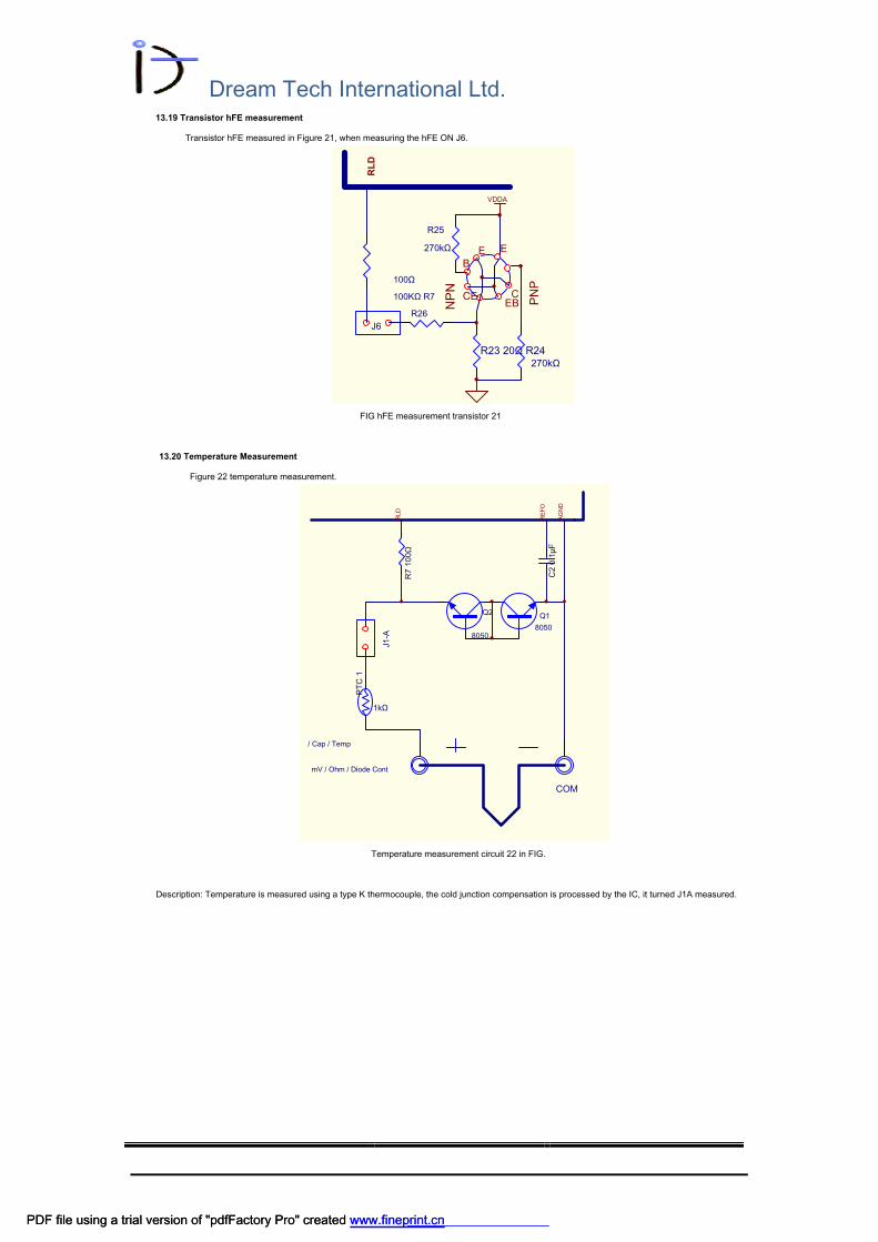
Dream Tech International Ltd.
13.19 Transistor hFE measurement
Transistor hFE measured in Figure 21, when measuring the hFE ON J6.
E
CE
E
VDDA
EB
R25
270kΩ
R23 20Ω R24
270kΩ
B
C
R26
100KΩ R7
100Ω
J6
FIG hFE measurement transistor 21
13.20 Temperature Measurement
Figure 22 temperature measurement.
1kΩ
COM
Q2
8050
Q1
8050
mV / Ohm / Diode Cont
/ Cap / Temp
Temperature measurement circuit 22 in FIG.
Description: Temperature is measured using a type K thermocouple, the cold junction compensation is processed by the IC, it turned J1A measured.
PDF file using a trial version of "pdfFactory Pro" created www.fineprint.cnPDF file using a trial version of "pdfFactory Pro" created www.fineprint.cn
NP
N
PN
P
RL
D
PT
C 1
R7 100Ω
AG
ND
RE
FO
C2 0.1μF
RLD
J1-A
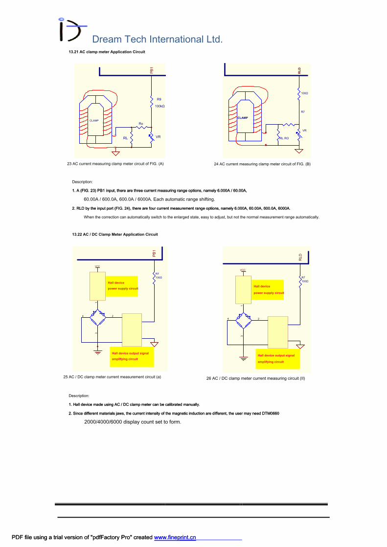
Dream Tech International Ltd.
13.21 AC clamp meter Application Circuit
R9
100kΩ
Ro
RL
CLAMP
VR
23 AC current measuring clamp meter circuit of FIG. (A)
CLAMP
RL RO
VR
R7
100Ω
24 AC current measuring clamp meter circuit of FIG. (B)
Description:
1. A (FIG. 23) PB1 input, there are three current measuring range options, namely 6.000A / 60.00A,1. A (FIG. 23) PB1 input, there are three current measuring range options, namely 6.000A / 60.00A,
60.00A / 600.0A, 600.0A / 6000A. Each automatic range shifting.
2. RLD by the input port (FIG. 24), there are four current measurement range options, namely 6.000A, 60.00A, 600.0A, 6000A.2. RLD by the input port (FIG. 24), there are four current measurement range options, namely 6.000A, 60.00A, 600.0A, 6000A.
When the correction can automatically switch to the enlarged state, easy to adjust, but not the normal measurement range automatically.
13.22 AC / DC Clamp Meter Application Circuit
24
VCC
Hall device
power supply circuit
Hall device output signal
amplifying circuit
R7
100Ω
25 AC / DC clamp meter current measurement circuit (a)
24
VCC
Hall device
power supply circuit
Hall device output signal
amplifying circuit
R7
100Ω
26 AC / DC clamp meter current measuring circuit (II)
Description:
1. Hall device made using AC / DC clamp meter can be calibrated manually. 1. Hall device made using AC / DC clamp meter can be calibrated manually.
2. Since different materials jaws, the current intensity of the magnetic induction are different, the user may need DTM0660 2. Since different materials jaws, the current intensity of the magnetic induction are different, the user may need DTM0660
2000/4000/6000 display count set to form.
PDF file using a trial version of "pdfFactory Pro" created www.fineprint.cnPDF file using a trial version of "pdfFactory Pro" created www.fineprint.cn
PB
1
RL
D
13
PB
1
13
RLD
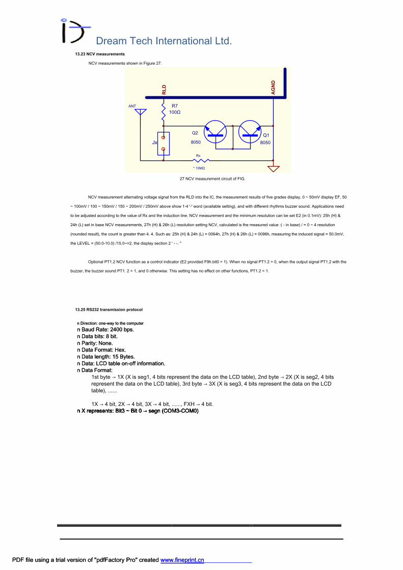
Dream Tech International Ltd.
13.23 NCV measurements
NCV measurements shown in Figure 27.
Q2
8050
Q1
8050
R7
100Ω
Rx
* 10MΩ
ANT
Jx
27 NCV measurement circuit of FIG.
NCV measurement alternating voltage signal from the RLD into the IC, the measurement results of five grades display, 0 ~ 50mV display EF, 50
~ 100mV / 100 ~ 150mV / 150 ~ 200mV / 250mV above show 1-4 '-' word (available setting), and with different rhythms buzzer sound. Applications need
to be adjusted according to the value of Rx and the induction line. NCV measurement and the minimum resolution can be set E2 (in 0.1mV): 25h (H) &
24h (L) set in base NCV measurements, 27h (H) & 26h (L) resolution setting NCV, calculated is the measured value :( - in base) / = 0 ~ 4 resolution
(rounded result), the count is greater than 4. 4. Such as: 25h (H) & 24h (L) = 0064h, 27h (H) & 26h (L) = 0096h, measuring the induced signal = 50.0mV,
the LEVEL = (50.0-10.0) /15.0~=2, the display section 2 ' - -. "
Optional PT1.2 NCV function as a control indicator (E2 provided F9h.bit0 = 1). When no signal PT1.2 = 0, when the output signal PT1.2 with the
buzzer, the buzzer sound PT1. 2 = 1, and 0 otherwise. This setting has no effect on other functions, PT1.2 = 1.
13.25 RS232 transmission protocol
n Direction: one-way to the computer n Direction: one-way to the computer
n Baud Rate: 2400 bps. n Baud Rate: 2400 bps.
n Data bits: 8 bit. n Data bits: 8 bit.
n Parity: None. n Parity: None.
n Data Format: Hex. n Data Format: Hex.
n Data length: 15 Bytes. n Data length: 15 Bytes.
n Data: LCD table on-off information. n Data: LCD table on-off information.
n Data Format: n Data Format:
1st byte → 1X (X is seg1, 4 bits represent the data on the LCD table), 2nd byte → 2X (X is seg2, 4 bits
represent the data on the LCD table), 3rd byte → 3X (X is seg3, 4 bits represent the data on the LCD
table), ......
1X → 4 bit, 2X → 4 bit, 3X → 4 bit, ......, FXH → 4 bit.
n X represents: Bit3 ~ Bit 0 → segn (COM3-COM0) n X represents: Bit3 ~ Bit 0 → segn (COM3-COM0) n X represents: Bit3 ~ Bit 0 → segn (COM3-COM0) n X represents: Bit3 ~ Bit 0 → segn (COM3-COM0)
PDF file using a trial version of "pdfFactory Pro" created www.fineprint.cnPDF file using a trial version of "pdfFactory Pro" created www.fineprint.cn
RL
D
AG
ND

Dream Tech International Ltd.
The liquid crystal display 14
14.1 4 × 15 liquid crystal display structure
MAX - MINRS232
NCV
FIG 28 4 × 15 liquid crystal display structure of FIG.
The liquid crystal display truth table 14.2
29 LCD truth table of FIG.
Note: 1 Operating voltage:. 3V.
2. Drive method: 1/4 Duty, 1/3 Bias.
The liquid crystal display waveform 14.3
The liquid crystal display 30 FIG driving waveform COM
PDF file using a trial version of "pdfFactory Pro" created www.fineprint.cnPDF file using a trial version of "pdfFactory Pro" created www.fineprint.cn
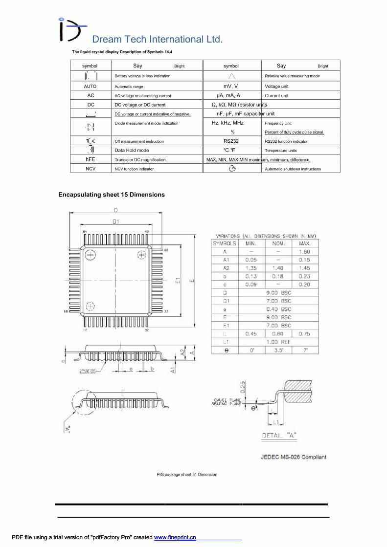
Dream Tech International Ltd.
The liquid crystal display Description of Symbols 14.4
Encapsulating sheet 15 Dimensions
FIG package sheet 31 Dimension
symbol Say Bright symbol Say Bright
Battery voltage is less indication Relative value measuring mode
AUTO Automatic range mV, V Voltage unit
AC AC voltage or alternating current μA, mA, A Current unit
DC DC voltage or DC current Ω, kΩ, MΩ resistor units
DC voltage or current indicative of negative nF, μF, mF capacitor unit
Diode measurement mode indication Hz, kHz, MHz
%
Frequency Unit
Percent of duty cycle pulse signal
Off measurement instruction RS232 RS232 function indicator
Data Hold mode ℃ ℉ Temperature units
hFE Transistor DC magnification MAX, MIN, MAX-MIN maximum, minimum, difference
NCV NCV function indicator Automatic shutdown instructions
PDF file using a trial version of "pdfFactory Pro" created www.fineprint.cnPDF file using a trial version of "pdfFactory Pro" created www.fineprint.cn

Dream Tech International Ltd.
V1.5 Modify recordsV1.5 Modify records
1: eprom Setting content changes ( fdh) = 82h .1: eprom Setting content changes ( fdh) = 82h .1: eprom Setting content changes ( fdh) = 82h .1: eprom Setting content changes ( fdh) = 82h .
2: Buzzer output frequency parameter to 1.95k. V1.6 Modify 2: Buzzer output frequency parameter to 1.95k. V1.6 Modify 2: Buzzer output frequency parameter to 1.95k. V1.6 Modify 2: Buzzer output frequency parameter to 1.95k. V1.6 Modify
records
1 : Change the application circuit. J1 change to J1A, J1B 2: 1 : Change the application circuit. J1 change to J1A, J1B 2: 1 : Change the application circuit. J1 change to J1A, J1B 2: 1 : Change the application circuit. J1 change to J1A, J1B 2: 1 : Change the application circuit. J1 change to J1A, J1B 2:
24C02 WP Feet to 10k Pull-up resistor24C02 WP Feet to 10k Pull-up resistor24C02 WP Feet to 10k Pull-up resistor24C02 WP Feet to 10k Pull-up resistor
V1.7 Modify recordsV1.7 Modify records
1: Increasing the voltage range calibration, changing the eprom set up e8h ~ f1h The default values.1: Increasing the voltage range calibration, changing the eprom set up e8h ~ f1h The default values.1: Increasing the voltage range calibration, changing the eprom set up e8h ~ f1h The default values.1: Increasing the voltage range calibration, changing the eprom set up e8h ~ f1h The default values.1: Increasing the voltage range calibration, changing the eprom set up e8h ~ f1h The default values.1: Increasing the voltage range calibration, changing the eprom set up e8h ~ f1h The default values.
2 : Change the frequency measurement.2 : Change the frequency measurement.
V1.8 Modify recordsV1.8 Modify records
1: ACM Meet PB4, EMC Strengthen immunity test.1: ACM Meet PB4, EMC Strengthen immunity test.1: ACM Meet PB4, EMC Strengthen immunity test.1: ACM Meet PB4, EMC Strengthen immunity test.
2: increase J11 Jumper, as mV Speed input channels.2: increase J11 Jumper, as mV Speed input channels.2: increase J11 Jumper, as mV Speed input channels.2: increase J11 Jumper, as mV Speed input channels.2: increase J11 Jumper, as mV Speed input channels.2: increase J11 Jumper, as mV Speed input channels.
V1.9 Modify recordsV1.9 Modify records
1: cancel mV enter J11 Jumpers can be adjusted depending on the application R7 Resistance, see mV Measuring instructions.1: cancel mV enter J11 Jumpers can be adjusted depending on the application R7 Resistance, see mV Measuring instructions.1: cancel mV enter J11 Jumpers can be adjusted depending on the application R7 Resistance, see mV Measuring instructions.1: cancel mV enter J11 Jumpers can be adjusted depending on the application R7 Resistance, see mV Measuring instructions.1: cancel mV enter J11 Jumpers can be adjusted depending on the application R7 Resistance, see mV Measuring instructions.1: cancel mV enter J11 Jumpers can be adjusted depending on the application R7 Resistance, see mV Measuring instructions.1: cancel mV enter J11 Jumpers can be adjusted depending on the application R7 Resistance, see mV Measuring instructions.1: cancel mV enter J11 Jumpers can be adjusted depending on the application R7 Resistance, see mV Measuring instructions.1: cancel mV enter J11 Jumpers can be adjusted depending on the application R7 Resistance, see mV Measuring instructions.1: cancel mV enter J11 Jumpers can be adjusted depending on the application R7 Resistance, see mV Measuring instructions.
2: VDD End increase 0.1uF Filter capacitor2: VDD End increase 0.1uF Filter capacitor2: VDD End increase 0.1uF Filter capacitor2: VDD End increase 0.1uF Filter capacitor
3: ACM Stabilizing capacitance to the end . 1uF 3: ACM Stabilizing capacitance to the end . 1uF 3: ACM Stabilizing capacitance to the end . 1uF
4: increase UART Upload options4: increase UART Upload options4: increase UART Upload options4: increase UART Upload options
24c02 FDH.6 = 1 selected 9721 Compatible format, FDH.6 = 0 (dtm0660L version)24c02 FDH.6 = 1 selected 9721 Compatible format, FDH.6 = 0 (dtm0660L version)24c02 FDH.6 = 1 selected 9721 Compatible format, FDH.6 = 0 (dtm0660L version)24c02 FDH.6 = 1 selected 9721 Compatible format, FDH.6 = 0 (dtm0660L version)24c02 FDH.6 = 1 selected 9721 Compatible format, FDH.6 = 0 (dtm0660L version)24c02 FDH.6 = 1 selected 9721 Compatible format, FDH.6 = 0 (dtm0660L version)
FDH.5 = 1 send 14Bytes, FDH.5 = 0 send 15Bytes (dtm0660L version)FDH.5 = 1 send 14Bytes, FDH.5 = 0 send 15Bytes (dtm0660L version)FDH.5 = 1 send 14Bytes, FDH.5 = 0 send 15Bytes (dtm0660L version)FDH.5 = 1 send 14Bytes, FDH.5 = 0 send 15Bytes (dtm0660L version)FDH.5 = 1 send 14Bytes, FDH.5 = 0 send 15Bytes (dtm0660L version)FDH.5 = 1 send 14Bytes, FDH.5 = 0 send 15Bytes (dtm0660L version)
5: increase Ncv Indicator Control Options5: increase Ncv Indicator Control Options5: increase Ncv Indicator Control Options5: increase Ncv Indicator Control Options
24c02 FDH.4 = 1 pt1.2 Only ncv led, Active high, other modes is low.24c02 FDH.4 = 1 pt1.2 Only ncv led, Active high, other modes is low.24c02 FDH.4 = 1 pt1.2 Only ncv led, Active high, other modes is low.24c02 FDH.4 = 1 pt1.2 Only ncv led, Active high, other modes is low.
24c02 FDH.4 = 0 pt1.2 As a ncv led And the power indicator.24c02 FDH.4 = 0 pt1.2 As a ncv led And the power indicator.24c02 FDH.4 = 0 pt1.2 As a ncv led And the power indicator.24c02 FDH.4 = 0 pt1.2 As a ncv led And the power indicator.
6 :increase diode / cont Relative value Control Options6 :increase diode / cont Relative value Control Options6 :increase diode / cont Relative value Control Options6 :increase diode / cont Relative value Control Options
24c02 FAH.5 = 0 No relative value function24c02 FAH.5 = 0 No relative value function
24c02 FAH.5 = 1 Relative value function24c02 FAH.5 = 1 Relative value function
PDF file using a trial version of "pdfFactory Pro" created www.fineprint.cnPDF file using a trial version of "pdfFactory Pro" created www.fineprint.cn


![Dream -TVËFMIP:M/CD] Dream Dream Dmam Dream i Honda ... · Dream Dream Dmam Dream i Honda SENSING15ž—— BOX '9/20å - asasM DAIHATSU Mira _- suzuxl AC,Þg 'S suzuKi sp icv-n](https://img.pdfslide.us/doc/110x75/6014ed32110a9c58445c06ba/dream-tvfmipmcd-dream-dream-dmam-dream-i-honda-dream-dream-dmam-dream.jpg)