Embed Size (px)
Citation preview
Solid-State Electronics 65–66 (2011) 45–50
Contents lists available at SciVerse ScienceDirect
Solid-State Electronics
journal homepage: www.elsevier .com/locate /sse
Drain-extended MOS transistors capable for operation at 10 V andat radio frequencies
Andreas Mai ⇑, Holger RückerIHP, Im Technolgiepark 25, 15236 Frankfurt (Oder), Germany
a r t i c l e i n f o
Article history:Available online 24 August 2011
Keywords:MOS devicesLDMOSPower transistorsRadio frequency
0038-1101/$ - see front matter � 2011 Published bydoi:10.1016/j.sse.2011.06.034
⇑ Corresponding author.E-mail address: [email protected] (A
a b s t r a c t
This work reports on the integration of n-type lateral-drain-extended MOS transistors (LDMOS) in a0.13 lm SiGe BiCMOS technology. The transistors are realized with no additional process steps usingthe core dual-gate-oxide CMOS flow only. LDMOS drift regions are formed by compensatinglightly-doped drain (LDD) implantations of NMOS and PMOS transistors of the baseline process. Stableoperation with less than 10% parameter variations in 10 years is achieved up to operating voltages VDD,max
of 10 V for devices with breakdown voltages BVDSS = 30 V and on-resistances RON = 7.3 X mm. Devices fordifferent operating voltages VDD,max are realized by layout variations. Devices with VDD,max = 6 V demon-strate breakdown voltages BVDSS = 25 V, on-resistances RON = 4.9 X mm, and peak transit frequenciesfT = 32 GHz.
� 2011 Published by Elsevier Ltd.
1. Introduction
High-voltage transistors are required in system-on-chip (SoC)technologies for a variety of applications ranging from power man-agement circuits and driver circuits for non-volatile memories orlight-emitting diodes to RF power amplifiers. These demands havebeen addressed in several generations of CMOS and BiCMOS tech-nology platforms by using drain-extended MOS devices [1]. A ma-jor challenge encountered when integrating these devices is therestriction of the number of added process steps to only a few ornone in order to restrict additional costs. Several concepts utilizededicated ion implantation steps for the formation of drift and wellregions of lateral-drain-extended MOS transistors (LDMOS) [2–6].High-voltage devices with no added process steps have beenrealized by using the CMOS well implants for the formation ofthe extended drain regions [7–9]. An alternative concept for theintegration of LDMOS transistors without any additional process-ing effort was proposed in [10]. There, the lightly-doped drain(LDD) implantations of the 3.3 V CMOS transistors were used forthe formation of the drift regions.
Here, we present n-type LDMOS transistors fabricated in adual-gate-oxide 0.13 lm CMOS flow without additional processsteps. The drift regions of the LDMOS transistors are formed by acombination of the LDD implantations of the standard CMOSdevices. In difference to [10], the drift region is divided in two partswith different doping concentrations resulting in reduced on-resistance for devices with the same breakdown voltage. The
Elsevier Ltd.
. Mai).
devices are capable for stable operation up to 10 V with less then10% degradation of any device parameter in 10 years.
2. Design description
The LDMOS devices were integrated in the 0.13 lm SiGe BiC-MOS process of IHP [11]. This process addresses RF and mm-waveapplications with a high level of integration. The technologyoffers high-speed SiGe heterojunction bipolar transistors (fT =240 GHz, fmax = 330 GHz) together with 1.2 V and 3.3 V CMOStransistors, a set of passive RF components, and seven layers ofaluminum interconnects. The integration of LDMOS devicespresented here is independent of the HBT process and uses onlyprocess steps of the core CMOS flow. The CMOS process featurestwo gate oxide thicknesses of 2 nm and 7 nm for 1.2 V and 3.3 VCMOS transistors, respectively.
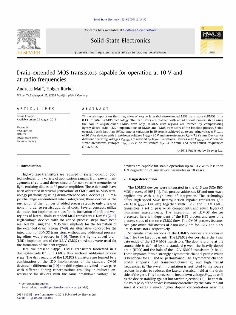
Schematic cross sections of the LDMOS devices are shown inFig. 1 for two layout variants. The LDMOS devices share the 7 nmgate oxide of the 3.3 V MOS transistors. The doping profile at thesource side is defined by the standard p-well, the heavily-dopeddrain (HDD) and the halo of the 1.2 V-NMOS transistors (p-halo).These implants form a strongly asymmetric channel profile whichis beneficial for DC and RF performance. The asymmetric channelprofile supports high transconductance gm and high transitfrequencies fT. The p-well implantation is restricted to the sourceregions in order to reduces the lateral electrical field at the drainside of the gate. This improves the breakdown voltage BVDSS as wellas the device stability against hot carrier injection [12]. The thresh-old voltage VT of the device is mainly controlled by the halo implantsince it creates a much higher doping concentration near the
Fig. 1. Cross sections of the two types of LDMOS transistors. For type A, the entiredrift region is formed by a superposition of the n-LDD and p-LDD implantations ofthe 3.3 V NMOS and PMOS devices. For type B, only part of the drift region iscompensated. The drift region near the gate edge (width Lc) is formed by the n-LDDimplantation only.
Fig. 2. Output-characteristic for the two types of LDMOS-transistors withLG = 0.2 lm and LD = 0.4 lm.
Fig. 3. Breakdown-characteristic for the two types of LDMOS-transistors withLG = 0.2 lm and LD = 0.4 lm at VG = 0 V.
46 A. Mai, H. Rücker / Solid-State Electronics 65–66 (2011) 45–50
surface than the p-well. This fact effectively suppresses the sensitiv-ity of VT to alignment variations of the p-well mask edge [10].
The lightly-doped drift regions of the LDMOS are realized by asuperposition of the n-LDD and p-LDD implantations of the 3.3 VNMOS and PMOS devices. For type A, the entire drift region isformed by a superposition of the two compensating implants.The net dose of this region is 3 � 1012 cm�2. For type B, only partof the drift region is compensated (Fig. 1). The p-LDD implantationis separated from the gate edge by a distance LC = 0.1 lm resultingin a higher net doping of the drift region near the gate edge. Thesalicide formation is blocked in the drift region by a nitride layerwhich is used in the baseline process for the formation of unsali-cided poly-silicon resistors.
3. Results and discussion
3.1. Impact of drift region partitioning
Fig. 2 shows the output characteristics for the two types ofLDMOS layouts. The devices have drift lengths LD of 0.4 lm andgate lengths LG of 0.2 lm. The breakdown characteristics forVG = 0 V of the two layouts are shown in Fig. 3. While both typesof devices show the same breakdown voltage BVDSS of 17 V theydiffer strongly in on-resistance RON. The type A device has an RON
of 6.8 X mm. This value decreases to 3 X mm for the type B devicedue to the increased doping concentration of the drift region nearthe gate edge. The higher doping concentration at the gate edge re-sults also in a significantly improved saturation behavior for thetype B device. These improvements of the DC characteristics oftype B devices are most pronounced for short gate lengths. Thisis due to the closeness of the p-region at the source side to thelightly-doped drift region. The depletion of the drift region nearthe gate edge is stronger for type A devices which have a lowerdrift-region doping there.
Despite of the different doping of the drift regions near the gateedge, both types of devices exhibit almost the same breakdownvoltage (Fig. 3). This is illustrated in Fig. 4 by simulated potential
distributions at a drain voltage of 16 V. At high drain voltages,the drift regions are depleted for both device types. The main po-tential drop occurs across the compensated part of the drift region.High breakdown voltages are maintained for the type B devicesdue to the low doping of this compensated part of the drift region.In consequence, one gets an improved trade-off between RON andBVDSS for type B devices with the partitioned drift region.
The position LC of the p-LDD implantation into the divided driftregion of type B transistors is defined by the edge of the p-LDDphoto mask. This position is not self-aligned to the gate edge andalignment tolerances might increase transistor variability. In orderto estimate the impact of the mask alignment tolerances, we havestudied the variability of the saturation current. The saturationcurrent at high gate voltages is sensitive to the drift region dopingas indicated by Fig. 2. Full wafer measurements (90 dies per 8 inchwafer) were performed on 14 wafers. The maximum saturationcurrent showed a standard deviation of less than 2% for the typeB devices with divided drift region. The same standard deviationof the saturation current was obtained for type A devices with acompletely self-aligned drift region. This indicates that mask align-ment tolerances do not significantly increase the scatter of transis-tor parameters. The remaining part of this paper is restricted todevices of type B.
3.2. High-voltage capability
Next, we address the impact of the drift length LD and gatelength LG on the high-voltage capability of the LDMOS devices.
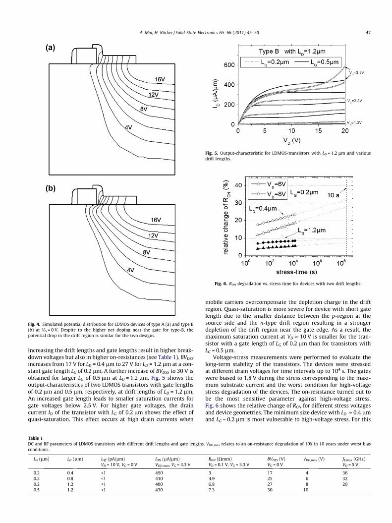
Fig. 4. Simulated potential distribution for LDMOS devices of type A (a) and type B(b) at VG = 0 V. Despite to the higher net doping near the gate for type-B, thepotential drop in the drift region is similar for the two designs.
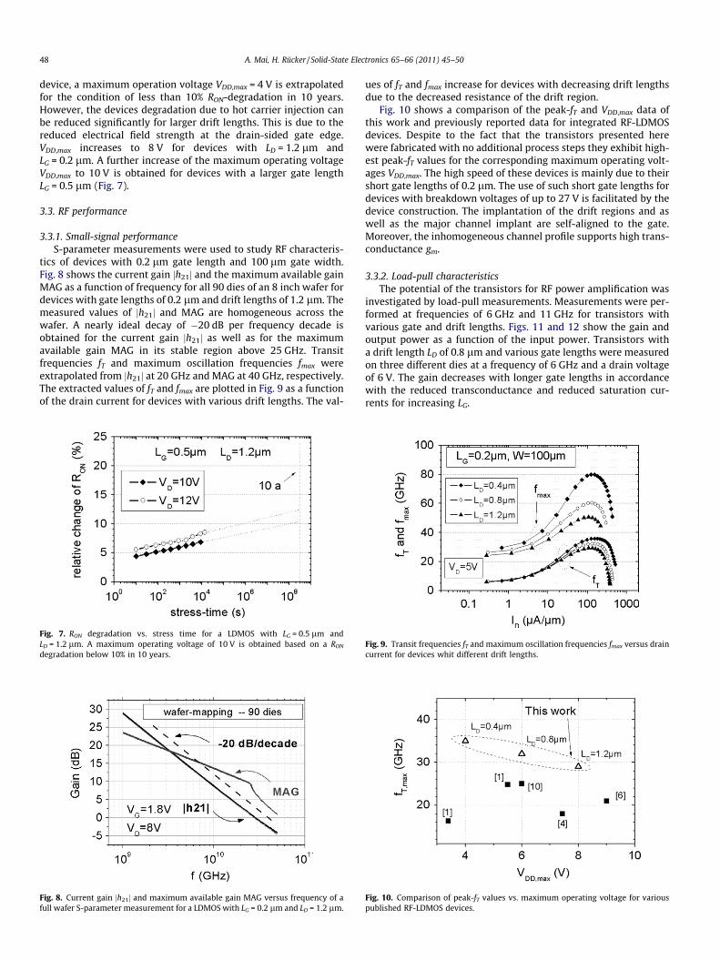
Fig. 5. Output-characteristic for LDMOS-transistors with LD = 1.2 lm and variousdrift lengths.
Fig. 6. RON degradation vs. stress time for devices with two drift lengths.
A. Mai, H. Rücker / Solid-State Electronics 65–66 (2011) 45–50 47
Increasing the drift lengths and gate lengths result in higher break-down voltages but also in higher on-resistances (see Table 1). BVDSS
increases from 17 V for LD = 0.4 lm to 27 V for LD = 1.2 lm at a con-stant gate length LG of 0.2 lm. A further increase of BVDSS to 30 V isobtained for larger LG of 0.5 lm at LD = 1.2 lm. Fig. 5 shows theoutput-characteristics of two LDMOS transistors with gate lengthsof 0.2 lm and 0.5 lm, respectively, at drift lengths of LD = 1.2 lm.An increased gate length leads to smaller saturation currents forgate voltages below 2.5 V. For higher gate voltages, the draincurrent ID of the transistor with LG of 0.2 lm shows the effect ofquasi-saturation. This effect occurs at high drain currents when
Table 1DC and RF parameters of LDMOS transistors with different drift lengths and gate lengthsconditions.
LG (lm) LD (lm) IOff (pA/lm) ION (lA/lm)VD = 10 V, VG = 0 V VDD,max, VG = 3.3 V
0.2 0.4 <1 4500.2 0.8 <1 4300.2 1.2 <1 4000.5 1.2 <1 430
mobile carriers overcompensate the depletion charge in the driftregion. Quasi-saturation is more severe for device with short gatelength due to the smaller distance between the p-region at thesource side and the n-type drift region resulting in a strongerdepletion of the drift region near the gate edge. As a result, themaximum saturation current at VD � 10 V is smaller for the tran-sistor with a gate length of LG of 0.2 lm than for transistors withLG = 0.5 lm.
Voltage-stress measurements were performed to evaluate thelong-term stability of the transistors. The devices were stressedat different drain voltages for time intervals up to 104 s. The gateswere biased to 1.8 V during the stress corresponding to the maxi-mum substrate current and the worst condition for high-voltagestress degradation of the devices. The on-resistance turned out tobe the most sensitive parameter against high-voltage stress.Fig. 6 shows the relative change of RON for different stress voltagesand device geometries. The minimum size device with LD = 0.4 lmand LG = 0.2 lm is most vulnerable to high-voltage stress. For this
. VDD,max relates to an on-resistance degradation of 10% in 10 years under worst bias
RON (Xmm) BVDSS (V) VDD,max (V) fT,max (GHz)VD = 0.1 V, VG = 3.3 V VG = 0 V VD = 5 V
3 17 4 364.9 25 6 326.8 27 8 297.3 30 10
48 A. Mai, H. Rücker / Solid-State Electronics 65–66 (2011) 45–50
device, a maximum operation voltage VDD,max = 4 V is extrapolatedfor the condition of less than 10% RON-degradation in 10 years.However, the devices degradation due to hot carrier injection canbe reduced significantly for larger drift lengths. This is due to thereduced electrical field strength at the drain-sided gate edge.VDD,max increases to 8 V for devices with LD = 1.2 lm andLG = 0.2 lm. A further increase of the maximum operating voltageVDD,max to 10 V is obtained for devices with a larger gate lengthLG = 0.5 lm (Fig. 7).
3.3. RF performance
3.3.1. Small-signal performanceS-parameter measurements were used to study RF characteris-
tics of devices with 0.2 lm gate length and 100 lm gate width.Fig. 8 shows the current gain jh21j and the maximum available gainMAG as a function of frequency for all 90 dies of an 8 inch wafer fordevices with gate lengths of 0.2 lm and drift lengths of 1.2 lm. Themeasured values of jh21j and MAG are homogeneous across thewafer. A nearly ideal decay of �20 dB per frequency decade isobtained for the current gain jh21j as well as for the maximumavailable gain MAG in its stable region above 25 GHz. Transitfrequencies fT and maximum oscillation frequencies fmax wereextrapolated from jh21j at 20 GHz and MAG at 40 GHz, respectively.The extracted values of fT and fmax are plotted in Fig. 9 as a functionof the drain current for devices with various drift lengths. The val-
Fig. 7. RON degradation vs. stress time for a LDMOS with LG = 0.5 lm andLD = 1.2 lm. A maximum operating voltage of 10 V is obtained based on a RON
degradation below 10% in 10 years.
Fig. 8. Current gain jh21j and maximum available gain MAG versus frequency of afull wafer S-parameter measurement for a LDMOS with LG = 0.2 lm and LD = 1.2 lm.
ues of fT and fmax increase for devices with decreasing drift lengthsdue to the decreased resistance of the drift region.
Fig. 10 shows a comparison of the peak-fT and VDD,max data ofthis work and previously reported data for integrated RF-LDMOSdevices. Despite to the fact that the transistors presented herewere fabricated with no additional process steps they exhibit high-est peak-fT values for the corresponding maximum operating volt-ages VDD,max. The high speed of these devices is mainly due to theirshort gate lengths of 0.2 lm. The use of such short gate lengths fordevices with breakdown voltages of up to 27 V is facilitated by thedevice construction. The implantation of the drift regions and aswell as the major channel implant are self-aligned to the gate.Moreover, the inhomogeneous channel profile supports high trans-conductance gm.
3.3.2. Load-pull characteristicsThe potential of the transistors for RF power amplification was
investigated by load-pull measurements. Measurements were per-formed at frequencies of 6 GHz and 11 GHz for transistors withvarious gate and drift lengths. Figs. 11 and 12 show the gain andoutput power as a function of the input power. Transistors witha drift length LD of 0.8 lm and various gate lengths were measuredon three different dies at a frequency of 6 GHz and a drain voltageof 6 V. The gain decreases with longer gate lengths in accordancewith the reduced transconductance and reduced saturation cur-rents for increasing LG.
Fig. 9. Transit frequencies fT and maximum oscillation frequencies fmax versus draincurrent for devices whit different drift lengths.
Fig. 10. Comparison of peak-fT values vs. maximum operating voltage for variouspublished RF-LDMOS devices.
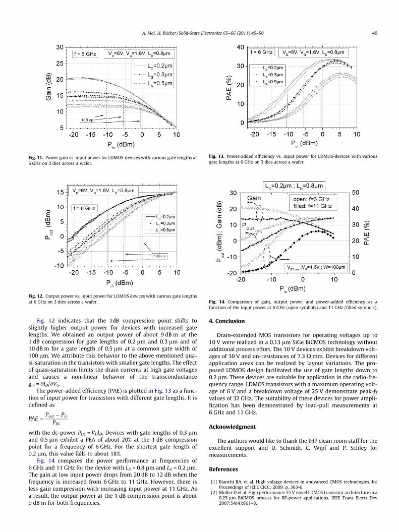
Fig. 11. Power gain vs. input power for LDMOS-devices with various gate lengths at6 GHz on 3 dies across a wafer.
Fig. 12. Output power vs. input power for LDMOS devices with various gate lengthsat 6 GHz on 3 dies across a wafer.
Fig. 13. Power-added efficiency vs. input power for LDMOS-devices with variousgate lengths at 6 GHz on 3 dies across a wafer.
Fig. 14. Comparison of gain, output power and power-added efficiency as afunction of the input power at 6 GHz (open symbols) and 11 GHz (filled symbols).
A. Mai, H. Rücker / Solid-State Electronics 65–66 (2011) 45–50 49
Fig. 12 indicates that the 1dB compression point shifts toslightly higher output power for devices with increased gatelengths. We obtained an output power of about 9 dB m at the1 dB compression for gate lengths of 0.2 lm and 0.3 lm and of10 dB m for a gate length of 0.5 lm at a common gate width of100 lm. We attribute this behavior to the above mentioned qua-si-saturation in the transistors with smaller gate lengths. The effectof quasi-saturation limits the drain currents at high gate voltagesand causes a non-linear behavior of the transconductancegm = @ID/@VG.
The power-added efficiency (PAE) is plotted in Fig. 13 as a func-tion of input power for transistors with different gate lengths. It isdefined as
PAE ¼ Pout � Pin
PDC
with the dc-power PDC = VDID. Devices with gate lengths of 0.3 lmand 0.5 lm exhibit a PEA of about 20% at the 1 dB compressionpoint for a frequency of 6 GHz. For the shortest gate length of0.2 lm, this value falls to about 18%.
Fig. 14 compares the power performance at frequencies of6 GHz and 11 GHz for the device with LD = 0.8 lm and LG = 0.2 lm.The gain at low input power drops from 20 dB to 12 dB when thefrequency is increased from 6 GHz to 11 GHz. However, there isless gain compression with increasing input power at 11 GHz. Asa result, the output power at the 1 dB compression point is about9 dB m for both frequencies.
4. Conclusion
Drain-extended MOS transistors for operating voltages up to10 V were realized in a 0.13 lm SiGe BiCMOS technology withoutadditional process effort. The 10 V devices exhibit breakdown volt-ages of 30 V and on-resistances of 7.3 X mm. Devices for differentapplication areas can be realized by layout variations. The pro-posed LDMOS design facilitated the use of gate lengths down to0.2 lm. These devices are suitable for application in the radio-fre-quency range. LDMOS transistors with a maximum operating volt-age of 6 V and a breakdown voltage of 25 V demonstrate peak-fT
values of 32 GHz. The suitability of these devices for power ampli-fication has been demonstrated by load-pull measurements at6 GHz and 11 GHz.
Acknowledgment
The authors would like to thank the IHP clean room staff for theexcellent support and D. Schmidt, C. Wipf and P. Schley formeasurements.
References
[1] Bianchi RA, et al. High voltage devices in andvanced CMOS technologies. In:Proceedings of IEEE CICC; 2009. p. 363-6.
[2] Muller D et al. High performance 15 V novel LDMOS transistor architecture in a0.25 lm BiCMOS process for RF-power applications. IEEE Trans Electr Dev2007;54(4):861–8.

50 A. Mai, H. Rücker / Solid-State Electronics 65–66 (2011) 45–50
[3] Szelag B, et al. Integration and optimization of a high performance RF lateralDMOS in an advanced BICMOS technology. In: Proceedings of IEEE ESSDERC;2003. p. 39–42.
[4] Lee Z, et al. A modular 0.18 lm Analog RFCMOS technology comprising 32 GHzFT RF-LDMOS and 40 V complementary MOSFET devices. In: Proceedings ofIEEE BCTM; 2006. p. 126–9.
[5] Ehwald KE, et al. A two mask complementary LDMOS module integrated in a0.25 lm SiGe:C-BiCMOS platform. In: Proceedings of IEEE ESSDERC; 2004. p.121–4.
[6] Mohapatra NR, et al. A complementary RF-LDMOS architecture compatiblewith a 0.13 lm CMOS technology. In: Proceedings of IEEE ISPSD; 2006. p. 37–40.
[7] Baldwin G, et al. 90 nm CMOS RF technology with 9.0 V I/O capability forsingle-chip radio. Digest of symposium VLSI technology; 2003. p. 62–3.
[8] Mitros JC et al. High-voltage drain extended MOS transistor for 0.18-lm logicCMOS process. IEEE Trans Electr Dev 2001;48(8):1751–5.
[9] Yan T et al. Cost effective integrated RF power transistor in 0.18-lm CMOStechnology. IEEE Electr Dev Lett 2004;27(10):856–8.
[10] Mai A, et al. Cost-effective integration of RF-LDMOS transistors in 0.13 lmCMOS technology. In: Proceedings of IEEE SiRF; 2009. p. 124–8.
[11] Rücker H et al. A 0.13 lm SiGe BiCMOS technology featuring fT/fMAX of 240/330 GHz and gate delays below 3 ps. IEEE J Solid-State Circ2010;45(9):1678–86.
[12] Mohapatra NR, et al. The impact of Channel engineering on the performanceand reliability of LDMOS transistors. In: Proceedings of IEEE ESSDERC; 2005. p.481–4.