Embed Size (px)
Citation preview
DRAFT
DR
T DR
DR
RAF
DR
FTD
DR
DRA
UNCLASSIF
IED
AFT DRAF
AFT DRAFT DRAFT D
AFTDRAFT
DRAFTDRAFT
DRA
AFT DRAFT DRAFT DRAFT DRAFT DRAFT1. General description
The TEF6621 is an AM/FM radio including Phase-Locked Loop (PLL) tuning system. Thesystem is designed in such a way, that it can be used as a world-wide tuner coveringcommon FM and AM bands for radio reception. All functions are controlled by the I2C-bus.Besides the basic feature set it provides a good weak signal processing function.
2. Features
n FM tuner for Japan, Europe and US reception
n AM tuner for Long Wave (LW) and Medium Wave (MW) reception
n Integrated AM Radio Frequency (RF) selectivity
n Integrated PLL tuning system; controlled via I2C-bus
n Fully integrated Local Oscillator (LO)
n No alignment needed
n Very easy application on the main board
n No critical RF components
n Fully integrated Intermediate Frequency (IF) filters and FM stereo decoder
n Fully integrated FM noise blanker
n Field strength (LEVEL), multipath [Wideband AM (WAM)] and noise [UltraSonic Noise(USN)] dependent stereo blend
n Field strength (LEVEL), multipath (WAM) and noise (USN) dependent High-CutControl (HCC)
n Field strength (LEVEL), multipath (WAM) and noise (USN) dependent soft mute
n Single power supply
TEF6621Tuner on main-board ICRev. 01.04 — 7 August 2008 Objective data sheet
DRAFT
DRAFT DRAFT DR
DRAFT DRAFT DRAF
RAF
DRAFTDRAFT
DRAF
FTD
DRAFT DRAFT DRAF
DRA
NXP Semiconductors TEF6621Tuner on main-board IC
T DT
DRAFTDRA
T DRAFT DRAFT DRAFT
UNCLASSIF
IED
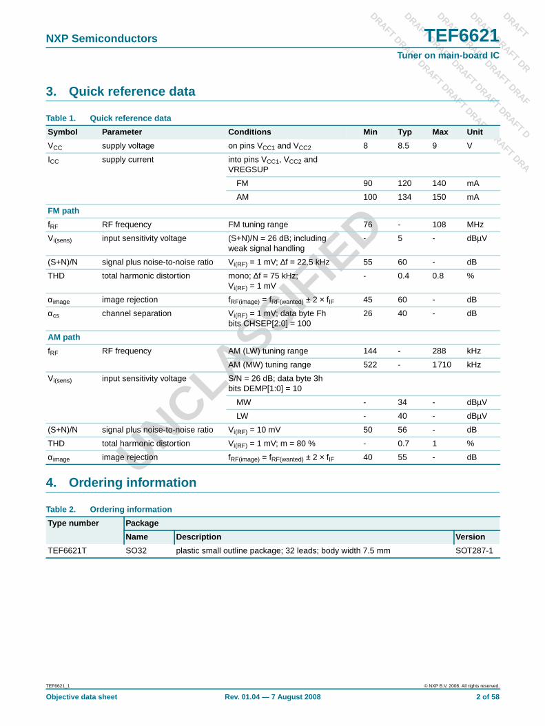
3. Quick reference data
4. Ordering information
Table 1. Quick reference data
Symbol Parameter Conditions Min Typ Max Unit
VCC supply voltage on pins VCC1 and VCC2 8 8.5 9 V
ICC supply current into pins VCC1, VCC2 andVREGSUP
FM 90 120 140 mA
AM 100 134 150 mA
FM path
fRF RF frequency FM tuning range 76 - 108 MHz
Vi(sens) input sensitivity voltage (S+N)/N = 26 dB; includingweak signal handling
- 5 - dBµV
(S+N)/N signal plus noise-to-noise ratio Vi(RF) = 1 mV; ∆f = 22.5 kHz 55 60 - dB
THD total harmonic distortion mono; ∆f = 75 kHz;Vi(RF) = 1 mV
- 0.4 0.8 %
αimage image rejection fRF(image) = fRF(wanted) ± 2 × fIF 45 60 - dB
αcs channel separation Vi(RF) = 1 mV; data byte Fhbits CHSEP[2:0] = 100
26 40 - dB
AM path
fRF RF frequency AM (LW) tuning range 144 - 288 kHz
AM (MW) tuning range 522 - 1710 kHz
Vi(sens) input sensitivity voltage S/N = 26 dB; data byte 3hbits DEMP[1:0] = 10
MW - 34 - dBµV
LW - 40 - dBµV
(S+N)/N signal plus noise-to-noise ratio Vi(RF) = 10 mV 50 56 - dB
THD total harmonic distortion Vi(RF) = 1 mV; m = 80 % - 0.7 1 %
αimage image rejection fRF(image) = fRF(wanted) ± 2 × fIF 40 55 - dB
Table 2. Ordering information
Type number Package
Name Description Version
TEF6621T SO32 plastic small outline package; 32 leads; body width 7.5 mm SOT287-1
TEF6621_1 © NXP B.V. 2008. All rights reserved.
Objective data sheet Rev. 01.04 — 7 August 2008 2 of 58
DRAFT
DRAFT DRAFT DR
DRAFT DRAFT DRAF
RAF
DRAFTDRAFT
DRAF
FTD
DRAFT DRAFT DRAF
DRA
NXP Semiconductors TEF6621Tuner on main-board IC
T DT
DRAFTDRA
T DRAFT DRAFT DRAFT
UNCLASSIF
IED
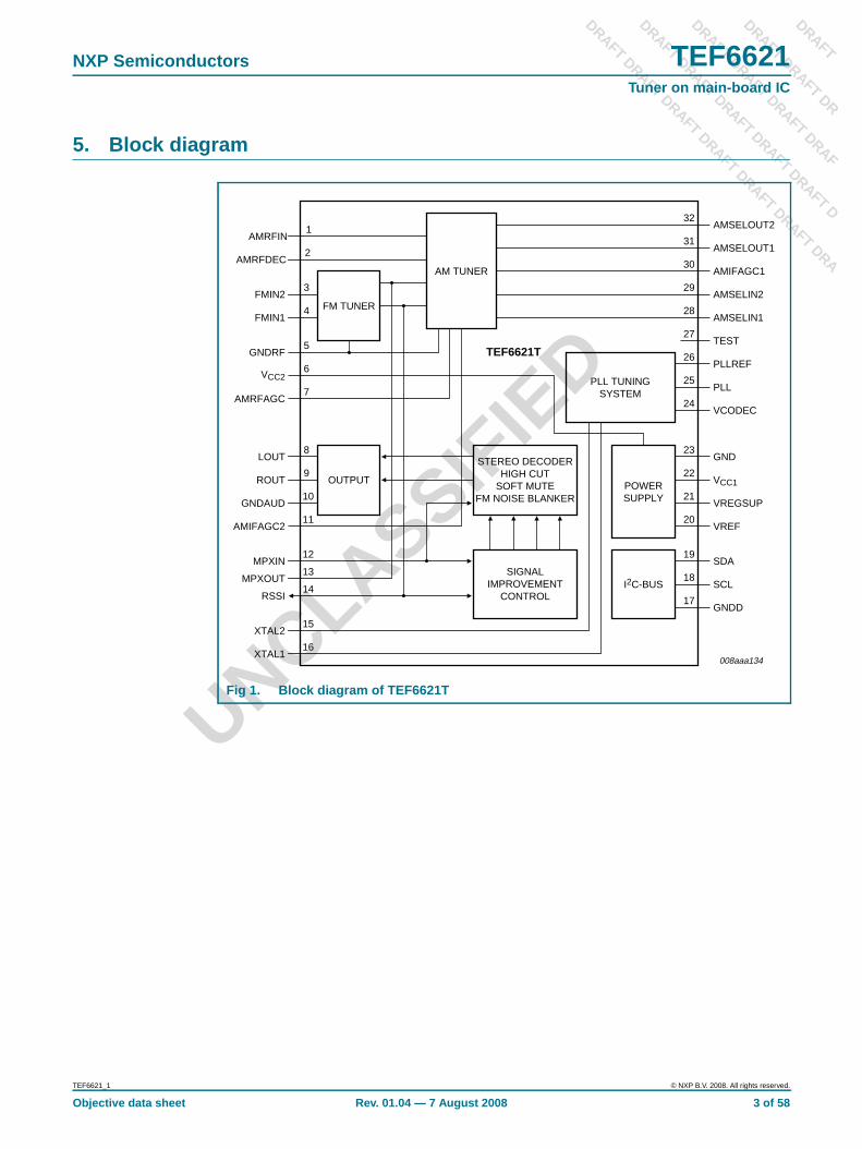
5. Block diagram
Fig 1. Block diagram of TEF6621T
008aaa134
17GNDD
AM TUNER
FM TUNER
OUTPUT
TEF6621T
PLL TUNINGSYSTEM
POWERSUPPLY
I2C-BUS
STEREO DECODERHIGH CUT
SOFT MUTEFM NOISE BLANKER
SIGNALIMPROVEMENT
CONTROL
18SCL
19SDA
20VREF
21VREGSUP
22VCC1
23GND
29AMSELIN2
28AMSELIN1
27TEST
30AMIFAGC1
31AMSELOUT1
32
AMRFIN1
AMRFDEC2
GNDRF5
VCC26
AMRFAGC7
AMIFAGC211
MPXIN12
MPXOUT13
RSSI14
XTAL215
XTAL116
AMSELOUT2
24VCODEC
25PLL
26PLLREF
GNDAUD10
ROUT9
LOUT8
FMIN14
FMIN23
TEF6621_1 © NXP B.V. 2008. All rights reserved.
Objective data sheet Rev. 01.04 — 7 August 2008 3 of 58
DRAFT
DRAFT DRAFT DR
DRAFT DRAFT DRAF
RAF
DRAFTDRAFT
DRAF
FTD
DRAFT DRAFT DRAF
DRA
NXP Semiconductors TEF6621Tuner on main-board IC
T DT
DRAFTDRA
T DRAFT DRAFT DRAFT
UNCLASSIF
IED
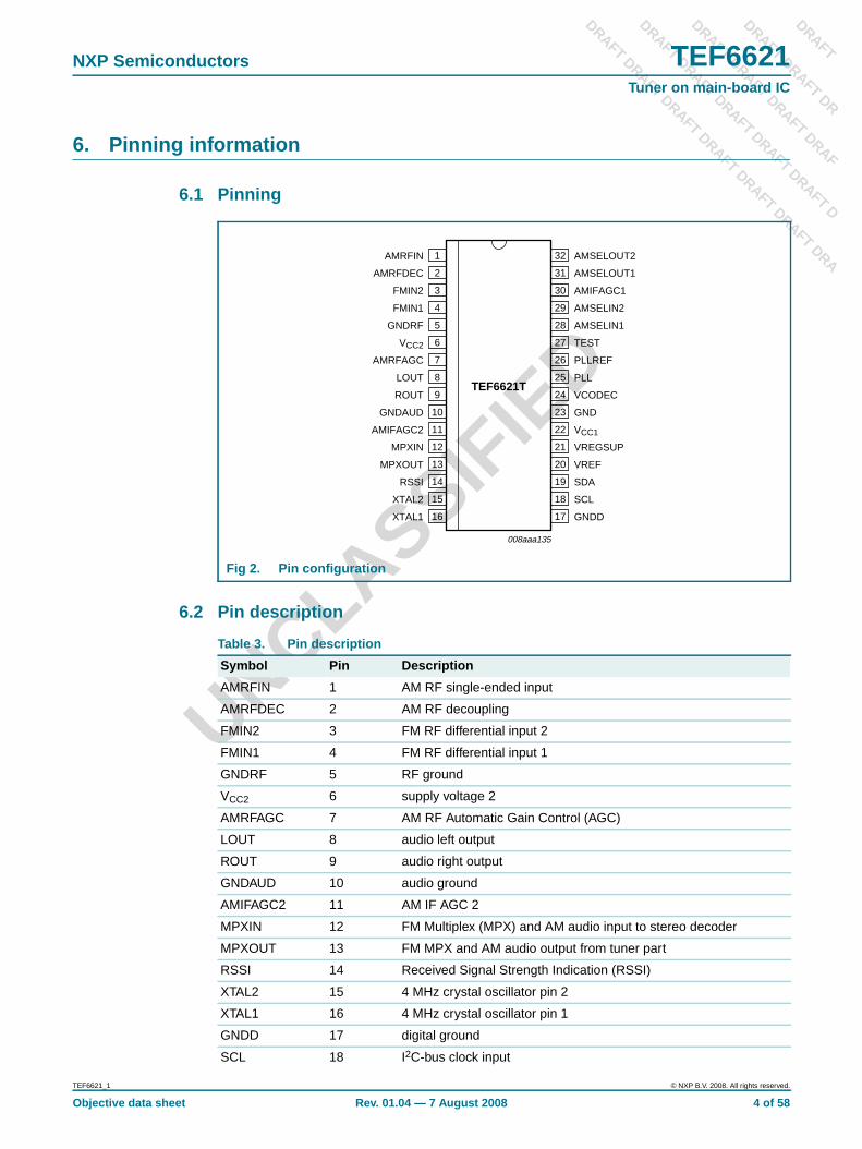
6. Pinning information
6.1 Pinning
6.2 Pin description
Fig 2. Pin configuration
TEF6621T
AMRFIN AMSELOUT2
AMRFDEC AMSELOUT1
FMIN2 AMIFAGC1
FMIN1 AMSELIN2
GNDRF AMSELIN1
VCC2 TEST
AMRFAGC PLLREF
LOUT PLL
ROUT VCODEC
GNDAUD GND
AMIFAGC2 VCC1
MPXIN VREGSUP
MPXOUT VREF
RSSI SDA
XTAL2 SCL
XTAL1 GNDD
008aaa135
1
2
3
4
5
6
7
8
9
10
11
12
13
14
15
16
18
17
20
19
22
21
24
23
26
25
32
31
30
29
28
27
Table 3. Pin description
Symbol Pin Description
AMRFIN 1 AM RF single-ended input
AMRFDEC 2 AM RF decoupling
FMIN2 3 FM RF differential input 2
FMIN1 4 FM RF differential input 1
GNDRF 5 RF ground
VCC2 6 supply voltage 2
AMRFAGC 7 AM RF Automatic Gain Control (AGC)
LOUT 8 audio left output
ROUT 9 audio right output
GNDAUD 10 audio ground
AMIFAGC2 11 AM IF AGC 2
MPXIN 12 FM Multiplex (MPX) and AM audio input to stereo decoder
MPXOUT 13 FM MPX and AM audio output from tuner part
RSSI 14 Received Signal Strength Indication (RSSI)
XTAL2 15 4 MHz crystal oscillator pin 2
XTAL1 16 4 MHz crystal oscillator pin 1
GNDD 17 digital ground
SCL 18 I2C-bus clock input
TEF6621_1 © NXP B.V. 2008. All rights reserved.
Objective data sheet Rev. 01.04 — 7 August 2008 4 of 58
DRAFT
DRAFT DRAFT DR
DRAFT DRAFT DRAF
RAF
DRAFTDRAFT
DRAF
FTD
DRAFT DRAFT DRAF
DRA
NXP Semiconductors TEF6621Tuner on main-board IC
T DT
DRAFTDRA
T DRAFT DRAFT DRAFT
UNCLASSIF
IED
7. Functional description
7.1 FM tunerThe RF input signal is mixed to a low IF with inherent image suppression. The IF signal isfiltered and demodulated. The complete signal path is fully integrated.
7.2 AM tunerThe RF signal is filtered and mixed to a low IF with inherent image suppression. The IFsignals are filtered and demodulated. The signal path is highly integrated.
7.3 PLL tuning systemThe PLL tuning system includes a fully integrated VCO. To avoid problems with unwantedsignals on image side, the receiver controls automatically high-side or low-side injection.
7.4 FM stereo decoderThe MPX signal from the FM tuner is translated by the stereo decoder into a left and rightaudio channel. Good channel separation is achieved without alignment.
7.5 Weak signal processing and noise blankerThe reception quality of the station received is measured by a combination of detectors:field strength (LEVEL), multipath (WAM) and noise (USN). The audio processing functionssoft mute, HCC and stereo blend are controlled accordingly to maintain the best possibleaudio quality in case of poor signal conditions. Audio disturbances like e.g. ignition noiseare suppressed by the noise blanker circuit, using USN detection on MPX and spikedetection on the level signal.
SDA 19 I2C-bus data input and output
VREF 20 reference voltage decoupling
VREGSUP 21 supply voltage internal voltage regulators
VCC1 22 supply voltage 1
GND 23 ground
VCODEC 24 decoupling for Voltage-Controlled Oscillator (VCO) supply voltage
PLL 25 PLL tuning voltage
PLLREF 26 PLL reference voltage
TEST 27 test pin; leave open in normal operation
AMSELIN1 28 AM selectivity input 1
AMSELIN2 29 AM selectivity input 2
AMIFAGC1 30 AM IF AGC 1
AMSELOUT1 31 AM selectivity output 1
AMSELOUT2 32 AM selectivity output 2
Table 3. Pin description …continued
Symbol Pin Description
TEF6621_1 © NXP B.V. 2008. All rights reserved.
Objective data sheet Rev. 01.04 — 7 August 2008 5 of 58
DRAFT
DRAFT DRAFT DR
DRAFT DRAFT DRAF
RAF
DRAFTDRAFT
DRAF
FTD
DRAFT DRAFT DRAF
DRA
NXP Semiconductors TEF6621Tuner on main-board IC
T DT
DRAFTDRA
T DRAFT DRAFT DRAFT
UNCLASSIF
IED
9. Limiting values
[1] Class 2 according to JESD22-A114.
[2] Class B according to EIA/JESD22-A115.
10. Thermal characteristics
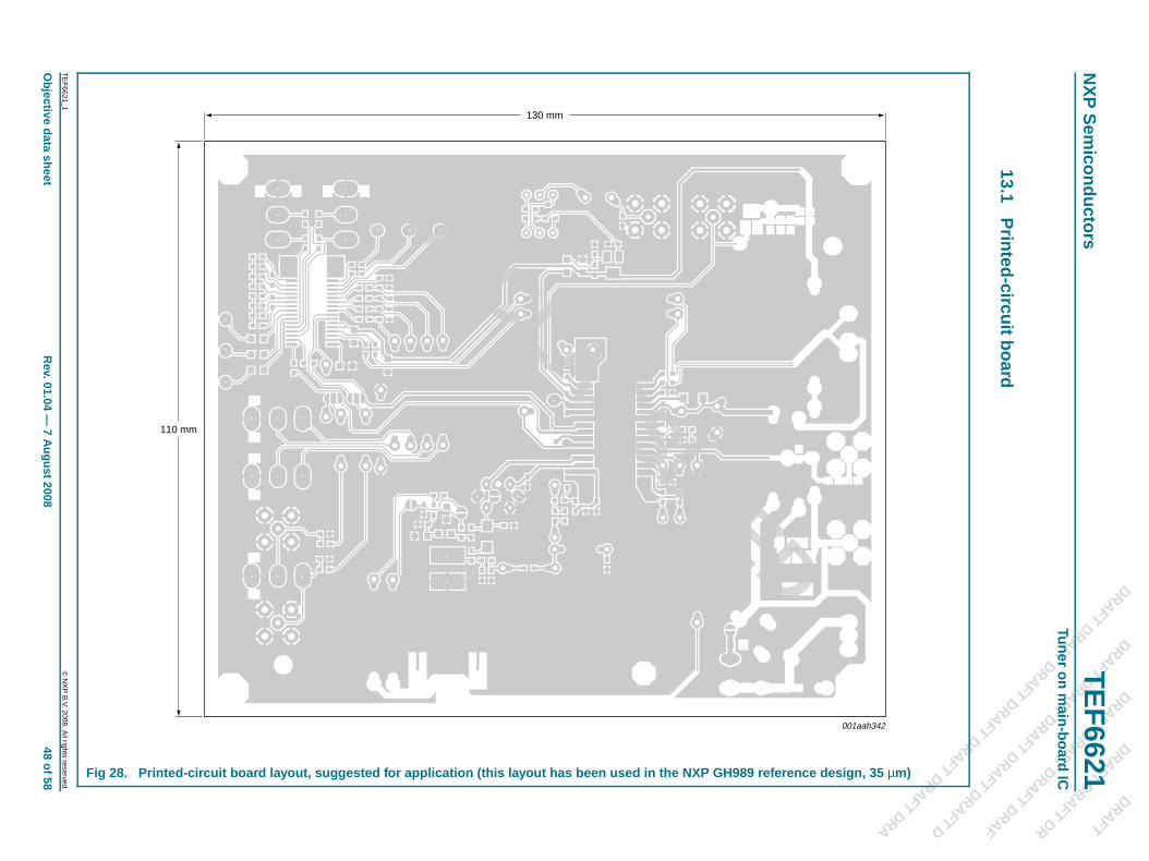
[1] The thermal resistance depends strongly on the PCB design. An application different to Figure 28 must ensure that the thermalresistance is below 54 K/W to avoid violation of the maximum junction temperature; see Table 57.
Table 57. Limiting valuesIn accordance with the Absolute Maximum Rating System (IEC 60134).
Symbol Parameter Conditions Min Max Unit
VCC supply voltage on pins VCC1 and VCC2 −0.3 +10 V
∆VCCn voltage difference between anysupply pins
between pins VCC1 and VCC2 −0.3 +0.3 V
VSCL voltage on pin SCL −0.3 +6 V
VSDA voltage on pin SDA −0.3 +6 V
VAMRFDEC voltage on pin AMRFDEC −0.3 +6 V
VAMRFIN voltage on pin AMRFIN −0.3 +6 V
VAMRFAGC voltage on pin AMRFAGC −0.3 +6 V
VAMIFAGC2 voltage on pin AMIFAGC2 −0.3 +6 V
VRSSI RSSI voltage −0.3 +6 V
VVCODEC voltage on pin VCODEC −0.3 +6 V
VPLL voltage on pin PLL −0.3 +6 V
VPLLREF voltage on pin PLLREF −0.3 +6 V
VTEST voltage on pin TEST −0.3 +6 V
VAMIFAGC1 voltage on pin AMIFAGC1 −0.3 +6 V
VVREF voltage on pin VREF −0.3 +6 V
Vn voltage on any other pin −0.3 +VCC V
Tstg storage temperature −40 +150 °C
Tamb ambient temperature −20 +85 °C
Tj junction temperature - 150 °C
Vesd electrostatic discharge voltage human body model [1] −2000 +2000 V
machine model [2] −200 +200 V
Table 58. Thermal characteristics
Symbol Parameter Conditions Typ Unit
Rth(j-a) thermal resistance fromjunction to ambient
in free air; single layer board with acopper thickness of 35 µm;see Figure 28
[1] 48 K/W
Ψj-top thermal characterizationparameter from junction to topof package
4.5 K/W
TEF6621_1 © NXP B.V. 2008. All rights reserved.
Objective data sheet Rev. 01.04 — 7 August 2008 39 of 58
DRAFT
DRAFT DRAFT DR
DRAFT DRAFT DRAF
RAF
DRAFTDRAFT
DRAF
FTD
DRAFT DRAFT DRAF
DRA
NXP Semiconductors TEF6621Tuner on main-board IC
T DT
DRAFTDRA
T DRAFT DRAFT DRAFT
UNCLASSIF
IED
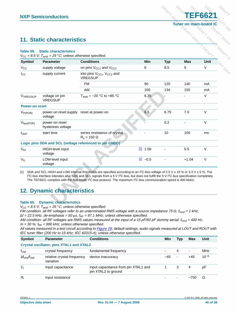
11. Static characteristics
[1] SDA and SCL HIGH and LOW internal thresholds are specified according to an I2C-bus voltage of 2.5 V ± 10 % or 3.3 V ± 5 %. TheI2C-bus interface tolerates also SDA and SCL signals from a 5 V I2C-bus, but does not fulfill the 5 V I2C-bus specification completely.The TEF6621 complies with the fast-mode I2C-bus protocol. The maximum I2C-bus communication speed is 400 kbit/s.
12. Dynamic characteristics
Table 59. Static characteristicsVCC = 8.5 V; Tamb = 25 °C; unless otherwise specified.
Symbol Parameter Conditions Min Typ Max Unit
VCC supply voltage on pins VCC1 and VCC2 8 8.5 9 V
ICC supply current into pins VCC1, VCC2 andVREGSUP
FM 90 120 140 mA
AM 100 134 150 mA
VVREGSUP voltage on pinVREGSUP
Tamb = −20 °C to +85 °C 6.35 - - V
Power-on reset
VP(POR) power-on reset supplyvoltage
reset at power-on 6.5 6.75 7.0 V
Vhys(POR) power-on resethysteresis voltage
- 0.2 - V
tstart start time series resistance of crystalRs = 150 Ω
- 10 100 ms
Logic pins SDA and SCL (voltage referenced to pin GNDD)
VIH HIGH-level inputvoltage
[1] 1.58 - 5.5 V
VIL LOW-level inputvoltage
[1] −0.5 - +1.04 V
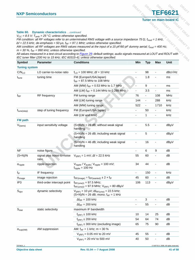
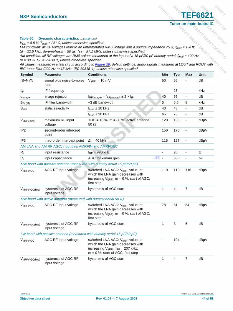
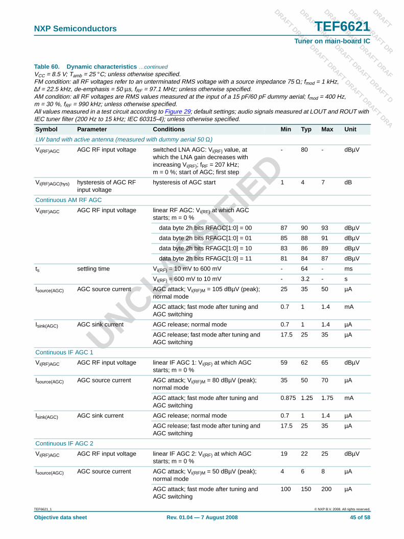
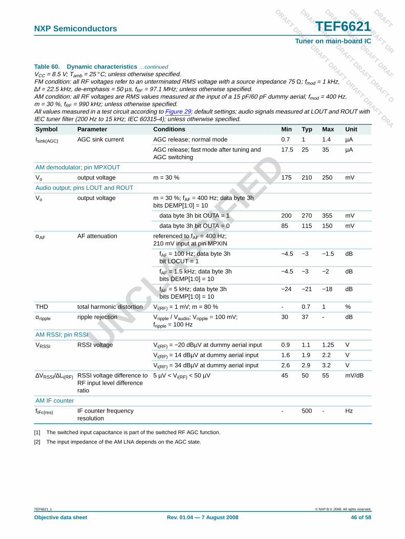
Table 60. Dynamic characteristicsVCC = 8.5 V; Tamb = 25 °C; unless otherwise specified.FM condition: all RF voltages refer to an unterminated RMS voltage with a source impedance 75 Ω; fmod = 1 kHz,∆f = 22.5 kHz, de-emphasis = 50 µs, fRF = 97.1 MHz; unless otherwise specified.AM condition: all RF voltages are RMS values measured at the input of a 15 pF/60 pF dummy aerial; fmod = 400 Hz,m = 30 %, fRF = 990 kHz; unless otherwise specified.All values measured in a test circuit according to Figure 29; default settings; audio signals measured at LOUT and ROUT withIEC tuner filter (200 Hz to 15 kHz; IEC 60315-4); unless otherwise specified.
Symbol Parameter Conditions Min Typ Max Unit
Crystal oscillator; pins XTAL1 and XTAL2
fxtal crystal frequency fundamental frequency - 4 - MHz
∆fxtal/fxtal relative crystal frequencyvariation
device inaccuracy −45 - +45 10−6
Ci input capacitance input capacitance from pin XTAL1 andpin XTAL2 to ground
1 3 4 pF
Ri input resistance - - −750 Ω
TEF6621_1 © NXP B.V. 2008. All rights reserved.
Objective data sheet Rev. 01.04 — 7 August 2008 40 of 58
DRAFT
DRAFT DRAFT DR
DRAFT DRAFT DRAF
RAF
DRAFTDRAFT
DRAF
FTD
DRAFT DRAFT DRAF
DRA
NXP Semiconductors TEF6621Tuner on main-board IC
T DT
DRAFTDRA
T DRAFT DRAFT DRAFT
UNCLASSIF
IED
Tuning system
C/NLO LO carrier-to-noise ratio fLO = 100 MHz; ∆f = 10 kHz - 98 - dBc/√Hz
ttune tuning time FM (Europe/USA/Japan)fRF = 87.5 MHz to 108 MHz
- 1.8 - ms
AM (MW) fRF = 0.53 MHz to 1.7 MHz - 9 - ms
AM (LW) fRF = 0.144 MHz to 0.288 MHz - 3.5 - ms
fRF RF frequency FM tuning range 76 - 108 MHz
AM (LW) tuning range 144 - 288 kHz
AM (MW) tuning range 522 - 1710 kHz
ftune(step) step of tuning frequency FM (Europe/USA/Japan) - 50 - kHz
AM (LW and MW) - 1 - kHz
FM path
Vi(sens) input sensitivity voltage (S+N)/N = 26 dB; without weak signalhandling
- 5.5 - dBµV
(S+N)/N = 26 dB; including weak signalhandling
- 5 - dBµV
(S+N)/N = 46 dB; including weak signalhandling
- 16 - dBµV
NF noise figure - 6 9 dB
(S+N)/N signal plus noise-to-noiseratio
Vi(RF) = 1 mV; ∆f = 22.5 kHz 55 60 - dB
αripple ripple rejection Vripple / Vaudio; Vripple = 100 mV;fripple = 100 Hz
34 44 - dB
fIF IF frequency - 150 - kHz
αimage image rejection fRF(image) = fRF(wanted) ± 2 × fIF 45 60 - dB
IP3 third-order intercept point fRF(unw)1 = 97.5 MHz;fRF(unw)2 = 97.9 MHz; Vi(RF) = 80 dBµV
106 113 - dBµV
Sdyn dynamic selectivity Vi(RF) = 10 µV; ∆fRF(unw) = 22.5 kHz;(S+N)/N = 26 dB; mono; fAF = 1 kHz
∆fRF = 100 kHz - 3 - dB
∆fRF = 200 kHz - 55 - dB
Sstat static selectivity maximum IF bandwidth
fi(RF) ± 100 kHz 10 14 25 dB
fi(RF) ± 200 kHz 54 64 74 dB
fi(RF) ± 300 kHz (excluding image) 65 75 90 dB
αsup(AM) AM suppression AM: fAF = 1 kHz; m = 30 %
Vi(RF) = 0.05 mV to 20 mV 45 55 - dB
Vi(RF) = 20 mV to 500 mV 40 50 - dB
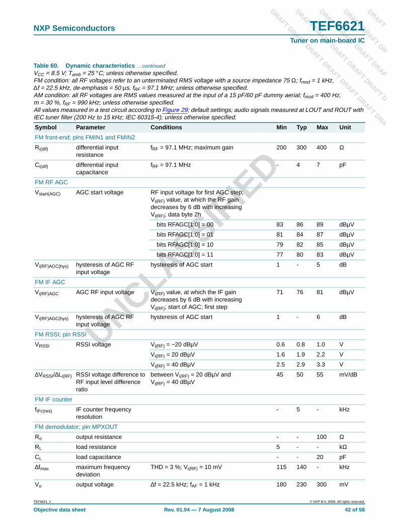
Table 60. Dynamic characteristics …continuedVCC = 8.5 V; Tamb = 25 °C; unless otherwise specified.FM condition: all RF voltages refer to an unterminated RMS voltage with a source impedance 75 Ω; fmod = 1 kHz,∆f = 22.5 kHz, de-emphasis = 50 µs, fRF = 97.1 MHz; unless otherwise specified.AM condition: all RF voltages are RMS values measured at the input of a 15 pF/60 pF dummy aerial; fmod = 400 Hz,m = 30 %, fRF = 990 kHz; unless otherwise specified.All values measured in a test circuit according to Figure 29; default settings; audio signals measured at LOUT and ROUT withIEC tuner filter (200 Hz to 15 kHz; IEC 60315-4); unless otherwise specified.
Symbol Parameter Conditions Min Typ Max Unit
TEF6621_1 © NXP B.V. 2008. All rights reserved.
Objective data sheet Rev. 01.04 — 7 August 2008 41 of 58
DRAFT
DRAFT DRAFT DR
DRAFT DRAFT DRAF
RAF
DRAFTDRAFT
DRAF
FTD
DRAFT DRAFT DRAF
DRA
NXP Semiconductors TEF6621Tuner on main-board IC
T DT
DRAFTDRA
T DRAFT DRAFT DRAFT
UNCLASSIF
IED
FM front-end; pins FMIN1 and FMIN2
Ri(dif) differential inputresistance
fRF = 97.1 MHz; maximum gain 200 300 400 Ω
Ci(dif) differential inputcapacitance
fRF = 97.1 MHz - 4 7 pF
FM RF AGC
Vstart(AGC) AGC start voltage RF input voltage for first AGC step;Vi(RF) value, at which the RF gaindecreases by 6 dB with increasingVi(RF); data byte 2h
bits RFAGC[1:0] = 00 83 86 89 dBµV
bits RFAGC[1:0] = 01 81 84 87 dBµV
bits RFAGC[1:0] = 10 79 82 85 dBµV
bits RFAGC[1:0] = 11 77 80 83 dBµV
Vi(RF)AGC(hys) hysteresis of AGC RFinput voltage
hysteresis of AGC start 1 - 5 dB
FM IF AGC
Vi(RF)AGC AGC RF input voltage Vi(RF) value, at which the IF gaindecreases by 6 dB with increasingVi(RF); start of AGC; first step
71 76 81 dBµV
Vi(RF)AGC(hys) hysteresis of AGC RFinput voltage
hysteresis of AGC start 1 - 6 dB
FM RSSI; pin RSSI
VRSSI RSSI voltage Vi(RF) = −20 dBµV 0.6 0.8 1.0 V
Vi(RF) = 20 dBµV 1.6 1.9 2.2 V
Vi(RF) = 40 dBµV 2.5 2.9 3.3 V
∆VRSSI/∆Li(RF) RSSI voltage difference toRF input level differenceratio
between Vi(RF) = 20 dBµV andVi(RF) = 40 dBµV
45 50 55 mV/dB
FM IF counter
fIFc(res) IF counter frequencyresolution
- 5 - kHz
FM demodulator; pin MPXOUT
Ro output resistance - - 100 Ω
RL load resistance 5 - - kΩ
CL load capacitance - - 20 pF
∆fmax maximum frequencydeviation
THD = 3 %; Vi(RF) = 10 mV 115 140 - kHz
Vo output voltage ∆f = 22.5 kHz; fAF = 1 kHz 180 230 300 mV
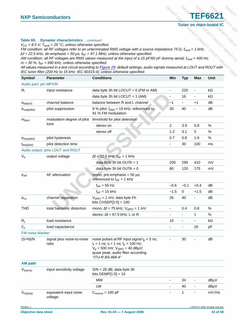
Table 60. Dynamic characteristics …continuedVCC = 8.5 V; Tamb = 25 °C; unless otherwise specified.FM condition: all RF voltages refer to an unterminated RMS voltage with a source impedance 75 Ω; fmod = 1 kHz,∆f = 22.5 kHz, de-emphasis = 50 µs, fRF = 97.1 MHz; unless otherwise specified.AM condition: all RF voltages are RMS values measured at the input of a 15 pF/60 pF dummy aerial; fmod = 400 Hz,m = 30 %, fRF = 990 kHz; unless otherwise specified.All values measured in a test circuit according to Figure 29; default settings; audio signals measured at LOUT and ROUT withIEC tuner filter (200 Hz to 15 kHz; IEC 60315-4); unless otherwise specified.
Symbol Parameter Conditions Min Typ Max Unit
TEF6621_1 © NXP B.V. 2008. All rights reserved.
Objective data sheet Rev. 01.04 — 7 August 2008 42 of 58
DRAFT
DRAFT DRAFT DR
DRAFT DRAFT DRAF
RAF
DRAFTDRAFT
DRAF
FTD
DRAFT DRAFT DRAF
DRA
NXP Semiconductors TEF6621Tuner on main-board IC
T DT
DRAFTDRA
T DRAFT DRAFT DRAFT
UNCLASSIF
IED
Audio part; pin MPXIN
Ri input resistance data byte 3h bit LOCUT = 0 (FM or AM) - 220 - kΩ
data byte 3h bit LOCUT = 1 (AM) - 16 - kΩ
αbal(ch) channel balance balance between R and L channel −1 - +1 dB
αsup(pilot) pilot suppression 9 % pilot; fpilot = 19 kHz; referenced to91 % FM modulation
30 40 - dB
mpilot modulation degree of pilottone
threshold for pilot detection
stereo on 2 3.9 5.8 %
stereo off 1.2 3.1 5 %
αhys(pilot) pilot hysteresis 0.7 0.8 1.6 %
tdet(pilot) pilot detection time - 30 100 ms
Audio output; pins LOUT and ROUT
Vo output voltage ∆f = 22.5 kHz; fAF = 1 kHz
data byte 3h bit OUTA = 1 200 290 410 mV
data byte 3h bit OUTA = 0 80 120 175 mV
αAF AF attenuation mono; pre-emphasis = 50 µs;referenced to fAF = 1 kHz
fAF = 50 Hz −0.6 −0.1 +0.4 dB
fAF = 15 kHz −1.5 0 +1.5 dB
αcs channel separation Vi(RF) = 1 mV; data byte Fhbits CHSEP[2:0] = 100
26 40 - dB
THD total harmonic distortion mono; ∆f = 75 kHz; Vi(RF) = 1 mV - 0.4 0.8 %
stereo; ∆f = 67.5 kHz; L or R - - 1 %
RL load resistance 10 - - kΩ
CL load capacitance - - 20 pF
FM noise blanker
(S+N)/N signal plus noise-to-noiseratio
noise pulses at RF input signal tp = 5 ns;tr < 1 ns; tf < 1 ns; fp = 100 Hz;Vp = 500 mV; Vi(RF) = 40 dBµV;quasi peak; audio filter according“ITU-R BS.468-4”
- 30 - dB
AM path
Vi(sens) input sensitivity voltage S/N = 26 dB; data byte 3hbits DEMP[1:0] = 10
MW - 34 - dBµV
LW - 40 - dBµV
Vn(i)(eq) equivalent input noisevoltage
Csource = 100 pF - 1 - nV/√Hz
Table 60. Dynamic characteristics …continuedVCC = 8.5 V; Tamb = 25 °C; unless otherwise specified.FM condition: all RF voltages refer to an unterminated RMS voltage with a source impedance 75 Ω; fmod = 1 kHz,∆f = 22.5 kHz, de-emphasis = 50 µs, fRF = 97.1 MHz; unless otherwise specified.AM condition: all RF voltages are RMS values measured at the input of a 15 pF/60 pF dummy aerial; fmod = 400 Hz,m = 30 %, fRF = 990 kHz; unless otherwise specified.All values measured in a test circuit according to Figure 29; default settings; audio signals measured at LOUT and ROUT withIEC tuner filter (200 Hz to 15 kHz; IEC 60315-4); unless otherwise specified.
Symbol Parameter Conditions Min Typ Max Unit
TEF6621_1 © NXP B.V. 2008. All rights reserved.
Objective data sheet Rev. 01.04 — 7 August 2008 43 of 58
DRAFT
DRAFT DRAFT DR
DRAFT DRAFT DRAF
RAF
DRAFTDRAFT
DRAF
FTD
DRAFT DRAFT DRAF
DRA
NXP Semiconductors TEF6621Tuner on main-board IC
T DT
DRAFTDRA
T DRAFT DRAFT DRAFT
UNCLASSIF
IED
(S+N)/N signal plus noise-to-noiseratio
Vi(RF) = 10 mV 50 56 - dB
fIF IF frequency - 25 - kHz
αimage image rejection fRF(image) = fRF(wanted) ± 2 × fIF 40 55 - dB
Bfltr(IF) IF filter bandwidth −3 dB bandwidth 5 6.5 8 kHz
Sstat static selectivity ftune ± 10 kHz 40 48 - dB
ftune ± 20 kHz 65 78 - dB
Vi(RF)(max) maximum RF inputvoltage
THD = 10 %; m = 80 %; active antenna50 Ω
120 135 - dBµV
IP2 second-order interceptpoint
150 170 - dBµV
IP3 third-order intercept point ∆f = 40 kHz 116 127 - dBµV
AM LNA and AM RF AGC; input pins AMRFIN and AMRFDEC
Ri input resistance fRF = 990 kHz - 20 - Ω
Ci input capacitance AGC maximum gain [1][2] - 530 - pF
MW band with passive antenna (measured with dummy aerial 15 pF/60 pF)
Vi(RF)AGC AGC RF input voltage switched LNA AGC: Vi(RF) value, atwhich the LNA gain decreases withincreasing Vi(RF); m = 0 %; start of AGC;first step
110 113 116 dBµV
Vi(RF)AGC(hys) hysteresis of AGC RFinput voltage
hysteresis of AGC start 1 4 7 dB
MW band with active antenna (measured with dummy aerial 50 Ω)
Vi(RF)AGC AGC RF input voltage switched LNA AGC: Vi(RF) value, atwhich the LNA gain decreases withincreasing Vi(RF); m = 0 %; start of AGC;first step
78 81 84 dBµV
Vi(RF)AGC(hys) hysteresis of AGC RFinput voltage
hysteresis of AGC start 1 3 6 dB
LW band with passive antenna (measured with dummy aerial 15 pF/60 pF)
Vi(RF)AGC AGC RF input voltage switched LNA AGC: Vi(RF) value, atwhich the LNA gain decreases withincreasing Vi(RF); fRF = 207 kHz;m = 0 %; start of AGC; first step
- 104 - dBµV
Vi(RF)AGC(hys) hysteresis of AGC RFinput voltage
hysteresis of AGC start 1 4 7 dB
Table 60. Dynamic characteristics …continuedVCC = 8.5 V; Tamb = 25 °C; unless otherwise specified.FM condition: all RF voltages refer to an unterminated RMS voltage with a source impedance 75 Ω; fmod = 1 kHz,∆f = 22.5 kHz, de-emphasis = 50 µs, fRF = 97.1 MHz; unless otherwise specified.AM condition: all RF voltages are RMS values measured at the input of a 15 pF/60 pF dummy aerial; fmod = 400 Hz,m = 30 %, fRF = 990 kHz; unless otherwise specified.All values measured in a test circuit according to Figure 29; default settings; audio signals measured at LOUT and ROUT withIEC tuner filter (200 Hz to 15 kHz; IEC 60315-4); unless otherwise specified.
Symbol Parameter Conditions Min Typ Max Unit
TEF6621_1 © NXP B.V. 2008. All rights reserved.
Objective data sheet Rev. 01.04 — 7 August 2008 44 of 58
DRAFT
DRAFT DRAFT DR
DRAFT DRAFT DRAF
RAF
DRAFTDRAFT
DRAF
FTD
DRAFT DRAFT DRAF
DRA
NXP Semiconductors TEF6621Tuner on main-board IC
T DT
DRAFTDRA
T DRAFT DRAFT DRAFT
UNCLASSIF
IED
LW band with active antenna (measured with dummy aerial 50 Ω)
Vi(RF)AGC AGC RF input voltage switched LNA AGC: Vi(RF) value, atwhich the LNA gain decreases withincreasing Vi(RF); fRF = 207 kHz;m = 0 %; start of AGC; first step
- 80 - dBµV
Vi(RF)AGC(hys) hysteresis of AGC RFinput voltage
hysteresis of AGC start 1 4 7 dB
Continuous AM RF AGC
Vi(RF)AGC AGC RF input voltage linear RF AGC: Vi(RF) at which AGCstarts; m = 0 %
data byte 2h bits RFAGC[1:0] = 00 87 90 93 dBµV
data byte 2h bits RFAGC[1:0] = 01 85 88 91 dBµV
data byte 2h bits RFAGC[1:0] = 10 83 86 89 dBµV
data byte 2h bits RFAGC[1:0] = 11 81 84 87 dBµV
ts settling time Vi(RF) = 10 mV to 600 mV - 64 - ms
Vi(RF) = 600 mV to 10 mV - 3.2 - s
Isource(AGC) AGC source current AGC attack; Vi(RF)M = 105 dBµV (peak);normal mode
25 35 50 µA
AGC attack; fast mode after tuning andAGC switching
0.7 1 1.4 mA
Isink(AGC) AGC sink current AGC release; normal mode 0.7 1 1.4 µA
AGC release; fast mode after tuning andAGC switching
17.5 25 35 µA
Continuous IF AGC 1
Vi(RF)AGC AGC RF input voltage linear IF AGC 1: Vi(RF) at which AGCstarts; m = 0 %
59 62 65 dBµV
Isource(AGC) AGC source current AGC attack; Vi(RF)M = 80 dBµV (peak);normal mode
35 50 70 µA
AGC attack; fast mode after tuning andAGC switching
0.875 1.25 1.75 mA
Isink(AGC) AGC sink current AGC release; normal mode 0.7 1 1.4 µA
AGC release; fast mode after tuning andAGC switching
17.5 25 35 µA
Continuous IF AGC 2
Vi(RF)AGC AGC RF input voltage linear IF AGC 2: Vi(RF) at which AGCstarts; m = 0 %
19 22 25 dBµV
Isource(AGC) AGC source current AGC attack; Vi(RF)M = 50 dBµV (peak);normal mode
4 6 8 µA
AGC attack; fast mode after tuning andAGC switching
100 150 200 µA
Table 60. Dynamic characteristics …continuedVCC = 8.5 V; Tamb = 25 °C; unless otherwise specified.FM condition: all RF voltages refer to an unterminated RMS voltage with a source impedance 75 Ω; fmod = 1 kHz,∆f = 22.5 kHz, de-emphasis = 50 µs, fRF = 97.1 MHz; unless otherwise specified.AM condition: all RF voltages are RMS values measured at the input of a 15 pF/60 pF dummy aerial; fmod = 400 Hz,m = 30 %, fRF = 990 kHz; unless otherwise specified.All values measured in a test circuit according to Figure 29; default settings; audio signals measured at LOUT and ROUT withIEC tuner filter (200 Hz to 15 kHz; IEC 60315-4); unless otherwise specified.
Symbol Parameter Conditions Min Typ Max Unit
TEF6621_1 © NXP B.V. 2008. All rights reserved.
Objective data sheet Rev. 01.04 — 7 August 2008 45 of 58
DRAFT
DRAFT DRAFT DR
DRAFT DRAFT DRAF
RAF
DRAFTDRAFT
DRAF
FTD
DRAFT DRAFT DRAF
DRA
NXP Semiconductors TEF6621Tuner on main-board IC
T DT
DRAFTDRA
T DRAFT DRAFT DRAFT
UNCLASSIF
IED
[1] The switched input capacitance is part of the switched RF AGC function.
[2] The input impedance of the AM LNA depends on the AGC state.
Isink(AGC) AGC sink current AGC release; normal mode 0.7 1 1.4 µA
AGC release; fast mode after tuning andAGC switching
17.5 25 35 µA
AM demodulator; pin MPXOUT
Vo output voltage m = 30 % 175 210 250 mV
Audio output; pins LOUT and ROUT
Vo output voltage m = 30 %; fAF = 400 Hz; data byte 3hbits DEMP[1:0] = 10
data byte 3h bit OUTA = 1 200 270 355 mV
data byte 3h bit OUTA = 0 85 115 150 mV
αAF AF attenuation referenced to fAF = 400 Hz;210 mV input at pin MPXIN
fAF = 100 Hz; data byte 3hbit LOCUT = 1
−4.5 −3 −1.5 dB
fAF = 1.5 kHz; data byte 3hbits DEMP[1:0] = 10
−4.5 −3 −2 dB
fAF = 5 kHz; data byte 3hbits DEMP[1:0] = 10
−24 −21 −18 dB
THD total harmonic distortion Vi(RF) = 1 mV; m = 80 % - 0.7 1 %
αripple ripple rejection Vripple / Vaudio; Vripple = 100 mV;fripple = 100 Hz
30 37 - dB
AM RSSI; pin RSSI
VRSSI RSSI voltage Vi(RF) = −20 dBµV at dummy aerial input 0.9 1.1 1.25 V
Vi(RF) = 14 dBµV at dummy aerial input 1.6 1.9 2.2 V
Vi(RF) = 34 dBµV at dummy aerial input 2.6 2.9 3.2 V
∆VRSSI/∆Li(RF) RSSI voltage difference toRF input level differenceratio
5 µV < Vi(RF) < 50 µV 45 50 55 mV/dB
AM IF counter
fIFc(res) IF counter frequencyresolution
- 500 - Hz
Table 60. Dynamic characteristics …continuedVCC = 8.5 V; Tamb = 25 °C; unless otherwise specified.FM condition: all RF voltages refer to an unterminated RMS voltage with a source impedance 75 Ω; fmod = 1 kHz,∆f = 22.5 kHz, de-emphasis = 50 µs, fRF = 97.1 MHz; unless otherwise specified.AM condition: all RF voltages are RMS values measured at the input of a 15 pF/60 pF dummy aerial; fmod = 400 Hz,m = 30 %, fRF = 990 kHz; unless otherwise specified.All values measured in a test circuit according to Figure 29; default settings; audio signals measured at LOUT and ROUT withIEC tuner filter (200 Hz to 15 kHz; IEC 60315-4); unless otherwise specified.
Symbol Parameter Conditions Min Typ Max Unit
TEF6621_1 © NXP B.V. 2008. All rights reserved.
Objective data sheet Rev. 01.04 — 7 August 2008 46 of 58
xxxx xxxxxxxxxxxxxxxxxxxxxxxxxxxxxx x xxxxxxxxxxxxxx xxxxxxxxxx xxx xxxxxx xxxxxxxxxxxxxxxxxxxxxxx xxxxxxxxxxxxxxxxxxxxxxxxxxx xxxxxx xx xxxxxxxxxxxxxxxxxxxxxxxxxxxxx xxxxxxxxxxxxxxxxxxxxxx xxxxxxxxxxx xxxxxxx xxxxxxxxxxxxxxxxxxxxxxxxxxxxxxxxxxx xxxxxxxxxxxxxx xxxxxx xx xxxxxxxxxxxxxxxxxxxxxxxxxxxxxxxx xxxxxxxxxxxxxxxxxxxxxxxx xxxxxxxxxxxxxxxxxxxxxxxxxxxxxxxxxxxxxxxxxxxxxxxxxxxxx xxxxxxxxxxx xxxxx x x
TE
F6621_1
Objective data sheet
Rev. 01.04 —
7 August 2008
47 of 58
NX
P S
emicond
13.A
pplicatio
DRAFT
DRAFT DRAFT DR
DRAFT DRAFT DRAFT DRAF
DRAFTDRAFT
DRAFTDRAFT
DRAFTD
DRAFT DRAFT DRAFT DRAFT DRAFT DRAFT DRA
uctorsT
EF
6621Tuner on m
ain-board IC
n information
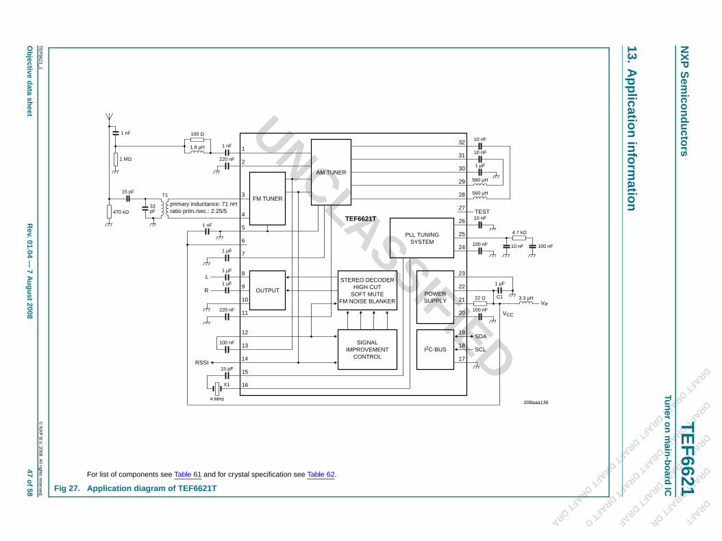
008aaa136
4.7 kΩ
3.3 µH
CC
VP
10 nF 100 nF
© N
XP
B.V. 2008. A
ll rights reserved.
UNCLASSIFIED
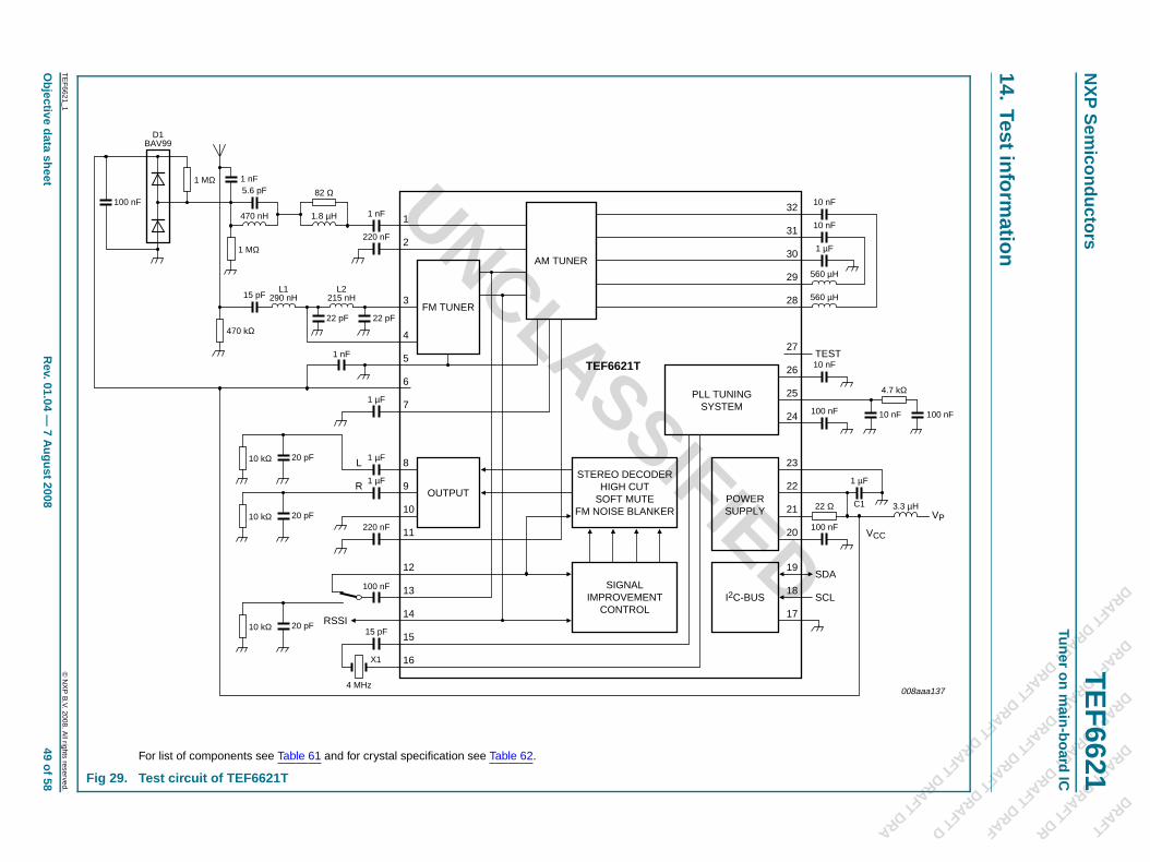
For list of components see Table 61 and for crystal specification see Table 62.
Fig 27. Application diagram of TEF6621T
100 nF
1 µF
100 nF
10 nF
10 nF
10 nF
15 pF
1 nF
15 pF
1 nF
220 nF
1 µF
1 µF
220 nF
1 µF
100 nF
X1
4 MHz
22 Ω
100 Ω
1 MΩ
470 kΩ
1 µF
RSSI
SCL
SDA
TEST
V
17
AM TUNER
FM TUNERprimary inductance: 71 nHratio prim./sec.: 2.25/5
OUTPUT
TEF6621T
560 µH
1.8 µH
T1
560 µH
PLL TUNINGSYSTEM
POWERSUPPLY
I2C-BUS
STEREO DECODERHIGH CUT
SOFT MUTEFM NOISE BLANKER
SIGNALIMPROVEMENT
CONTROL
18
19
20
21
22
23
29
28
27
30
31
321
2
5
6
7
11
12
13
14
15
16
24
25
26
10
9
8
R
L
4
3
33pF
1 nF
C1
xxxx xxxxxxxxxxxxxxxxxxxxxxxxxxxxxx x xxxxxxxxxxxxxx xxxxxxxxxx xxx xxxxxx xxxxxxxxxxxxxxxxxxxxxxx xxxxxxxxxxxxxxxxxxxxxxxxxxx xxxxxx xx xxxxxxxxxxxxxxxxxxxxxxxxxxxxx xxxxxxxxxxxxxxxxxxxxxx xxxxxxxxxxx xxxxxxx xxxxxxxxxxxxxxxxxxxxxxxxxxxxxxxxxxx xxxxxxxxxxxxxx xxxxxx xx xxxxxxxxxxxxxxxxxxxxxxxxxxxxxxxx xxxxxxxxxxxxxxxxxxxxxxxx xxxxxxxxxxxxxxxxxxxxxxxxxxxxxxxxxxxxxxxxxxxxxxxxxxxxx xxxxxxxxxxx xxxxx x x
TE
F6621_1
Objective data sheet
Rev. 01.04 —
7 August 2008
48 of 58
NX
P S
emicond
13
130 mm
DRAFT
DRAFT DRAFT DR
DRAFT DRAFT DRAFT DRAF
DRAFTDRAFT
DRAFTDRAFT
DRAFTD
DRAFT DRAFT DRAFT DRAFT DRAFT DRAFT DRA
uctorsT
EF
6621Tuner on m
ain-board IC
.1P
rinted-circuit board
, 35 µm)
001aah342
© N
XP
B.V. 2008. A
ll rights reserved.
UNCLASSIFIED
Fig 28. Printed-circuit board layout, suggested for application (this layout has been used in the NXP GH989 reference design
110 mm
xxxx xxxxxxxxxxxxxxxxxxxxxxxxxxxxxx x xxxxxxxxxxxxxx xxxxxxxxxx xxx xxxxxx xxxxxxxxxxxxxxxxxxxxxxx xxxxxxxxxxxxxxxxxxxxxxxxxxx xxxxxx xx xxxxxxxxxxxxxxxxxxxxxxxxxxxxx xxxxxxxxxxxxxxxxxxxxxx xxxxxxxxxxx xxxxxxx xxxxxxxxxxxxxxxxxxxxxxxxxxxxxxxxxxx xxxxxxxxxxxxxx xxxxxx xx xxxxxxxxxxxxxxxxxxxxxxxxxxxxxxxx xxxxxxxxxxxxxxxxxxxxxxxx xxxxxxxxxxxxxxxxxxxxxxxxxxxxxxxxxxxxxxxxxxxxxxxxxxxxx xxxxxxxxxxx xxxxx x x
TE
F6621_1
Objective data sheet
Rev. 01.04 —
7 August 2008
49 of 58
NX
P S
emicond
14.Test infor
1 nF1 MΩD1BAV99
DRAFT
DRAFT DRAFT DR
DRAFT DRAFT DRAFT DRAF
DRAFTDRAFT
DRAFTDRAFT
DRAFTD
DRAFT DRAFT DRAFT DRAFT DRAFT DRAFT DRA
uctorsT
EF
6621Tuner on m
ain-board IC
mation
008aaa137
100 nF
1 µF
100 nF
10 nF
10 nF
10 nF
22 Ω
4.7 kΩ
3.3 µH
SCL
SDA
TEST
VP
560 µH
560 µH
10 nF 100 nF
1 µF
VCC
C1
© N
XP
B.V. 2008. A
ll rights reserved.
UNCLASSIFIED
For list of components see Table 61 and for crystal specification see Table 62.
Fig 29. Test circuit of TEF6621T
15 pF
1 nF
15 pF
1 nF
5.6 pF
220 nF
1 µF
1 µF
220 nF
1 µF
100 nF
X1
4 MHz
82 Ω
1 MΩ
10 kΩ
470 kΩ
RSSI17
AM TUNER
FM TUNER
OUTPUT
TEF6621T
1.8 µH470 nH
L2215 nH
L1290 nH
PLL TUNINGSYSTEM
POWERSUPPLY
I2C-BUS
STEREO DECODERHIGH CUT
SOFT MUTEFM NOISE BLANKER
SIGNALIMPROVEMENT
CONTROL
18
19
20
21
22
23
29
28
27
30
31
321
2
5
6
7
11
12
13
14
15
16
24
25
26
10
9
8
R
L
4
3
22 pF
20 pF
10 kΩ 20 pF
10 kΩ 20 pF
22 pF
100 nF
DRAFT
DRAFT DRAFT DR
DRAFT DRAFT DRAF
RAF
DRAFTDRAFT
DRAF
FTD
DRAFT DRAFT DRAF
DRA
NXP Semiconductors TEF6621Tuner on main-board IC
T DT
DRAFTDRA
T DRAFT DRAFT DRAFT
UNCLASSIF
IED
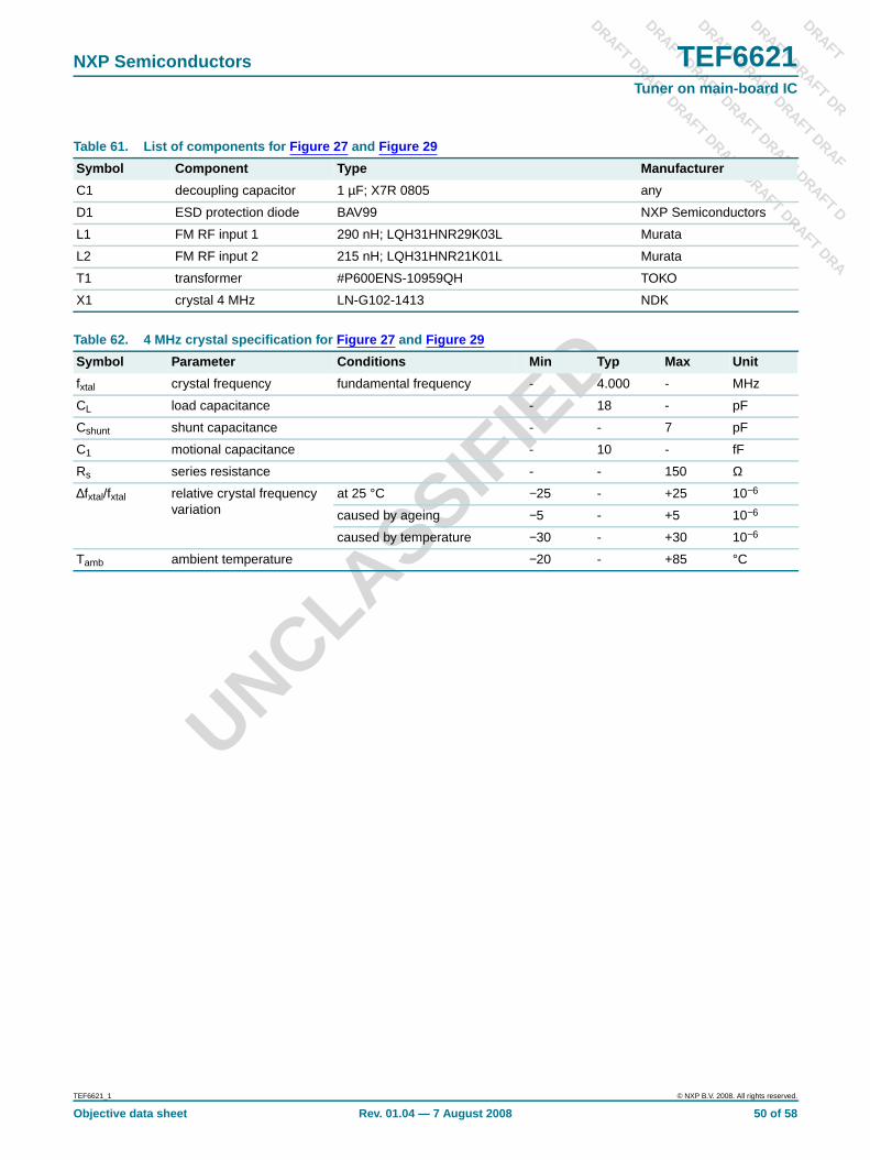
Table 61. List of components for Figure 27 and Figure 29
Symbol Component Type Manufacturer
C1 decoupling capacitor 1 µF; X7R 0805 any
D1 ESD protection diode BAV99 NXP Semiconductors
L1 FM RF input 1 290 nH; LQH31HNR29K03L Murata
L2 FM RF input 2 215 nH; LQH31HNR21K01L Murata
T1 transformer #P600ENS-10959QH TOKO
X1 crystal 4 MHz LN-G102-1413 NDK
Table 62. 4 MHz crystal specification for Figure 27 and Figure 29
Symbol Parameter Conditions Min Typ Max Unit
fxtal crystal frequency fundamental frequency - 4.000 - MHz
CL load capacitance - 18 - pF
Cshunt shunt capacitance - - 7 pF
C1 motional capacitance - 10 - fF
Rs series resistance - - 150 Ω
∆fxtal/fxtal relative crystal frequencyvariation
at 25 °C −25 - +25 10−6
caused by ageing −5 - +5 10−6
caused by temperature −30 - +30 10−6
Tamb ambient temperature −20 - +85 °C
TEF6621_1 © NXP B.V. 2008. All rights reserved.
Objective data sheet Rev. 01.04 — 7 August 2008 50 of 58
DRAFT
DRAFT DRAFT DR
DRAFT DRAFT DRAF
RAF
DRAFTDRAFT
DRAF
FTD
DRAFT DRAFT DRAF
DRA
NXP Semiconductors TEF6621Tuner on main-board IC
T DT
DRAFTDRA
T DRAFT DRAFT DRAFT
UNCLASSIF
IED
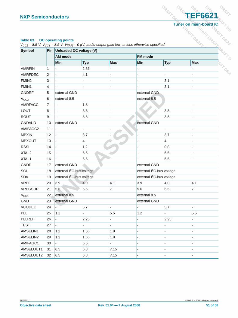
Table 63. DC operating pointsVCC2 = 8.5 V; VCC1 = 8.5 V; Vi(RF) = 0 µV; audio output gain low; unless otherwise specified.
Symbol Pin Unloaded DC voltage (V)
AM mode FM mode
Min Typ Max Min Typ Max
AMRFIN 1 - 2.85 - - - -
AMRFDEC 2 - 4.1 - - - -
FMIN2 3 - - - - 3.1 -
FMIN1 4 - - - - 3.1 -
GNDRF 5 external GND external GND
VCC2 6 external 8.5 external 8.5
AMRFAGC 7 - 1.8 - - - -
LOUT 8 - 3.8 - - 3.8 -
ROUT 9 - 3.8 - - 3.8 -
GNDAUD 10 external GND external GND
AMIFAGC2 11 - - - - - -
MPXIN 12 - 3.7 - - 3.7 -
MPXOUT 13 - 4 - - 4 -
RSSI 14 - 1.2 - - 0.8 -
XTAL2 15 - 6.5 - - 6.5 -
XTAL1 16 - 6.5 - - 6.5 -
GNDD 17 external GND external GND
SCL 18 external I2C-bus voltage external I2C-bus voltage
SDA 19 external I2C-bus voltage external I2C-bus voltage
VREF 20 3.9 4.0 4.1 3.9 4.0 4.1
VREGSUP 21 5.6 6.5 7 5.6 6.5 7
VCC1 22 external 8.5 external 8.5
GND 23 external GND external GND
VCODEC 24 - 5.7 - - 5.7 -
PLL 25 1.2 - 5.5 1.2 - 5.5
PLLREF 26 - 2.25 - - 2.25 -
TEST 27 - - - - - -
AMSELIN1 28 1.2 1.55 1.9 - - -
AMSELIN2 29 1.2 1.55 1.9 - - -
AMIFAGC1 30 - 5.5 - - - -
AMSELOUT1 31 6.5 6.8 7.15 - - -
AMSELOUT2 32 6.5 6.8 7.15 - - -
TEF6621_1 © NXP B.V. 2008. All rights reserved.
Objective data sheet Rev. 01.04 — 7 August 2008 51 of 58
DRAFT
DRAFT DRAFT DR
DRAFT DRAFT DRAF
RAF
DRAFTDRAFT
DRAF
FTD
DRAFT DRAFT DRAF
DRA
NXP Semiconductors TEF6621Tuner on main-board IC
T DT
DRAFTDRA
T DRAFT DRAFT DRAFT
UNCLASSIF
IED
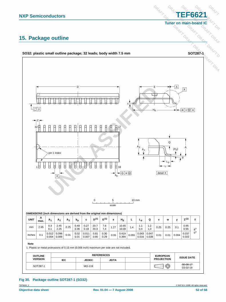
15. Package outline
Fig 30. Package outline SOT287-1 (SO32)
UNITA
max. A1 A2 A3 bp c D (1) E(1) e HE L L p Q Zywv θ
REFERENCESOUTLINEVERSION
EUROPEANPROJECTION ISSUE DATE
IEC JEDEC JEITA
mm
inches
2.65
0.1
0.25
0.01
1.4
0.055
0.30.1
2.452.25
0.490.36
0.270.18
20.720.3
7.67.4
1.2710.6510.00
1.21.0
0.950.55 8
0
o
o
0.25 0.1
0.004
0.25
DIMENSIONS (inch dimensions are derived from the original mm dimensions)
Note
1. Plastic or metal protrusions of 0.15 mm (0.006 inch) maximum per side are not included.
1.10.4
SOT287-1 MO-119
(1)
0.0120.004
0.0960.089
0.020.01
0.050.0470.039
0.4190.394
0.300.29
0.810.80
0.0110.007
0.0370.022
0.010.010.0430.016
w Mbp
D
HE
Z
e
c
v M A
XA
y
32 17
161
θ
AA1
A2
Lp
Q
detail X
L
(A )3
E
pin 1 index
0 5 10 mm
scale
SO32: plastic small outline package; 32 leads; body width 7.5 mm SOT287-1
00-08-1703-02-19
TEF6621_1 © NXP B.V. 2008. All rights reserved.
Objective data sheet Rev. 01.04 — 7 August 2008 52 of 58

DRAFT
DRAFT DRAFT DR
DRAFT DRAFT DRAF
RAF
DRAFTDRAFT
DRAF
FTD
DRAFT DRAFT DRAF
DRA
NXP Semiconductors TEF6621Tuner on main-board IC
T DT
DRAFTDRA
T DRAFT DRAFT DRAFT
UNCLASSIF
IED
16. Soldering of SMD packages
This text provides a very brief insight into a complex technology. A more in-depth accountof soldering ICs can be found in Application Note AN10365 “Surface mount reflowsoldering description”.
16.1 Introduction to solderingSoldering is one of the most common methods through which packages are attached toPrinted Circuit Boards (PCBs), to form electrical circuits. The soldered joint provides boththe mechanical and the electrical connection. There is no single soldering method that isideal for all IC packages. Wave soldering is often preferred when through-hole andSurface Mount Devices (SMDs) are mixed on one printed wiring board; however, it is notsuitable for fine pitch SMDs. Reflow soldering is ideal for the small pitches and highdensities that come with increased miniaturization.
16.2 Wave and reflow solderingWave soldering is a joining technology in which the joints are made by solder coming froma standing wave of liquid solder. The wave soldering process is suitable for the following:
• Through-hole components
• Leaded or leadless SMDs, which are glued to the surface of the printed circuit board
Not all SMDs can be wave soldered. Packages with solder balls, and some leadlesspackages which have solder lands underneath the body, cannot be wave soldered. Also,leaded SMDs with leads having a pitch smaller than ~0.6 mm cannot be wave soldered,due to an increased probability of bridging.
The reflow soldering process involves applying solder paste to a board, followed bycomponent placement and exposure to a temperature profile. Leaded packages,packages with solder balls, and leadless packages are all reflow solderable.
Key characteristics in both wave and reflow soldering are:
• Board specifications, including the board finish, solder masks and vias
• Package footprints, including solder thieves and orientation
• The moisture sensitivity level of the packages
• Package placement
• Inspection and repair
• Lead-free soldering versus SnPb soldering
16.3 Wave solderingKey characteristics in wave soldering are:
• Process issues, such as application of adhesive and flux, clinching of leads, boardtransport, the solder wave parameters, and the time during which components areexposed to the wave
• Solder bath specifications, including temperature and impurities
TEF6621_1 © NXP B.V. 2008. All rights reserved.
Objective data sheet Rev. 01.04 — 7 August 2008 53 of 58
DRAFT
DRAFT DRAFT DR
DRAFT DRAFT DRAF
RAF
DRAFTDRAFT
DRAF
FTD
DRAFT DRAFT DRAF
DRA
NXP Semiconductors TEF6621Tuner on main-board IC
T DT
DRAFTDRA
T DRAFT DRAFT DRAFT
UNCLASSIF
IED
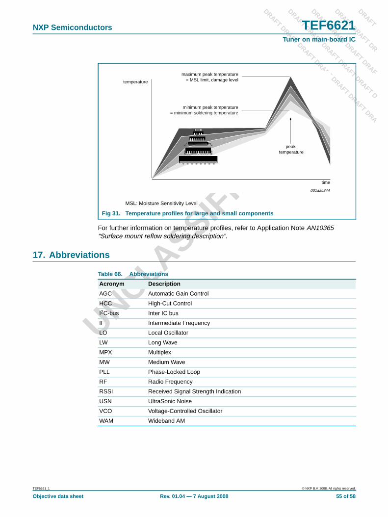
16.4 Reflow solderingKey characteristics in reflow soldering are:
• Lead-free versus SnPb soldering; note that a lead-free reflow process usually leads tohigher minimum peak temperatures (see Figure 31) than a SnPb process, thusreducing the process window
• Solder paste printing issues including smearing, release, and adjusting the processwindow for a mix of large and small components on one board
• Reflow temperature profile; this profile includes preheat, reflow (in which the board isheated to the peak temperature) and cooling down. It is imperative that the peaktemperature is high enough for the solder to make reliable solder joints (a solder pastecharacteristic). In addition, the peak temperature must be low enough that thepackages and/or boards are not damaged. The peak temperature of the packagedepends on package thickness and volume and is classified in accordance withTable 64 and 65
Moisture sensitivity precautions, as indicated on the packing, must be respected at alltimes.
Studies have shown that small packages reach higher temperatures during reflowsoldering, see Figure 31.
Table 64. SnPb eutectic process (from J-STD-020C)
Package thickness (mm) Package reflow temperature ( °C)
Volume (mm 3)
< 350 ≥ 350
< 2.5 235 220
≥ 2.5 220 220
Table 65. Lead-free process (from J-STD-020C)
Package thickness (mm) Package reflow temperature ( °C)
Volume (mm 3)
< 350 350 to 2000 > 2000
< 1.6 260 260 260
1.6 to 2.5 260 250 245
> 2.5 250 245 245
TEF6621_1 © NXP B.V. 2008. All rights reserved.
Objective data sheet Rev. 01.04 — 7 August 2008 54 of 58
DRAFT
DRAFT DRAFT DR
DRAFT DRAFT DRAF
RAF
DRAFTDRAFT
DRAF
FTD
DRAFT DRAFT DRAF
DRA
NXP Semiconductors TEF6621Tuner on main-board IC
T DT
DRAFTDRA
T DRAFT DRAFT DRAFT
UNCLASSIF
IED
For further information on temperature profiles, refer to Application Note AN10365“Surface mount reflow soldering description”.
17. Abbreviations
MSL: Moisture Sensitivity Level
Fig 31. Temperature profiles for large and small components
001aac844
temperature
time
minimum peak temperature= minimum soldering temperature
maximum peak temperature= MSL limit, damage level
peak temperature
Table 66. Abbreviations
Acronym Description
AGC Automatic Gain Control
HCC High-Cut Control
I2C-bus Inter IC bus
IF Intermediate Frequency
LO Local Oscillator
LW Long Wave
MPX Multiplex
MW Medium Wave
PLL Phase-Locked Loop
RF Radio Frequency
RSSI Received Signal Strength Indication
USN UltraSonic Noise
VCO Voltage-Controlled Oscillator
WAM Wideband AM
TEF6621_1 © NXP B.V. 2008. All rights reserved.
Objective data sheet Rev. 01.04 — 7 August 2008 55 of 58
DRAFT
DRAFT DRAFT DR
DRAFT DRAFT DRAF
RAF
DRAFTDRAFT
DRAF
FTD
DRAFT DRAFT DRAF
DRA
NXP Semiconductors TEF6621Tuner on main-board IC
T DT
DRAFTDRA
T DRAFT DRAFT DRAFT
UNCLASSIF
IED
18. Revision history
Table 67. Revision history
Document ID Release date Data sheet status Change notice Supersedes
TEF6621_1 yyyymmdd Objective data sheet - -
TEF6621_1 © NXP B.V. 2008. All rights reserved.
Objective data sheet Rev. 01.04 — 7 August 2008 56 of 58
DRAFT
DRAFT DRAFT DR
DRAFT DRAFT DRAF
RAF
DRAFTDRAFT
DRAF
FTD
DRAFT DRAFT DRAF
DRA
NXP Semiconductors TEF6621Tuner on main-board IC
T DT
DRAFTDRA
T DRAFT DRAFT DRAFT
UNCLASSIF
IED
19. Legal information
19.1 Data sheet status
[1] Please consult the most recently issued document before initiating or completing a design.
[2] The term ‘short data sheet’ is explained in section “Definitions”.
[3] The product status of device(s) described in this document may have changed since this document was published and may differ in case of multiple devices. The latest product statusinformation is available on the Internet at URL http://www.nxp.com.
19.2 Definitions
Draft — The document is a draft version only. The content is still underinternal review and subject to formal approval, which may result inmodifications or additions. NXP Semiconductors does not give anyrepresentations or warranties as to the accuracy or completeness ofinformation included herein and shall have no liability for the consequences ofuse of such information.
Short data sheet — A short data sheet is an extract from a full data sheetwith the same product type number(s) and title. A short data sheet is intendedfor quick reference only and should not be relied upon to contain detailed andfull information. For detailed and full information see the relevant full datasheet, which is available on request via the local NXP Semiconductors salesoffice. In case of any inconsistency or conflict with the short data sheet, thefull data sheet shall prevail.
19.3 Disclaimers
General — Information in this document is believed to be accurate andreliable. However, NXP Semiconductors does not give any representations orwarranties, expressed or implied, as to the accuracy or completeness of suchinformation and shall have no liability for the consequences of use of suchinformation.
Right to make changes — NXP Semiconductors reserves the right to makechanges to information published in this document, including withoutlimitation specifications and product descriptions, at any time and withoutnotice. This document supersedes and replaces all information supplied priorto the publication hereof.
Suitability for use — NXP Semiconductors products are not designed,authorized or warranted to be suitable for use in medical, military, aircraft,space or life support equipment, nor in applications where failure ormalfunction of an NXP Semiconductors product can reasonably be expectedto result in personal injury, death or severe property or environmental
damage. NXP Semiconductors accepts no liability for inclusion and/or use ofNXP Semiconductors products in such equipment or applications andtherefore such inclusion and/or use is at the customer’s own risk.
Applications — Applications that are described herein for any of theseproducts are for illustrative purposes only. NXP Semiconductors makes norepresentation or warranty that such applications will be suitable for thespecified use without further testing or modification.
Limiting values — Stress above one or more limiting values (as defined inthe Absolute Maximum Ratings System of IEC 60134) may cause permanentdamage to the device. Limiting values are stress ratings only and operation ofthe device at these or any other conditions above those given in theCharacteristics sections of this document is not implied. Exposure to limitingvalues for extended periods may affect device reliability.
Terms and conditions of sale — NXP Semiconductors products are soldsubject to the general terms and conditions of commercial sale, as publishedat http://www.nxp.com/profile/terms, including those pertaining to warranty,intellectual property rights infringement and limitation of liability, unlessexplicitly otherwise agreed to in writing by NXP Semiconductors. In case ofany inconsistency or conflict between information in this document and suchterms and conditions, the latter will prevail.
No offer to sell or license — Nothing in this document may be interpretedor construed as an offer to sell products that is open for acceptance or thegrant, conveyance or implication of any license under any copyrights, patentsor other industrial or intellectual property rights.
Quick reference data — The Quick reference data is an extract of theproduct data given in the Limiting values and Characteristics sections of thisdocument, and as such is not complete, exhaustive or legally binding.
19.4 TrademarksNotice: All referenced brands, product names, service names and trademarksare the property of their respective owners.
I2C-bus — logo is a trademark of NXP B.V.
20. Contact information
For more information, please visit: http://www .nxp.com
For sales office addresses, please send an email to: salesad [email protected]
Document status [1] [2] Product status [3] Definition
Objective [short] data sheet Development This document contains data from the objective specification for product development.
Preliminary [short] data sheet Qualification This document contains data from the preliminary specification.
Product [short] data sheet Production This document contains the product specification.
TEF6621_1 © NXP B.V. 2008. All rights reserved.
Objective data sheet Rev. 01.04 — 7 August 2008 57 of 58
DRAFT
DRAFT DRAFT DR
DRAFT DRAFT DRAF
RAF
DRAFTDRAFT
DRAF
FTD
DRAFT DRAFT DRAF
DRA
NXP Semiconductors TEF6621Tuner on main-board IC
T DT
DRAFTDRA
T DRAFT DRAFT DRAFT
UNCLASSIF
IED
21. Contents
1 General description . . . . . . . . . . . . . . . . . . . . . . 12 Features . . . . . . . . . . . . . . . . . . . . . . . . . . . . . . . 13 Quick reference data . . . . . . . . . . . . . . . . . . . . . 24 Ordering information . . . . . . . . . . . . . . . . . . . . . 25 Block diagram . . . . . . . . . . . . . . . . . . . . . . . . . . 36 Pinning information . . . . . . . . . . . . . . . . . . . . . . 46.1 Pinning . . . . . . . . . . . . . . . . . . . . . . . . . . . . . . . 46.2 Pin description . . . . . . . . . . . . . . . . . . . . . . . . . 47 Functional description . . . . . . . . . . . . . . . . . . . 57.1 FM tuner . . . . . . . . . . . . . . . . . . . . . . . . . . . . . . 57.2 AM tuner . . . . . . . . . . . . . . . . . . . . . . . . . . . . . . 57.3 PLL tuning system . . . . . . . . . . . . . . . . . . . . . . 57.4 FM stereo decoder . . . . . . . . . . . . . . . . . . . . . . 57.5 Weak signal processing and noise blanker. . . . 57.6 I2C-bus transceiver . . . . . . . . . . . . . . . . . . . . . . 68 I2C-bus protocol . . . . . . . . . . . . . . . . . . . . . . . . . 68.1 Read mode . . . . . . . . . . . . . . . . . . . . . . . . . . . . 68.1.1 Read mode: data byte STATUS . . . . . . . . . . . . 78.1.2 Read mode: data byte LEVEL . . . . . . . . . . . . . 78.1.3 Read mode: data byte USN_WAM . . . . . . . . . . 88.1.4 Read mode: data byte IFCOUNTER . . . . . . . . 88.2 Write mode . . . . . . . . . . . . . . . . . . . . . . . . . . . . 98.2.1 Mode and subaddress byte for write. . . . . . . . 108.2.2 Write mode: data byte TUNER0 . . . . . . . . . . . 228.2.3 Write mode: data byte TUNER1 . . . . . . . . . . . 228.2.4 Write mode: data byte TUNER2 . . . . . . . . . . . 238.2.5 Write mode: data byte RADIO . . . . . . . . . . . . 248.2.6 Write mode: data byte SOFTMUTE0 . . . . . . . 248.2.7 Write mode: data byte SOFTMUTE1 . . . . . . . 258.2.8 Write mode: data byte SOFTMUTE2_FM. . . . 278.2.9 Write mode: data byte SOFTMUTE2_AM . . . 298.2.10 Write mode: data byte HIGHCUT0 . . . . . . . . . 298.2.11 Write mode: data byte HIGHCUT1 . . . . . . . . . 308.2.12 Write mode: data byte HIGHCUT2 . . . . . . . . . 328.2.13 Write mode: data byte STEREO0. . . . . . . . . . 348.2.14 Write mode: data byte STEREO1. . . . . . . . . . 348.2.15 Write mode: data byte STEREO2. . . . . . . . . . 368.2.16 Write mode: data byte CONTROL . . . . . . . . . 378.2.17 Write mode: data byte LEVEL_OFFSET . . . . 388.2.18 Write mode: data byte AM_LNA . . . . . . . . . . . 389 Limiting values. . . . . . . . . . . . . . . . . . . . . . . . . 3910 Thermal characteristics. . . . . . . . . . . . . . . . . . 3911 Static characteristics. . . . . . . . . . . . . . . . . . . . 4012 Dynamic characteristics . . . . . . . . . . . . . . . . . 4013 Application information. . . . . . . . . . . . . . . . . . 47
13.1 Printed-circuit board . . . . . . . . . . . . . . . . . . . . 4814 Test information. . . . . . . . . . . . . . . . . . . . . . . . 4915 Package outline . . . . . . . . . . . . . . . . . . . . . . . . 5216 Soldering of SMD packages . . . . . . . . . . . . . . 5316.1 Introduction to soldering. . . . . . . . . . . . . . . . . 5316.2 Wave and reflow soldering . . . . . . . . . . . . . . . 5316.3 Wave soldering. . . . . . . . . . . . . . . . . . . . . . . . 5316.4 Reflow soldering. . . . . . . . . . . . . . . . . . . . . . . 5417 Abbreviations . . . . . . . . . . . . . . . . . . . . . . . . . 5518 Revision history . . . . . . . . . . . . . . . . . . . . . . . 5619 Legal information . . . . . . . . . . . . . . . . . . . . . . 5719.1 Data sheet status . . . . . . . . . . . . . . . . . . . . . . 5719.2 Definitions . . . . . . . . . . . . . . . . . . . . . . . . . . . 5719.3 Disclaimers. . . . . . . . . . . . . . . . . . . . . . . . . . . 5719.4 Trademarks . . . . . . . . . . . . . . . . . . . . . . . . . . 5720 Contact information . . . . . . . . . . . . . . . . . . . . 5721 Contents. . . . . . . . . . . . . . . . . . . . . . . . . . . . . . 58
© NXP B.V. 2008. All rights reserved.For more information, please visit: http://www.nxp.comFor sales office addresses, please send an email to: [email protected]
Date of release: 7 August 2008
Document identifier: TEF6621_1
Please be aware that important notices concerning this document and the product(s)described herein, have been included in section ‘Legal information’.