Embed Size (px)
Citation preview
DPA422-426 DPA-Switch Family
www.power.com June 2015
Highly Integrated DC-DC Converter ICs forPower over Ethernet & Telecom Applications
This Product is Covered by Patents and/or Pending Patent Applications.
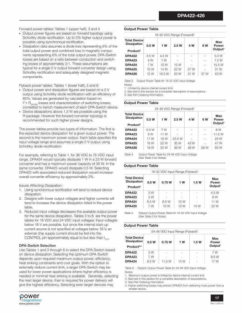
Output Power Table
36-75 VDC Input Range (Forward)2
Total DeviceDissipation3
Product4
0.5 W 1 W 2.5 W 4 W 6 WMax
Power Output1
DPA4227,8 7.5 W 10 W - - - 10 W
DPA423 12 W 16 W - - - 18 W
DPA424 16 W 23 W 35 W - - 35 W
DPA425 23 W 32 W 50 W 62 W - 70 W
DPA4265 25 W 35 W 55 W 70 W 83 W 100 W
36-75 VDC Input Range (Flyback)2
Total DeviceDissipation3
Product4
0.5 W 0.75 W 1 W 1.5 WMax
Power Output1
DPA4227,8 6.5 W 9.0 W - - 9.0 W
DPA423 9 W 13 W - - 13 W
DPA424 10 W 14.5 W 18 W 24 W 26 W
DPA425 -6 -6 -6 25.5 W 52 W
Table 1. Output Power Table. Notes: 1. Maximum output power is limited by device internal current limit. 2. See Applications Considerations section for complete description of assump-
tions, and for output powers with other input voltage ranges. 3. For device dissipation of 1.5 W or below, use P or G packages. Device
dissipation above 1.5 W is possible with R package. 4. Packages: P: DIP-8, G: SMD-8, R: TO-263-7C. For lead-free package options,
see Part Ordering Information. 5. Available in R package only. 6. Due to higher switching losses, the DPA425 may not deliver additional power
compared to a smaller device. 7. Available in P and G package only.8. DPA422 not recommended for new designs, use DPA423 instead.
Product Highlights
Highly Integrated Solution• Eliminates up to 50 external components–saves space, cost• Integrates 220 V high frequency MOSFET, PWM control• Lower cost plastic DIP surface mount (G package) and
through-hole (P package) options for designs ≤35 W• Thermally efficient TO-263-7C (R package) option for high
power applications
Superior Performance and Flexibility• Eliminates all external current sensing circuitry• Built-in auto-restart for output overload/open loop protection• Pin selectable 300/400 kHz fixed frequency• Wide input (line) voltage range: 16-75 VDC• Externally programmable current limit• Source connected tab reduces EMI• Line undervoltage (UV) detection: meets ETSI standards• Line overvoltage (OV) shutdown protection• UV/OV limits gate drive voltage for synchronous rectification• Fully integrated soft-start for minimum stress/overshoot• Supports forward or flyback topology• Cycle skipping: regulation to zero load without pre-load• Hysteretic thermal shutdown for automatic fault recovery• RoHS compliant P and G package options
EcoSmart™– Energy Efficient• Extremely low consumption at no-load• Cycle skipping at light load for high standby efficiency
Applications• PoE applications, VoIP phones, WLAN, security cameras• Telco central office equipment: xDSL, ISDN, PABX• Distributed power architectures (24 V/48 V bus)• Industrial controls
DescriptionThe DPA-Switch™ IC family is a highly integrated solution for DC-DC conversion applications with 16-75 VDC input.
DPA-Switch uses the same proven topology as TOPSwitch™, cost effectively integrating a power MOSFET, PWM control, fault protection and other control circuitry onto a single CMOS chip. High performance features are enabled with three user configurable pins. Hysteretic thermal shutdown is also provided. In addition, all critical parameters (i.e. current limit, frequency, PWM gain) have tight temperature and absolute tolerance, to simplify design and reduce system cost.
Figure 1. Typical Forward Converter Application.PI-2770-032002
D
S
C
DPA-SwitchVIN
VO
FX
L
CONTROL
SENSECIRCUIT
RESET/CLAMPCIRCUIT
Rev. U 06/15
2
DPA422-426
www.power.com
Section List
Functional Block Diagram ....................................................................................................................................... 3Pin Functional Description ...................................................................................................................................... 3DPA-Switch Family Functional Description ............................................................................................................ 4 CONTROL (C) Pin Operation .................................................................................................................................... 4 Oscillator and Switching Frequency .......................................................................................................................... 5 Pulse Width Modulator & Maximum Duty Cycle ........................................................................................................ 5 Minimum Duty Cycle and Cycle Skipping ................................................................................................................. 6 Error Amplifier .......................................................................................................................................................... 6 On-chip Current Limit with External Programmability ................................................................................................ 6 Line Undervoltage Detection (UV) ............................................................................................................................. 6 Line Overvoltage Shutdown (OV) .............................................................................................................................. 6 Line Feed-Forward with DCMAX Reduction ................................................................................................................ 6 Remote ON/OFF ...................................................................................................................................................... 7 Synchronization ........................................................................................................................................................ 7 Soft-Start ................................................................................................................................................................. 8 Shutdown/Auto-Restart ........................................................................................................................................... 8 Hysteretic Over-Temperature Protection ................................................................................................................... 8 Bandgap Reference ................................................................................................................................................. 8 High-Voltage Bias Current Source ............................................................................................................................ 8
Using Feature Pins ..................................................................................................................................................... 8 FREQUENCY (F) Pin Operation ................................................................................................................................ 8 LINE-SENSE (L) Pin Operation ................................................................................................................................. 9 EXTERNAL CURRENT LIMIT (X) Pin Operation ......................................................................................................... 9Typical Uses of FREQUENCY (F) Pin ...................................................................................................................... 11Typical Uses of LINE-SENSE (L) and EXTERNAL CURRENT LIMIT (X) Pins ....................................................... 11Application Examples .............................................................................................................................................. 14
Key Application Considerations .............................................................................................................................. 16 DPA-Switch Design Considerations ........................................................................................................................ 16 DPA-Switch Layout Considerations ........................................................................................................................ 18 Quick Design Checklist .......................................................................................................................................... 19 Design Tools .......................................................................................................................................................... 19
Product Specifications and Test Conditions ......................................................................................................... 20Typical Performance Characteristics .................................................................................................................. 27Package Outlines .................................................................................................................................................... 31Part Ordering Information ....................................................................................................................................... 32

Rev. U 06/15
3
DPA422-426
www.power.com
Figure 2. Functional Block Diagram.
Pin Functional Description
DRAIN (D) Pin:High-voltage power MOSFET drain output. The internal startup bias current is drawn from this pin through a switched high-voltage current source. Internal current limit sense point for drain current.
CONTROL (C) Pin:Error amplifier and feedback current input pin for duty cycle control. Internal shunt regulator connection to provide internal bias current during normal operation. It is also used as the connection point for the supply bypass and auto-restart/compensation capacitor.
LINE-SENSE (L) Pin:Input pin for overvoltage (OV), undervoltage (UV) lock out, line feed-forward with the maximum duty cycle (DCMAX) reduction, remote ON/OFF and synchronization. A connection to SOURCE pin disables all functions on this pin.
EXTERNAL CURRENT LIMIT (X) Pin:Input pin for external current limit adjustment and remote ON/OFF. A connection to SOURCE pin disables all functions on this pin.
FREQUENCY (F) Pin:Input pin for selecting switching frequency: 400 kHz if connected to SOURCE pin and 300 kHz if connected to CONTROL pin.
SOURCE (S) Pin:Output MOSFET source connection for the power return. Primary side control circuit common and reference point.
PI-2760-070501
SHUTDOWN/AUTO-RESTART
PWMCOMPARATOR
CLOCK
SAW300/400 kHz
CONTROLLEDTURN-ON
GATE DRIVER
CURRENT LIMITCOMPARATOR
INTERNAL UVCOMPARATOR
INTERNALSUPPLY
5.8 V4.8 V
SOURCE (S)
S
R
Q
DMAX
STOP SOFT-START
-
+
CONTROL (C)
LINE-SENSE (L)
EXTERNAL CURRENT LIMIT (X)
FREQUENCY (F)
-
+ 5.8 V
1 V
IFB
RE
ZC
VC
+
-
LEADINGEDGE
BLANKING
÷ 8
1
HYSTERETICTHERMAL
SHUTDOWN
SHUNT REGULATOR/ERROR AMPLIFIER +
-
DRAIN (D)
ON/OFF
SOFTSTART
DCMAX
VBG
DCMAX
VBG + VT
0
OV/UV
VI (LIMIT)CURRENT
LIMIT ADJUST
LINESENSE
SOFT START
CYCLE SKIPPING
STOP LOGIC
OSCILLATOR
Tab internally connected to SOURCE pin
(See layout considerations)
R Package(TO-263-7C)
1 2 3 4 5 7C L X S F D
F S
L
X
S
D
SC
4
2
3
1
P Package (DIP-8)G Package (SMD-8)
5
7
8
6
PI-4030-110507
Figure 2. Pin Configuration (Top View).

Rev. U 06/15
4
DPA422-426
www.power.com
Figure 4. Relationship of Duty Cycle to CONTROL Pin Current.
DPA-Switch Family Functional Description
DPA-Switch is an integrated switched mode power supply chip that converts a current at the control input to a duty cycle at the open drain output of a high-voltage power MOSFET. During normal operation the duty cycle of the power MOSFET decreases linearly with increasing CONTROL pin current as shown in Figure 4. A patented high-voltage CMOS technology allows both the high-voltage power MOSFET and all the low voltage control circuitry to be cost effectively integrated onto a single monolithic chip.
In addition to the standard TOPSwitch features, such as the high-voltage start-up, the cycle-by-cycle current limiting, loop compensation circuitry, auto-restart and thermal shutdown, DPA-Switch also offers many advanced features that reduce system cost and increase power supply performance and design flexibility. Following is a summary of the advanced features:
1. A fully integrated 5 ms soft-start limits peak currents and voltages during start-up and reduces or eliminates output overshoot in most applications.
2. A 75% maximum duty cycle (DCMAX) together with the line feed-forward with DCMAX reduction feature makes DPA-Switch well suited for both flyback and forward topologies.
3. High switching frequency (400 kHz/300 kHz, pin selectable) allows the use of smaller size transformers and offers high bandwidth for power supply control loop.
4. Cycle skipping operation at light load minimizes standby power consumption (typically <10 mA input current).
5. Line undervoltage ensures glitch free operations at both power-up and power-down and is tightly toleranced over process and temperature to meet system level requirements common in DC to DC converters (e.g. ETSI).
6. Line overvoltage protects DPA-Switch against excessive input voltage and line surge.
7. External current limit adjustment allows the setting of the current limit externally to a lower level near the operating peak current and, if desired, further adjusts the level gradu-ally as line voltage rises. This makes possible an ideal implementation of overload power limiting.
8. Synchronization function allows the synchronization of DPA-Switch operation to an external lower frequency.
9. Remote ON/OFF feature permits DPA-Switch based power supplies to be easily switched on/off using logic signals. Maximum input current consumption is 2 mA in remote OFF.
10. Hysteretic over-temperature shutdown provides automatic recovery from thermal fault.
11. Tight absolute tolerances and small temperature variations on switching frequency, current limit, and undervoltage lock out threshold (UV).
Three pins, LINE-SENSE (L), EXTERNAL CURRENT LIMIT (X) and FREQUENCY (F), are used to implement all the pin -controllable features. A resistor from the LINE-SENSE pin to DC input bus implements line UV, line OV and line feed-forward with DCMAX reduction. A resistor from the EXTERNAL CURRENT LIMIT pin to the SOURCE pin sets current limit externally. In
addition, remote ON/OFF may be implemented through either the LINE-SENSE pin or the EXTERNAL CURRENT LIMIT pin depending on the polarity of the logic signal available as well as other system specific considerations. Shorting both the LINE-SENSE and the EXTERNAL CURRENT LIMIT pins to the SOURCE pin disables line OV, line UV, line feed-forward with DCMAX reduction, external current limit, remote ON/OFF and synchronization. The FREQUENCY pin sets the switching frequency to 400 kHz if connected to the SOURCE pin, or 300 kHz if connected to the CONTROL pin. This pin should not be left open. Please refer to “Using Feature Pins” section for detailed information regarding the proper use of those pins.
CONTROL (C) Pin OperationThe CONTROL pin is a low impedance node that is capable of receiving a combined supply and feedback current. During normal operation, a shunt regulator is used to separate the feedback signal from the supply current. CONTROL pin voltage VC is the supply voltage for the control circuitry including the MOSFET gate driver. An external bypass capacitor closely connected between the CONTROL and SOURCE pins is required to supply the instantaneous gate drive current. The total amount of capacitance connected to this pin also sets the auto-restart timing as well as control loop compensation.
When the DC input voltage is applied to the DRAIN pin during start-up, the MOSFET is initially off, and the CONTROL pin capacitor is charged through the switched high-voltage current source connected internally between the DRAIN and CONTROL pins. When the CONTROL pin voltage VC reaches approximately 5.8 V, the control circuitry is activated and the soft-start begins. The soft-start circuit gradually increases the duty cycle of the MOSFET from zero to the maximum value over approximately 5 ms. The high-voltage current source is turned off at the end of the soft-start. If no external feedback/supply current is fed into the CONTROL pin by the end of the soft-start, the CONTROL pin will start discharging in response to the supply current drawn by the control circuitry and the gate current of the switching MOSFET driver. If the power supply is designed properly, and no fault condition such as open loop or
PI-2761-112102
Dut
y C
ycle
(%)
IC (mA)
IL = 115 µA
IL <
IL(DC)
IC
(SKIP)
Slope = PWM Gain
ICD1 IB
Auto-restart
75
4
42

Rev. U 06/15
5
DPA422-426
www.power.com
overloaded output exists, the feedback loop will close, providing external CONTROL pin current, before the CONTROL pin voltage has had a chance to discharge to the lower threshold voltage of approximately 4.8 V (internal supply undervoltage lockout threshold). When the externally fed current charges the CONTROL pin to the shunt regulator voltage of 5.8 V, current in excess of the consumption of the chip is shunted to SOURCE through resistor RE as shown in Figure 2. This current flowing through RE controls the duty cycle of the power MOSFET to provide closed loop regulation. The shunt regulator has a finite low output impedance ZC that sets the gain of the error amplifier when used in a primary feedback configuration. The dynamic impedance ZC of the CONTROL pin together with the external CONTROL pin capacitance sets the dominant pole for the control loop.
When a fault condition such as an open loop or overloaded output prevents the flow of an external current into the CONTROL pin, the capacitor on the CONTROL pin discharges towards 4.8 V. At 4.8 V auto-restart is activated which turns the output MOSFET off and puts the control circuitry in a low current standby mode. The high-voltage current source turns on and charges the external capacitance again. A hysteretic internal supply undervoltage comparator keeps VC within a window of typically 4.8 V to 5.8 V by turning the high-voltage current source on and off as shown in Figure 5. The auto-restart circuit has a divide-by-8 counter that prevents the output MOSFET from turning on again until eight discharge/charge cycles have elapsed. This is accomplished by enabling the output MOSFET only when the divide-by-8 counter reaches full count (S7). The counter effectively limits DPA-Switch power dissipation as well as the maximum power delivered to the power supply output by reducing the auto-restart duty cycle to typically 4%. Auto-restart mode continues until output voltage regulation is again achieved through closure of the feedback loop.
Oscillator and Switching FrequencyThe internal oscillator linearly charges and discharges an internal capacitance between two voltage levels to create a sawtooth waveform for the pulse width modulator. The oscillator sets both the pulse width modulator latch and the current limit latch at the beginning of each cycle.
The nominal switching frequency of 400 kHz was chosen to minimize the transformer size and to allow faster power supply loop response. The FREQUENCY pin, when shorted to the CONTROL pin, lowers the switching frequency to 300 kHz, which may be preferable in some applications such as those employing secondary synchronous rectification. Otherwise, the FREQUENCY pin should be connected to the SOURCE pin for the default 400 kHz.
Pulse Width Modulator and Maximum Duty CycleThe pulse width modulator implements voltage mode control by driving the output MOSFET with a duty cycle inversely proportional to the current into the CONTROL pin that is in excess of the internal supply current of the chip (see Figure 4). The excess current is the feedback error signal that appears across RE (see Figure 2). This signal is filtered by an RC network with a typical corner frequency of 30 kHz to reduce the effect of switching noise in the chip supply current generated by the MOSFET gate driver. The filtered error signal is compared with the internal oscillator sawtooth waveform to generate the duty cycle waveform. As the control current increases, the duty cycle decreases. A clock signal from the oscillator sets a latch that turns on the output MOSFET. The pulse width modulator resets the latch, turning off the output MOSFET. Note that a minimum current must be driven into the CONTROL pin before the duty cycle begins to change.
PI-3867-050602
S1 S2 S6 S7 S1 S2 S6 S7S0 S1 S7S0 S0 5.8 V4.8 V
S7
0 V
0 V
0 V
VLINE
VC
VDRAIN
VOUT
Note: S0 through S7 are the output states of the auto-restart counter
21 2 3 4
0 V
~ ~
~ ~
~ ~
~ ~
S6 S7
~ ~
~ ~
~ ~
VUV
~ ~
~ ~
~ ~
~ ~
S2~ ~
Figure 5. Typical Waveforms for (1) Power Up, (2) Normal Operation, (3) Auto-restart and (4) Power Down.

Rev. U 06/15
6
DPA422-426
www.power.com
The maximum duty cycle, DCMAX is set at a default maximum value of 75% (typical). However, by connecting the LINE-SENSE to the DC input bus through a resistor with appropriate value, the maximum duty cycle can be made to decrease from 75% to 33% (typical) as shown in Figure 7 when input line voltage increases (see Line Feed-Forward with DCMAX Reduction).
Minimum Duty Cycle and Cycle SkippingTo maintain power supply output regulation, the pulse width modulator reduces duty cycle as the load at the power supply output decreases. This reduction in duty cycle is proportional to the current flowing into the CONTROL pin. As the CONTROL pin current increases, the duty cycle reduces linearly towards a minimum value specified as minimum duty cycle, DCMIN. After reaching DCMIN, if CONTROL pin current is increased further by approximately 2 mA, the pulse width modulator will force the duty cycle from DCMIN to zero in a discrete step (refer to Figure 4). This feature allows a power supply to operate in a cycle skipping mode when the load consumes less power than the DPA-Switch delivers at minimum duty cycle, DCMIN. No additional control is needed for the transition between normal operation and cycle skipping. As the load increases or decreases, the power supply automatically switches between normal and cycle skipping mode as necessary.
Cycle skipping may be avoided, if so desired, by connecting a minimum load at the power supply output such that the duty cycle remains at a level higher than DCMIN at all times.
Error AmplifierThe shunt regulator can also perform the function of an error amplifier in primary side feedback applications. The shunt regulator voltage is accurately derived from a temperature-compensated bandgap reference. The gain of the error amplifier is set by the CONTROL pin dynamic impedance. The CONTROL pin clamps external circuit signals to the VC voltage level. The CONTROL pin current in excess of the supply current is separated by the shunt regulator and flows through RE as a voltage error signal.
On-chip Current Limit with External ProgrammabilityThe cycle-by-cycle peak drain current limit circuit uses the output MOSFET ON-resistance as a sense resistor. A current limit comparator compares the output MOSFET on-state drain to source voltage, VDS(ON) with a threshold voltage. At the current limit, VDS(ON) exceeds the threshold voltage and the MOSFET is turned off until the start of the next clock cycle. The current limit comparator threshold voltage is temperature compensated to minimize the variation of the current limit due to temperature related changes in RDS(ON) of the output MOSFET. The default current limit of DPA-Switch is preset internally. However, with a resistor connected between EXTERNAL CURRENT LIMIT pin and SOURCE pin, the current limit can be programmed externally to a lower level between 25% and 100% of the default current limit. Please refer to the graphs in the Typical Performance Characteristics section for the selection of the resistor value. By setting current limit low, a larger DPA-Switch than necessary for the power required can be used to take advantage of the lower RDS(ON) for higher efficiency/smaller heat sinking requirements. With a second resistor connected between the EXTERNAL CURRENT LIMIT pin and the DC input
bus, the current limit is reduced with increasing line voltage, allowing a true power limiting operation against line variation to be implemented in a flyback configuration.
The leading edge blanking circuit inhibits the current limit comparator for a short time after the output MOSFET is turned on. The leading edge blanking time has been set so that, if a power supply is designed properly, current spikes caused by primary-side capacitance and secondary-side rectifier reverse recovery time should not cause premature termination of the switching pulse.
The current limit after the leading edge blanking time is as shown in Figure 31. To avoid triggering the current limit in normal operation, the drain current waveform should stay within the envelope shown.
Line Undervoltage Detection (UV)At power up, UV keeps DPA-Switch off until the input line voltage reaches the under voltage upper threshold. At power down, UV holds DPA-Switch on until the input voltage falls below the under voltage lower threshold. A single resistor connected from the LINE-SENSE pin to the DC input bus sets UV upper and lower thresholds. To avoid false triggering by noise, a hysteresis is implemented which sets the UV lower threshold typically at 94% of the UV upper threshold. If the UV lower threshold is reached during operation without the power supply losing regulation and the condition stays longer than 10 µs (typical), the device will turn off and stay off until the UV upper threshold has been reached again. Then, a soft-start will be initiated the next time CONTROL pin voltage reaches 5.8.V. If the power supply loses regulation before reaching the UV lower threshold, the device will enter auto-restart. At the end of each auto-restart cycle (S7), the UV comparator is enabled. If the UV upper threshold is not exceeded, the MOSFET will be disabled during the next cycle (see Figure 5). The UV feature can be disabled independent of OV feature.
Line Overvoltage Shutdown (OV)The same resistor used for UV also sets an overvoltage threshold which, once exceeded, will force the DPA-Switch output into the off-state within one switching cycle. The ratio of OV and UV thresholds is preset at 2.7 as can be seen in Figure 7. When the MOSFET is off, the input voltage surge capability is increased to the voltage rating of the MOSFET (220 V), due to the absence of the reflected voltage and leakage spikes on the drain. A small amount of hysteresis is provided on the OV threshold to prevent noise triggering. The OV feature can be disabled independent of the UV feature as shown in Figure 13.
Line Feed-Forward with DCMAX ReductionThe same resistor used for UV and OV also implements line voltage feed-forward that minimizes output line ripple and reduces power supply output sensitivity to line transients. This feed-forward operation is illustrated in Figure 4 by the different values of IL. Note that for the same CONTROL pin current, higher line voltage results in smaller operating duty cycle. As an added feature, the maximum duty cycle DCMAX is also reduced from 75% (typical) at a voltage slightly higher than the UV threshold to 33% (typical) at the OV threshold (see Figures 4, 7). Limiting DCMAX at higher line voltages helps prevent transformer

Rev. U 06/15
7
DPA422-426
www.power.com
Figure 6. Synchronization Timing Diagram.
saturation due to large load transients in forward converter applications. DCMAX of 33% at the OV threshold was chosen to ensure that the power capability of the DPA-Switch is not restricted by this feature under normal operation.
Remote ON/OFFRemote ON/OFF control describes operation where the IC is turned on or off for long periods as opposed to the cycle-by- cycle on/off control, which is described in the Synchronization section below.
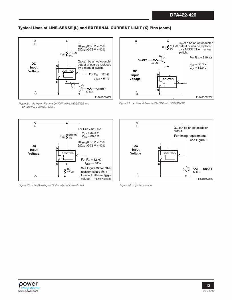
DPA-Switch can be turned on or off by controlling the current into the LINE-SENSE pin or out from the EXTERNAL CURRENT LIMIT pin (see Figure 7). This allows easy implementation of remote ON/OFF control of DPA-Switch in several different ways. A transistor or an optocoupler output connected between the EXTERNAL CURRENT LIMIT pin and the SOURCE pin implements this function with “active-on” (Figures 17, 19 and 21) while a transistor or an optocoupler output connected between the LINE-SENSE pin and the CONTROL pin implements the function with “active-off” (Figures 18, 20 and 22).
When a signal is received at the LINE-SENSE pin or the EXTERNAL CURRENT LIMIT pin to disable the output through any of the pin functions such as OV, UV and remote ON/OFF, DPA-Switch always completes its current switching cycle before the output is forced off. The internal oscillator is stopped at the end of the current cycle and stays there as long as the disable signal exists. When the signal at the above pins changes state from disable to enable, the internal oscillator starts the next switching cycle.
The remote ON/OFF feature can be used as a standby or power switch to turn off the DPA-Switch and keep it in a very low power consumption state for indefinitely long periods. If the
DPA-Switch is held in remote-off state for longer than 10 µs (typical), the CONTROL pin goes into the hysteretic mode of operation. In this mode, the CONTROL pin goes through alternate charge and discharge cycles between 4.8 V and 5.8 V (see CONTROL Pin Operation section above) and the IC runs entirely off the high-voltage DC input, but with very low power consumption (30 mW typical at 48 V with LINE-SENSE and EXTERNAL CURRENT LIMIT pins open). When the DPA-Switch is remotely turned on after entering this mode, it will initiate a normal start-up sequence with soft-start the next time the CONTROL pin reaches 5.8 V. In the worst case, the delay from remote on to start-up can be equal to the full discharge/charge cycle time of the CONTROL pin, which is approximately 36 ms for a 22 µF CONTROL pin capacitor. This reduced-consumption remote-off mode can eliminate expensive and unreliable in-line mechanical switches. It also allows for microprocessor-controlled turn-on and turn-off sequences that may be required in certain applications.
SynchronizationIn addition to sensing incoming current for OV, UV and remote ON/OFF, the LINE-SENSE pin also monitors its pin voltage through a 1 V threshold comparator. A pin voltage below 1 V turns on DPA-Switch. When the voltage at LINE-SENSE pin rises beyond 1 V to disable the output, DPA-Switch completes its current switching cycle before the output is forced off (similar to remote ON/OFF operation). The internal oscillator is stopped at the end of the current cycle awaiting the LINE-SENSE pin voltage to go low to start the next cycle. This allows the use of the 1 V threshold to synchronize DPA-Switch to an external signal with a frequency lower than its internal switching frequency. A transistor or an optocoupler output connected between the LINE-SENSE pin and the SOURCE pin implements this function (see Figure 24). Please refer to Figure 6 for the timing waveforms of synchronization operation.
PI-2762-070501
Oscillator(SAW)
DMAX
2 V
0 VVL
tON
fSYNC ≥ 128 kHz; tOFF £ 7.7 µs; 120 ns £ tON £ 2250 ns for fOSC = 400 kHz£ 3080 ns for fOSC = 300 kHz
tOFFON OFF SYNC
Time
Rev. U 06/15
8
DPA422-426
www.power.com
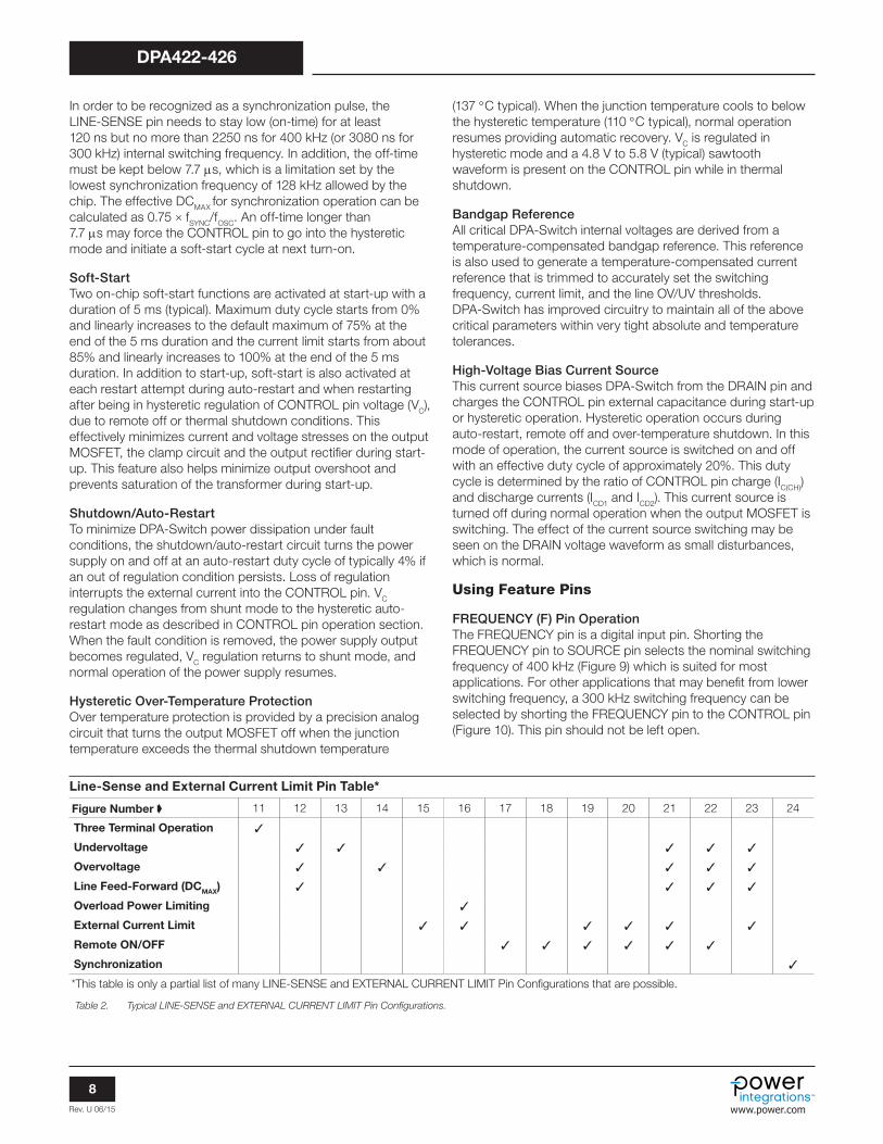
Table 2. Typical LINE-SENSE and EXTERNAL CURRENT LIMIT Pin Configurations.
In order to be recognized as a synchronization pulse, the LINE-SENSE pin needs to stay low (on-time) for at least 120 ns but no more than 2250 ns for 400 kHz (or 3080 ns for 300 kHz) internal switching frequency. In addition, the off-time must be kept below 7.7 µs, which is a limitation set by the lowest synchronization frequency of 128 kHz allowed by the chip. The effective DCMAX for synchronization operation can be calculated as 0.75 × fSYNC/fOSC. An off-time longer than 7.7 µs may force the CONTROL pin to go into the hysteretic mode and initiate a soft-start cycle at next turn-on.
Soft-StartTwo on-chip soft-start functions are activated at start-up with a duration of 5 ms (typical). Maximum duty cycle starts from 0% and linearly increases to the default maximum of 75% at the end of the 5 ms duration and the current limit starts from about 85% and linearly increases to 100% at the end of the 5 ms duration. In addition to start-up, soft-start is also activated at each restart attempt during auto-restart and when restarting after being in hysteretic regulation of CONTROL pin voltage (VC), due to remote off or thermal shutdown conditions. This effectively minimizes current and voltage stresses on the output MOSFET, the clamp circuit and the output rectifier during start-up. This feature also helps minimize output overshoot and prevents saturation of the transformer during start-up.
Shutdown/Auto-RestartTo minimize DPA-Switch power dissipation under fault conditions, the shutdown/auto-restart circuit turns the power supply on and off at an auto-restart duty cycle of typically 4% if an out of regulation condition persists. Loss of regulation interrupts the external current into the CONTROL pin. VC regulation changes from shunt mode to the hysteretic auto-restart mode as described in CONTROL pin operation section. When the fault condition is removed, the power supply output becomes regulated, VC regulation returns to shunt mode, and normal operation of the power supply resumes.
Hysteretic Over-Temperature ProtectionOver temperature protection is provided by a precision analog circuit that turns the output MOSFET off when the junction temperature exceeds the thermal shutdown temperature
(137 °C typical). When the junction temperature cools to below the hysteretic temperature (110 °C typical), normal operation resumes providing automatic recovery. VC is regulated in hysteretic mode and a 4.8 V to 5.8 V (typical) sawtooth waveform is present on the CONTROL pin while in thermal shutdown.
Bandgap ReferenceAll critical DPA-Switch internal voltages are derived from a temperature-compensated bandgap reference. This reference is also used to generate a temperature-compensated current reference that is trimmed to accurately set the switching frequency, current limit, and the line OV/UV thresholds. DPA-Switch has improved circuitry to maintain all of the above critical parameters within very tight absolute and temperature tolerances.
High-Voltage Bias Current SourceThis current source biases DPA-Switch from the DRAIN pin and charges the CONTROL pin external capacitance during start-up or hysteretic operation. Hysteretic operation occurs during auto-restart, remote off and over-temperature shutdown. In this mode of operation, the current source is switched on and off with an effective duty cycle of approximately 20%. This duty cycle is determined by the ratio of CONTROL pin charge (IC(CH)) and discharge currents (ICD1 and ICD2). This current source is turned off during normal operation when the output MOSFET is switching. The effect of the current source switching may be seen on the DRAIN voltage waveform as small disturbances, which is normal.
Using Feature Pins
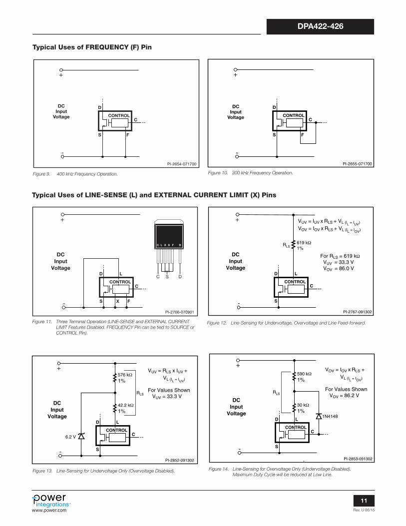
FREQUENCY (F) Pin OperationThe FREQUENCY pin is a digital input pin. Shorting the FREQUENCY pin to SOURCE pin selects the nominal switching frequency of 400 kHz (Figure 9) which is suited for most applications. For other applications that may benefit from lower switching frequency, a 300 kHz switching frequency can be selected by shorting the FREQUENCY pin to the CONTROL pin (Figure 10). This pin should not be left open.
Line-Sense and External Current Limit Pin Table*
Figure Number 11 12 13 14 15 16 17 18 19 20 21 22 23 24
Three Terminal Operation
Undervoltage
Overvoltage
Line Feed-Forward (DCMAX)
Overload Power Limiting
External Current Limit
Remote ON/OFF
Synchronization
*This table is only a partial list of many LINE-SENSE and EXTERNAL CURRENT LIMIT Pin Configurations that are possible.

Rev. U 06/15
9
DPA422-426
www.power.com
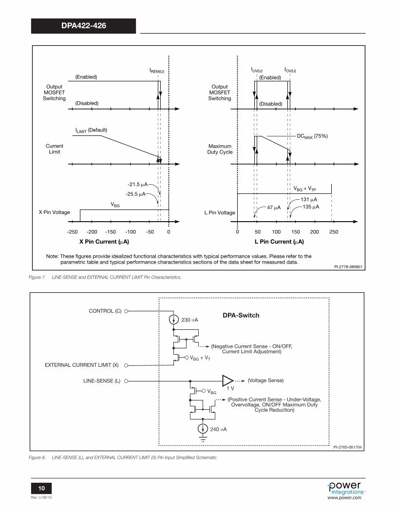
LINE-SENSE (L) Pin Operation When current is fed into the LINE-SENSE pin, it works as a voltage source of approximately 2.6 V up to a maximum current of +240 µA (typical). At +240 µA, this pin turns into a constant current sink. Refer to Figure 8. In addition, a comparator with a threshold of 1 V is connected at the pin and is used to detect when the pin is shorted to the SOURCE pin.
There are a total of five functions available through the use of the LINE-SENSE pin: OV, UV, line feed-forward with DCMAX reduction, remote ON/OFF and synchronization. Shorting the LINE-SENSE pin to the SOURCE pin disables all five functions. The LINE-SENSE pin is typically used for line sensing by connecting a resistor from this pin to the positive input DC voltage bus to implement OV, UV and line feed-forward with DCMAX reduction over line voltage. In this mode, the value of the resistor determines the line OV/UV thresholds, and the DCMAX is reduced linearly with input DC high-voltage starting from just above the UV threshold. This pin can also be used as the input pin for remote ON/OFF and synchronization. An external transistor placed between the LINE-SENSE pin and the CONTROL pin realizes remote ON/OFF via UV or OV threshold. Synchronization is available by connecting an open drain external MOSFET between the LINE-SENSE pin and the SOURCE pin to generate synchronization pulse. Each time the MOSFET turns on, the falling edge of the LINE-SENSE pin voltage initiates a new switching cycle. The lowest synchronization frequency guaranteed by DPA-Switch is 128 kHz. Refer to Table 2 for possible combinations of the functions with example circuits shown in Figure 11 through Figure 24. A description of specific functions in terms of the LINE-SENSE pin I/V characteristic is shown in Figure 7 (right hand side). The horizontal axis represents LINE-SENSE pin current with positive polarity indicating currents flowing into the pin. The meaning of the vertical axes varies with functions. For those that control the
on/off states of the output such as UV, OV and remote ON/OFF, the vertical axis represents the enable/disable states of the output. UV triggers at IUV (+50 µA typical with 4 µA hysteresis) and OV triggers at IOV (+135 µA typical with 4 µA hysteresis). Between the UV and OV thresholds, the output is enabled. For line feed-forward with DCMAX reduction, the vertical axis represents the magnitude of the DCMAX Line feed-forward with DCMAX reduction lowers maximum duty cycle from 75% at IL(DC) (+55 µA typical) to 33% at IOV (+135 µA).
EXTERNAL CURRENT LIMIT (X) Pin OperationWhen current is drawn out of the EXTERNAL CURRENT LIMIT pin, it works as a voltage source of approximately 1.3 V up to a maximum current of -230 µA (typical). At -230 µA, it turns into a constant current source (refer to Figure 8).
There are two functions available through the use of the EXTERNAL CURRENT LIMIT pin: external current limit and remote ON/OFF. Shorting the EXTERNAL CURRENT LIMIT pin and SOURCE pin disables both functions. In high efficiency applications, this pin can be used to reduce the current limit externally to a value close to the operating peak current, by connecting the pin to the SOURCE pin through a resistor. The pin can also be used as a remote ON/OFF control input. Table 2 shows several different ways of using this pin. See Figure 7 for a description of the functions where the horizontal axis (left hand side) represents the EXTERNAL CURRENT LIMIT pin current. The meaning of the vertical axes varies with function. For those that control the on/off states of the output such as remote ON/OFF, the vertical axis represents the enable/disable states of the output. For external current limit, the vertical axis represents the magnitude of the ILIMIT. Please see graphs in the Typical Performance Characteristics section for the current limit programming range and the selection of the appropriate resistor value.
Rev. U 06/15
10
DPA422-426
www.power.com
Figure 7. LINE-SENSE and EXTERNAL CURRENT LIMIT Pin Characteristics.
-250 -200 -150 -100 -50 50 100 150 200 2500 0
PI-2778-080801
OutputMOSFETSwitching
(Enabled)
(Disabled)
(Enabled)
(Disabled)
ILIMIT (Default)
CurrentLimit
VBG
-21.5 µA
-25.5 µAVBG + VTP
IUV(U)IREM(U) IOV(U)
X Pin Voltage
OutputMOSFETSwitching
MaximumDuty Cycle
L Pin Voltage
DCMAX (75%)
Note: These gures provide idealized functional characteristics with typical performance values. Please refer to the parametric table and typical performance characteristics sections of the data sheet for measured data.
X Pin Current (µA) L Pin Current (µA)
131 µA135 µA47 µA
VBG + VT
1 VVBG
230 ∝A
240 ∝A
CONTROL (C)
(Voltage Sense)
(Positive Current Sense - Under-Voltage,Overvoltage, ON/OFF Maximum Duty
Cycle Reduction)
(Negative Current Sense - ON/OFF,Current Limit Adjustment)
PI-2765-061704
DPA-Switch
LINE-SENSE (L)
EXTERNAL CURRENT LIMIT (X)
Figure 8. LINE-SENSE (L), and EXTERNAL CURRENT LIMIT (X) Pin Input Simplified Schematic
Rev. U 06/15
11
DPA422-426
www.power.com
Typical Uses of FREQUENCY (F) Pin
Typical Uses of LINE-SENSE (L) and EXTERNAL CURRENT LIMIT (X) Pins
Figure 9. 400 kHz Frequency Operation.
PI-2654-071700
DCInput
Voltage
+
-
D
S
CCONTROL
F
X F
PI-2766-070901
DCInput
Voltage
+
-
D
S
CCONTROL
LC S D
C L X S F D
Figure 11. Three Terminal Operation (LINE-SENSE and EXTERNAL CURRENT LIMIT Features Disabled. FREQUENCY Pin can be tied to SOURCE or CONTROL Pin).
Figure 13. Line-Sensing for Undervoltage Only (Overvoltage Disabled).
PI-2852-091302
DCInput
Voltage
+
-
D L
S
C
VUV = RLS x IUV + VL (IL = IUV) For Values Shown VUV = 33.3 V
RLS
6.2 V
576 k1%
42.2 k1%
CONTROL
Figure 14. Line-Sensing for Overvoltage Only (Undervoltage Disabled). Maximum Duty Cycle will be reduced at Low Line.
PI-2853-091302
DCInput
Voltage
+
-
D
S
CCONTROL
L
RLS
1N4148
VOV = IOV x RLS + VL (IL = IOV) For Values Shown VOV = 86.2 V
590 k1%
30 k1%
Figure 12. Line-Sensing for Undervoltage, Overvoltage and Line Feed-forward.
PI-2767-091302
DCInput
Voltage
+
-
D
S
CCONTROL
L
RLS619 k1%
VUV = IUV x RLS + VL (IL = IUV)
VOV = IOV x RLS + VL (IL = IOV)
For RLS = 619 k VUV = 33.3 V VOV = 86.0 V
Figure 10. 300 kHz Frequency Operation.
PI-2655-071700
DCInput
Voltage
+
-
D
S
CCONTROL
F

Rev. U 06/15
12
DPA422-426
www.power.com
Typical Uses of LINE-SENSE (L) and EXTERNAL CURRENT LIMIT (X) Pins (cont.)
Figure 15. Externally Set Current Limit. Figure 16. Current Limit Reduction with Line Voltage.
X
PI-2836-050602
DCInput
Voltage
+
-
D
S
C
RIL
For RIL = 12 k ILIMIT = 64%
See Figure 32 for other resistor values (RIL)
For RIL = 25 k ILIMIT = 34%
CONTROL
X
PI-2854-050602
DCInput
Voltage
+
-
D
S
C
363 kRLS
4.2 kRIL
100% @ 36 VDC64% @ 72 VDC
ILIMIT =ILIMIT =
CONTROL
Figure 17. Active-on (Fail Safe) Remote ON/OFF. Figure 18. Active-off Remote ON/OFF. Maximum Duty Cycle Will Be Reduced.
PI-2855-050602
DCInput
Voltage
+
-
D
S
CCONTROL
L
47 k
QR
RMC
37.4 k
QR can be an optocoupler output or can be replaced by a manual switch.
ON/OFF
X
PI-2625-040501
DCInput
Voltage
+
-
D
S
C
ON/OFF47 K
QR can be an optocoupler output or can be replaced by a manual switch.
QR
CONTROL
Figure 19. Active-on Remote ON/OFF with Externally Set Current Limit. Figure 20. Active-off Remote ON/OFF with Externally Set Current Limit.
X
ON/OFF
DCInput
Voltage
D
S
CCONTROL
PI-2857-050602
DCInput
Voltage
+
-
D
S
CCONTROL
L
47 k
QR
RMC
37.4 k
QR can be an optocoupler output or can be replaced by a manual switch.
ON/OFF
X
RIL
For RIL = 12 k ILIMIT = 64%
For RIL = 25 k ILIMIT = 34%
Rev. U 06/15
13
DPA422-426
www.power.com
Typical Uses of LINE-SENSE (L) and EXTERNAL CURRENT LIMIT (X) Pins (cont.)
DCInput
VoltageD
S
CCONTROL
L
ON/OFF
X
ON/OFF47 k
PI-2859-050602
DCInput
Voltage
+
-
D
S
CCONTROL
L
RIL
RLS
QR
619 k1%
DCMAX@36 V = 75%DCMAX@72 V = 42%
For RIL = 12 k ILIMIT = 64%
QR can be an optocoupler output or can be replaced by a manual switch.
Figure 21. Active-on Remote ON/OFF with LINE-SENSE and EXTERNAL CURRENT LIMIT.
Figure 22. Active-off Remote ON/OFF with LINE-SENSE.
Figure 23. Line-Sensing and Externally Set Current Limit.
PI-3868-050602
DCInput
Voltage
+
-
D
S
CCONTROL
L
ON/OFF47 kΩ
QR can be an optocoupler output.
QR
For timing requirements, see Figure 6.
Figure 24. Synchronization.
X
PI-2837-050602
DCInput
Voltage
+
-
D
S
CCONTROL
L
RIL
RLS
12 k
619 K1%
For RLS = 619 k
DCMAX@36 V = 75%DCMAX@72 V = 42%
For RIL = 12 k ILIMIT = 64%
See Figure 32 for other resistor values (RIL) to select different ILIMIT values
VUV = 33.3 V VOV = 86.0 V
Rev. U 06/15
14
DPA422-426
www.power.com
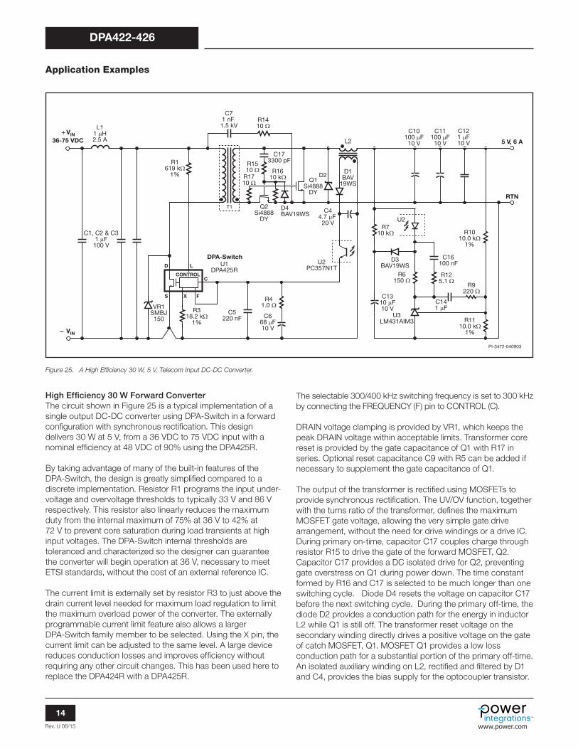
Figure 25. A High Efficiency 30 W, 5 V, Telecom Input DC-DC Converter.
U1DPA425R
D1BAV
19WSD2
C5220 nF
VR1SMBJ150 C6
68 µF10 V
C71 nF
1.5 kVR1410 Ω
T1
R318.2 kΩ
1%
R1619 kΩ
1%
R41.0 Ω
C10100 µF10 V
C11100 µF10 V
C121 µF10 V36-75 VDC
L11 µH2.5 A L2
C1, C2 & C31 µF
100 V
D L
S X F
CCONTROLCONTROL
U2PC357N1T
PI-3472-040903
DPA-Switch
5 V, 6 A
RTN
Q2Si4888
DY
R1510 Ω R16
10 kΩ
D4BAV19WS
R1710 Ω Q1
Si4888DY
C44.7 µF 20 V U2
D3BAV19WS
U3LM431AIM3
R9220 Ω
R1110.0 kΩ
1%
R1010.0 kΩ
1%
R125.1 Ω
R710 kΩ
C141 µF
C1310 µF10 V
C16100 nF
R6150 Ω
VIN+
VIN
C173300 pF
High Efficiency 30 W Forward ConverterThe circuit shown in Figure 25 is a typical implementation of a single output DC-DC converter using DPA-Switch in a forward configuration with synchronous rectification. This design delivers 30 W at 5 V, from a 36 VDC to 75 VDC input with a nominal efficiency at 48 VDC of 90% using the DPA425R.
By taking advantage of many of the built-in features of the DPA-Switch, the design is greatly simplified compared to a discrete implementation. Resistor R1 programs the input under-voltage and overvoltage thresholds to typically 33 V and 86 V respectively. This resistor also linearly reduces the maximum duty from the internal maximum of 75% at 36 V to 42% at 72 V to prevent core saturation during load transients at high input voltages. The DPA-Switch internal thresholds are toleranced and characterized so the designer can guarantee the converter will begin operation at 36 V, necessary to meet ETSI standards, without the cost of an external reference IC.
The current limit is externally set by resistor R3 to just above the drain current level needed for maximum load regulation to limit the maximum overload power of the converter. The externally programmable current limit feature also allows a larger DPA-Switch family member to be selected. Using the X pin, the current limit can be adjusted to the same level. A large device reduces conduction losses and improves efficiency without requiring any other circuit changes. This has been used here to replace the DPA424R with a DPA425R.
Application Examples
The selectable 300/400 kHz switching frequency is set to 300 kHz by connecting the FREQUENCY (F) pin to CONTROL (C).
DRAIN voltage clamping is provided by VR1, which keeps the peak DRAIN voltage within acceptable limits. Transformer core reset is provided by the gate capacitance of Q1 with R17 in series. Optional reset capacitance C9 with R5 can be added if necessary to supplement the gate capacitance of Q1.
The output of the transformer is rectified using MOSFETs to provide synchronous rectification. The UV/OV function, together with the turns ratio of the transformer, defines the maximum MOSFET gate voltage, allowing the very simple gate drive arrangement, without the need for drive windings or a drive IC. During primary on-time, capacitor C17 couples charge through resistor R15 to drive the gate of the forward MOSFET, Q2. Capacitor C17 provides a DC isolated drive for Q2, preventing gate overstress on Q1 during power down. The time constant formed by R16 and C17 is selected to be much longer than one switching cycle. Diode D4 resets the voltage on capacitor C17 before the next switching cycle. During the primary off-time, the diode D2 provides a conduction path for the energy in inductor L2 while Q1 is still off. The transformer reset voltage on the secondary winding directly drives a positive voltage on the gate of catch MOSFET, Q1. MOSFET Q1 provides a low loss conduction path for a substantial portion of the primary off-time. An isolated auxiliary winding on L2, rectified and filtered by D1 and C4, provides the bias supply for the optocoupler transistor.
Rev. U 06/15
15
DPA422-426
www.power.com
D
S
C
L
FX
CONTROL
DPA-Switch
C422 µF10 V
C30.1 µF50 V C10
0.33 µF
C110.1 µF
C81 µF50 V
C91 µF10 V
C7330 µF
6 V
L11 µH, 2A
C6330 µF
6 V
C5330 µF
6 V
C11 µF
100 V
C247 pF200 V
VR1SMAJ150A
R11 MΩ1%
R38.66 kΩ
1%
R45.1 Ω
R920 kΩ
1%
R834 kΩ
1%
R71 kΩ
R5100 Ω
R651 Ω
R2619 kΩ
1%
9, 101
2
3
6, 7
4
T1
5
U1DPA423G U2
PC357
U3CAT431L,
SOT23
D3BAV19, SOD323
D2SL43
+VIN36 - 57 VDC
J1-1
3.3 V, 2 A
J2-1
-VIN
J1-2
RTN
J2-2
PI-3806-061704
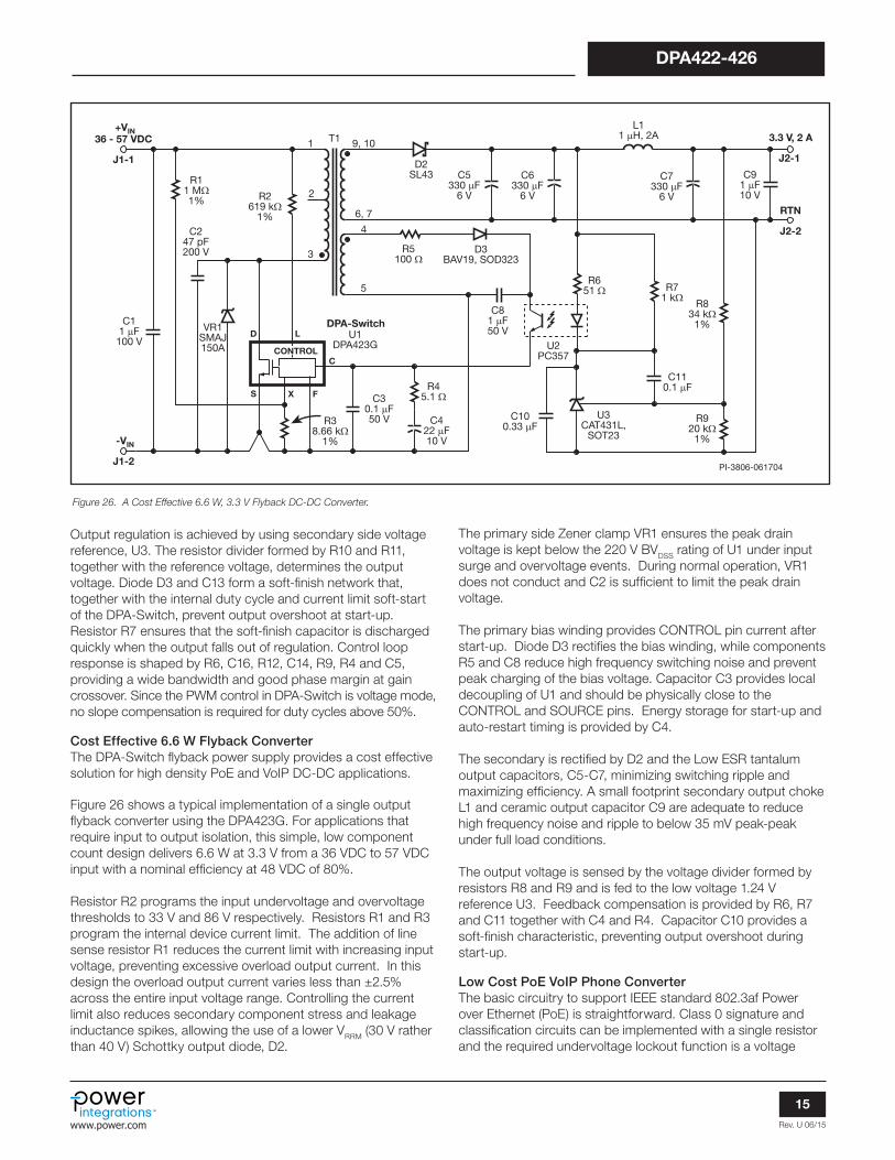
Figure 26. A Cost Effective 6.6 W, 3.3 V Flyback DC-DC Converter.
Output regulation is achieved by using secondary side voltage reference, U3. The resistor divider formed by R10 and R11, together with the reference voltage, determines the output voltage. Diode D3 and C13 form a soft-finish network that, together with the internal duty cycle and current limit soft-start of the DPA-Switch, prevent output overshoot at start-up. Resistor R7 ensures that the soft-finish capacitor is discharged quickly when the output falls out of regulation. Control loop response is shaped by R6, C16, R12, C14, R9, R4 and C5, providing a wide bandwidth and good phase margin at gain crossover. Since the PWM control in DPA-Switch is voltage mode, no slope compensation is required for duty cycles above 50%.
Cost Effective 6.6 W Flyback ConverterThe DPA-Switch flyback power supply provides a cost effective solution for high density PoE and VoIP DC-DC applications. Figure 26 shows a typical implementation of a single output flyback converter using the DPA423G. For applications that require input to output isolation, this simple, low component count design delivers 6.6 W at 3.3 V from a 36 VDC to 57 VDC input with a nominal efficiency at 48 VDC of 80%.
Resistor R2 programs the input undervoltage and overvoltage thresholds to 33 V and 86 V respectively. Resistors R1 and R3 program the internal device current limit. The addition of line sense resistor R1 reduces the current limit with increasing input voltage, preventing excessive overload output current. In this design the overload output current varies less than ±2.5% across the entire input voltage range. Controlling the current limit also reduces secondary component stress and leakage inductance spikes, allowing the use of a lower VRRM (30 V rather than 40 V) Schottky output diode, D2.
The primary side Zener clamp VR1 ensures the peak drain voltage is kept below the 220 V BVDSS rating of U1 under input surge and overvoltage events. During normal operation, VR1 does not conduct and C2 is sufficient to limit the peak drain voltage.
The primary bias winding provides CONTROL pin current after start-up. Diode D3 rectifies the bias winding, while components R5 and C8 reduce high frequency switching noise and prevent peak charging of the bias voltage. Capacitor C3 provides local decoupling of U1 and should be physically close to the CONTROL and SOURCE pins. Energy storage for start-up and auto-restart timing is provided by C4.
The secondary is rectified by D2 and the Low ESR tantalum output capacitors, C5-C7, minimizing switching ripple and maximizing efficiency. A small footprint secondary output choke L1 and ceramic output capacitor C9 are adequate to reduce high frequency noise and ripple to below 35 mV peak-peak under full load conditions.
The output voltage is sensed by the voltage divider formed by resistors R8 and R9 and is fed to the low voltage 1.24 V reference U3. Feedback compensation is provided by R6, R7 and C11 together with C4 and R4. Capacitor C10 provides a soft-finish characteristic, preventing output overshoot during start-up.
Low Cost PoE VoIP Phone ConverterThe basic circuitry to support IEEE standard 802.3af Power over Ethernet (PoE) is straightforward. Class 0 signature and classification circuits can be implemented with a single resistor and the required undervoltage lockout function is a voltage

Rev. U 06/15
16
DPA422-426
www.power.com
Figure 27. PoE Interface Circuit Using a Bipolar Transistor Pass-Switch and DPA424P.
U1DPA424PN
D6BAV
19WS
Q22Si4804
D21SL1315 V
Q21Si4804C2
1 µF 100 V
VR1SMAJ150 C5
47 µF10 V
D41BAV19WS
D3120CJQ060
R2110 Ω
R2210 Ω
R2310 kΩ
VR21
C212.2 nF
U2
T1
R1649 kΩ
1%
R31.0 Ω
C22-C24100 µF 5 V
VR416.8 V
D42IN4148
C31100 µF10 V
C414.7 µF, 35 V
C251 µF10 V
L11 µH 2.5 APoE Interface
L216 µH 4 A
C64.7 µF 20 V
D11BAV19WS
U3LM431AIM3
C112.2 µF10 V
R141 kΩ
R1510 kΩ
1%
R1610 kΩ
1%
R4160 Ω
R12150 Ω
R1311 Ω
C11 µF
100 V
U2PC357
N1T
R1110 kΩ
PI-3824-031008
DPA-Switch
5 V, 2.4 A
RTN
7.5 V, 0.4 A
20 V, 10 mA
C1368 nF
4
5
3
6
7
1 8
7 2
7
8
6
5
4 3Ethernet(RJ-45)
Connector
R213.3 kΩ
1%
R5220 kΩ
D101DL4002
DL4002D102
D103DL4002
DL4002D104
D105DL4002
DL4002D106
D107DL4002
DL4002D108
R2210 kΩ
R23174 k1%
R2110 k
R5124.9 kΩ
1% 1/4 W
D51BAV19
D52BAV19
C511 nF50 V
R5420 Ω
VR5128 V
(1,2)
(4,5)
(3,6)
(7,8)
D
S
C
L
FX
CONTROL
C12100 nF
R5320 kΩ
Q51TIP29C (100 V/1 A)
or MMBTA06
C4220 nF
Q20MMBTS3906
controlled pass-switch. By adding this circuitry to the front end of a DPA converter, a low cost and low component count PoE powered device (PD) power supply can be implemented. Figure 27 shows a typical PD solution.
The PoE specification requires the PD to provide three fundamental functions: discovery, classification, and pass-switch connection.
When input voltage is applied to the PD, it must present the correct discovery signature impedance in the voltage range of 2.5 VDC to 10 VDC. This impedance is provided by R51 in Figure 27.
The second “classification” phase occurs at input voltages 15 VDC to 20 VDC. The PD must draw a specified current to identify the device class (Class 0 specifies 0.5 mA to 4 mA). This is again accomplished by resistor R51.
In the third phase, the bipolar pass-switch (Q51 in Figure 27) connects the input voltage to the power supply at voltages above approximately 30 VDC (28 V+VR52). Zener diode VR51 conducts, driving the current through resistor R52 to the base of Q51. Resistor R53 prevents turn-on under other conditions. Once the Power supply has started, components D51, D52, C51 and R54 enhance the base-current drive by coupling power from the power supply bias winding.
Once the three start up phases have been successfully completed, the DPA-Switch is allowed to function as a forward converter (described in Figure 25 and accompanying text).
Key Application Considerations
DPA-Switch Design Considerations
Power TableThis section provides a description of the assumptions used to generate the power tables (Tables 1 and 3 through 6) and explains how to use the information provided by them.
All Power tables: Tables 1 and 3 through 6• Maximum output power is limited by the device internal
current limit. This is the peak output power which could become the continuous output power, provided adequate heat sinking is used.
• Data assumes adequate heat sinking to keep the junction temperature at or below 100 °C and worst case RDS(ON) at TJ = 100 °C.
• The use of P and G packages are recommended for device dissipation equal to or less than 1.5 W only due to package thermal limitation. For device dissipation above 1.5 W, use R package.
Rev. U 06/15
17
DPA422-426
www.power.com
Forward power tables: Tables 1 (upper half), 3 and 4• Output power figures are based on forward topology using
Schottky diode rectification. Up to 5% higher output power is possible using synchronous rectification.
• Dissipation data assumes a diode loss representing 6% of the total output power and combined loss in magnetic compo-nents representing 6% of the total output power. DPA-Switch losses are based on a ratio between conduction and switch-ing losses of approximately 3:1. These assumptions are typical for a single 5 V output forward converter design using Schottky rectification and adequately designed magnetic components.
Flyback power tables: Tables 1 (lower half), 5 and 6• Output power and dissipation figures are based on a 5 V
output using Schottky diode rectification with an efficiency of 85%. Values are generated by calculation based on I2 × RDS(ON) losses and characterization of switching losses, correlated to bench measurement of each DPA-Switch device.
• Device dissipations above 1.5 W are possible using the R package. However the forward converter topology is recommended for such higher power designs.
The power tables provide two types of information. The first is the expected device dissipation for a given output power. The second is the maximum power output. Each table specifies the input voltage range and assumes a single 5 V output using Schottky diode rectification.
For example, referring to Table 1, for 36 VDC to 75 VDC input range, DPA424 would typically dissipate 1 W in a 23 W forward converter and has a maximum power capacity of 35 W. In the same converter, DPA425 would dissipate 0.5 W. Selecting DPA425 with associated reduced dissipation would increase overall converter efficiency by approximately 2%.
Issues Affecting Dissipation: 1. Using synchronous rectification will tend to reduce device
dissipation. 2. Designs with lower output voltages and higher currents will
tend to increase the device dissipation listed in the power table.
3. Reduced input voltage decreases the available output power for the same device dissipation. Tables 3 to 6 are the power tables for 16 VDC and 24 VDC input voltages. Input voltages below 16 V are possible, but since the internal start-up current source is not specified at voltages below 16 V, an external chip supply current should be fed into the CONTROL pin approximately equal to but less than ICD1.
DPA-Switch SelectionUse Tables 1 and 3 through 6 to select the DPA-Switch based on device dissipation. Selecting the optimum DPA-Switch depends upon required maximum output power, efficiency, heat sinking constraints and cost goals. With the option to externally reduce current limit, a larger DPA-Switch may be used for lower power applications where higher efficiency is needed or minimal heat sinking is available. Generally, selecting the next larger device, than is required for power delivery will give the highest efficiency. Selecting even larger devices may
Output Power Table
16-32 VDC Range (Forward)2
Total Device Dissipation
Product3
0.5 W 1 W 2.5 W 4 W 6 WMax
Power Output1
DPA422 3.5 W 4.5 W - - - 5.0 WDPA423 5 W 7 W - - - 7.5 WDPA424 7 W 10 W 15 W - - 15.5 WDPA425 10 W 14 W 22 W 27 W - 31 WDPA426 12 W 16.5 W 25 W 31 W 37 W 43 W
Table 3. Output Power Table for 16-32 VDC Input Voltage. Notes: 1. Limited by device internal current limit. 2. See text in this section for a complete description of assumptions. 3. See Part Ordering Information.
Output Power Table
16-32 VDC Input Range (Flyback)2
Total DeviceDissipation
Product3
0.5 W 0.75 W 1 W 1.5 WMax
Power Output1
DPA422 3 W - - - 4.5 WDPA423 5 W - - - 6 WDPA424 6.5 W 8.5 W 10 W - 11 WDPA425 7 W 10 W 12 W 15 W 22 W
Output Power Table
24-48 VDC Range (Forward)2
Total Device Dissipation
Product3
0.5 W 1 W 2.5 W 4 W 6 WMax
Power Output1
DPA422 5.5 W 7 W - - - 8 WDPA423 8 W 11 W - - - 11.5 WDPA424 11 W 16 W 23.5 W - - 25 WDPA425 16 W 22 W 35 W 43 W - 47 WDPA426 18 W 25 W 39 W 48 W 58 W 65 W
Table 4. Output Power Table for 24-48 VDC Input Voltage (See Table 3 for Notes).
Table 5. Flyback Output Power Table for 16-32 VDC Input Voltage (See Table 3 for Notes).
Output Power Table
24-48 VDC Input Range (Flyback)2
Total DeviceDissipation
Product3,4
0.5 W 0.75 W 1 W 1.5 WMax
Power Output1
DPA422 3 W - - - 7 WDPA423 7 W - - - 8.5 WDPA424 8.5 W 11.5 W 14 W - 17 W
Table 6. Flyback Output Power Table for 24-48 VDC Input Voltage. Notes: 1. Maximum output power is limited by device internal current limit. 2. See text in this section for a complete description of assumptions. 3. See Part Ordering Information. 4. Higher switching losses may prevent DPA425 from delivering more power than a
smaller device.
Rev. U 06/15
18
DPA422-426
www.power.com
give little or no improvement in efficiency due to the improvement in conduction losses being negated by larger device switching losses. Figure 50 provides information on switching losses. This together with conduction loss calculations give an estimate of device dissipation.
Primary ClampA primary clamp network is recommended to keep the peak DRAIN voltage due to primary leakage inductance to below the BVDSS specification. A Zener diode combined with a small value capacitor connected across the primary winding is a low cost and low part count implementation.
Output RectificationRectification of the secondary is typically performed using Schottky diodes or synchronous rectification. Schottky diodes are selected for peak inverse voltage, output current, forward drop and thermal conditions. Synchronous rectification requires the additional complication of providing gate drive. The specified line undervoltage and line overvoltage thresholds of DPA-Switch simplifies deriving gate drive directly from the transformer secondary winding for many applications. The turns ratio of the transformer together with the under/over-voltage thresholds defines the minimum and maximum gate voltages, removing the need for Zeners to clamp the gate voltage.
Soft-StartGenerally a power supply experiences maximum stress at start-up before the feedback loop achieves regulation. For a period of 5 ms the on-chip soft-start linearly increases the duty cycle from zero to the default DCMAX at turn-on. In addition, the primary current limit increases from 85% to 100% over the same period. This causes the output voltage to rise in an orderly manner allowing time for the feedback loop to take control of the duty cycle. This integrated soft-start reduces the stress on the DPA-Switch MOSFET, clamp circuit and output diode(s), and helps prevent transformer saturation during start-up. Also, soft-start limits the amount of output voltage overshoot, and in many applications eliminates the need for a soft-finish capacitor. If necessary, to remove output overshoot, a soft-finish capacitor may be added to the secondary reference.
Switching FrequencyThe FREQUENCY pin of DPA-Switch offers a switching frequency option of 400 kHz or 300 kHz. Operating at 300 kHz will increase the amount of magnetization energy stored in the transformer. This is ideal for applications using synchronous rectification driven directly from the transformer secondary where this energy can be used to drive the catch MOSFET gate.
Transformer DesignIt is recommended that the forward converter transformer be designed for maximum operating flux swing of 1500 Gauss and a peak flux density of 3500 Gauss. When operating at the maximum current limit of the selected DPA-Switch (during overload conditions), neither magnetic component (transformer and output inductor) should be allowed to saturate. When a larger device than necessary has been selected, reducing the internal current limit close to the operating peak current limits
overload power and minimizes the size of the secondary components.
No-load and Standby ConsumptionCycle skipping operation at light or no-load can significantly reduce power loss. In addition this operating mode ensures that the output maintains regulation even without an external minimum load. However, if cycle skipping is undesirable in a particular application, it can be avoided by adding sufficient pre-load.
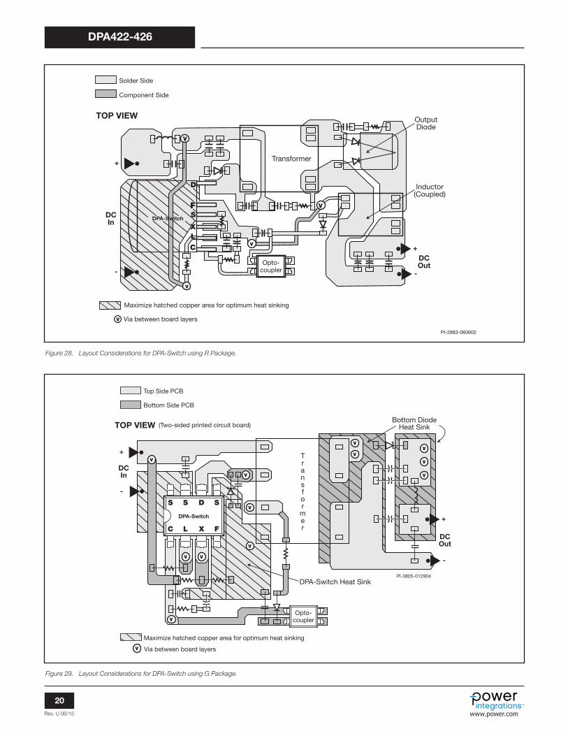
DPA-Switch Layout Considerations
The DPA-Switch can operate with large DRAIN current, the following guidelines should be carefully followed.
Primary Side ConnectionsThe tab of DPA-Switch R package is the intended return path for the high switching currents. Therefore, the tab should be connected by wide, low impedance traces back to the input decoupling capacitor. The SOURCE pin should not be used to return the power currents; incorrect operation of the device may result. The SOURCE is only intended as a signal ground. The device tab (SOURCE) is the correct connection for high current with the R package.
The CONTROL pin bypass capacitor should be located as close as possible to the SOURCE and CONTROL pins and its SOURCE connection trace should not be shared by the main MOSFET switching currents. All SOURCE pin referenced components connected to the LINE-SENSE or EXTERNAL CURRENT LIMIT pins should also be located closely between their respective pin and SOURCE. Once again, the SOURCE connection trace of these components should not be shared by the main MOSFET switching currents. It is critical that the tab (SOURCE) power switching currents are returned to the input capacitor through a separate trace that is not shared by the components connected to CONTROL, LINE-SENSE or EXTERNAL CURRENT LIMIT pins. Any traces to the L or X pins should be kept as short as possible and away from the DRAIN trace to prevent noise coupling. LINE-SENSE resistor (R1 in Figure 25) should be located close to the LINE-SENSE pin to minimize the trace length on the LINE-SENSE pin side.
In addition to the CONTROL pin capacitor (C6 in Figure 25), a high frequency bypass capacitor in parallel is recommended as close as possible between SOURCE and CONTROL pins for better noise immunity. The feedback optocoupler output should also be located close to the CONTROL and SOURCE pins of DPA-Switch.
Heat SinkingTo maximize heat sinking of the DPA-Switch R or G package and the other power components, special thermally conductive PC board material (aluminum clad PC board) is recommended. This has an aluminum sheet bonded to the PC board during the manufacturing process to provide heat sinking directly and allow the attachment of an external heat sink. If normal PC board material is used (such as FR4), providing copper areas on
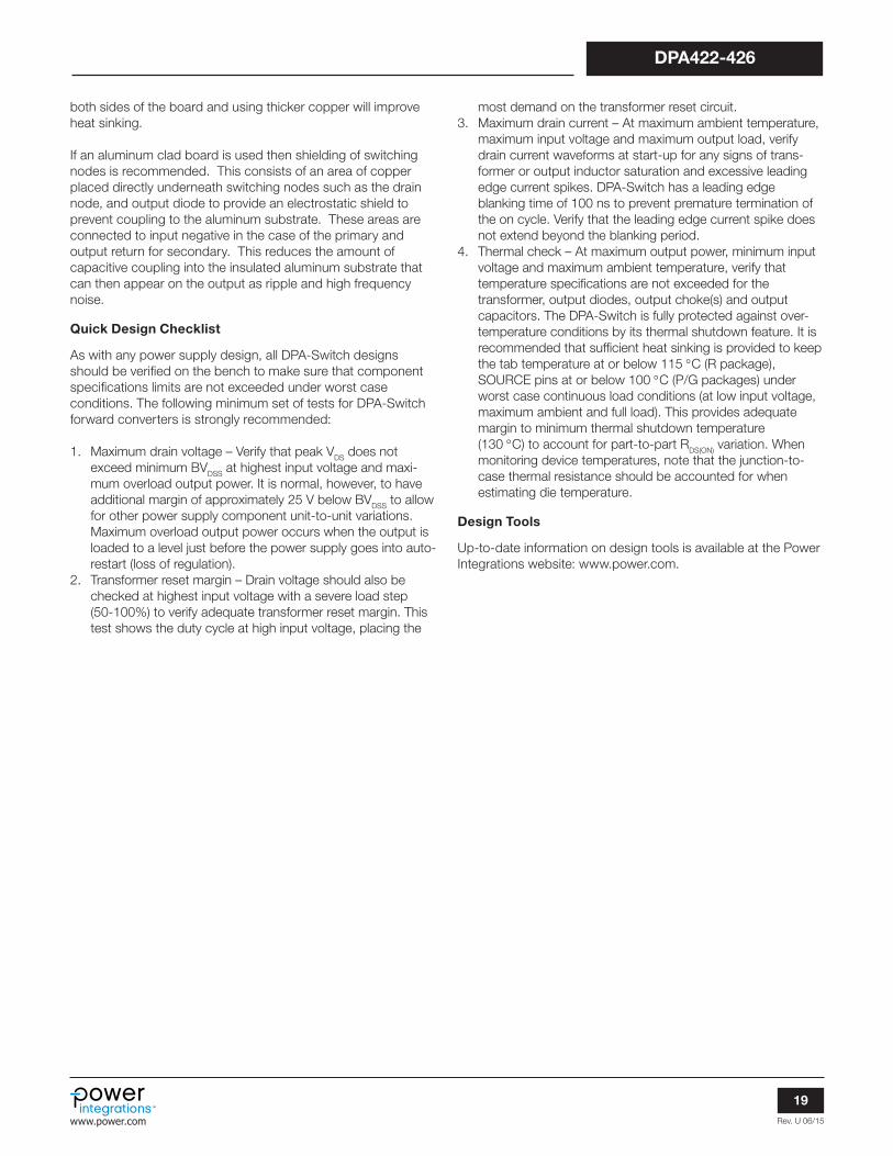
Rev. U 06/15
19
DPA422-426
www.power.com
both sides of the board and using thicker copper will improve heat sinking.
If an aluminum clad board is used then shielding of switching nodes is recommended. This consists of an area of copper placed directly underneath switching nodes such as the drain node, and output diode to provide an electrostatic shield to prevent coupling to the aluminum substrate. These areas are connected to input negative in the case of the primary and output return for secondary. This reduces the amount of capacitive coupling into the insulated aluminum substrate that can then appear on the output as ripple and high frequency noise.
Quick Design Checklist
As with any power supply design, all DPA-Switch designs should be verified on the bench to make sure that component specifications limits are not exceeded under worst case conditions. The following minimum set of tests for DPA-Switch forward converters is strongly recommended:
1. Maximum drain voltage – Verify that peak VDS does not exceed minimum BVDSS at highest input voltage and maxi-mum overload output power. It is normal, however, to have additional margin of approximately 25 V below BVDSS to allow for other power supply component unit-to-unit variations. Maximum overload output power occurs when the output is loaded to a level just before the power supply goes into auto-restart (loss of regulation).
2. Transformer reset margin – Drain voltage should also be checked at highest input voltage with a severe load step (50-100%) to verify adequate transformer reset margin. This test shows the duty cycle at high input voltage, placing the
most demand on the transformer reset circuit.3. Maximum drain current – At maximum ambient temperature,
maximum input voltage and maximum output load, verify drain current waveforms at start-up for any signs of trans-former or output inductor saturation and excessive leading edge current spikes. DPA-Switch has a leading edge blanking time of 100 ns to prevent premature termination of the on cycle. Verify that the leading edge current spike does not extend beyond the blanking period.
4. Thermal check – At maximum output power, minimum input voltage and maximum ambient temperature, verify that temperature specifications are not exceeded for the transformer, output diodes, output choke(s) and output capacitors. The DPA-Switch is fully protected against over-temperature conditions by its thermal shutdown feature. It is recommended that sufficient heat sinking is provided to keep the tab temperature at or below 115 °C (R package), SOURCE pins at or below 100 °C (P/G packages) under worst case continuous load conditions (at low input voltage, maximum ambient and full load). This provides adequate margin to minimum thermal shutdown temperature (130 °C) to account for part-to-part RDS(ON) variation. When monitoring device temperatures, note that the junction-to-case thermal resistance should be accounted for when estimating die temperature.
Design Tools
Up-to-date information on design tools is available at the Power Integrations website: www.power.com.
Rev. U 06/15
20
DPA422-426
www.power.com
V
V
PI-2883-060602
Solder Side
Component Side
TOP VIEW
S
L
C
X
Transformer
-
+
V+
-
DCOut
Maximize hatched copper area for optimum heat sinking
V Via between board layers
V
Opto-coupler
Inductor(Coupled)
OutputDiode
D
DPA-SwitchDCIn
PI-3805-012904
Transformer
Opto-coupler
+
DCOut
DCIn
+
-
V
V
V
V
V
V
V
V
V
V
DPA-Switch Heat Sink
Bottom DiodeHeat Sink
-
V V
C L X F
S D S
DPA-Switch
S
Top Side PCB
Bottom Side PCB
(Two-sided printed circuit board)TOP VIEW
Maximize hatched copper area for optimum heat sinking
Via between board layers
V
-
Figure 28. Layout Considerations for DPA-Switch using R Package.
Figure 29. Layout Considerations for DPA-Switch using G Package.

Rev. U 06/15
21
DPA422-426
www.power.com
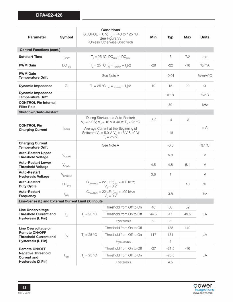
Parameter Symbol
Conditions SOURCE = 0 V; TJ = -40 to 125 °C
See Figure 33 (Unless Otherwise Specified)
Min Typ Max Units
Control Functions
Switching Frequency
fOSC TJ = 25 °C
FREQUENCY Pin Connected to SOURCE 375 400 425
kHzFREQUENCY Pin
Connected to CONTROL 282 300 317
Duty Cycle (Prior to Cycle Skipping)
DCMIN 4 6 %
Maximum Duty Cycle DCMAX IC = ICD1
VL = 0 V 71 75 79
%IL = 80 µA 52 62 71
IL = 115 µA 32 42 57
Control Current at Start of Cycle Skipping
IC(SKIP) TJ = 25 °C; fOSC = 400 kHz
DPA422 6.3 8.0
mA
DPA423 7.2 9.0
DPA424 8.2 10.0
DPA425 10.0 12.0
DPA426 11.5 14.0
External Bias Current
IB TJ = 25 °C; fOSC = 400 kHz
DPA422 1.8 2.5 3.1
mA
DPA423 2 2.8 3.5
DPA424 2.5 3.5 4.4
DPA425 3.6 4.8 6.0
DPA426 4.4 5.7 7.1
Absolute Maximum Ratings(1,4)
DRAIN Voltage ....................................................-0.3 V to 220 V DRAIN Peak Current: DPA422......................................1.31 A DPA423......................................1.75 A DPA424....................................... 3.5 A DPA425...........................................7 A DPA426....................................... 9.6 A CONTROL Voltage .................................................-0.3 V to 9 V CONTROL Current .........................................................100 mA LINE SENSE Pin Voltage ........................................ -0.3 V to 9 V EXTERNAL CURRENT LIMIT Pin Voltage ............... -0.3 V to 9 V FREQUENCY Pin Voltage ....................................... -0.3 V to 9 V
Storage Temperature ....................................... -65 °C to 150 °C Operating Junction Temperature(2) .................... -40 °C to 150 °C Lead Temperature(3) ....................................................... 260 °C Notes: 1. All voltages referenced to SOURCE, TA = 25 °C. 2. Normally limited by internal circuitry. 3. 1/16” from case for 5 seconds. 4. Maximum ratings specified may be applied, one at a time, without causing permanent damage to the product. Exposure to Absolute Maximum Rating conditions for extended periods of time may affect product reliability.
Thermal Resistance
Thermal Resistance: P or G Package: (qJA) ................................70 °C/W(1); 60 °C/W(2)
(qJC)(3) ..................................................11 °C/W R Package: (qJA) .................................................. 40 °C/W(4) (qJA) .................................................. 30 °C/W(5) (qJC)(6) ....................................................2 °C/W
Notes: 1. Soldered to 0.36 sq. in. (232 mm2), 2 oz. (610 g/m2) copper clad. 2. Soldered to 1 sq. in. (645 mm2), 2 oz. (610 g/m2) copper clad. 3. Measured on pin 7 (SOURCE) close to plastic interface. 4. Soldered to 1 sq. in. (645 mm2), 2 oz. (610 g/m2) copper clad. 5. Soldered to 3 sq. in. (1935 mm2), 2 oz. (610 g/m2) copper clad. 6. Measured at the back surface of tab.
Rev. U 06/15
22
DPA422-426
www.power.com
Parameter Symbol
Conditions SOURCE = 0 V; TJ = -40 to 125 °C
See Figure 33 (Unless Otherwise Specified)
Min Typ Max Units
Control Functions (cont.)
Softstart Time tSOFT TJ = 25 °C; DCMIN to DCMAX 5 7.2 ms
PWM Gain DCREG TJ = 25 °C; IC = IC(SKIP) + IB)/2 -28 -22 -18 %/mA
PWM Gain Temperature Drift See Note A -0.01 %/mA/°C
Dynamic Impedance ZC TJ = 25 °C; IC = IC(SKIP) + IB)/2 10 15 22 W
Dynamic Impedance Temperature Drift
0.18 %/°C
CONTROL Pin Internal Filter Pole
30 kHz
Shutdown/Auto-Restart
CONTROL Pin Charging Current
IC(CH))
During Startup and Auto-Restart: VC = 5.0 V; VD = 16 V & 40 V; TJ = 25 °C
-5.2 -4 -3
mAAverage Current at the Beginning of Softstart: VC = 5.0 V; VD = 16 V & 40 V;
TJ = 25 °C-19
Charging Current Temperature Drift
See Note A -0.6 %/ °C
Auto-Restart Upper Threshold Voltage
VC(AR)U 5.8 V
Auto-Restart Lower Threshold Voltage
VC(AR)L 4.5 4.8 5.1 V
Auto-Restart Hysteresis Voltage
VC(AR)Hyst 0.8 1 V
Auto-Restart Duty Cycle
DC(AR)
CCONTROL = 22 µF; fOSC = 400 kHz; VX = 0 V
10 %
Auto-Restart Frequency
f(AR)
CCONTROL = 22 µF; fOSC = 400 kHz; VX = 0 V
3.8 Hz
Line-Sense (L) and External Current Limit (X) Inputs
Line Undervoltage Threshold Current and Hysteresis (L Pin)
IUV TJ = 25 °C
Threshold from Off to On 48 50 52
µAThreshold from On to Off 44.5 47 49.5
Hysteresis 2 3
Line Overvoltage or Remote ON/OFF Threshold Current and Hysteresis (L Pin)
IOV TJ = 25 °C
Threshold from On to Off 135 149
µAThreshold from Off to On 117 131
Hysteresis 4
Remote ON/OFF Negative Threshold Current and Hysteresis (X Pin)
IREM TJ = 25 °C
Threshold from On to Off -27 -21.5 -16
µAThreshold from Off to On -25.5
Hysteresis 4.5
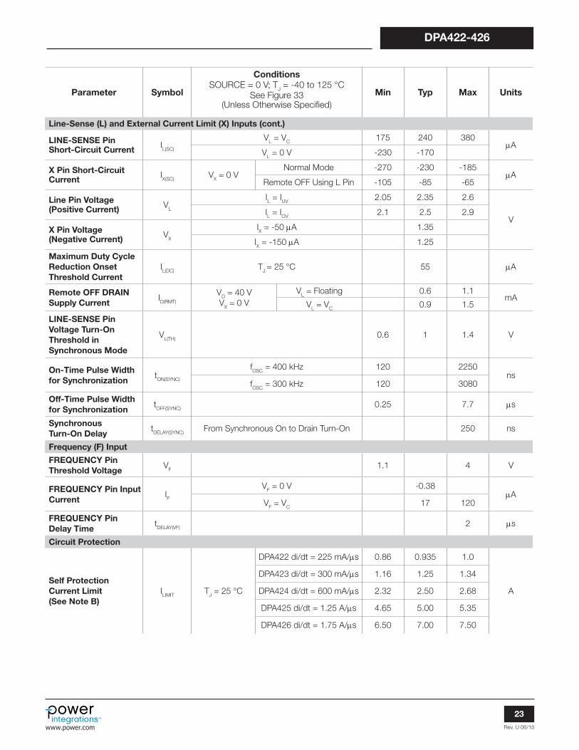
Rev. U 06/15
23
DPA422-426
www.power.com
Parameter Symbol
Conditions SOURCE = 0 V; TJ = -40 to 125 °C
See Figure 33 (Unless Otherwise Specified)
Min Typ Max Units
Line-Sense (L) and External Current Limit (X) Inputs (cont.)
LINE-SENSE Pin Short-Circuit Current IL(SC)
VL = VC 175 240 380µA
VL = 0 V -230 -170
X Pin Short-Circuit Current IX(SC) VX = 0 V
Normal Mode -270 -230 -185µA
Remote OFF Using L Pin -105 -85 -65
Line Pin Voltage (Positive Current) VL
IL = IUV 2.05 2.35 2.6
VIL = IOV 2.1 2.5 2.9
X Pin Voltage (Negative Current) VX
IX = -50 µA 1.35
IX = -150 µA 1.25
Maximum Duty Cycle Reduction Onset Threshold Current
IL(DC) TJ = 25 °C 55 µA
Remote OFF DRAIN Supply Current
ID(RMT)
VD = 40 V VX = 0 V
VL = Floating 0.6 1.1mA
VL = VC 0.9 1.5
LINE-SENSE Pin Voltage Turn-On Threshold in Synchronous Mode
VL(TH) 0.6 1 1.4 V
On-Time Pulse Width for Synchronization
tON(SYNC)
fOSC = 400 kHz 120 2250ns
fOSC = 300 kHz 120 3080
Off-Time Pulse Width for Synchronization
tOFF(SYNC) 0.25 7.7 µs
Synchronous Turn-On Delay
tDELAY(SYNC) From Synchronous On to Drain Turn-On 250 ns
Frequency (F) Input
FREQUENCY Pin Threshold Voltage
VF 1.1 4 V
FREQUENCY Pin Input Current
IFVF = 0 V -0.38
µAVF = VC 17 120
FREQUENCY Pin Delay Time
tDELAY(VF) 2 µs
Circuit Protection
Self Protection Current Limit (See Note B)
ILIMIT TJ = 25 °C
DPA422 di/dt = 225 mA/µs 0.86 0.935 1.0
A
DPA423 di/dt = 300 mA/µs 1.16 1.25 1.34
DPA424 di/dt = 600 mA/µs 2.32 2.50 2.68
DPA425 di/dt = 1.25 A/µs 4.65 5.00 5.35
DPA426 di/dt = 1.75 A/µs 6.50 7.00 7.50
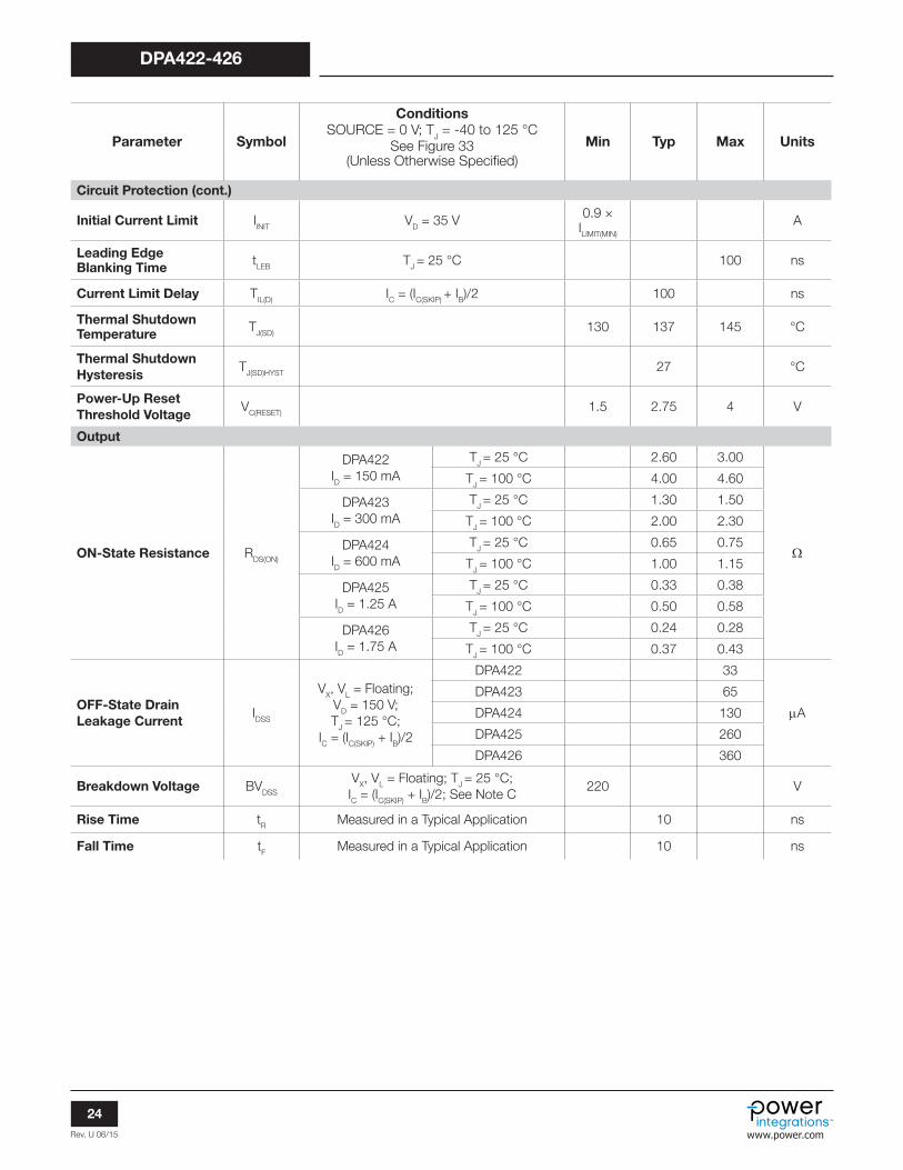
Rev. U 06/15
24
DPA422-426
www.power.com
Parameter Symbol
Conditions SOURCE = 0 V; TJ = -40 to 125 °C
See Figure 33 (Unless Otherwise Specified)
Min Typ Max Units
Circuit Protection (cont.)
Initial Current Limit IINIT VD = 35 V 0.9 × ILIMIT(MIN)
A
Leading Edge Blanking Time tLEB TJ = 25 °C 100 ns
Current Limit Delay TIL(D) IC = (IC(SKIP) + IB)/2 100 ns
Thermal Shutdown Temperature TJ(SD) 130 137 145 °C
Thermal Shutdown Hysteresis
TJ(SD)HYST 27 °C
Power-Up Reset Threshold Voltage
VC(RESET) 1.5 2.75 4 V
Output
ON-State Resistance RDS(ON)
DPA422 ID = 150 mA
TJ = 25 °C 2.60 3.00
W
TJ = 100 °C 4.00 4.60
DPA423 ID = 300 mA
TJ = 25 °C 1.30 1.50
TJ = 100 °C 2.00 2.30
DPA424 ID = 600 mA
TJ = 25 °C 0.65 0.75
TJ = 100 °C 1.00 1.15
DPA425 ID = 1.25 A
TJ = 25 °C 0.33 0.38
TJ = 100 °C 0.50 0.58
DPA426 ID = 1.75 A
TJ = 25 °C 0.24 0.28
TJ = 100 °C 0.37 0.43
OFF-State Drain Leakage Current
IDSS
VX, VL = Floating; VD = 150 V; TJ = 125 °C;
IC = (IC(SKIP) + IB)/2
DPA422 33
µA
DPA423 65
DPA424 130
DPA425 260
DPA426 360
Breakdown Voltage BVDSS
VX, VL = Floating; TJ = 25 °C; IC = (IC(SKIP) + IB)/2; See Note C
220 V
Rise Time tR Measured in a Typical Application 10 ns
Fall Time tF Measured in a Typical Application 10 ns

Rev. U 06/15
25
DPA422-426
www.power.com
Parameter Symbol
Conditions SOURCE = 0 V; TJ = -40 to 125 °C
See Figure 33 (Unless Otherwise Specified)
Min Typ Max Units
Supply Voltage Characteristics
DRAIN Supply Voltage See Note D 16 V
Shunt Regulator Voltage
VC(SHUNT) IC = (IC(SKIP) + IB)/2; TJ = 25 °C 5.6 5.85 6.0 V
Shunt Regulator Temperature Drift
IC = (IC(SKIP) + IB)/2 ±50 PPM/°C
CONTROL Supply/Discharge Current
ICD1
Output MOSFET Enabled
VL = 0 V; fOSC = 400 kHz
DPA422 1.6 2.0 2.4
mA
DPA423 1.9 2.3 2.7
DPA424 2.6 3.0 3.4
DPA425 3.7 4.3 4.8
DPA426 4.8 5.4 6
ICD2
Output MOSFET Disabled VL = 0 V; fOSC = 400 kHz
0.4 0.73 1.2
NOTES:A. For specifications with negative values, a negative temperature coefficient corresponds to an increase in magnitude with increasing
temperature, and a positive temperature coefficient corresponds to a decrease in magnitude with increasing temperature.
B. For externally adjusted current limit values, please refer to Figure 35 (Current Limit vs. External Current Limit Resistance) in the Typical Performance Characteristics section.
C. Breakdown voltage may be checked against minimum BVDSS specification by ramping the DRAIN pin voltage up to but not exceeding minimum BVDSS.
D. It is possible to start up and operate DPA-Switch at DRAIN voltages well below 16 V. However, the CONTROL pin charging current is reduced, which affects start-up time, auto-restart frequency, and auto-restart duty cycle. Refer to Figure 45, the characteristic graph on CONTROL pin charge current (IC) vs. DRAIN voltage for low voltage operation characteristics.

Rev. U 06/15
26
DPA422-426
www.power.com
1.4
1.2
1
0.6
0.2
0.4
0.8
00 0.2 0.4 0.6 0.8 1 1.2 1.4 1.6 1.8 2
Time (µs)
DR
AIN
Cur
rent
(No
rmal
ized
)
PI-
2889
-061
302
tLEB (Blanking Time) + tIL(D) (Current Limit Delay)
Temperature Range:-40 °C to 125 °C
120
100
80
40
20
60
00 2 4 6 8 10
CONTROL Pin Voltage (V)
CO
NT
RO
L P
in C
urre
nt (m
A)
1Slope
DynamicImpedance
=
PI-
2880
-060
302
PI-2039-033001
DRAINVOLTAGE
HV
0 V
90%
10%
90%
t2
t1
D = t1t2
Figure 30. Duty Cycle Measurement.
Figure 32. Typical Drain Operation Current Envelope.
PI-2860-050602
5-50 V
S4
40 V
0-15 V0.1 µF47 µF
470 Ω5 W
470 Ω
0-200 kΩ
0-70 kΩ
NOTE: This test circuit is not applicable for current limit or output characteristic measurements.
D
SF X
C
L
CCONTROL
DPA-SwitchS2
S1
S3
Figure 33. DPA-Switch General Test Circuit.
Figure 31. CONTROL Pin I-V Characteristic.
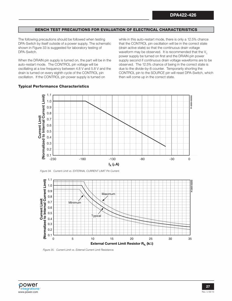
Rev. U 06/15
27
DPA422-426
www.power.com
The following precautions should be followed when testing DPA-Switch by itself outside of a power supply. The schematic shown in Figure 33 is suggested for laboratory testing of DPA-Switch.
When the DRAIN pin supply is turned on, the part will be in the auto-restart mode. The CONTROL pin voltage will be oscillating at a low frequency between 4.8 V and 5.8 V and the drain is turned on every eighth cycle of the CONTROL pin oscillation. If the CONTROL pin power supply is turned on
while in this auto-restart mode, there is only a 12.5% chance that the CONTROL pin oscillation will be in the correct state (drain active state) so that the continuous drain voltage waveform may be observed. It is recommended that the VC power supply be turned on first and the DRAIN pin power supply second if continuous drain voltage waveforms are to be observed. The 12.5% chance of being in the correct state is due to the divide-by-8 counter. Temporarily shorting the CONTROL pin to the SOURCE pin will reset DPA-Switch, which then will come up in the correct state.
BENCH TEST PRECAUTIONS FOR EVALUATION OF ELECTRICAL CHARACTERISTICS
Typical Performance Characteristics
0.1
0.2
0.3
0.4
0.5
0.6
0.7
0.8
0.9
1.1
1.0
-230 -180 -130 -80 -30
IX (µA)
Cur
rent
Lim
it(N
orm
aliz
ed t
o In
tern
al C
urre
nt L
imit
)
0
PI-
2838
-032
202
Figure 34. Current Limit vs. EXTERNAL CURRENT LIMIT Pin Current.
0.3
0.2
0.1
0.5
0.4
0.6
0.7
0.8
0.9
1.0
1.1
0 5 10 15 20 25 30 35
External Current Limit Resistor RIL (kΩ)
Cur
rent
Lim
it(N
orm
aliz
ed t
o In
tern
al C
urre
nt L
imit
)
PI-
2839
-032
202
Minimum
Typical
Maximum
Figure 35. Current Limit vs. External Current Limit Resistance.
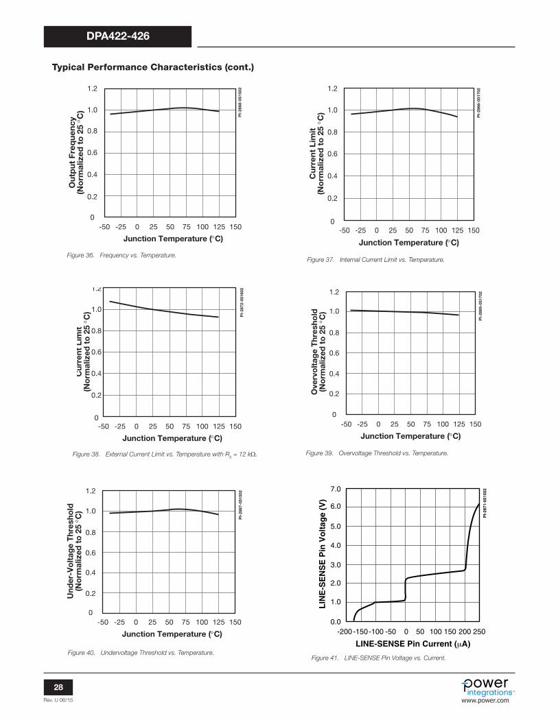
Rev. U 06/15
28
DPA422-426
www.power.com
1.2
1.0
0.8
0.6
0.4
0.2
0-50 -25 0 25 50 75 100 125 150
Junction Temperature (°C)
PI-
2872
-051
602
Cur
rent
Lim
it(N
orm
aliz
ed t
o 25
°C
)
1.2
1.0
0.8
0.6
0.4
0.2
0-50 -25 0 25 50 75 100 125 150
Junction Temperature (°C)
PI-
2865
-051
702
Ove
rvo
ltag
e T
hres
hold
(No
rmal
ized
to
25 °C
)
Figure 38. External Current Limit vs. Temperature with RIL = 12 kW. Figure 39. Overvoltage Threshold vs. Temperature.
1.2
1.0
0.8
0.6
0.4
0.2
0-50 -25 0 25 50 75 100 125 150
Junction Temperature (°C)
PI-
2867
-051
502
Und
er-V
olta
ge T
hres
hold
(Nor
mal
ized
to
25 °
C)
7.0
4.0
6.0
5.0
0.0-200 -100 -50-150 0 50 100 150 200 250
LINE-SENSE Pin Current ( A)
LIN
E-S
EN
SE
Pin
Vo
ltag
e (V
)
PI-
2871
-051
502
2.0
1.0
3.0
Figure 40. Undervoltage Threshold vs. Temperature.Figure 41. LINE-SENSE Pin Voltage vs. Current.
1.2
1.0
0.8
0.6
0.4
0.2
0-50 -25 0 25 50 75 100 125 150
Junction Temperature (°C)P
I-28
68-0
5150
2
Ou
tpu
t F
req
uen
cy(N
orm
aliz
ed t
o 2
5 °C
)
Figure 36. Frequency vs. Temperature.
1.2
1.0
0.8
0.6
0.4
0.2
0-50 -25 0 25 50 75 100 125 150
Junction Temperature (°C)
PI-
2866
-051
702
Cu
rren
t L
imit
(No
rmal
ized
to
25 °C
)
Figure 37. Internal Current Limit vs. Temperature.
Typical Performance Characteristics (cont.)
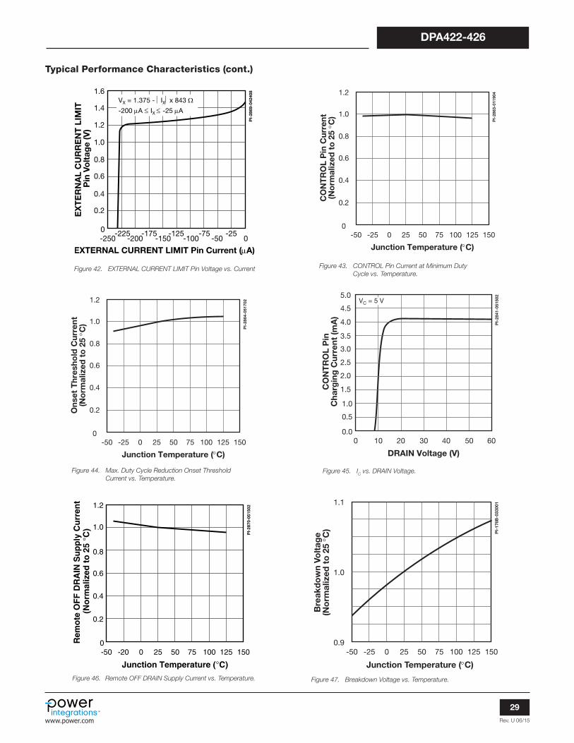
Rev. U 06/15
29
DPA422-426
www.power.com
Typical Performance Characteristics (cont.)
1.2
1.0
0.8
0.6
0.4
0.2
0-50 -25 0 25 50 75 100 125 150
Junction Temperature (°C)
PI-
2863
-011
904
CO
NT
RO
L P
in C
urre
nt(N
orm
aliz
ed t
o 2
5 °C
)
Figure 43. CONTROL Pin Current at Minimum Duty Cycle vs. Temperature.
1.6
1.0
1.4
1.2
0 -225-250 -150
-175-200
-125-50
-25-100
-750
EXTERNAL CURRENT LIMIT Pin Current (µA)
EX
TE
RN
AL
CU
RR
EN
T L
IMIT
P
in V
olt
age
(V)
PI-
2869
-042
408
0.4
0.2
0.6
0.8
VX = 1.375 - IXx 843 Ω-200 µA ≤ IX ≤ -25 µA
Figure 42. EXTERNAL CURRENT LIMIT Pin Voltage vs. Current
5.0
3.5
3.0
4.0
4.5
0.00 10 20 30 40 50 60
DRAIN Voltage (V)
CO
NT
RO
L P
inC
harg
ing
Cur
rent
(mA
)
PI-
2841
-051
502
1.0
0.5
1.5
2.5
2.0
VC = 5 V
Figure 45. IC vs. DRAIN Voltage.
1.2
1.0
0.8
0.6
0.4
0.2
0-50 -25 0 25 50 75 100 125 150
Junction Temperature (°C)
PI-
2864
-051
702
Ons
et T
hres
hold
Cur
rent
(No
rmal
ized
to
25 °C
)
Figure 44. Max. Duty Cycle Reduction Onset Threshold Current vs. Temperature.
1.1
1.0
0.9-50 -25 0 25 50 75 100 125 150
Junction Temperature (°C)
Bre
akd
ow
n Vo
ltag
e(N
orm
aliz
ed t
o 2
5 °C
) PI-
176B
-033
001
Figure 47. Breakdown Voltage vs. Temperature.
1.2
0.8
1.0
0-50 -20 0 25 50 75 100 125 150
Junction Temperature ( C)
Rem
ote
OF
F D
RA
IN S
up
ply
Cu
rren
t (
No
rmal
ized
to
25
C)
PI-
2870
-051
502
0.2
0.4
0.6
Figure 46. Remote OFF DRAIN Supply Current vs. Temperature.

Rev. U 06/15
30
DPA422-426
www.power.com
Typical Performance Characteristics (cont.)
20
16
18
14
12
10
8
6
4
2
00 1 2 3 4 5
Drain Voltage (V)P
I-28
49-0
5030
2
Dra
in C
urre
nt (A
)
Scaling Factors: DPA423 = 0.18 DPA424 = 0.36 DPA425 = 0.72 DPA426 = 1.00
TCASE = 25 °C
TCASE = 100 °C
Figure 48. Output Characteristics.
2.5
2
1.5
1
0.5
0-50 -25 0 25 7550 100 125 150
Temperature (°C)
PI-
2850
-011
904
On-
resi
stan
ce(N
orm
aliz
ed t
o 2
5 °C
)
Figure 49. On-Resistance vs. Temperature.
0 20 40 60 80 100 120 140 16010
100
1000
10000
PI-
2851
-011
904
DRAIN Voltage (V)
Cap
acit
ance
(pF)
Scaling Factors: DPA423 = 0.18 DPA424 = 0.36 DPA425 = 0.72 DPA426 = 1.00
Figure 50. COSS vs. DRAIN Voltage.
2.5
2
1.5
1
0.5
00 0.1 0.2 0.3 0.4 0.5 0.6 0.7 0.8 0.9 1
In-Circuit Peak Drain Current Normalized to Nominal Device Internal Current Limit
PI-
2877
-061
704
Sw
itch
ing
Lo
ss (W
) at
400
kHz
Scaling Factors: DPA423 = 0.08 DPA424 = 0.20 DPA425 = 0.55 DPA426 = 1.00
Data taken from a typicalforward converter design.
Figure 51. Typical Switching Loss.

Rev. U 06/15
31
DPA422-426
www.power.com
PI-2076-040110
1
A
K
J1
4
L
G
8 5
C
N
PDIP-8 (P Package)
D S .004 (.10)
J2
-E-
-D-
B
-F-
DIM
ABCGHJ1J2 KLMNPQ
Inches
0.367-0.3870.240-0.260 0.125-0.1450.015-0.0400.120-0.1400.057-0.0680.014-0.0220.008-0.0150.100 BSC0.030 (MIN)0.300-0.3200.300-0.3900.300 BSC
mm
9.32-9.836.10-6.603.18-3.680.38-1.023.05-3.561.45-1.730.36-0.560.20-0.382.54 BSC0.76 (MIN)7.62-8.137.62-9.917.62 BSC
Notes:1. Package dimensions conform to JEDEC specification MS-001-AB for standard dual in-line (DIP) package .300 inch row spacing (PLASTIC) 8 leads (issue B, 7/85).2. Controlling dimensions are inches.3. Dimensions shown do not include mold flash or other protrusions. Mold flash or protrusions shall not exceed .006 (.15) on any side. 4. D, E and F are reference datums on the molded body.
H
M
P
Q P08A
PI-2077-040110
1
A
J1
4L
8 5
C
G08A
SMD-8 (G Package)D S .004 (.10)
J2
E S .010 (.25)
-E-
-D-
B
-F-
M
J3
DIM
ABCGHJ1J2J3J4 KLMPα
Inches
0.367-0.3870.240-0.260 0.125-0.1450.004-0.0120.036-0.0440.057-0.0680.048-0.0530.032-0.0370.007-0.0110.010-0.0120.100 BSC0.030 (MIN)0.372-0.388
0-8°
mm
9.32-9.836.10-6.603.18-3.680.10-0.300.91-1.121.45-1.731.22-1.350.81-0.940.18-0.280.25-0.302.54 BSC0.76 (MIN)9.45-9.86
0-8°
Notes:1. Package dimensions conform to JEDEC specification MS-001-AB (issue B, 7/85) except for lead shape and size.2. Controlling dimensions are inches. 3. Dimensions shown do not include mold flash or other protrusions. Mold flash or protrusions shall not exceed .006 (.15) on any side.4. D, E and F are reference datums on the molded body.
K
Gα
H
.004 (.10)J4
P
.010 (.25) M A S
.420
.046 .060 .060 .046
.080Pin 1
.086.186
.286
Solder Pad Dimensions
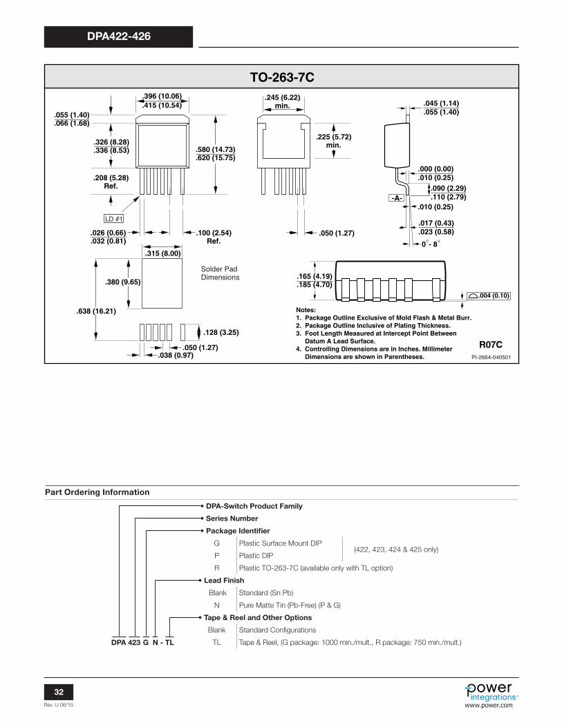
Rev. U 06/15
32
DPA422-426
www.power.com
.165 (4.19)
.185 (4.70)
R07C
TO-263-7C
-A-
.580 (14.73)
.620 (15.75)
.396 (10.06)
.415 (10.54)
.326 (8.28)
.336 (8.53)
.055 (1.40)
.066 (1.68)
.100 (2.54)Ref.
.208 (5.28)Ref.
.026 (0.66)
.032 (0.81)
.225 (5.72)min.
.245 (6.22)min.
.000 (0.00)
.010 (0.25)
.010 (0.25)
.090 (2.29)
.110 (2.79)
.017 (0.43)
.023 (0.58) °8 -°0
.045 (1.14)
.055 (1.40)
.050 (1.27)
Notes:1. Package Outline Exclusive of Mold Flash & Metal Burr.2. Package Outline Inclusive of Plating Thickness.3. Foot Length Measured at Intercept Point Between Datum A Lead Surface.4. Controlling Dimensions are in Inches. Millimeter Dimensions are shown in Parentheses.
.004 (0.10)
.315 (8.00)
.128 (3.25)
.038 (0.97) .050 (1.27)
.380 (9.65)
.638 (16.21)
Part Ordering Information
• DPA-Switch Product Family
• Series Number
• Package Identifier
G Plastic Surface Mount DIP (422, 423, 424 & 425 only)
P Plastic DIP
R Plastic TO-263-7C (available only with TL option)
• Lead Finish
Blank Standard (Sn Pb)
N Pure Matte Tin (Pb-Free) (P & G)
• Tape & Reel and Other Options
Blank Standard Configurations
TL Tape & Reel, (G package: 1000 min./mult., R package: 750 min./mult.)DPA 423 G N - TL

Rev. U 06/15
33
DPA422-426
www.power.com
Revision Notes Date
F Final release data sheet. 6/02
G Updated Figure 25 and text description. 9/02
H
Corrected missing text on page 9 and corrected Table 4. Updated R package description. Revised thermal impedances (qJA), DCMIN, VF, IF, and BVDSS. Updated Figure 25 and description in text.
4/03
I Corrected text errors on pp. 1, 7 and 20. 5/03
J Figure 25 and description in text updated. 5/03
K Added P and G packages. 1/04
L Corrected Figure 3. 4/04
MAdded package information to Table 1. Revised Figure 13. Added lead-free ordering information.
12/04
N Minor error corrections. 2/05
O Added S-PAK. 7/05
P Added notes to Table 6. 7/05
Q Updated Figure 27 to best reflect current requirements for PoE. 5/06
R Added DPA422. 2/07
S Removed S-Pack. 12/07
T Added Note 8, page 1. 12/12
U Updated with new Brand Logo. 06/15

For the latest updates, visit our website: www.power.comPower Integrations reserves the right to make changes to its products at any time to improve reliability or manufacturability. Power Integrations does not assume any liability arising from the use of any device or circuit described herein. POWER INTEGRATIONS MAKES NO WARRANTY HEREIN AND SPECIFICALLY DISCLAIMS ALL WARRANTIES INCLUDING, WITHOUT LIMITATION, THE IMPLIED WARRANTIES OF MERCHANTABILITY, FITNESS FOR A PARTICULAR PURPOSE, AND NON-INFRINGEMENT OF THIRD PARTY RIGHTS.
Patent InformationThe products and applications illustrated herein (including transformer construction and circuits external to the products) may be covered by one or more U.S. and foreign patents, or potentially by pending U.S. and foreign patent applications assigned to Power Integrations. A complete list of Power Integrations patents may be found at www.power.com. Power Integrations grants its customers a license under certain patent rights as set forth at http://www.power.com/ip.htm.
Life Support PolicyPOWER INTEGRATIONS PRODUCTS ARE NOT AUTHORIZED FOR USE AS CRITICAL COMPONENTS IN LIFE SUPPORT DEVICES OR SYSTEMS WITHOUT THE EXPRESS WRITTEN APPROVAL OF THE PRESIDENT OF POWER INTEGRATIONS. As used herein:
1. A Life support device or system is one which, (i) is intended for surgical implant into the body, or (ii) supports or sustains life, and (iii) whose failure to perform, when properly used in accordance with instructions for use, can be reasonably expected to result in significant injury or death to the user.
2. A critical component is any component of a life support device or system whose failure to perform can be reasonably expected to cause the failure of the life support device or system, or to affect its safety or effectiveness.
The PI logo, TOPSwitch, TinySwitch, LinkSwitch, LYTSwitch, InnoSwitch, DPA-Switch, PeakSwitch, CAPZero, SENZero, LinkZero, HiperPFS, HiperTFS, HiperLCS, Qspeed, EcoSmart, Clampless, E-Shield, Filterfuse, FluxLink, StakFET, PI Expert and PI FACTS are trademarks of Power Integrations, Inc. Other trademarks are property of their respective companies. ©2015, Power Integrations, Inc.
Power Integrations Worldwide Sales Support Locations
World Headquarters5245 Hellyer AvenueSan Jose, CA 95138, USA.Main: +1-408-414-9200Customer Service:Phone: +1-408-414-9665Fax: +1-408-414-9765e-mail: [email protected]
China (Shanghai)Rm 1601/1610, Tower 1,Kerry Everbright CityNo. 218 Tianmu Road West,Shanghai, P.R.C. 200070Phone: +86-21-6354-6323Fax: +86-21-6354-6325e-mail: [email protected]
China (Shenzhen)17/F, Hivac Building, No. 2,Keji Nan 8th Road, Nanshan District, Shenzhen, China, 518057Phone: +86-755-8672-8689Fax: +86-755-8672-8690e-mail: [email protected]
GermanyLindwurmstrasse 11480337 MunichGermanyPhone: +49-895-527-39110Fax: +49-895-527-39200e-mail: [email protected]
India#1, 14th Main RoadVasanthanagarBangalore-560052 IndiaPhone: +91-80-4113-8020Fax: +91-80-4113-8023e-mail: [email protected]
ItalyVia Milanese 20, 3rd. Fl.20099 Sesto San Giovanni (MI)ItalyPhone: +39-024-550-8701Fax: +39-028-928-6009e-mail: [email protected]
JapanKosei Dai-3 Bldg. 2-12-11, Shin-Yokohama, Kohoku-ku Yokohama-shi Kanagwan 222-0033 JapanPhone: +81-45-471-1021Fax: +81-45-471-3717e-mail: [email protected]
KoreaRM 602, 6FLKorea City Air Terminal B/D, 159-6Samsung-Dong, Kangnam-Gu,Seoul, 135-728, KoreaPhone: +82-2-2016-6610Fax: +82-2-2016-6630e-mail: [email protected]
Singapore51 Newton Road#19-01/05 Goldhill PlazaSingapore, 308900Phone: +65-6358-2160Fax: +65-6358-2015e-mail: [email protected]
Taiwan5F, No. 318, Nei Hu Rd., Sec. 1Nei Hu Dist.Taipei 11493, Taiwan R.O.C.Phone: +886-2-2659-4570Fax: +886-2-2659-4550e-mail: [email protected]
UKFirst Floor, Unit 15, MeadwayCourt, Rutherford Close,Stevenage, Herts. SG1 2EFUnited KingdomPhone: +44 (0) 1252-730-141Fax: +44 (0) 1252-727-689e-mail: [email protected]