Embed Size (px)
Citation preview
Double-layer Fano resonance photonic crystal filters
Yichen Shuai,1 Deyin Zhao,1 Zhaobing Tian,2 Jung-Hun Seo,3 David V. Plant,2 Zhenqiang Ma,3 Shanhui Fan,4 and Weidong Zhou1,*
1Department of Electrical Engineering, NanoFAB Center, University of Texas at Arlington, Texas 76019, USA 2Department of Electrical and Computer Engineering, McGill University, Montreal, QC H3A 2A7, Canada
3Department of Electrical and Computer Engineering, University of Wisconsin-Madison, Wisconsin 53706, USA 4Department of Electrical Engineering, Ginzton Laboratory, Stanford University, Stanford, California 94305, USA
Abstract: We report ultra-compact surface-normal high-Q optical filters based on single- and double-layer stacked Fano resonance photonic crystal slabs on both Si and quartz substrates. A single layer photonic crystal filter was designed and a Q factor of 1,737 was obtained with 23 dB extinction ratio. With stacked double-layer photonic crystal configuration, the optical filter Q can increase to over 10,000,000 in design. Double-layer filters with quality factor of 9,734 and extinction ratio of 8 dB were experimentally demonstrated, for a filter design with target Q of 22,000. ©2013 Optical Society of America OCIS codes: (050.5298) Photonic crystals; (350.2460) Optical filters; (350.4238) Nanophotonics and photonic crystals.
References and links
1. A. E. Miroshnichenko, S. Flach, and Y. S. Kivshar, “Fano resonances in nanoscale structures,” Rev. Mod. Phys. 82(3), 2257–2298 (2010).
2. B. Luk’yanchuk, N. I. Zheludev, S. A. Maier, N. J. Halas, P. Nordlander, H. Giessen, and C. T. Chong, “The Fano resonance in plasmonic nanostructures and metamaterials,” Nat. Mater. 9(9), 707–715 (2010).
3. S. Fan and J. D. Joannopoulos, “Analysis of guided resonances in photonic crystal slabs,” Phys. Rev. B 65(23), 235112 (2002).
4. V. Liu, M. Povinelli, and S. Fan, “Resonance-enhanced optical forces between coupled photonic crystal slabs,” Opt. Express 17(24), 21897–21909 (2009).
5. W. Zhou, Z. Ma, H. Yang, Z. Qiang, G. Qin, H. Pang, L. Chen, W. Yang, S. Chuwongin, and D. Zhao, “Flexible photonic-crystal Fano filters based on transferred semiconductor nanomembranes,” J. Phys. D. 42(23), 234007 (2009).
6. W. Suh, M. F. Yanik, O. Solgaard, and S. Fan, “Displacement-sensitive photonic crystal structures based on guided resonance in photonic crystal slabs,” Appl. Phys. Lett. 82(13), 1999 (2003).
7. R. Magnusson and S. S. Wang, “New principle for optical filters,” Appl. Phys. Lett. 61(9), 1022 (1992). 8. R. Magnusson and M. Shokooh-Saremi, “Physical basis for wideband resonant reflectors,” Opt. Express 16(5),
3456–3462 (2008). 9. M. C. Huang, Y. Zhou, and C. J. Chang-Hasnain, “A surface-emitting laser incorporating a high-index-contrast
subwavelength grating,” Nat. Photonics 1(2), 119–122 (2007). 10. C. J. Chang-Hasnain, “High-contrast gratings as a new platform for integrated optoelectronics,” Semicond. Sci.
Technol. 26(1), 014043 (2011). 11. Y. Kanamori, T. Kitani, and K. Hane, “Control of guided resonance in a photonic crystal slab using
microelectromechanical actuators,” Appl. Phys. Lett. 90(3), 031911 (2007). 12. K. B. Crozier, V. Lousse, O. Kilic, S. Kim, S. Fan, and O. Solgaard, “Air-bridged photonic crystal slabs at
visible and near-infrared wavelengths,” Phys. Rev. B 73(11), 115126 (2006). 13. C. Grillet, D. Freeman, B. Luther-Davies, S. Madden, R. McPhedran, D. J. Moss, M. J. Steel, and B. J. Eggleton,
“Characterization and modeling of Fano resonances in chalcogenide photonic crystal membranes,” Opt. Express 14(1), 369–376 (2006).
14. L. Zhou and A. W. Poon, “Fano resonance-based electrically reconfigurable add-drop filters in silicon microring resonator-coupled Mach-Zehnder interferometers,” Opt. Lett. 32(7), 781–783 (2007).
15. S. Fan, “Sharp asymmetric line shapes in side-coupled waveguide-cavity systems,” Appl. Phys. Lett. 80(6), 908 (2002).
16. L. Y. Mario, S. Darmawan, and M. K. Chin, “Asymmetric Fano resonance and bistability for high extinction ratio, large modulation depth, and low power switching,” Opt. Express 14(26), 12770–12781 (2006).
#195784 - $15.00 USD Received 14 Aug 2013; revised 27 Sep 2013; accepted 27 Sep 2013; published 7 Oct 2013(C) 2013 OSA 21 October 2013 | Vol. 21, No. 21 | DOI:10.1364/OE.21.024582 | OPTICS EXPRESS 24582
17. C. Y. Chao and L. J. Guo, “Biochemical sensors based on polymer microrings with sharp asymmetrical resonance,” Appl. Phys. Lett. 83(8), 1527 (2003).
18. W. Suh, O. Solgaard, and S. Fan, “Displacement sensing using evanescent tunneling between guided resonances in photonic crystal slabs,” J. Appl. Phys. 98(3), 033102 (2005).
19. A. Rosenberg, M. Carter, J. Casey, M. Kim, R. Holm, R. Henry, C. Eddy, V. Shamamian, K. Bussmann, S. Shi, and D. W. Prather, “Guided resonances in asymmetrical GaN photonic crystal slabs observed in the visible spectrum,” Opt. Express 13(17), 6564–6571 (2005).
20. N. Inoue and T. Baba, “External control of guided resonance in photonic crystal slab by changing the index anisotropy of liquid crystal,” Proc. SPIE 6352, 63520R, 63520R-8 (2006).
21. O. Levi, M. M. Lee, J. Zhang, V. Lousse, S. R. J. Brueck, S. Fan, and J. S. Harris, “Sensitivity analysis of a photonic crystal structure for index-of-refraction sensing,” Proc. SPIE 6447, 64470P, 64470P-9 (2007).
22. R. Harbers, S. Jochim, N. Moll, R. F. Mahrt, D. Erni, J. A. Hoffnagle, and W. D. Hinsberg, “Control of Fano line shapes by means of photonic crystal structures in a dye-doped polymer,” Appl. Phys. Lett. 90(20), 201105 (2007).
23. E. Bisaillon, D. Tan, B. Faraji, A. Kirk, L. Chrowstowski, and D. V. Plant, “High reflectivity air-bridge subwavelength grating reflector and Fabry-Perot cavity in AlGaAs/GaAs,” Opt. Express 14(7), 2573–2582 (2006).
24. J. H. Kim, L. Chrostowski, E. Bisaillon, and D. V. Plant, “DBR, Sub-wavelength grating, and Photonic crystal slab Fabry-Perot cavity design using phase analysis by FDTD,” Opt. Express 15(16), 10330–10339 (2007).
25. S. Boutami, B. Benbakir, X. Letartre, J. L. Leclercq, P. Regreny, and P. Viktorovitch, “Ultimate vertical Fabry-Perot cavity based on single-layer photonic crystal mirrors,” Opt. Express 15(19), 12443–12449 (2007).
26. C. Sciancalepore, B. B. Bakir, X. Letartre, J. Harduin, N. Olivier, C. Seassal, J. Fedeli, and P. Viktorovitch, “CMOS-compatible ultra-compact 1.55- um emitting VCSELs using double photonic crystal mirrors,” IEEE Photon. Technol. Lett. 24(6), 455–457 (2012).
27. H. Yang, D. Zhao, S. Chuwongin, J. H. Seo, W. Yang, Y. Shuai, J. Berggren, M. Hammar, Z. Ma, and W. Zhou, “Transfer-printed stacked nanomembrane lasers on silicon,” Nat. Photonics 6(9), 617–622 (2012).
28. H. Yang, Z. Qiang, H. Pang, Z. Ma, and W. D. Zhou, “Surface-Normal Fano Filters Based on Transferred Silicon Nanomembranes on Glass Substrates,” Electron. Lett. 44(14), 858–859 (2008).
29. Z. Qiang, H. Yang, L. Chen, H. Pang, Z. Ma, and W. Zhou, “Fano filters based on transferred silicon nanomembranes on plastic substrates,” Appl. Phys. Lett. 93(6), 061106 (2008).
30. L. Chen, Z. Qiang, H. Yang, H. Pang, Z. Ma, and W. D. Zhou, “Polarization and angular dependent transmissions on transferred nanomembrane Fano filters,” Opt. Express 17(10), 8396–8406 (2009).
31. M. Meitl, Z. Zhu, V. Kumar, K. Lee, X. Feng, Y. Huang, I. Adesida, R. Nuzzo, and J. Rogers, “Transfer printing by kinetic control of adhesion to an elastomeric stamp,” Nat. Mater. 5(1), 33–38 (2005).
32. H. Yang, D. Zhao, J. Seo, S. Kim, J. Rogers, Z. Ma, and W. Zhou, “Broadband Membrane Reflectors on Glass,” IEEE Photon. Technol. Lett. 24(6), 476–478 (2012).
33. M. Lipson, “Guiding, modulating, and emitting light on silicon-challenges and opportunities,” J. Lightwave Technol. 23(12), 4222–4238 (2005).
34. D. Kwong, J. Covey, A. Hosseini, Y. Zhang, X. Xu, and R. T. Chen, “Ultralow-loss polycrystalline silicon waveguides and high uniformity 1x12 MMI fanout for 3D photonic integration,” Opt. Express 20(19), 21722–21728 (2012).
35. V. Liu and S. Fan, “S4: A free electromagnetic solver for layered periodic structures,” Comput. Phys. Commun. 183(10), 2233–2244 (2012).
36. Y. Shuai, D. Zhao, Z. Tian, J. H. Seo, R. Jacobson, D. V. Plant, M. G. Lagally, S. Fan, Z. Ma, and W. Zhou, “Stacked Fano Resonance Photonic Crystal Nanomembrane High-Q Filters,” in IEEE Photonics Conference, San Francisco, CA, 2012.
1. Introduction
Recently, Fano resonances, known from atomic physics, have been employed for a wide variety of nanophotonic structures, such as quantum dots, photonic crystals (PhCs), plasmonics, and metamaterials [1–4]. With modal dispersion engineering, Fano filters and reflectors can all be realized in single-layer dielectric PhC structures [3, 5, 6]. With in-plane periodic modulation of dielectric constant in PhC slabs (PCS), the out-of-the-plane optical mode coupling is feasible with the Fano resonance effect, where the in-plane guided resonances above the lightline are strongly coupled to the out-of-the-plane radiation modes due to the phase matching provided by the periodic lattice structure. Therefore, these guided resonances can provide an efficient way to channel light from within the slab to the external environment, and vice versa. Such phenomenon was also investigated in one-dimensional grating structures, known as guided mode resonances (GMRs) [7, 8], or high index contrast gratings (HCGs) [9, 10]. The investigation of guided resonance has resulted in using various one dimensional (1D) and two dimensional (2D) dielectric structures in applications, such as
#195784 - $15.00 USD Received 14 Aug 2013; revised 27 Sep 2013; accepted 27 Sep 2013; published 7 Oct 2013(C) 2013 OSA 21 October 2013 | Vol. 21, No. 21 | DOI:10.1364/OE.21.024582 | OPTICS EXPRESS 24583
filters [6, 11–14], modulators [15, 16], sensors [17, 18], as well as broadband reflectors, lasers, and beam shaping structures, etc [11, 19–27].
In previous works, we reported Fano resonance filters on both glass and plastic substrate, employing polydimethylsiloxane (PDMS) transfer printing technique [5, 28–30]. However, single layer PhC Fano filters offer limited quality factor Q and limited dispersion engineering capabilities for fine-tuning the output spectrum. It was reported that much higher Q Fano filters can be realized by multi-layer PhC coupling and lattice offset control [4, 6]. Employing PDMS transfer printing technique [31, 32] and poly-crystalline-Si deposition processes [33, 34], we report here single- and double-layer Fano filters on silicon and on quartz substrates, with symmetric spectral lineshapes and much higher Q factors of 98,000-10,000,000 by design. We experimentally demonstrated double-layer filters with Q factors of 22,000 by design and ~10,000 by measurement. These high Q filters, can have extraordinary potentials in integrated photonics, optical communications, and sensing applications.
2. Device design
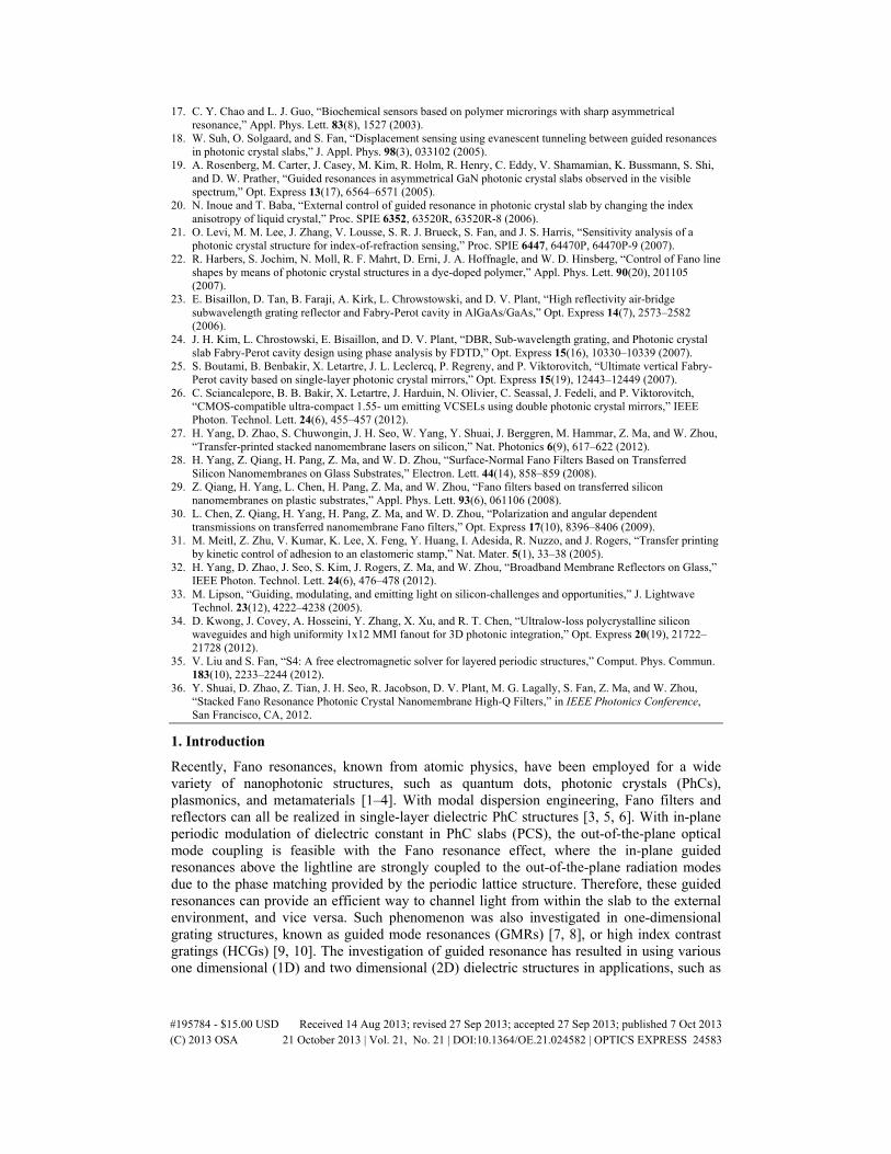
Shown in Fig. 1 are the schematics of double-layer Fano resonance PhC optical filters on low index glass substrates, where key lattice parameters are defined as air hole radius (r), lattice period (a), thicknesses for top (t1), bottom (t2) Si PhC layers and the oxide buffer layer (tb) in between. Both single- and double-layer Fano resonance Si PhC filters were designed and optimized for high Q around 1,550 nm spectral band. The transmission spectrum and field plots were computed based on the Fourier Modal Method using a freely available Stanford Stratified Structure Solver (S4) software package [35]. Comparing the commercial RCWA package GD-Calc we used before [36], S4 software package offers much higher resolution due to the consideration of higher diffraction orders and also takes much less computation time. Shown in Table 1 are key design parameters for a few optimized design structures, where S1-S3 are for single-layer and D1-D3 are for double-layer designs.
(a) (b)
t1
t2tb
ar
Fig. 1. Schematics of double-layer Fano resonance photonic crystal optical filters: (a) A 3D sketch; and (b) Key parameters defined for the square lattice photonic crystal double layer.
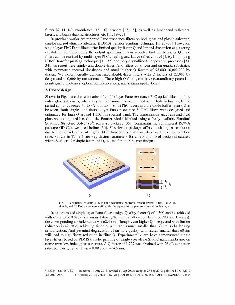
In an optimized single layer Fano filter design, Quality factor Q of 4,500 can be achieved with r/a ratio of 0.08, as shown in Table 1, S3. For the lattice constant a of 780 nm (Case S3), the corresponding air hole radius r is 62.4 nm. Though even higher Q is expected with further reduction in r/a ratio, achieving air holes with radius much smaller than 60 nm is challenging in fabrication. And potential degradation of air hole quality with radius smaller than 60 nm will lead to significant reduction in filter Q. Experimentally, we have demonstrated single layer filters based on PDMS transfer printing of single crystalline Si PhC nanomembranes on transparent low index glass substrate. A Q factor of 1,727 was obtained with 26 dB extinction ratio, for Design S1 with r/a = 0.08 and a = 765 nm.
#195784 - $15.00 USD Received 14 Aug 2013; revised 27 Sep 2013; accepted 27 Sep 2013; published 7 Oct 2013(C) 2013 OSA 21 October 2013 | Vol. 21, No. 21 | DOI:10.1364/OE.21.024582 | OPTICS EXPRESS 24584
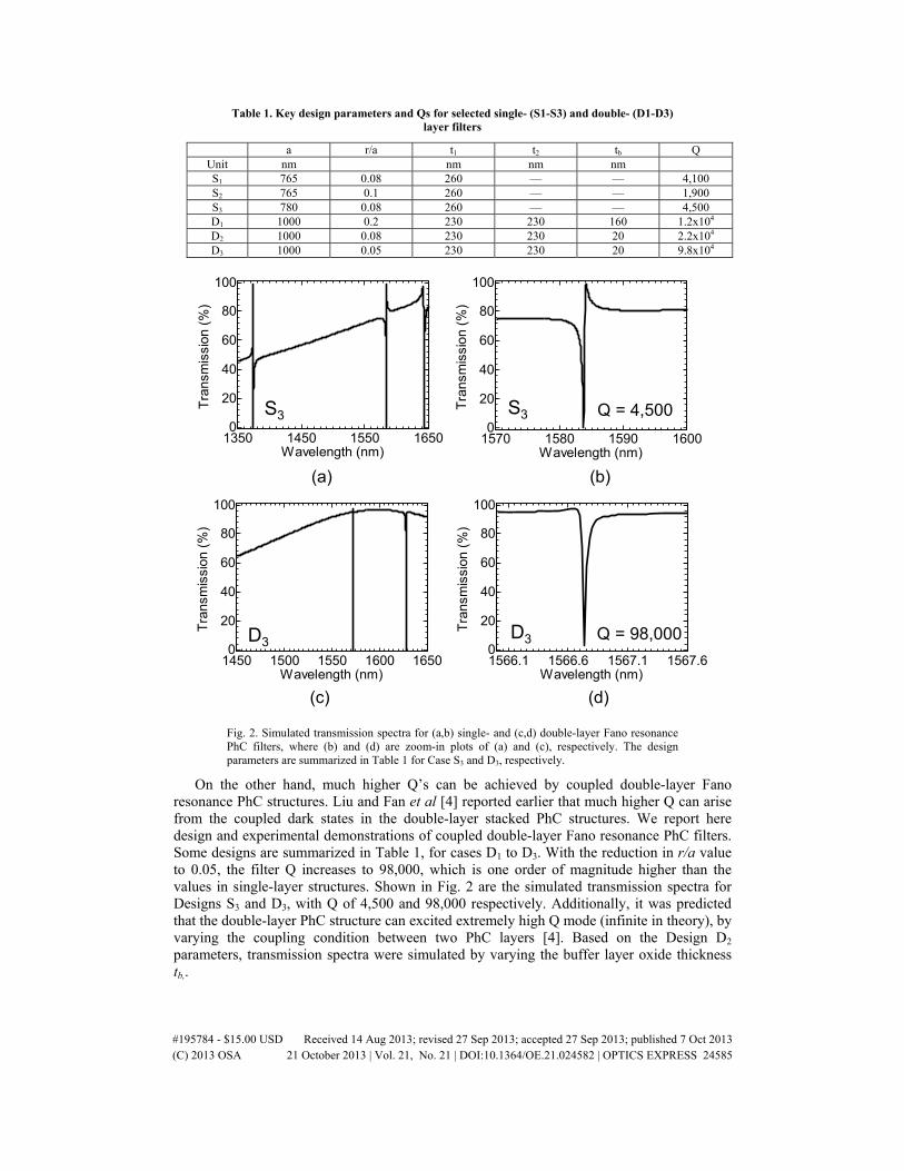
Table 1. Key design parameters and Qs for selected single- (S1-S3) and double- (D1-D3) layer filters
a r/a t1 t2 tb Q Unit nm nm nm nm S1 765 0.08 260 — — 4,100 S2 765 0.1 260 — — 1,900 S3 780 0.08 260 — — 4,500 D1 1000 0.2 230 230 160 1.2x10⁴ D2 1000 0.08 230 230 20 2.2x10⁴ D3 1000 0.05 230 230 20 9.8x10⁴
Q = 98,000
1570 1580 1590 16000
20
40
60
80
100
Wavelength (nm)T
rans
mis
sion
(%
)
1566.1 1566.6 1567.1 1567.60
20
40
60
80
100
Wavelength (nm)
Tra
nsm
issi
on (
%)
(a) (b)
(c) (d)
Q = 4,500
1350 1450 1550 16500
20
40
60
80
100
Wavelength (nm)
Tra
nsm
issi
on (
%)
1450 1500 1550 1600 16500
20
40
60
80
100
Wavelength (nm)
Tra
nsm
issi
on (
%)
Q = 98,000D3D3
S3S3
Fig. 2. Simulated transmission spectra for (a,b) single- and (c,d) double-layer Fano resonance PhC filters, where (b) and (d) are zoom-in plots of (a) and (c), respectively. The design parameters are summarized in Table 1 for Case S3 and D3, respectively.
On the other hand, much higher Q’s can be achieved by coupled double-layer Fano resonance PhC structures. Liu and Fan et al [4] reported earlier that much higher Q can arise from the coupled dark states in the double-layer stacked PhC structures. We report here design and experimental demonstrations of coupled double-layer Fano resonance PhC filters. Some designs are summarized in Table 1, for cases D1 to D3. With the reduction in r/a value to 0.05, the filter Q increases to 98,000, which is one order of magnitude higher than the values in single-layer structures. Shown in Fig. 2 are the simulated transmission spectra for Designs S3 and D3, with Q of 4,500 and 98,000 respectively. Additionally, it was predicted that the double-layer PhC structure can excited extremely high Q mode (infinite in theory), by varying the coupling condition between two PhC layers [4]. Based on the Design D2 parameters, transmission spectra were simulated by varying the buffer layer oxide thickness tb,.
#195784 - $15.00 USD Received 14 Aug 2013; revised 27 Sep 2013; accepted 27 Sep 2013; published 7 Oct 2013(C) 2013 OSA 21 October 2013 | Vol. 21, No. 21 | DOI:10.1364/OE.21.024582 | OPTICS EXPRESS 24585
For the double-layer structure, the simulated transmission spectra are plotted in Fig. 3(a), with oxide buffer thicknesses range from 0 to 160 nm. With the increase of oxide buffer layer thicknesses, the high Q modes (shorter wavelength modes shown in Fig. 3(a) shift towards shorter wavelengths, with the filter Q value maximizes around 10,000,000 for buffer layer thickness tb = 60 nm, as shown in Fig. 3(b). Shown in Fig. 3(c) is the zoom-in spectral plot for the transmission dip with Q of 10,000,000. Simulated field distribution profiles for three cases close to the maximum Q are shown in Fig. 3(d), where strong field confinement is evident for the high Q transmission dips at optimal buffer layer thickness.
1450 1500 1550 1600 16500
2
4
6
8
Wavelength (nm)
Tra
nsm
issi
on
tb=0 nm
20 nm40 nm
60 nm
80 nm
100 nm120 nm
Q~5K
Q~22K
Q~21K
Q~37K
Q~125K
Q~110KQ~1e7
140 nmQ~15K
160 nmQ~12K
0 40 80 120 1601450
1480
1510
1540
1570
1600
Buffer thickness (nm)
Res
onan
t λ (
nm)
103
104
105
106
107
Q fa
ctor
λQ
tb =20 nm λ=1559 nm
tb =60 nm λ=1515 nm
tb =100 nm λ=1489 nm1515.277 1515.279
0
0.2
0.4
0.6
0.8
1
Wavelength (nm)
Tra
nsm
issi
on
(c) (d)
(a) (b)
tb=60 nm Q= 107
Fig. 3. Simulation results for Design D2 with different buffer layer thicknesses tb: (a) Transmission spectra with different tb from 0 nm to 160 nm; (b) High Q resonant wavelengths and the corresponding Q values for different buffer thicknesses tb; (c) Zoom-in spectrum for the buffer thickness tb = 60 nm and filter Q of 10,000,000; and (d) Simulated E-field intensity profile at resonant wavelengths for three different tb values, where tb = 60 nm representing the highest Q condition for this design.
3. Device fabrication and characterization
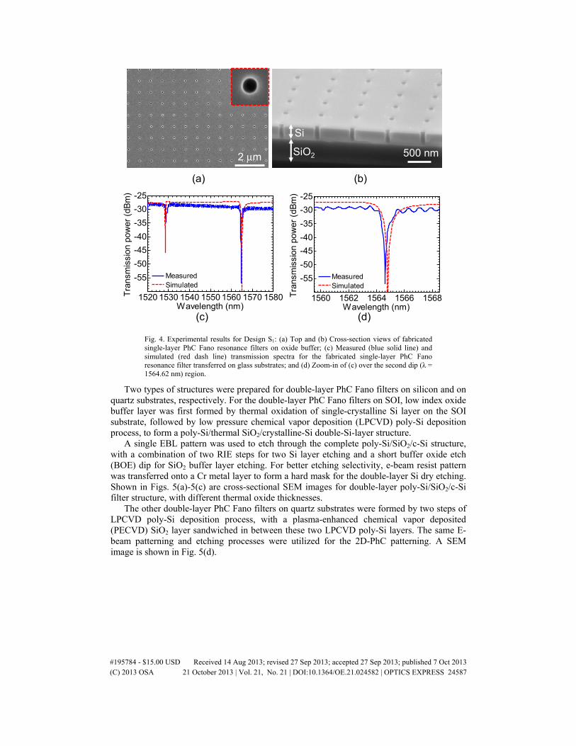
Single-layer Fano resonance PhC filters were first patterned on silicon-on-insulator (SOI) substrates, based on electron-beam lithography (EBL) and reactive-ion etching (RIE) processes. It was then transferred onto glass substrates using transfer printing process [32]. Shown in Figs. 4(a) and 4(b) are scanning electron microscope (SEM) images of the fabricated single layer Fano filters on glass substrate. The single layer Fano filters were characterized with a tunable laser (1 pm tuning step) based setup for transmission measurement over wavelengths of 1490 nm to 1650 nm. The measured (blue solid line) and simulated (red dash line) transmission spectra are shown in Fig. 4(c), with zoom-ins shown in Fig. 4(d). Two transmission dips were found, at 1529.88 nm and 1564.62 nm. For the 1564.62 nm dip, the Q value of 1,737 was obtained, with 26 dB extinction ratio.
#195784 - $15.00 USD Received 14 Aug 2013; revised 27 Sep 2013; accepted 27 Sep 2013; published 7 Oct 2013(C) 2013 OSA 21 October 2013 | Vol. 21, No. 21 | DOI:10.1364/OE.21.024582 | OPTICS EXPRESS 24586
2 μm
Si
SiO2 500 nm
(a) (b)
1520 1530 1540 1550 1560 1570 1580
-55
-50
-45
-40
-35
-30
-25
Wavelength (nm)
Tra
nsm
issi
on p
ower
(dB
m)
MeasuredSimulated
1560 1562 1564 1566 1568
-55
-50
-45
-40
-35
-30
-25
Wavelength (nm)
Tra
nsm
issi
on p
ower
(dB
m)
MeasuredSimulated
(c) (d)
Fig. 4. Experimental results for Design S1: (a) Top and (b) Cross-section views of fabricated single-layer PhC Fano resonance filters on oxide buffer; (c) Measured (blue solid line) and simulated (red dash line) transmission spectra for the fabricated single-layer PhC Fano resonance filter transferred on glass substrates; and (d) Zoom-in of (c) over the second dip (λ = 1564.62 nm) region.
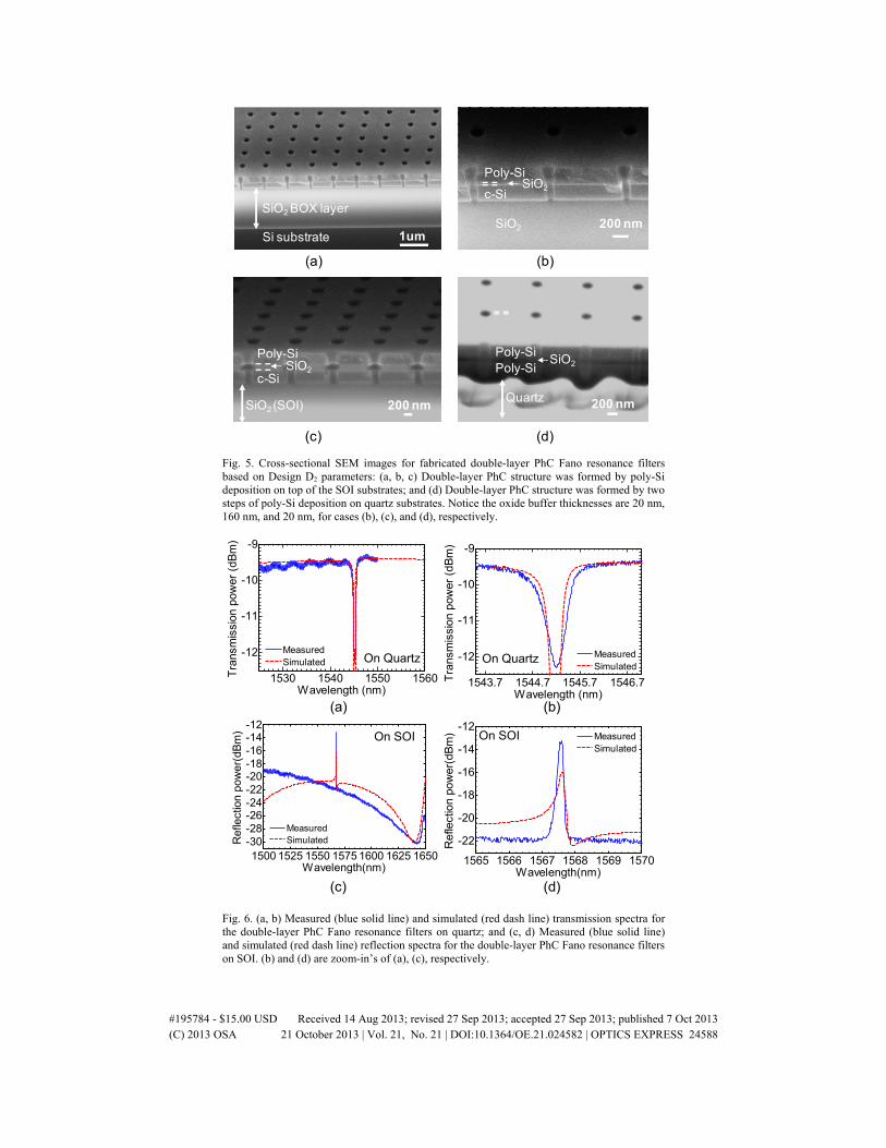
Two types of structures were prepared for double-layer PhC Fano filters on silicon and on quartz substrates, respectively. For the double-layer PhC Fano filters on SOI, low index oxide buffer layer was first formed by thermal oxidation of single-crystalline Si layer on the SOI substrate, followed by low pressure chemical vapor deposition (LPCVD) poly-Si deposition process, to form a poly-Si/thermal SiO2/crystalline-Si double-Si-layer structure.
A single EBL pattern was used to etch through the complete poly-Si/SiO2/c-Si structure, with a combination of two RIE steps for two Si layer etching and a short buffer oxide etch (BOE) dip for SiO2 buffer layer etching. For better etching selectivity, e-beam resist pattern was transferred onto a Cr metal layer to form a hard mask for the double-layer Si dry etching. Shown in Figs. 5(a)-5(c) are cross-sectional SEM images for double-layer poly-Si/SiO2/c-Si filter structure, with different thermal oxide thicknesses.
The other double-layer PhC Fano filters on quartz substrates were formed by two steps of LPCVD poly-Si deposition process, with a plasma-enhanced chemical vapor deposited (PECVD) SiO2 layer sandwiched in between these two LPCVD poly-Si layers. The same E-beam patterning and etching processes were utilized for the 2D-PhC patterning. A SEM image is shown in Fig. 5(d).
#195784 - $15.00 USD Received 14 Aug 2013; revised 27 Sep 2013; accepted 27 Sep 2013; published 7 Oct 2013(C) 2013 OSA 21 October 2013 | Vol. 21, No. 21 | DOI:10.1364/OE.21.024582 | OPTICS EXPRESS 24587
200 nm
Poly-Si
Quartz
Poly-SiSiO2
SiO2 BOX layer
Si substrate 1um
c-Si
SiO2
Poly-SiSiO2
200 nm
c-Si
Poly-Si
200 nm
SiO2
SiO2 (SOI)
(a) (b)
(c) (d)
Fig. 5. Cross-sectional SEM images for fabricated double-layer PhC Fano resonance filters based on Design D2 parameters: (a, b, c) Double-layer PhC structure was formed by poly-Si deposition on top of the SOI substrates; and (d) Double-layer PhC structure was formed by two steps of poly-Si deposition on quartz substrates. Notice the oxide buffer thicknesses are 20 nm, 160 nm, and 20 nm, for cases (b), (c), and (d), respectively.
1543.7 1544.7 1545.7 1546.7
-12
-11
-10
-9
Wavelength (nm)
Tra
nsm
issi
on p
ower
(dB
m)
MeasuredSimulated
1565 1566 1567 1568 1569 1570
-22
-20
-18
-16
-14
-12
Wavelength(nm)
Ref
lect
ion
pow
er(d
Bm
)
MeasuredSimulated
1530 1540 1550 1560
-12
-11
-10
-9
Wavelength (nm)
Tra
nsm
issi
on p
ower
(dB
m)
MeasuredSimulated
1500 1525 1550 1575 1600 1625 1650-30-28-26-24-22-20-18-16-14-12
Wavelength(nm)
Ref
lect
ion
pow
er(d
Bm
)
MeasuredSimulated
On Quartz On Quartz
(a) (b)
On SOI On SOI
(c) (d)
Fig. 6. (a, b) Measured (blue solid line) and simulated (red dash line) transmission spectra for the double-layer PhC Fano resonance filters on quartz; and (c, d) Measured (blue solid line) and simulated (red dash line) reflection spectra for the double-layer PhC Fano resonance filters on SOI. (b) and (d) are zoom-in’s of (a), (c), respectively.
#195784 - $15.00 USD Received 14 Aug 2013; revised 27 Sep 2013; accepted 27 Sep 2013; published 7 Oct 2013(C) 2013 OSA 21 October 2013 | Vol. 21, No. 21 | DOI:10.1364/OE.21.024582 | OPTICS EXPRESS 24588
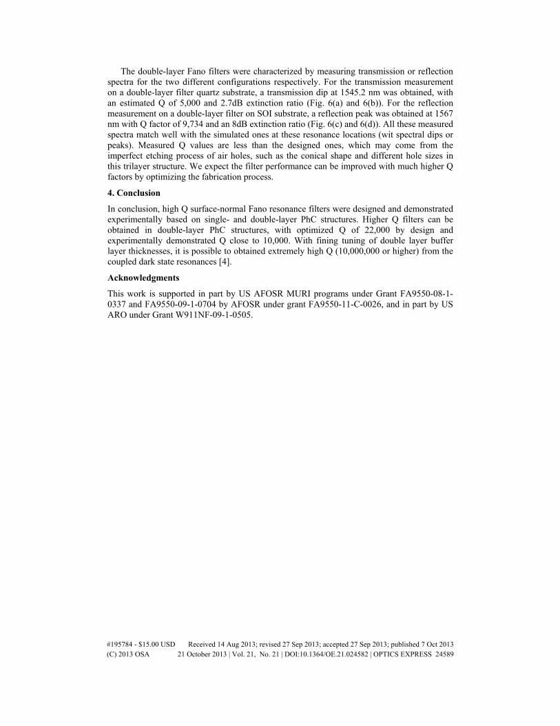
The double-layer Fano filters were characterized by measuring transmission or reflection spectra for the two different configurations respectively. For the transmission measurement on a double-layer filter quartz substrate, a transmission dip at 1545.2 nm was obtained, with an estimated Q of 5,000 and 2.7dB extinction ratio (Fig. 6(a) and 6(b)). For the reflection measurement on a double-layer filter on SOI substrate, a reflection peak was obtained at 1567 nm with Q factor of 9,734 and an 8dB extinction ratio (Fig. 6(c) and 6(d)). All these measured spectra match well with the simulated ones at these resonance locations (wit spectral dips or peaks). Measured Q values are less than the designed ones, which may come from the imperfect etching process of air holes, such as the conical shape and different hole sizes in this trilayer structure. We expect the filter performance can be improved with much higher Q factors by optimizing the fabrication process.
4. Conclusion
In conclusion, high Q surface-normal Fano resonance filters were designed and demonstrated experimentally based on single- and double-layer PhC structures. Higher Q filters can be obtained in double-layer PhC structures, with optimized Q of 22,000 by design and experimentally demonstrated Q close to 10,000. With fining tuning of double layer buffer layer thicknesses, it is possible to obtained extremely high Q (10,000,000 or higher) from the coupled dark state resonances [4].
Acknowledgments
This work is supported in part by US AFOSR MURI programs under Grant FA9550-08-1-0337 and FA9550-09-1-0704 by AFOSR under grant FA9550-11-C-0026, and in part by US ARO under Grant W911NF-09-1-0505.
#195784 - $15.00 USD Received 14 Aug 2013; revised 27 Sep 2013; accepted 27 Sep 2013; published 7 Oct 2013(C) 2013 OSA 21 October 2013 | Vol. 21, No. 21 | DOI:10.1364/OE.21.024582 | OPTICS EXPRESS 24589