Embed Size (px)
Citation preview
December 2007 Rev 5 1/34
34
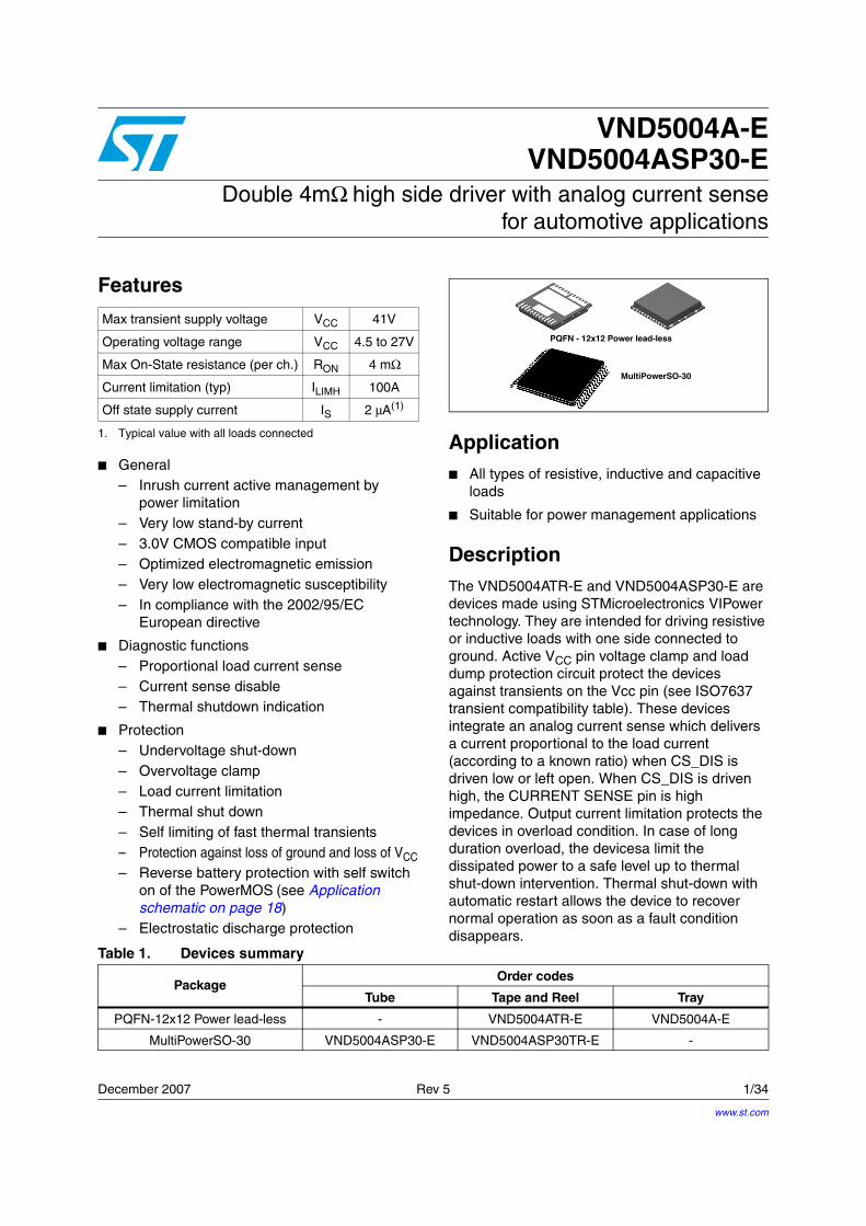
VND5004A-EVND5004ASP30-E
Double 4mΩ high side driver with analog current sensefor automotive applications
Features
General– Inrush current active management by
power limitation– Very low stand-by current– 3.0V CMOS compatible input– Optimized electromagnetic emission– Very low electromagnetic susceptibility– In compliance with the 2002/95/EC
European directive
Diagnostic functions– Proportional load current sense– Current sense disable– Thermal shutdown indication
Protection– Undervoltage shut-down– Overvoltage clamp– Load current limitation– Thermal shut down– Self limiting of fast thermal transients– Protection against loss of ground and loss of VCC– Reverse battery protection with self switch
on of the PowerMOS (see Application schematic on page 18)
– Electrostatic discharge protection
Application All types of resistive, inductive and capacitive
loads
Suitable for power management applications
DescriptionThe VND5004ATR-E and VND5004ASP30-E are devices made using STMicroelectronics VIPower technology. They are intended for driving resistive or inductive loads with one side connected to ground. Active VCC pin voltage clamp and load dump protection circuit protect the devices against transients on the Vcc pin (see ISO7637 transient compatibility table). These devices integrate an analog current sense which delivers a current proportional to the load current (according to a known ratio) when CS_DIS is driven low or left open. When CS_DIS is driven high, the CURRENT SENSE pin is high impedance. Output current limitation protects the devices in overload condition. In case of long duration overload, the devicesa limit the dissipated power to a safe level up to thermal shut-down intervention. Thermal shut-down with automatic restart allows the device to recover normal operation as soon as a fault condition disappears.
Max transient supply voltage VCC 41V
Operating voltage range VCC 4.5 to 27V
Max On-State resistance (per ch.) RON 4 mΩ
Current limitation (typ) ILIMH 100A
Off state supply current IS 2 µA(1)
1. Typical value with all loads connected
MultiPowerSO-30
PQFN - 12x12 Power lead-less
Table 1. Devices summary
PackageOrder codes
Tube Tape and Reel Tray
PQFN-12x12 Power lead-less - VND5004ATR-E VND5004A-E
MultiPowerSO-30 VND5004ASP30-E VND5004ASP30TR-E -
www.st.com
Contents VND5004A-E / VND5004ASP30-E
2/34
Contents
1 Block diagram and pin configurations . . . . . . . . . . . . . . . . . . . . . . . . . . 5
2 Electrical specifications . . . . . . . . . . . . . . . . . . . . . . . . . . . . . . . . . . . . . . 7
2.1 Absolute maximum ratings . . . . . . . . . . . . . . . . . . . . . . . . . . . . . . . . . . . . . 7
2.2 Thermal data . . . . . . . . . . . . . . . . . . . . . . . . . . . . . . . . . . . . . . . . . . . . . . . 8
2.3 Electrical characteristics . . . . . . . . . . . . . . . . . . . . . . . . . . . . . . . . . . . . . . . 9
2.4 Electrical characteristics curves . . . . . . . . . . . . . . . . . . . . . . . . . . . . . . . . 15
3 Application information . . . . . . . . . . . . . . . . . . . . . . . . . . . . . . . . . . . . . 18
3.1 MCU I/Os protection . . . . . . . . . . . . . . . . . . . . . . . . . . . . . . . . . . . . . . . . . 18
3.2 Load dump protection . . . . . . . . . . . . . . . . . . . . . . . . . . . . . . . . . . . . . . . . 18
3.3 Maximum demagnetization energy (VCC = 13.5V) . . . . . . . . . . . . . . . . . 19
4 Package and PC board thermal data . . . . . . . . . . . . . . . . . . . . . . . . . . . 20
4.1 MultiPowerSO-30 thermal data . . . . . . . . . . . . . . . . . . . . . . . . . . . . . . . . 20
4.2 PQFN - 12x12 Power lead-less thermal data . . . . . . . . . . . . . . . . . . . . . . 23
5 Package and packing information . . . . . . . . . . . . . . . . . . . . . . . . . . . . . 26
5.1 ECOPACK® packages . . . . . . . . . . . . . . . . . . . . . . . . . . . . . . . . . . . . . . . 26
5.2 MultiPowerSO-30 mechanical data . . . . . . . . . . . . . . . . . . . . . . . . . . . . . 26
5.3 PQFN - 12x12 Power lead-less mechanical data . . . . . . . . . . . . . . . . . . . 28
5.4 MultiPowerSO-30 packing information . . . . . . . . . . . . . . . . . . . . . . . . . . . 30
5.5 PQFN - 12x12 Power lead-less packing information . . . . . . . . . . . . . . . . 31
6 Revision history . . . . . . . . . . . . . . . . . . . . . . . . . . . . . . . . . . . . . . . . . . . 33
VND5004A-E / VND5004ASP30-E List of tables
3/34
List of tables
Table 1. Devices summary . . . . . . . . . . . . . . . . . . . . . . . . . . . . . . . . . . . . . . . . . . . . . . . . . . . . . . . . . 1Table 2. Pin functions . . . . . . . . . . . . . . . . . . . . . . . . . . . . . . . . . . . . . . . . . . . . . . . . . . . . . . . . . . . . . 5Table 3. Suggested connections for unused and n.c. pins . . . . . . . . . . . . . . . . . . . . . . . . . . . . . . . . . 6Table 4. Absolute maximum ratings . . . . . . . . . . . . . . . . . . . . . . . . . . . . . . . . . . . . . . . . . . . . . . . . . . 7Table 5. Thermal data. . . . . . . . . . . . . . . . . . . . . . . . . . . . . . . . . . . . . . . . . . . . . . . . . . . . . . . . . . . . . 8Table 6. Power section . . . . . . . . . . . . . . . . . . . . . . . . . . . . . . . . . . . . . . . . . . . . . . . . . . . . . . . . . . . . 9Table 7. Switching (VCC = 13V; Tj = 25°C) . . . . . . . . . . . . . . . . . . . . . . . . . . . . . . . . . . . . . . . . . . . . 9Table 8. Logic input . . . . . . . . . . . . . . . . . . . . . . . . . . . . . . . . . . . . . . . . . . . . . . . . . . . . . . . . . . . . . 10Table 9. Protection and diagnostics . . . . . . . . . . . . . . . . . . . . . . . . . . . . . . . . . . . . . . . . . . . . . . . . . 10Table 10. Current sense (8V<VCC<16V) . . . . . . . . . . . . . . . . . . . . . . . . . . . . . . . . . . . . . . . . . . . . . . 11Table 11. Truth table. . . . . . . . . . . . . . . . . . . . . . . . . . . . . . . . . . . . . . . . . . . . . . . . . . . . . . . . . . . . . . 12Table 12. Electrical transient requirements . . . . . . . . . . . . . . . . . . . . . . . . . . . . . . . . . . . . . . . . . . . . 13Table 13. Thermal parameters for MultiPowerSO-30 . . . . . . . . . . . . . . . . . . . . . . . . . . . . . . . . . . . . . 22Table 14. Thermal parameters for PQFN - 12x12 Power lead-less . . . . . . . . . . . . . . . . . . . . . . . . . . 25Table 15. MultiPowerSO-30 mechanical data . . . . . . . . . . . . . . . . . . . . . . . . . . . . . . . . . . . . . . . . . . 27Table 16. PQFN - 12x12 Power lead-less mechanical data . . . . . . . . . . . . . . . . . . . . . . . . . . . . . . . . 29Table 17. Document revision history . . . . . . . . . . . . . . . . . . . . . . . . . . . . . . . . . . . . . . . . . . . . . . . . . 33
List of figures VND5004A-E / VND5004ASP30-E
4/34
List of figures
Figure 1. Block diagram . . . . . . . . . . . . . . . . . . . . . . . . . . . . . . . . . . . . . . . . . . . . . . . . . . . . . . . . . . . . 5Figure 2. Configuration diagram (not in scale) . . . . . . . . . . . . . . . . . . . . . . . . . . . . . . . . . . . . . . . . . . 6Figure 3. Current and voltage conventions . . . . . . . . . . . . . . . . . . . . . . . . . . . . . . . . . . . . . . . . . . . . . 7Figure 4. Current sense delay characteristics . . . . . . . . . . . . . . . . . . . . . . . . . . . . . . . . . . . . . . . . . . 11Figure 5. Switching characteristics . . . . . . . . . . . . . . . . . . . . . . . . . . . . . . . . . . . . . . . . . . . . . . . . . . 12Figure 6. Waveforms . . . . . . . . . . . . . . . . . . . . . . . . . . . . . . . . . . . . . . . . . . . . . . . . . . . . . . . . . . . . . 14Figure 7. Off state output current . . . . . . . . . . . . . . . . . . . . . . . . . . . . . . . . . . . . . . . . . . . . . . . . . . . . 15Figure 8. High level input current . . . . . . . . . . . . . . . . . . . . . . . . . . . . . . . . . . . . . . . . . . . . . . . . . . . . 15Figure 9. Input clamp voltage. . . . . . . . . . . . . . . . . . . . . . . . . . . . . . . . . . . . . . . . . . . . . . . . . . . . . . . 15Figure 10. Input low level . . . . . . . . . . . . . . . . . . . . . . . . . . . . . . . . . . . . . . . . . . . . . . . . . . . . . . . . . . . 15Figure 11. Input high level . . . . . . . . . . . . . . . . . . . . . . . . . . . . . . . . . . . . . . . . . . . . . . . . . . . . . . . . . . 15Figure 12. Input hysteresis voltage . . . . . . . . . . . . . . . . . . . . . . . . . . . . . . . . . . . . . . . . . . . . . . . . . . . 15Figure 13. On state resistance vs. Tcase . . . . . . . . . . . . . . . . . . . . . . . . . . . . . . . . . . . . . . . . . . . . . 16Figure 14. On state resistance vs. VCC . . . . . . . . . . . . . . . . . . . . . . . . . . . . . . . . . . . . . . . . . . . . . . 16Figure 15. Undervoltage shutdown . . . . . . . . . . . . . . . . . . . . . . . . . . . . . . . . . . . . . . . . . . . . . . . . . . . 16Figure 16. Turn-On voltage slope . . . . . . . . . . . . . . . . . . . . . . . . . . . . . . . . . . . . . . . . . . . . . . . . . . . . 16Figure 17. ILIMH vs. Tcase . . . . . . . . . . . . . . . . . . . . . . . . . . . . . . . . . . . . . . . . . . . . . . . . . . . . . . . . 16Figure 18. Turn-Off voltage slope . . . . . . . . . . . . . . . . . . . . . . . . . . . . . . . . . . . . . . . . . . . . . . . . . . . . 16Figure 19. CS_DIS high level voltage . . . . . . . . . . . . . . . . . . . . . . . . . . . . . . . . . . . . . . . . . . . . . . . . . 17Figure 20. CS_DIS clamp voltage . . . . . . . . . . . . . . . . . . . . . . . . . . . . . . . . . . . . . . . . . . . . . . . . . . . . 17Figure 21. CS_DIS low level voltage . . . . . . . . . . . . . . . . . . . . . . . . . . . . . . . . . . . . . . . . . . . . . . . . . . 17Figure 22. Application schematic . . . . . . . . . . . . . . . . . . . . . . . . . . . . . . . . . . . . . . . . . . . . . . . . . . . . . 18Figure 23. Maximum turn off current versus inductance . . . . . . . . . . . . . . . . . . . . . . . . . . . . . . . . . . . 19Figure 24. MultiPowerSO-30 PC board . . . . . . . . . . . . . . . . . . . . . . . . . . . . . . . . . . . . . . . . . . . . . . . . 20Figure 25. Rthj-amb Vs. PCB copper area in open box free air condition (one channel ON) . . . . . . . 20Figure 26. MultiPowerSO-30 thermal impedance junction ambient single pulse (one channel ON) . . 21Figure 27. Thermal fitting model of a double channel HSD in MultiPowerSO-30 . . . . . . . . . . . . . . . . 21Figure 28. 12x12 Power lead-less package PC board. . . . . . . . . . . . . . . . . . . . . . . . . . . . . . . . . . . . . 23Figure 29. Rthj-amb Vs. PCB copper area in open box free air condition (one channel ON) . . . . . . . 23Figure 30. PQFN - 12x12 Power lead-less package thermal impedance junction ambient single pulse (one channel ON) . . . . . . . . . . . . . . . . . . . . . . . . . . . . . . . . . . . . . . . . . . . . . . . . . . . . . . . . . . . . . . . . . . . . . . . . . . . .24Figure 31. Thermal fitting model of a double channel HSD in PQFN - 12x12 Power lead-less . . . . . 24Figure 32. MultiPowerSO-30 outline . . . . . . . . . . . . . . . . . . . . . . . . . . . . . . . . . . . . . . . . . . . . . . . . . . 26Figure 33. PQFN - 12x12 Power lead-less outline. . . . . . . . . . . . . . . . . . . . . . . . . . . . . . . . . . . . . . . . 28Figure 34. MultiPowerSO-30 tube shipment (no suffix) . . . . . . . . . . . . . . . . . . . . . . . . . . . . . . . . . . . 30Figure 35. MultiPowerSO-30 tape and reel shipment (suffix “TR”) . . . . . . . . . . . . . . . . . . . . . . . . . . . 30Figure 36. PQFN - 12x12 Power lead-less tray shipment (no suffix) . . . . . . . . . . . . . . . . . . . . . . . . . . 31Figure 37. PQFN - 12x12 Power lead-less tape and reel shipment (suffix “TR”). . . . . . . . . . . . . . . . . 32
VND5004A-E / VND5004ASP30-E Block diagram and pin configurations
5/34
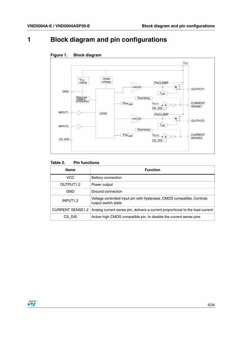
1 Block diagram and pin configurations
Figure 1. Block diagram
Table 2. Pin functions
Name Function
VCC Battery connection
OUTPUT1,2 Power output
GND Ground connection
INPUT1,2Voltage controlled input pin with hysteresis, CMOS compatible. Controls output switch state
CURRENT SENSE1,2 Analog current sense pin, delivers a current proportional to the load current
CS_DIS Active high CMOS compatible pin, to disable the current sense pins
PwCLAMP
IOUT1
GND
INPUT2
VCC
OUTPUT1
CURRENTSENSE1
CS_DIS
INPUT1
Undervoltage
VCCclamp
ILIM
Overtemp.
DRIVER
PwrLIM
PwCLAMP
KIOUT2
OUTPUT2
CURRENTSENSE2
ILIM
DRIVER
PwrLIM
CS_DIS
CS_DISK
Reversebatteryprotection
LOGIC
Overtemp.
Block diagram and pin configurations VND5004A-E / VND5004ASP30-E
6/34
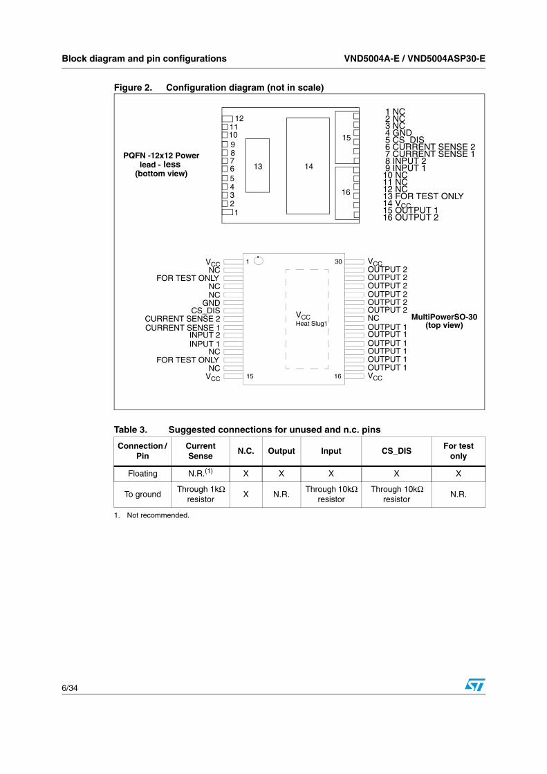
Figure 2. Configuration diagram (not in scale)
Table 3. Suggested connections for unused and n.c. pins
Connection / Pin
Current Sense
N.C. Output Input CS_DISFor test
only
Floating N.R.(1)
1. Not recommended.
X X X X X
To groundThrough 1kΩ
resistorX N.R.
Through 10kΩ resistor
Through 10kΩ resistor
N.R.
1 NC 2 NC 3 NC 4 GND 5 CS_DIS 6 CURRENT SENSE 2 7 CURRENT SENSE 1 8 INPUT 2 9 INPUT 110 NC11 NC12 NC13 FOR TEST ONLY14 VCC15 OUTPUT 116 OUTPUT 2
VCC
OUTPUT 2
VCC
OUTPUT 1
OUTPUT 2
OUTPUT 1
OUTPUT 2OUTPUT 2OUTPUT 2
OUTPUT 2NCOUTPUT 1
OUTPUT 1OUTPUT 1OUTPUT 1
1
15 16
30
MultiPowerSO-30
VCC
GND
VCC
INPUT 2
NC
NC
FOR TEST ONLYNCNC
CS_DISCURRENT SENSE 2CURRENT SENSE 1
INPUT 1NC
FOR TEST ONLY
VCCHeat Slug1 (top view)
PQFN -12x12 Powerless
(bottom view) lead -
121110987654321
13 14
15
16
VND5004A-E / VND5004ASP30-E Electrical specifications
7/34
2 Electrical specifications
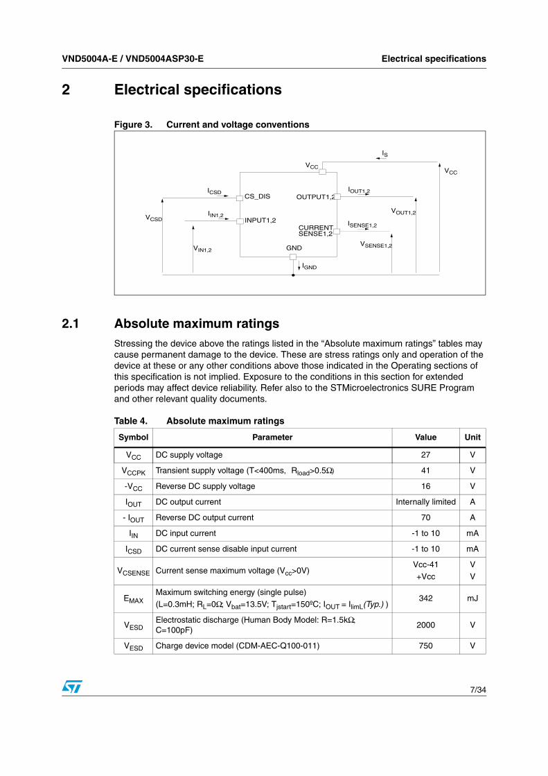
Figure 3. Current and voltage conventions
2.1 Absolute maximum ratingsStressing the device above the ratings listed in the “Absolute maximum ratings” tables may cause permanent damage to the device. These are stress ratings only and operation of the device at these or any other conditions above those indicated in the Operating sections of this specification is not implied. Exposure to the conditions in this section for extended periods may affect device reliability. Refer also to the STMicroelectronics SURE Program and other relevant quality documents.
IS
IGND
VCCVCC
VSENSE1,2
OUTPUT1,2IOUT1,2
CURRENTISENSE1,2
INPUT1,2IIN1,2
VIN1,2
VOUT1,2
GND
CS_DISICSD
VCSD
SENSE1,2
Table 4. Absolute maximum ratings
Symbol Parameter Value Unit
VCC DC supply voltage 27 V
VCCPK Transient supply voltage (T<400ms, Rload>0.5Ω) 41 V
-VCC Reverse DC supply voltage 16 V
IOUT DC output current Internally limited A
- IOUT Reverse DC output current 70 A
IIN DC input current -1 to 10 mA
ICSD DC current sense disable input current -1 to 10 mA
VCSENSE Current sense maximum voltage (Vcc>0V)Vcc-41
+Vcc
V
V
EMAXMaximum switching energy (single pulse)
(L=0.3mH; RL=0Ω; Vbat=13.5V; Tjstart=150ºC; IOUT = IlimL(Typ.) )342 mJ
VESDElectrostatic discharge (Human Body Model: R=1.5kΩ; C=100pF)
2000 V
VESD Charge device model (CDM-AEC-Q100-011) 750 V
Electrical specifications VND5004A-E / VND5004ASP30-E
8/34
2.2 Thermal data
Tj Junction operating temperature -40 to 150 °C
TSTG Storage temperature -55 to 150 °C
Table 4. Absolute maximum ratings (continued)
Symbol Parameter Value Unit
Table 5. Thermal data
Symbol ParameterValue
UnitMultiPowerSO-30 12x12 PLLP
Rthj-caseThermal resistance junction-case (MAX) (with one channel ON)
0.35 0.35 °C/W
Rthj-amb Thermal resistance junction-ambient (MAX) 58(1)
1. PCB FR4 area 58mmX58mm , PCB thickness 2mm, Cu thickness 35 µm, minimum pad layout.
39(2)
2. PCB FR4 area 78mmX78mm , PCB thickness 2mm, Cu thickness 35 µm, minimum pad layout.
°C/W
VND5004A-E / VND5004ASP30-E Electrical specifications
9/34
2.3 Electrical characteristicsValues specified in this section are for 8V<VCC<24V, -40°C<Tj<150 °C, unless otherwise stated.
Table 6. Power section
Symbol Parameter Test conditions Min. Typ. Max. Unit
VCCOperating supply voltage
4.5 13 27 V
VUSD Undervoltage shutdown 3.5 4.5 V
VUSDhystUndervoltage shut-down hysteresis
0.5 V
RON On-state resistance(1)
1. For each channel.
IOUT=15A; Tj=25°C
IOUT=15A; Tj=150°C
IOUT=15A; VCC=5V; Tj=25°C
4
8
6
mΩmΩmΩ
RON REVRdson in reverse battery condition
VCC=-13V; IOUT=-15A; Tj=25°C 4 mΩ
Vclamp VCC clamp voltage ICC=20 mA; IOUT1,2=0A 41 46 52 V
IS Supply currentOff state; VCC=13V; Tj=25°C; VIN=VOUT=VSENSE=VCSD=0V
On state; VCC=13V; VIN=5V; IOUT=0A2(2)
3.5
2. PowerMOS leakage included.
5(2)
6
µA
mA
IL(off)Off-state output current(1)
VIN=VOUT=0V; VCC=13V; Tj=25°C
VIN=VOUT=0V; VCC=13V; Tj=125°C
0
0
0.01 3
5µA
Table 7. Switching (VCC = 13V; Tj = 25°C)
Symbol Parameter Test conditions Min. Typ. Max. Unit
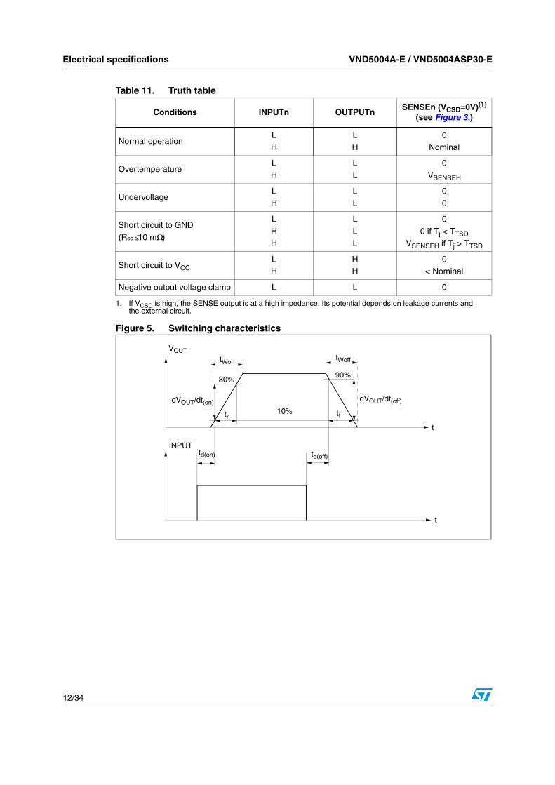
td(on) Turn-on delay time RL=0.87Ω (see Figure 5.) 25 µs
td(off) Turn-on delay time RL=0.87Ω (see Figure 5.) 35 µs
(dVOUT/dt)on Turn-on voltage slope RL=0.87ΩSee
Figure 16.
V/ µs
(dVOUT/dt)off Turn-off voltage slope RL=0.87ΩSee
Figure 18.
V/ µs
WONSwitching energy losses during twon
RL=0.87Ω (see Figure 5.) 5.4 mJ
WOFFSwitching energy losses during twoff
RL=0.87Ω (see Figure 5.) 2.3 mJ
Electrical specifications VND5004A-E / VND5004ASP30-E
10/34
Table 8. Logic input
Symbol Parameter Test conditions Min. Typ. Max. Unit
VIL1,2 Input low level voltage 0.9 V
IIL1,2 Low level input current VIN=0.9V 1 µA
VIH1,2 Input high level voltage 2.1 V
IIH1,2 High level input current VIN=2.1V 10 µA
VI(hyst)1,2Input hysteresis voltage
0.25 V
VICL1,2 Input clamp voltageIIN=1mAIIN=-1mA
5.5-0.7
7 VV
VCSDLCS_DIS low level voltage
0.9 V
ICSDLLow level CS_DIS current
VCSD=0.9V 1 µA
VCSDHCS_DIS high level voltage
2.1 V
ICSDHHigh level CS_DIS current
VCSD=2.1V 10 µA
VCSD(hyst)CS_DIS hysteresis voltage
0.25 V
VCSCL CS_DIS clamp voltageICSD=1mA
ICSD=-1mA
5.5
-0.7
7 V
V
Table 9. Protection and diagnostics(1)
1. To ensure long term reliability under heavy overload or short circuit conditions, protection and related diagnostic signals must be used together with a proper software strategy. If the device is subjected to abnormal conditions, this software must limit the duration and number of activation cycles.
Symbol Parameter Test conditions Min. Typ. Max. Unit
IlimH Short circuit currentVCC=13V
5V<VCC<24V
70 100 140
140
A
A
IlimL
Short circuit current during thermal cycling
VCC=13V; TR<Tj<TTSD 40 A
TTSDShutdown temperature
150 175 200 °C
TR Reset temperature TRS+1 TRS+5 °C
TRSThermal reset of STATUS
135 °C
THYSTThermal hysteresis (TTSD-TR)
7 °C
VDEMAGTurn-off output voltage clamp
IOUT=2A; VIN=0; L=6mH VCC-27 VCC-30 VCC-33 V
VND5004A-E / VND5004ASP30-E Electrical specifications
11/34
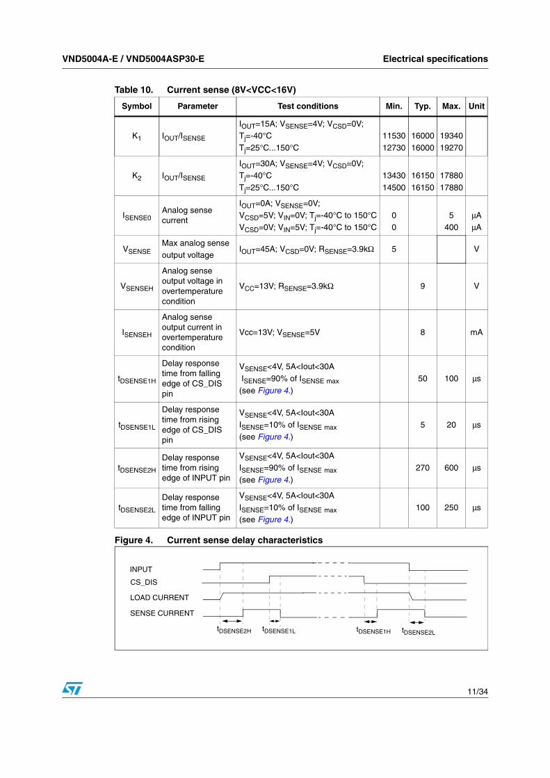
Figure 4. Current sense delay characteristics
Table 10. Current sense (8V<VCC<16V)
Symbol Parameter Test conditions Min. Typ. Max. Unit
K1 IOUT/ISENSE
IOUT=15A; VSENSE=4V; VCSD=0V;Tj=-40°C
Tj=25°C...150°C
11530
12730
16000
16000
19340
19270
K2 IOUT/ISENSE
IOUT=30A; VSENSE=4V; VCSD=0V;
Tj=-40°C
Tj=25°C...150°C
13430
14500
16150
16150
17880
17880
ISENSE0Analog sense current
IOUT=0A; VSENSE=0V;
VCSD=5V; VIN=0V; Tj=-40°C to 150°CVCSD=0V; VIN=5V; Tj=-40°C to 150°C
00
5400
µAµA
VSENSEMax analog sense output voltage
IOUT=45A; VCSD=0V; RSENSE=3.9kΩ 5 V
VSENSEH
Analog sense output voltage in overtemperature condition
VCC=13V; RSENSE=3.9kΩ 9 V
ISENSEH
Analog sense output current in overtemperature condition
Vcc=13V; VSENSE=5V 8 mA
tDSENSE1H
Delay response time from falling edge of CS_DIS pin
VSENSE<4V, 5A<Iout<30A
ISENSE=90% of ISENSE max
(see Figure 4.)50 100 µs
tDSENSE1L
Delay response time from rising edge of CS_DIS pin
VSENSE<4V, 5A<Iout<30A
ISENSE=10% of ISENSE max
(see Figure 4.)
5 20 µs
tDSENSE2H
Delay response time from rising edge of INPUT pin
VSENSE<4V, 5A<Iout<30A
ISENSE=90% of ISENSE max
(see Figure 4.)
270 600 µs
tDSENSE2L
Delay response time from falling edge of INPUT pin
VSENSE<4V, 5A<Iout<30A
ISENSE=10% of ISENSE max
(see Figure 4.)100 250 µs
SENSE CURRENT
INPUT
LOAD CURRENT
CS_DIS
tDSENSE2H tDSENSE2LtDSENSE1L tDSENSE1H
Electrical specifications VND5004A-E / VND5004ASP30-E
12/34
Figure 5. Switching characteristics
Table 11. Truth table
Conditions INPUTn OUTPUTnSENSEn (VCSD=0V)(1)
(see Figure 3.)
1. If VCSD is high, the SENSE output is at a high impedance. Its potential depends on leakage currents and the external circuit.
Normal operationL
H
L
H
0
Nominal
OvertemperatureL
H
L
L
0
VSENSEH
UndervoltageL
H
L
L
0
0
Short circuit to GND
(Rsc ≤ 10 mΩ)
L
HH
L
LL
0
0 if Tj < TTSD
VSENSEH if Tj > TTSD
Short circuit to VCCLH
HH
0< Nominal
Negative output voltage clamp L L 0
VOUT
dVOUT/dt(on)
tr
80%
10% tf
dVOUT/dt(off)
td(off)td(on)
INPUT
t
t
90%
tWontWoff
VND5004A-E / VND5004ASP30-E Electrical specifications
13/34
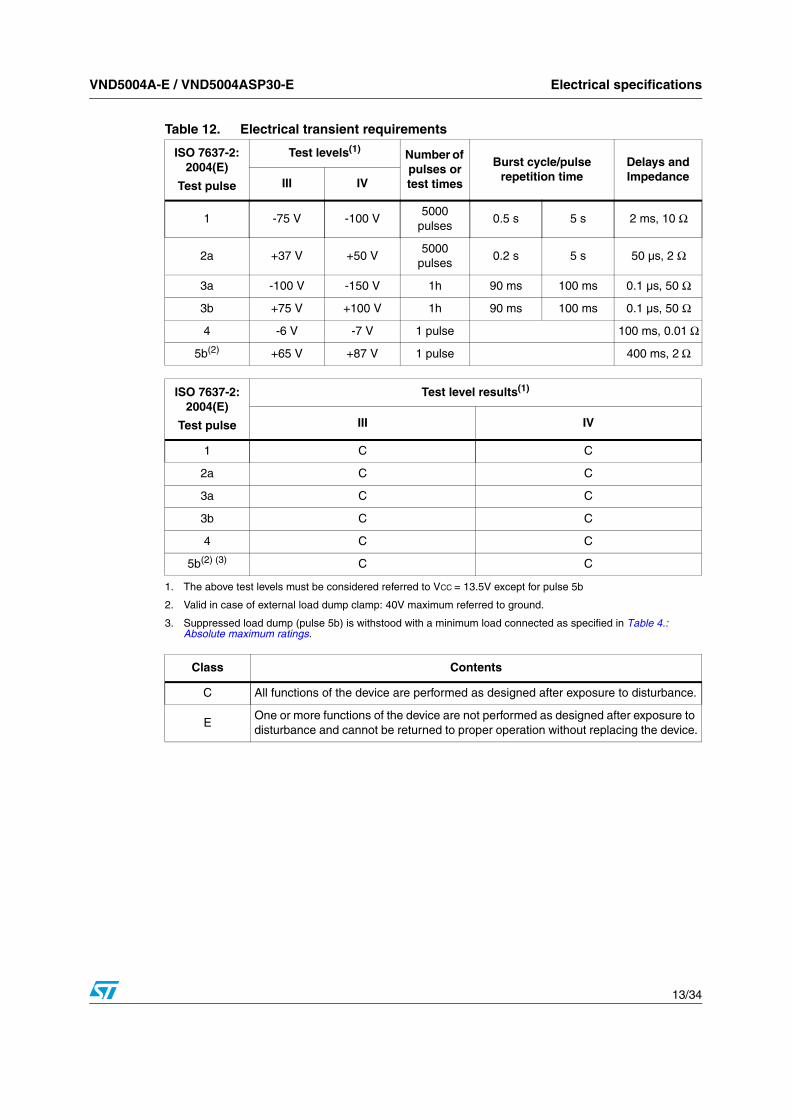
Table 12. Electrical transient requirements
ISO 7637-2: 2004(E)
Test pulse
Test levels(1) Number of pulses or test times
Burst cycle/pulse repetition time
Delays andImpedanceIII IV
1 -75 V -100 V5000
pulses0.5 s 5 s 2 ms, 10 Ω
2a +37 V +50 V5000
pulses0.2 s 5 s 50 µs, 2 Ω
3a -100 V -150 V 1h 90 ms 100 ms 0.1 µs, 50 Ω
3b +75 V +100 V 1h 90 ms 100 ms 0.1 µs, 50 Ω
4 -6 V -7 V 1 pulse 100 ms, 0.01 Ω
5b(2) +65 V +87 V 1 pulse 400 ms, 2 Ω
ISO 7637-2: 2004(E)
Test pulse
Test level results(1)
1. The above test levels must be considered referred to VCC = 13.5V except for pulse 5b
III IV
1 C C
2a C C
3a C C
3b C C
4 C C
5b(2) (3)
2. Valid in case of external load dump clamp: 40V maximum referred to ground.
3. Suppressed load dump (pulse 5b) is withstood with a minimum load connected as specified in Table 4.: Absolute maximum ratings.
C C
Class Contents
C All functions of the device are performed as designed after exposure to disturbance.
EOne or more functions of the device are not performed as designed after exposure to disturbance and cannot be returned to proper operation without replacing the device.
Electrical specifications VND5004A-E / VND5004ASP30-E
14/34
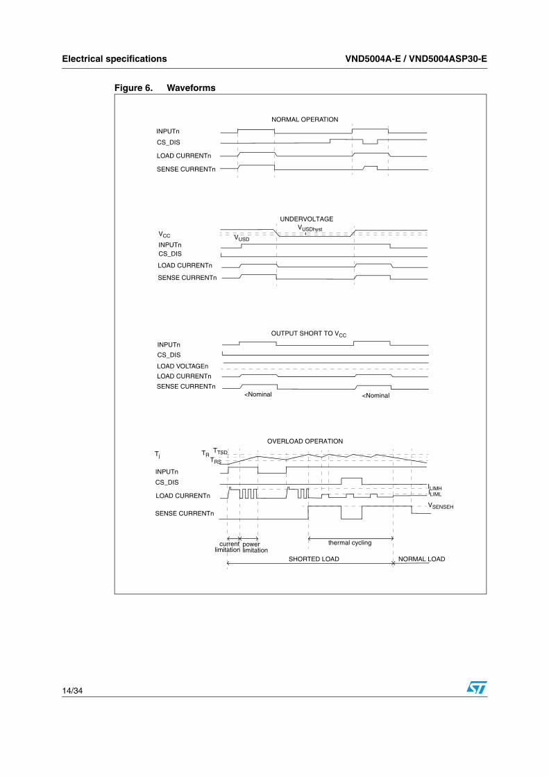
Figure 6. Waveforms
SENSE CURRENTn
INPUTn
NORMAL OPERATION
UNDERVOLTAGE
VCC VUSD
VUSDhyst
INPUTn
SENSE CURRENTn
LOAD CURRENTn
LOAD CURRENTn
OVERLOAD OPERATION
INPUTn
SENSE CURRENTn
TTSDTRTj
LOAD CURRENTn
INPUTn
LOAD VOLTAGEn
SENSE CURRENTn
LOAD CURRENTn
<Nominal <Nominal
OUTPUT SHORT TO VCC
CS_DIS
CS_DIS
CS_DIS
CS_DIS
TRS
ILIMHILIML
VSENSEH
thermal cyclingpowerlimitation
currentlimitation
SHORTED LOAD NORMAL LOAD
VND5004A-E / VND5004ASP30-E Electrical specifications
15/34
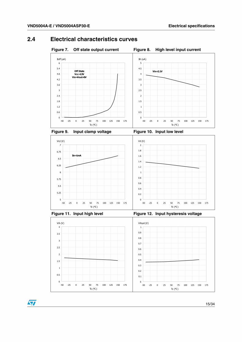
2.4 Electrical characteristics curves
Figure 7. Off state output current Figure 8. High level input current
Figure 9. Input clamp voltage Figure 10. Input low level
Figure 11. Input high level Figure 12. Input hysteresis voltage
-50 -25 0 25 50 75 100 125 150 175
Tc (°C)
0
0.6
1.2
1.8
2.4
3
3.6
4.2
4.8
5.4
6
Iloff (uA)
Off StateVcc=13V
Vin=Vout=0V
-50 -25 0 25 50 75 100 125 150 175
Tc (°C)
0
0.5
1
1.5
2
2.5
3
3.5
4
4.5
5
Iih (uA)
Vin=2.1V
-50 -25 0 25 50 75 100 125 150 175
Tc (°C)
5
5.25
5.5
5.75
6
6.25
6.5
6.75
7
Vicl (V)
Iin=1mA
-50 -25 0 25 50 75 100 125 150 175
Tc (°C)
0
0.2
0.4
0.6
0.8
1
1.2
1.4
1.6
1.8
2
Vil (V)
-50 -25 0 25 50 75 100 125 150 175
Tc (°C)
0
0.5
1
1.5
2
2.5
3
3.5
4
Vih (V)
-50 -25 0 25 50 75 100 125 150 175
Tc (°C)
0
0.1
0.2
0.3
0.4
0.5
0.6
0.7
0.8
0.9
1
Vihyst (V)
Electrical specifications VND5004A-E / VND5004ASP30-E
16/34
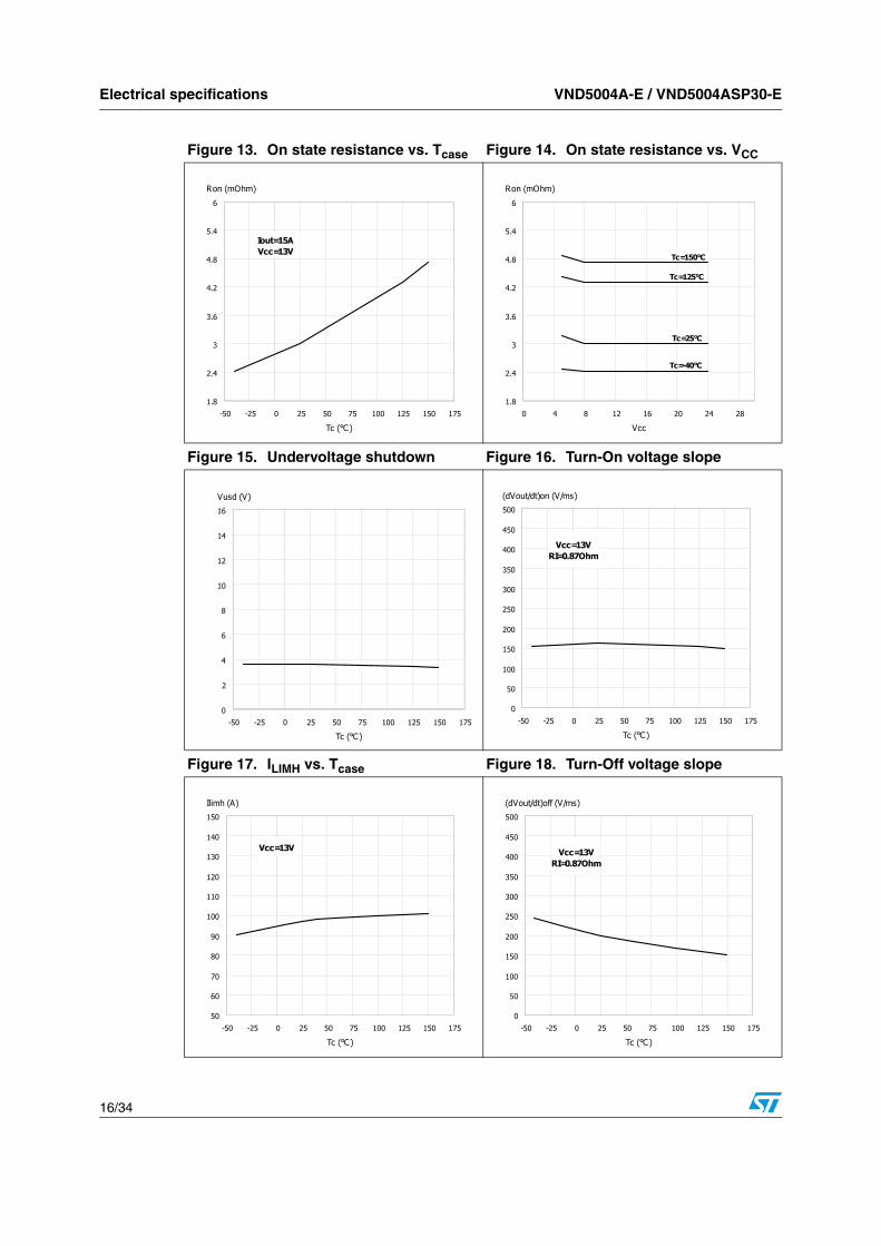
Figure 13. On state resistance vs. Tcase Figure 14. On state resistance vs. VCC
Figure 15. Undervoltage shutdown Figure 16. Turn-On voltage slope
Figure 17. ILIMH vs. Tcase Figure 18. Turn-Off voltage slope
-50 -25 0 25 50 75 100 125 150 175
Tc (°C)
1.8
2.4
3
3.6
4.2
4.8
5.4
6
Ron (mOhm)
Iout=15AVcc=13V
0 4 8 12 16 20 24 28
Vcc
1.8
2.4
3
3.6
4.2
4.8
5.4
6
Ron (mOhm)
Tc=150°C
Tc=125°C
Tc=25°C
Tc=-40°C
-50 -25 0 25 50 75 100 125 150 175
Tc (°C)
0
2
4
6
8
10
12
14
16
Vusd (V)
-50 -25 0 25 50 75 100 125 150 175
Tc (°C)
0
50
100
150
200
250
300
350
400
450
500
(dVout/dt)on (V/ms)
Vcc=13VRI=0.87Ohm
-50 -25 0 25 50 75 100 125 150 175
Tc (°C)
50
60
70
80
90
100
110
120
130
140
150
Ilimh (A)
Vcc=13V
-50 -25 0 25 50 75 100 125 150 175
Tc (°C)
0
50
100
150
200
250
300
350
400
450
500
(dVout/dt)off (V/ms)
Vcc=13VRI=0.87Ohm
VND5004A-E / VND5004ASP30-E Electrical specifications
17/34
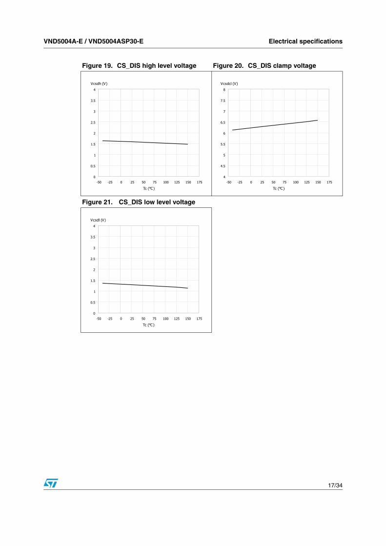
Figure 19. CS_DIS high level voltage Figure 20. CS_DIS clamp voltage
Figure 21. CS_DIS low level voltage
-50 -25 0 25 50 75 100 125 150 175
Tc (°C)
0
0.5
1
1.5
2
2.5
3
3.5
4
Vcsdh (V)
-50 -25 0 25 50 75 100 125 150 175
Tc (°C)
4
4.5
5
5.5
6
6.5
7
7.5
8
Vcsdcl (V)
-50 -25 0 25 50 75 100 125 150 175
Tc (°C)
0
0.5
1
1.5
2
2.5
3
3.5
4
Vcsdl (V)
Application information VND5004A-E / VND5004ASP30-E
18/34
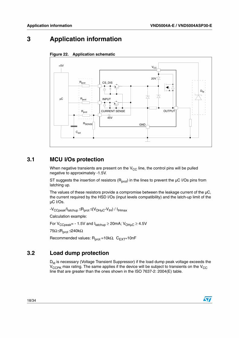
3 Application information
Figure 22. Application schematic
3.1 MCU I/Os protectionWhen negative transients are present on the VCC line, the control pins will be pulled negative to approximately -1.5V.
ST suggests the insertion of resistors (Rprot) in the lines to prevent the µC I/Os pins from latching up.
The values of these resistors provide a compromise between the leakage current of the µC, the current required by the HSD I/Os (input levels compatibility) and the latch-up limit of the µC I/Os.
-VCCpeak/Ilatchup ≤ Rprot ≤ (VOHµC-VIH) / IIHmax
Calculation example:
For VCCpeak= - 1.5V and Ilatchup ≥ 20mA; VOHµC ≥ 4.5V
75Ω ≤ Rprot ≤ 240kΩ.
Recommended values: Rprot =10kΩ, CEXT=10nF
3.2 Load dump protection Dld is necessary (Voltage Transient Suppressor) if the load dump peak voltage exceeds the VCCPK max rating. The same applies if the device will be subject to transients on the VCC line that are greater than the ones shown in the ISO 7637-2: 2004(E) table.
VCC
GND
OUTPUT
+5V
CS_DIS
INPUTRprot
Rprot
20V
Dld
Rprot
RSENSE
CURRENT SENSE
µC
45V
Cext
VND5004A-E / VND5004ASP30-E Application information
19/34
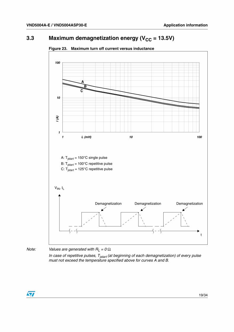
3.3 Maximum demagnetization energy (VCC = 13.5V)
Figure 23. Maximum turn off current versus inductance
Note: Values are generated with RL = 0 Ω.In case of repetitive pulses, Tjstart (at beginning of each demagnetization) of every pulse must not exceed the temperature specified above for curves A and B.
1
10
100
1 10 100L (mH)
I (A
)
Demagnetization Demagnetization Demagnetization
t
VIN, IL
C: Tjstart = 125°C repetitive pulse
A: Tjstart = 150°C single pulse
B: Tjstart = 100°C repetitive pulse
AB
C
Package and PC board thermal data VND5004A-E / VND5004ASP30-E
20/34
4 Package and PC board thermal data
4.1 MultiPowerSO-30 thermal data
Figure 24. MultiPowerSO-30 PC board
Note: Layout condition of Rth and Zth measurements (PCB: Double layer, Thermal Vias, FR4 area= 58mm x 58mm, PCB thickness=2mm, Cu thickness=35µm (front and back side), Copper areas: from minimum pad lay-out to 16cm2).
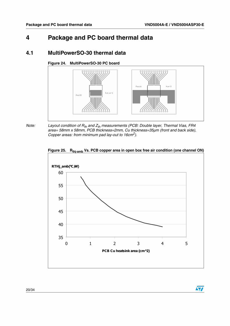
Figure 25. Rthj-amb Vs. PCB copper area in open box free air condition (one channel ON)
35
40
45
50
55
60
0 1 2 3 4 5
RTHj_amb(°C/W)
PCB Cu heatsink area (cm 2)
VND5004A-E / VND5004ASP30-E Package and PC board thermal data
21/34
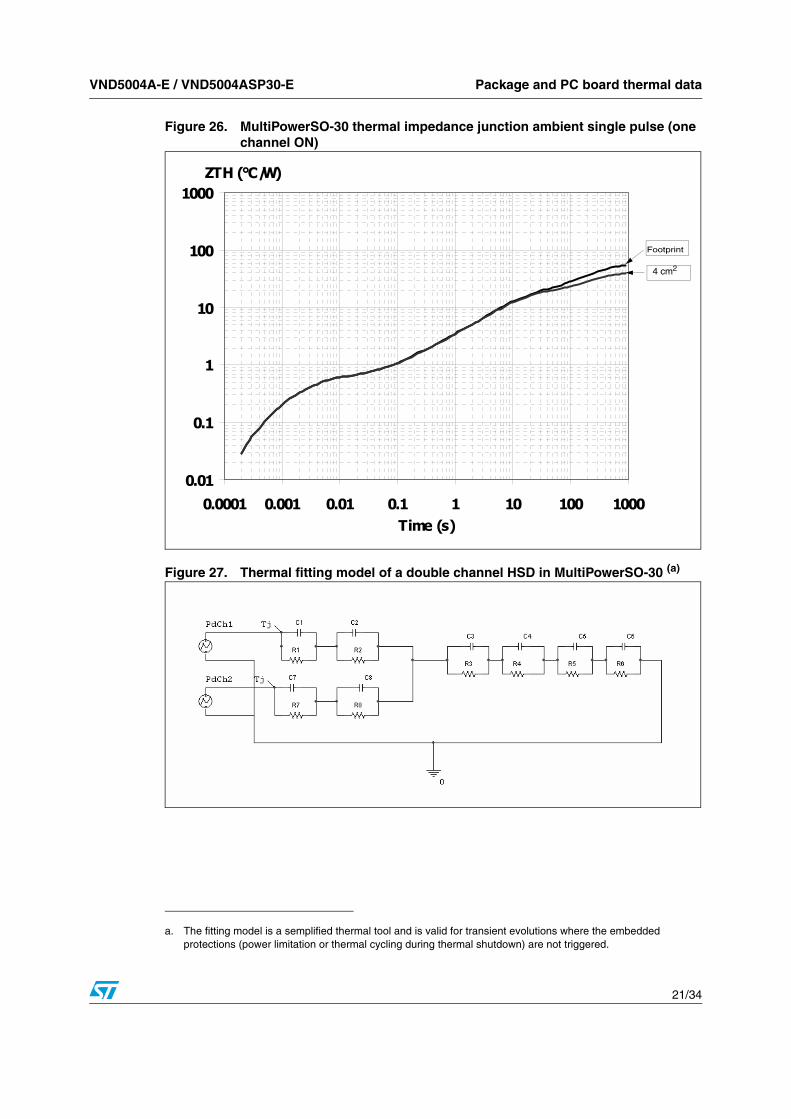
Figure 26. MultiPowerSO-30 thermal impedance junction ambient single pulse (one channel ON)
Figure 27. Thermal fitting model of a double channel HSD in MultiPowerSO-30 (a)
a. The fitting model is a semplified thermal tool and is valid for transient evolutions where the embedded protections (power limitation or thermal cycling during thermal shutdown) are not triggered.
0.01
0.1
1
10
100
1000
0.0001 0.001 0.01 0.1 1 10 100 1000Time (s)
ZTH (°C/W)
Footprint
4 cm2
Package and PC board thermal data VND5004A-E / VND5004ASP30-E
22/34
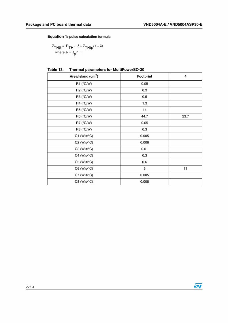
Equation 1: pulse calculation formula
Table 13. Thermal parameters for MultiPowerSO-30
Area/island (cm2) Footprint 4
R1 (°C/W) 0.05
R2 (°C/W) 0.3
R3 (°C/W) 0.5
R4 (°C/W) 1.3
R5 (°C/W) 14
R6 (°C/W) 44.7 23.7
R7 (°C/W) 0.05
R8 (°C/W) 0.3
C1 (W.s/°C) 0.005
C2 (W.s/°C) 0.008
C3 (W.s/°C) 0.01
C4 (W.s/°C) 0.3
C5 (W.s/°C) 0.6
C6 (W.s/°C) 5 11
C7 (W.s/°C) 0.005
C8 (W.s/°C) 0.008
ZTHδ RTH δ ZTHtp 1 δ–( )+⋅=
where δ tp T⁄=
VND5004A-E / VND5004ASP30-E Package and PC board thermal data
23/34
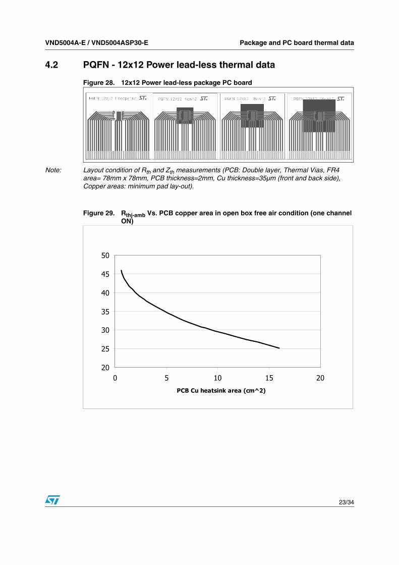
4.2 PQFN - 12x12 Power lead-less thermal data
Figure 28. 12x12 Power lead-less package PC board
Note: Layout condition of Rth and Zth measurements (PCB: Double layer, Thermal Vias, FR4 area= 78mm x 78mm, PCB thickness=2mm, Cu thickness=35µm (front and back side), Copper areas: minimum pad lay-out).
Figure 29. Rthj-amb Vs. PCB copper area in open box free air condition (one channel ON)
20
25
30
35
40
45
50
0 5 10 15 20
PCB Cu heatsink area (cm^2)
Package and PC board thermal data VND5004A-E / VND5004ASP30-E
24/34
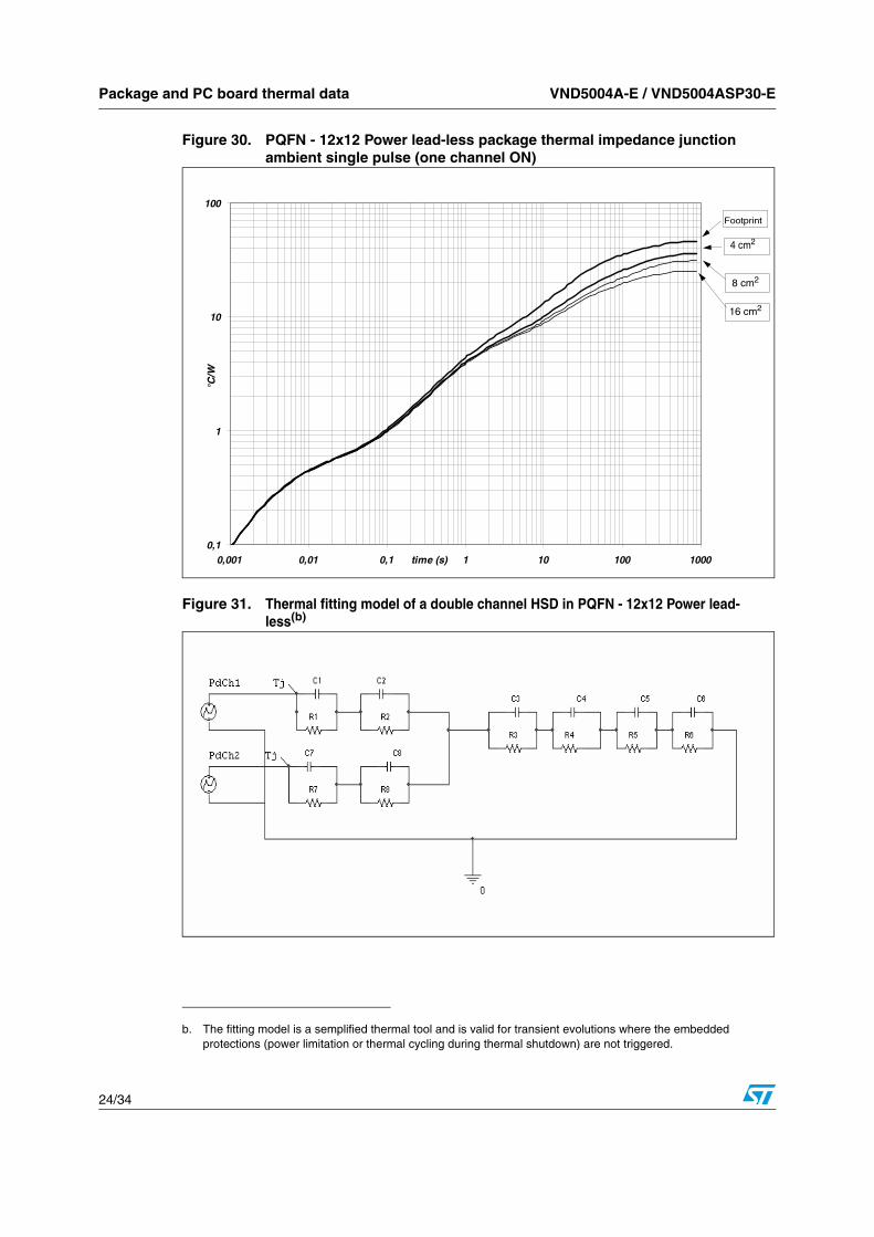
Figure 30. PQFN - 12x12 Power lead-less package thermal impedance junction ambient single pulse (one channel ON)
Figure 31. Thermal fitting model of a double channel HSD in PQFN - 12x12 Power lead-less(b)
b. The fitting model is a semplified thermal tool and is valid for transient evolutions where the embedded protections (power limitation or thermal cycling during thermal shutdown) are not triggered.
0,1
1
10
100
0,001 0,01 0,1 1 10 100 1000time (s)
°C/W
Footprint
4 cm2
8 cm2
16 cm2
VND5004A-E / VND5004ASP30-E Package and PC board thermal data
25/34
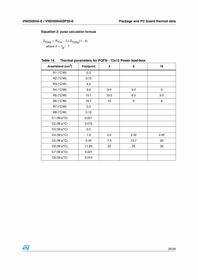
Equation 2: pulse calculation formula
Table 14. Thermal parameters for PQFN - 12x12 Power lead-less
Area/island (cm2) Footprint 4 8 16
R1 (°C/W) 0.3
R2 (°C/W) 0.15
R3 (°C/W) 4.2
R4 (°C/W) 9.6 9.4 9.2 9
R5 (°C/W) 15.1 10.5 8.5 5.5
R6 (°C/W) 16.7 12 9 6
R7 (°C/W) 0.3
R8 (°C/W) 0.15
C1 (W.s/°C) 0.021
C2 (W.s/°C) 0.015
C3 (W.s/°C) 0.2
C4 (W.s/°C) 1.9 2.2 2.32 2.45
C5 (W.s/°C) 2.45 7.3 13.7 20
C6 (W.s/°C) 11.85 22 25 30
C7 (W.s/°C) 0.021
C8 (W.s/°C) 0.015
ZTHδ RTH δ ZTHtp 1 δ–( )+⋅=
where δ tp T⁄=
Package and packing information VND5004A-E / VND5004ASP30-E
26/34
5 Package and packing information
5.1 ECOPACK® packagesIn order to meet environmental requirements, ST offers these devices in ECOPACK®
packages. ECOPACK® packages are lead-free. The category of Second Level Interconnect is marked on the package and on the inner box label, in compliance with JEDEC Standard JESD97. The maximum ratings related to soldering conditions are also marked on the inner box label.
ECOPACK is an ST trademark. ECOPACK specifications are available at www.st.com.
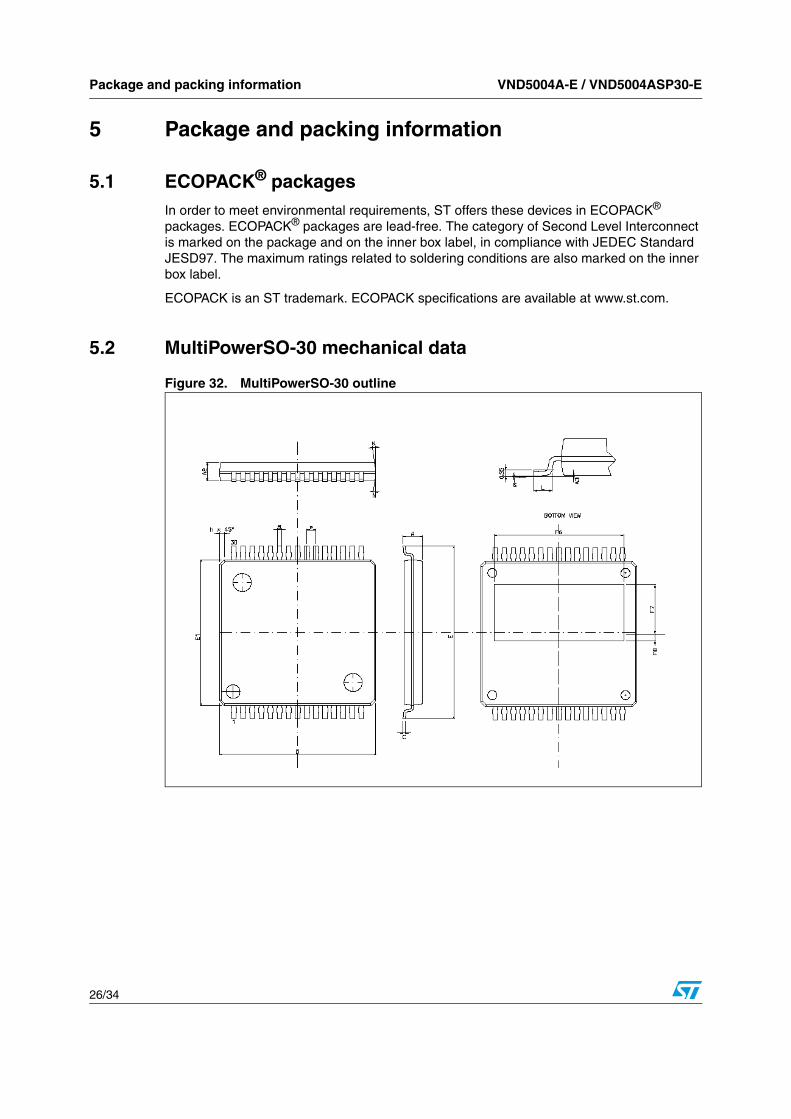
5.2 MultiPowerSO-30 mechanical data
Figure 32. MultiPowerSO-30 outline
VND5004A-E / VND5004ASP30-E Package and packing information
27/34
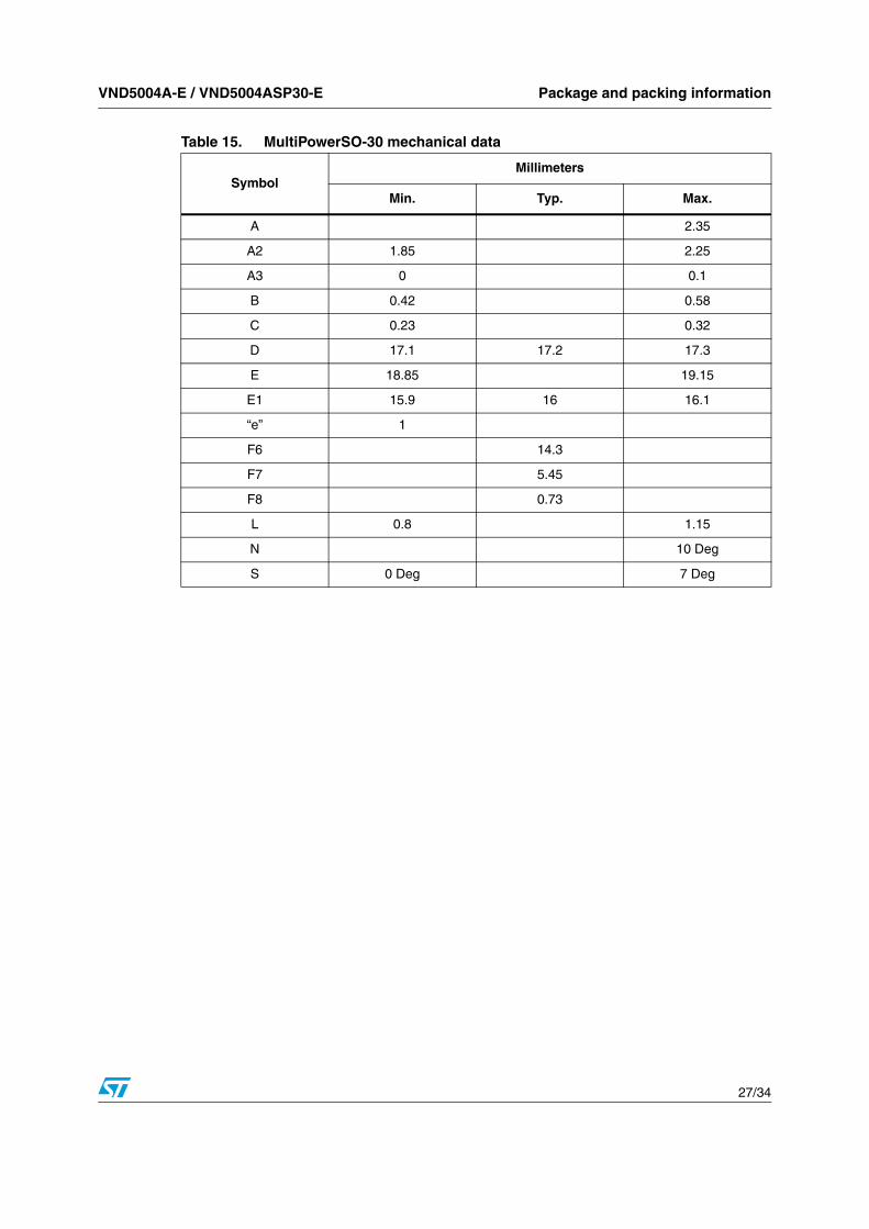
Table 15. MultiPowerSO-30 mechanical data
SymbolMillimeters
Min. Typ. Max.
A 2.35
A2 1.85 2.25
A3 0 0.1
B 0.42 0.58
C 0.23 0.32
D 17.1 17.2 17.3
E 18.85 19.15
E1 15.9 16 16.1
“e” 1
F6 14.3
F7 5.45
F8 0.73
L 0.8 1.15
N 10 Deg
S 0 Deg 7 Deg
Package and packing information VND5004A-E / VND5004ASP30-E
28/34
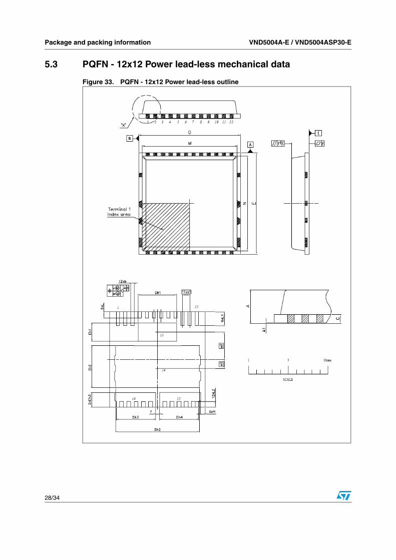
5.3 PQFN - 12x12 Power lead-less mechanical data
Figure 33. PQFN - 12x12 Power lead-less outline
VND5004A-E / VND5004ASP30-E Package and packing information
29/34
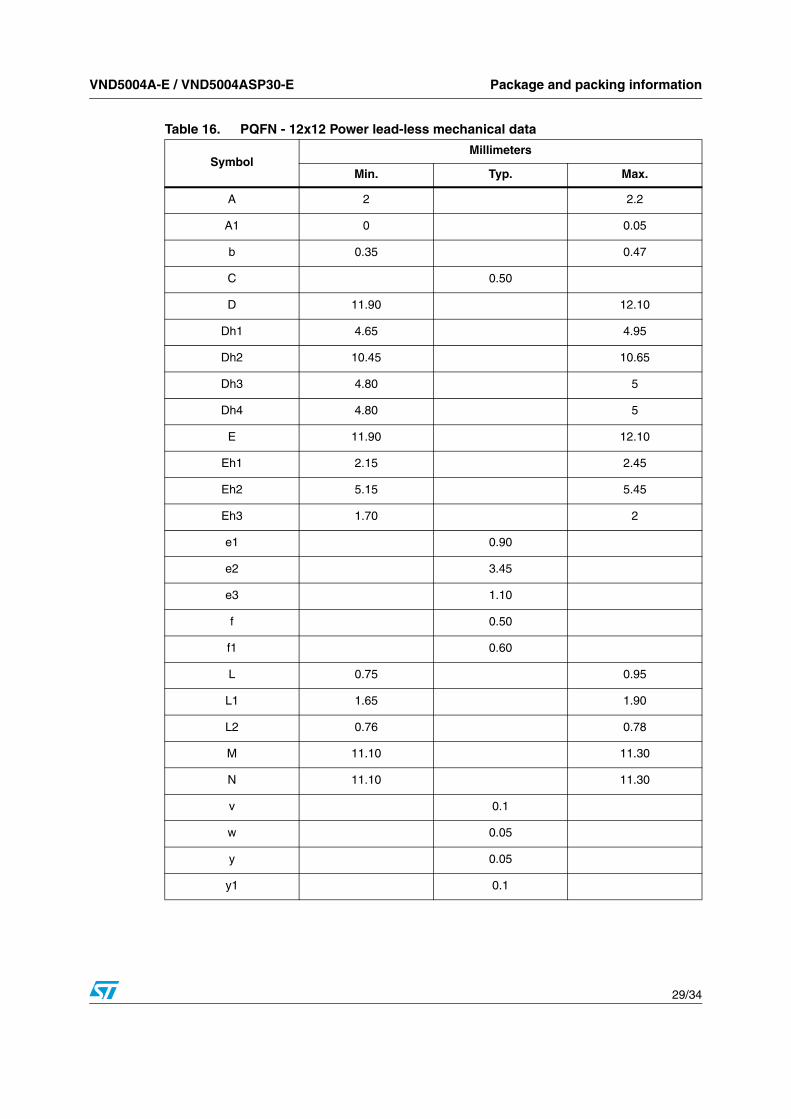
Table 16. PQFN - 12x12 Power lead-less mechanical data
SymbolMillimeters
Min. Typ. Max.
A 2 2.2
A1 0 0.05
b 0.35 0.47
C 0.50
D 11.90 12.10
Dh1 4.65 4.95
Dh2 10.45 10.65
Dh3 4.80 5
Dh4 4.80 5
E 11.90 12.10
Eh1 2.15 2.45
Eh2 5.15 5.45
Eh3 1.70 2
e1 0.90
e2 3.45
e3 1.10
f 0.50
f1 0.60
L 0.75 0.95
L1 1.65 1.90
L2 0.76 0.78
M 11.10 11.30
N 11.10 11.30
v 0.1
w 0.05
y 0.05
y1 0.1
Package and packing information VND5004A-E / VND5004ASP30-E
30/34
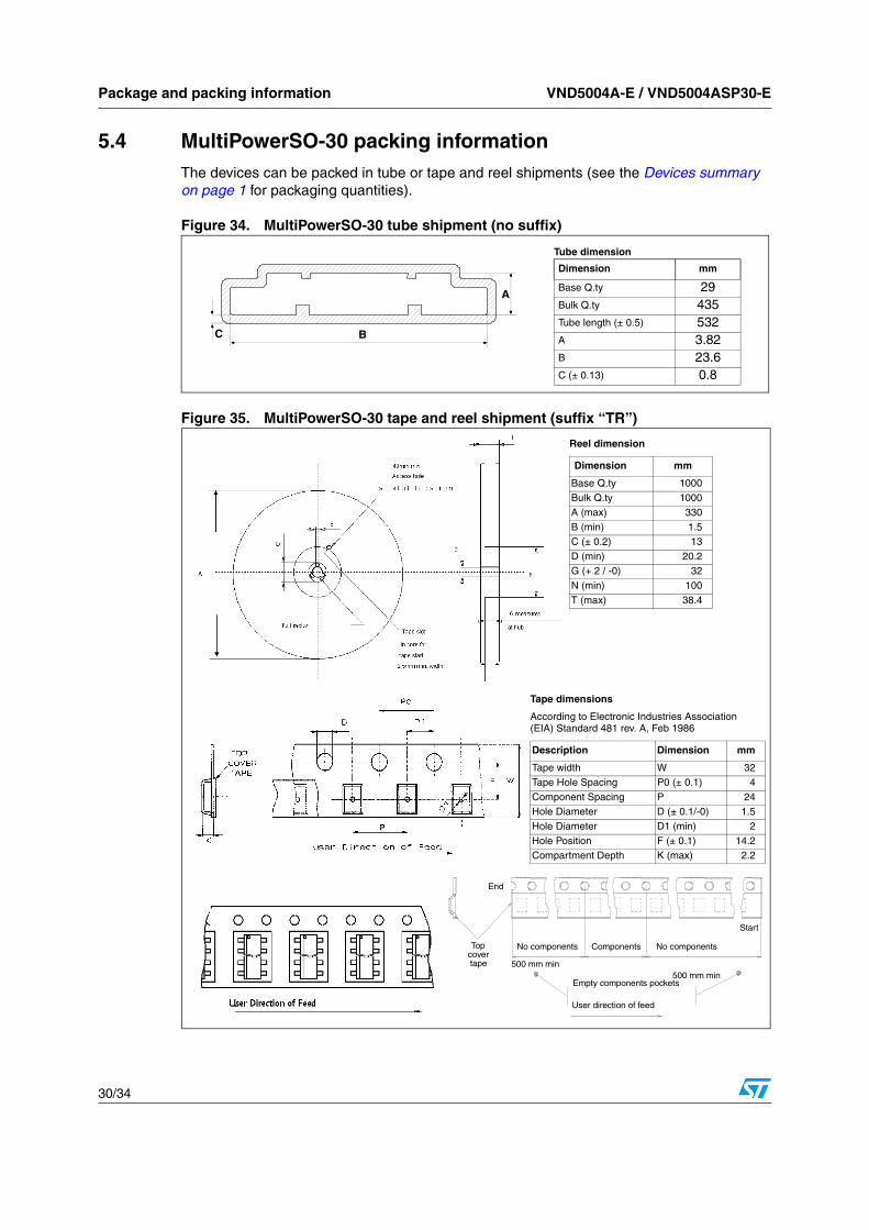
5.4 MultiPowerSO-30 packing informationThe devices can be packed in tube or tape and reel shipments (see the Devices summary on page 1 for packaging quantities).
Figure 34. MultiPowerSO-30 tube shipment (no suffix)
Figure 35. MultiPowerSO-30 tape and reel shipment (suffix “TR”)
A
BC
Tube dimension
Dimension mm
Base Q.ty 29Bulk Q.ty 435Tube length (± 0.5) 532A 3.82B 23.6C (± 0.13) 0.8
Reel dimension
Dimension mm
Base Q.ty 1000Bulk Q.ty 1000A (max) 330B (min) 1.5C (± 0.2) 13D (min) 20.2G (+ 2 / -0) 32N (min) 100T (max) 38.4
Topcovertape
Start
No componentsNo components Components
500 mm min500 mm min
Empty components pockets
User direction of feed
Tape dimensions
According to Electronic Industries Association (EIA) Standard 481 rev. A, Feb 1986
Description Dimension mm
Tape width W 32Tape Hole Spacing P0 (± 0.1) 4Component Spacing P 24Hole Diameter D (± 0.1/-0) 1.5Hole Diameter D1 (min) 2Hole Position F (± 0.1) 14.2Compartment Depth K (max) 2.2
End
VND5004A-E / VND5004ASP30-E Package and packing information
31/34
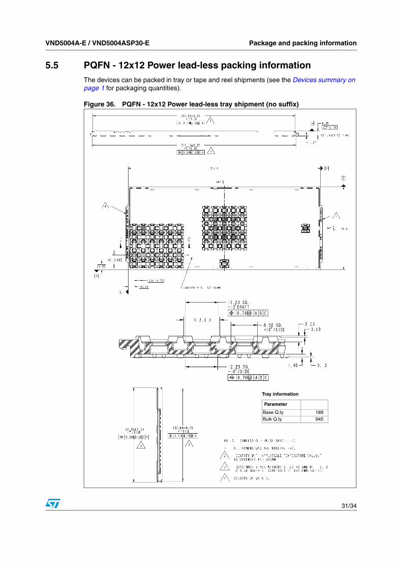
5.5 PQFN - 12x12 Power lead-less packing informationThe devices can be packed in tray or tape and reel shipments (see the Devices summary on page 1 for packaging quantities).
Figure 36. PQFN - 12x12 Power lead-less tray shipment (no suffix)
Tray information
Parameter
Base Q.ty 189Bulk Q.ty 945
Package and packing information VND5004A-E / VND5004ASP30-E
32/34
Figure 37. PQFN - 12x12 Power lead-less tape and reel shipment (suffix “TR”)
Tape dimensions
Dimension mm
A0 ± 0.1 12.30
B0 ± 0.1 12.30
K0 ± 0.1 2.15
F ± 0.1 11.50
E ± 0.1 1.75
W ± 0.3 24
P2 ± 0.1 2
P0 ± 0.1 4
P1 ± 0.1 16
T ± 0.05 0.30 D 1.50
D1 (min) 1.50
Reel dimensions
Dimension mm
Base Q.ty 1500Bulk Q.ty 1500A (max) 330B (min) 1.5C (± 0.2) 13D (min) 20.2G (+ 2 / -0) 32N (min) 100T (max) 38.4
VND5004A-E / VND5004ASP30-E Revision history
33/34
6 Revision history
Table 17. Document revision history
Date Revision Changes
15-Sep-2003 1 Initial release.
21-Jun-2004 2 MultiPowerSO-30 package insertion.
22-Mar-2006 3 Major general update
02-Jul-2007 4
Document converted into new ST corporate template.
Contents and lists of tables and figures added.
Section 3.3: Maximum demagnetization energy (VCC = 13.5V) added.
Section 5: Package and packing information updated
10-Dec-2007 5 Table 12: Electrical transient requirements - added note 3.
VND5004A-E / VND5004ASP30-E
34/34
Please Read Carefully:
Information in this document is provided solely in connection with ST products. STMicroelectronics NV and its subsidiaries (“ST”) reserve theright to make changes, corrections, modifications or improvements, to this document, and the products and services described herein at anytime, without notice.
All ST products are sold pursuant to ST’s terms and conditions of sale.
Purchasers are solely responsible for the choice, selection and use of the ST products and services described herein, and ST assumes noliability whatsoever relating to the choice, selection or use of the ST products and services described herein.
No license, express or implied, by estoppel or otherwise, to any intellectual property rights is granted under this document. If any part of thisdocument refers to any third party products or services it shall not be deemed a license grant by ST for the use of such third party productsor services, or any intellectual property contained therein or considered as a warranty covering the use in any manner whatsoever of suchthird party products or services or any intellectual property contained therein.
UNLESS OTHERWISE SET FORTH IN ST’S TERMS AND CONDITIONS OF SALE ST DISCLAIMS ANY EXPRESS OR IMPLIEDWARRANTY WITH RESPECT TO THE USE AND/OR SALE OF ST PRODUCTS INCLUDING WITHOUT LIMITATION IMPLIEDWARRANTIES OF MERCHANTABILITY, FITNESS FOR A PARTICULAR PURPOSE (AND THEIR EQUIVALENTS UNDER THE LAWSOF ANY JURISDICTION), OR INFRINGEMENT OF ANY PATENT, COPYRIGHT OR OTHER INTELLECTUAL PROPERTY RIGHT.
UNLESS EXPRESSLY APPROVED IN WRITING BY AN AUTHORIZED ST REPRESENTATIVE, ST PRODUCTS ARE NOTRECOMMENDED, AUTHORIZED OR WARRANTED FOR USE IN MILITARY, AIR CRAFT, SPACE, LIFE SAVING, OR LIFE SUSTAININGAPPLICATIONS, NOR IN PRODUCTS OR SYSTEMS WHERE FAILURE OR MALFUNCTION MAY RESULT IN PERSONAL INJURY,DEATH, OR SEVERE PROPERTY OR ENVIRONMENTAL DAMAGE. ST PRODUCTS WHICH ARE NOT SPECIFIED AS "AUTOMOTIVEGRADE" MAY ONLY BE USED IN AUTOMOTIVE APPLICATIONS AT USER’S OWN RISK.
Resale of ST products with provisions different from the statements and/or technical features set forth in this document shall immediately voidany warranty granted by ST for the ST product or service described herein and shall not create or extend in any manner whatsoever, anyliability of ST.
ST and the ST logo are trademarks or registered trademarks of ST in various countries.
Information in this document supersedes and replaces all information previously supplied.
The ST logo is a registered trademark of STMicroelectronics. All other names are the property of their respective owners.
© 2007 STMicroelectronics - All rights reserved
STMicroelectronics group of companies
Australia - Belgium - Brazil - Canada - China - Czech Republic - Finland - France - Germany - Hong Kong - India - Israel - Italy - Japan - Malaysia - Malta - Morocco - Singapore - Spain - Sweden - Switzerland - United Kingdom - United States of America
www.st.com