Embed Size (px)
Citation preview

LOW ENERGY SOLUTIONS FOR FIFOS IN
NETWORKS ON CHIP
by
Donald E. Kline, Jr
B.S. Computer Engineering, University of Pittsburgh, 2015
Submitted to the Graduate Faculty of
the Swanson School of Engineering in partial fulfillment
of the requirements for the degree of
Master of Science
University of Pittsburgh
2017

UNIVERSITY OF PITTSBURGH
SWANSON SCHOOL OF ENGINEERING
This thesis was presented
by
Donald E. Kline, Jr
It was defended on
August 15th, 2017
and approved by
Alex K. Jones, Ph.D., ProfessorElectrical and Computer Engineering
Rami Melhem, Ph.D., ProfessorComputer Science
Zhi-Hong Mao, Ph.D., Associate ProfessorElectrical and Computer Engineering
Thesis Advisor: Alex K. Jones, Ph.D., ProfessorElectrical and Computer Engineering
ii

LOW ENERGY SOLUTIONS FOR FIFOS IN NETWORKS ON CHIP
Donald E. Kline, Jr, M.S.
University of Pittsburgh, 2017
To continue the progress of Moore’s law at the end of Dennard Scaling, computer archi-
tects turned to multi-core systems, connected by networks-on-chip (NoCs). As this trend
persisted, NoCs became a leading energy consumer in modern multi-core processors, with
a significant percent originating from the large number of virtual channel (FIFO) buffers.
In this work, two orthogonal methods to reduce the use-phase energy of these FIFO buffers
are discussed. The first is a reservation based circuit-switching multi-hop routing design,
multi-hop segmented circuit switching (MSCS). In a 2D arrangement of an NoC, MSCS
performs network control at most once in each dimension for a packet, compared to leading
multi-hop approaches which often require multiple arbitration steps. This design resulted in
a reduction of FIFO buffer storage by 50% over the leading multi-hop scheme with a nominal
latency improvement (1.4%). The second method discussed is the intelligent replacement of
SRAM with Domain-Wall Memory (DWM) FIFOs, enabled by novel control schemes which
leverage the “shift-register” nature of spintronic DWM to create extremely low-energy FIFO
queues. The most efficiently designed shift-based buffer used a dual-nanowire approach to
more effectively align read and writes to the FIFO with the limited access ports.
iii

TABLE OF CONTENTS
1.0 INTRODUCTION . . . . . . . . . . . . . . . . . . . . . . . . . . . . . . . . . 1
2.0 BACKGROUND . . . . . . . . . . . . . . . . . . . . . . . . . . . . . . . . . . 5
2.1 Multi-Hop Routing and MSCS . . . . . . . . . . . . . . . . . . . . . . . . . 5
2.1.1 SMART and Multi-hop Traversal . . . . . . . . . . . . . . . . . . . . . 6
2.1.2 Deja Vu and Amortized Reservations . . . . . . . . . . . . . . . . . . 8
2.2 DWM and its Applications . . . . . . . . . . . . . . . . . . . . . . . . . . . 9
3.0 MSCS DESIGN . . . . . . . . . . . . . . . . . . . . . . . . . . . . . . . . . . . 12
3.1 Design Overview . . . . . . . . . . . . . . . . . . . . . . . . . . . . . . . . . 12
3.2 Flow Control . . . . . . . . . . . . . . . . . . . . . . . . . . . . . . . . . . . 14
3.3 Circuit Reservation Request Network . . . . . . . . . . . . . . . . . . . . . . 15
3.4 Data Path . . . . . . . . . . . . . . . . . . . . . . . . . . . . . . . . . . . . . 16
3.5 Comparing MSCS with SMART . . . . . . . . . . . . . . . . . . . . . . . . 18
4.0 DESIGNING QUEUES WITH DWM . . . . . . . . . . . . . . . . . . . . . 20
4.1 DWM Physical Design . . . . . . . . . . . . . . . . . . . . . . . . . . . . . . 20
4.2 Terminology and Assumptions . . . . . . . . . . . . . . . . . . . . . . . . . 22
4.3 Shifting Control and Policies . . . . . . . . . . . . . . . . . . . . . . . . . . 23
4.4 Impacts of Shift Speed . . . . . . . . . . . . . . . . . . . . . . . . . . . . . . 24
4.5 Impact of Read to Shift Time Ratio and Post-Read Shifts . . . . . . . . . . 25
4.6 Impacts of Sizing Cycle to Read Latency . . . . . . . . . . . . . . . . . . . . 27
4.7 DWM State Machine Design . . . . . . . . . . . . . . . . . . . . . . . . . . 27
4.8 Racetrack Overheads . . . . . . . . . . . . . . . . . . . . . . . . . . . . . . . 29
5.0 MSCS RESULTS . . . . . . . . . . . . . . . . . . . . . . . . . . . . . . . . . . 34
iv
5.1 Synthetic Traffic Analysis . . . . . . . . . . . . . . . . . . . . . . . . . . . . 34
5.2 Full System Evaluations . . . . . . . . . . . . . . . . . . . . . . . . . . . . . 35
6.0 FIFO DESIGN SPACE ANALYSIS . . . . . . . . . . . . . . . . . . . . . . 38
6.1 Control Schemes . . . . . . . . . . . . . . . . . . . . . . . . . . . . . . . . . 38
6.1.1 Circular Buffer . . . . . . . . . . . . . . . . . . . . . . . . . . . . . . . 38
6.1.2 Linear Buffer . . . . . . . . . . . . . . . . . . . . . . . . . . . . . . . . 40
6.2 Shift Speed . . . . . . . . . . . . . . . . . . . . . . . . . . . . . . . . . . . . 40
6.3 Post-Read Shifts . . . . . . . . . . . . . . . . . . . . . . . . . . . . . . . . . 42
6.4 Read Heads . . . . . . . . . . . . . . . . . . . . . . . . . . . . . . . . . . . . 43
6.5 Results of Design Space Analysis . . . . . . . . . . . . . . . . . . . . . . . . 43
7.0 DWM BENCHMARK RESULTS . . . . . . . . . . . . . . . . . . . . . . . 51
7.1 Experimental Setup . . . . . . . . . . . . . . . . . . . . . . . . . . . . . . . 51
7.2 Results . . . . . . . . . . . . . . . . . . . . . . . . . . . . . . . . . . . . . . 53
8.0 CONCLUSIONS . . . . . . . . . . . . . . . . . . . . . . . . . . . . . . . . . . 56
Bibliography . . . . . . . . . . . . . . . . . . . . . . . . . . . . . . . . . . . . . . . 58
v

LIST OF TABLES
1 Maximum useful shifts per cycle. Assumes queue cannot shift and read in same
cycle and no padding linear/dual queues. . . . . . . . . . . . . . . . . . . . . 30
2 Maximum useful cycle times (not including peripheral circuitry delay) . . . . 31
3 Buffer power for different technologies using synthesized control logic, data
from [1, 2] and calculated using a modified version of NVSim [3]. . . . . . . 52
4 Architecture parameters. . . . . . . . . . . . . . . . . . . . . . . . . . . . . . 53
vi

LIST OF FIGURES
1 SMART traversal times for four concurrent, independent messages [4]. . . . . 11
2 The DWM design. . . . . . . . . . . . . . . . . . . . . . . . . . . . . . . . . . 11
3 The MSCS input port. . . . . . . . . . . . . . . . . . . . . . . . . . . . . . . 14
4 The relay crossbar adjustments for MSCS. . . . . . . . . . . . . . . . . . . . 18
5 MSCS traversal times for four concurrent, independent messages, with one
relay queue. With two relay queues, the red flow could enter a relay queue in
router 13 at cycle 2. . . . . . . . . . . . . . . . . . . . . . . . . . . . . . . . 19
6 FIFO queue structure with DWM. (a) traditional circular buffer (CB). (b)
shift-register approach (LB) (c) dual shift-register approach (Dual). . . . . . . 21
7 Linear Buffer shift-to-read-back maximum useful shifts/cycle writing example,
0 post-read shifts and 0 padding. . . . . . . . . . . . . . . . . . . . . . . . . . 30
8 Maximum useful cycle examples for LB. . . . . . . . . . . . . . . . . . . . . 31
9 Linear buffer FSM. R=read, (R)=read align RT, W=write, R+W=read and
write, Idle=neither read nor write. [<<RC] and [>>RC] also shift the read
port left and right, respectively, depicted in the RC Shift Register where the
highlighted (‘1’) port is currently selected. . . . . . . . . . . . . . . . . . . . . 32
10 Example queue conditions corresponding to LB FSM controller. Black regions
are valid flits. . . . . . . . . . . . . . . . . . . . . . . . . . . . . . . . . . . . 32
11 Dual Racetrack design. The two Racetracks together comprise one NoC buffer. 33
12 Network latency for synthetic traffic, 5-flit packets. . . . . . . . . . . . . . . . 36
13 Network latency for synthetic traffic, 1-flit packets. . . . . . . . . . . . . . . . 36
vii

14 Average network latency normalized to SMART with 1 virtual channel per
input port. . . . . . . . . . . . . . . . . . . . . . . . . . . . . . . . . . . . . . 37
15 Physical layout of the different configurations used in the design space analysis
of the different shift control schemes. . . . . . . . . . . . . . . . . . . . . . . 45
16 Normalized results for CB with 10% traffic, 4 shifts-per-cycle, 4 read heads,
and 9 elements per queue. . . . . . . . . . . . . . . . . . . . . . . . . . . . . . 45
17 Latency results as traffic increases for CB at 4 shifts-per-cycle, 4 read heads,
and 9 elements per queue. . . . . . . . . . . . . . . . . . . . . . . . . . . . . . 46
18 Synthetic traffic results for LB with low (10%) traffic at 2 shifts-per-cycle, 4
read heads, and 8 elements per queue. . . . . . . . . . . . . . . . . . . . . . . 46
19 Latency results as traffic increases for different LB schemes at 2 shifts-per-cycle,
4 read heads, and 8 elements per queue. . . . . . . . . . . . . . . . . . . . . . 47
20 Latency as traffic increases with varying shifts-per-cycle for CB (L = 9) and
LB (L = 8), each with 4 read heads per queue. . . . . . . . . . . . . . . . . . 47
21 Latency as traffic increases for LB for various shifts-per-cycle, with 2 read
heads and 8 elements per queue. . . . . . . . . . . . . . . . . . . . . . . . . . 48
22 Latency results as traffic increases with different post-read shift amounts, with
4 shifts-per-cycle, 4 read heads and 8 elements per queue. . . . . . . . . . . . 48
23 Synthetic traffic results with low traffic, 4 shifts-per-cycle, 4 read heads, and 8
elements per queue for different amounts of post-read shifts in a cycle. . . . . 49
24 Latency results as traffic increases over different read heads, with 2 shifts-per-
cycle and 8 elements per queue. . . . . . . . . . . . . . . . . . . . . . . . . . 49
25 Flit latency of Racetrack buffer schemes normalized to SRAM. . . . . . . . . 50
26 Full system performance (IPC) for different Racetrack buffer schemes normal-
ized to SRAM. . . . . . . . . . . . . . . . . . . . . . . . . . . . . . . . . . . . 50
27 NoC buffer energy results normalized to SRAM. . . . . . . . . . . . . . . . . 54
28 NoC buffer energy delay product normalized to SRAM. . . . . . . . . . . . . 55
viii

1.0 INTRODUCTION
As memories and processors have continued their progression toward deeply scaled tech-
nologies, multi-core processing became increasingly appealing to address the inherent power
density limitations. However, by utilizing the additional transistors at each technology node
for multi-core processing, the intrinsic performance advantages afforded by Dennard Scaling
are no longer available, and the majority of the improvements to the system’s performance
must instead come by intelligently leveraging the enhanced parallelism of the system. Un-
fortunately, as multi-core processors scale to larger numbers of cores, the network on-chip
(NoC) needed to connect these processors becomes increasingly complex, resulting in signifi-
cant power consumption and reducing the overall power-density gains of the parallel system.
In these many-core systems, bus interconnection networks are infeasible to support the
significant data access demands required. Consequently, researches have instead elected
to pursue a regular network-on-chip (NoC) interconnection strategy (such as a 2D mesh)
for improved scalability and efficiency compared to the shared bus and other traditional
interconnection techniques [5]. A guiding principle in choosing an interconnection design for
these many core systems is that the capability to add more nodes on the edge of the design
should minimally impact the structure of the network, and a mesh with its entirely local
arbitration and communication is a good example of this goal.
The aforementioned distributed mesh typically requires a large number of FIFOs in-
dividually for each network direction (north, south, east, west) per core for efficient data
transmission. Further, while a mesh is certainly scalable, its entirely local control and
transmission can be significantly limited compared to designs which allow transmission over
multiple hops. Recent research which aims to dramatically reduce system message latency
as well as network power consumption accomplishes this more global control and multi-hop
1

traversal via a proposed clockless repeater link [4]. A limitation of this development, how-
ever, is the dependence on the basic assumptions of on-demand message routing despite the
required coalescing of multiple nodes’ arbitration and routing. As a result, the achievable
latency and throughput savings is correspondingly limited compared to the best case for a
multi-hop NoC that needs a more global view of control. For example, using on-demand
routing [4], packets can waste multiple cycles in local and global arbitration stages every
time contention causes the packet to be sent to a node short of its destination.
MSCS avoids on-demand circuit establishment by utilizing a more global reservation
concept to establish the network connections, similar to a circuit switch. Further, the design
of MSCS maintains the required scalability mentioned earlier: it does not require high radix
switches while still providing full connectivity between nodes. MSCS makes the following
contributions:
• Eliminating redundant on-demand arbitration of packets through reservations.
• Prescheduling of resources for reservations to hide arbitration latency in the network.
• Reducing the number of virtual queues at each ingress port to reduce static power in the
network while providing a reduced latency over previous approaches.
Even with an exteme reduction to one individual virtual channel buffer per port, MSCS
is very effective at reducing per-packet network latency. Compared to the leading multi-hop
approach [4], MSCS yields a 12.7% improvement in network latency when both have one
buffer per port. Furthermore, MSCS with one buffer per port maintains a small latency
advantage (1.4%) compared to the on-demand arbitration when it is allowed two virtual
queues per port. Thus, MSCS can dramatically reduce the required FIFO buffer storage in
a NoC while improving NoC performance. [6]
While MSCS can provide considerable improvements in latency and power, it has po-
tential problems for high traffic. Therefore, it is reasonable to also examine methods to
improve the energy efficiency of the FIFO queues themselves. One such method to ac-
complish this goal would be the replacement of the high-power SRAM with another memory
technology with reduced use-phase power consumption. Emerging memory technologies such
as spin-transfer torque magnetic memories (STT-MRAM) have been proposed as potential
2

replacements for various stages in the memory hierarchy due to their non-volatility, density,
and static power advantages compared to traditional memory technologies. For STT-MRAM
in particular, this strategy is largely limited by the asymmetric access characteristics of the
technology: while its reads are comparable in speed to SRAM, its slow, higher energy (2-4
times) writes reduce the potential of its application to the FIFO context. This is because
NoC FIFOs perform most efficiently with symmetric read and writes, as packets are typically
read and written in the same cycle. Further, unlike large MB caches where STT-MRAM
appears to have potential to thrive, the domination of the FIFO array by the peripheral
circuitry reduces the potential power benefit STT-MRAM could yield for the small FIFO
size.
Spintronic domain-wall “Racetrack” memory, proposed and demonstrated by IBM [7, 8],
has characteristics which can potentially solve the issues limiting the application of STT-
MRAM to network FIFOs. The primary physical structure of domain-wall memory (DWM)
is a ferromagnetic nanowire with multiple magnetic domains, each of which can represent a
bit with its stored magnetic spin. DWM has a unique data operation, a shift, where the spin
in all of the magnetic domains can be transferred to their adjacent left or right neighbor.
Reading or writing a bit in each DWM requires the alignment of the desired bit to write
with a read or write access port which is similar to the magnetic tunnel junction (MTJ) in
STT-MRAM. Further, it was recently discovered that DWM can replace the current-based
write of STT-MRAM with a shift-based write [1] to significantly reduce the write time and
energy and allowing much more symmetric access. However, the reduced number of access
ports required in DWM results in non-uniform random access characteristics due to variable
alignment, and thus the design of network buffers with DWM presents a unique challenge.
After narrowing the possible DWM configurations through analysis, virtual queue traffic
simulation, and trace-driven cycle-accurate network-on-chip simulation, we provide hardware
implementations of leading queue configurations and test those with full system simulation
on synthetic and benchmark workloads.
In particular, we made the following contributions:
• We articulated the unique properties and mathematical limitations on DWM queue per-
formance originating from domain-wall memory’s unique behavior.
3

• We created a DWM-based FIFO implementation based on the head and tail pointer
concept (circular buffer) used by random access storage arrays (e.g., SRAM buffers) for
NoCs.
• We created a “shift-register” style FIFO, including both a single and dual-nanowire
approach, that leverages the properties of the DWM shifting operations for efficient NoC
buffer implementation.
• We conducted a detailed sensitivity study that considers different shift speeds, read
speeds, read head distance, cycle times, and read head offsets with synthetic traffic, and
use these results along with mathematical analyses to choose the best-performing queue
configurations.
• We provided full-system evaluations of the highest performing DWM designs with bench-
mark traffic workloads in a mesh for a 64-core CMP.
Our best performing DWM approach provides a 2.93X speedup over a DWM circular
buffer implementation with a 1.16X savings in energy. Compared to a SRAM-FIFO it pro-
vides a 56% energy reduction with an 8% latency degradation. In our full system performance
experiments, this results in a 53% reduction in energy delay product compared to SRAM
and a 42% reduction in energy delay product as compared to the leading STT-MRAM FIFO
scheme [9].
4

2.0 BACKGROUND
In addition to studies which have examined the improvement of NoCs through multi-hop
traversal and the implementation of emerging memories, significant research has been per-
formed which aims to limit the size of FIFO buffers and optimize their usage. For example,
a network has been designed which actively adjusts the available buffers through flow con-
trol in order to save energy [10]. Moreover, a completely bufferless high-performing NoC
design has been realized [11] that excels with light traffic, but has challenges maintaining
competitive performance once the load approaches moderate and high levels.
2.1 MULTI-HOP ROUTING AND MSCS
Improving the control latency of NoC routers has been one avenue studied as a means
to reduce message latency through the interconnect. To this point, work in this research
direction includes the development of speculative routers [12], the development and usage of
elastic buffers in order to reduce the router pipeline stages to as few as two stages [13], and
dynamically adjusting the router pipeline in an attempt to stabilize network latency [14].
However, these designs are still limited in their maximum latency reduction due to their
decentralized and localized network control.
The developments of static and on-demand express virtual channels (EVCs) [15] enable
the consideration of a more globally oriented path establishment within NoCs. In the context
of packet switching networks, EVCs reduce control overhead and setup by providing a “fast”
arbitration path for established “circuits”. The aforementioned circuits can be established
in accordance with the requirements of coherence traffic [16], based on the stored history of
5

communication partners [17], or through compiler analysis for a given workload [18]. Further,
the delay required to establish the on-demand circuit connection during a data request (for
example, a shared cache read request) can be hidden in a well-designed system. What the
prior approaches have in common are that they all require non-local data in order to improve
circuit establish techniques beyond basic on-demand requests.
The process of circuit establishment within the leading multi-hop circuit design SMART [4],
or Single-cycle Multi-hop Asynchronous Repeated Traversal, exacerbates the issues which
create arbitration and control delays in the router. While SMART does dramatically reduce
the overall transmission latency due to its multi-hop approach, this reduction amplifies the
impact of network pipeline and arbitration delays, including delays associated with setting
up the route and network connection. MSCS aims to reduce these delays while utilizing
the SMART multi-hop traversal capability by creating a novel routing approach inspired by
the deja vu routing proposal [19]. Deja vu routing fundamentally constructs two separate
planes within the network, a “control” plane which is responsible for circuit establishment
by sending out single filt messages in order to instantiate a circuit in the “data” plane. In
its original design, deja vu can utilize an advance tag match of the cache in order to begin
setup prior to the data being available and sent. As a result, the setup packet has a head
start to begin circuit establishment in the data plane and this initial setup latency can often
be hidden. In the following subsections we describe both SMART and deja vu, respectively,
in more detail.
2.1.1 SMART and Multi-hop Traversal
The standard and popular mesh NoC design requires that when a router sends a flit to a
core a distance of N hops away, the flit must be stopped at each intermediate router at each
hop. Each of these routers then performs control, typically at the rate of several (three to
five typically) cycles-per-hop, depending on the depth of the router pipeline. Alternatively,
this process could be made much more efficient if all N routers along the route could be
configured collectively, and then the flit could be sent through them directly without the
need for network control at every individual hop along the way. The spatial scope of network
6

control is thus typically directly related to the throughput of the network, while the more
global network control can affect the network’s scalability. As a result, theoretically the best
approach possible would be to combine global control with decentralized hardware. For a
packet which traverses N routers, an ideal global-decentralized control scheme would reduce
flit latency by N−1 times the individual router latency, since it would only need the original
setup.
The SMART NoC design [4] is a form of global-decentralized control, and thus can achieve
dramatic reduction in latency and increases and throughput over the mesh and other tradi-
tional packet-switching NoCs. The design of SMART allows the routers along the path of
a flit to collectively perform crosstalk configuration within one cycle. The maximum size of
this group of routers is limited by the number of repeaters a flit can traverse within one cycle,
which is correspondingly determined by the chosen cycle length and implementation tech-
nology1. Once this configuration is completed, asynchronous repeated traversal allows the
flit to directly traverse to the end router in the group without any buffering at intermediate
nodes.
SMART has three pipeline stages: local arbitration (SA-L), global arbitration (SA-G)
and flit traversal (FT). The first stage, SA-L, arbitrates local contentions: if two local
input ports (central and west, for example) have an input flit they wish to send to the east
output port in the same cycle, SA-L must choose a winner to use the east port (assuming
the bandwidth is 1). The second stage, SA-G, performs global control by determining the
allocation of the SMART links to perform the multi-hop traversal. This is arbitrated among
all local flit winners from the SA-L stage, all of which will be setup to traverse as far as
possible before a global conflict if they are the only flit using their given output port. In the
case of a global conflict, the flits will be buffered at the input routers of the conflicting node,
to again perform local arbitration. For each router involved in contention, the crossbar is
configured accordingly and the flit traverses the links in the FT stage.
An image demonstrating SMART NoC traversal with one-flit packets is shown in Figure 1.
For timing purposes, this example assumes that all four packets enter the FT stage at time
1In the SMART study, the number of routers that could be traversed in a cycle was determined to be asmany as eight [4].
7

1. The routes originating at cores 1 and 4 have no conflicts along their route, and thus
after setup are allowed to traverse to their destination router within one cycle. However,
the packets originating at nodes 8 and 13 have a conflict along their route, as both aim to
proceed through router 9’s east output port. Consequently, they proceed to the west and
south input ports of router 9, respectively, and must again proceed through the three-stage
cycle. In the figure, in order to demonstrate which operations can occur in parallel, it is
assumed the bandwidth of each non-SMART link is at least two flits. As a result, both of
the buffered flits proceed through local arbitration to the input port of router 10 at cycle
42. After three more cycles of control and arbitration, both packets can then proceed along
separate SMART links to their destination core.
2.1.2 Deja Vu and Amortized Reservations
Deja vu routing [19] is a proposed design that utilizes temporal communication patterns
within the network to achieve reduced latency relative to energy efficiency. The first plane of
the deja vu network, the control plane, is a packet-switched network that handles coherence
and other control messages, while the second plane is an EVC-based circuit-switched data
plane. Thus, while SMART had both a global SMART route as well as a backing packet-
switched network and control logic, deja vu must proceed along the circuit switched data
plane. The control plane is relatively low-bandwidth but has a higher clock rate, as it is
designed to only deal with the smaller width of control messages. In contrast, the data
network has a larger bandwidth but needs to run at a lower clock rate.
A feature of deja vu’s separate data and control planes is that it has both distributed and
global control: distributed control on the control plane, which then sets up global network
control in the data plane. Routing information which would typically be stored in the head
flit of a packet in a mesh network is instead sent as a reservation packet in the control plane.
Unlike traditional reservation mechanisms, reservations are handled in order of arrival to the
control plane router, instead of based on a specific or relative time-stamp. The control plane
resolves the potential contention among packets, and establishes the control of resources
2If the bandwidth was a single flit, either the red or blue message would be delayed by an additional cyclein the router 9 pipeline.
8
in the data plane based on the reservation list for very simple, single cycle, control of the
data plane. The reservation based network control essentially expands the temporal scope
of network control; the control is not just performed on-demand, but is performed prior to
resource usage.
Deja vu was primarily designed to improve power savings of a NoC design.Despite the
control plane requiring 3-cycle/hop arbitration, the head start and the increased clock speed
typically allow the control plane to reach the destination prior to the data catching up to
the control messages, which allows the data plane to function with a lower clock speed (and
thus lower operating energy) while achieving latency similar to a traditional packet switched
mesh design.
In the next chapter we will describe MSCS, which combines the concepts of spatial scope
from SMART with the temporal scope of deja vu to improve latency and resource utilization
in a multi-hop NoC.
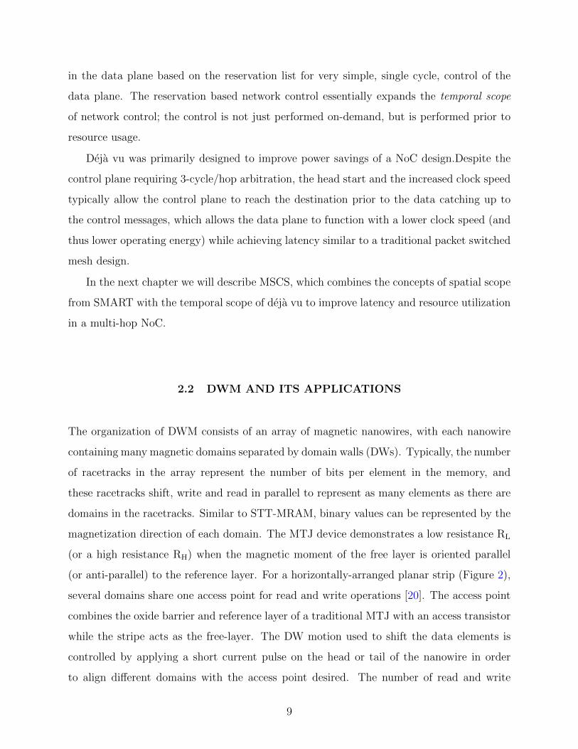
2.2 DWM AND ITS APPLICATIONS
The organization of DWM consists of an array of magnetic nanowires, with each nanowire
containing many magnetic domains separated by domain walls (DWs). Typically, the number
of racetracks in the array represent the number of bits per element in the memory, and
these racetracks shift, write and read in parallel to represent as many elements as there are
domains in the racetracks. Similar to STT-MRAM, binary values can be represented by the
magnetization direction of each domain. The MTJ device demonstrates a low resistance RL
(or a high resistance RH) when the magnetic moment of the free layer is oriented parallel
(or anti-parallel) to the reference layer. For a horizontally-arranged planar strip (Figure 2),
several domains share one access point for read and write operations [20]. The access point
combines the oxide barrier and reference layer of a traditional MTJ with an access transistor
while the stripe acts as the free-layer. The DW motion used to shift the data elements is
controlled by applying a short current pulse on the head or tail of the nanowire in order
to align different domains with the access point desired. The number of read and write
9

access points is correlated with the maximum density of the technology; one access point
per domain nearly eliminates the benefit of DWM density compared to STT-MRAM, while
having only one read/write access port causes limitations in performance. As a result,
the storage elements and access transistors do not directly correspond, and thus a random
access requires two steps to complete: Step 1–shift the target magnetic domain and align
it to an access transistor; Step 2–apply an appropriate voltage/current to read or write the
target bit. While a read operation in DWM for a domain under an access transistor is the
same as in STT-MRAM, the write can be a shift in an orthogonal dimension [1]. Thus,
the tradeoffs between DWM and STT-MRAM include reduced access power (due to fewer
access transistors per bit) and increased density at the cost of non-uniform access time and
potentially increased read times.
Various storage applications based on DWM have been demonstrated, including array
integration [21], lower level cache [22, 23], content addressable memory (CAM) design and
fabrication [24, 25], reconfigurable computing memory [26], and a GPU register file [27].
Further a fixed-length shift register, realized by perpendicular magnetic anisotropy (PMA)
technology, has been demonstrated [20, 28]. While these applications use DWM in random-
access applications, we examine DWM in the context of queue-oriented applications, which
has a unique set of constraints and concerns compared to random access. While there has
been a proposal to use DWM in FIFOs within a NoC [29], this proposal used the naive
circular control scheme we will discuss, and did not optimize Racetrack control for FIFOs.
Currently, substituting a considerable percentage of the SRAM within the network FIFOs
with STT-MRAM is a leading approach to reducing energy while maintaining the original
capacity [30]. In order to avoid the inefficiencies with the STT-MRAM writes, the proposed
scheme writes into SRAM first and then lazily migrates it to a reduced retention (i.e., a faster
lower write effort) STT-MRAM [31, 32] when possible. This method results in an energy
savings of 16% compared to existing FIFO buffers. In contrast, our designs with DWM NoC
FIFOS replace the SRAM entirely with very little (e.g., a single-flit) or no SRAM buffering
required. We describe our DWM-based variable length queue designs in chapter 4.
10

E-Out
Crossbar
S-Out W-Out N-Out C-Out
E-In
S-In
W-In
N-In
C-In
Rx
Tx
Full-swingLow-swing
Fig. 5: One-bit SMART Crossbar.
Input buffer
SMART Crossbar
5x5 xbar
E-OutE-In
S-In
W-In
N-In
C-In
S-Out
W-Out
N-Out
C-Out
Arbiters
SMART Router
Pipeline Buffer WriteSwitch
Allocation
SMART
Crossbar + Link
Bypass path
Fig. 6: SMART Router Microar-
chitecture and Pipeline.
12 13 14 15
8 9 10 11
4 5 6 7
0 1 2 3
1
1
1
1
1
1
1
1
1
1 1
1
1 4 7
7
7
7
11
4
7
7
Fig. 7: SMART NoC in action with four flows.
(The number next to each arrow indicates the
traversal time of that flow.)
SMART NoC with preset routes for four arbitrary flows. In
this example, the green and purple flows do not overlap with
any other flow, and thus traverse through a series of SMART
crossbars and links, incurring just a single-cycle delay from
the source NIC to the destination NIC, without entering any
of the intermediate routers. The red and blue flows, on the
other hand, overlap over the link between routers 9 and 10,
and thus need to be stopped at the routers before and after
this link to arbitrate for the shared crossbar ports7. The rest
of the traversal takes a single-cycle. It should be noted that
before the application is run, all the crossbar select lines are
preset such that they either always receive a flit from one of
the incoming links, or from a router buffer.
Since the routes are static, we adopt source routing and
encode the route in 2 bits for each router. At the source
router, the 2-bit corresponds to East, South, West and North
output ports, while at all other routers, the bits correspond to
Left, Right, Straight and Core. The direction Left, Right and
Straight are relative to the input port of the flit. In this work,
we avoid network deadlocks by enforcing a deadlock-free turn
model across the routes for all flows.8
Flow Control. In a conventional hop-by-hop traversal
model, a flit gets buffered at each hop. Thus, a router only
needs to keep track of the free VCs/buffers at its neighbors
before sending a flit out. Without loss of generality, we adopt
the virtual cut-through flow control to simplify the design. A
queue is maintained at each output port to track the available
free VCs at the downstream router connected to that output
port. A free VC is dequeued from this queue before a head
flit is sent out of the corresponding output port. Once a
VC becomes free at the downstream router, the router sends
a credit signal (VCid) back to the upstream router which
enqueues this VCid into the queue.
In the SMART NoC, a flit could traverse multiple hops
and get buffered, bringing up challenging flow control issues.
A router needs to keep track of free VCs at the endpoint
of an arbitrary SMART route, though it does not know the
SMART route till runtime. We solve this problem by using
7If flits from the red and blue flow arrive at router 9 at exactly the sametime, they will be sent out serially from the crossbar’s East output port.
8Deadlock can also be avoided by marking one of the VCs as an escapeVC [11] and enforcing a deadlock-free route within that. The exact deadlock-avoidance mechanism is orthogonal to this work.
a reverse credit mesh network, similar to the forward data
mesh network that delivers flits. The only overhead of the
credit mesh network is a [log(# VCs) + 1 (valid)]-bit SMART
crossbar added at each router. For example, if the number of
VCs is 2, the overhead of the credit network is 2-bit wide
crossbars. If a forward route is preset, the reverse credit route
is preset as well. A credit that traverses multiple hops does not
enter the intermediate routers and goes directly to the SMART
crossbar which redirects it along the correct direction.
For example, in Figure 7, for the blue flow, credits from
NIC3 are fowarded by preset credit crossbars at routers 3, 7
and 11 to router 10’s East output port in a single-cycle without
going into intermediate routers; credits from router 10’s West
input port are sent to router 9’s East output port and credits
from router 9’s West input port are sent to NIC8.
The beauty of this design is that the router does not need
to be aware of the reconfiguration and compute whether to
buffer/forward credits. Since the credits crossbars act as a
wrapper around the router, and are preset before the applica-
tion starts, the credits automatically get sent to the correct
routers/NICs. Thus, if a router receives a credit, it simply
enqueues the VCid into its free VC queue. This free VC queue
might actually be tracking the VCs at an input port of a router
multiple hops away, and not the neighbor, as explained above.
V. IMPLEMENTATION TOOL FLOW
To demonstrate the feasibility of the SMART NoC architec-
ture, we present a tool to build SMART NoCs. The tool takes
network configurations as input (e.g., the dimension of the
mesh, flit width, number of VCs and buffers), and generates
the RTL description as well as the layout of the SMART NoC
integrated with the proposed SMART link. We next describe
how each component is generated.
Voltage Lock Repeater. To integrate the VLRs into the de-
sign, we implement a SKILL script to take 1-bit Tx/Rx layout
and data width as input and place-and-route them regularly to
multi-bit Tx/Rx blocks. Figure 8 shows an example of a 32-bit
Tx block. We do not embed the VLRs in the crossbar as in [25]
because that leads to high area overhead. Also, we do not
use existing commercial place-and-route tools because these
tools are often designed for general circuit blocks and cannot
leverage the regularity property, adding unnecessary overhead.
In addition, the script also generates the timing liberty format
Figure 1: SMART traversal times for four concurrent, independent messages [4].
Shift
Shift
Write
Write
ReadNanowire
Domains
Domain Walls
Figure 2: The DWM design.
11

3.0 MSCS DESIGN
In this chapter, we describe the Multi-hop Segmented Circuit Switching router design. MSCS
leverages the pre-scheduling of resources in conjunction with global control and multi-hop
traversal. Similar to deja vu routing, the temporal scope of the network is expanded, as these
resources are pre-scheduled according to the arrival order of the packets, and do not require
timestamps. This feature combined with the per-dimension routing organization means that
network control is performed at most once or twice for a packet during its lifetime, reducing
temporal redundancy and network latency which would have otherwise occurred through
additional control and arbitration. In the following sections we describe the MSCS design
and details of its implementation.
3.1 DESIGN OVERVIEW
Multi-hop NoC routing brings the interconnect one step closer to true circuit switching. In
traditional circuit switching, the source router must send a circuit setup message to the
destination router in advance of a message to setup a circuit. The intermediate routers
set and maintain their crossbar configuration according to the setup message. The control
overhead is paid once during circuit setup time; when a circuit is established, data packets
can traverse the circuit without the impediment of local network control, and no buffer is
required for data packets because there is no possible contention. [33]
However, there is a significant drawback with circuit switching: the circuit setup over-
head. The source router sends a circuit setup message to the destination router, and has
to wait for an acknowledgment from the destination router before sending the data packet.
12

The acknowledgment wait time from the destination router varies depending on the type
of network used and the contention experienced by the setup message. The requisitioned
resources along the path of a circuit cannot be used by any other circuit during a setup
request, creating potential for idle resources, latency degradation, and throughput loss.
MSCS enhances circuit switching with a circuit reservation mechanism. As resources of a
router (i.e. crossbar connections and data links) are exclusively allocated in circuit switching
to a single circuit request, an allocated resource cannot be reassigned to other circuits until
circuit teardown. Thus, circuit switching handles contention through single assignment of a
resource. In contrast, MSCS reserves that resource for future use instead of acquiring the
resource directly. When the reservation becomes available, which could happen immediately
in low contention scenarios, the message is sent. Therefore circuit reservation is analogous
to a circuit setup request in traditional circuit switching.
To realize these reservations in MSCS, each router contains a FIFO reservation queue for
each network direction. A reservation is popped from the queue when the circuit associated
with that reservation is finished sending data, which is similar to circuit teardown in baseline
circuit switching. By doing this, resources are granted to circuits in FIFO order, and circuits
are also established and torn down in the same order.
MSCS also requires a multi-hop (broadcast) network as the circuit request network.
This is needed for two reasons: First, the data network is capable of multi-hop traversal,
and thus the circuit request network must match the speed of data network. Second, circuit
reservation orders must be globally consistent. Broadcasting ensures that a reservation‘s
en-queue time (and order) is the same for all routers along the route. If two reservations are
broadcasted at the same time, then a global priority scheme, or arbitration, is utilized by
the routers to determine reservation queuing order.
To increase throughput, MSCS adds a buffer to every input port of the data network
to allow messages to traverse available circuit segments and buffer data downstream along
the message route where earlier reservations are still being satisfied. In contrast to circuit
switching, this data buffer adds resource overhead and necessitates buffer flow control but
does not require a fully established circuit to send a data packet. This removes the acknowl-
edgment requirement of the complete circuit setup and decreases the circuit control delay
13

Latch
0
1
Packet Buffer
0
1
0
1
0
1
IncomingFlits
Circuit Path
Buffer Bypass
ToCrossbar
Figure 3: The MSCS input port.
compared to circuit switching, even under zero network load. In the next several sections
we describe in detail the implementation of data path, flow control, and circuit reservation
network to realize MSCS.
3.2 FLOW CONTROL
The one data buffer per input port in MSCS necessitates buffer flow control. Fortunately,
the flow control mechanism of MSCS does not delay the data path, and, consequently, it
does not incur performance degradation. We employ a similar multi-hop traversal technique
proposed by SMART [4], since the data path of MSCS and SMART are similar.
Multi-hop traversal replaces the traditional clocked wire repeaters with asynchronous
repeaters which boost flits and allow fast multi-mm propagation1. At the conclusion of a
multi-hop traversal, a flit must be latched at the ending router’s input port (see Figure 3).
Both flit traversal and latching are done in a single cycle. In the cycle following a circuit
segment traversal the flit is written into the data buffer if the next circuit segment is not
available or if the flit has reached its destination router. If the next segment is available the
flit can be reinjected from the latch directly. Note, a flit may not continue along the route
1SMART links are reported to traverse 8 mm in a 2GHz cycle [4].
14
if either the current router output port is serving another reservation or if the next buffer
downstream does not have sufficient input buffer space to hold the flit.
The latter case is required to ensure that if the available circuit segment ends with the
next router it can be appropriately buffered. To accomplish this, MSCS uses on/off flow
control. There is one buffer on/off line from each of the neighboring routers. If the line
is on, enough buffer space is available and the crossbar connection and input buffering is
determined solely by circuit reservation. Otherwise, if the line is off, the input port must
buffer the incoming flit and not make any crossbar connection for that direction. To avoid
flow control delays, the buffer availability of the subsequent cycle can be determined in the
current cycle. For example, the router can report the reservation will be consumed and allow
the next reservation to send in the following cycle if it is handling the tail flit of the currently
reserved connection.
3.3 CIRCUIT RESERVATION REQUEST NETWORK
To reduce complexity, we restrict the routing algorithm to X-Y routing (dimension-order
routing) with the standard 2D mesh. Thus, the path of a packet has at most one turn. The
reservation request procedure is naturally divided into two broadcasts, a request broadcast
for the X dimension and another for the Y dimension. For each row or column of the 2D
mesh network, the circuit request network is the same as 1D mesh.
Circuit reservations in one dimension: A circuit request network consists of three
buses—an arbitration bus, a request bus, and a flow-control bus. The size for these buses
per row/column are N bits, log(N) bits, and N bits, respectively, where N is the size of a row
in an N×N mesh. The source router of a packet uses the request bus to broadcast its circuit
request, while the arbitration bus handles potential conflicts among multiple source routers.
During the arbitration stage, source routers assert their own bit lines of the arbitration bus,
and all the routers use round robin arbitration to chose among the relevant candidate source
routers. To broadcast a circuit request, the winner puts the row/column number of the
destination node on the request bus. All nodes have the winner source node‘s row/column
15

number after arbitration, and those nodes also have the destination node’s row/column
number after the broadcast.
To deal with potential reservation buffer overflow, a router asserts its bit line on the flow-
control bus if its reservation buffer is full. A source node will not make a circuit reservation
if the circuit has a full router on its path, since the reservation will fail.
Circuit reservations in multiple dimensions: When introducing additional dimensions,
for X-Y routing, a packet traverses the entire X dimension first followed by the Y. Each
dimension can utilize the circuit reservation from the single dimension case. We assume
the packet must re-arbitrate when changing dimension. This could potentially hinder traffic
in the first dimension along that route, significantly reducing throughput. We solve this
problem by removing the waiting packet for the new dimension to a data buffer separated
from the original dimension. We call this a relay buffer as it relays a packet from one
dimension to the next.
3.4 DATA PATH
To build a MSCS 2D mesh crossbar, it is necessary to change the crossbar design of the
regular mesh. Figure 4 shows the modified crossbar design. The router has two small
crossbars (3x4 and 4x3) instead of a single large 5x5 crossbar. In terms of energy efficiency
and area, the two smaller crossbars actually use less power and area than a 5x5 crossbar.
In X-Y routing, a packet turning from the X to Y dimension is buffered at the relay buffer
and no longer blocks the X dimension. At this point, the packet makes a circuit reservation
for the Y dimension from the relay buffer. The relay buffer serves as a single point of entry of
the Y dimension for incoming packets from either the east or west direction. Arbitration is
needed to resolve potential contention between central-in (messages that only require the Y
dimension) and the relay buffer. The arbitration latency can be amortized by using natural
parallelism that exists in the circuit request pipeline, so it does not require an additional
pipeline stage.
16

Further, a control register is required between the data path (crossbar and input port)
and the circuit control unit. The control register is a latch that holds the setup signal from
the control unit to the crossbar and the input port. The control register is set by the control
unit one cycle ahead.
There are only two pipeline stages for MSCS: reservation and traversal. When the
reservation entry is generated, it is given to the circuit setup logic to set the control logic
in parallel to writing the reservation queue. At the beginning of the next cycle, the control
register is already set, and the data path can begin immediately if the resources are available.
Furthermore, we add a second read port for the reservation queue to read the top two
reservations in order to calculate the next circuit’s configuration prior to the current circuit’s
teardown and establish it immediately in the next cycle. An auxiliary control register is
required to store this calculated configuration.
The circuit request latency overhead with no contention is at most two cycles for a packet
and only one cycle for requesting a circuit that travels in only one dimension. For a data
packet with multiple flits, the overhead is amortized. For circuits that cannot be established
for more than one cycle due to contention, the circuit establishment overhead is entirely
hidden as the packet must already wait for the contention to clear to use the resource.
To illustrate MSCS NoC traversal, an example of four concurrent messages with one-flit
packets is shown in Figure 5. This example assumes all four packets enter the traversal stage
at time 1. The green flow’s reservation had precedence over the red flow, so the red flow
must buffer at the east ingress of router 14. In cycle 2, the red flow can traverse to the
east ingress of router 13, as the green flow is now holding the relay buffer. Simultaneously,
relay arbitration occurs for the green flow. In the cycle that the green flow leaves the relay
queue (cycle 3), the red flow performs switch traversal and buffer write into the relay queue.
Following this, the red flow performs arbitration (cycle 4), and finally, in cycle 5 it can
complete switch and link traversal to its destination.
17

Central_in Relay
East_out
South_in
East_in
West_out
4X3
3X4
Central_out
North_out
South_out
North_in
West_in
Figure 4: The relay crossbar adjustments for MSCS.
3.5 COMPARING MSCS WITH SMART
Both SMART and MSCS use global control and multi-hop traversal, but MSCS uses circuit
switching and reservations, while SMART uses on-demand network control. SMART per-
forms arbitrations each cycle on a per packet basis, which incurs latency due to the repeated
per packet controls. MSCS’s FIFO reservation queues handle and maintain the global and
local arbitration, so that circuits can be established when the resources become available
without performing latency inducing arbitration at each step.
To illustrate this situation, in both SMART and MSCS, a packet can traverse a circuit
segment and be stopped prematurely and short of its intended destination due to downstream
buffer occupancy. When the downstream buffer becomes available, the packet can resume
its traversal. For MSCS, resuming traversal happens during the same cycle that buffer space
becomes available and requires no control delay due to the circuit reservation. For SMART,
there is a minimum additional two cycle startup latency for resuming packet traversal, since
SMART needs to perform local and global arbitration each time before sending a packet.
18

0 1 2 3
4 5 6 7
8 9 10 11
12 13 14 15
1
1
1
1
1
relay
1
1 1 1
3
3
3
relay
3
3
3
3 11
1
2
3
5
5
5
Figure 5: MSCS traversal times for four concurrent, independent messages, with one relay
queue. With two relay queues, the red flow could enter a relay queue in router 13 at cycle 2.
19

4.0 DESIGNING QUEUES WITH DWM
At first glance, DWM appears naturally suited to implement queue structures. In fact, DWM
can naturally implement stacks and fixed length queues. However, implementing efficient
variable length FIFO queues, as required in network applications, is non-trivial. In this
chapter, we describe our methodology for building variable length queues from DWM, and
develop quantitative descriptions of these proposed queue approaches based on the physical
parameters of the DWM.
4.1 DWM PHYSICAL DESIGN
Traditional FIFO architectures utilize head and tail counters to implement a circular buffer,
where the head and tail pointers (tracking the next write and read locations, respectively)
can wrap around the array. While this configuration naturally lends itself to array-based
memory technologies (e.g., SRAM), it does not naturally extend to DWM. DWM has a
non-uniform access time due to the shifting required for alignment with an access port. In
Figure 6, we present three DWM-based queues where the queue is implemented as a group
of N simultaneously shifted Racetracks and N is the number of bits in a flit. Thus, each
“domain” represents storage for a flit. Moving forward, we describe operations for a buffer
assuming each operation will be completed simultaneously for all N Racetracks in parallel.
Figure 6 (a) shows the circular buffer (CB) implementation using DWM. We start with
a single read/write port in the center. A FIFO write shifts the Racetrack (if necessary) to
align the tail domain with the access point (step 1) and then to write (step 2) using the
orthogonal shift-write. For reading, the head domain is aligned with an access point and
20

(a) DWMvariable queue, circular
(b) DWMvariable queue, linear
R/W
Head
Tail
Head
Tail
Grow
s
R RR R
R R R R
Overhead Overhead
W
(c) DWMvariable queue, dual He
ad
Tail
Grow
s
R RW
Head
Tail
Grow
s
R RW
Figure 6: FIFO queue structure with DWM. (a) traditional circular buffer (CB). (b) shift-
register approach (LB) (c) dual shift-register approach (Dual).
then read by applying a current. Immediately, several undesirable characteristics become
apparent. First, to align the leftmost or rightmost domain with the access point requires a
nanowire that is essentially twice as long as the useful storage in the device [regions indicated
by “overhead” in (a)]. This makes the nanowire larger and requires more shifting. Also, it
may be necessary to shift the full logical length of the Racetrack between subsequent writes.
Further, most FIFOs are assumed to be able to read and write simultaneously, which is not
possible in most configurations.
To address these inefficiencies we consider three approaches, a linear buffer (LB) concept
[Figure 6 (b)] that shifts data through the Racetrack like a shift-chain, an increase in the
number of access points, and the introduction of temporary SRAM storage to buffer reads
or writes to move them off the critical path.
The Linear Buffer: We propose a new hardware architecture, referred to as Linear Buffer
(LB), to attempt to mitigate the inefficiencies with the circular buffer approach. LB config-
urations write at one end of the queue, and then shift the data into the queue in analogous
fashion to a shift register, keeping the data contiguous. LB saves space over CB because it
does not require any additional overhead; it can read and write until it reaches maximum
capacity without shifting valid data out of the Racetrack.
21

Increasing the Number of Access Points: It has been demonstrated that a multiple read
port Racetrack does not detract significantly from the density achievable by the nanowire
because of the small relative size of read ports [22, 34]. Thus, it is reasonable to introduce
additional read access points to all physical schemes to increase performance at the cost
of some additional static power. One possible configuration for each of CB and LB using
additional read ports is displayed in Figure 6 with dashed lines. Note that having a read
port for every domain would be physically impractical, since it would result in the DWM
losing much of its physical size advantage over STT-MRAM.
Introduction of SRAM Storage: All physical DWM queues can be augmented with an
additional SRAM or STT-MRAM buffer to attempt to improve their performance. However,
while the buffer improves performance in most cases, it also comes with a significant negative
tradeoff in power. This approach will be considered in greater detail in the full-system
simulation in chapter 7.
While LB significantly reduces write delays compared to CB, consecutive reads in ei-
ther scheme continue to introduce additional read latency even when including a single-flit
SRAM head buffer and prioritizing reads due to the longer operation time compared to shift-
ing/writing. In order to mitigate this concern, we propose using Dual Linear Buffers (Dual).
Each of the nanowires is half the length, but also has half the read access points of the LB
[Figure 6 (c)]. The two-Racetrack structure allows alternating reads and writes essentially
creating the illusion of a dual port. For example, one Racetrack can shift to prepare for an
access while the other is accessed.
4.2 TERMINOLOGY AND ASSUMPTIONS
When discussing the physical topology of the DWM queue it is helpful to define some ter-
minology and parameters used in organizing the queue.
The read offset F is the space between the write head and the first read head. In order
to simplify the control and design logic, the distance between all read heads is enforced
to be uniform, and is denoted as by a read separation parameter N . In addition, the
22

maximum gap G, is defined as the larger of either the read separation N or the read offset
F , G = max(N,F ). The length of the Racetrack denoted as L and is equivalent to logical
queue capacity. Finally, as demonstrated in several other macro-cell DWM systems [1, 22],
we assume that each Racetrack only has one write port, in part to maintain an area advantage
of DWM over SRAM and STT-MRAM.
To consider the performance of different designs a second set of terms is required including
the shift speed S, the reading time R, the writing speed W , and the chosen cycle time
C of operation. Since the write operation can be completed as a shift in an orthogonal
dimension [1], from this point on we will assume that the write speed is equivalent to the
shift speed. Currently, reading for domain-wall memory is the latency bottleneck for the
technology [35], so in most of our control designs the C will be chosen to permit R along
with the delay of the peripheral circuitry.
Finally, several other assumptions were made to keep the control logic manageable. First,
we assume the data in the queue must remain in order. Second, the data must be maintained
without gaps or empty domains between valid data. For CB, this implies that if the head
points to position H the data will be written in position (H+ 1) mod L. For LB, this means
that the data is always written into position 0, and only when the most recently written data
is adjacent at position 1. For Dual, writes alternate between each half queue, but otherwise
follow the same restrictions as LB. Also, we assume that reads and writes are permitted at
any cycle where the queue is not empty or full, respectively.
4.3 SHIFTING CONTROL AND POLICIES
In traditional SRAM queues with uniform random access, read and write ports can be
implemented independently. However, queues composed of DWM may have to delay accesses
because ports are busy due to misalignment with the requested data or storage location. As a
result, the queues must also have a read-pending and write-pending signal, which is asserted
on a read or write that cannot be completed because the port is busy. This signal forces the
queue to focus on the pending access. For example, in the case of a pending write, the queue
23

would shift to align with the write head (having its most recently written data in position
1) and wait until the write occurs before allowing another operation. In this case, the queue
would only service reads if it did not interfere with being available to write. A similar case
can be envisioned for a pending read.
For each configuration (LB, CB, Dual), after performing a write, a read, or a no-op, it is
possible that there may be enough time left in a cycle to also perform additional shifting to
put the queue in better position to service future accesses. The decision on what proactive
shifting to complete is split into two main methods of control:
(1) stay-in-place: With stay-in-place, the queue will remain in its current position,
and not attempt to proactively shift to any position to anticipate a read or write. Instead,
the stay-in-place scheme only shifts when either the write-pending or read-pending signal is
asserted, or the queue is in a position where it can service a read or a write in the current
cycle, and as part of that service it must shift. This strategy is common in many domain-wall
memory designs for random-access applications.
(2) shift-to-home: Shift-to-home policies in general attempt to use spare cycles and
shifting opportunities to align with a predetermined access point, known as its ’home’, when-
ever the queue does not have a read-pending or write-pending signal active. For a CB,
there are two possible homes: the location at which the tail is aligned with the write head
(shift-to-write), and the position where the head is aligned with the closest read head (shift-
to-read). For the LB (and the underlying queues that form Dual), there are three possible
homes: (shift-to-read-forward) aligning the head pointer with the closest read head to the
right, (shift-to-read-back) aligning with the closest read head to its left (assuming sufficient
space/padding to prevent data loss), or (shift-to-write) aligning the tail pointer to the write
head.
4.4 IMPACTS OF SHIFT SPEED
This section establishes the correlation between the shifting speed of a Racetrack and its
observed latency. Since the latency is data dependent, we focus on the calculation of the
24

maximum number of useful shifts in a cycle: the shift speed above which latency will not
improve for any possible pattern of read and write accesses. For instances of CB, LB, and
Dual control where the cycle time is based on read latency, the following methods can be
used to calculate this quantity. For stay-in-place or shift-to-write schemes, the maximum
number of shifts it would take for a queue with one element to shift before being able to
write plus the distance to shift to home would yield the shifts-per-cycle which provides the
maximum performance. For shift-to-read schemes, determining similar expressions becomes
a maximization problem dependent on the number of elements in the queue and the location
of the read heads.
An example of the maximum useful shifts in a cycle for a LB with a shift-to-read-back
is shown in Figure 7 where blue indicates valid data and gray indicates unused space. The
worst case start for an LB queue is that the tail is G positions away from being aligned with
the write head, where G = 2 in Figure 7 (a). The reason for this worst-case distance from
aligning with the write head is that shift-to-read-back will always shift left to align with the
read head if it is possible to do so while not blocking the write port. When a write arrives,
the Racetrack now must shift G positions to align its tail with the write access point, shown
in black in Figure 7 (b) and takes one additional shift to complete the write (as part of
the shift-based write). Following this, the queue attempts to realign with the closest access
point. Since the Racetrack cannot shift left because there is no padding to the left of the
tail, it shifts right two positions to align with the next read head requiring an additional
G shifts. Thus, the total shifts for this operation is 2G + 1 (or five as shown in Figure
7). The maximum useful shifts per cycle expressions can similarly be determined for other
architectures and policies, and the results are reported in Table 1.
4.5 IMPACT OF READ TO SHIFT TIME RATIO AND POST-READ
SHIFTS
When a Racetrack can perform x number of shifts in addition to performing a read within a
cycle, then we say that the queue has x post-read shifts. One solution to reduce the latency
25

for any Racetrack queue is to increase post-read shifts in a cycle; however, at a certain point,
there will be a cycle time Cmax (defined as the maximum useful cycle time) which will have
no latency degradation for any combination of inputs. Equivalently, this means that Cmax
is the minimum cycle time at which the queue is guaranteed to be able to both read and
write every cycle. In this section, we calculate the maximum useful cycle times for each
combination of shift policy and Racetrack hardware.
There are three primary queue positions which contribute to the calculation of the max-
imum useful cycle time. The first originates from the time it takes for LB or Dual with
two elements at the far end of the queue to both read and write in that cycle (represented
by α and αh, respectively in Table 2). One example of this situation is shown in Figure 8
(a), which contributes the time for L − 2 shifts (L − 3 actual shifts and one shift delay to
write) and one read delay R. For L = 10 this results in α = 8S +R. The shift-to-write and
shift-to-read-back schemes do not include this term, because they are guaranteed to have
a maximum difference between the tail data and the write head of at most G. CB has a
slightly different term, LS+R, because it is dependent on the situation where the write head
must shift the logical length of the Racetrack and conduct a read and a write sequentially
within a cycle.
The second contributing factor occurs when the queue must shift the maximum gap, G,
in order to read and write in a cycle (represented by β in Table 2). An example of this is
demonstrated in Figure 8 (b) where G = 5 requiring G shifts, one shift delay to write, and
one read delay R, totaling β = 6S+R. The final scenario occurs when the data is located in
the middle of the gap and cannot be read on the way to write (represented as γ in Table 2).
This scenario is demonstrated for LB in Figure 8 (c). In this examples where G = 5, the
queue shifts right two locations, reads, shifts left four locations and writes, contributing
γ = 7S +R.
The home policy dictates which of these conditions contribute to the maximum cycle
time. It turns out that for LB, shift-to-read-back and shift-to-write are only dependent on
conditions two and three (β, γ), while the others also depend on α. The maximum useful
cycle time for a control scheme is the maximum of the conditions which apply to that scheme.
Therefore, in the example in Figure 8, LB stay and LB shift-to-read-forward would have a
26

max cycle time of 8S +R, while LB shift-to-write and shift-to-read-back would have a max
useful cycle time of 7S+R. The maximum cycle time follows this logic for the other schemes
as well, and the summary of the times can be seen in Table 2.
4.6 IMPACTS OF SIZING CYCLE TO READ LATENCY
Since the read latency is the limiting performance characteristic (highest latency operation)
in DWM, as mentioned previously, it is natural to choose the cycle time as close to the read
time as possible. However, if there is not enough time to both read and shift in a cycle, then
there is no possible configuration of writing speeds, shifting speeds, and distance between
read heads for a single Racetrack which can always service both a read and a write request in
a cycle. This limitation arises from two origins: only having one write head per Racetrack,
and not being able to shift the Racetrack in the same cycle as it is read. This can be easily
proved by contradiction by considering a situation were the Racetrack begins with at least
1 element and then must service both a read and a write in two consecutive cycles.
4.7 DWM STATE MACHINE DESIGN
The algorithms presented in the previous few sections are not designed for optimized hard-
ware implementation. Therefore, in this section we present a hardware optimized methods
to implement control focusing on the specific example of two shifts-per-cycle, a read offset
of zero, a read separation of one, and no post-read shifts in a cycle. All other parameter
combinations can be similarly expanded into hardware control implementations.
The CB scheme uses traditional head/tail pointers to determine shift locations, the LB
scheme requires a finite state machine (FSM) for control as shown in Figure 9. There are
four states possible for the buffer (see Figure 10): RW-Aligned, where the queue head is
aligned with a read access point and the tail pointer is aligned with the write access point,
R-Aligned where the queue head is aligned with a read access point but the tail pointer is
27

not, W-Aligned where the tail pointer is aligned with the write access port but the head
is not aligned with a read access point, and Unaligned where neither the head nor tail
is aligned with an access point. This FSM can easily be expanded for a larger gap (more
domains) between read access points through additional “unaligned” states.
There are four possible permutations of operations for each state: buffer read, write,
both read and write, or idle. In the RW-Aligned state all requests can be handled directly.
On a read, the head is read and the state moves to W-Aligned. On a write, the FSM writes
and shifts right the Racetrack and the state also moves to W-Aligned. For both a read
and write, the FSM simultaneously writes and reads and moves to the unaligned state. In
unaligned, if idle (or a R occurs) the Racetrack buffer shifts right and moves to the RW-
Aligned state in the next cycle (read still pending). If a write (or read and write) occurs,
the queue shifts right and writes in a cycle moving to R-Aligned (read still pending). The
other states proceed in a similar way with certain options able to be serviced directly, and
those in parenthesis requiring multiple cycles to complete. We track the current active read
head using a simple shift register of the same length as the number of flits that shifts in
the same direction as data of the Racetrack queue. This simple shift register could also
be implemented using a DWM, although during our analysis of the peripheral circuitry we
assume it is implemented in traditional CMOS. These operations (noted by << and >>) as
well as other state transitions not explicitly described are enumerated in Figure 9.
Dual and LB have very similar FSM structure. For Dual, we include two additional
control bits, “Read Owner” and “Write Owner” to manage which Racetrack is accessed in
each cycle. For each access, the owner bit is flipped. In the example from Figure 11, the
queue holds five flits, it is in the RW-Aligned state, the next read comes from queue ‘1’ and
the next write goes to queue ‘0’, both of which may proceed in parallel. The read head is
indexed by the “Read Owner” and a single bit RC (shown in the Figure as the R indices).
Overall Dual has a similar control overhead to LB.
28

4.8 RACETRACK OVERHEADS
The overhead of the CB scheme includes read and write pointers (lg(N) bits each), a stored
current offset value for Racetrack (lg(N) bits), comparitor, increment and decrement cir-
cuitry, N−1 extra domains to prevent loss of data when shifting to the ends of the Racetrack
[see Figure 6 (a)], and the stored locations of the read and read/write access points. Note, it
does not require the one-hot head and tail pointer storage because it does not use these bits
to energize a word-line as in traditional array-based storage. If the CB scheme is augmented
with an SRAM buffer, the additional overhead includes a one-flit buffer plus an additional
one valid bit per Racetrack.
For LB only N domains are required as compared to the 2N − 1 domains per Racetrack
for CB. The overhead for this scheme includes two bits of storage to represent four states,
and the same number of bits as the number of read heads (1 hot, in a shift register) for
the currently used read head plus the same overhead for an additional SRAM buffer as CB.
Similarly, in the Dual scheme, N domains are required per buffer (N2
for each Racetrack).
The overhead for the Dual scheme includes two bits per Racetrack to represent the four
states, one bit per buffer to represent the valid read head1 and two bits per buffer to indicate
which Racetrack is controlling the buffer reads and writes (i.e., the read and write owner
of the buffer, respectively, in Figure 11). The Dual scheme does add additional peripheral
circuitry to write to and shift two half length Racetracks, which is accounted for in the
energy calculations presented in chapter 7.
1This is a special case for Dual where each Racetrack has two read heads specified by that valid readhead bit, otherwise each Racetrack would require an RC Shift Register circuit as in the LB control.
29

Table 1: Maximum useful shifts per cycle. Assumes queue cannot shift and read in same
cycle and no padding linear/dual queues.
Circular Stay-in-Place Shift-to-Write Shift-to-Read
Shifts, Align with Write L-1 L-1 L-1*
Home Shifts 0 1 G+1*
Total(+sb-write) L L+1 L+G+1*
Linear Stay-in-Place Shift-to-Write Forward Back
Shifts, Align with Write L-2 G L-2* G
Home Shifts 0 1 G* G
Total (+sb-write) L-1 G+2 L-1+G* 2G+1
Dual Stay-in-Place Shift-to-Write Forward Back
Shifts, Align with Write L2− 2 G L
2− 2* G
Home Shifts 0 1 G* G
Total (+sb-write) L2− 1 G+2 L
2− 1 +G* 2G+1
* Indicates worst case but not the general case. Certain configurations of read heads
may result in this number being reduced, but the order (e.g., linear with L + G)
remains the same.
W R R R
W
W R R R
R R R(b)
(a)
(c)
Figure 7: Linear Buffer shift-to-read-back maximum useful shifts/cycle writing example, 0
post-read shifts and 0 padding.
30

Table 2: Maximum useful cycle times (not including peripheral circuitry delay)
Circular Stay-in-Place Write Read
max(L ∗ S +R, γ)
Linear Stay-in-Place Write Read Fwd Read Back
max(α, β, γ) max(β, γ) max(α, β, γ) max(β, γ)
Dual Stay-in-Place Write Read Fwd Read Back
max(αh, β, γ) max(β, γ) max(αh, β, γ) max(β, γ)
α : (L− 2) ∗ S +R β : (1 +G) ∗ S +R
αh : (L2− 2) ∗ S +R γ : (3∗G
2− (G− 1)%2) ∗ S +R
W R R
W
(a)
W R R
R R
(b)
(c)
Figure 8: Maximum useful cycle examples for LB.
31

RW-‐Aligned
R-‐Aligned
W-‐Aligned
Unaligned
W R/[<<RC]
W/[>>RC]
Idle (R) R+W (R)
W R
W/[>>RC]
RC Shift Register 0 0 1 0 R2 R1 R0 R3
Figure 9: Linear buffer FSM. R=read, (R)=read align RT, W=write, R+W=read and write,
Idle=neither read nor write. [<<RC] and [>>RC] also shift the read port left and right,
respectively, depicted in the RC Shift Register where the highlighted (‘1’) port is currently
selected.
RW-Aligned
W-Aligned
R-Aligned
Unaligned
W R2 R1 R0 R3
W R2 R1 R0 R3
W R2 R1 R0 R3
W R2 R1 R0 R3
Figure 10: Example queue conditions corresponding to LB FSM controller. Black regions
are valid flits.
32

Shift Right Shift Left
Shift Right Shift Left0
1
State RW--Aligned Write Owner: 1Read Owner: 0
R0,0 R0,1
R1,0 R1,1
W0
W1
Figure 11: Dual Racetrack design. The two Racetracks together comprise one NoC buffer.
33

5.0 MSCS RESULTS
To evaluate the impact of MSCS, we constructed a cycle accurate router implementation
of MSCS using the gem5 [36] simulator. To assess the relative performance of MSCS, we
also implemented SMART faithfully based on the published manuscript [4] and use this
state-of-the-art design as our reference for comparison in our evaluation.
We performed both synthetic traffic network only simulations and full system simulations
on benchmark workloads. For synthetic traffic simulation, we use an 8× 8 as the underlying
topology. An 8×8 mesh is appropriate as it is used for existing commercial products such as
the Tilera 64 [37], and it is a common topology for performance evaluation in proposed NoC
research proposals. Each virtual channel buffer and relay buffer can hold eight flits. For full
system simulations, we used a set of selected benchmarks from parsec 2.1 [38] and splash-
2 [39] suites. The underlying system uses 64-core CMP with a standard shared last-level
cache system with the MESI coherence modeled by Ruby. Each core is a 3-issue out-of-order
X86 processing unit. The O3 CPU module in gem5 is used to model the core.
5.1 SYNTHETIC TRAFFIC ANALYSIS
Our synthetic traffic analysis used uniform random traffic. MSCS with a single buffer per
port and two and four relay buffers per network node was compared to SMART with two
and four virtual channel buffers per input port per node. This compares schemes with a 25%
and 50% reduction in virtual queues per node, respectively. The results of average network
latency for synthetic traffic with 5-flit packets can be observed in Figure 12. Over the scope
of the synthetic results until the start of saturation, the MSCS scheme with two relay buffers
34

per node results in a 50.5% latency reduction over SMART with two virtual queues per
input port, and continues to have lower latency with heavy traffic. MSCS with four relay
buffers per node produces a 16.7% reduction in network latency through the period depicted
in the graph (until the onset of saturation) over SMART with four virtual channel buffers.
However, past the onset of saturation, SMART with four virtual channel buffers outperforms
MSCS with four relay buffers (and half the virtual queues).
The average packet latency results of uniform random synthetic traffic with packets of
just one flit can be observed in Figure 13. Similar to the results for packets with five flits,
MSCS with two relay buffers consistently outperforms SMART with two virtual channels
per input port over all synthetic input traffic, with an average improvement of 36.6% before
saturation. However, SMART with four virtual channels per input port outperforms MSCS
with four relay buffers (half the number of virtual channels).
5.2 FULL SYSTEM EVALUATIONS
Average packet latency is shown for full system simulations under various workloads in
Figure 14. For this simulation, five flit packets were used, and SMART with one and two
virtual channels per port were compared against MSCS with one input buffer per port and
one relay buffer per node. On average, MSCS results in a 12.7% reduction from SMART
with one virtual channel per port, and a reduction of 1.4% from SMART with two virtual
channels per port, despite having 37.5% less buffer requirements per node.
35

1 flit
0.00
5.00
10.00
15.00
20.00
25.00
30.00
35.00
0.001 0.007 0.013 0.019 0.025 0.031 0.037 0.043 0.049 0.055 0.061 0.067
Ave
rage
Net
wo
rk L
aten
cy
Injection Rate
MCSC(2 relays) MSCS(4 relays) SMART 2VC SMART 4VC
0
5
10
15
20
25
30
35
0.001 0.021 0.041 0.061 0.081 0.101 0.121 0.141 0.161 0.181 0.201 0.221 0.241 0.261
Ave
rage
Net
wo
rk L
aten
cy
Injection Rate
MCSC(2 relays) MSCS(4 relays) SMART 2VC SMART 4VCFigure 12: Network latency for synthetic traffic, 5-flit packets.
1 flit
0.00
5.00
10.00
15.00
20.00
25.00
30.00
35.00
0.001 0.007 0.013 0.019 0.025 0.031 0.037 0.043 0.049 0.055 0.061 0.067
Ave
rage
Net
wo
rk L
aten
cy
Injection Rate
MCSC(2 relays) MSCS(4 relays) SMART 2VC SMART 4VC
0
5
10
15
20
25
30
35
0.001 0.021 0.041 0.061 0.081 0.101 0.121 0.141 0.161 0.181 0.201 0.221 0.241 0.261
Ave
rage
Net
wo
rk L
aten
cy
Injection Rate
MCSC(2 relays) MSCS(4 relays) SMART 2VC SMART 4VC
Figure 13: Network latency for synthetic traffic, 1-flit packets.
36

0
0.2
0.4
0.6
0.8
1
1.2
No
rmal
ized
Lat
ency
SMART-1VC SMART-2VC MSCS
Figure 14: Average network latency normalized to SMART with 1 virtual channel per input
port.
37

6.0 FIFO DESIGN SPACE ANALYSIS
In order to analyze the performance of DWM queues we began by evaluating the queues
independently based on different read and write traffic patterns. We simulated each queue
(e.g., CB, LB, Dual) for different parameters with different synthetically generated read and
write traffic patterns. For uniform random traffic, at each time step the chance of reading
was K, and the chance of writing was also K, as long as the queue was not empty/full,
respectively. Access latency is determined by the average delay from when the access request
arrives and when the access is completed. In chapter 4 we evaluated mathematically the
limits for useful range of parameters in DWM queue designs. In this chapter we evaluate
the practical sets of parameters from the design space using experiments with synthetic
workloads (results for the pattern ’shuffle’ are shown, but bitcomp and transpose had the
same trends). The resulting configurations are then evaluated using cycle-level analysis with
application workloads in the following chapter.
6.1 CONTROL SCHEMES
In this section we evaluate the effectiveness of the shifting policy, specifically stay-in-place,
shift-to-read, and shift-to-write, on overall performance of the CB and LB schemes.
6.1.1 Circular Buffer
To begin the analysis of the circular buffer, we first compare F = 0, N = 2 (read ports
adjacent to the central write port and a spacing of two between read heads) and F = 1,
38

N = 1 (read heads with an offset of one from the central write port and a spacing of one
between read heads). The physical layout of each of these cases are shown in Figure 15; as
shown, each configuration has four read heads.
Figure 16 demonstrates normalized read and write latencies, as well as total shifts for
CB under low (10%) traffic with four shifts-per-cycle and length L = 9. The traffic load is
defined as a Traffic = Read Write%cycle
representing the probability a write request and/or read
request be issued in that cycle. Shifts represent the total shifts the Racetrack made during
the simulation, Missed Reads are the total number of times the Racetrack received a read
request and could not service it in the same cycle, and Missed Writes represent the same
for writes. The Read Latency is the average amount of cycles a data element has to wait
before it can be written, and Write Latency is the same for writes. Since every element is
both written and read in a simulation, the Total Latency is defined as the sum of the read
and write latency.
In all cases, the number of shifts in the F = 1, N = 1 scheme is less than the F = 0,
N = 2 counterpart. In this comparison, the latency advantage for the F = 1, N = 1 is
18% and 9% for stay-in-place and shift-to-read, respectively, with a nominal 2% increase for
shift-to-write compared to F = 0, N = 2.
In Figure 17 we evaluate the impact of different traffic loads on queue latency for the
different shifting policies in CB. Each shifting scheme is evaluated with its best performing
read/write head layout (F = 0, N = 2 for shift-to-write, and F = 1, N = 1 otherwise). As
can be observed in the figure, CB with the shift-to-read control scheme has a later onset of
saturation, as well as a consistently reduced total latency before saturation. For example, at
the 10% Traffic point (shown in detail in Figure 16), the best CB stay-in-place scheme has a
76% higher latency than the best CB shift-to-read scheme. While the stay-in-place control
scheme shifts 21% less and has a simpler control design, the 76% latency degradation until
the onset of saturation makes it less attractive compared to the shift-to-read scheme. The
best shift-to-read control scheme also demonstrates better pre-saturation latency than the
shift-to-write scheme. At the same 10% point, the shift-to-write scheme has a 15% higher
latency, as well as 8% more shifts. Given this analysis we conclude that the best performing
39

control scheme for CB is shift-to-read with F = 1 and N = 1. From this point forward,
when we refer to CB, we are referring to this configuration of CB.
6.1.2 Linear Buffer
To evaluate the shifting performance for the LB, the best read head placement was more
obvious, F = 0, N = 1, for a length L = 8 queue with four read heads. In this configuration,
we show in Figure 18 when LB is observed for low (10%) synthetic traffic (e.g., the pre-
saturation region), the results follow a very similar trend to those for the CB. LB with the
shift-to-read-back control scheme consistently has lower access latency than all the other
schemes, shift-to-read-forward, shift-to-write, and stay-in-place for low traffic. Shift-to-read-
back also has the fewest shifts except stay-in-place. While shift-to-write tends to favor
writes and the two shift-to-read tends to favor reads, in a queue it is expected that each
queue element will be written and then read, so we focus on overall latency.
As demonstrated in Figure 19, all of the saturation regions are quite similar, but shift-
to-read-back saturates the latest, thus giving a slight edge in the post-saturation region.
Therefore with both CB and LB, we conclude that aligning with the read head (read-back
for LB) is the most efficient design choice. Because of these factors, from this point forward,
LB will refer to LB with the shift-to-read-back control scheme. Moreover, an analysis of the
Dual scheme mirrored the trends of the LB, thus, we also selected and will refer to Dual as
using a shift-to-read-back control scheme.
6.2 SHIFT SPEED
In this section, we examine the effect of altering the number of shifts per cycle on the
latency of LB, CB, and Dual queues. For CB queues, increasing the shifts-per-cycle can
have tremendous impacts in the pre-saturation region. As can be seen in Figure 20, as
the number of shifts-per-cycle increases, the pre-saturation region significantly increases.
Further, the latency in the pre-saturation region (in terms of cycles per access) improves as
40

well. For example, the latency is reduced by 5X at 10% traffic when increasing from one
to two shifts-per-cycle. For CB, Table 1 predicts a maximum useful shifts-per-cycle of at
least L − 1 (eight shifts-per-cycle in this L = 9 configuration), so it is reasonable that all
transitions from one to four shown in Figure 20 improve read and write latency.
LB queues also exhibit significant improvement in the pre-saturation region, with a
48% improvement in total latency at 10% traffic. Unlike CB, LB’s improvement in latency
plateaus after two shifts-per-cycle. While it was mathematically predicted that the maximum
performance would be found at three shifts-per-cycle, the traffic pattern necessary to take
advantage of that capability is rare.
In order to observe the changes with LB in greater detail, we also examined the change
in latency with LB queues with L = 8, N = 3, and F = 2, shown in Figure 21. Table 1 pre-
dicts the maximum useful shifts-per-cycle for this configuration is seven; however, the state
transition where having an extra shift from six to seven shifts-per-cycle is similarly rare.
Thus, six and seven shifts-per-cycle provide nearly identical results for this configuration of
LB. While at the maximum shifts-per-cycle the latency reaches its minimum, all increases
after four shifts-per-cycle are nominal (i.e., less than 0.1%). In our experimentation, similar
results were found for different read head configurations leading to the conclusion that even
though there is a mathematical limit of maximum shifts-per-cycle, LB configurations effec-
tively reaches its practical minimum latency at G+ 1 shifts-per-cycle, recalling that G is the
maximum read head separation (max(N,F )).
Dual queues, like LB queues for four read heads, have their latency improvement plateau
at two shifts-per-cycle, as can be seen in Figure 20. Even with one shift-per-cycle, it takes
high traffic (i.e., a read and/or write more than 80% of the cycles) for Dual to enter satu-
ration. At 10% traffic, two shifts-per-cycle has a 52% latency improvement over one shift-
per-cycle, and the percentage latency improvement provided by two shifts steadily increases
with the traffic.
When comparing CB, LB, and Dual queues in Figure 20, we observe that CB only
outperforms LB with one shift-per-cycle in the pre-saturation region once CB has four or
greater shifts-per-cycle. However, even in this case, LB with one shift-per-cycle has a later
onset of saturation. While LB queues consistently begin the onset of saturation around the
41

50% traffic mark (since they cannot read and write in consecutive cycles), Dual queues are
able to remain in the pre-saturation region until around 80% traffic. This difference primarily
arises from the parallel nature of Dual, where one queue can prepare for an operation while
the other is being accessed.
6.3 POST-READ SHIFTS
Another consideration of cycle latency is the combination of a read access with shifting within
a single cycle. Thus, we examine the effect of sizing the cycle to allow post-read shifts on the
access latency (in terms of cycles) of the LB, CB, and Dual queues. Figure 22 demonstrates
the effect of adding post-read shifts for a case with N = 1, F = 0, four shifts-per-cycle, and
L = 8. Table 2 predicts the minimum cycle time that can give performance without delay
is given by (1 +G) ∗ S +R resulting in 2S +R or two post-read shifts per cycle for LB and
Dual in this configuration. With N = 1, increasing the cycle time from R to R + S has a
significant positive impact on LB performance as well as significantly delaying the onset of
saturation from 50% to about 95% traffic, which is comparable to the onset of saturation
for Dual with zero post-read shifts. We quantified the latency improvement in Figure 23 for
10% traffic.
An interesting result is that CB, which typically falls far short of LB, with one post-read
shift actually outperforms LB with 0 post-read shifts. This lends credence to the importance
of including shifting and reading in the same cycle. However, CB, even with three post-read
shifts in a cycle still is outperformed by Dual and LB with 1 post-read shift-per-cycle. Of
course, increasing the cycle time results in an improvement in queue performance from a
queue state behavior perspective, but it comes at the obvious tradeoff of fewer cycles per
unit time, which may make the original cycle time more efficient for Dual, despite the queue
delays it incurs. However, if a particular queue realization changes the relationship of read
access latency to shift latency, this provides interesting insights on how to size a cycle.
42

6.4 READ HEADS
The number of read access points also provides an interesting tradeoff between static power,
area, and queue latency. Thus, we performed a design space exploration on the number of
read heads in the queue, and examine the effect it has on total latency. Figure 24 demon-
strates the effect of varying the number of read access points on latency for LB and Dual
schemes. CB schemes were also considered, but they again performed significantly worse
than LB in the pre-saturation region, and consistently had an earlier onset of saturation and
as a result are not displayed in detail in this section. For LB queues, as observed in section
6.2, all queues begin to saturate at or before 50% traffic, even with a read head in seven out
of eight positions. While the pre-saturation latency steadily decreases as the number of read
heads increases for LB, the 50% traffic limit is a fundamental limitation of not being able to
both read and write in consecutive cycles.
As previously mentioned, because Dual does not have the aforementioned limit, it can
break the 50% barrier with only two read access points (one per DWM). From Dual, the
most significant finding is that Dual with six read heads (three per DWM) results in no
additional latency and can guarantee a read+write every cycle. However, operating in this
configuration would eliminate the size advantage over STT-MRAM due to the port every cell,
and thus will not be seriously considered. Therefore, for practical purposes in our hardware
implementation, Dual, CB, and LB with four read heads is used, since they have lowest total
latency while still maintaining a significant area and power advantage over STT-MRAM. In
the next chapter we evaluate these configurations for application workloads in the context of
a full system simulation using Dual, CB, and LB DWM queues for network-on-chip buffers.
6.5 RESULTS OF DESIGN SPACE ANALYSIS
As discussed in sections 6.1 and 6.4, the shift-to-read and shift-to-read-back schemes consis-
tently outperform the other shifting policies, and therefore will be the schemes used during
the benchmark simulations in the next chapter. While having a read head every domain
43

of the queues would eliminate the advantage over STT-MRAM, previous work suggests it
would be feasible to place read heads every other element of the queue [22]. Doing so results
in 24% and 56% improvement for LB and Dual, respectively, at 10% traffic over having a
read head every third element. Because the standard FIFO queue size in a NoC is typically
eight, we will use four read heads for CB, LB, and Dual during the benchmark simulations.
In section 6.2, the latency of the queue saturates at two shifts-per-cycle for four read
heads with a queue size of eight; therefore, it makes sense to choose a shifting speed that
allows two shifts per cycle in the next section. Finally, in section 6.3, while adding post-read
shifts provided significant latency improvements, Dual already has very low latency with
four read heads and two shifts per cycle, and therefore increasing the cycle time would most
likely result in an overall decrease of throughput. We simulate benchmark traffic with zero
post-read shifts in the next chapter.
44

0 1 2 3 4 5 6 7 8W R RRR
0 1 2 3 4 5 6 7
W R R R
CBF=1, N=1
0 1 2 3 4 5 6 7 8W R RRR
CBF=0, N=2
R LBF=0, N=1
Figure 15: Physical layout of the different configurations used in the design space analysis
of the different shift control schemes.
76543210
Shifts Missed_Reads Missed_Writes Read_Latency Write_Latency Total Latency
CB Scheme Results, 10% R/W Traffic Per Cycle
CB_shift-to-write_F=0 CB_shift-to-write_F=1 CB_shift-to-read_F=0CB_shift-to-read_F=1 CB_stay_F=0 CB_stay_F=1
Figure 16: Normalized results for CB with 10% traffic, 4 shifts-per-cycle, 4 read heads, and
9 elements per queue.
45

0
5
10
15
20
25
10 15 20 25 30 35 40 45 50
Late
ncy
Read/Write % Per Cycle
Total Latency, CB Schemes
CB_shift-to-read CB_stay CB_shift-to-write
Figure 17: Latency results as traffic increases for CB at 4 shifts-per-cycle, 4 read heads, and
9 elements per queue.
01234567
Shifts Missed_Reads Missed_Writes Read_Latency Write_Latency Total Latency
LB Scheme Results, 10% R/W Per Cycle
LB_stay LB_shift-to-write LB_shift-to-read_fwd LB_shift-to-read_back
Figure 18: Synthetic traffic results for LB with low (10%) traffic at 2 shifts-per-cycle, 4 read
heads, and 8 elements per queue.
46

0
2
4
6
8
10
10 15 20 25 30 35 40 45 50
Late
ncy
Read/Write % Per Cycle
Total Latency, LB Schemes
Shift-to-read_back Shift-to-read_fwd Stay Shift-to-write
Figure 19: Latency results as traffic increases for different LB schemes at 2 shifts-per-cycle,
4 read heads, and 8 elements per queue.
0
10
20
30
10 20 30 40 50 60 70 80 90
Late
ncy
Read/Write % Per Cycle
Total Latency, Different SPC, 4 read heads
CB_1spc CB_2spc CB_3spc CB_4spcDual_1spc Dual_2+_spc LB_1spc LB_2+_spc
Figure 20: Latency as traffic increases with varying shifts-per-cycle for CB (L = 9) and LB
(L = 8), each with 4 read heads per queue.
47

0
5
10
15
10 15 20 25 30 35 40 45 50 55
Late
ncy
Read/Write % Per Cycle
Total Latency, Different Shifts-per-cycle, 2 Read Heads
LB_1spc LB_2spc LB_3spc LB_4spc LB_5spc LB_6+_spc
Figure 21: Latency as traffic increases for LB for various shifts-per-cycle, with 2 read heads
and 8 elements per queue.
05
10152025
10 20 30 40 50 60 70 80 90 100
Late
ncy
Read/Write % Per Cycle
Total Latency, Post-Read Shifts Per Cycle
CB_0postread CB_1postread CB_2postreadCB_3postread Dual_0/1 post_read Dual_2+/LB_2+ post readLB_0postread LB_1postread
Figure 22: Latency results as traffic increases with different post-read shift amounts, with 4
shifts-per-cycle, 4 read heads and 8 elements per queue.
48

Shifts Missed_Reads Missed_Writes Read_Latency
Dual1
0.5
0
1.5
2.5CB
2
LB_0postread
Dual_2postread
Total Latency
Post-Read Shifts, 10% R/W Per Cycle
CB_0postread
LB_1postread
CB_1postread
LB_2postread
CB_2postread
Dual_0postread
CB_3postread
Dual_1postread
LB
Write_Latency
Figure 23: Synthetic traffic results with low traffic, 4 shifts-per-cycle, 4 read heads, and 8
elements per queue for different amounts of post-read shifts in a cycle.
02468
101214
10 20 30 40 50 60 70 80 90
Late
ncy
Read/Write % Per Cycle
Total Latency, Different Numbers of Read Heads
Dual_2rh Dual_4rh Dual_6rh LB_1rh LB_2rh LB_3rh LB_4rh LB_7rh
Figure 24: Latency results as traffic increases over different read heads, with 2 shifts-per-cycle
and 8 elements per queue.
49

0.6 0.8 1
1.2 1.4 1.6 1.8 2
Blackscholes Canneal Dedup Ferret Fluidanimate Raytrace Vips X264 Average
Normalized
Laten
cy
SRAM/STT SRAM/STTHalf CB LB Dual CB+S LB+S Dual+S 4.9 11.6 5.2 3.2
Figure 25: Flit latency of Racetrack buffer schemes normalized to SRAM.
0.4
0.6
0.8
1
Blackscholes Canneal Dedup Ferret Fluidanimate Raytrace Vips X264 Average
Normalized
IPC
SRAM/STT SRAM/STTHalf CB LB Dual CB+S LB+S Dual+S
Figure 26: Full system performance (IPC) for different Racetrack buffer schemes normalized
to SRAM.
50

7.0 DWM BENCHMARK RESULTS
7.1 EXPERIMENTAL SETUP
Based on the best performing parameters in the queue simulator, we further tested DWM
buffers by implementing CB, LB, and Dual schemes to serve as virtual channel buffers in a
NoC using the cycle-accurate HORNET multicore simulator [40] to compute both average
flit latency and energy consumption. In addition, peripheral circuitry power calculations for
SRAM, STT-MRAM and different Racetrack FIFO schemes were analyzed using data from
[1, 2] and a modified version of NVSim [3]. Sniper [41] was used to generate workload traces
of the PARSEC benchmark suite [38] for the modified HORNET simulator. To estimate the
full system performance impact of the NoC, the HORNET generated latencies were then
used in a second full system simulation in Sniper to determine performance impact via IPC.
The tests were performed on a simulated 64-core network using one-queue-per-flow o1-
turn routing. In addition, each ingress port connecting a core to its neighbor has eight virtual
channels, each of which can store eight flits. CB, LB, and Dual were tested both with and
without a single flit SRAM storage to buffer the queue’s head flit. The full system simulated
out of order cores with multiple instruction issue per-cycle with private first level and a
distributed shared last level (L2) cache. When running the simulations, we assumed there was
no performance difference between SRAM and STT-MRAM as an optimistic implementation
of the leading STT-MRAM NoC buffer proposal [30]. Also, to compare the implementation
of the DWM technology with a more energy efficient, and for STT-MRAM area-equivalent
counter parts, both SRAM and STT-MRAM were also tested with half (4) the number of
queues per channel (referred to as SRAMHalf and STTHalf).
1Empty buffer accesses incur SRAM-only cost.
51

Table 3: Buffer power for different technologies using synthesized control logic, data from [1,
2] and calculated using a modified version of NVSim [3].
Static Power (µW) Dynamic Energy (pJ/bit)
mem. array & control read write shift
SRAM 22.60 0.27 0.12 —
STT 14.91 0.10 0.24 —
CB LB Dual
RT 7.76 7.91 9.61 0.10 0.062 0.062
RT+SRAM 10.23 10.39 11.40 0.371 0.361 0.062
To determine the control circuitry overhead from implementing LB and Dual, we created
an implementation of the FSM in 45nm standard cell ASIC hardware and compared it
with the traditional one-hot read and write points for traditional FIFOs. The RT control
had a nominal overhead increase in terms of area and energy (i.e., < 0.5µW) compared to
the traditional FIFO. The full energy parameters for virtual queues of 8 flits and 128 bits
per flit for Racetrack, SRAM, and STT-MRAM are reported in Table 3. The increase in
static power for LB and Dual respectively over CB results from small increases in control
circuitry and peripheral circuitry. Adding the single flit SRAM storage to the Racetrack
schemes increases both the static and dynamic power for reads and writes. The Racetrack
LB approach (7.9µW) requires about half the static power of an STT-MRAM array (14.9µW)
and one-third of an SRAM array (22.6µW). Dual still provides 36% and 57% static power
reduction over STT-MRAM and SRAM, respectively.
We assume a NoC clock speed of 1GHz which allows SRAM, STT-MRAM, and Racetrack
reads in a single cycle based on latency data from NVSIM and the literature [35]. STT-
MRAM writes are also optimistically assumed to be a single cycle [30] similar to SRAM,
while Racetrack shifts and writes take half a cycle allowing a Racetrack to conservatively
2Half schemes use 4 VCs.
52
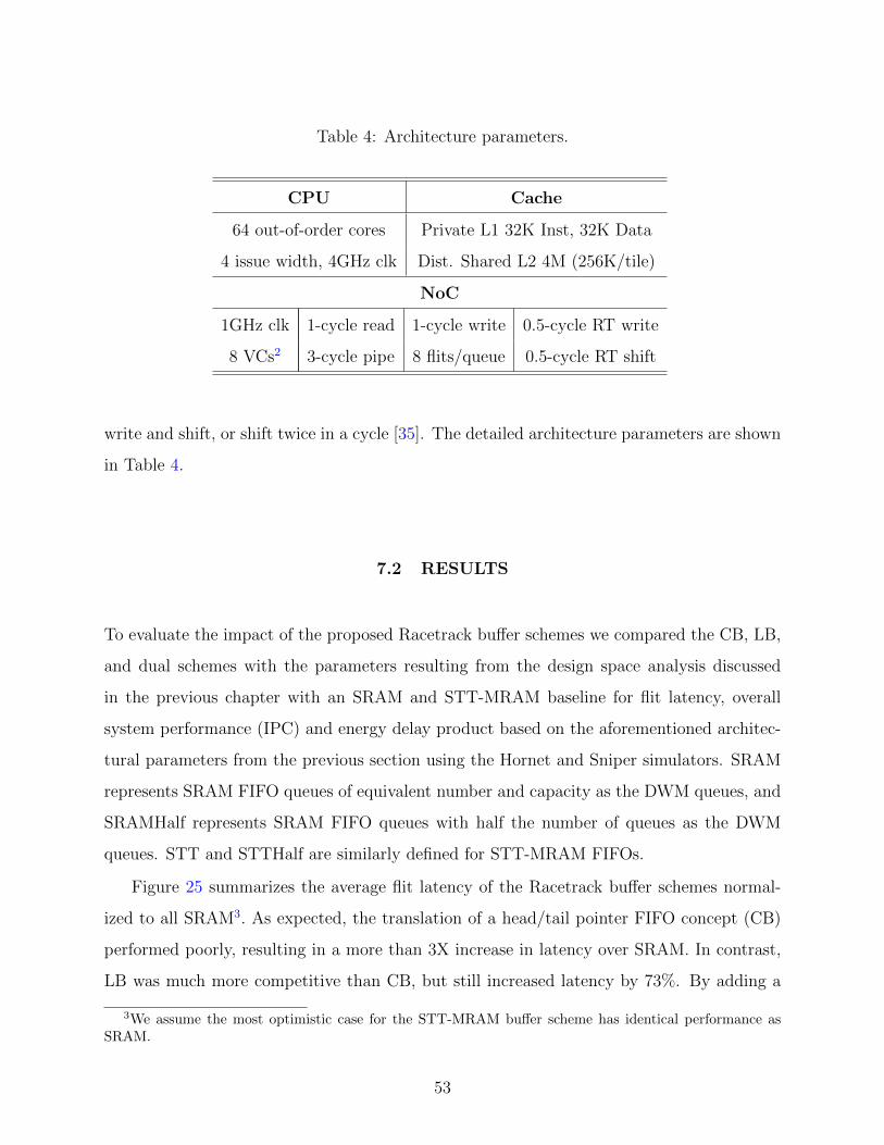
Table 4: Architecture parameters.
CPU Cache
64 out-of-order cores Private L1 32K Inst, 32K Data
4 issue width, 4GHz clk Dist. Shared L2 4M (256K/tile)
NoC
1GHz clk 1-cycle read 1-cycle write 0.5-cycle RT write
8 VCs2 3-cycle pipe 8 flits/queue 0.5-cycle RT shift
write and shift, or shift twice in a cycle [35]. The detailed architecture parameters are shown
in Table 4.
7.2 RESULTS
To evaluate the impact of the proposed Racetrack buffer schemes we compared the CB, LB,
and dual schemes with the parameters resulting from the design space analysis discussed
in the previous chapter with an SRAM and STT-MRAM baseline for flit latency, overall
system performance (IPC) and energy delay product based on the aforementioned architec-
tural parameters from the previous section using the Hornet and Sniper simulators. SRAM
represents SRAM FIFO queues of equivalent number and capacity as the DWM queues, and
SRAMHalf represents SRAM FIFO queues with half the number of queues as the DWM
queues. STT and STTHalf are similarly defined for STT-MRAM FIFOs.
Figure 25 summarizes the average flit latency of the Racetrack buffer schemes normal-
ized to all SRAM3. As expected, the translation of a head/tail pointer FIFO concept (CB)
performed poorly, resulting in a more than 3X increase in latency over SRAM. In contrast,
LB was much more competitive than CB, but still increased latency by 73%. By adding a
3We assume the most optimistic case for the STT-MRAM buffer scheme has identical performance asSRAM.
53

single flit SRAM storage element for the head flit to the Racetrack, the CB (CB+S) and
LB (LB+S) latency overhead can be reduced to 13% and 10% respectively. The SRAM
storage allows the Racetrack FIFO to support a limited number of concurrent reads and
writes reducing the performance overhead of the Racetrack-only approach.
The Dual scheme without adding SRAM actually outperforms the CB+S and LB+S
schemes but still requires an 8% latency overhead compared to the all SRAM FIFO. Dual,
by alternating between two Racetracks, allows most cases of successive reads, writes, and
concurrent reads and writes to be handled without introducing stalls. By adding similar
SRAM storage to Dual (Dual+S), the latency drops to within 2% of the all SRAM case,
which is equivalent to the overhead of reducing the number of SRAM VCs in half.
The impact of these latencies on full system performance is shown in Figure 26 as IPC
normalized to all SRAM buffers. CB resulted in a dramatic 22% IPC degradation, while
LB also had a significant 7.2% IPC reduction compared to SRAM. Adding the SRAM head
flit storage, The LB+S and Dual scheme were nearly indistinguishable, requiring a nominal
1.7% overhead over SRAM and were within 0.5% of the SRAMHalf scheme. Dual+S was
nearly indistinguishable from SRAM.
0.0
0.5
1.0
1.5
Blackscholes Canneal Dedup Ferret Fluidanimate Raytrace Vips X264 Average
Nor
mal
ized
Ener
gy
SRAM SRAMHalf STT STTHalf CB LB Dual CB+S LB+S Dual+S
Figure 27: NoC buffer energy results normalized to SRAM.
The energy consumption of the buffers computed from the information in Table 3 is
shown in Figure 27 and normalized to SRAM. As expected, SRAMHalf, STT, and STTHalf
progressively reduce energy. Of the Racetrack schemes CB does considerably worse than
the other Racetrack schemes despite its reduced static power, while LB and Dual perform
the best. CB+S, LB+S, and Dual+S consume much higher energy due to the added static
54

0.0
0.5
1.0
1.5
2.0
Blackscholes Canneal Dedup Ferret Fluidanimate Raytrace Vips X264 Average
Nor
mal
ized
Ene
rgy-
Del
ay P
rodu
ctSRAM SRAMHalf STT STTHalf CB LB Dual CB+S LB+S Dual+S
9.1 2.93.9 2.4
Figure 28: NoC buffer energy delay product normalized to SRAM.
power from the SRAM, but also because most flits are both written to and read from the
Racetrack and SRAM buffer.
The energy delay product, reported in Figure 28, shows that CB is a poor choice, causing
a more than 2.4X increase over SRAM in energy delay product. LB only provides a 5%
reduction over SRAM, and performs worse than all of the STT-based schemes. However,
Dual has the best result with a more than 35% savings over SRAM and more than 20% over
STT-MRAM. When adding an additional SRAM buffer, CB+S and LB+S are both within
5% of the original SRAM. The Dual+S is better than STT-MRAM implementation by only
3%. The added energy degradation of LB+S and Dual+S make them less valuable than
their non-SRAM buffer counterparts for the energy/performance tradeoff.
55

8.0 CONCLUSIONS
As the drive for system performance through parallelism continues to motivate increasing
number of cores on a chip, the scalability, performance, and energy efficiency of the NoC
becomes a bottleneck for the overall system performance and power consumption. In this
work a high-performance, low-energy multi-hop routing architecture, MSCS, was proposed.
Multi-hop links significantly improve NoC average message latency by allowing flits to tra-
verse multiple hops in a single cycle but require global distributed control. Additional logic
surrounding these links provides the global control necessary to reduce latency and increase
network utilization. By adding reservations to multi-hop links and removing all but one vir-
tual queue per port from the data path, we can reduce the static energy from those queues
while decreasing average in-network latency over the leading multi-hop proposal, SMART.
For benchmark traffic, MSCS results in a 12.7% reduction from SMART with one virtual
channel per port, and a reduction of 1.4% from SMART with two virtual channels per port.
This latter savings is achieved despite the reduced buffer capacity because the reservations
allow a packet to only perform arbitration once for each dimension.
An orthogonal method, aimed primarily at reducing the operational energy of a NoC
by replacing SRAM buffers with intelligently designed DWM queues, was also discussed.
DWM queues provide new control complexities without obvious analogs from constructing
queues using traditional array-based memories. While many different control schemes are
possible, it appears that in all cases for DWM, spending idle cycles to align the leading
data with the read access point (the shift-to-read control strategy) outperforms aligning to
the write access point or staying in place (not proactively shifting). Also, while for LB the
maximum useful shifts in a cycle provides a clear performance ceiling, when the cycle is sized
to the read access latency, one more than the size of the maximum gap between read heads
56

G+ 1 provides a practical ceiling on how many shifts-per-cycle are beneficial. Further, this
read latency-based cycle time limitation results in the saturation region occurring at 50%
reads/writes per cycle, regardless of how many read access points can be included. Increasing
the cycle time to allow shifts before or after a read in a cycle removes this 50% limit for LB,
and would allow the queue to have consistent performance in a system at the cost of reduced
operating frequency. Dual, which does not have the limitation of being unable to perform
consecutive read+write operations, always has a significantly later onset of saturation and
likely can result in a faster operation frequency than LB.
In the context of using DWM to build NoC queues, while the inherent composition
of Racetrack memory can result in a significant energy reduction from traditional SRAM, a
direct replacement of Racetrack memory with well established SRAM FIFO techniques (CB)
results in significantly reduced performance (over 300% increase in message latency without
an SRAM buffer, and 13% on average with an additional SRAM buffer). A conventional
FIFO implementation performs poorly whereas the Dual provided a 56% improvement over
SRAM FIFOs with a nominal performance disadvantage. Due to the reduced number of
read-write heads in DWM as compared to SRAM or STT-MRAM, 2X the number of DWM
queues can occupy the same space as X STT-MRAM queues. When comparing the Dual
results to the configurations with half the number of queues for STT-MRAM or SRAM, Dual
improves the energy-delay product by 17% and 30%, respectively.
57

BIBLIOGRAPHY
[1] R. Venkatesan, M. Sharad, K. Roy, and A. Raghunathan, “DWM-TAPESTRI-an energyefficient all-spin cache using domain wall shift based writes,” Proc. of DATE, pp. 1825–1830, 2013.
[2] W. Zhao et al., “Magnetic domain-wall racetrack memory for high density and fast datastorage,” Proc. of ICSICT, pp. 1–4, IEEE, 2012.
[3] X. Dong, C. Xu, Y. Xie, and N. Jouppi, “NVSim: A Circuit-Level Performance, Energy,and Area Model for Emerging Nonvolatile Memory,” IEEE TCAD, Vol. 31, No. 7,pp. 994–1007, July 2012.
[4] C.-H. O. Chen, S. Park, T. Krishna, S. Subramanian, A. P. Chandrakasan, and L.-S.Peh, “SMART: A single-cycle reconfigurable NoC for SoC applications,” Proc. of DATE,2013, pp. 338–343, March 2013.
[5] H. G. Lee, N. Chang, U. Y. Ogras, and R. Marculescu, “On-chip Communication Archi-tecture Exploration: A Quantitative Evaluation of Point-to-point, Bus, and Network-on-chip Approaches,” ACM Trans. Des. Autom. Electron. Syst., Vol. 12, No. 3, pp. 23:1–23:20, May 2008.
[6] D. Kline Jr, K. Wang, R. Melhem, and A. K. Jones, “Mscs: Multi-hop segmentedcircuit switching,” Proceedings of the 25th edition on Great Lakes Symposium on VLSI,pp. 179–184, ACM, 2015.
[7] S. S. P. Parkin, M. Hayashi, and L. Thomas, “Magnetic Domain-Wall Racetrack Mem-ory,” Science, Vol. 320, No. 5874, pp. 190–194, Apr. 2008.
[8] S. Parkin, “Racetrack Memory: A Storage Class Memory Based on Current ControlledMagnetic Domain Wall Motion,” Proc. of DRC, pp. 3–6, 2009.
[9] D. Kline, H. Xu, R. Melhem, and A. K. Jones, “Domain-wall memory buffer for low-energy NoCs,” Design Automation Conference (DAC), 2015 52nd ACM/EDAC/IEEE,pp. 1–6, IEEE, 2015.
58

[10] F. Jafari, Z. Lu, A. Jantsch, and M. Yaghmaee, “Buffer Optimization in Network-on-Chip Through Flow Regulation,” IEEE TCAD, Vol. 29, No. 12, pp. 1973–1986, Dec2010.
[11] T. Moscibroda and O. Mutlu, “A Case for Bufferless Routing in On-chip Networks,”Proc. of ISCA, ISCA ’09, (New York, NY, USA), pp. 196–207, ACM, 2009.
[12] R. Mullins, A. West, and S. Moore, “The design and implementation of a low-latencyon-chip network,” Proc. of ASPDAC, p. 6 pp., Jan 2006.
[13] G. Michelogiannakis and W. Dally, “Router designs for elastic buffer on-chip networks,”High Performance Computing Networking, Storage and Analysis, Proceedings of theConference on, pp. 1–10, Nov 2009.
[14] P. Zhou, J. Yin, A. Zhai, and S. Sapatnekar, “NoC frequency scaling with flexible-pipeline routers,” Low Power Electronics and Design (ISLPED) 2011 InternationalSymposium on, pp. 403–408, Aug 2011.
[15] A. Kumar, L.-S. Peh, P. Kundu, and N. K. Jha, “Express Virtual Channels: Towardsthe Ideal Interconnection Fabric,” Proc. of ISCA, pp. 150–161, 2007.
[16] N. Jerger, M. Lipasti, and L.-S. Peh, “Circuit-Switched Coherence,” Computer Archi-tecture Letters, Vol. 6, No. 1, pp. 5–8, January 2007.
[17] A. Abousamra, R. Melhem, and A. Jones, “Winning with Pinning in NoC,” Proc. ofHOTI, pp. 13–21, Aug 2009.
[18] Y. Li, A. Abousamra, R. Melhem, and A. Jones, “Compiler-Assisted Data Distributionand Network Configuration for Chip Multiprocessors,” IEEE Trans. on Parallel andDistributed Systems, Vol. 23, No. 11, pp. 2058–2066, Nov 2012.
[19] A. Abousamra, R. Melhem, and A. Jones, “Deja Vu Switching for Multiplane NoCs,”Proc. of NoCS, pp. 11–18, May 2012.
[20] Y. Zhang, W. S. Zhao, D. Ravelosona, J.-O. Klein, J. V. Kim, and C. Chappert,“Perpendicular-magnetic-anisotropy CoFeB racetrack memory,” Journal of AppliedPhysics, Vol. 111, No. 9, No. 9, 2012.
[21] A. Annunziata, M. Gaidis, L. Thomas, C. Chien, C.-C. Hung, P. Chevalier,E. O’Sullivan, J. Hummel, E. Joseph, Y. Zhu, T. Topuria, E. Delenia, P. Rice, S. Parkin,and W. Gallagher, “Racetrack Memory Cell Array with Integrated Magnetic TunnelJunction Readout,” Proc. of IEDM, 2011.
[22] R. Venkatesan, V. Kozhikkottu, C. Augustine, A. Raychowdhury, K. Roy, and A. Raghu-nathan, “TapeCache: a High Density, Energy Efficient Cache based on Domain WallMemory,” Proc. of ISLPED), pp. 185–190, 2012.
59

[23] H. Xu, R. Melhem, and A. K. Jones, “Multilane Racetrack Caches: Improving EfficiencyThrough Compression and Independent Shifting,” Proc. of ASPDAC, 2015.
[24] Y. Zhang, W. Zhao, J.-O. Klein, D. Ravelsona, and C. Chappert, “Ultra-High Den-sity Content Addressable Memory Based on Current Induced Domain Wall Motion inMagnetic Track,” IEEE TMAG, Vol. 48, No. 11, pp. 3219 –3222, Nov. 2012.
[25] R. Nebashi, N. Sakimura, Y. Tsuji, S. Fukami, H. Honjo, S. Saito, S. Miura, N. Ishiwata,K. Kinoshita, T. Hanyu, T. Endoh, N. Kasai, H. Ohno, and T. Sugibayashi, “A ContentAddressable Memory using Magnetic Domain Wall Motion Cells,” Proc. of VLSIC,pp. 300–301, Jun. 2011.
[26] W. Zhao, N. Ben Romdhane, Y. Zhang, J.-O. Klein, and D. Ravelosona, “Racetrackmemory based reconfigurable computing,” Proc. of FTFC, 2013.
[27] M. Mao, W. Wen, Y. Zhang, Y. Chen, and H. H. Li, “Exploration of GPGPU RegisterFile Architecture Using Domain-wall-shift-write based Racetrack Memory,” Proc. ofDAC, pp. 1–6, 2014.
[28] L. Thomas, S.-H. Yang, K.-S. Ryu, B. Hughes, C. Rettner, D.-S. Wang, C.-H. Tsai,K.-H. Shen, and S. Parkin, “Racetrack Memory: A High-performance, Low-cost, Non-volatile Memory based on Magnetic Domain Walls,” Proc. of IEDM, Dec. 2011.
[29] R. Venkatesan, V. Chippa, C. Augustine, K. Roy, and A. Raghunathan, “Energy efficientmany-core processor for recognition and mining using spin-based memory,” NanoscaleArchitectures (NANOARCH), 2011 IEEE/ACM International Symposium on, pp. 122–128, June 2011.
[30] H. Jang, B. S. An, N. Kulkarni, K. H. Yum, and E. J. Kim, “A Hybrid Buffer Designwith STT-MRAM for On-Chip Interconnects,” Proc. of NOCS, pp. 193–200, 2012.
[31] C. Smullen, V. Mohan, A. Nigam, S. Gurumurthi, and M. Stan, “Relaxing non-volatilityfor fast and energy-efficient STT-RAM caches,” Proc. of HPCA, pp. 50–61, Feb 2011.
[32] Z. Sun, X. Bi, H. H. Li, W.-F. Wong, Z.-L. Ong, X. Zhu, and W. Wu, “Multi RetentionLevel STT-RAM Cache Designs with a Dynamic Refresh Scheme,” Proc. of MICRO,pp. 329–338, ACM, 2011.
[33] K.-C. Chang, J.-S. Shen, and T.-F. Chen, “Evaluation and Design Trade-offs BetweenCircuit-switched and Packet-switched NOCs for Application-specific SOCs,” Proceedingsof the 43rd Annual Design Automation Conference, DAC ’06, (New York, NY, USA),pp. 143–148, ACM, 2006.
[34] Z. Sun, X. Bi, A. K. Jones, and H. Li, “Design exploration of racetrack lower-levelcaches,” Proc. of ISLPED, pp. 263–266, ACM, 2014.
60
[35] R. Venkatesan, S. G. Ramasubramanian, S. Venkataramani, K. Roy, and A. Raghu-nathan, “STAG: Spintronic-Tape Architecture for GPGPU cache hierarchies,” Com-puter Architecture (ISCA), 2014 ACM/IEEE 41st International Symposium on, pp. 253–264, IEEE, 2014.
[36] N. Binkert, B. Beckmann, G. Black, S. K. Reinhardt, A. Saidi, A. Basu, J. Hest-ness, D. R. Hower, T. Krishna, S. Sardashti, R. Sen, K. Sewell, M. Shoaib, N. Vaish,M. D. Hill, and D. A. Wood, “The Gem5 Simulator,” SIGARCH Comput. Archit. News,Vol. 39, No. 2, pp. 1–7, Aug. 2011.
[37] “Tilera. TILE-Gx Processor Family. ONLINE.” http://www.tilera.com/products/
processors/TILE-Gx_Family, 2014. [Accessed: December 1, 2014.].
[38] C. Bienia, S. Kumar, J. P. Singh, and K. Li, “The PARSEC benchmark suite: charac-terization and architectural implications,” Proc. of PACT, pp. 72–81, 2008.
[39] S. Woo, M. Ohara, E. Torrie, J. Singh, and A. Gupta, “The SPLASH-2 programs:characterization and methodological considerations,” Proc. of ISCA, pp. 24–36, June1995.
[40] M. Lis, P. Ren, M. H. Cho, K. S. Shim, C. Fletcher, O. Khan, and S. Devadas, “Scalable,accurate multicore simulation in the 1000-core era,” Proceedings of ISPASS, pp. 175–185, April 2011.
[41] T. Carlson, W. Heirman, and L. Eeckhout, “Sniper: Exploring the level of abstractionfor scalable and accurate parallel multi-core simulation,” Proceedings of High Perfor-mance Computing, Networking, Storage and Analysis (SC), pp. 1–12, Nov 2011.
61