Embed Size (px)
Citation preview
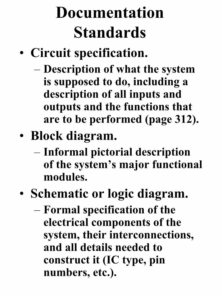
Documentation Standards
• Circuit specification.– Description of what the system
is supposed to do, including a description of all inputs and outputs and the functions that are to be performed (page 312).
• Block diagram.– Informal pictorial description
of the system’s major functional modules.
• Schematic or logic diagram.– Formal specification of the
electrical components of the system, their interconnections, and all details needed to construct it (IC type, pin numbers, etc.).
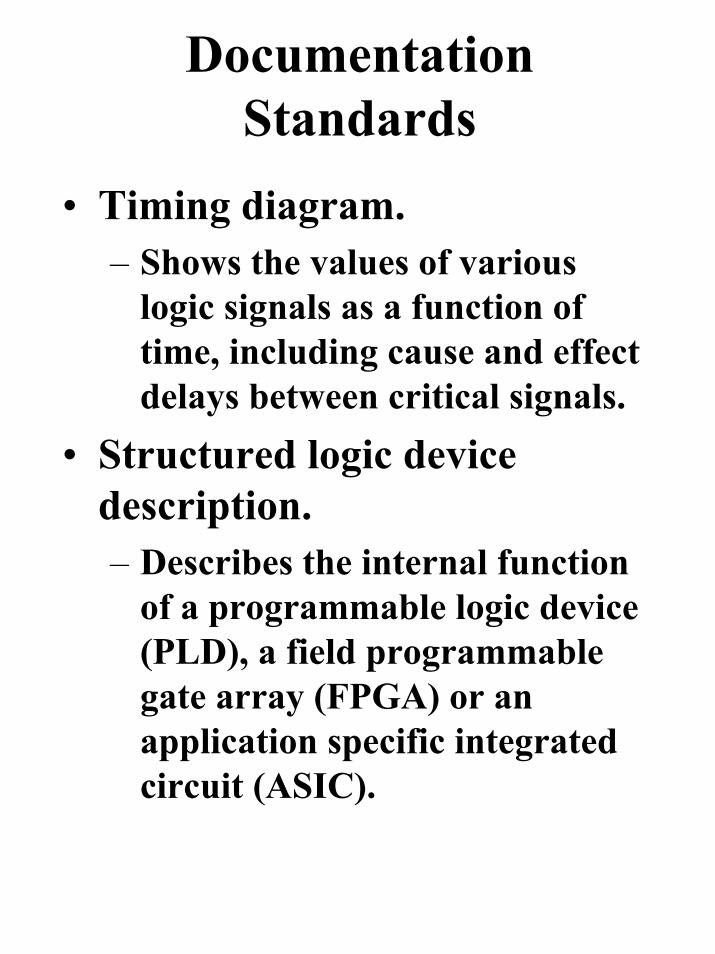
Documentation Standards
• Timing diagram.– Shows the values of various
logic signals as a function of time, including cause and effect delays between critical signals.
• Structured logic device description.– Describes the internal function
of a programmable logic device (PLD), a field programmable gate array (FPGA) or an application specific integrated circuit (ASIC).
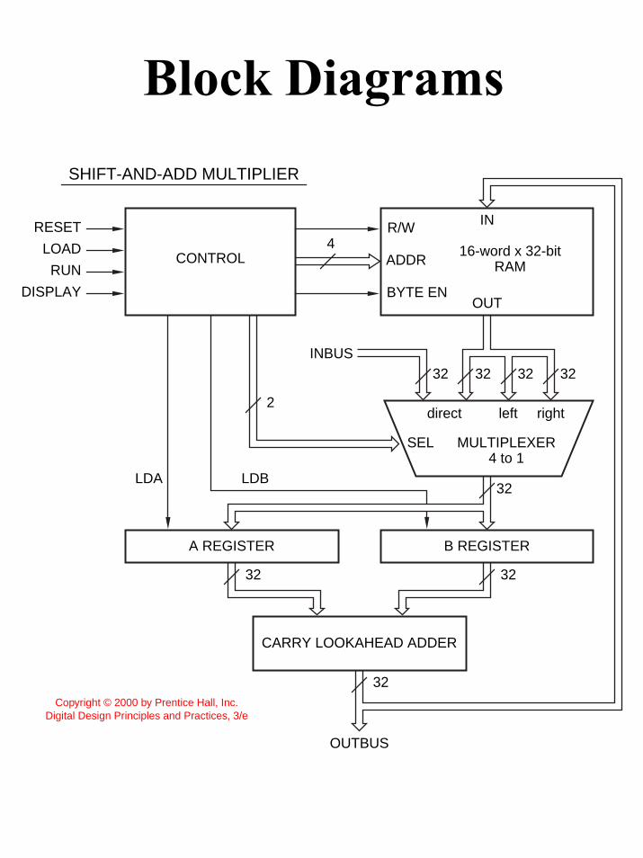
Block Diagrams
R/W
ADDR
BYTE EN
IN
OUT
16-word x 32-bitRAM
CONTROL
RESET
LOAD
RUN
DISPLAY
LDA LDB
4
32
32
32 32 32
A REGISTER B REGISTER
direct left right
INBUS
2
32
32 32
SEL MULTIPLEXER4 to 1
CARRY LOOKAHEAD ADDER
OUTBUS
SHIFT-AND-ADD MULTIPLIER
Copyright © 2000 by Prentice Hall, Inc.Digital Design Principles and Practices, 3/e
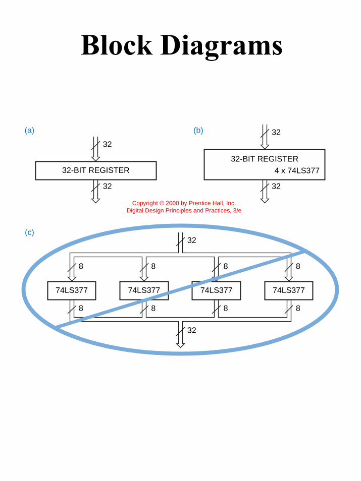
Block Diagrams
32
32
32
8
8
8
8
8
8
8
8
32-BIT REGISTER
32
32
32-BIT REGISTER
32
4 x 74LS377
(a)
(c)
(b)
74LS377 74LS377 74LS377 74LS377
Copyright © 2000 by Prentice Hall, Inc.Digital Design Principles and Practices, 3/e
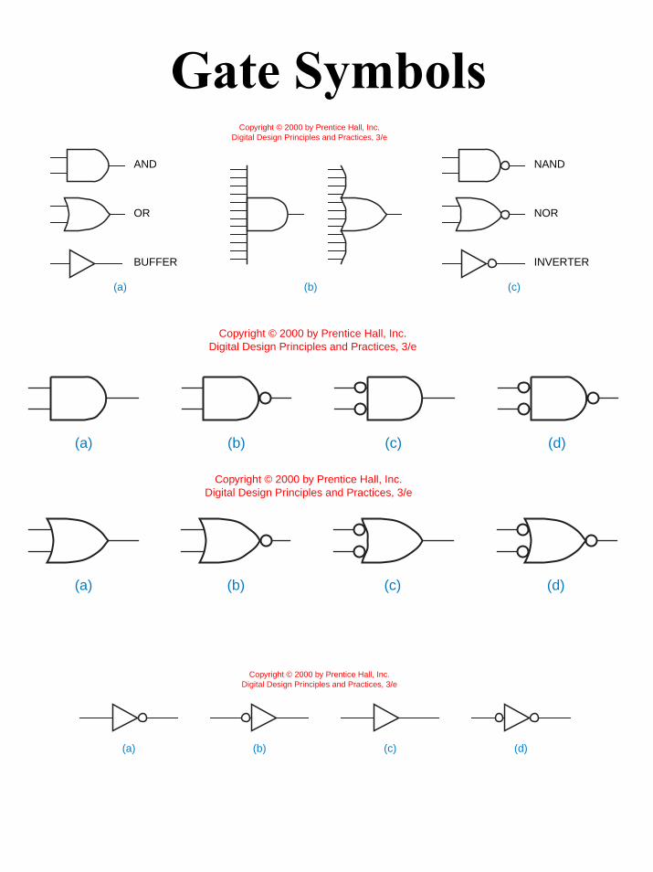
Gate SymbolsAND
OR
BUFFER
(a)
NAND
NOR
INVERTER
(c)(b)
Copyright © 2000 by Prentice Hall, Inc.Digital Design Principles and Practices, 3/e
(a) (b) (c) (d)
Copyright © 2000 by Prentice Hall, Inc.Digital Design Principles and Practices, 3/e
(a) (b) (c) (d)
Copyright © 2000 by Prentice Hall, Inc.Digital Design Principles and Practices, 3/e
(a) (b) (c) (d)
Copyright © 2000 by Prentice Hall, Inc.Digital Design Principles and Practices, 3/e
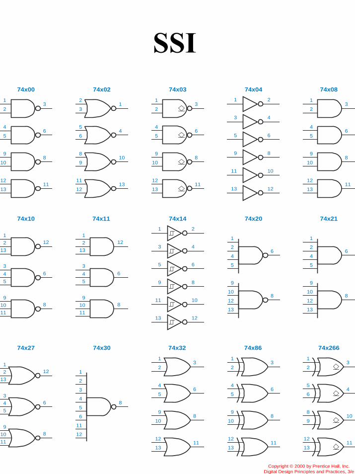
SSI74x00
74x10 74x11
74x02
74x27
74x04 74x08
74x14 74x20
74x30
74x21
74x32
74x03
74x86
12
1311
9
108
4
56
1
23
1
2
13
12
3
4
5
6
9
10
11
8
1
2
13
12
3
4
5
6
9
10
11
8
11
1213
8
910
5
64
2
31
1
2
13
12
3
4
5
6
9
10
11
8
9 8
5 6
3 4
1 2
13 12
11 10
12
1311
9
108
4
56
1
23
9 8
5 6
3 4
1 2
13 12
11 10
2
1
4
5
6
10
9
12
13
8
4
3
2
1
5
6
11
12
8
2
1
4
5
6
10
9
12
13
8
12
1311
9
108
4
56
1
23
12
1311
9
108
4
56
1
23
12
1311
9
108
4
56
1
23
12
1311
8
910
5
64
1
23
74x266
Copyright © 2000 by Prentice Hall, Inc.Digital Design Principles and Practices, 3/e
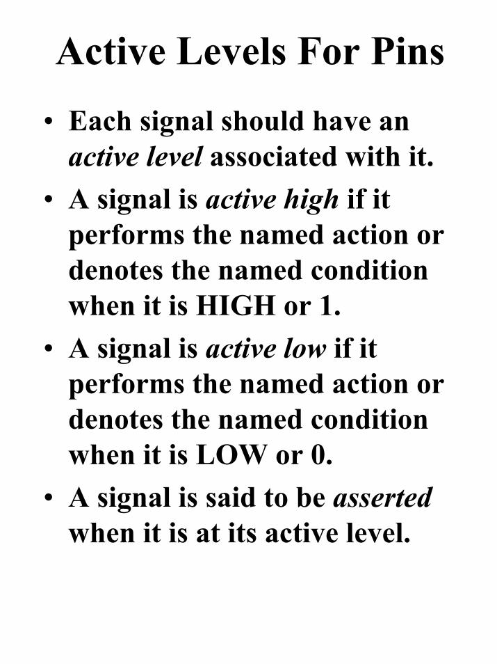
Active Levels For Pins• Each signal should have an
active level associated with it.• A signal is active high if it
performs the named action or denotes the named condition when it is HIGH or 1.
• A signal is active low if it performs the named action or denotes the named condition when it is LOW or 0.
• A signal is said to be assertedwhen it is at its active level.
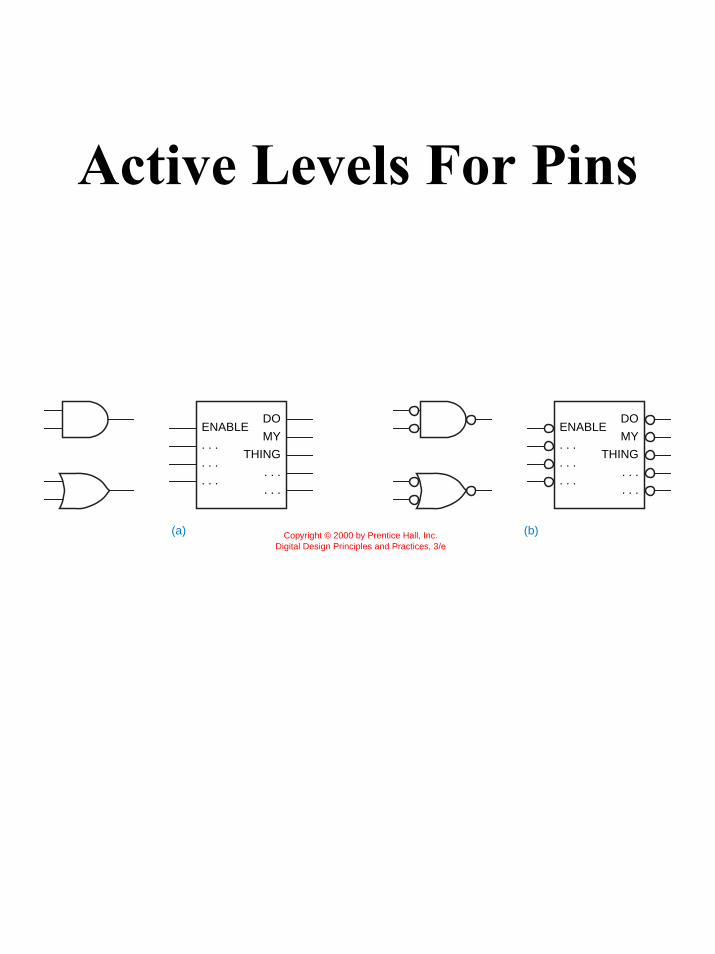
Active Levels For Pins
ENABLE
. . .
. . .
. . .
DO
MY
THING
. . .
. . .
ENABLE
. . .
. . .
. . .
DO
MY
THING
. . .
. . .
(a) (b)Copyright © 2000 by Prentice Hall, Inc.Digital Design Principles and Practices, 3/e
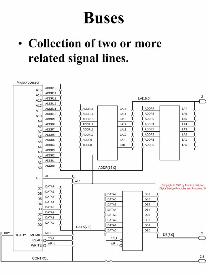
Buses• Collection of two or more
related signal lines.
Microprocessor
A15
A14
A13
A12
A11
A10
A9
A8
A7
A6
A5
A4
A3
A2
A1
A0
ALE
ADDR15
ADDR14
ADDR13
ADDR12
ADDR11
ADDR10
ADDR9
ADDR8
ADDR8
ADDR7
ADDR6
ADDR5
ADDR4
ADDR3
ADDR2
ADDR1
ADDR0
ALE
ALE
ADDR15 LA15
LA14
LA13
LA12
LA11
LA10
LA7
LA8
ADDR14
ADDR13
ADDR12
ADDR11
ADDR10
ADDR9
D7DATA7
DATA6
DATA5
DATA4
DATA3
DATA2
DATA1
DATA0
D6
D5
D4
D3
D2
D1
D0
MIORDYMEMIO
RD_LREAD
WR_L
RD_L
WR_LWRITE
CONTROL
DATA[7:0]
ADDR[15:0]
LA[15:0]
DB[7:0]
DATA7
DATA6
DATA5
DATA4
DATA3
DATA2
DATA1
DATA0
DB7
DB6
DB5
DB4
DB3
DB2
DB1
DB0
READY
LA7
LA6
LA5
LA4
LA3
LA2
LA1
LA0
ADDR7
ADDR6
ADDR5
ADDR4
ADDR3
ADDR2
ADDR1
ADDR0
2,3
2
2
Copyright © 2000 by Prentice Hall, Inc.Digital Design Principles and Practices, 3/e
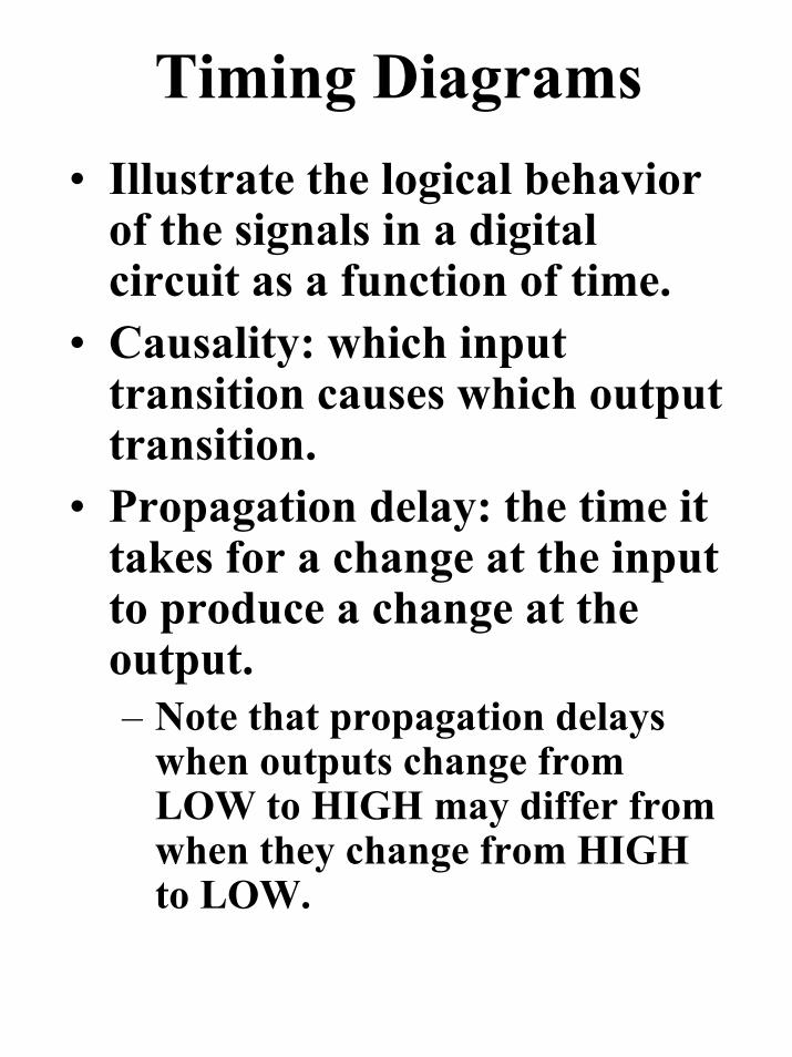
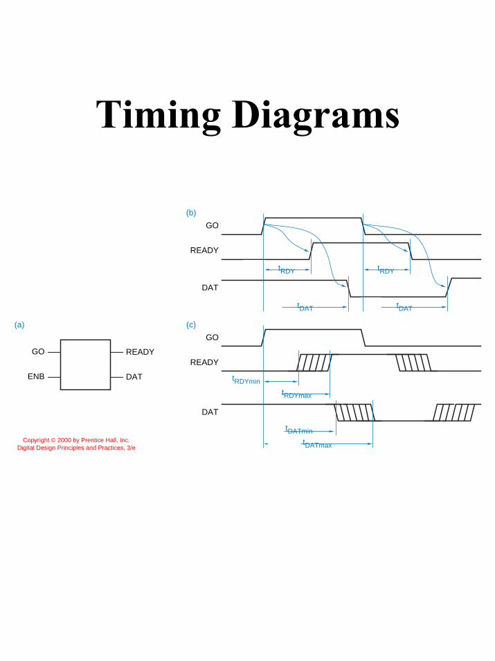
Timing Diagrams• Illustrate the logical behavior
of the signals in a digital circuit as a function of time.
• Causality: which input transition causes which output transition.
• Propagation delay: the time it takes for a change at the input to produce a change at the output.– Note that propagation delays
when outputs change from LOW to HIGH may differ from when they change from HIGH to LOW.
Timing Diagrams
GO
READY
DAT
(b)
GO
READY
DAT
(c)(a)
t
GO
ENB
READY
DAT
DAT
RDY
RDYmin
DATmax
DATmin
RDYmax
DAT
RDY
t
t
t
t
t t
t
Copyright © 2000 by Prentice Hall, Inc.Digital Design Principles and Practices, 3/e
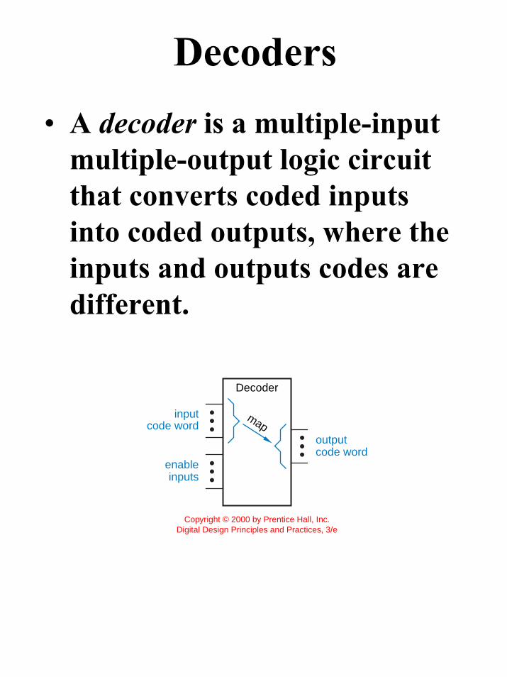
Decoders• A decoder is a multiple-input
multiple-output logic circuit that converts coded inputs into coded outputs, where the inputs and outputs codes are different.
Decoder
inputcode word
enableinputs
outputcode word
map
Copyright © 2000 by Prentice Hall, Inc.Digital Design Principles and Practices, 3/e
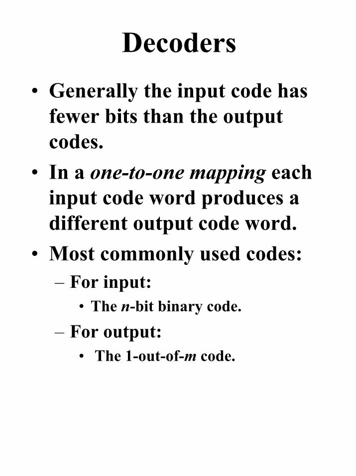
Decoders• Generally the input code has
fewer bits than the output codes.
• In a one-to-one mapping each input code word produces a different output code word.
• Most commonly used codes:– For input:• The n-bit binary code.
– For output:• The 1-out-of-m code.
Binary Decoder• Binary decoder:– The most common decoder.– n-to-2n.– The input code is the n-bit
binary code.– The output code is the 1-out-of-
m code.
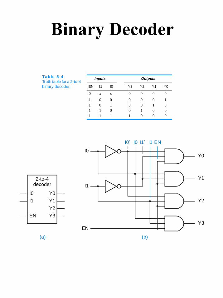
Binary Decoder
Table 5 -4Truth table for a 2-to-4 binary decoder.
Inputs Outputs
EN I1 I0 Y3 Y2 Y1 Y0
0 x x 0 0 0 0
1 0 0 0 0 0 1 1 0 1 0 0 1 0 1 1 0 0 1 0 0 1 1 1 1 0 0 0
2-to-4decoder
I0
I1
EN
Y0
Y1
Y2
Y3
(a) (b)
I0′ I0 I1′ I1 EN
I0
I1
EN
Y0
Y1
Y2
Y3
Binary DecoderTable 5-6Truth table for one-half of a 74x139 dual 2-to-4 decoder.
Inputs Outputs
G_L B A Y3_L Y2_L Y1_L Y0_L
1 x x 1 1 1 10 0 0 1 1 1 00 0 1 1 1 0 10 1 0 1 0 1 10 1 1 0 1 1 1
74x139
1A
1G
1B
1Y0
1Y1
1Y2
1Y3
(b)
1G_L
1A
1B
(1)
(4)
1 4
5
6
7
2
3
2A
2G
2B
2Y0
2Y1
2Y2
2Y3
15 12
11
10
9
14
13
1/2 74x139
A
G
B
Y0
Y1
Y2
Y3
(c)
(5)
(6)
(7)
(2)
(3)
1Y0_L
1Y1_L
1Y2_L
1Y3_L
2G_L
2A
2B
(15)
(12)
(11)
(10)
(9)
(14)
(13)
2Y0_L
2Y1_L
2Y2_L
2Y3_L
(a)
Copyright © 2000 by Prentice Hall, Inc.Digital Design Principles and Practices, 3/e
1/2 74x139
A
G
B
Y0
Y1
Y2
Y3
(a) (b)
1/2 74x139
A
G
B
Y0
Y1
Y2
Y3
Copyright © 2000 by Prentice Hall, Inc.Digital Design Principles and Practices, 3/e
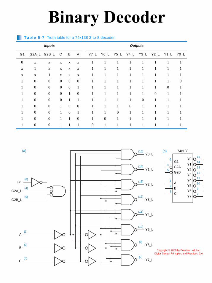
Binary DecoderTable 5-7 Truth table for a 74x138 3-to-8 decoder.
Inputs Outputs
G1 G2A_L G2B_L C B A Y7_L Y6_L Y5_L Y4_L Y3_L Y2_L Y1_L Y0_L
0 x x x x x 1 1 1 1 1 1 1 1
x 1 x x x x 1 1 1 1 1 1 1 1
x x 1 x x x 1 1 1 1 1 1 1 1
1 0 0 0 0 0 1 1 1 1 1 1 1 0
1 0 0 0 0 1 1 1 1 1 1 1 0 1
1 0 0 0 1 0 1 1 1 1 1 0 1 1
1 0 0 0 1 1 1 1 1 1 0 1 1 1
1 0 0 1 0 0 1 1 1 0 1 1 1 1
1 0 0 1 0 1 1 1 0 1 1 1 1 1
1 0 0 1 1 0 1 0 1 1 1 1 1 1
1 0 0 1 1 1 0 1 1 1 1 1 1 1
74x138
G2A
G1
G2B
Y0
Y1
Y2
Y3
(b)(15)
615
14
13
7
4
5
B
A
C
Y4
Y5
Y6
Y7
1
12
11
10
92
3
(14)
(13)
(12)
Y0_L
Y1_L
Y2_L
Y3_L
C
(11)
(10)
(9)
(7)(3)
B(2)
Y4_L
Y5_L
Y6_L
Y7_L
A(1)
G2B_L(5)
G2A_L(4)
G1(6)
(a)
Copyright © 2000 by Prentice Hall, Inc.Digital Design Principles and Practices, 3/e
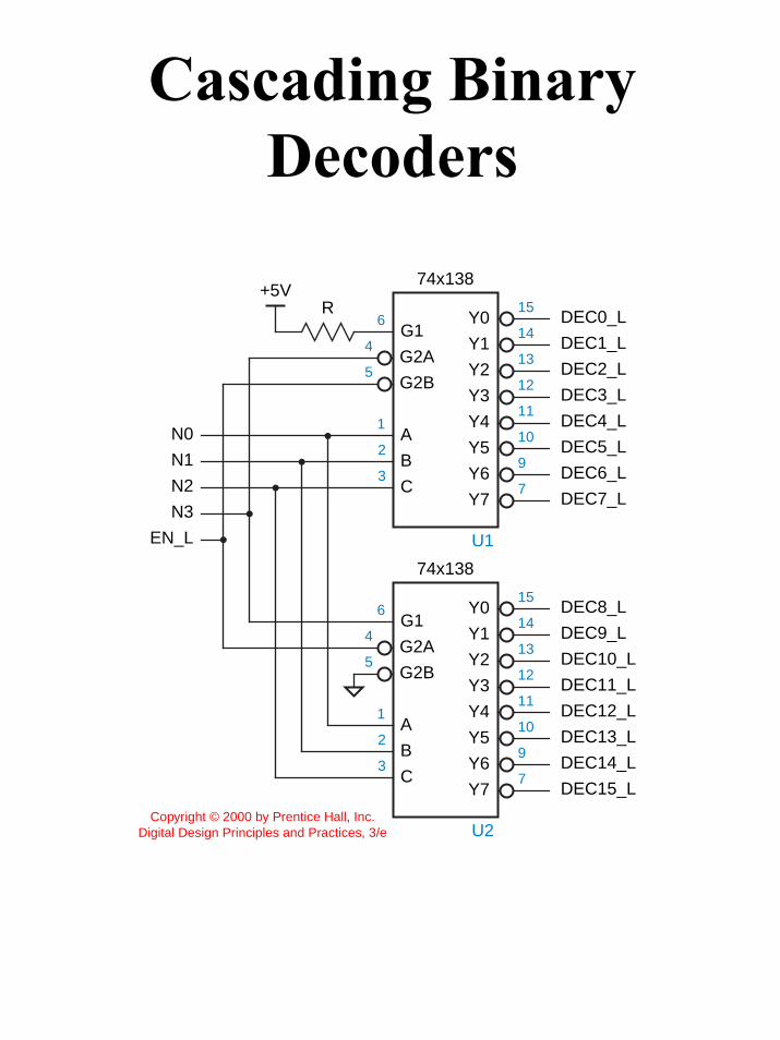
Cascading Binary Decoders
74x138
G2A
G1
G2B
Y0
Y1
Y2
Y3
615
14
13
7
4
5
B
A
C
Y4
Y5
Y6
Y7
1
12
11
10
92
3
74x138
G2A
G1
G2B
Y0
Y1
Y2
Y3
615
14
13
7
4
5
B
A
C
Y4
Y5
Y6
Y7
1
12
11
10
92
3
DEC0_L
DEC1_L
DEC2_L
DEC3_L
DEC4_L
DEC5_L
DEC10_L
DEC11_L
DEC12_L
DEC13_L
DEC14_L
DEC15_L
DEC6_L
DEC7_L
DEC8_L
DEC9_L
N0
N1
N2
N3
EN_L
+5V
U1
U2
R
Copyright © 2000 by Prentice Hall, Inc.Digital Design Principles and Practices, 3/e
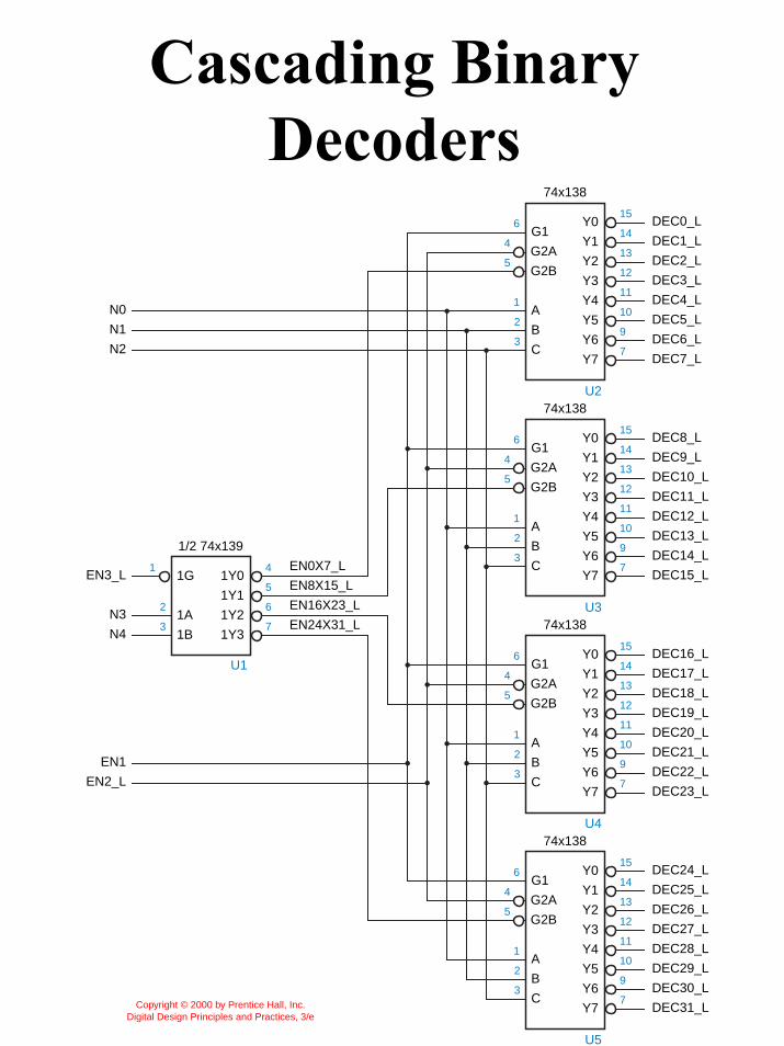
Cascading Binary Decoders
74x138
G2A
G1
G2B
Y0
Y1
Y2
Y3
B
A
C
Y4
Y5
Y6
Y7
74x138
G2A
G1
G2B
Y0
Y1
Y2
Y3
B
A
C
Y4
Y5
Y6
Y7
DEC0_L
DEC1_L
DEC2_L
DEC3_L
DEC4_L
DEC5_L
DEC10_L
DEC11_L
DEC12_L
DEC13_L
DEC14_L
DEC15_L
DEC6_L
DEC7_L
DEC8_L
DEC9_L
N0
N1
N2
N3
EN3_L
N4
EN2_L
EN1
74x138
G2A
G1
G2B
Y0
Y1
Y2
Y3
B
A
C
Y4
Y5
Y6
Y7
DEC18_L
DEC19_L
DEC20_L
DEC21_L
DEC22_L
DEC23_L
DEC16_L
DEC17_L
74x138
G2A
G1
G2B
Y0
Y1
Y2
Y3
B
A
C
Y4
Y5
Y6
Y7
DEC26_L
DEC27_L
DEC28_L
DEC29_L
DEC30_L
DEC31_L
DEC24_L
DEC25_L
1/2 74x139
1A
1G
1B
1Y0
1Y1
1Y2
1Y3
EN0X7_L
EN8X15_L
EN16X23_L
EN24X31_L
615
14
13
7
4
5
1
12
11
10
92
3
615
14
13
7
4
5
1
12
11
10
92
3
615
14
13
7
4
5
1
12
11
10
92
3
615
14
13
7
4
5
1
12
11
10
92
3
1 4
5
6
7
2
3
U2
U3
U4
U5
U1
Copyright © 2000 by Prentice Hall, Inc.Digital Design Principles and Practices, 3/e
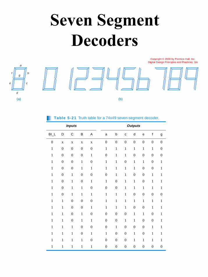
Seven Segment Decoders
a
b
ce
f
d
g
(a) (b)
Copyright © 2000 by Prentice Hall, Inc.Digital Design Principles and Practices, 3/e
Table 5-21 Truth table for a 74x49 seven-segment decoder.
Inputs Outputs
BI_L D C B A a b c d e f g
0 x x x x 0 0 0 0 0 0 0
1 0 0 0 0 1 1 1 1 1 1 0
1 0 0 0 1 0 1 1 0 0 0 0
1 0 0 1 0 1 1 0 1 1 0 1
1 0 0 1 1 1 1 1 1 0 0 1
1 0 1 0 0 0 1 1 0 0 1 1
1 0 1 0 1 1 0 1 1 0 1 1
1 0 1 1 0 0 0 1 1 1 1 1
1 0 1 1 1 1 1 1 0 0 0 0
1 1 0 0 0 1 1 1 1 1 1 1
1 1 0 0 1 1 1 1 0 0 1 1
1 1 0 1 0 0 0 0 1 1 0 1
1 1 0 1 1 0 0 1 1 0 0 1
1 1 1 0 0 0 1 0 0 0 1 1
1 1 1 0 1 1 0 0 1 0 1 1
1 1 1 1 0 0 0 0 1 1 1 1
1 1 1 1 1 0 0 0 0 0 0 0
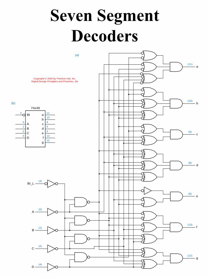
Seven Segment Decoders
(3)
(4)
(11)a
(10)b
(9)c
(8)d
(13)f
BI_L
D
(2)C
(1)B
(5)A
(6)e
(12)g
74x49
BI
A
a
b
3 11
10
c9
d8
e6
f13
g12
5
B
C
1
2
D4
(b)
(a)
Copyright © 2000 by Prentice Hall, Inc.Digital Design Principles and Practices, 3/e
Encoders• Reverses what a decoder does.• If a device’s output code word
has fewer bits than the input code word then the device is usually called an encoder.
• The simplest encoder is the binary encoder or the 2n-to-nencoder.
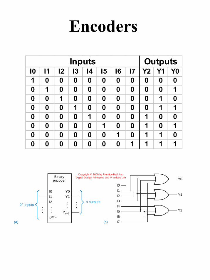
Encoders
I0 I1 I2 I3 I4 I5 I6 I7 Y2 Y1 Y01 0 0 0 0 0 0 0 0 0 00 1 0 0 0 0 0 0 0 0 10 0 1 0 0 0 0 0 0 1 00 0 0 1 0 0 0 0 0 1 10 0 0 0 1 0 0 0 1 0 00 0 0 0 0 1 0 0 1 0 10 0 0 0 0 0 1 0 1 1 00 0 0 0 0 0 0 1 1 1 1
Inputs Outputs
Binaryencoder
Y0
Y1I1
I0
I2
I2n–1
Yn–1
2n inputsn outputs
(a) (b)
I0
I1
I2
I3
I4
I5
I6
I7
Y0
Y1
Y2
Copyright © 2000 by Prentice Hall, Inc.Digital Design Principles and Practices, 3/e
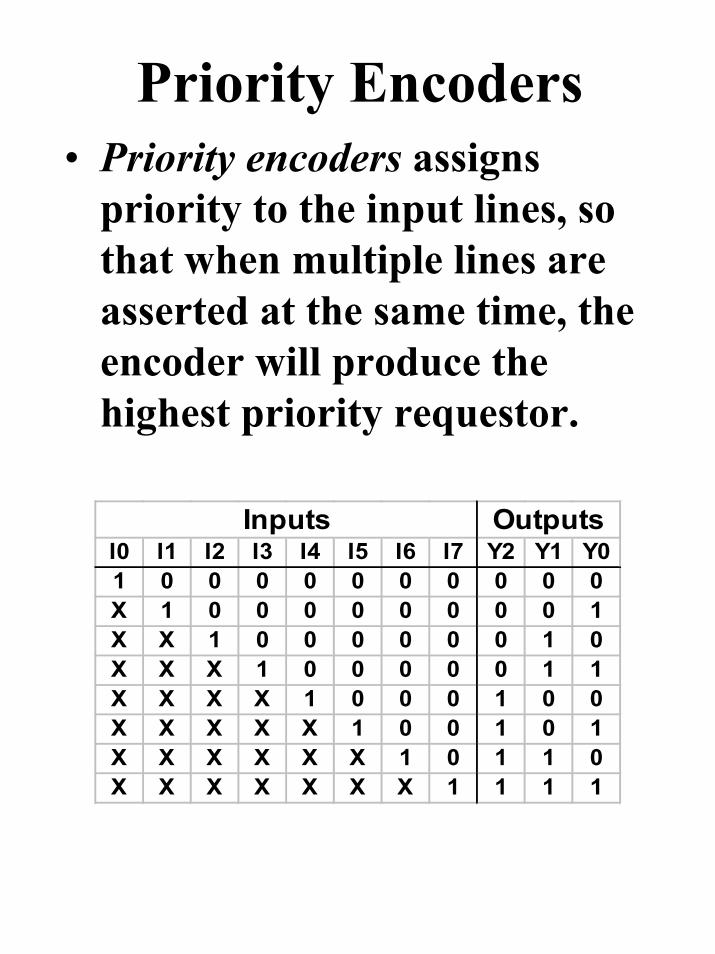
Priority Encoders• Priority encoders assigns
priority to the input lines, so that when multiple lines are asserted at the same time, the encoder will produce the highest priority requestor.
I0 I1 I2 I3 I4 I5 I6 I7 Y2 Y1 Y01 0 0 0 0 0 0 0 0 0 0X 1 0 0 0 0 0 0 0 0 1X X 1 0 0 0 0 0 0 1 0X X X 1 0 0 0 0 0 1 1X X X X 1 0 0 0 1 0 0X X X X X 1 0 0 1 0 1X X X X X X 1 0 1 1 0X X X X X X X 1 1 1 1
Inputs Outputs
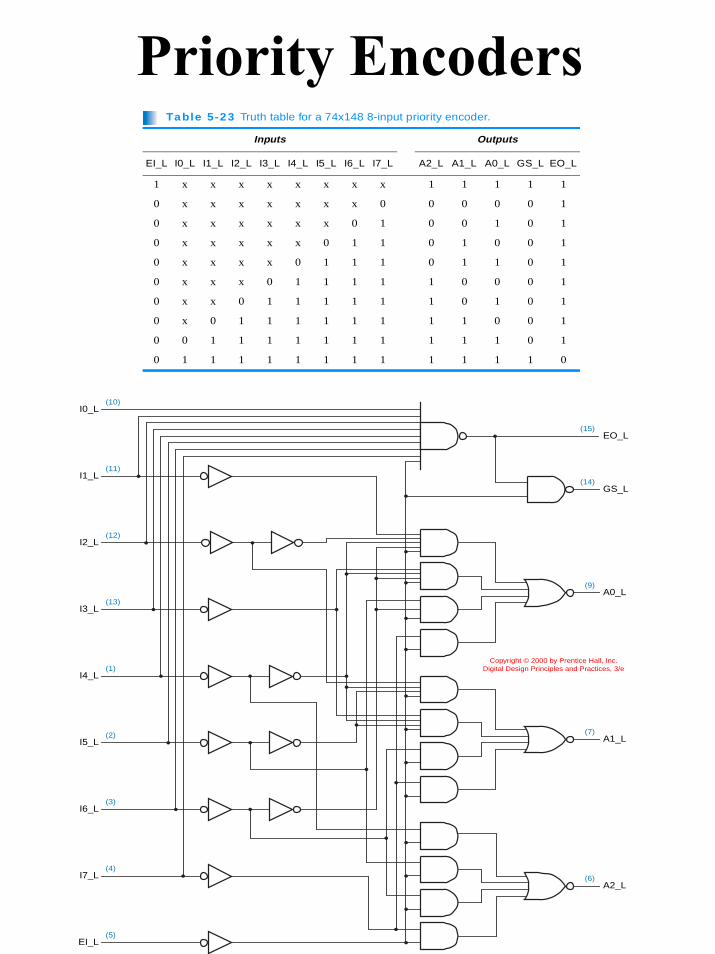
Priority EncodersTable 5-23 Truth table for a 74x148 8-input priority encoder.
Inputs Outputs
EI_L I0_L I1_L I2_L I3_L I4_L I5_L I6_L I7_L A2_L A1_L A0_L GS_L EO_L
1 x x x x x x x x 1 1 1 1 1
0 x x x x x x x 0 0 0 0 0 1
0 x x x x x x 0 1 0 0 1 0 1
0 x x x x x 0 1 1 0 1 0 0 1
0 x x x x 0 1 1 1 0 1 1 0 1
0 x x x 0 1 1 1 1 1 0 0 0 1
0 x x 0 1 1 1 1 1 1 0 1 0 1
0 x 0 1 1 1 1 1 1 1 1 0 0 1
0 0 1 1 1 1 1 1 1 1 1 1 0 1
0 1 1 1 1 1 1 1 1 1 1 1 1 0
(10)
(11)
(12)
(13)
(1)
(2)
(3)
(4)
(5)EI_L
I7_L
I6_L
I5_L
I4_L
I3_L
I2_L
I1_L
I0_L
EO_L
GS_L
A0_L
A1_L
A2_L(6)
(7)
(9)
(14)
(15)
Copyright © 2000 by Prentice Hall, Inc.Digital Design Principles and Practices, 3/e
Cascading Binary Encoders
I7
I6
I5I4
I3
I2
I1
I0
A2
A1
A0
GS
EO
EI
6
7
9
14
15
10
11
12
13
1
2
3
4
5
74x148
I7
I6
I5I4
I3
I2
I1
I0
A2
A1
A0
GS
EO
EI
6
7
9
14
15
10
11
12
13
1
2
3
4
5
74x148
I7
I6
I5I4
I3
I2
I1
I0
A2
A1
A0
GS
EO
EI
6
7
9
14
15
10
11
12
13
1
2
3
4
5
74x148
74x148
REQ31_L
REQ30_L
REQ29_L
REQ28_L
REQ27_L
REQ26_L
REQ25_L
REQ24_L
REQ23_L
REQ22_L
REQ21_L
REQ20_L
REQ19_L
REQ18_L
REQ17_L
REQ16_L
REQ15_L
REQ14_L
REQ13_L
REQ12_L
REQ11_L
REQ10_L
REQ9_L
REQ8_L
REQ0_L
REQ1_L
REQ2_L
REQ3_L
REQ4_L
REQ5_L
REQ6_L
REQ7_L I7
I6
I5I4
I3
I2
I1
I0
A2
A1
A0
GS
EO
EI
6
7
9
14
15
10
11
12
13
1
2
3
4
5
RGS
RA0
RA1
RA2
RA3
RA4
U1
U2
U3
U4
G3A2_L
G3A1_L
G3A0_L
G3GS_L
G3EO_L
G2A2_L
G2A1_L
G2A0_L
G2GS_L
G2EO_L
G1A2_L
G1A1_L
G1A0_L
G1GS_L
G1EO_L
G0A2_L
G0A1_L
G0A0_L
G0GS_L
74x001
23
U5
74x004
56
U5
74x20
U7
9
10
128
13
74x20
U7
1
2
46
5
74x20
U6
9
10
128
13
74x20
U6
1
2
46
5
Copyright © 2000 by Prentice Hall, Inc.Digital Design Principles and Practices, 3/e
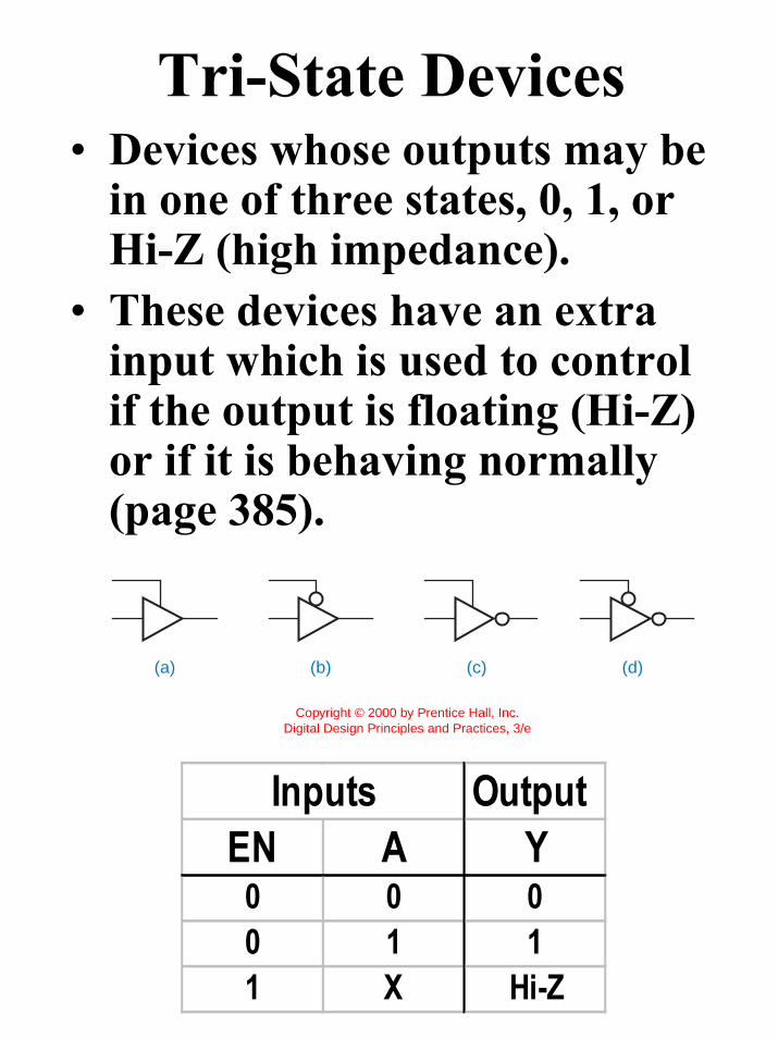
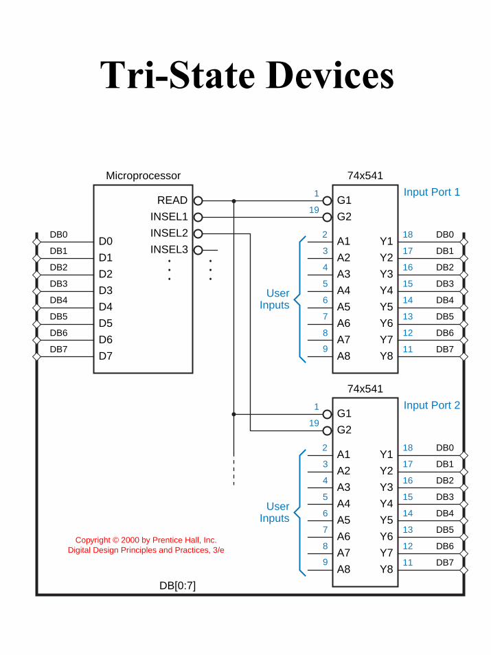
Tri-State Devices• Devices whose outputs may be
in one of three states, 0, 1, or Hi-Z (high impedance).
• These devices have an extra input which is used to control if the output is floating (Hi-Z) or if it is behaving normally (page 385).
(a) (b) (c) (d)
Copyright © 2000 by Prentice Hall, Inc.Digital Design Principles and Practices, 3/e
OutputEN A Y0 0 00 1 11 X Hi-Z
Inputs
Tri-State Devices
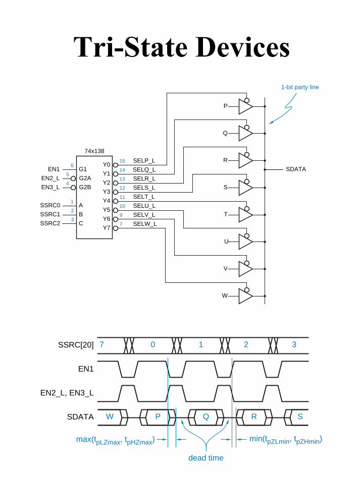
SELP_L
SELQ_L
SELR_L
SELS_L
SELT_L
SELU_L
SELV_L
SELW_L
SDATAEN1
EN2_L
EN3_L
SSRC0
SSRC1
SSRC2
P
1-bit party line
Q
R
S
T
U
V
W
74x138
G2A
G1
G2B
Y0
Y1
Y2
Y3
6
5
4
15
14
13
7
B
A
C
Y4
Y5
Y6
Y7
1
12
11
10
92
3
07SSRC[20]
EN1
EN2_L, EN3_L
1 2 3
SDATA P Q R SW
max(tpLZmax, tpHZmax) min(tpZLmin, tpZHmin)
dead time
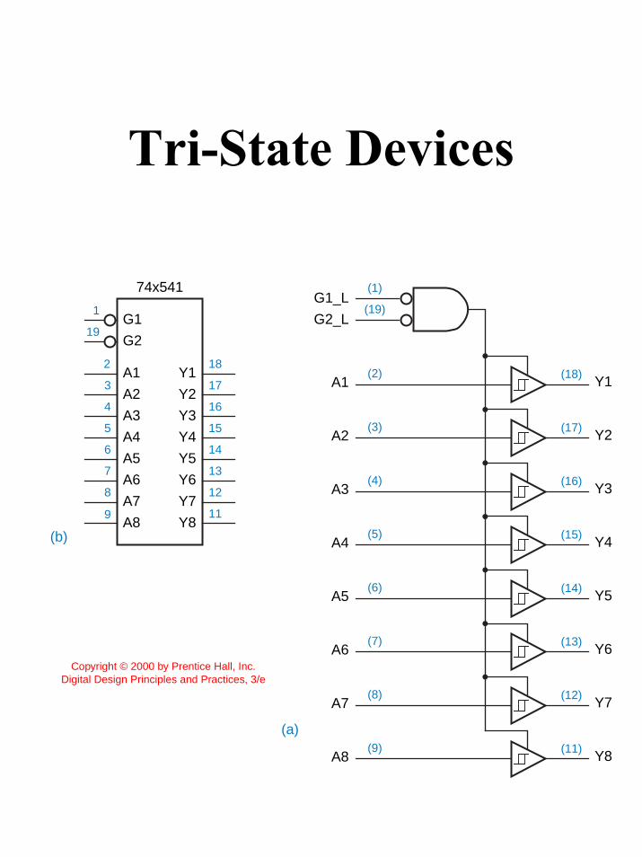
Tri-State Devices
74x541
G2
G1
Y1
Y2
Y3
(b)
(a)
1
19
15
14
16
17
18
13
A1
A2
A3
A4
A5
A6
A7
A8
Y4
Y5
Y6
Y7
Y8
2
12
11
3
4
5
6
7
8
9
(18)Y1
(1)
(19)
(2)
(17)Y2
(3)
(16)Y3
(4)
(15)Y4
(5)
(14)Y5
(6)
(13)Y6
(7)
(12)Y7
(8)
(11)Y8
G1_L
G2_L
A1
A2
A3
A4
A5
A6
A7
A8(9)
Copyright © 2000 by Prentice Hall, Inc.Digital Design Principles and Practices, 3/e
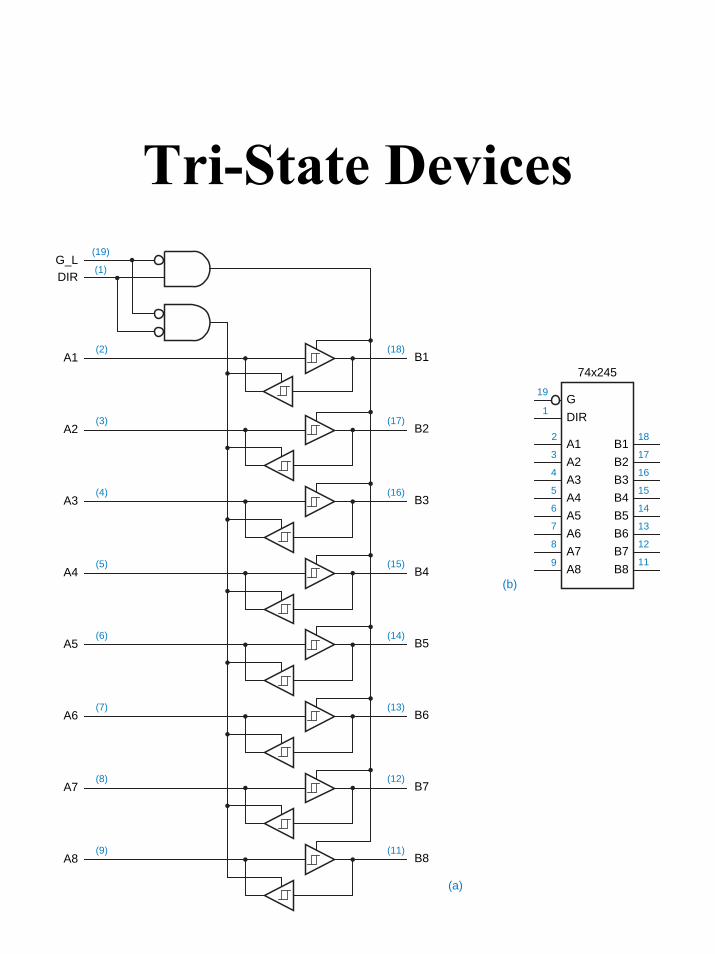
Tri-State Devices
74x245
DIR
G
B1
B2
B3
(b)
(a)
19
1
15
14
16
17
18
13
A1
A2
A3
A4
A5
A6
A7
A8
B4
B5
B6
B7
B8
2
12
11
3
4
5
6
7
8
9
(18)B1
G_L(19)
DIR(1)
A1(2)
(17)B2A2
(3)
(16)B3A3
(4)
(15)B4A4
(5)
(14)B5A5
(6)
(13)B6A6
(7)
(12)B7A7
(8)
(11)B8A8
(9)
Tri-State Devices
74x541
G2
G1
Y1
Y2
Y3
1
19
15
14
16
17
18 DB0
DB1
DB2
DB3
DB4
DB5
DB6
DB0
DB1
DB2
DB3
DB4
DB5
DB6
DB7DB7
DB0
DB1
DB2
DB3
DB4
DB5
DB6
DB7
13
A1
A2
A3
A4
A5
A6
A7
A8
Y4
Y5
Y6
Y7
Y8
2
12
11
3
4
5
6
7
8
Microprocessor
READ
INSEL1
INSEL2D0
D1
D2
D3
D4
D5
D6
DB[0:7]
D7
INSEL3
9
74x541
G2
G1
Y1
Y2
Y3
1
19
15
14
16
17
18
13
A1
A2
A3
A4
A5
A6
A7
A8
Y4
Y5
Y6
Y7
Y8
2
12
11
3
4
5
6
7
8
9
Input Port 1
Input Port 2
User Inputs
User Inputs
Copyright © 2000 by Prentice Hall, Inc.Digital Design Principles and Practices, 3/e
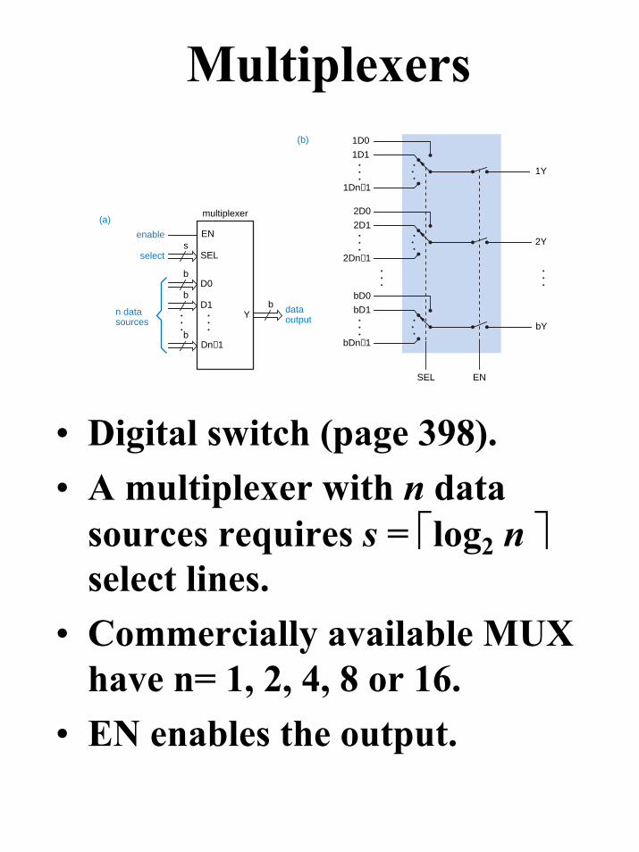
Multiplexers
multiplexer
EN
SELs
enable
select
D0b
bD1b
Dn−1b
n datasources
(a)
(b)
dataoutputY
1D0
1D1
1Dn−1
2D0
2D1
2Dn−1
bD0
bD1
bDn−1
1Y
2Y
bY
SEL EN
• Digital switch (page 398).• A multiplexer with n data
sources requires s = log2 n select lines.
• Commercially available MUX have n= 1, 2, 4, 8 or 16.
• EN enables the output.
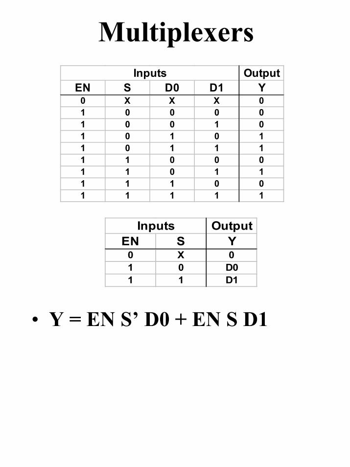
MultiplexersOutput
EN S D0 D1 Y0 X X X 01 0 0 0 01 0 0 1 01 0 1 0 11 0 1 1 11 1 0 0 01 1 0 1 11 1 1 0 01 1 1 1 1
Inputs
OutputEN S Y0 X 01 0 D01 1 D1
Inputs
• Y = EN S’ D0 + EN S D1
Multiplexers
∑−
=
⋅⋅=1
0iDMENiY
n
jjj
multiplexer
EN
SELs
enable
select
D0b
bD1b
Dn−1b
n datasources
(a)
(b)
dataoutputY
1D0
1D1
1Dn−1
2D0
2D1
2Dn−1
bD0
bD1
bDn−1
1Y
2Y
bY
SEL EN
• General logic equation for a multiplexer is show above.
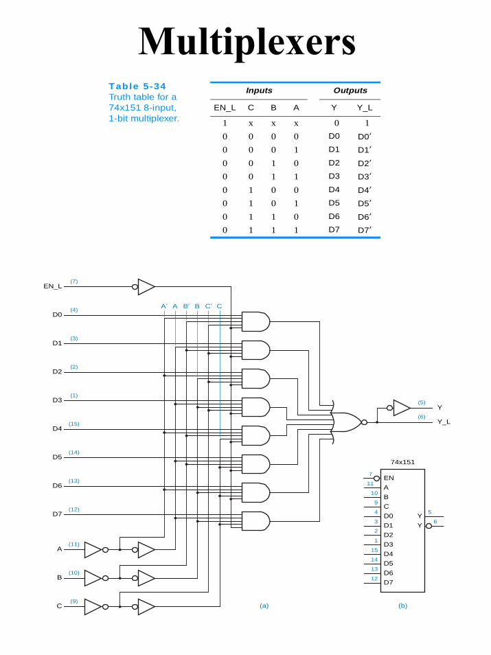
MultiplexersTable 5-34 Truth table for a 74x151 8-input, 1-bit multiplexer.
Inputs Outputs
EN_L C B A Y Y_L
1 x x x 0 1
0 0 0 0 D0 D0′0 0 0 1 D1 D1′0 0 1 0 D2 D2′0 0 1 1 D3 D3′0 1 0 0 D4 D4′0 1 0 1 D5 D5′0 1 1 0 D6 D6′0 1 1 1 D7 D7′
(4)
(3)
(2)
(5)
(6)
(1)
(15)
(14)
(13)
(12)
(11)
(10)
(9)
(7)
(a) (b)
A′ A B′ B C′ CD0
D1
D2
D3
D4
D5
D6
D7
A
B
C
EN_L
Y
Y_L
74x151
D0
D1
D2
D3
D4
D5
D6
D7
EN
4
6
5Y
Y3
2
1
15
14
13
12
A
B
C
11
10
9
7
Multiplexers
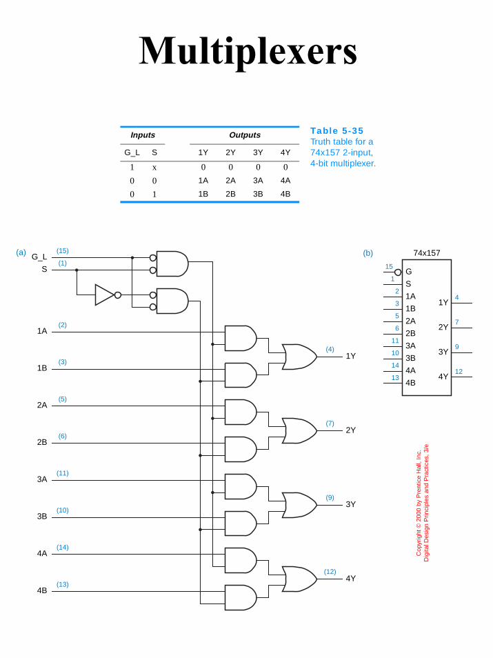
Inputs Outputs Table 5-35 Truth table for a 74x157 2-input, 4-bit multiplexer.
G_L S 1Y 2Y 3Y 4Y
1 x 0 0 0 0
0 0 1A 2A 3A 4A
0 1 1B 2B 3B 4B
(2)
(3)
(5)
(6)
(11)
(10)
(14)
(13)
(1)
(15)(a) (b)
1A
1B
2A
2B
3A
3B
4A
4B
S
G_L 74x157
1A
1B
2A
2B
3A
3B
4A
4B
G
24
1Y
72Y
93Y
124Y
3
5
6
11
10
14
13
S1
15
(4)
(7)
(9)
(12)
1Y
2Y
3Y
4Y
Cop
yrig
ht ©
200
0 by
Pre
ntic
e H
all,
Inc.
Dig
ital D
esig
n P
rinci
ples
and
Pra
ctic
es, 3
/e
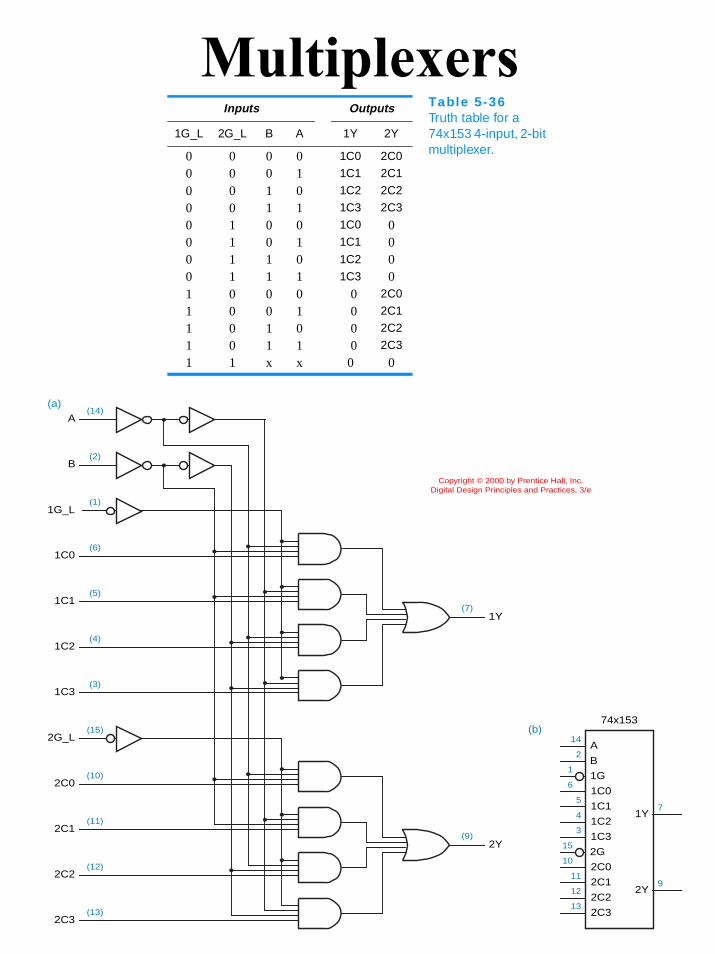
MultiplexersInputs Outputs Table 5-36
Truth table for a 74x153 4-input, 2-bit multiplexer.
1G_L 2G_L B A 1Y 2Y
0 0 0 0 1C0 2C0
0 0 0 1 1C1 2C1
0 0 1 0 1C2 2C2
0 0 1 1 1C3 2C3
0 1 0 0 1C0 00 1 0 1 1C1 00 1 1 0 1C2 00 1 1 1 1C3 01 0 0 0 0 2C0
1 0 0 1 0 2C1
1 0 1 0 0 2C2
1 0 1 1 0 2C3
1 1 x x 0 0
(6)
(5)
(4)
(3)
(14)(a)
(b)
1C0
1C1
1C2
(15)
(1)
2G_L
1C3
A
(2)B
74x153
1G
1C0
1C1
1C2
1C3
2C0
2C1
2C2
2C3
A
1
71Y
92Y
6
5
4
3
15
10
11
12
13
B2
14
2G
(7)1Y
(10)
(11)
(12)
(13)
2C0
1G_L
2C1
2C2
2C3
(9)2Y
Copyright © 2000 by Prentice Hall, Inc.Digital Design Principles and Practices, 3/e
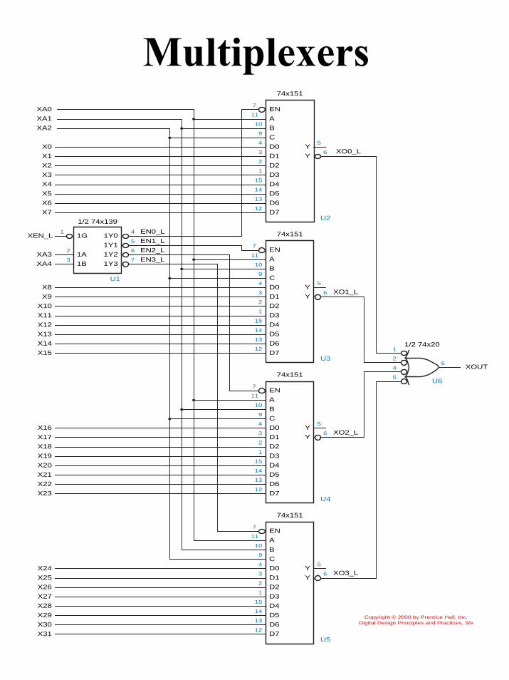
Multiplexers74x151
D0
D1
D2
D3
D4
D5
D6
D7
EN
4
6Y
Y3
2
1
15
14
13
12
A
B
C
11
7
10
9
1/2 74x139
1A
1G
1B
1Y0
1Y1
1Y2
1Y3
1 4
5
6
7
2
3
XEN_L
XA3
XA4
XA0
XA2
XA1
X0
X2
X1
X3
X4
X5
X7
X6
EN3_L
EN2_L
EN1_L
EN0_L 74x151
D0
D1
D2
D3
D4
D5
D6
D7
EN
4
6Y
Y3
2
1
15
14
13
12
A
B
C
11
7
10
9
X10
X12
X11
X13
X14
X15
X9
X8
74x151
D0
D1
D2
D3
D4
D5
D6
D7
EN
4
6Y
Y3
2
1
15
14
13
12
A
B
C
11
7
10
9
74x151
D0
D1
D2
D3
D4
D5
D6
D7
EN
4
6Y
Y3
2
1
15
14
13
12
A
B
C
11
7
10
9
X16
X18
X17
X19
X20
X21
X23
X22
X24
X26
X25
X27
X28
X29
X31
X30
1/2 74x201
2
46
5
XOUT
XO0_L
XO1_L
XO2_L
XO3_L
U1
U5
U4
U3
U2
5
5
5
5
U6
Copyright © 2000 by Prentice Hall, Inc.Digital Design Principles and Practices, 3/e
Demultiplexers
• Digital switch (page 405).• A demultiplexer with n data
outputs requires s = log2 n select lines.
(a)
(b)
SRCA
SRCB
SRCC
SRCZ
SRCA
SRCB
SRCC
SRCZ
BUS
BUS
DSTA
DSTB
DSTC
DSTZ
SRCSEL DSTSEL
multiplexer demultiplexer
MUX DMUX
DSTA
DSTB
DSTC
DSTZ
SRCSEL DSTSEL
Copyright © 2000 by Prentice Hall, Inc.Digital Design Principles and Practices, 3/e
Demultiplexers
1/2 74x139
A
G
B
Y0
Y1
Y2
Y3
(b)
DST0DATA_L
DST1DATA_L
DST2DATA_L
DST3DATA_L
SRCDATA_L
DSTSEL0
DSTSEL1
2-to-4 decoder
A
G
B
Y0
Y1
Y2
Y3
(a)
DST0DATA
DST1DATA
DST2DATA
DST3DATA
SRCDATA
DSTSEL0
DSTSEL1
Copyright © 2000 by Prentice Hall, Inc.Digital Design Principles and Practices, 3/e
Table 5-6Truth table for one-half of a 74x139 dual 2-to-4 decoder.
Inputs Outputs
G_L B A Y3_L Y2_L Y1_L Y0_L
1 x x 1 1 1 10 0 0 1 1 1 00 0 1 1 1 0 10 1 0 1 0 1 10 1 1 0 1 1 1
Exclusive-Or Gates• An exclusive-or (XOR) gate is
a 2 input device whose output is 1 if exactly one of its inputs is 1 (page 410).
• An exclusive-nor (XNOR) or equivalence is just the opposite.
(a)
(b)
Copyright © 2000 by Prentice Hall, Inc.Digital Design Principles and Practices, 3/e
Exclusive-Or Gates
X YX ⊕ Y(XOR)
(X ⊕ Y)′(XNOR)
Table 5-45 Truth table for XOR and XNOR functions.
0 0 0 1
0 1 1 0
1 0 1 0
1 1 0 1
X
Y
X
Y
F
F
= X ⊕ Y
(a)
(b)
= X ⊕ Y
Copyright © 2000 by Prentice Hall, Inc.Digital Design Principles and Practices, 3/e
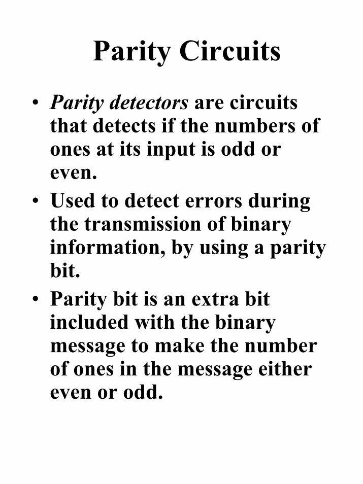
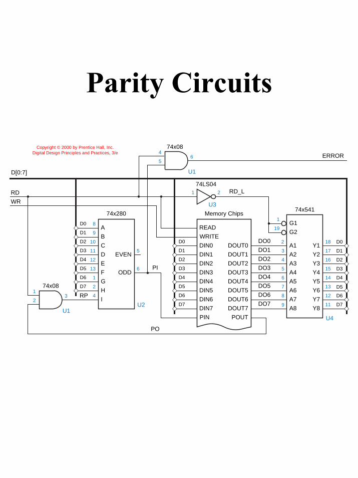
Parity Circuits
• Parity detectors are circuits that detects if the numbers of ones at its input is odd or even.
• Used to detect errors during the transmission of binary information, by using a parity bit.
• Parity bit is an extra bit included with the binary message to make the number of ones in the message either even or odd.
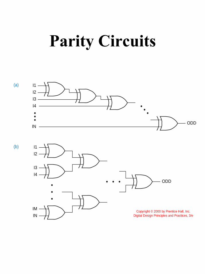
Parity Circuits
I1
I2
I3
I4
I1
I2
I3
I4
IN
IM
IN
ODD
ODD
(a)
(b)
Copyright © 2000 by Prentice Hall, Inc.Digital Design Principles and Practices, 3/e
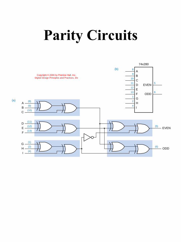
Parity Circuits
(a)
(b)
A
B
C
(8)
(9)
(10)
D
E
F
(11)
(12) (5)
(6)
(13)
G
H
I
(1)
(2)
(4)
EVEN
ODD
74x280
D
E
F
G
H
I
12
5EVEN
ODD13
1
2
4
A
B
C
9
8
10
11
6
Copyright © 2000 by Prentice Hall, Inc.Digital Design Principles and Practices, 3/e
Parity Circuits
74x280
D
E
F
G
H
I
12
5
2
EVEN
ODD13
1
2
4
A
B
C
9
8
1
10
11
6
D0
D1
D2
D3
D4
D5
D6
D7
U2
U4U1
U1D[0:7]
RP1
23
4
56
Memory Chips
DIN3
DIN4
DIN5
DIN6
DIN7
PIN
DIN0
READ
WRITE
DIN1
DIN2
DOUT3
DOUT4
DOUT5
DOUT6
DOUT7
POUT
DOUT0
DOUT1
DOUT2
D0
D1
D2
D3
D4
D5
D6
D7
D4
D5
D0
D1
D2
D3
D6
D7
74x541
G2
G1
Y1
Y2
Y3
1
19
15
14
16
17
18
13
A1
A2
A3
A4
A5
A6
A7
A8
Y4
Y5
Y6
Y7
Y8
2
12
11
3
4
5
6
7
8
9
DO0
DO1
DO2
DO3
DO4
DO5
DO6
DO7
74LS04
U3
74x08
74x08
ERROR
RD_L
PI
PO
RD
WR
Copyright © 2000 by Prentice Hall, Inc.Digital Design Principles and Practices, 3/e
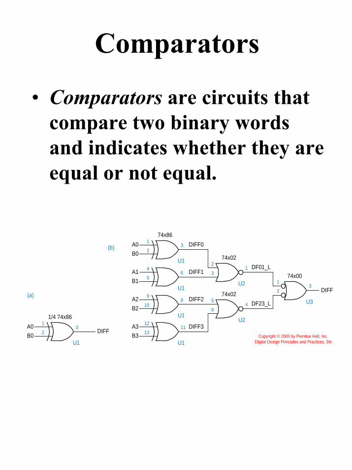
Comparators
• Comparators are circuits that compare two binary words and indicates whether they are equal or not equal.
1/4 74x86
A0
B0
74x86
74x02
74x02
74x00
A0
B0
A1
B1
A2
B2
A3
B3DIFF
DIFF(a)
(b)
1
2
12
1311
9
108
4
56
1
23
3
1
23
2
31
5
64
U1 U1
U1
U1
U1
U2
U3
U2
DIFF0
DIFF1
DIFF2
DIFF3
DF01_L
DF23_L
Copyright © 2000 by Prentice Hall, Inc.Digital Design Principles and Practices, 3/e
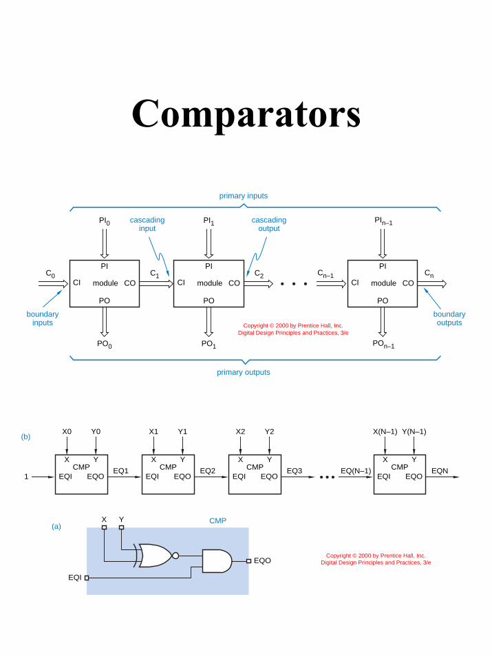
Comparators
primary inputs
primary outputs
moduleCI CO
PIC2C1C0 Cn–1 Cn
POn–1
PIn–1
PO
moduleCI CO
PI
PO
moduleCI CO
PI
PO
PI1
PO1PO0
PI0 cascadinginput
cascadingoutput
boundaryinputs
boundaryoutputsCopyright © 2000 by Prentice Hall, Inc.
Digital Design Principles and Practices, 3/e
XCMP
Y
X0 Y0
EQI EQO
XCMP
Y
EQI EQO
XCMP
Y
EQI EQO
XCMP
Y
EQI EQOEQ1
X1 Y1
EQ2
X2 Y2 X(N–1) Y(N–1)
EQ3 EQNEQ(N–1)
(b)
1
EQO
EQI
X Y(a)
CMP
Copyright © 2000 by Prentice Hall, Inc.Digital Design Principles and Practices, 3/e
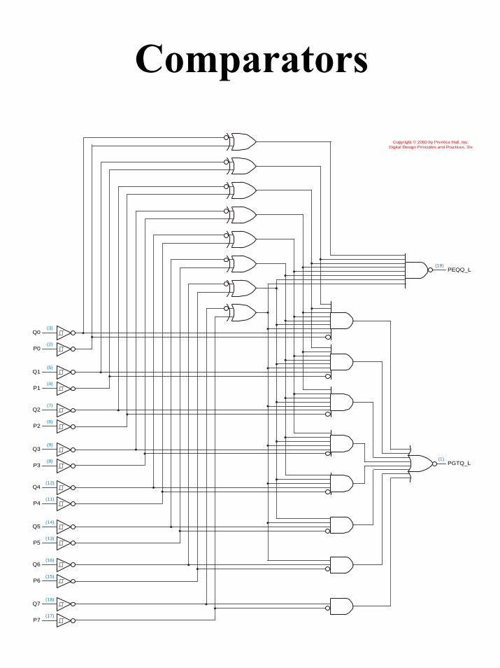
Comparators
Q0(3)
P0(2)
Q2(7)
P2
P4
(6)
Q4(12)
(11)
Q6(16)
P6(15)
Q1(5)
P1(4)
Q3(9)
P3(8)
Q5(14)
P5(13)
Q7(18)
P7(17)
PEQQ_L
PGTQ_L
(19)
(1)
Copyright © 2000 by Prentice Hall, Inc.Digital Design Principles and Practices, 3/e
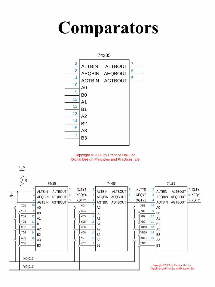
Comparators74x85
9
5
ALTBOUT
AEQBOUT
AGTBOUT
12
11
13
14
AEQBIN
ALTBIN
AGTBIN
A0
B0
A1
B1
A2
B2
A3
B3
3
2
4
10
15
1
6
7
Copyright © 2000 by Prentice Hall, Inc.Digital Design Principles and Practices, 3/e
74x85
ALTBOUT
AEQBOUT
AGTBOUT
AEQBIN
ALTBIN
AGTBIN
A0
B0
A1
B1
A2
B2
A3
B3YD3
YD2
YD1
YD0
XD3
XD2
XD1
XD0
XLTY4
XEQY4
XGTY4
74x85
ALTBOUT
AEQBOUT
AGTBOUT
AEQBIN
ALTBIN
AGTBIN
A0
B0
A1
B1
A2
B2
A3
B3YD7
YD6
YD5
YD4
XD7
XD6
XD5
XD4
XLTY8
XEQY8
XGTY8
74x85
ALTBOUT
AEQBOUT
AGTBOUT
AEQBIN
ALTBIN
AGTBIN
9
12
11
13
14
3
2
4
10
15
1
6
7
9
12
11
13
14
3
2
4
10
15
1
6
7
9
5 5 5
12
11
13
14
3
2
4
10
15
1
6
7
A0
B0
A1
B1
A2
B2
A3
B3YD11
YD10
YD9
YD8
XD11
XD10
XD9
XD8
XLTY
XEQY
XGTY
XD[011]
YD[011]
+5 V
R
Copyright © 2000 by Prentice Hall, Inc.Digital Design Principles and Practices, 3/e
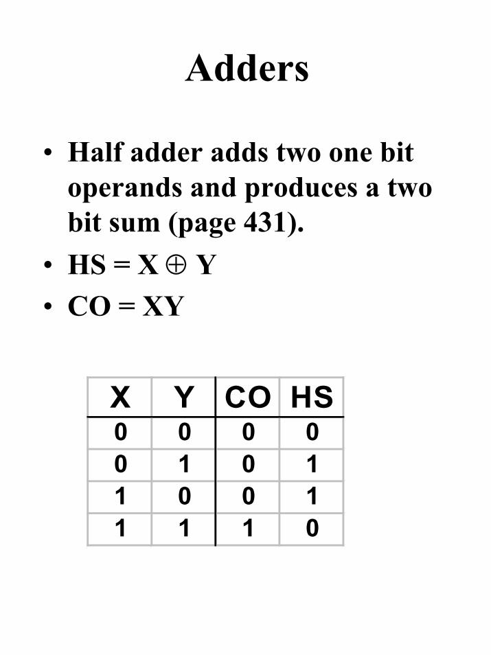
Adders
• Half adder adds two one bit operands and produces a two bit sum (page 431).
• HS = X ⊕ Y• CO = XY
X Y CO HS0 0 0 00 1 0 11 0 0 11 1 1 0
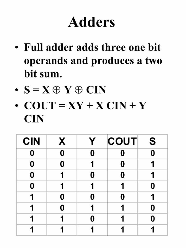
Adders• Full adder adds three one bit
operands and produces a two bit sum.
• S = X ⊕ Y ⊕ CIN• COUT = XY + X CIN + Y
CIN
CIN X Y COUT S0 0 0 0 00 0 1 0 10 1 0 0 10 1 1 1 01 0 0 0 11 0 1 1 01 1 0 1 01 1 1 1 1
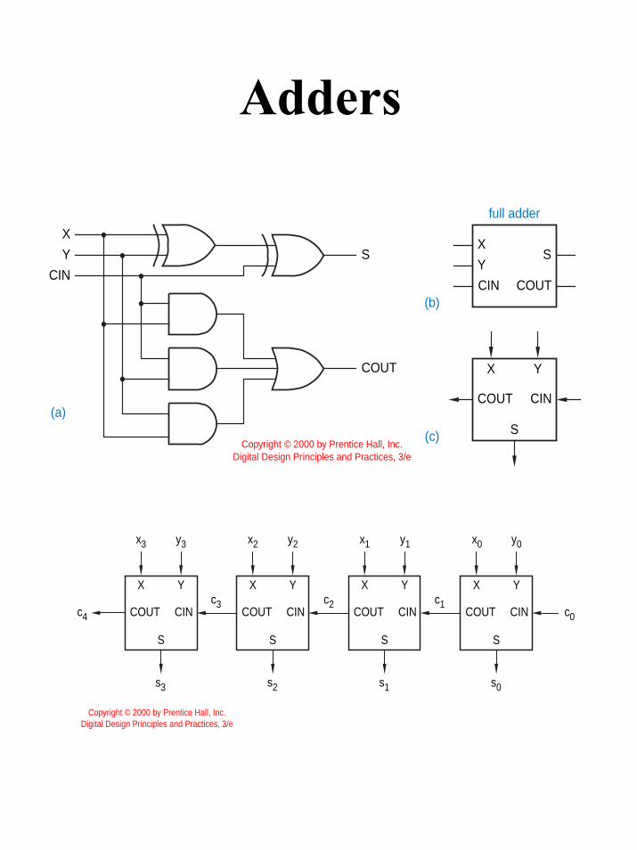
Adders
(a)
(b)
X
Y
CIN
S
COUT
X
Y
CIN
S
COUT
full adder
(c)
COUT CIN
X
S
Y
Copyright © 2000 by Prentice Hall, Inc.Digital Design Principles and Practices, 3/e
SSS
COUT CIN
X
S
Y
COUT CIN
X Y
COUT CIN
X Y
COUT CIN
X Y
x2 y2 x1 y1 x0 y0
c3c4
c2 c1
x3 y3
c0
s2 s1 s0s3
Copyright © 2000 by Prentice Hall, Inc.Digital Design Principles and Practices, 3/e
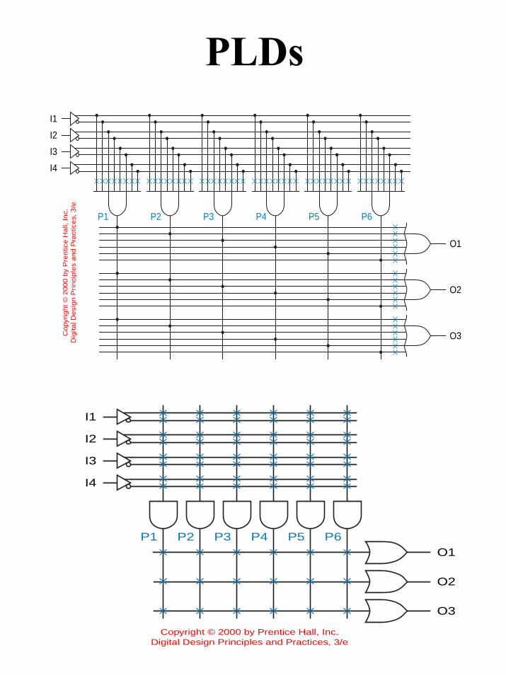
PLDs
I2
I3
I1
I4
P1 P2 P3 P4
O2
O3
O1
P5 P6
Copyr
ight ©
2000 b
y P
rentic
e H
all,
Inc.
Dig
ital D
esi
gn P
rinci
ple
s and P
ract
ices,
3/e
I2
I3
I1
I4
P1 P2 P3 P4 P5 P6
O3
O2
O1
Copyright © 2000 by Prentice Hall, Inc.Digital Design Principles and Practices, 3/e
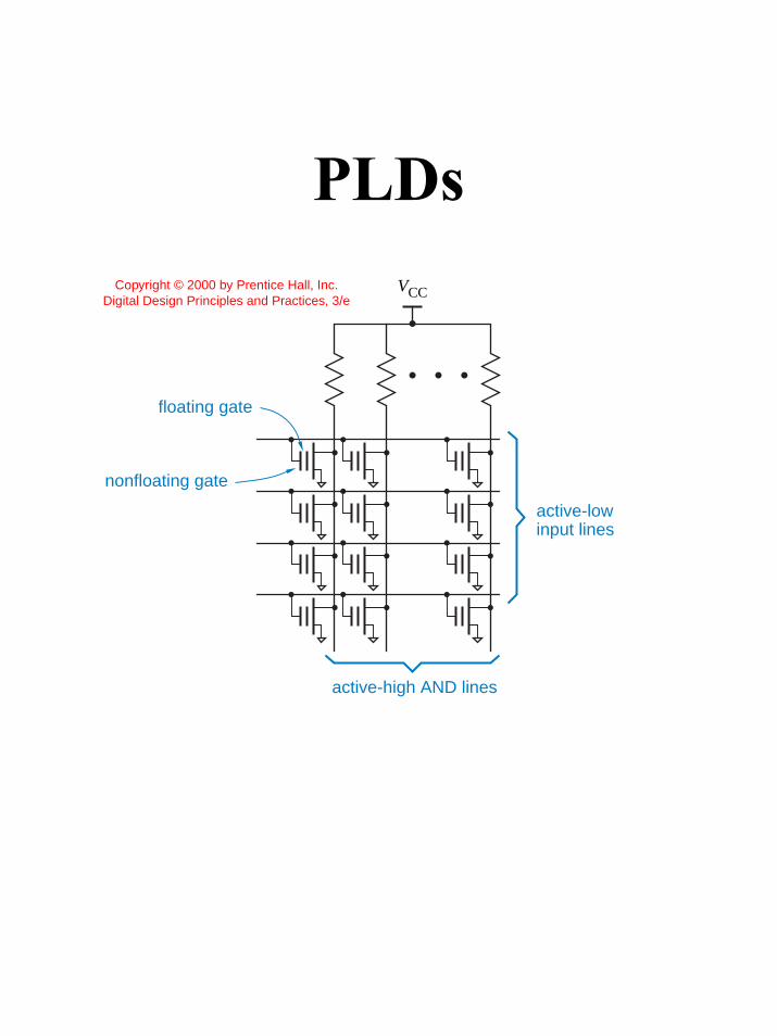
PLDsVCC
floating gate
nonfloating gate
active-lowinput lines
active-high AND lines
Copyright © 2000 by Prentice Hall, Inc.Digital Design Principles and Practices, 3/e
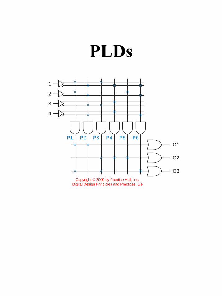
PLDs
I2
I3
I1
I4
P1 P2 P3 P4 P5 P6
O3
O2
O1
Copyright © 2000 by Prentice Hall, Inc.Digital Design Principles and Practices, 3/e
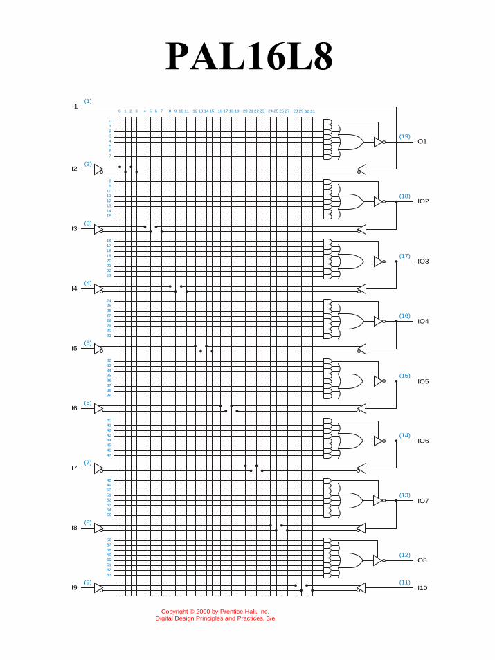
PAL16L830 31
(2)
(19)
(18)
(17)
(16)
(15)
(14)
(13)
(12)
(11)
0 1 2 3 4 5 6 7 8 9 10 11 12 13 14 15 16 17 18 19 20 21 22 23 24 25 26 27 28 29
01234567
89
101112131415
1617181920212223
2425262728293031
3233343536373839
4041424344454647
4849505152535455
5657585960616263
(1)
(3)
(4)
(5)
(6)
(7)
(8)
(9)
I1
I2
I3
I4
I5
I6
I7
I8
I9
O1
IO2
IO3
IO4
IO5
IO6
IO7
O8
I10
Copyright © 2000 by Prentice Hall, Inc.Digital Design Principles and Practices, 3/e
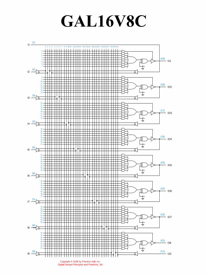
GAL16V8C30 31
(2)
(19)
(18)
(17)
(16)
(15)
(14)
(13)
(12)
(11)
0 1 2 3 4 5 6 7 8 9 10 11 12 13 14 15 16 17 18 19 20 21 22 23 24 25 26 27 28 29
01234567
89
101112131415
1617181920212223
2425262728293031
3233343536373839
4041424344454647
4849505152535455
5657585960616263
(1)
(3)
(4)
(5)
(6)
(7)
(8)
(9)
I1
I2
I3
I4
I5
I6
I7
I8
I9
O1
IO2
IO3
IO4
IO5
IO6
IO7
O8
I10
Copyright © 2000 by Prentice Hall, Inc.Digital Design Principles and Practices, 3/e


![[MS-IEDOCO]: Internet Explorer Standards Support Documentation … · 2018. 11. 27. · Internet Explorer Standards Support Documentation Overview Intellectual Property Rights Notice](https://img.pdfslide.us/doc/110x75/5ff81edc9d58a113b270fb91/ms-iedoco-internet-explorer-standards-support-documentation-2018-11-27-internet.jpg)