Embed Size (px)
Citation preview

MRF6S9125NR1 MRF6S9125NBR1
1RF Device DataFreescale Semiconductor
RF Power Field Effect TransistorsN-Channel Enhancement-Mode Lateral MOSFETs
Designed for broadband commercial and industrial applications withfrequencies up to 1000 MHz. The high gain and broadband performance ofthese devices make them ideal for large -signal, common-source amplifierapplications in 28 volt base station equipment.
N-CDMA Application• Typical Single-Carrier N-CDMA Performance: VDD = 28 Volts, IDQ =
950 mA, Pout = 27 Watt Avg., Full Frequency Band (865-960 MHz), IS-95CDMA (Pilot, Sync, Paging, Traffic Codes 8 Through 13) Channel Bandwidth = 1.2288 MHz. PAR = 9.8 dB @ 0.01% Probability on CCDF.
Power Gain � 20.2 dBDrain Efficiency � 31% ACPR @ 750 kHz Offset = -47.1 dBc in 30 kHz Bandwidth
GSM EDGE Application
• Typical GSM EDGE Performance: VDD = 28 Volts, IDQ = 700 mA, Pout = 60 Watts Avg., Full Frequency Band (865-960 MHz or 921-960 MHz)
Power Gain � 20 dBDrain Efficiency � 40%Spectral Regrowth @ 400 kHz Offset = -63 dBcSpectral Regrowth @ 600 kHz Offset = -78 dBcEVM � 1.8% rms
GSM Application
• Typical GSM Performance: VDD = 28 Volts, IDQ = 700 mA, Pout = 125 Watts, Full Frequency Band (921-960 MHz)
Power Gain � 19 dB Drain Efficiency � 62%
• Capable of Handling 10:1 VSWR, @ 28 Vdc, 880 MHz, 125 Watts CW Output Power
Features• Characterized with Series Equivalent Large-Signal Impedance Parameters
• Internally Matched for Ease of Use• Qualified Up to a Maximum of 32 VDD Operation• Integrated ESD Protection• 200°C Capable Plastic Package• N Suffix Indicates Lead-Free Terminations. RoHS Compliant.• In Tape and Reel. R1 Suffix = 500 Units per 44 mm, 13 inch Reel.
Table 1. Maximum Ratings
Rating Symbol Value Unit
Drain-Source Voltage VDSS -0.5, +68 Vdc
Gate-Source Voltage VGS -0.5, +12 Vdc
Total Device Dissipation @ TC = 25°CDerate above 25°C
PD 3982.3
WW/°C
Storage Temperature Range Tstg - 65 to +150 °C
Operating Junction Temperature TJ 200 °C
Document Number: MRF6S9125NRev. 4, 5/2006
Freescale SemiconductorTechnical Data
MRF6S9125NR1MRF6S9125NBR1
865-960 MHz, 27 W AVG., 28 VSINGLE N-CDMA, GSM EDGE
LATERAL N-CHANNELRF POWER MOSFETs
CASE 1486-03, STYLE 1TO-270 WB-4
PLASTICMRF6S9125NR1
CASE 1484-04, STYLE 1TO-272 WB-4
PLASTICMRF6S9125NBR1
© Freescale Semiconductor, Inc., 2006. All rights reserved.
Downloaded from Elcodis.com electronic components distributor

2RF Device Data
Freescale Semiconductor
MRF6S9125NR1 MRF6S9125NBR1
Table 2. Thermal Characteristics
Characteristic Symbol Value (1,2) Unit
Thermal Resistance, Junction to CaseCase Temperature 80°C, 125 W CWCase Temperature 76°C, 27 W CW
RθJC0.440.45
°C/W
Table 3. ESD Protection Characteristics
Test Methodology Class
Human Body Model (per JESD22-A114) 1B (Minimum)
Machine Model (per EIA/JESD22-A115) C (Minimum)
Charge Device Model (per JESD22-C101) IV (Minimum)
Table 4. Moisture Sensitivity Level
Test Methodology Rating Package Peak Temperature Unit
Per JESD 22-A113, IPC/JEDEC J-STD-020 3 260 °C
Table 5. Electrical Characteristics (TC = 25°C unless otherwise noted)
Characteristic Symbol Min Typ Max Unit
Off Characteristics
Zero Gate Voltage Drain Leakage Current(VDS = 68 Vdc, VGS = 0 Vdc)
IDSS � � 10 μAdc
Zero Gate Voltage Drain Leakage Current(VDS = 28 Vdc, VGS = 0 Vdc)
IDSS � � 1 μAdc
Gate-Source Leakage Current(VGS = 5 Vdc, VDS = 0 Vdc)
IGSS � � 1 μAdc
On Characteristics
Gate Threshold Voltage(VDS = 10 Vdc, ID = 400 μAdc)
VGS(th) 1 2.1 3 Vdc
Gate Quiescent Voltage(VDS = 28 Vdc, ID = 950 mAdc)
VGS(Q) 2 2.89 4 Vdc
Drain-Source On-Voltage(VGS = 10 Vdc, ID = 2.74 Adc)
VDS(on) 0.05 0.23 0.3 Vdc
Forward Transconductance(VDS = 10 Vdc, ID = 8 Adc)
gfs � 6 � S
Dynamic Characteristics (3)
Reverse Transfer Capacitance(VDS = 28 Vdc ± 30 mV(rms)ac @ 1 MHz, VGS = 0 Vdc)
Crss � 2 � pF
Output Capacitance(VDS = 28 Vdc ± 30 mV(rms)ac @ 1 MHz, VGS = 0 Vdc)
Coss � 60 � pF
Functional Tests (In Freescale Test Fixture, 50 ohm system) VDD = 28 Vdc, IDQ = 950 mA, Pout = 27 W Avg. N-CDMA, f = 880 MHz,Single-Carrier N-CDMA, 1.2288 MHz Channel Bandwidth Carrier. ACPR measured in 30 kHz Channel Bandwidth @ ±750 kHz Offset. PAR= 9.8 dB @ 0.01% Probability on CCDF.
Power Gain Gps 19 20.2 24 dB
Drain Efficiency ηD 29 31 � %
Adjacent Channel Power Ratio ACPR � -47.1 -45 dBc
Input Return Loss IRL � -16 -9 dB
1. MTTF calculator available at http://www.freescale.com/rf. Select Tools/Software/Application Software/Calculators to access the MTTF calculators by product.
2. Refer to AN1955, Thermal Measurement Methodology of RF Power Amplifiers. Go to http://www.freescale.com/rf. Select Documentation/Application Notes - AN1955.
3. Part is internally input matched.
(continued)
Downloaded from Elcodis.com electronic components distributor
MRF6S9125NR1 MRF6S9125NBR1
3RF Device DataFreescale Semiconductor
Table 5. Electrical Characteristics (TC = 25°C unless otherwise noted) (continued)
Characteristic Symbol Min Typ Max Unit
Typical GSM EDGE Performances (In Freescale GSM EDGE Test Fixture, 50 οhm system) VDD = 28 Vdc, IDQ = 700 mA, Pout = 60 W Avg., 921-960 MHz, EDGE Modulation
Power Gain Gps � 20 � dB
Drain Efficiency ηD � 40 � %
Error Vector Magnitude EVM � 1.8 � % rms
Spectral Regrowth at 400 kHz Offset SR1 � -63 � dBc
Spectral Regrowth at 600 kHz Offset SR2 � -78 � dBc
Typical CW Performances (In Freescale GSM Test Fixture, 50 οhm system) VDD = 28 Vdc, IDQ = 700 mA, Pout = 125 W, 921-960 MHz
Power Gain Gps � 19 � dB
Drain Efficiency ηD � 62 � %
Input Return Loss IRL � -12 � dB
Pout @ 1 dB Compression Point, CW(f = 880 MHz)
P1dB � 125 � W
Downloaded from Elcodis.com electronic components distributor

4RF Device Data
Freescale Semiconductor
MRF6S9125NR1 MRF6S9125NBR1
Figure 1. MRF6S9125NR1(NBR1) Test Circuit Schematic
Z10 0.057″ x 0.620″ MicrostripZ11 0.119″ x 0.620″ MicrostripZ12 0.450″ x 0.220″ MicrostripZ13 0.061″ x 0.220″ MicrostripZ14 0.078″ x 0.220″ MicrostripZ15 0.692″ x 0.080″ MicrostripZ16 0.368″ x 0.080″ MicrostripPCB Arlon GX-0300-55-22, 0.030″, εr = 2.55
Z1, Z17 0.200″ x 0.080″ MicrostripZ2 1.060″ x 0.080″ MicrostripZ3 0.382″ x 0.220″ MicrostripZ4 0.108″ x 0.220″ MicrostripZ5 0.200″ x 0.420″ x 0.620″ TaperZ6 0.028″ x 0.620″ MicrostripZ7 0.236″ x 0.620″ MicrostripZ8 0.050″ x 0.620″ MicrostripZ9 0.238″ x 0.620″ Microstrip
R2
VBIAS
VSUPPLY
RF
OUTPUTRF
INPUT
DUTC3
L1
Z1
C2
Z2 Z3
C1
Z4 Z5 Z6 Z7
C4
Z8
Z9
R1
L2C10 C6
C11
C18 C20 C21 C22
C9
Z10 Z11 Z12 Z14 Z15
+
+ + +
C8
+
C7
+
C5
C12 C13
Z13
C14 C15 C16
Z16
C17
Z17
C23C19
Table 6. MRF6S9125NR1(NBR1) Test Circuit Component Designations and ValuesPart Description Part Number Manufacturer
C1 20 pF Chip Capacitor 600B200FT250XT ATC
C2 6.2 pF Chip Capacitor 600B6R2BT250XT ATC
C3, C15 0.8-8.0 pF Variable Capacitors, Gigatrim 27291SL Johanson
C4, C5 11 pF Chip Capacitors 600B110FT250XT ATC
C6, C18, C19 0.56 μF, 50 V Chip Capacitors C1825C564J5RAC Kemet
C7, C8 47 μF, 16 V Tantalum Capacitors 593D476X9016D2T Vishay
C9, C23 47 pF Chip Capacitors 700B470FW500XT ATC
C10 100 μF, 50 V Electrolytic Capacitor 515D107M050BB6A Vishay
C11, C12 12 pF Chip Capacitors 600B120FT250XT ATC
C13, C14 5.1 pF Chip Capacitors 600B5R1BT250XT ATC
C16 0.3 pF Chip Capacitor 700B0R3BW500XT ATC
C17 39 pF Chip Capacitor 700B390FW500XT ATC
C20, C21 22 μF, 35 V Tantalum Capacitors T491X226K035AS Kemet
C22 470 μF, 63 V Electrolytic Capacitor SME63V471M12X25LL United Chemi-Con
L1 7.15 nH Inductor 1606-7J CoilCraft
L2 8.0 nH Inductor A03T CoilCraft
R1 15 Ω, 1/4 W Chip Resistor (1210)
R2 560 kΩ, 1/8 W Resistor (1206)
Downloaded from Elcodis.com electronic components distributor

MRF6S9125NR1 MRF6S9125NBR1
5RF Device DataFreescale Semiconductor
Figure 2. MRF6S9125NR1(NBR1) Test Circuit Component Layout
CU
T O
UT
AR
EA
C9
R2
C10
VGG VDD
C8 C7
C1
C2
C3
C5
L1
C4
C6
C12
C13 C15 C16
C17C14
L2
C11 C23C18
C19
C20 C21 C22
900 MHz
TO272 WB
Rev. 0
R1
Downloaded from Elcodis.com electronic components distributor

6RF Device Data
Freescale Semiconductor
MRF6S9125NR1 MRF6S9125NBR1
TYPICAL CHARACTERISTICS
Gps
, PO
WE
R G
AIN
(dB
)
IRL,
IN
PU
T R
ET
UR
N L
OS
S (
dB)
AC
PR
(dB
c), A
LT1
(dB
c)
−25
−20
910850
IRL
Gps
ACPR
f, FREQUENCY (MHz)
Figure 3. Single-Carrier N-CDMA Broadband Performance @ Pout = 27 Watts Avg.
890880870860
18.5
20.5
20.3
−70
34
32
30
−40
−50
−60
η D,
DR
AIN
EF
FIC
IEN
CY
(%
)
20
19.8
19.5
19.3
19
−30
900
ALT1
−15
−10
−5
VDD = 28 Vdc, Pout = 27 W (Avg.)IDQ = 950 mA, N−CDMA IS−95 PilotSync, Paging, Traffic Codes 8 Through 13
Gps
, PO
WE
R G
AIN
(dB
)
IRL,
IN
PU
T R
ET
UR
N L
OS
S (
dB)
AC
PR
(dB
c), A
LT1
(dB
c)
−25
−20
910850
IRL
Gps
ACPR
f, FREQUENCY (MHz)
Figure 4. Single-Carrier N-CDMA Broadband Performance @ Pout = 62.5 Watts Avg.
900890880870860
18
19.6
19.4
−70
52
48
44
−40
−50
−60η D
, D
RA
IN
EF
FIC
IEN
CY
(%
)
19.2
19
18.8
18.6
18.4
−30
−15
−10
−5
VDD = 28 Vdc, Pout = 62.5 W (Avg.)
IDQ = 950 mA, N−CDMA IS−95 Pilot
Sync, Paging, Traffic Codes 8 Through 13
Figure 5. Two-Tone Power Gain versusOutput Power
10016
22IDQ = 1475 mA
Pout, OUTPUT POWER (WATTS) PEP
20
18
10
Gps
, PO
WE
R G
AIN
(dB
)
21
19
1187 mA
950 mA
1 300
VDD = 28 Vdc, f1 = 880 MHz, f2 = 880.1 MHz
Two−Tone Measurements
Figure 6. Third Order Intermodulation Distortionversus Output Power
−30
−10
1
Pout, OUTPUT POWER (WATTS) PEP
10
−20
100−60
−40
INT
ER
MO
DU
LAT
ION
DIS
TO
RT
ION
(dB
c)
IMD
, T
HIR
D O
RD
ER
−50
18.2
40
17
712 mA
475 mA
18.8
28
ηD
ηD
ALT1
300
IDQ = 1425 mA
1187 mA 950 mA
712 mA
475 mA
VDD = 28 Vdc
f1 = 880 MHz, f2 = 880.1 MHz
Two−Tone Measurements
Downloaded from Elcodis.com electronic components distributor

MRF6S9125NR1 MRF6S9125NBR1
7RF Device DataFreescale Semiconductor
TYPICAL CHARACTERISTICS
Figure 7. Intermodulation Distortion Productsversus Output Power
10
−70
−10
7th Order
Pout, OUTPUT POWER (WATTS) PEP
5th Order
3rd Order
−20
−30
−40
1 300
IMD
, IN
TE
RM
OD
ULA
TIO
N D
IST
OR
TIO
N (
dBc)
−50
−60
100
Figure 8. Intermodulation Distortion Productsversus Tone Spacing
10
−60
−10
0.1
7th Order
TWO−TONE SPACING (MHz)
VDD = 28 Vdc, Pout = 125 W (PEP)
IDQ = 950 mA, Two−Tone Measurements
(f1 + f2)/2 = Center Frequency of 880 MHz
5th Order
−20
−30
−40
−50
1 100
IMD
, IN
TE
RM
OD
ULA
TIO
N D
IST
OR
TIO
N (
dBc)
Figure 9. Pulse CW Output Power versusInput Power
36
56
29
P3dB = 52.4 dBm (172.5 W)
Pin, INPUT POWER (dBm)
VDD = 28 Vdc, IDQ = 950 mA
Pulsed CW, 8 μsec(on), 1 msec(off)
f = 880 MHz
54
52
50
48
30 3231 3433 35
Actual
Ideal55
53
49
51
28
Pou
t, O
UT
PU
T P
OW
ER
(dB
m)
Figure 10. Single-Carrier N-CDMA ACPR, ALT1, PowerGain and Drain Efficiency versus Output Power
0 −80
Pout, OUTPUT POWER (WATTS) AVG.
50 −30
40 −40
30 −50
20 −60
10
0.1 10
−70
ALT1ηD
Gps
TC = −30�C
85�C
ACPR
η D, D
RA
IN E
FF
ICIE
NC
Y (
%),
Gps
, PO
WE
R G
AIN
(dB
)
VDD = 28 Vdc, IDQ = 950 mA
f = 880 MHz, N−CDMA IS−95 (Pilot
Sync, Paging, Traffic Codes 8
Through 13)
ALT
1, C
HA
NN
EL
PO
WE
R (
dBc)
AC
PR
, A
DJA
CE
NT
CH
AN
NE
L P
OW
ER
RA
TIO
(dB
c)
3rd Order
−30�C
P1dB = 51.5 dBm (139.3 W)
1 100 200
25�C
85�C
25�C
−30�C25�C
25�C
85�C
VDD = 28 Vdc, IDQ = 950 mA
f1 = 880 MHz, f2 = 880.1 MHz
Two−Tone Measurements
Downloaded from Elcodis.com electronic components distributor

8RF Device Data
Freescale Semiconductor
MRF6S9125NR1 MRF6S9125NBR1
TYPICAL CHARACTERISTICS
100
22
1
0
70
Pout, OUTPUT POWER (WATTS) CW
Figure 11. Power Gain and Drain Efficiencyversus CW Output Power
VDD = 28 Vdc
IDQ = 950 mA
f = 880 MHz
TC = −30�C−30�C
85�C
10
21
20
18
16
60
50
40
30
20
η D, D
RA
IN E
FF
ICIE
NC
Y (
%)
Gps
ηD
Gps
, PO
WE
R G
AIN
(dB
)
Figure 12. Power Gain versus Output Power
Pout, OUTPUT POWER (WATTS) CW
VDD = 12 V
16 V
Gps
, PO
WE
R G
AIN
(dB
)
25016
21
0
17
19
18
20
IDQ = 950 mA
f = 880 MHz
19
17
15
10
25�C
50 100 200
20 V
24 V
28 V
32 V
200
85�C
25�C
150
210
109
TJ, JUNCTION TEMPERATURE (°C)
This above graph displays calculated MTTF in hours x ampere2
drain current. Life tests at elevated temperatures have correlated to
better than ±10% of the theoretical prediction for metal failure. Divide
MTTF factor by ID2 for MTTF in a particular application.
108
107
MT
TF
FA
CT
OR
(H
OU
RS
X A
MP
S2 )
90 110 130 150 170 190
Figure 13. MTTF Factor versus Junction Temperature
100 120 140 160 180 200
Downloaded from Elcodis.com electronic components distributor

MRF6S9125NR1 MRF6S9125NBR1
9RF Device DataFreescale Semiconductor
N-CDMA TEST SIGNAL
10
0.0001
100
0
PEAK −TO−AVERAGE (dB)
Figure 14. Single-Carrier CCDF N-CDMA
10
1
0.1
0.01
0.001
2 4 6 8
IS−95 CDMA (Pilot, Sync, Paging, Traffic Codes 8
Through 13) 1.2288 MHz Channel Bandwidth
Carriers. ACPR Measured in 30 kHz Bandwidth @
±750 kHz Offset. ALT1 Measured in 30 kHz
Bandwidth @ ±1.98 MHz Offset. PAR = 9.8 dB @
0.01% Probability on CCDF.
PR
OB
AB
ILIT
Y (
%)
.................
... ....... ......... ...... .................................
.
.......
...
......... ..... .............. ..... ... ... ..... . .... ..... .. ...
.
............ ..........................................
............... ........... ....... .........................
....... .... ......... ........... ... ... ... .......................
....................... .... .. .................... ..... .... ................... . ... ..... .... .... .. ....... ......... .. ... ... .. . ....... ... .......... .... .. ..
... .................. .. ... .
.............. .... ................................................................................. ... .... .....
... .............. ... ... ... ...................... .. ..... ........................ ....... .............. .
.............................. ...........................................................
.... ....... ............................ ....... ......................... ......... ................... .... .........
.....
......
....
..
..
..
....
....
..... ... ... .............. ...... ... ... .... .. ... .......... .. .... ... ................ ...... .....
.........................
..
..............
.
............
.
. ................. ..... . ...
........
...................................................
...
−60
−110
−10
(dB
)
−20
−30
−40
−50
−70
−80
−90
−100
+ACPR in 30 kHzIntegrated BW
1.2288 MHzChannel BW
2.90.7 2.21.50−0.7−1.5−2.2−2.9−3.6 3.6
f, FREQUENCY (MHz)
Figure 15. Single-Carrier N-CDMA Spectrum
−ACPR in 30 kHzIntegrated BW
−ALT1 in 30 kHzIntegrated BW
+ALT1 in 30 kHzIntegrated BW
Downloaded from Elcodis.com electronic components distributor
10RF Device Data
Freescale Semiconductor
MRF6S9125NR1 MRF6S9125NBR1
f = 860 MHz
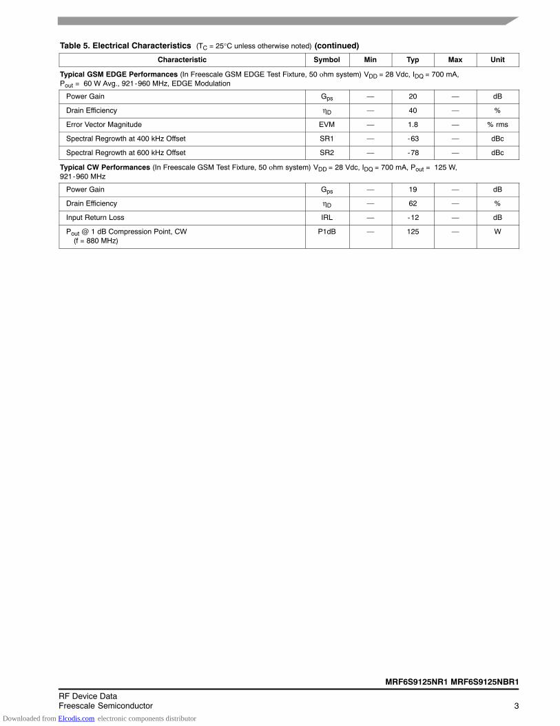
Figure 16. Series Equivalent Source and Load Impedance
fMHz
ZsourceΩ
ZloadΩ
860
865
870
1.48 - j0.14
1.66 - j0.02
1.56 - j0.09
0.62 - j2.13
0.64 - j2.31
0.62 - j2.45
VDD = 28 Vdc, IDQ = 950 mA, Pout = 27 W Avg.
875
880 1.74 + j0.11
1.73 + j0.040.59 - j2.43
0.57 - j2.42
Zsource = Test circuit impedance as measured from gate to ground.
Zload = Test circuit impedance as measured from drain to ground.
Zsource
Zload
Input
Matching
Network
Device
Under
Test
Output
Matching
Network
885
890
895
1.68 + j0.19
1.52 + j0.33
1.61 + j0.25
0.54 - j2.36
0.57 - j2.18
0.58 - j1.94
900 1.48 + j0.370.59 - j1.86
Zo = 5 Ω
f = 900 MHzZsource
f = 900 MHz
f = 860 MHz
Zload
Downloaded from Elcodis.com electronic components distributor

MRF6S9125NR1 MRF6S9125NBR1
11RF Device DataFreescale Semiconductor
EDGE CHARACTERIZATION
Figure 17. MRF6S9125NR1(NBR1) Test Circuit Schematic
Z9 0.620″ x 0.100″ x 0.420″ TaperZ10 0.420″ x 0.100″ x 0.220″ TaperZ11 0.325″ x 0.220″ MicrostripZ12 0.040″ x 0.220″ MicrostripZ13 0.475″ x 0.080″ MicrostripZ14 0.400″ x 0.080″ MicrostripPCB Arlon GX-0300-55-22, 0.030″, εr = 2.55
Z1, Z15 0.150″ x 0.080″ MicrostripZ2 1.050″ x 0.080″ MicrostripZ3 0.330″ x 0.220″ MicrostripZ4 0.220″ x 0.100″ x 0.420″ TaperZ5 0.420″ x 0.100″ x 0.620″ TaperZ6 0.200″ x 0.620″ MicrostripZ7, Z8 0.040″ x 0.620″ Microstrip
VBIAS
VSUPPLY
RF
OUTPUTRF
INPUT
DUTC6
L1
Z1
C5
Z2 Z3
C4
Z4 Z5 Z6 Z7
Z8
L2C21
C9
C16 C18 C19 C20C1
Z9 Z10 Z11
++ + +
C2
+
C3
C7
C11
Z12
C12 C13 C14
Z13
C15
Z14
C17+
Z15C10
C8
R1
Table 7. MRF6S9125NR1(NBR1) Test Circuit Component Designations and ValuesPart Description Part Number Manufacturer
C1, C2 47 μF, 16 V Tantalum Capacitors TPSD476K016R0150 AVX
C3, C16, C17 0.56 μF, 50 V Chip Capacitors C1825C564J5GAC Kemet
C4 20 pF Chip Capacitor 600B200FT250XT ATC
C5, C7, C8 6.2 pF Chip Capacitors 600B6R2BT250XT ATC
C6, C13 0.8-8.0 pF Variable Capacitors, Gigatrim 27291SL Johanson Dielectrics
C9, C10 11 pF Chip Capacitors 600B110FT250XT ATC
C11 5.1 pF Chip Capacitor 600B5R1BT250XT ATC
C12 4.7 pF Chip Capacitor 600B4R7BT250XT ATC
C14 0.3 pF Chip Capacitor 700B0R3BW500XT ATC
C15 39 pF Chip Capacitor 700B390FW500XT ATC
C18, C19 22 μF, 35 V Tantalum Capacitors T491X226K035AS Kemet
C20 470 μF, 63 V Electrolytic Capacitor NACZF471M63V Nippon
C21 100 μF, 50 V Electrolytic Capacitor 515D107M050BB6A Multicomp
L1 7.15 nH Inductor 1606-7 Coilcraft
L2 8 nH Inductor A03T-5 Coilcraft
R1 15 Ω, 1/4 W Chip Resistor
Downloaded from Elcodis.com electronic components distributor

12RF Device Data
Freescale Semiconductor
MRF6S9125NR1 MRF6S9125NBR1
EDGE CHARACTERIZATION
Figure 18. MRF6S9125NR1(NBR1) Test Circuit Component Layout
CU
T O
UT
AR
EA
C1
900 MHz
TO−272 WB
Rev. 2
C21 C2 C3
L1
C4
R1 C8
C7
C6
C5
C9
C13
C11
L2
C10
C16
C17 C18 C19
C14 C15
C20
C12
Downloaded from Elcodis.com electronic components distributor

MRF6S9125NR1 MRF6S9125NBR1
13RF Device DataFreescale Semiconductor
EDGE CHARACTERIZATION
Figure 19. EVM versus Frequency Figure 20. EVM and Drain Efficiency versus Output Power
f, FREQUENCY (MHz)
Pout = 70 W Avg.
60 W Avg.
20 W Avg.
VDD = 28 Vdc
IDQ = 700 mA
Pout, OUTPUT POWER (WATTS) AVG.
300
6
15
VDD = 28 Vdc
IDQ = 700 mA
f = 943 MHz
EDGE Modulation
12
9
0
101
3
30
75
60
45
0
15
TC = 25�C
EVM
980
−82.5
−52.5
900
SR @ 400 kHz
f, FREQUENCY (MHz)
Figure 21. Spectral Regrowth at 400 kHz and600 kHz versus Frequency
VDD = 28 Vdc, IDQ = 700 mA
f = 943 MHz, EDGE Modulation
−60
−75
910 920 930 940 950 960 970
Pout = 70 W Avg.
60 W Avg.
20 W Avg.
70 W Avg.
TC = 25�C
−75
−45
0
Pout, OUTPUT POWER (WATTS)
−48
−51
−54
−57
−60
−63
−66
−69
−72
22.5
VDD = 28 Vdc
IDQ = 700 mA
f = 943 MHz
EDGE Modulation
Figure 22. Spectral Regrowth at 400 kHz versus Output Power
ηD
η D,
DR
AIN
EF
FIC
IEN
CY
(%
)
EV
M,
ER
RO
R V
EC
TO
R M
AG
NIT
UD
E (
% m
s)
990
0
5
900
4.5
3
2.5
1.5
1
0.5
980970960950940930910
4
3.5
2
EV
M,
ER
RO
R V
EC
TO
R M
AG
NIT
UD
E (
% m
s)
SP
EC
TR
AL
RE
GR
OW
TH
@ 4
00 k
Hz
AN
D 6
00 k
Hz
(dB
c)
SP
EC
TR
AL
RE
GR
OW
TH
@ 4
00 k
Hz
(dB
c)
Figure 23. Spectral Regrowth at 600 kHz versus Output Power
−83
−53
Pout, OUTPUT POWER (WATTS)
−56
−59
−62
−65
−68
−71
−74
−77
−80
SP
EC
TR
AL
RE
GR
OW
TH
@ 6
00 k
Hz
(dB
c)
920 100
−67.5
SR @ 600 kHz 60 W Avg.
20 W Avg.
45 67.5 90 112.5 135 0 22.5 45 67.5 90 112.5 135
TC = 25�C
VDD = 28 Vdc
IDQ = 700 mA
f = 943 MHz
EDGE Modulation
Downloaded from Elcodis.com electronic components distributor

14RF Device Data
Freescale Semiconductor
MRF6S9125NR1 MRF6S9125NBR1
EDGE CHARACTERIZATION TEST SIGNAL
Figure 24. EDGE Spectrum
−10
−20
−30
−40
−50
−60
−70
−80
−90
−100
200 kHz Span 2 MHzCenter 943 MHz
−110
400 kHz
600 kHz
400 kHz
600 kHz(d
B)
Reference Power VBW = 30 kHz
Sweep Time = 70 ms
RBW = 30 kHz
Downloaded from Elcodis.com electronic components distributor

MRF6S9125NR1 MRF6S9125NBR1
15RF Device DataFreescale Semiconductor
Zo = 5 Ω
Zload
f = 900 MHz
Zsource
f = 980 MHz
f = 900 MHz
f = 980 MHz
VDD = 28 Vdc, IDQ = 700 mA, Pout = 60 W Avg.
fMHz
Zsource�
Zload�
900 1.04 - j2.65 1.66 - j0.56
905 1.04 - j2.60 1.66 - j0.50
910 1.03 - j2.55 1.67 - j0.43
915 1.02 - j2.51 1.68 - j0.37
920 1.01 - j2.46 1.68 - j0.31
925 1.01 - j2.41 1.69 - j0.24
930 1.00 - j2.36 1.70 - j0.18
935 0.98 - j2.32 1.70 - j0.12
940 0.97 - j2.27 1.71 - j0.05
945 0.96 - j2.22 1.72 - j0.00
950 0.95 - j2.17 1.73 + j0.07
955 0.94 - j2.12 1.74 + j0.14
960 0.94 - j2.08 1.76 + j0.20
965 0.93 - j2.03 1.77 + j0.26
970 0.93 - j1.99 1.79 + j0.32
975 0.92 - j1.94 1.80 + j0.39
980 0.92 - j1.90 1.82 + j0.45
Zsource = Test circuit impedance as measured from gate to ground.
Zload = Test circuit impedance as measured from drain to ground.
Figure 25. Series Equivalent Source and Load Impedance for EDGE Characterization Tests
Zsource
Zload
Input
Matching
Network
Device
Under
Test
Output
Matching
Network
Downloaded from Elcodis.com electronic components distributor

16RF Device Data
Freescale Semiconductor
MRF6S9125NR1 MRF6S9125NBR1
PACKAGE DIMENSIONS
CASE 1486-03ISSUE C
DATUM
PLANE
BOTTOM VIEW
A1
2X
D1
E3
E1
D3
E4
A2
PIN 5
NOTE 8
AB
C
H
DRAIN LEAD
D
AMaaa C
4Xb1
2XD2
NOTES:1. CONTROLLING DIMENSION: INCH.2. INTERPRET DIMENSIONS AND TOLERANCES
PER ASME Y14.5M−1994.3. DATUM PLANE −H− IS LOCATED AT THE TOP OF
LEAD AND IS COINCIDENT WITH THE LEADWHERE THE LEAD EXITS THE PLASTIC BODY ATTHE TOP OF THE PARTING LINE.
4. DIMENSIONS �D" AND �E1" DO NOT INCLUDEMOLD PROTRUSION. ALLOWABLE PROTRUSIONIS .006 PER SIDE. DIMENSIONS �D" AND �E1" DOINCLUDE MOLD MISMATCH AND ARE DETER−MINED AT DATUM PLANE −H−.
5. DIMENSION �b1" DOES NOT INCLUDE DAMBARPROTRUSION. ALLOWABLE DAMBARPROTRUSION SHALL BE .005 TOTAL IN EXCESSOF THE �b1" DIMENSION AT MAXIMUM MATERIALCONDITION.
6. DATUMS −A− AND −B− TO BE DETERMINED ATDATUM PLANE −H−.
7. DIMENSION A2 APPLIES WITHIN ZONE �J" ONLY.8. HATCHING REPRESENTS THE EXPOSED AREA
OF THE HEAT SLUG.
c1F
ZONE J
E22X
A
DIM
A
MIN MAX MIN MAX
MILLIMETERS
.100 .104 2.54 2.64
INCHES
A1 .039 .043 0.99 1.09
A2 .040 .042 1.02 1.07
D .712 .720 18.08 18.29
D1 .688 .692 17.48 17.58
D2 .011 .019 0.28 0.48
D3 .600 − − − 15.24 − − −
E .551 .559 14 14.2
E1 .353 .357 8.97 9.07
E2 .132 .140 3.35 3.56
E3 .124 .132 3.15 3.35
E4 .270 − − − 6.86 − − −
F
b1 .164 .170 4.17 4.32
c1 .007 .011 0.18 0.28
e
.025 BSC
.106 BSC
0.64 BSC
2.69 BSC
1
STYLE 1:PIN 1. DRAIN
2. DRAIN 3. GATE 4. GATE 5. SOURCE
aaa .004 0.10
GATE LEAD
4Xe
2XE
SEATING
PLANE
4
23
ÇÇÇÇÇÇÇÇÇÇÇÇÇÇÇÇÇÇÇÇÇÇÇÇÇÇÇÇÇÇÇÇÇÇÇÇÇÇÇÇÇÇÇÇÇÇÇÇÇÇÇÇÇÇÇÇÇÇÇÇÇÇÇÇÇÇÇÇÇÇÇÇÇÇÇÇÇÇ
NOTE 7
E5
E5
E5 .346 .350 8.79 8.89
TO-270 WB-4PLASTIC
MRF6S9125NR1
Downloaded from Elcodis.com electronic components distributor

MRF6S9125NR1 MRF6S9125NBR1
17RF Device DataFreescale Semiconductor
Downloaded from Elcodis.com electronic components distributor
18RF Device Data
Freescale Semiconductor
MRF6S9125NR1 MRF6S9125NBR1
Downloaded from Elcodis.com electronic components distributor

MRF6S9125NR1 MRF6S9125NBR1
19RF Device DataFreescale Semiconductor
Downloaded from Elcodis.com electronic components distributor

20RF Device Data
Freescale Semiconductor
MRF6S9125NR1 MRF6S9125NBR1
Information in this document is provided solely to enable system and softwareimplementers to use Freescale Semiconductor products. There are no express orimplied copyright licenses granted hereunder to design or fabricate any integratedcircuits or integrated circuits based on the information in this document.
Freescale Semiconductor reserves the right to make changes without further notice toany products herein. Freescale Semiconductor makes no warranty, representation orguarantee regarding the suitability of its products for any particular purpose, nor doesFreescale Semiconductor assume any liability arising out of the application or use ofany product or circuit, and specifically disclaims any and all liability, including withoutlimitation consequential or incidental damages. �Typical� parameters that may beprovided in Freescale Semiconductor data sheets and/or specifications can and dovary in different applications and actual performance may vary over time. All operatingparameters, including �Typicals�, must be validated for each customer application bycustomer�s technical experts. Freescale Semiconductor does not convey any licenseunder its patent rights nor the rights of others. Freescale Semiconductor products arenot designed, intended, or authorized for use as components in systems intended forsurgical implant into the body, or other applications intended to support or sustain life,or for any other application in which the failure of the Freescale Semiconductor productcould create a situation where personal injury or death may occur. Should Buyerpurchase or use Freescale Semiconductor products for any such unintended orunauthorized application, Buyer shall indemnify and hold Freescale Semiconductorand its officers, employees, subsidiaries, affiliates, and distributors harmless against allclaims, costs, damages, and expenses, and reasonable attorney fees arising out of,directly or indirectly, any claim of personal injury or death associated with suchunintended or unauthorized use, even if such claim alleges that FreescaleSemiconductor was negligent regarding the design or manufacture of the part.
Freescale� and the Freescale logo are trademarks of Freescale Semiconductor, Inc.All other product or service names are the property of their respective owners.© Freescale Semiconductor, Inc. 2006. All rights reserved.
How to Reach Us:
Home Page:www.freescale.com
E-mail:[email protected]
USA/Europe or Locations Not Listed:Freescale SemiconductorTechnical Information Center, CH3701300 N. Alma School RoadChandler, Arizona 85224+1-800-521-6274 or [email protected]
Europe, Middle East, and Africa:Freescale Halbleiter Deutschland GmbHTechnical Information CenterSchatzbogen 781829 Muenchen, Germany+44 1296 380 456 (English)+46 8 52200080 (English)+49 89 92103 559 (German)+33 1 69 35 48 48 (French)[email protected]
Japan:Freescale Semiconductor Japan Ltd.HeadquartersARCO Tower 15F1-8-1, Shimo-Meguro, Meguro-ku,Tokyo 153-0064Japan0120 191014 or +81 3 5437 [email protected]
Asia/Pacific:Freescale Semiconductor Hong Kong Ltd.Technical Information Center2 Dai King StreetTai Po Industrial EstateTai Po, N.T., Hong Kong+800 2666 [email protected]
For Literature Requests Only:Freescale Semiconductor Literature Distribution CenterP.O. Box 5405Denver, Colorado 802171-800-441-2447 or 303-675-2140Fax: [email protected]
Document Number: MRF6S9125NRev. 4, 5/2006
RoHS-compliant and/or Pb-free versions of Freescale products have the functionality and electricalcharacteristics of their non-RoHS-compliant and/or non-Pb-free counterparts. For furtherinformation, see http://www.freescale.com or contact your Freescale sales representative.
For information on Freescale�s Environmental Products program, go to http://www.freescale.com/epp.
Downloaded from Elcodis.com electronic components distributor