Embed Size (px)
Citation preview

© Freescale Semiconductor, Inc., 2005, 2006. All rights reserved.
Preliminary
Freescale SemiconductorData Sheet: Advance Information
This document contains information on a new product. Specifications and information herein are subject to change without notice.
Document Number: MCIMX31Rev. 2.2, 12/2006
MCIMX31 and MCIMX31L
Package InformationPlastic Package
Case 1581-01 14 x 14 mm, 0.5 mm Pitch
Ordering Information
See Table 1 on page 3 for ordering information.
1 IntroductionThe i.MX31 (MCIMX31) and i.MX31L (MCIMX31L) are multimedia applications processors that represent the next step in low-power, high-performance application processors. Unless otherwise specified, the material in this data sheet is applicable to both the i.MX31 and i.MX31L processors.
Based on an ARM11™ microprocessor core, the i.MX31 and i.MX31L provide the performance with low power consumption required by modern digital devices such as:
• Feature-rich cellular phones• Portable media players and mobile gaming
machines• Personal digital assistants (PDAs) and Wireless PDAs• Portable DVD players• Digital cameras
The i.MX31 and i.MX31L take advantage of the ARM1136JF-S™ core running at overdrive speeds of 532 MHz, and are optimized for minimal power consumption using the most advanced techniques for
i.MX31 and i.MX31LMultimedia Applications Processors
Contents1 Introduction . . . . . . . . . . . . . . . . . . . . . . . . . . 1
1.1 Features . . . . . . . . . . . . . . . . . . . . . . . . . . . 21.2 Ordering Information . . . . . . . . . . . . . . . . . 31.3 Block Diagram . . . . . . . . . . . . . . . . . . . . . . 4
2 Functional Description and Application Information 42.1 ARM11 Microprocessor Core . . . . . . . . . . . 42.2 Module Inventory . . . . . . . . . . . . . . . . . . . . 5
3 Signal Descriptions . . . . . . . . . . . . . . . . . . . . 94 Electrical Characteristics . . . . . . . . . . . . . . . 9
4.1 i.MX31 and i.MX31L Chip-Level Conditions . . . . . . . . . . . . . . . 10
4.2 Supply Power-Up/Power-Down Requirements and Restrictions . . . . . . . . 14
4.3 Module-Level Electrical Specifications . . . 15
5 Package Information and Pinout . . . . . . . . 985.1 MAPBGA Production Package . . . . . . . . . 98
6 Product Documentation . . . . . . . . . . . . . . . 1056.1 Revision History . . . . . . . . . . . . . . . . . . . 106

i.MX31/i.MX31L Advance Information, Rev. 2.2
2 Freescale Semiconductor Preliminary
Introduction
power saving (DPTC, DVFS, power gating, clock gating). With 90 nm technology and dual-Vt transistors (two threshold voltages), the i.MX31 and i.MX31L provide the optimal performance versus leakage current balance.
The performance of the i.MX31 and i.MX31L is boosted by a multi-level cache system, and features peripheral devices such as an MPEG-4 Hardware Encoder (VGA, 30 fps), an Autonomous Image Processing Unit, a Vector Floating Point (VFP11) co-processor, and a RISC-based SDMA controller.
The i.MX31 and i.MX31L support connections to various types of external memories, such as DDR, NAND Flash, NOR Flash, SDRAM, and SRAM. The i.MX31 and i.MX31L can be connected to a variety of external devices using technology, such as high-speed USB2.0 OTG, ATA, MMC/SDIO, and compact flash.
1.1 FeaturesThe i.MX31 and i.MX31L are designed for the high-tier and mid-tier smartphone markets. They provide low-power solutions for high-performance demanding multimedia and graphics applications.
The i.MX31 and i.MX31L are built around the ARM11 MCU core and implemented in the 90 nm technology.
The systems include the following features:• Multimedia and floating-point hardware acceleration supporting:
— MPEG-4 real-time encode of up to VGA at 30 fps— MPEG-4 real-time video post-processing of up to VGA at 30 fps— Video conference call of up to QCIF-30 fps (decoder in software), 128 kbps— Video streaming (playback) of up to VGA-30 fps, 384 kbps— 3D graphics and other applications acceleration with the ARM® tightly-coupled Vector
Floating Point co-processor— On-the-fly video processing that reduces system memory load (for example, the
power-efficient viewfinder application with no involvement of either the memory system or the ARM CPU)
• Advanced power management— Dynamic voltage and frequency scaling— Multiple clock and power domains— Independent gating of power domains
• Multiple communication and expansion ports including a fast parallel interface to an external graphic accelerator (supporting major graphic accelerator vendors)

Introduction
i.MX31/i.MX31L Advance Information, Rev. 2.2
Freescale Semiconductor 3 Preliminary
1.2 Ordering InformationTable 1 provides the ordering information for the i.MX31 and i.MX31L.
Table 1. Ordering Information
Part Number Silicon Revision1, 2, 3
1 Information on reading the silicon revision register can be found in the IC Identification (IIM) chapter of the Reference Manual Addendum, document order number MXIMX31RMAD.
2 Errata and fix information of the various mask sets can be found in the Errata, document order number MXIMX31CE.3 Changes in output buffer characteristics can be found in the I/O Setting Exceptions and Special Pad Descriptions table in the
Reference Manual Addendum, document order number MXIMX31RMAD.
Device MarkingOperating
Temperature Range (°C)
Package4
4 Case 1581 is RoHS compliant, lead-free, MSL = 3, and solders at 260°C.
MCIMX31VKN5 1.15 2L38W and 3L38W 0 to 7014 x 14 mm, 0.5 mm pitch, MAPBGA-457,
Case 1581
MCIMX31LVKN5 1.15 2L38W and 3L38W 0 to 70
MCIMX31VKN5B 1.2 M45G 0 to 70
MCIMX31LVKN5B 1.2 M45G 0 to 70

i.MX31/i.MX31L Advance Information, Rev. 2.2
4 Freescale Semiconductor Preliminary
Functional Description and Application Information
1.3 Block DiagramFigure 1 shows the i.MX31 and i.MX31L simplified interface block diagram.
Figure 1. i.MX31/i.MX31L Simplified Interface Block Diagram
2 Functional Description and Application Information
2.1 ARM11 Microprocessor CoreThe CPU of the i.MX31 and i.MX31L is the ARM1136JF-S core based on the ARM v6 architecture. It supports the ARM Thumb® instruction sets, features Jazelle® technology (which enables direct execution of Java byte codes), and a range of SIMD DSP instructions that operate on 16-bit or 8-bit data values in 32-bit registers.
The ARM1136JF-S processor core features:• Integer unit with integral EmbeddedICE™ logic• Eight-stage pipeline• Branch prediction with return stack• Low-interrupt latency
External Memory AP Peripherals
SRAM, PSRAM, SDRAM NAND Flash, SmartMedia
GPU*
Camera
MPEG-4
Baseband SDCard
FastIrDA
USB
Image Processing Unit (IPU)
ParallelSensor (2)
SerialLCD
Timers
AUDMUX
SSI (2)
UART (5)
GPT
PWM
EPIT (2)
RTC
GPIO
WDOG
1-WIRE®
CSPI (3)
I2C (3)FIR
KPP
CCM
ARM11TM Platform
I-Cache
D-Cache
L2-Cache
ROMPATCH
VFP
SDMA
USB-OTG
IIM
Expansion
SIM
ATA
PCMCIA/CF
Mem Stick (2)
SDHC (2) USB Host (2)
* GPU unavailable for i.MX31L
Inversion and Rotation
Camera Interface
Blending
Display/TV Ctl
Pre & Post Processing
Display (2)NOR FlashDDR
WLANBluetooth
Interface (EMI)Power
Management
IC
PCCard
PCCard Host/Device
MouseKeyboard
TamperDetection
SerialEPROM
Video Encoder
8 x 8Keypad
GPS
ATAHard Drive
ARM1136JF-STM
MAX
MemoryInternal
Security
RNGA
SCCRTIC
Debug
ECTSJC
ETM

Functional Description and Application Information
i.MX31/i.MX31L Advance Information, Rev. 2.2
Freescale Semiconductor 5 Preliminary
• Instruction and data memory management units (MMUs), managed using micro TLB structures backed by a unified main TLB
• Instruction and data L1 caches, including a non-blocking data cache with Hit-Under-Miss• Virtually indexed/physically addressed L1 caches• 64-bit interface to both L1 caches• Write buffer (bypassable)• High-speed Advanced Micro Bus Architecture (AMBA)™ L2 interface• Vector Floating Point co-processor (VFP) for 3D graphics and other floating-point applications
hardware acceleration• ETM™ and JTAG-based debug support
2.1.1 Memory System
The ARM1136JF-S complex includes 16 KB Instruction and 16 KB Data L1 caches. It connects to the i.MX31 and i.MX31L L2 unified cache through 64-bit instruction (read-only), 64-bit data read/write (bi-directional), and 64-bit data write interfaces.
The embedded 16K SRAM can be used for audio streaming data to avoid external memory accesses for the low-power audio playback, for security, or for other applications. There is also a 32-KB ROM for bootstrap code and other frequently-used code and data.
A ROM patch module provides the ability to patch the internal ROM. It can also initiate an external boot by overriding the boot reset sequence by a jump to a configurable address.
Table 2 shows information about the i.MX31 and i.MX31L core in tabular form.
2.2 Module InventoryTable 3 shows an alphabetical listing of the modules in the multimedia applications processor. For extended descriptions of the modules, see the reference manual. A cross-reference is provided to the electrical specifications and timing information for each module with external signal connections.
Table 2. i.MX31/i.MX31L Core
Core Acronym
Core Name
Brief DescriptionIntegrated Memory
Includes
ARM11 or ARM1136
ARM1136 Platform
The ARM1136™ Platform consists of the ARM1136JF-S core, the ETM real-time debug modules, a 6 x 5 multi-layer AHB crossbar switch (MAX), and a Vector Floating Processor (VFP).The i.MX31/i.MX31L provide a high-performance ARM11 microprocessor core and highly integrated system functions. The ARM Application Processor (AP) and other subsystems address the needs of the personal, wireless, and portable product market with integrated peripherals, advanced processor core, and power management capabilities.
• 16 Kbyte Instruction Cache
• 16 Kbyte Data Cache
• 128 Kbyte L2 Cache
• 32 Kbyte ROM • 16 Kbyte RAM

i.MX31/i.MX31L Advance Information, Rev. 2.2
6 Freescale Semiconductor Preliminary
Functional Description and Application Information
Table 3. Digital and Analog Modules
Block Mnemonic
Block NameFunctional Grouping
Brief DescriptionSection/
Page
1-Wire® 1-Wire Interface Connectivity Peripheral
The 1-Wire module provides bi-directional communication between the ARM11 core and external 1-Wire devices.
4.3.4/19
ATA Advanced Technology (AT) Attachment
Connectivity Peripheral
The ATA block is an AT attachment host interface. It is designed to interface with IDE hard disc drives and ATAPI optical disc drives.
4.3.5/21
AUDMUX Digital Audio Multiplexer
Multimedia Peripheral
The AUDMUX interconnections allow multiple, simultaneous audio/voice/data flows between the ports in point-to-point or point-to-multipoint configurations.
4.3.6/29
CAMP Clock Amplifier Module
Clock The CAMP converts a square wave/sinusoidal input into a rail-to-rail square wave. The output of CAMP feeds the predivider.
4.3.3/19
CCM Clock Control Module
Clock The CCM provides clock, reset, and power management control for the i.MX31 and i.MX31L.
–
CSPI Configurable Serial Peripheral Interface (x 3)
Connectivity Peripheral
The CSPI is equipped with data FIFOs and is a master/slave configurable serial peripheral interface module, capable of interfacing to both SPI master and slave devices.
4.3.7/29
DPLL Digital Phase Lock Loop
Clock The DPLLs produce high-frequency on-chip clocks with low frequency and phase jitters.Note: External clock sources provide the reference frequencies.
4.3.8/31
ECT Embedded Cross Trigger
Debug The ECT is composed of three CTIs (Cross Trigger Interface) and one CTM (Cross Trigger Matrix—key in the multi-core and multi-peripheral debug strategy.
–
EMI External Memory Interface
Memory Interface (EMI)
The EMI includes • Multi-Master Memory Interface (M3IF) • Enhanced SDRAM Controller (ESDCTL) • NAND Flash Controller (NFC) • Wireless External Interface Module (WEIM)
4.3.9/32, 4.3.9.3/39, 4.3.9.1/32, 4.3.9.2/34
EPIT Enhanced Periodic Interrupt Timer
Timer Peripheral
The EPIT is a 32-bit “set and forget” timer which starts counting after the EPIT is enabled by software. It is capable of providing precise interrupts at regular intervals with minimal processor intervention.
–
ETM Embedded Trace Macrocell
Debug/Trace The ETM (from ARM, Ltd.) supports real-time instruction and data tracing by way of ETM auxiliary I/O port.
4.3.10/47
FIR Fast InfraRed Interface
Connectivity Peripheral
This FIR is capable of establishing a 0.576 Mbit/s, 1.152 Mbit/s or 4 Mbit/s half duplex link via a LED and IR detector. It supports 0.576 Mbit/s, 1.152 Mbit/s medium infrared (MIR) physical layer protocol and 4Mbit/s fast infrared (FIR) physical layer protocol defined by IrDA, version 1.4.
4.3.11/48
Fusebox Fusebox ROM The Fusebox is a ROM that is factory configured by Freescale. 4.3.12/48See also Table 9
GPIO General Purpose I/O Module
Pins The GPIO provides several groups of 32-bit bidirectional, general purpose I/O. This peripheral provides dedicated general-purpose signals that can be configured as either inputs or outputs.
–

Functional Description and Application Information
i.MX31/i.MX31L Advance Information, Rev. 2.2
Freescale Semiconductor 7 Preliminary
GPT General Purpose Timer
Timer Peripheral
The GPT is a multipurpose module used to measure intervals or generate periodic output.
–
GPU Graphics Processing Unit
Multimedia Peripheral
The GPU provides hardware acceleration for 2D and 3D graphics algorithms.
–
I2C Inter IC Communication
Connectivity Peripheral
The I2C provides serial interface for controlling the Sensor Interface and other external devices. Data rates of up to 100 Kbits/s are supported.
4.3.13/49
IIM IC Identification Module
ID The IIM provides an interface for reading device identification. –
IPU Image Processing Unit
Multimedia Peripheral
The IPU supports video and graphics processing functions in the i.MX31 and i.MX31L and interfaces to video, still image sensors, and displays.
4.3.14/50, 4.3.15/52
KPP Keypad Port Connectivity Peripheral
The KPP is used for keypad matrix scanning or as a general purpose I/O. This peripheral simplifies the software task of scanning a keypad matrix.
–
MPEG-4 MPEG-4 Video Encoder
Multimedia Peripherals
The MPEG-4 encoder accelerates video compression, following the MPEG-4 standard
–
MSHC Memory Stick Host Controller
Connectivity Peripheral
The MSHC is placed in between the AIPS and the customer memory stick to support data transfer from the i.MX31 or i.MX31L to the customer memory stick.
4.3.16/77
PADIO Pads I/O Buffers and Drivers
The PADIO serves as the interface between the internal modules and the device's external connections.
4.3.1/15
PCMCIA PCM Connectivity Peripheral
The PCMCIA Host Adapter provides the control logic for PCMCIA socket interfaces.
4.3.17/79
PWM Pulse-Width Modulator
Timer Peripheral
The PWM has a 16-bit counter and is optimized to generate sound from stored sample audio images. It can also generate tones.
4.3.18/81
RNGA Random Number Generator Accelerator
Security The RNGA module is a digital integrated circuit capable of generating 32-bit random numbers. It is designed to comply with FIPS-140 standards for randomness and non-determinism.
–
RTC Real Time Clock Timer Peripheral
The RTC module provides a current stamp of seconds, minutes, hours, and days. Alarm and timer functions are also available for programming. The RTC supports dates from the year 1980 to 2050.
–
RTIC Run-Time Integrity Checkers
Security The RTIC ensures the integrity of the peripheral memory contents and assists with boot authentication.
–
SCC Security Controller Module
Security The SCC is a hardware component composed of two blocks—the Secure RAM module, and the Security Monitor. The Secure RAM provides a way of securely storing sensitive information.
–
SDHC Secured Digital Host Controller
Connectivity Peripheral
The SDHC controls the MMC (MultiMediaCard), SD (Secure Digital) memory, and I/O cards by sending commands to cards and performing data accesses to and from the cards.
4.3.19/82
Table 3. Digital and Analog Modules (continued)
Block Mnemonic
Block NameFunctional Grouping
Brief DescriptionSection/
Page

i.MX31/i.MX31L Advance Information, Rev. 2.2
8 Freescale Semiconductor Preliminary
Functional Description and Application Information
SDMA Smart Direct Memory Access
System Control Peripheral
The SDMA controller maximizes the system’s performance by relieving the ARM core of the task of bulk data transfer from memory to memory or between memory and on-chip peripherals.
–
SIM Subscriber Identification Module
Connectivity Peripheral
The SIM interfaces to an external Subscriber Identification Card. It is an asynchronous serial interface adapted for Smart Card communication for e-commerce applications.
4.3.20/83
SJC Secure JTAG Controller
Debug The SJC provides debug and test control with maximum security and provides a flexible architecture for future derivatives or future multi-cores architecture.
4.3.21/87
SSI Synchronous Serial Interface
Multimedia Peripheral
The SSI is a full-duplex, serial port that allows the device to communicate with a variety of serial devices, such as standard codecs, Digital Signal Processors (DSPs), microprocessors, peripherals, and popular industry audio codecs that implement the inter-IC sound bus standard (I2S) and Intel AC97 standard.
4.3.22/89
UART Universal Asynchronous Receiver/Transmitter
Connectivity Peripheral
The UART provides serial communication capability with external devices through an RS-232 cable or through use of external circuitry that converts infrared signals to electrical signals (for reception) or transforms electrical signals to signals that drive an infrared LED (for transmission) to provide low speed IrDA compatibility.
–
USB Universal Serial Bus—2 Host Controllers and 1 OTG (On-The-Go)
Connectivity Peripherals
• USB Host 1 is designed to support transceiverless connection to the on-board peripherals in Low Speed and Full Speed mode, and connection to the ULPI (UTMI+ Low-Pin Count) and Legacy Full Speed transceivers.
• USB Host 2 is designed to support transceiverless connection to the Cellular Modem Baseband Processor.
• The USB-OTG controller offers HS/FS/LS capabilities in Host mode and HS/FS in device mode. In Host mode, the controller supports direct connection of a FS/LS device (without external hub). In device (bypass) mode, the OTG port functions as gateway between the Host 1 Port and the OTG transceiver.
4.3.23/97
WDOG Watchdog Timer Module
Timer Peripheral
The WDOG module protects against system failures by providing a method for the system to recover from unexpected events or programming errors.
–
Table 3. Digital and Analog Modules (continued)
Block Mnemonic
Block NameFunctional Grouping
Brief DescriptionSection/
Page

Signal Descriptions
i.MX31/i.MX31L Advance Information, Rev. 2.2
Freescale Semiconductor 9 Preliminary
3 Signal DescriptionsSignal descriptions are in the reference manual. Special signal considerations are listed following this paragraph. The BGA ball assignment is in Section 5, “Package Information and Pinout” on page 98.
Special Signal Considerations:• Tamper detect (GPIO1_6)
Tamper detect logic is used to issue a security violation. This logic is activated if the tamper detect input is asserted.The tamper detect logic is disabled after reset. After enabling the logic, it is impossible to disable it until the next reset. The GPR[16] bit functions as the tamper detect enable bit.GPIO1_6 functions similarly to other I/O with GPIO capabilities regardless of the status of the tamper detect enable bit. (For example, the GPIO1_6 can function as an input with GPIO capabilities, such as sampling through PSR or generating interrupts.)
• Power ready (GPIO1_5)The power ready input, GPIO1_5, should be connected to an external power management IC power ready output signal. If not used, GPIO1_5 must either be (a) externally pulled-up to NVCC1 or (b) a no connect, internally pulled-up by enabling the on-chip pull-up resistor. GPIO1_5 is a dedicated input and cannot be used as a general-purpose input/output.
• SJC_MODSJC_MOD must be externally connected to GND for normal operation. Termination to GND through an external pull-down resistor (such as 1 kΩ) is allowed, but the value should be much smaller than the on-chip 100 kΩ pull-up.
• CE_CONTROLCE_CONTROL is a reserved input and must be externally tied to GND through a 1 kΩ resistor.
• TTM_PADTTM_PAD is for Freescale factory use only. Control bits indicate pull-up/down disabled. However, TTM_PAD is actually connected to an on-chip pull-down device. Users must either float this signal or tie it to GND.
• M_REQUEST and M_GRANTThese two signals are not utilized internally. The user should make no connection to these signals.
• Clock Source Select (CLKSS)The CLKSS is the input that selects the default reference clock source providing input to the DPLL. To select CKIH, tie CLKSS to NVCC1. To select CKIL, tie CLKSS to ground. After initialization, the reference clock source can be changed (initial setting is overwritten) by programming the PRCS bits in the CCMR.
4 Electrical CharacteristicsThis section provides the device-level and module-level electrical characteristics for the i.MX31 and i.MX31L.

i.MX31/i.MX31L Advance Information, Rev. 2.2
10 Freescale Semiconductor Preliminary
Electrical Characteristics
4.1 i.MX31 and i.MX31L Chip-Level ConditionsThis section provides the device-level electrical characteristics for the IC. See Table 4 for a quick reference to the individual tables and sections.
CAUTIONStresses beyond those listed under “Table 5, "Absolute Maximum Ratings," on page 10 may cause permanent damage to the device. These are stress ratings only. Functional operation of the device at these or any other conditions beyond those indicated under “Table 6, "Recommended Operating Conditions," on page 11 is not implied. Exposure to absolute-maximum-rated conditions for extended periods may affect device reliability.
Table 6 provides the recommended operating conditions.
NOTEThe term NVCC in this section refers to the associated supply rail of an input or output. The association is shown in the Signal Descriptions and Pin Assignments chapter of the reference manual.
Table 4. i.MX31/i.MX31L Chip-Level Conditions
For these characteristics, … Topic appears …
Table 5, “Absolute Maximum Ratings” on page 10
Table 6, “Recommended Operating Conditions” on page 11
Table 7, “Interface Frequency” on page 12
Section 4.1.1, “Power Specifications” on page 13
Section 4.2, “Supply Power-Up/Power-Down Requirements and Restrictions” on page 14
Table 5. Absolute Maximum Ratings
Parameter Symbol Min Max Units
Supply Voltage (Core) QVCCmax -0.5 1.65 V
Supply Voltage (I/O) NVCCmax -0.5 3.3 V
Input Voltage Range VImax -0.5 NVCC +0.3 V
Storage Temperature Tstorage -40 125 oC
ESD Damage Immunity:
Vesd V Human Body Model (HBM) – 2000
Machine Model (MM) – 200
Charge Device Model (CDM) – 500
Offset voltage allowed in run mode between core supplies. Vcore_offset1
1 The offset is the difference between all core voltage pair combinations of QVCC, QVCC1, and QVCC4.
– 15 mV

Electrical Characteristics
i.MX31/i.MX31L Advance Information, Rev. 2.2
Freescale Semiconductor 11 Preliminary
CAUTIONNVCC6 and NVCC9 must be at the same voltage potential. These supplies are connected together on-chip to optimize ESD damage immunity.
Table 6. Recommended Operating Conditions
Symbol Parameter Min Max Units
QVCC, QVCC1, QVCC4
Core Operating Voltage1
1 Measured at package balls, including peripherals, ARM, and L2 cache supplies (QVCC, QVCC1, QVCC4, respectively).
V
0 ≤ fARM ≤ 400 MHz, non-overdrive 1.22 1.47
0 ≤ fARM ≤ 400 MHz, overdrive2
2 Supply voltage is considered “overdrive” for voltages above 1.47 V. Operation time in overdrive—whether switching or not—must be limited to a cumulative duration of 1.25 years (10,950 hours) or less to sustain the maximum operating voltage without significant device degradation—for example, 25% (average 6 hours out of 24 yours per day) duty cycle for 5-year rated equipment. To tolerate the maximum operating overdrive voltage for 10 years, the device must have a duty cycle of 12.5% or less in overdrive (for example 3 out of 24 hours per day). Below 1.47V, duty cycle restrictions may apply for equipment rated above 5 years.
>1.47 1.65
0 ≤ fARM ≤ 532 MHz, overdrive2 1.55 1.65
State Retention Voltage3
3 The SR voltage is applied to QVCC, QVCC1, and QVCC4 after the device is placed in SR mode.
0.95 –
NVCC1, NVCC3–10
I/O Supply Voltage, except DDR
Vnon-overdrive4
4 Overshoot and undershoot conditions (transitions above NVCC and below GND) on I/O must be held below 0.6 V, and the duration of the overshoot/undershoot must not exceed 10% of the system clock cycle. Overshoot/undershoot must be controlled through printed circuit board layout, transmission line impedance matching, signal line termination, or other methods. Non-compliance to this specification may affect device reliability or cause permanent damage to the device.
1.75 3.1
overdrive4, 5
5 Supply voltage is considered “overdrive” for voltages above 3.1 V. Operation time in overdrive—whether switching or not—must be limited to a cumulative duration of 1 year (8,760 hours) or less to sustain the maximum operating voltage without significant device degradation—for example, 20% (average 4.8 hours out of 24 hours per day) duty cycle for 5-year rated equipment. Operation at 3.3 V that exceeds a cumulative 3,504 hours may cause non-operation whenever supply voltage is reduced to 1.8 V; degradation may render the device too slow or inoperable. Below 3.1 V, duty cycle restrictions may apply for equipment rated above 5 years.
>3.1 3.3
NVCC2, NVCC21, NVCC22
I/O Supply Voltage, DDR only 1.75 1.95 V
FVCC, MVCC, SVCC, UVCC
PLL (Phase-Locked Loop) and FPM (Frequency Pre-multiplier) Supply Voltage6
6 For normal operating conditions, PLLs’ and core supplies must maintain the following relation: PLL ≥ Core – 100 mV. In other words, for a 1.6 V core supply, PLL supplies must be set to 1.5 V or higher. PLL voltage must not be altered after power up, otherwise the PLL will be unstable and lose lock.
Vnon-overdrive 1.3 1.47
overdrive2 >1.47 1.6
IOQVDD On-device Level Shifter Supply Voltage 1.6 1.9 V
FUSE_VDDFusebox read Supply Voltage 1.65 1.95 V
Fusebox write (program) Supply Voltage7
7 Fuses might be inadvertently blown if written to while the voltage is below this minimum.
3.0 3.3 V
TA Operating Ambient Temperature Range 0 70 oC

i.MX31/i.MX31L Advance Information, Rev. 2.2
12 Freescale Semiconductor Preliminary
Electrical Characteristics
Table 7 provides information for interface frequency limits. For more details about clocks characteristics, see Section 4.3.8, “DPLL Electrical Specifications” on page 31 and Section 4.3.3, “Clock Amplifier Module (CAMP) Electrical Characteristics on page 19.
Table 7. Interface Frequency
ID Parameter Symbol Min Typ Max Units
1 JTAG TCK Frequency fJTAG DC 5 10 MHz
2 CKIL Frequency1
1 CKIL must be driven by an external clock source to ensure proper start-up and operation of the device. CKIL is needed to clock the internal reset synchronizer, the watchdog, and the real-time clock.
fCKIL 32 32.768 38.4 kHz
3 CKIH Frequency2
2 DPTC functionality, specifically the voltage/frequency relation table, is dependent on CKIH frequency. At the time of publication, standard tables used by Freescale OSs provided for a CKIH frequency of 26 MHz only. Any deviation from this frequency requires an update to the OS. For more details, refer to the particular OS user's guide documentation.
fCKIH 15 26 75 MHz

Electrical Characteristics
i.MX31/i.MX31L Advance Information, Rev. 2.2
Freescale Semiconductor 13 Preliminary
4.1.1 Power Specifications
Table 8 shows the core current consumption for the i.MX31 and i.MX31L.Table 8. Current Consumption1, 2
1 Typical: TA = 25°C2 Maximum: TA = 70°C
Mode ConditionsQVCC
(Peripheral)QVCC1(ARM)
QVCC4(L2)
MVCC+ SVCC(PLL) Unit
Typ Max Typ Max Typ Max Typ Max
StateRetention
• QVCC and QVCC1 = 0.95 V • ARM is in well bias • L2 caches are power gated (QVCC4 = 0 V) • All PLLs are off, VCC = 1.35 V • FPM is off • 32 kHz input is on • CKIH input is off • CAMP is off • TCK input is off • All modules are off • No external resistive loads • RNGA oscillator is off
0.8 – 0.5 – 0.05 – 0.04 – mA
Doze • QVCC, QVCC1, and QVCC4 = 1.22 V • ARM is in wait for interrupt mode • ARM is in well bias • MAX is stopped • L2 cache is stopped but powered • MCU PLL is on (266 MHz) • USB PLL and SPLL are off • FPM is on • CKIH input is off • CAMP is off • 32 kHz input is on • All modules are off
(by programming CGR[2:0] registers) • RNGA oscillator is off • No external resistive loads
1.2 – 0.35 – 0.05 – 2.1 – mA
Wait • QVCC,QVCC1, and QVCC4 = 1.22 V • ARM is in wait for interrupt mode • MAX is active • L2 cache is stopped but powered • MCU PLL is on (400 MHz) • USB PLL and SPLL are off • FPM is on • CKIH input is on • CAMP is on • 32 kHz input is on • All clocks are gated off • All modules are off
(by programming CGR[2:0] registers) • RNGA oscillator is off • No external resistive loads
6.0 – 3.0 – 0.04 – 3.5 – mA

i.MX31/i.MX31L Advance Information, Rev. 2.2
14 Freescale Semiconductor Preliminary
Electrical Characteristics
Table 9 shows the fusebox supply current parameters.
4.2 Supply Power-Up/Power-Down Requirements and RestrictionsAny i.MX31/i.MX31L board design must comply with the power-up and power-down sequence guidelines as described in this section to guarantee reliable operation of the device. Any deviation from these sequences may result in any or all of the following situations:
• Cause excessive current during power up phase.• Prevent the device from booting.• Cause irreversible damage to the i.MX31/i.MX31L (worst-case scenario).
4.2.1 Powering Up
The Power On Reset (POR) pin must be kept asserted (low) throughout the power up sequence. Power up logic must guarantee that all power sources reach their target values prior to the release (de-assertion) of POR. Figure 2 shows the power-up sequence.
NOTEStages need to be performed in the order shown; however, within each stage, supplies can be powered up in any order. For example, supplies IOQVDD, NVCC1, and NVCC3 through NVCC10 do not need to be powered up in the order shown.
CAUTIONNVCC6 and NVCC9 must be at the same voltage potential. These supplies are connected together on-chip to optimize ESD damage immunity.
Table 9. Fusebox Supply Current Parameters
Ref. Num
Description Symbol Minimum Typical Maximum Units
1 eFuse Program Current.1
Current to program one eFuse bitefuse_pgm = 3.0V
1 The current Iprogram is during program time (tprogram).
Iprogram – 35 60 mA
2 eFuse Read Current2
Current to read an 8-bit eFuse word vdd_fusebox = 1.875V
2 The current Iread is present for approximately 50 ns of the read access to the 8-bit word.
Iread – 5 8 mA

Electrical Characteristics
i.MX31/i.MX31L Advance Information, Rev. 2.2
Freescale Semiconductor 15 Preliminary
Figure 2. Power-Up Sequence
4.2.2 Powering Down
The power-down sequence should be completed as follows:1. Lower the FUSE_VDD supply.2. Lower the rest of the supplies—QVDDs, NVCCs, FVCC, MVCC, SVCC, and UVCC.
4.3 Module-Level Electrical SpecificationsThis section contains the i.MX31 and i.MX31L electrical information including timing specifications, arranged in alphabetical order by module name.
4.3.1 I/O Pad (PADIO) Electrical Specifications
This section specifies the AC/DC characterization of functional I/O of the i.MX31. There are two main types of I/O: regular and DDR. In this document, the “Regular” type is referred to as GPIO.
Release POR
QVCC, QVCC1, QVCC4
IOQVDD, NVCC1, NVCC3–10
FVCC, MVCC,SVCC, UVCC
NVCC2, NVCC21, NVCC22
FUSE_VDD
Hold POR Asserted1
1
1, 2
1
11, 3
1 The board design must guarantee that supplies reach 90% level before transition to the next state, using Power Management IC or other means.
2 The NVCC1 supply must not precede IOQVDD by more than 0.2 V until IOQVDD has reached 1.5 V. If IOQVDD is powered up first, there are no restrictions.
3 It is allowable for FVCC, MVCC, SVCC, and UVCC to be up after FUSE_VDD.

i.MX31/i.MX31L Advance Information, Rev. 2.2
16 Freescale Semiconductor Preliminary
Electrical Characteristics
4.3.1.1 DC Electrical Characteristics
The i.MX31/i.MX31L I/O parameters appear in Table 10 for GPIO. See Table 6, "Recommended Operating Conditions," on page 11 for temperature and supply voltage ranges.
NOTEThe term NVCC in this section refers to the associated supply rail of an input or output. The association is shown in the Signal Descriptions and Pin Assignments chapter of the reference manual. NVCC for Table 10 refers to NVCC1 and NVCC3–10; QVCC refers to QVCC, QVCC1, and QVCC4.
Table 10. GPIO DC Electrical Parameters
Parameter Symbol Test Conditions Min Typ Max Units
High-level output voltage VOH IOH = -1 mA NVCC -0.15 – – V
IOH = specified Drive 0.8*NVCC – – V
Low-level output voltage VOL IOL = 1 mA – – 0.15 V
IOL = specified Drive – – 0.2*NVCC V
High-level output current, slow slew rate IOH_S VOH=0.8*NVCCStd Drive
High DriveMax Drive
-2-4-8
– – mA
High-level output current, fast slew rate IOH_F VOH=0.8*NVCCStd Drive
High DriveMax Drive
-4-6-8
– – mA
Low-level output current, slow slew rate IOL_S VOL=0.2*NVCCStd Drive
High DriveMax Drive
248
– – mA
Low-level output current, fast slew rate IOL_F VOL=0.2*NVCCStd Drive
High DriveMax Drive
468
– – mA
High-Level DC input voltage VIH – 0.7*NVCC – NVCC V
Low-Level DC input voltage VIL – 0 – 0.3*QVCC V
Input Hysteresis VHYS Hysteresis enabled 0.25 – – V
Schmitt trigger VT+ VT + Hysteresis enabled 0.5*QVCC – – V
Schmitt trigger VT- VT - Hysteresis enabled – – 0.5*QVCC V
Pull-up resistor (100 kΩ PU) RPU – – 100 – kΩ
Pull-down resistor (100 kΩ PD) RPD – – 100 –
Input current (no PU/PD) IIN VI = NVCC or GND – – ±1 μA
Input current (100 kΩ PU) IIN VI = 0VI = NVCC
– – 250.1
μAμA

Electrical Characteristics
i.MX31/i.MX31L Advance Information, Rev. 2.2
Freescale Semiconductor 17 Preliminary
The i.MX31/i.MX31L I/O parameters appear in Table 11 for DDR (Double Data Rate). See Table 6, "Recommended Operating Conditions," on page 11 for temperature and supply voltage ranges.
NOTENVCC for Table 11 refers to NVCC2, NVCC21, and NVCC22.
4.3.2 AC Electrical Characteristics
Figure 3 depicts the load circuit for outputs. Figure 4 depicts the output transition time waveform. The range of operating conditions appears in Table 12 for slow general I/O, Table 13 for fast general I/O, and Table 14 for DDR I/O (unless otherwise noted).
Input current (100 kΩ PD) IIN VI = 0VI = NVCC
– – 0.2528
μAμA
Tri-state leakage current IOZ VI = NVCC or GNDI/O = High Z
– – ±2 μA
Table 11. DDR (Double Data Rate) I/O DC Electrical Parameters
Parameter Symbol Test Conditions Min Typ Max Units
High-level output voltage VOH IOH = -1 mA NVCC -0.12 – – V
IOH = specified Drive 0.8*NVCC – – V
Low-level output voltage VOL IOL = 1 mA – – 0.08 V
IOL = specified Drive – – 0.2*NVCC V
High-level output current IOH VOH=0.8*NVCCStd DriveHigh DriveMax Drive
DDR Drive1
1 Use of DDR Drive can result in excessive overshoot and ringing.
-3.6-7.2
-10.8-14.4
– – mA
Low-level output current IOL VOL=0.2*NVCCStd DriveHigh DriveMax Drive
DDR Drive1
3.67.2
10.814.4
– – mA
High-Level DC input voltage VIH – 0.7*NVCC NVCC NVCC+0.3 V
Low-Level DC input voltage VIL – -0.3 0 0.3*NVCC V
Tri-state leakage current IOZ VI = NVCC or GNDI/O = High Z
– – ±2 μA
Table 10. GPIO DC Electrical Parameters (continued)
Parameter Symbol Test Conditions Min Typ Max Units

i.MX31/i.MX31L Advance Information, Rev. 2.2
18 Freescale Semiconductor Preliminary
Electrical Characteristics
Figure 3. Load Circuit for Output
Figure 4. Output Transition Time Waveform
Table 12. AC Electrical Characteristics of Slow1 General I/O
1 Fast/slow characteristic is selected per GPIO (where available) by “slew rate” control. See reference manual.
ID Parameter SymbolTest
ConditionMin Typ Max Units
PA1 Output Transition Times (Max Drive) tpr 25 pF50 pF
0.921.5
1.952.98
3.174.75
ns
Output Transition Times (High Drive) tpr 25 pF50 pF
1.522.75
– 4.818.42
ns
Output Transition Times (Std Drive) tpr 25 pF50 pF
2.795.39
– 8.5616.43
ns
Table 13. AC Electrical Characteristics of Fast1 General I/O 2
1 Fast/slow characteristic is selected per GPIO (where available) by “slew rate” control. See reference manual.2 Use of GPIO in fast mode with the associated NVCC > 1.95 V can result in excessive overshoot and ringing.
ID Parameter SymbolTest
ConditionMin Typ Max Units
PA1 Output Transition Times (Max Drive) tpr 25 pF50 pF
0.681.34
1.332.6
2.074.06
ns
Output Transition Times (High Drive) tpr 25 pF50 pF
.911.79
1.773.47
2.745.41
ns
Output Transition Times (Std Drive) tpr 25 pF50 pF
1.362.68
2.645.19
4.128.11
ns
Test PointFrom OutputUnder Test
CL
CL includes package, probe and fixture capacitance
0V
NVCC
20%
80% 80%
20%
PA1 PA1Output (at I/O)

Electrical Characteristics
i.MX31/i.MX31L Advance Information, Rev. 2.2
Freescale Semiconductor 19 Preliminary
4.3.3 Clock Amplifier Module (CAMP) Electrical Characteristics
This section outlines the Clock Amplifier Module (CAMP) specific electrical characteristics. Table 15 shows clock amplifier electrical characteristics.
4.3.4 1-Wire Electrical Specifications
Figure 5 depicts the RPP timing, and Table 16 lists the RPP timing parameters.
Figure 5. Reset and Presence Pulses (RPP) Timing Diagram
Table 14. AC Electrical Characteristics of DDR I/O
ID Parameter SymbolTest
ConditionMin Typ Max Units
PA1 Output Transition Times (DDR Drive)1
1 Use of DDR Drive can result in excessive overshoot and ringing.
tpr 25 pF50 pF
0.510.97
0.821.58
1.282.46
ns
Output Transition Times (Max Drive) tpr 25 pF50 pF
0.671.29
1.082.1
1.693.27
ns
Output Transition Times (High Drive) tpr 25 pF50 pF
.991.93
1.613.13
2.514.89
ns
Output Transition Times (Std Drive) tpr 25 pF50 pF
1.963.82
3.196.24
4.999.73
ns
Table 15. Clock Amplifier Electrical Characteristics for CKIH Input
Parameter Min Typ Max Units
Input Frequency 15 – 75 MHz
VIL (for square wave input) 0 – 0.3 V
VIH (for square wave input) (VDD 1- 0.25)
1 VDD is the supply voltage of CAMP. See reference manual.
– 3 V
Sinusoidal Input Amplitude 0.4 2
2 This value of the sinusoidal input will be measured through characterization.
– VDD Vp-p
Duty Cycle 45 50 55 %
1-Wire bus
DS2502 Tx “Presence Pulse”
(BATT_LINE)
OWIRE Tx“Reset Pulse”
OW1
OW2
OW3
OW4

i.MX31/i.MX31L Advance Information, Rev. 2.2
20 Freescale Semiconductor Preliminary
Electrical Characteristics
Figure 6 depicts Write 0 Sequence timing, and Table 17 lists the timing parameters.
Figure 6. Write 0 Sequence Timing Diagram
Figure 7 depicts Write 1 Sequence timing, Figure 8 depicts the Read Sequence timing, and Table 18 lists the timing parameters.
Figure 7. Write 1 Sequence Timing Diagram
Figure 8. Read Sequence Timing Diagram
Table 16. RPP Sequence Delay Comparisons Timing Parameters
ID Parameters Symbol Min Typ Max Units
OW1 Reset Time Low tRSTL 480 511 – µs
OW2 Presence Detect High tPDH 15 – 60 µs
OW3 Presence Detect Low tPDL 60 – 240 µs
OW4 Reset Time High tRSTH 480 512 – µs
Table 17. WR0 Sequence Timing Parameters
ID Parameter Symbol Min Typ Max Units
OW5 Write 0 Low Time tWR0_low 60 100 120 µs
OW6 Transmission Time Slot tSLOT OW5 117 120 µs
OW5
OW6
1-Wire bus (BATT_LINE)
OW7
OW8
1-Wire bus (BATT_LINE)
OW7
OW8
OW9
1-Wire bus(BATT_LINE)

Electrical Characteristics
i.MX31/i.MX31L Advance Information, Rev. 2.2
Freescale Semiconductor 21 Preliminary
4.3.5 ATA Electrical Specifications (ATA Bus, Bus Buffers)
This section discusses ATA parameters. For a detailed description, refer to the ATA specification.
The user needs to use level shifters for 3.3 Volt or 5.0 Volt compatibility on the ATA interface.
The use of bus buffers introduces delay on the bus and introduces skew between signal lines. These factors make it difficult to operate the bus at the highest speed (UDMA-5) when bus buffers are used. If fast UDMA mode operation is needed, this may not be compatible with bus buffers.
Another area of attention is the slew rate limit imposed by the ATA specification on the ATA bus. According to this limit, any signal driven on the bus should have a slew rate between 0.4 and 1.2 V/ns with a 40 pF load. Not many vendors of bus buffers specify slew rate of the outgoing signals.
When bus buffers are used, the ata_data bus buffer is special. This is a bidirectional bus buffer, so a direction control signal is needed. This direction control signal is ata_buffer_en. When its high, the bus should drive from host to device. When its low, the bus should drive from device to host. Steering of the signal is such that contention on the host and device tri-state busses is always avoided.
4.3.5.1 Timing Parameters
In the timing equations, some timing parameters are used. These parameters depend on the implementation of the ATA interface on silicon, the bus buffer used, the cable delay and cable skew. Table 19 shows ATA timing parameters.
Table 18. WR1 /RD Timing Parameters
ID Parameter Symbol Min Typ Max Units
OW7 Write 1 / Read Low Time tLOW1 1 5 15 µs
OW8 Transmission Time Slot tSLOT 60 117 120 µs
OW9 Release Time tRELEASE 15 – 45 µs
Table 19. ATA Timing Parameters
Name DescriptionValue/
Contributing Factor1
T Bus clock period (ipg_clk_ata) peripheral clock frequency
ti_ds Set-up time ata_data to ata_iordy edge (UDMA-in only)UDMA0UDMA1
UDMA2, UDMA3UDMA4UDMA5
15 ns10 ns7 ns5 ns4 ns
ti_dh hold time ata_iordy edge to ata_data (UDMA-in only)UDMA0, UDMA1, UDMA2, UDMA3, UDMA4
UDMA55.0 ns4.6 ns

i.MX31/i.MX31L Advance Information, Rev. 2.2
22 Freescale Semiconductor Preliminary
Electrical Characteristics
4.3.5.2 PIO Mode Timing
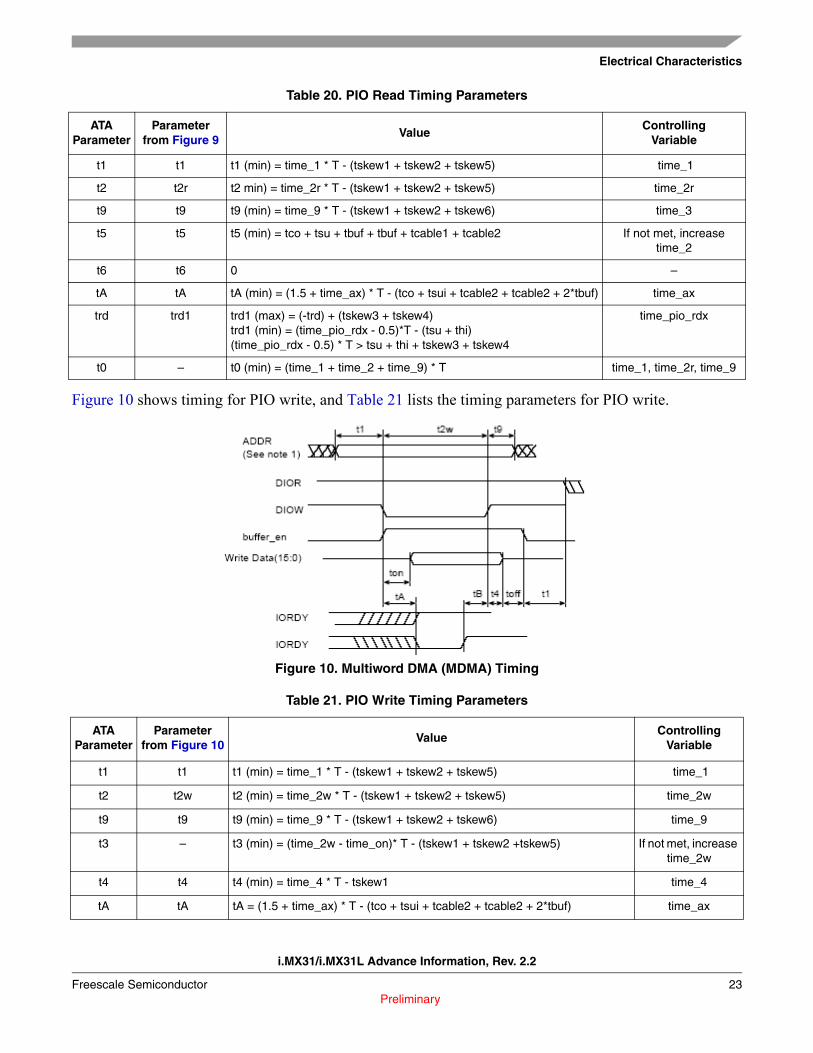
Figure 9 shows timing for PIO read, and Table 20 lists the timing parameters for PIO read.
Figure 9. PIO Read Timing Diagram
tco propagation delay bus clock L-to-H to ata_cs0, ata_cs1, ata_da2, ata_da1, ata_da0, ata_dior, ata_diow, ata_dmack, ata_data, ata_buffer_en
12.0 ns
tsu set-up time ata_data to bus clock L-to-H 8.5 ns
tsui set-up time ata_iordy to bus clock H-to-L 8.5 ns
thi hold time ata_iordy to bus clock H to L 2.5 ns
tskew1 Max difference in propagation delay bus clock L-to-H to any of following signalsata_cs0, ata_cs1, ata_da2, ata_da1, ata_da0, ata_dior, ata_diow, ata_dmack, ata_data (write), ata_buffer_en
7 ns
tskew2 Max difference in buffer propagation delay for any of following signalsata_cs0, ata_cs1, ata_da2, ata_da1, ata_da0, ata_dior, ata_diow, ata_dmack, ata_data (write), ata_buffer_en
transceiver
tskew3 Max difference in buffer propagation delay for any of following signals ata_iordy, ata_data (read)
transceiver
tbuf Max buffer propagation delay transceiver
tcable1 cable propagation delay for ata_data cable
tcable2 cable propagation delay for control signals ata_dior, ata_diow, ata_iordy, ata_dmack cable
tskew4 Max difference in cable propagation delay between ata_iordy and ata_data (read) cable
tskew5 Max difference in cable propagation delay between (ata_dior, ata_diow, ata_dmack) and ata_cs0, ata_cs1, ata_da2, ata_da1, ata_da0, ata_data(write)
cable
tskew6 Max difference in cable propagation delay without accounting for ground bounce cable
1 Values provided where applicable.
Table 19. ATA Timing Parameters (continued)
Name DescriptionValue/
Contributing Factor1
Electrical Characteristics
i.MX31/i.MX31L Advance Information, Rev. 2.2
Freescale Semiconductor 23 Preliminary
Figure 10 shows timing for PIO write, and Table 21 lists the timing parameters for PIO write.
Figure 10. Multiword DMA (MDMA) Timing
Table 20. PIO Read Timing Parameters
ATA Parameter
Parameter from Figure 9
ValueControlling
Variable
t1 t1 t1 (min) = time_1 * T - (tskew1 + tskew2 + tskew5) time_1
t2 t2r t2 min) = time_2r * T - (tskew1 + tskew2 + tskew5) time_2r
t9 t9 t9 (min) = time_9 * T - (tskew1 + tskew2 + tskew6) time_3
t5 t5 t5 (min) = tco + tsu + tbuf + tbuf + tcable1 + tcable2 If not met, increase time_2
t6 t6 0 –
tA tA tA (min) = (1.5 + time_ax) * T - (tco + tsui + tcable2 + tcable2 + 2*tbuf) time_ax
trd trd1 trd1 (max) = (-trd) + (tskew3 + tskew4)trd1 (min) = (time_pio_rdx - 0.5)*T - (tsu + thi)(time_pio_rdx - 0.5) * T > tsu + thi + tskew3 + tskew4
time_pio_rdx
t0 – t0 (min) = (time_1 + time_2 + time_9) * T time_1, time_2r, time_9
Table 21. PIO Write Timing Parameters
ATA Parameter
Parameter from Figure 10
ValueControlling
Variable
t1 t1 t1 (min) = time_1 * T - (tskew1 + tskew2 + tskew5) time_1
t2 t2w t2 (min) = time_2w * T - (tskew1 + tskew2 + tskew5) time_2w
t9 t9 t9 (min) = time_9 * T - (tskew1 + tskew2 + tskew6) time_9
t3 – t3 (min) = (time_2w - time_on)* T - (tskew1 + tskew2 +tskew5) If not met, increase time_2w
t4 t4 t4 (min) = time_4 * T - tskew1 time_4
tA tA tA = (1.5 + time_ax) * T - (tco + tsui + tcable2 + tcable2 + 2*tbuf) time_ax

i.MX31/i.MX31L Advance Information, Rev. 2.2
24 Freescale Semiconductor Preliminary
Electrical Characteristics
Figure 11 shows timing for MDMA read, Figure 12 shows timing for MDMA write, and Table 22 lists the timing parameters for MDMA read and write.
Figure 11. MDMA Read Timing Diagram
Figure 12. MDMA Write Timing Diagram
t0 – t0(min) = (time_1 + time_2 + time_9) * T time_1, time_2r, time_9
– – Avoid bus contention when switching buffer on by making ton long enough. –
– – Avoid bus contention when switching buffer off by making toff long enough. –
Table 22. MDMA Read and Write Timing Parameters
ATA Parameter
Parameter from
Figure 11, Figure 12
ValueControlling
Variable
tm, ti tm tm (min) = ti (min) = time_m * T - (tskew1 + tskew2 + tskew5) time_m
td td, td1 td1.(min) = td (min) = time_d * T - (tskew1 + tskew2 + tskew6) time_d
tk tk tk.(min) = time_k * T - (tskew1 + tskew2 + tskew6) time_k
Table 21. PIO Write Timing Parameters (continued)
ATA Parameter
Parameter from Figure 10
ValueControlling
Variable

Electrical Characteristics
i.MX31/i.MX31L Advance Information, Rev. 2.2
Freescale Semiconductor 25 Preliminary
4.3.5.3 UDMA In Timing
Figure 13 shows timing when the UDMA in transfer starts, Figure 14 shows timing when the UDMA in host terminates transfer, Figure 15 shows timing when the UDMA in device terminates transfer, and Table 23 lists the timing parameters for UDMA in burst.
Figure 13. UDMA In Transfer Starts Timing Diagram
t0 – t0 (min) = (time_d + time_k) * T time_d, time_k
tg(read) tgr tgr (min-read) = tco + tsu + tbuf + tbuf + tcable1 + tcable2tgr.(min-drive) = td - te(drive)
time_d
tf(read) tfr tfr (min-drive) = 0 –
tg(write) – tg (min-write) = time_d * T - (tskew1 + tskew2 + tskew5) time_d
tf(write) – tf (min-write) = time_k * T - (tskew1 + tskew2 + tskew6) time_k
tL – tL (max) = (time_d + time_k-2)*T - (tsu + tco + 2*tbuf + 2*tcable2) time_d, time_k
tn, tj tkjn tn= tj= tkjn = (max(time_k,. time_jn) * T - (tskew1 + tskew2 + tskew6) time_jn
– tontoff
ton = time_on * T - tskew1toff = time_off * T - tskew1
–
Table 22. MDMA Read and Write Timing Parameters (continued)
ATA Parameter
Parameter from
Figure 11, Figure 12
ValueControlling
Variable

i.MX31/i.MX31L Advance Information, Rev. 2.2
26 Freescale Semiconductor Preliminary
Electrical Characteristics
Figure 14. UDMA In Host Terminates Transfer Timing Diagram
Figure 15. UDMA In Device Terminates Transfer Timing Diagram
Table 23. UDMA In Burst Timing Parameters
ATA Parameter
Parameter from
Figure 13, Figure 14, Figure 15
Description Controlling Variable
tack tack tack (min) = (time_ack * T) - (tskew1 + tskew2) time_ack
tenv tenv tenv (min) = (time_env * T) - (tskew1 + tskew2)tenv (max) = (time_env * T) + (tskew1 + tskew2)
time_env
tds tds1 tds - (tskew3) - ti_ds > 0 tskew3, ti_ds, ti_dh should be low enough
tdh tdh1 tdh - (tskew3) -ti_dh > 0

Electrical Characteristics
i.MX31/i.MX31L Advance Information, Rev. 2.2
Freescale Semiconductor 27 Preliminary
4.3.5.4 UDMA Out Timing
Figure 16 shows timing when the UDMA out transfer starts, Figure 17 shows timing when the UDMA out host terminates transfer, Figure 18 shows timing when the UDMA out device terminates transfer, and Table 24 lists the timing parameters for UDMA out burst.
Figure 16. UDMA Out Transfer Starts Timing Diagram
tcyc tc1 (tcyc - tskew) > T T big enough
trp trp trp (min) = time_rp * T - (tskew1 + tskew2 + tskew6) time_rp
– tx11 (time_rp * T) - (tco + tsu + 3T + 2 *tbuf + 2*tcable2) > trfs (drive) time_rp
tmli tmli1 tmli1 (min) = (time_mlix + 0.4) * T time_mlix
tzah tzah tzah (min) = (time_zah + 0.4) * T time_zah
tdzfs tdzfs tdzfs = (time_dzfs * T) - (tskew1 + tskew2) time_dzfs
tcvh tcvh tcvh = (time_cvh *T) - (tskew1 + tskew2) time_cvh
– tontoff
ton = time_on * T - tskew1toff = time_off * T - tskew1
–
1 There is a special timing requirement in the ATA host that requires the internal DIOW to go only high 3 clocks after the last active edge on the DSTROBE signal. The equation given on this line tries to capture this constraint.
2. Make ton and toff big enough to avoid bus contention
Table 23. UDMA In Burst Timing Parameters (continued)
ATA Parameter
Parameter from
Figure 13, Figure 14, Figure 15
Description Controlling Variable

i.MX31/i.MX31L Advance Information, Rev. 2.2
28 Freescale Semiconductor Preliminary
Electrical Characteristics
Figure 17. UDMA Out Host Terminates Transfer Timing Diagram
Figure 18. UDMA Out Device Terminates Transfer Timing Diagram
Table 24. UDMA Out Burst Timing Parameters
ATA Parameter
Parameter from
Figure 16, Figure 17, Figure 18
ValueControlling
Variable
tack tack tack (min) = (time_ack * T) - (tskew1 + tskew2) time_ack
tenv tenv tenv (min) = (time_env * T) - (tskew1 + tskew2)tenv (max) = (time_env * T) + (tskew1 + tskew2)
time_env
tdvs tdvs tdvs = (time_dvs * T) - (tskew1 + tskew2) time_dvs
tdvh tdvh tdvs = (time_dvh * T) - (tskew1 + tskew2) time_dvh
tcyc tcyc tcyc = time_cyc * T - (tskew1 + tskew2) time_cyc
t2cyc – t2cyc = time_cyc * 2 * T time_cyc

Electrical Characteristics
i.MX31/i.MX31L Advance Information, Rev. 2.2
Freescale Semiconductor 29 Preliminary
4.3.6 AUDMUX Electrical Specifications
The AUDMUX provides a programmable interconnect logic for voice, audio and data routing between internal serial interfaces (SSI) and external serial interfaces (audio and voice codecs). The AC timing of AUDMUX external pins is hence governed by the SSI module. Please refer to their respective electrical specifications.
4.3.7 CSPI Electrical Specifications
This section describes the electrical information of the CSPI.
4.3.7.1 CSPI Timing
Figure 19 and Figure 20 depict the master mode and slave mode timings of CSPI, and Table 25 lists the timing parameters.
trfs1 trfs trfs = 1.6 * T + tsui + tco + tbuf + tbuf –
– tdzfs tdzfs = time_dzfs * T - (tskew1) time_dzfs
tss tss tss = time_ss * T - (tskew1 + tskew2) time_ss
tmli tdzfs_mli tdzfs_mli =max (time_dzfs, time_mli) * T - (tskew1 + tskew2) –
tli tli1 tli1 > 0 –
tli tli2 tli2 > 0 –
tli tli3 tli3 > 0 –
tcvh tcvh tcvh = (time_cvh *T) - (tskew1 + tskew2) time_cvh
– tontoff
ton = time_on * T - tskew1toff = time_off * T - tskew1
–
Table 24. UDMA Out Burst Timing Parameters (continued)
ATA Parameter
Parameter from
Figure 16, Figure 17, Figure 18
ValueControlling
Variable

i.MX31/i.MX31L Advance Information, Rev. 2.2
30 Freescale Semiconductor Preliminary
Electrical Characteristics
Figure 19. CSPI Master Mode Timing Diagram
NOTECSPI1_DRYN is connected to CSPI1_CS_1, and CSPI2_DRYN is connected to DAM2_T_CLK.
Figure 20. CSPI Slave Mode Timing Diagram
Table 25. CSPI Interface Timing Parameters
ID Parameter Symbol Min Max Units
CS1 CSPIx_CLK Cycle Time tclk 60 – ns
CS2 CSPIx_CLK High or Low Time tSW 30 – ns
CS3 CSPIx_CLK Rise or Fall tRISE/FALL – 7.6 ns
CS4 CSPIx_CS_x pulse width tCSLH 25 – ns
CS5 CSPIx_CS_x Lead Time (CS setup time) tSCS 25 – ns
CS6 CSPIx_CS_x Lag Time (CS hold time) tHCS 25 – ns
CS7 CSPIx_DO Setup Time tSmosi 5 – ns
CS8 CSPIx_DO Hold Time tHmosi 5 – ns
CS9 CSPIx_DI Setup Time tSmiso 5 – ns
CS1
CS7 CS8
CS2
CS2
CS4
CS6 CS5
CS9 CS10
CSPIx_CLK
CSPIx_CS_x
CSPIx_DO
CSPIx_DI
CSPIx_DRYNCS11
CS3
CS3
CS7 CS8
CS2
CS2
CS4CS6
CS9 CS10
CSPIx_CLK
CSPIx_CS_x
CSPIx_DI
CSPIx_DO
CS1 CS3
CS3
CS5

Electrical Characteristics
i.MX31/i.MX31L Advance Information, Rev. 2.2
Freescale Semiconductor 31 Preliminary
4.3.8 DPLL Electrical Specifications
The three PLL’s of the MX31/MX31L (MCU, USB, and Serial PLL) are all based on same DPLL design. The characteristics provided herein apply to all of them, except where noted explicitly. The PLL characteristics are provided based on measurements done for both sources—external clock source (CKIH), and FPM (Frequency Pre-Multiplier) source.
4.3.8.1 Electrical Specifications
Table 26 lists the DPLL specification.
CS10 CSPIx_DI Hold Time tHmiso 5 – ns
CS11 CSPIx_DRYN Setup Time tSDRY 5 – ns
Table 26. DPLL Specifications
Parameter Min Typ Max Unit Comments
CKIH frequency 15 261
1 The user or board designer must take into account that the use of a frequency other than 26 MHz would require adjustment to the DPTC-DVFS table, which is incorporated into operating system code.
752
2 The PLL reference frequency must be ≤ 35 MHz. Therefore, for frequencies between 35 MHz and 70 MHz, program the predivider to divide by 2 or more. If the CKIH frequency is above 70 MHz, program the predivider to 3 or more. For PD bit description, see the reference manual.
MHz –
CKIL frequency(Frequency Pre-multiplier (FPM) enable mode)
– 32; 32.768, 38.4 – kHz FPM lock time ≈ 480 µs.
Predivision factor (PD bits) 1 – 16 – –
PLL reference frequency range after Predivider 15 – 35 MHz 15 ≤ CKIH frequency/PD ≤ 35 MHz15 ≤ FPM output/PD ≤ 35 MHz
PLL output frequency range:MPLL and SPLL
UPLL52
190
–532240
MHz –
Maximum allowed reference clock phase noise. – – ± 100 ps –
Frequency lock time(FOL mode or non-integer MF)
– – 398 – Cycles of divided reference clock.
Phase lock time – – 100 µs In addition to the frequency
Maximum allowed PLL supply voltage ripple – – 25 mV Fmodulation < 50 kHz
Maximum allowed PLL supply voltage ripple – – 20 mV 50 kHz < Fmodulation < 300 kHz
Maximum allowed PLL supply voltage ripple – – 25 mV Fmodulation > 300 kHz
PLL output clock phase jitter – – 5.2 ns Measured on CLKO pin
PLL output clock period jitter – – 420 ps Measured on CLKO pin
Table 25. CSPI Interface Timing Parameters (continued)
ID Parameter Symbol Min Max Units

i.MX31/i.MX31L Advance Information, Rev. 2.2
32 Freescale Semiconductor Preliminary
Electrical Characteristics
4.3.9 EMI Electrical Specifications
This section provides electrical parametrics and timings for EMI module.
4.3.9.1 NAND Flash Controller Interface (NFC)
The MX31 NFC supports normal timing mode, using two flash clock cycles for one access of RE and WE. AC timings are provided as multiplications of the clock cycle and fixed delay. Figure 21, Figure 22, Figure 23, and Figure 24 depict the relative timing requirements among different signals of the NFC at module level, for normal mode, and Table 27 lists the timing parameters.
Figure 21. Command Latch Cycle Timing DIagram
Figure 22. Address Latch Cycle Timing DIagram
NFCLE
NFCE
NFWE
NFALE
NFIO[7:0] Command
NF9NF8
NF1 NF2
NF5
NF3 NF4
NF6 NF7
NFCLE
NFCE
NFWE
NFALE
NFIO[7:0] Address
NF9NF8
NF1
NF5
NF3 NF4
NF6
NF11
NF10
NF7

Electrical Characteristics
i.MX31/i.MX31L Advance Information, Rev. 2.2
Freescale Semiconductor 33 Preliminary
Figure 23. Write Data Latch Cycle Timing DIagram
Figure 24. Read Data Latch Cycle Timing DIagram
Table 27. NFC Timing Parameters1
ID Parameter Symbol
TimingT = NFC Clock Cycle2
Example Timing for NFC Clock ≈ 33 MHz
T = 30 ns Unit
Min Max Min Max
NF1 NFCLE Setup Time tCLS T–1.0 ns – 29 – ns
NF2 NFCLE Hold Time tCLH T–2.0 ns – 28 – ns
NF3 NFCE Setup Time tCS T–1.0 ns – 29 – ns
NF4 NFCE Hold Time tCH T–2.0 ns – 28 – ns
NFCLE
NFCE
NFWE
NFALE
NFIO[15:0] Data to NF
NF9NF8
NF1
NF5
NF3
NF6
NF11
NF10
NF7
NFCLE
NFCE
NFRE
NFRB
NFIO[15:0] Data from NF
NF13NF15
NF14
NF17
NF12
NF16

i.MX31/i.MX31L Advance Information, Rev. 2.2
34 Freescale Semiconductor Preliminary
Electrical Characteristics
NOTEHigh is defined as 80% of signal value and low is defined as 20% of signal value.
NOTETiming for HCLK is 133 MHz and internal NFC clock (flash clock) is approximately 33 MHz (30 ns). All timings are listed according to this NFC clock frequency (multiples of NFC clock phases), except NF16 and NF17, which are not NFC clock related.
4.3.9.2 Wireless External Interface Module (WEIM)
All WEIM output control signals may be asserted and deasserted by internal clock related to BCLK rising edge or falling edge according to corresponding assertion/negation control fields. Address always begins related to BCLK falling edge but may be ended both on rising and falling edge in muxed mode according to control register configuration. Output data begins related to BCLK rising edge except in muxed mode where both rising and falling edge may be used according to control register configuration. Input data, ECB and DTACK all captured according to BCLK rising edge time. Figure 25 depicts the timing of the WEIM module, and Table 28 lists the timing parameters.
NF5 NF_WP Pulse Width tWP T–1.5 ns 28.5 ns
NF6 NFALE Setup Time tALS T – 30 – ns
NF7 NFALE Hold Time tALH T–3.0 ns – 27 – ns
NF8 Data Setup Time tDS T – 30 – ns
NF9 Data Hold Time tDH T–5.0 ns – 25 – ns
NF10 Write Cycle Time tWC 2T 60 ns
NF11 NFWE Hold Time tWH T–2.5 ns 27.5 ns
NF12 Ready to NFRE Low tRR 6T – 180 – ns
NF13 NFRE Pulse Width tRP 1.5T – 45 – ns
NF14 READ Cycle Time tRC 2T – 60 – ns
NF15 NFRE High Hold Time tREH 0.5T–2.5 ns 12.5 – ns
NF16 Data Setup on READ tDSR N/A 10 – ns
NF17 Data Hold on READ tDHR N/A 0 – ns
1 The flash clock maximum frequency is 50 MHz.2 Subject to DPLL jitter specification on Table 26, "DPLL Specifications," on page 31.
Table 27. NFC Timing Parameters1 (continued)
ID Parameter Symbol
TimingT = NFC Clock Cycle2
Example Timing for NFC Clock ≈ 33 MHz
T = 30 ns Unit
Min Max Min Max

Electrical Characteristics
i.MX31/i.MX31L Advance Information, Rev. 2.2
Freescale Semiconductor 35 Preliminary
,
Figure 25. WEIM Bus Timing Diagram
Table 28. WEIM Bus Timing Parameters
ID Parameter Min Max Unit
WE1 Clock fall to Address Valid -0.5 2.5 ns
WE2 Clock rise/fall to Address Invalid -0.5 5 ns
WE3 Clock rise/fall to CS[x] Valid -3 3 ns
WE4 Clock rise/fall to CS[x] Invalid -3 3 ns
WE5 Clock rise/fall to RW Valid -3 3 ns
WE6 Clock rise/fall to RW Invalid -3 3 ns
WE7 Clock rise/fall to OE Valid -3 3 ns
WE1 WE2
WE3 WE4
WE5 WE6
WE7 WE8
WE9 WE10
WE11 WE12
WE13 WE14
WE16
WE15
WE18
WE17
WE20
WE19
WE21WE22
WE23BCLK
Address
CS[x]
RW
OE
EB[x]
LBA
Output Data
BCLK
Input Data
WEIM Outputs Timing
WEIM Inputs Timing
ECB
DTACK
...

i.MX31/i.MX31L Advance Information, Rev. 2.2
36 Freescale Semiconductor Preliminary
Electrical Characteristics
NOTEHigh is defined as 80% of signal value and low is defined as 20% of signal value.
Test conditions: load capacitance, 25 pF. Recommended drive strength for all controls, address, and BCLK is Max drive.
Figure 26, Figure 27, Figure 28, Figure 29, Figure 30, and Figure 31 depict some examples of basic WEIM accesses to external memory devices with the timing parameters mentioned in Table 28 for specific control parameter settings.
WE8 Clock rise/fall to OE Invalid -3 3 ns
WE9 Clock rise/fall to EB[x] Valid -3 3 ns
WE10 Clock rise/fall to EB[x] Invalid -3 3 ns
WE11 Clock rise/fall to LBA Valid -3 3 ns
WE12 Clock rise/fall to LBA Invalid -3 3 ns
WE13 Clock rise/fall to Output Data Valid - 2.5 + 4 ns
WE14 Clock rise to Output Data Invalid - 2.5 + 4 ns
WE15 Input Data Valid to Clock rise, FCE=0FCE=1
82.5
–ns
WE16 Clock rise to Input Data Invalid, FCE=0FCE=1
-2-2
–ns
WE17 ECB setup time, FCE=0FCE=1
6.53.5
–ns
WE18 ECB hold time, FCE=0FCE=1
-22
–ns
WE19 DTACK setup time1 0 – ns
WE20 DTACK hold time1 4.5 – ns
WE21 BCLK High Level Width2, 3 – Tcycle/2-3
ns
WE22 BCLK Low Level Width2, 3 – Tcycle/2-3
ns
WE23 BCLK Cycle time2 15 – ns
1 Applies to rising edge timing2 BCLK parameters are being measured from the 50% VDD.3 The actual cycle time is derived from the AHB bus clock frequency.
Table 28. WEIM Bus Timing Parameters (continued)
ID Parameter Min Max Unit

Electrical Characteristics
i.MX31/i.MX31L Advance Information, Rev. 2.2
Freescale Semiconductor 37 Preliminary
Figure 26. Asynchronous Memory Timing Diagram for Read Access—WSC=1
Figure 27. Asynchronous Memory Timing Diagram for Write Access—WSC=1, EBWA=1, EBWN=1, LBN=1
Last Valid Address V1
V1
BCLK
ADDR
DATA
RW
LBA
OE
EB[y]
CS[x]
Next Address
WE1 WE2
WE3 WE4
WE7 WE8
WE10WE9
WE11 WE12
WE15
WE16
Last Valid Address V1
V1
BCLK
ADDR
DATA
RW
LBA
OE
EB[y]
CS[x]
Next Address
WE1 WE2
WE3 WE4
WE5 WE6
WE9 WE10
WE11 WE12
WE13
WE14

i.MX31/i.MX31L Advance Information, Rev. 2.2
38 Freescale Semiconductor Preliminary
Electrical Characteristics
Figure 28. Synchronous Memory Timing Diagram for Two Non-Sequential Read Accesses—WSC=2, SYNC=1, DOL=0
Figure 29. Synchronous Memory TIming Diagram for Burst Write Access—BCS=1, WSC=4, SYNC=1, DOL=0, PSR=1
Last Valid Addr Address V1 Address V2
V1 V1+2 V2 V2+2
BCLK
ADDR
ECB
DATA Halfword Halfword
CS[x]
RW
LBA
OE
EB[y]
Halfword Halfword
WE1 WE2
WE4
WE7 WE8
WE9 WE10
WE11 WE12
WE15 WE15
WE16 WE16
WE17 WE17
WE18 WE18
WE3
Last Valid Addr
BCLK
ADDR
DATA
CS[x]
RW
LBA
OE
EB[y]
ECB
Address V1
V1 V1+4 V1+12V1+8
WE9
WE1 WE2
WE3 WE4
WE5 WE6
WE10
WE11
WE13 WE13
WE14 WE14WE17
WE18
WE12

Electrical Characteristics
i.MX31/i.MX31L Advance Information, Rev. 2.2
Freescale Semiconductor 39 Preliminary
Figure 30. Muxed A/D Mode Timing Diagram for Asynchronous Write Access—WSC=7, LBA=1, LBN=1, LAH=1
Figure 31. Muxed A/D Mode Timing Diagram for Asynchronous Read Access—WSC=7, LBA=1, LBN=1, LAH=1, OEA=7
4.3.9.3 ESDCTL Electrical Specifications
Figure 32, Figure 33, Figure 34, Figure 35, Figure 36, and Figure 37 depict the timings pertaining to the ESDCTL module, which interfaces Mobile DDR or SDR SDRAM. Table 29, Table 30, Table 31, Table 32, Table 33, and Table 34 list the timing parameters.
Write
BCLK
ADDR/
RW
LBA
OE
EB[y]
CS[x]
Address V1 Write DataLast Valid AddrM_DATA
WE1 WE2
WE3 WE4
WE6WE5
WE9 WE10
WE11 WE12
WE13
WE14
BCLK
ADDR/
RW
LBA
OE
EB[y]
CS[x]
Address V1 Read DataLast Valid AddrM_DATA
WE2
WE3
WE4
WE11WE12
WE7 WE8
WE9 WE10
WE15
WE16WE1

i.MX31/i.MX31L Advance Information, Rev. 2.2
40 Freescale Semiconductor Preliminary
Electrical Characteristics
Figure 32. SDRAM Read Cycle Timing Diagram
Table 29. DDR/SDR SDRAM Read Cycle Timing Parameters
ID Parameter Symbol Min Max Unit
SD1 SDRAM clock high-level width tCH 3.4 4.1 ns
SD2 SDRAM clock low-level width tCL 3.4 4.1 ns
SD3 SDRAM clock cycle time tCK 7.5 – ns
SD4 CS, RAS, CAS, WE, DQM, CKE setup time tCMS 2.0 – ns
SD5 CS, RAS, CAS, WE, DQM, CKE hold time tCMH 1.8 – ns
SD6 Address setup time tAS 2.0 – ns
SD7 Address hold time tAH 1.8 – ns
SD8 SDRAM access time tAC – 6.47 ns
SDCLK
WE
ADDR
DQ
DQM
COL/BA
Data
CS
CAS
RAS
Note: CKE is high during the read/write cycle.
SD4
SD1
SD3SD2
SD4
SD4
SD4
SD4
SD5
SD5
SD5
SD5
SD5
SD6SD7
SD10
SD8
SD9
SDCLK
ROW/BA

Electrical Characteristics
i.MX31/i.MX31L Advance Information, Rev. 2.2
Freescale Semiconductor 41 Preliminary
NOTESDR SDRAM CLK parameters are being measured from the 50% point—that is, high is defined as 50% of signal value and low is defined as 50% of signal value. SD1 + SD2 does not exceed 7.5 ns for 133 MHz.
NOTEThe timing parameters are similar to the ones used in SDRAM data sheets—that is, Table 29 indicates SDRAM requirements. All output signals are driven by the ESDCTL at the negative edge of SDCLK and the parameters are measured at maximum memory frequency.
SD9 Data out hold time1 tOH 1.2 – ns
SD10 Active to read/write command period tRC 10 – clock
1 Timing parameters are relevant only to SDR SDRAM. For the specific DDR SDRAM data related timing parameters, see Table 33 and Table 34.
Table 29. DDR/SDR SDRAM Read Cycle Timing Parameters (continued)
ID Parameter Symbol Min Max Unit

i.MX31/i.MX31L Advance Information, Rev. 2.2
42 Freescale Semiconductor Preliminary
Electrical Characteristics
Figure 33. SDR SDRAM Write Cycle Timing Diagram
Table 30. SDR SDRAM Write Timing Parameters
ID Parameter Symbol Min Max Unit
SD1 SDRAM clock high-level width tCH 3.4 4.1 ns
SD2 SDRAM clock low-level width tCL 3.4 4.1 ns
SD3 SDRAM clock cycle time tCK 7.5 – ns
SD4 CS, RAS, CAS, WE, DQM, CKE setup time tCMS 2.0 – ns
SD5 CS, RAS, CAS, WE, DQM, CKE hold time tCMH 1.8 – ns
SD6 Address setup time tAS 2.0 – ns
SD7 Address hold time tAH 1.8 – ns
SD11 Precharge cycle period1 tRP 1 4 clock
SD12 Active to read/write command delay1 tRCD 1 8 clock
CS
CAS
WE
RAS
ADDR
DQ
DQM
BA ROW / BA COL/BA
DATA
SD4
SD4
SD4SD4
SD5
SD5
SD5SD5
SD7SD6
SD12
SD13 SD14
SD11
SDCLK
SD1
SD3SD2
SDCLK

Electrical Characteristics
i.MX31/i.MX31L Advance Information, Rev. 2.2
Freescale Semiconductor 43 Preliminary
NOTESDR SDRAM CLK parameters are being measured from the 50% point—that is, high is defined as 50% of signal value and low is defined as 50% of signal value.
NOTEThe timing parameters are similar to the ones used in SDRAM data sheets—that is, Table 30 indicates SDRAM requirements. All output signals are driven by the ESDCTL at the negative edge of SDCLK and the parameters are measured at maximum memory frequency.
Figure 34. SDRAM Refresh Timing Diagram
SD13 Data setup time tDS 2.0 – ns
SD14 Data hold time tDH 1.3 – ns
1 SD11 and SD12 are determined by SDRAM controller register settings.
Table 30. SDR SDRAM Write Timing Parameters (continued)
ID Parameter Symbol Min Max Unit
CS
CAS
WE
RAS
ADDR BA ROW/BA
SD6SD7
SD11
SD10 SD10
SDCLK
SD1
SD2
SDCLK
SD3

i.MX31/i.MX31L Advance Information, Rev. 2.2
44 Freescale Semiconductor Preliminary
Electrical Characteristics
NOTESDR SDRAM CLK parameters are being measured from the 50% point—that is, high is defined as 50% of signal value and low is defined as 50% of signal value.
NOTEThe timing parameters are similar to the ones used in SDRAM data sheets—that is, Table 31 indicates SDRAM requirements. All output signals are driven by the ESDCTL at the negative edge of SDCLK and the parameters are measured at maximum memory frequency.
Table 31. SDRAM Refresh Timing Parameters
ID Parameter Symbol Min Max Unit
SD1 SDRAM clock high-level width tCH 3.4 4.1 ns
SD2 SDRAM clock low-level width tCL 3.4 4.1 ns
SD3 SDRAM clock cycle time tCK 7.5 – ns
SD6 Address setup time tAS 1.8 – ns
SD7 Address hold time tAH 1.8 – ns
SD10 Precharge cycle period1
1 SD10 and SD11 are determined by SDRAM controller register settings.
tRP 1 4 clock
SD11 Auto precharge command period1 tRC 2 20 clock

Electrical Characteristics
i.MX31/i.MX31L Advance Information, Rev. 2.2
Freescale Semiconductor 45 Preliminary
Figure 35. SDRAM Self-Refresh Cycle Timing Diagram
NOTEThe clock will continue to run unless both CKEs are low. Then the clock will be stopped in low state.
Table 32. SDRAM Self-Refresh Cycle Timing Parameters
ID Parameter Symbol Min Max Unit
SD16 CKE output delay time tCKS 1.8 – ns
SDCLK
CS
CAS
RAS
ADDR BA
WE
CKE
Don’t care
SD16 SD16

i.MX31/i.MX31L Advance Information, Rev. 2.2
46 Freescale Semiconductor Preliminary
Electrical Characteristics
Figure 36. Mobile DDR SDRAM Write Cycle Timing Diagram
NOTESDRAM CLK and DQS related parameters are being measured from the 50% point—that is, high is defined as 50% of signal value and low is defined as 50% of signal value.
NOTEThe timing parameters are similar to the ones used in SDRAM data sheets—that is, Table 33 indicates SDRAM requirements. All output signals are driven by the ESDCTL at the negative edge of SDCLK and the parameters are measured at maximum memory frequency.
Table 33. Mobile DDR SDRAM Write Cycle Timing Parameters1
1 Test condition: Measured using delay line 5 programmed as follows: ESDCDLY5[15:0] = 0x0703.
ID Parameter Symbol Min Max Unit
SD17 DQ & DQM setup time to DQS tDS 0.95 – ns
SD18 DQ & DQM hold time to DQS tDH 0.95 – ns
SD19 Write cycle DQS falling edge to SDCLK output delay time. tDSS 1.8 – ns
SD20 Write cycle DQS falling edge to SDCLK output hold time. tDSH 1.8 – ns
SDCLK
SDCLK
DQS (output)
DQ (output)
DQM (output)
Data Data Data Data Data Data Data Data
DM DM DM DM DM DM DM DM
SD17
SD17
SD17
SD17
SD18SD18
SD18 SD18
SD19 SD20

Electrical Characteristics
i.MX31/i.MX31L Advance Information, Rev. 2.2
Freescale Semiconductor 47 Preliminary
Figure 37. Mobile DDR SDRAM DQ versus DQS and SDCLK Read Cycle Timing Diagram
NOTESDRAM CLK and DQS related parameters are being measured from the 50% point—that is, high is defined as 50% of signal value and low is defined as 50% of signal value.
NOTEThe timing parameters are similar to the ones used in SDRAM data sheets—that is, Table 34 indicates SDRAM requirements. All output signals are driven by the ESDCTL at the negative edge of SDCLK and the parameters are measured at maximum memory frequency.
4.3.10 ETM Electrical Specifications
ETM is an ARM protocol. The timing specifications in this section are given as a guide for a TPA that supports TRACECLK frequencies up to 133 MHz.
Figure 38 depicts the TRACECLK timings of ETM, and Table 35 lists the timing parameters.
Figure 38. ETM TRACECLK Timing Diagram
Table 34. Mobile DDR SDRAM Read Cycle Timing Parameters
ID Parameter Symbol Min Max Unit
SD21 DQS - DQ Skew (defines the Data valid window in read cycles related to DQS). tDQSQ – 0.85 ns
SD22 DQS DQ HOLD time from DQS tQH 2.3 – ns
SD23 DQS output access time from SDCLK posedge tDQSCK – 6.7 ns
SDCLK
SDCLK
DQS (input)
DQ (input) DataDataDataDataDataDataDataData
SD23
SD21SD22

i.MX31/i.MX31L Advance Information, Rev. 2.2
48 Freescale Semiconductor Preliminary
Electrical Characteristics
Figure 39 depicts the setup and hold requirements of the trace data pins with respect to TRACECLK, and Table 36 lists the timing parameters.
Figure 39. Trace Data Timing Diagram
4.3.10.1 Half-Rate Clocking Mode
When half-rate clocking is used, the trace data signals are sampled by the TPA on both the rising and falling edges of TRACECLK, where TRACECLK is half the frequency of the clock shown in Figure 39.
4.3.11 FIR Electrical Specifications
FIR implements asynchronous infrared protocols (FIR, MIR) that are defined by IrDA® (Infrared Data Association). Refer to http://www.IrDA.org for details on FIR and MIR protocols.
4.3.12 Fusebox Electrical Specifications
Table 35. ETM TRACECLK Timing Parameters
ID Parameter Min Max Unit
Tcyc Clock period Frequency dependent – ns
Twl Low pulse width 2 – ns
Twh High pulse width 2 – ns
Tr Clock and data rise time – 3 ns
Tf Clock and data fall time – 3 ns
Table 36. ETM Trace Data Timing Parameters
ID Parameter Min Max Unit
Ts Data setup 2 – ns
Th Data hold 1 – ns
Table 37. Fusebox Timing Characteristics
Ref. Num Description Symbol Minimum Typical Maximum Units
1 Program time for eFuse1
1 The program length is defined by the value defined in the epm_pgm_length[2:0] bits of the IIM module. The value to program is based on a 32 kHz clock source (4 * 1/32 kHz = 125 µs)
tprogram 125 – – µs

Electrical Characteristics
i.MX31/i.MX31L Advance Information, Rev. 2.2
Freescale Semiconductor 49 Preliminary
4.3.13 I2C Electrical Specifications
This section describes the electrical information of the I2C Module.
4.3.13.1 I2C Module Timing
Figure 40 depicts the timing of I2C module. Table 38 lists the I2C module timing parameters where the I/O supply is 2.7 V. 1
Figure 40. I2C Bus Timing Diagram
Table 38. I2C Module Timing Parameters—I2C Pin I/O Supply=2.7 V
ID ParameterStandard Mode Fast Mode
UnitMin Max Min Max
IC1 I2CLK cycle time 10 – 2.5 – μs
IC2 Hold time (repeated) START condition 4.0 – 0.6 – μs
IC3 Set-up time for STOP condition 4.0 – 0.6 – μs
IC4 Data hold time 01
1 A device must internally provide a hold time of at least 300 ns for I2DAT signal in order to bridge the undefined region of the falling edge of I2CLK.
3.452
2 The maximum hold time has to be met only if the device does not stretch the LOW period (ID IC6) of the I2CLK signal.
01 0.92 μs
IC5 HIGH Period of I2CLK Clock 4.0 – 0.6 – μs
IC6 LOW Period of the I2CLK Clock 4.7 – 1.3 – μs
IC7 Set-up time for a repeated START condition 4.7 – 0.6 – μs
IC8 Data set-up time 250 – 1003
3 A Fast-mode I2C-bus device can be used in a standard-mode I2C-bus system, but the requirement of set-up time (ID IC7) of 250 ns must then be met. This will automatically be the case if the device does not stretch the LOW period of the I2CLK signal.
If such a device does stretch the LOW period of the I2CLK signal, it must output the next data bit to the I2DAT line max_rise_time (ID No IC10) + data_setup_time (ID No IC8) = 1000 + 250 = 1250 ns (according to the Standard-mode I2C-bus specification) before the I2CLK line is released.
– ns
IC9 Bus free time between a STOP and START condition 4.7 – 1.3 – μs
IC10 Rise time of both I2DAT and I2CLK signals – 1000 20+0.1Cb4
4 Cb = total capacitance of one bus line in pF.
300 ns
IC11 Fall time of both I2DAT and I2CLK signals – 300 20+0.1Cb4 300 ns
IC12 Capacitive load for each bus line (Cb) – 400 – 400 pF
IC10 IC11 IC9
IC2 IC8 IC4 IC7 IC3
IC6
IC10
IC5
IC11 START STOP STARTSTART
I2DAT
I2CLK
IC1

i.MX31/i.MX31L Advance Information, Rev. 2.2
50 Freescale Semiconductor Preliminary
Electrical Characteristics
4.3.14 IPU—Sensor Interfaces
4.3.14.1 Supported Camera Sensors
Table 39 lists the known supported camera sensors at the time of publication.
4.3.14.2 Functional Description
There are three timing modes supported by the IPU.
4.3.14.2.1 Pseudo BT.656 Video Mode
Smart camera sensors, which include imaging processing, usually support video mode transfer. They use an embedded timing syntax to replace the SENSB_VSYNC and SENSB_HSYNC signals. The timing syntax is defined by the BT.656 standard.
This operation mode follows the recommendations of ITU BT.656 specifications. The only control signal used is SENSB_PIX_CLK. Start-of-frame and active-line signals are embedded in the data stream. An active line starts with a SAV code and ends with a EAV code. In some cases, digital blanking is inserted in between EAV and SAV code. The CSI decodes and filters out the timing-coding from the data stream, thus recovering SENSB_VSYNC and SENSB_HSYNC signals for internal use.
Table 39. Supported Camera Sensors1
1 Freescale Semiconductor does not recommend one supplier over another and in no way suggests that these are the only camera suppliers.
Vendor Model
Conexant CX11646, CX204902, CX204502
2 These sensors not validated at time of publication.
Agilant HDCP-2010, ADCS-10212, ADCS-10212
Toshiba TC90A70
ICMedia ICM202A, ICM1022
iMagic IM8801
Transchip TC5600, TC5600J, TC5640, TC5700, TC6000
Fujitsu MB86S02A
Micron MI-SOC-0133
Matsushita MN39980
STMicro W6411, W6500, W65012, W66002, W65522, STV09742
OmniVision OV7620, OV6630
Sharp LZ0P3714 (CCD)
Motorola MC30300 (Python)2, SCM200142, SCM201142, SCM221142, SCM200272
National Semiconductor LM96182

Electrical Characteristics
i.MX31/i.MX31L Advance Information, Rev. 2.2
Freescale Semiconductor 51 Preliminary
4.3.14.2.2 Gated Clock Mode
The SENSB_VSYNC, SENSB_HSYNC, and SENSB_PIX_CLK signals are used in this mode. See Figure 41.
Figure 41. Gated Clock Mode Timing Diagram
A frame starts with a rising edge on SENSB_VSYNC (all the timings correspond to straight polarity of the corresponding signals). Then SENSB_HSYNC goes to high and hold for the entire line. Pixel clock is valid as long as SENSB_HSYNC is high. Data is latched at the rising edge of the valid pixel clocks. SENSB_HSYNC goes to low at the end of line. Pixel clocks then become invalid and the CSI stops receiving data from the stream. For next line the SENSB_HSYNC timing repeats. For next frame the SENSB_VSYNC timing repeats.
4.3.14.2.3 Non-Gated Clock Mode
The timing is the same as the gated-clock mode (described in Section 4.3.14.2.2, “Gated Clock Mode” on page 51), except for the SENSB_HSYNC signal, which is not used. See Figure 42. All incoming pixel clocks are valid and will cause data to be latched into the input FIFO. The SENSB_PIX_CLK signal is inactive (states low) until valid data is going to be transmitted over the bus.
Figure 42. Non-Gated Clock Mode Timing Diagram
SENSB_VSYNC
SENSB_HSYNC
SENSB_PIX_CLK
SENSB_DATA[9:0] invalid
1st byte
n+1th frame
invalid
1st byte
nth frame
Active LineStart of Frame
SENSB_VSYNC
SENSB_PIX_CLK
SENSB_DATA[7:0] invalid
1st byte
n+1th frame
invalid
1st byte
nth frame
Start of Frame

i.MX31/i.MX31L Advance Information, Rev. 2.2
52 Freescale Semiconductor Preliminary
Electrical Characteristics
The timing described in Figure 42 is that of a Motorola sensor. Some other sensors may have a slightly different timing. The CSI can be programmed to support rising/falling-edge triggered SENSB_VSYNC; active-high/low SENSB_HSYNC; and rising/falling-edge triggered SENSB_PIX_CLK.
4.3.14.3 Electrical Characteristics
Figure 43 depicts the sensor interface timing, and Table 40 lists the timing parameters.
Figure 43. Sensor Interface Timing Diagram
4.3.15 IPU—Display Interfaces
4.3.15.1 Supported Display Components
Table 41 lists the known supported display components at the time of publication.
Table 40. Sensor Interface Timing Parameters
ID Parameter Symbol Min. Max. Units
IP1 Sensor input clock frequency Fmck 0.01 133 MHz
IP2 Data and control setup time Tsu 5 – ns
IP3 Data and control holdup time Thd 3 – ns
IP4 Sensor output (pixel) clock frequency Fpck 0.01 133 MHz
SENSB_MCLK
IP3
SENSB_DATA,SENSB_VSYNC,
IP2
1/IP1
1/IP4
SENSB_PIX_CLK
(Sensor Input)
(Sensor Output)
SENSB_HSYNC

Electrical Characteristics
i.MX31/i.MX31L Advance Information, Rev. 2.2
Freescale Semiconductor 53 Preliminary
4.3.15.2 Synchronous Interfaces
4.3.15.2.1 Interface to Active Matrix TFT LCD Panels, Functional Description
Figure 44 depicts the LCD interface timing for a generic active matrix color TFT panel. In this figure signals are shown with negative polarity. The sequence of events for active matrix interface timing is:
• DISPB_D3_CLK latches data into the panel on its negative edge (when positive polarity is selected). In active mode, DISPB_D3_CLK runs continuously.
• DISPB_D3_HSYNC causes the panel to start a new line.• DISPB_D3_VSYNC causes the panel to start a new frame. It always encompasses at least one
HSYNC pulse.
Table 41. Supported Display Components1
1 Freescale Semiconductor does not recommend one supplier over another and in no way suggests that these are the only display component suppliers.
Type Vendor Model
TFT displays (memory-less)
Sharp (HR-TFT Super Mobile LCD family)
LQ035Q7 DB02, LM019LC1Sxx
Samsung (QCIF and QVGA TFT modules for mobile phones)
LTS180S1-HF1, LTS180S3-HF1, LTS350Q1-PE1,LTS350Q1-PD1, LTS220Q1-HE12
2 These display components not validated at time of publication.
Toshiba (LTM series) LTM022P8062, LTM04C380K2,LTM018A02A2, LTM020P3322, LTM021P3372, LTM019P3342, LTM022A7832, LTM022A05ZZ2
NEC NL6448BC20-08E, NL8060BC31-27
Display controllers Epson S1D15xxx series, S1D19xxx series, S1D13713, S1D13715
Solomon Systech SSD1301 (OLED), SSD1828 (LDCD)
Hitachi HD66766, HD66772
ATI W2300
Smart display modules Epson L1F10043 T2, L1F10044 T2, L1F10045 T2, L2D220022, L2D200142, L2F500322, L2D25001 T2
Hitachi 120 160 65K/4096 C-STN (#3284 LTD-1398-2) based on HD 66766 controller
Densitron Europe LTD All displays with MPU 80/68K series interface and serial peripheral interface
Sharp LM019LC1Sxx
Sony ACX506AKM
Digital video encoders (for TV)
Analog Devices ADV7174/7179
Crystal (Cirrus Logic) CS49xx series
Focus FS453/4

i.MX31/i.MX31L Advance Information, Rev. 2.2
54 Freescale Semiconductor Preliminary
Electrical Characteristics
• DISPB_D3_DRDY acts like an output enable signal to the CRT display. This output enables the data to be shifted onto the display. When disabled, the data is invalid and the trace is off.
Figure 44. Interface Timing Diagram for TFT (Active Matrix) Panels
4.3.15.2.2 Interface to Active Matrix TFT LCD Panels, Electrical Characteristics
Figure 45 depicts the horizontal timing (timing of one line), including both the horizontal sync pulse and the data. All figure parameters shown are programmable. The timing images correspond to inverse polarity of the DISPB_D3_CLK signal and active-low polarity of the DISPB_D3_HSYNC, DISPB_D3_VSYNC and DISPB_D3_DRDY signals.
Figure 45. TFT Panels Timing Diagram—Horizontal Sync Pulse
Figure 46 depicts the vertical timing (timing of one frame). All figure parameters shown are programmable.
DISPB_D3_CLK
1 2 3 mm-1
DISPB_D3_HSYNC
DISPB_D3_VSYNC
DISPB_D3_HSYNC
LINE 1 LINE 2 LINE 3 LINE 4 LINE n-1 LINE n
DISPB_D3_DRDY
DISPB_D3_DATA
DISPB_D3_HSYNC
DISPB_D3_DRDY
DISPB_D3_DATA
DISPB_D3_CLK
IP7
IP9 IP10
IP8
Start of line IP5
IP6

Electrical Characteristics
i.MX31/i.MX31L Advance Information, Rev. 2.2
Freescale Semiconductor 55 Preliminary
Figure 46. TFT Panels Timing Diagram—Vertical Sync Pulse
Table 42 shows timing parameters of signals presented in Figure 45 and Figure 46.Table 42. Synchronous Display Interface Timing Parameters—Pixel Level
ID Parameter Symbol Value Units
IP5 Display interface clock period Tdicp Tdicp1
1 Display interface clock period immediate value.
Display interface clock period average value.
ns
IP6 Display pixel clock period Tdpcp (DISP3_IF_CLK_CNT_D+1) * Tdicp ns
IP7 Screen width Tsw (SCREEN_WIDTH+1) * Tdpcp ns
IP8 HSYNC width Thsw (H_SYNC_WIDTH+1) * Tdpcp ns
IP9 Horizontal blank interval 1 Thbi1 BGXP * Tdpcp ns
IP10 Horizontal blank interval 2 Thbi2 (SCREEN_WIDTH - BGXP - FW) * Tdpcp ns
IP11 HSYNC delay Thsd H_SYNC_DELAY * Tdpcp ns
IP12 Screen height Tsh (SCREEN_HEIGHT+1) * Tsw ns
IP13 VSYNC width Tvsw if V_SYNC_WIDTH_L = 0 than(V_SYNC_WIDTH+1) * Tdpcpelse(V_SYNC_WIDTH+1) * Tsw
ns
IP14 Vertical blank interval 1 Tvbi1 BGYP * Tsw ns
IP15 Vertical blank interval 2 Tvbi2 (SCREEN_HEIGHT - BGYP - FH) * Tsw ns
IP14
DISPB_D3_VSYNC
DISPB_D3_HSYNC
DISPB_D3_DRDY
Start of frame End of frame
IP12
IP15
IP13
IP11
TdicpTHSP_CLK
DISP3_IF_CLK_PER_WRHSP_CLK_PERIOD
------------------------------------------------------------------⋅ for integer DISP3_IF_CLK_PER_WRHSP_CLK_PERIOD
------------------------------------------------------------------,
THSP_CLK floor DISP3_IF_CLK_PER_WRHSP_CLK_PERIOD
------------------------------------------------------------------ 0.5 0.5±+⎝ ⎠⎛ ⎞⋅ for fractional DISP3_IF_CLK_PER_WR
HSP_CLK_PERIOD------------------------------------------------------------------,
⎩⎪⎪⎨⎪⎪⎧
=
Tdicp THSP_CLKDISP3_IF_CLK_PER_WR
HSP_CLK_PERIOD------------------------------------------------------------------⋅=

i.MX31/i.MX31L Advance Information, Rev. 2.2
56 Freescale Semiconductor Preliminary
Electrical Characteristics
NOTEHSP_CLK is the High-Speed Port Clock, which is the input to the Image Processing Unit (IPU). Its frequency is controlled by the Clock Control Module (CCM) settings. The HSP_CLK frequency must be greater than or equal to the AHB clock frequency.
The SCREEN_WIDTH, SCREEN_HEIGHT, H_SYNC_WIDTH, V_SYNC_WIDTH, BGXP, BGYP and V_SYNC_WIDTH_L parameters are programmed via the SDC_HOR_CONF, SDC_VER_CONF, SDC_BG_POS Registers. The FW and FH parameters are programmed for the corresponding DMA channel. The DISP3_IF_CLK_PER_WR, HSP_CLK_PERIOD and DISP3_IF_CLK_CNT_D parameters are programmed via the DI_DISP3_TIME_CONF, DI_HSP_CLK_PER and DI_DISP_ACC_CC Registers.
Figure 47 depicts the synchronous display interface timing for access level, and Table 43 lists the timing parameters. The DISP3_IF_CLK_DOWN_WR and DISP3_IF_CLK_UP_WR parameters are set via the DI_DISP3_TIME_CONF Register.
Figure 47. Synchronous Display Interface Timing Diagram—Access Level
Table 43. Synchronous Display Interface Timing Parameters—Access Level
ID Parameter Symbol Min Typ1
1 The exact conditions have not been finalized, but will likely match the current customer requirement for their specific display. These conditions may be device specific.
Max Units
IP16 Display interface clock low time Tckl Tdicd-Tdicu-1.5 Tdicd2-Tdicu3
2 Display interface clock down time
Tdicd-Tdicu+1.5 ns
IP17 Display interface clock high time Tckh Tdicp-Tdicd+Tdicu-1.5 Tdicp-Tdicd+Tdicu Tdicp-Tdicd+Tdicu+1.5 ns
IP18 Data setup time Tdsu Tdicd-3.5 Tdicu – ns
IP19 Data holdup time Tdhd Tdicp-Tdicd-3.5 Tdicp-Tdicu – ns
IP20 Control signals setup time to display interface clock
Tcsu Tdicd-3.5 Tdicu – ns
IP19
DISPB_D3_CLK
DISPB_DATA
IP18
IP20DISPB_D3_VSYNC
IP17IP16
DISPB_D3_DRDYDISPB_D3_HSYNC
other controls
Tdicd 12---THSP_CLK ceil 2 DISP3_IF_CLK_DOWN_WR⋅
HSP_CLK_PERIOD---------------------------------------------------------------------------------⋅=

Electrical Characteristics
i.MX31/i.MX31L Advance Information, Rev. 2.2
Freescale Semiconductor 57 Preliminary
4.3.15.3 Interface to Sharp HR-TFT Panels
Figure 48 depicts the Sharp HR-TFT panel interface timing, and Table 44 lists the timing parameters. The CLS_RISE_DELAY, CLS_FALL_DELAY, PS_FALL_DELAY, PS_RISE_DELAY, REV_TOGGLE_DELAY parameters are defined in the SDC_SHARP_CONF_1 and SDC_SHARP_CONF_2 registers. For other Sharp interface timing characteristics, refer to Section 4.3.15.2.2, “Interface to Active Matrix TFT LCD Panels, Electrical Characteristics” on page 54. The timing images correspond to straight polarity of the Sharp signals.
Figure 48. Sharp HR-TFT Panel Interface Timing Diagram—Pixel Level
3 Display interface clock up time
where CEIL(X) rounds the elements of X to the nearest integers towards infinity.
Tdicu 12---THSP_CLK ceil 2 DISP3_IF_CLK_UP_WR⋅
HSP_CLK_PERIOD----------------------------------------------------------------------⋅=
D1 D2
DISPB_D3_CLK
DISPB_D3_DATA
DISPB_D3_SPL
DISPB_D3_HSYNC
DISPB_D3_CLS
DISPB_D3_PS
DISPB_D3_REV
1 DISPB_D3_CLK period
IP26
D320
Horizontal timing
IP22
IP23
IP25
IP21
IP24
Example is drawn with FW+1=320 pixel/line, FH+1=240 lines.SPL pulse width is fixed and aligned to the first data of the line.REV toggles every HSYNC period.

i.MX31/i.MX31L Advance Information, Rev. 2.2
58 Freescale Semiconductor Preliminary
Electrical Characteristics
4.3.15.4 Synchronous Interface to Dual-Port Smart Displays
Functionality and electrical characteristics of the synchronous interface to dual-port smart displays are identical to parameters of the synchronous interface. See Section 4.3.15.2.2, “Interface to Active Matrix TFT LCD Panels, Electrical Characteristics” on page 54.
4.3.15.4.1 Interface to a TV Encoder, Functional Description
The interface has an 8-bit data bus, transferring a single 8-bit value (Y/U/V) in each cycle. The bits D7–D0 of the value are mapped to bits LD17–LD10 of the data bus, respectively. Figure 49 depicts the interface timing,
• The frequency of the clock DISPB_D3_CLK is 27 MHz (within 10%).• The DISPB_D3_HSYNC, DISPB_D3_VSYNC and DISPB_D3_DRDY signals are active low.• The transition to the next row is marked by the negative edge of the DISPB_D3_HSYNC signal.
It remains low for a single clock cycle.• The transition to the next field/frame is marked by the negative edge of the DISPB_D3_VSYNC
signal. It remains low for at least one clock cycle.— At a transition to an odd field (of the next frame), the negative edges of DISPB_D3_VSYNC
and DISPB_D3_HSYNC coincide.— At a transition to an even field (of the same frame), they do not coincide.
• The active intervals—during which data is transferred—are marked by the DISPB_D3_HSYNC signal being high.
Table 44. Sharp Synchronous Display Interface Timing Parameters—Pixel Level
ID Parameter Symbol Value Units
IP21 SPL rise time Tsplr (BGXP - 1) * Tdpcp ns
IP22 CLS rise time Tclsr CLS_RISE_DELAY * Tdpcp ns
IP23 CLS fall time Tclsf CLS_FALL_DELAY * Tdpcp ns
IP24 CLS rise and PS fall time Tpsf PS_FALL_DELAY * Tdpcp ns
IP25 PS rise time Tpsr PS_RISE_DELAY * Tdpcp ns
IP26 REV toggle time Trev REV_TOGGLE_DELAY * Tdpcp ns

Electrical Characteristics
i.MX31/i.MX31L Advance Information, Rev. 2.2
Freescale Semiconductor 59 Preliminary
Figure 49. TV Encoder Interface Timing Diagram
DISPB_D3_CLK
DISPB_D3_HSYNC
DISPB_DATA
DISPB_D3_VSYNC
Cb Y CrCb Y Cr Y
Pixel Data Timing
Line and Field Timing - NTSC
Even Field Odd Field
Odd Field Even Field
624621
311308
Line and Field Timing - PAL
DISPB_D3_HSYNC
DISPB_D3_DRDY
DISPB_D3_VSYNC
DISPB_D3_HSYNC
DISPB_D3_DRDY
DISPB_D3_VSYNC
Even Field Odd Field
Odd Field Even Field
1523
262261
DISPB_D3_DRDY
DISPB_D3_HSYNC
DISPB_D3_DRDY
DISPB_D3_VSYNC
DISPB_D3_HSYNC
DISPB_D3_VSYNC
524 525 2 3 4 10
263 264 265 266 267 268 269 273
622 623 625 1 2 23
309 310 312 313 314 336
5 6
3 4
316315
DISPB_D3_DRDY

i.MX31/i.MX31L Advance Information, Rev. 2.2
60 Freescale Semiconductor Preliminary
Electrical Characteristics
4.3.15.4.2 Interface to a TV Encoder, Electrical Characteristics
The timing characteristics of the TV encoder interface are identical to the synchronous display characteristics. See Section 4.3.15.2.2, “Interface to Active Matrix TFT LCD Panels, Electrical Characteristics” on page 54.
4.3.15.5 Asynchronous Interfaces
4.3.15.5.1 Parallel Interfaces, Functional Description
The IPU supports the following asynchronous parallel interfaces:• System 80 interface
— Type 1 (sampling with the chip select signal) with and without byte enable signals.— Type 2 (sampling with the read and write signals) with and without byte enable signals.
• System 68k interface— Type 1 (sampling with the chip select signal) with or without byte enable signals.— Type 2 (sampling with the read and write signals) with or without byte enable signals.
For each of four system interfaces, there are three burst modes:1. Burst mode without a separate clock. The burst length is defined by the corresponding parameters
of the IDMAC (when data is transferred from the system memory) of by the HBURST signal (when the MCU directly accesses the display via the slave AHB bus). For system 80 and system 68k type 1 interfaces, data is sampled by the CS signal and other control signals changes only when transfer direction is changed during the burst. For type 2 interfaces, data is sampled by the WR/RD signals (system 80) or by the ENABLE signal (system 68k) and the CS signal stays active during the whole burst.
2. Burst mode with the separate clock DISPB_BCLK. In this mode, data is sampled with the DISPB_BCLK clock. The CS signal stays active during whole burst transfer. Other controls are changed simultaneously with data when the bus state (read, write or wait) is altered. The CS signals and other controls move to non-active state after burst has been completed.
3. Single access mode. In this mode, slave AHB and DMA burst are broken to single accesses. The data is sampled with CS or other controls according the interface type as described above. All controls (including CS) become non-active for one display interface clock after each access. This mode corresponds to the ATI single access mode.
Both system 80 and system 68k interfaces are supported for all described modes as depicted in Figure 50, Figure 51, Figure 52, and Figure 53. These timing images correspond to active-low DISPB_D#_CS, DISPB_D#_WR and DISPB_D#_RD signals.
Additionally, the IPU allows a programmable pause between two burst. The pause is defined in the HSP_CLK cycles. It allows to avoid timing violation between two sequential bursts or two accesses to different displays. The range of this pause is from 4 to 19 HSP_CLK cycles.

Electrical Characteristics
i.MX31/i.MX31L Advance Information, Rev. 2.2
Freescale Semiconductor 61 Preliminary
Figure 50. Asynchronous Parallel System 80 Interface (Type 1) Burst Mode Timing Diagram
DISPB_D#_CS
DISPB_PAR_RS
DISPB_WR
DISPB_RD
DISPB_DATA
DISPB_BCLK
DISPB_D#_CS
DISPB_PAR_RS
DISPB_WR
DISPB_RD
DISPB_DATA
DISPB_D#_CS
DISPB_PAR_RS
DISPB_WR
DISPB_RD
DISPB_DATA
Burst access mode with sampling by CS signal
Burst access mode with sampling by separate burst clock (BCLK)
Single access mode (all control signals are not active for one display interface clock after each display access)

i.MX31/i.MX31L Advance Information, Rev. 2.2
62 Freescale Semiconductor Preliminary
Electrical Characteristics
Figure 51. Asynchronous Parallel System 80 Interface (Type 2) Burst Mode Timing Diagram
DISPB_D#_CS
DISPB_PAR_RS
DISPB_WR
DISPB_RD
DISPB_DATA
DISPB_BCLK
DISPB_D#_CS
DISPB_PAR_RS
DISPB_WR
DISPB_RD
DISPB_DATA
DISPB_D#_CS
DISPB_PAR_RS
DISPB_WR
DISPB_RD
DISPB_DATA
Burst access mode with sampling by WR/RD signals
Burst access mode with sampling by separate burst clock (BCLK)
Single access mode (all control signals are not active for one display interface clock after each display access)

Electrical Characteristics
i.MX31/i.MX31L Advance Information, Rev. 2.2
Freescale Semiconductor 63 Preliminary
Figure 52. Asynchronous Parallel System 68k Interface (Type 1) Burst Mode Timing Diagram
DISPB_D#_CS
DISPB_WR
DISPB_RD
DISPB_DATA
DISPB_BCLKDISPB_D#_CS
DISPB_PAR_RS
DISPB_WR
DISPB_RD
DISPB_DATA
DISPB_D#_CS
DISPB_WR
DISPB_RD
DISPB_DATA
(READ/WRITE)
(ENABLE)
DISPB_PAR_RS
DISPB_PAR_RS
(READ/WRITE)
(ENABLE)
(READ/WRITE)
(ENABLE)
Burst access mode with sampling by CS signal
Burst access mode with sampling by separate burst clock (BCLK)
Single access mode (all control signals are not active for one display interface clock after each display access)

i.MX31/i.MX31L Advance Information, Rev. 2.2
64 Freescale Semiconductor Preliminary
Electrical Characteristics
Figure 53. Asynchronous Parallel System 68k Interface (Type 2) Burst Mode TIming Diagram
Display read operation can be performed with wait states when each read access takes up to 4 display interface clock cycles according to the DISP0_RD_WAIT_ST parameter in the DI_DISP0_TIME_CONF_3, DI_DISP1_TIME_CONF_3, DI_DISP2_TIME_CONF_3 Registers. Figure 54 shows timing of the parallel interface with read wait states.
DISPB_D#_CS
DISPB_PAR_RS
DISPB_WR
DISPB_RD
DISPB_DATA
DISPB_BCLK
DISPB_D#_CS
DISPB_PAR_RS
DISPB_WR
DISPB_RD
DISPB_DATA
DISPB_D#_CS
DISPB_PAR_RS
DISPB_WR
DISPB_RD
DISPB_DATA
(READ/WRITE)
(ENABLE)
(READ/WRITE)
(ENABLE)
(READ/WRITE)
(ENABLE)
Burst access mode with sampling by ENABLE signal
Burst access mode with sampling by separate burst clock (BCLK)
Single access mode (all control signals are not active for one display interface clock after each display access)

Electrical Characteristics
i.MX31/i.MX31L Advance Information, Rev. 2.2
Freescale Semiconductor 65 Preliminary
Figure 54. Parallel Interface Timing Diagram—Read Wait States
4.3.15.5.2 Parallel Interfaces, Electrical Characteristics
Figure 55, Figure 57, Figure 56, and Figure 58 depict timing of asynchronous parallel interfaces based on the system 80 and system 68k interfaces. Table 45 lists the timing parameters at display access level. All timing images are based on active low control signals (signals polarity is controlled via the DI_DISP_SIG_POL Register).
WRITE OPERATION READ OPERATION
DISPB_D#_CS
DISPB_RD
DISPB_WR
DISPB_PAR_RS
DISPB_D#_CSDISPB_RD
DISPB_WR
DISPB_PAR_RS
DISPB_DATA
DISPB_D#_CS
DISPB_RD
DISPB_WR
DISPB_PAR_RS
DISPB_DATA
DISPB_DATA
DISP0_RD_WAIT_ST=00
DISP0_RD_WAIT_ST=01
DISP0_RD_WAIT_ST=10

i.MX31/i.MX31L Advance Information, Rev. 2.2
66 Freescale Semiconductor Preliminary
Electrical Characteristics
Figure 55. Asynchronous Parallel System 80 Interface (Type 1) Timing Diagram
IP28, IP27
Read Data
IP32, IP30
IP37 IP38
DISPB_PAR_RS
DISPB_DATA
DISPB_DATA
DISPB_WR (WRITE_L)
(Input)
(Output)
IP35, IP33 IP36, IP34
IP31, IP29
IP40IP39
IP46,IP44
IP47
IP45, IP43
IP42, IP41
DISPB_RD (READ_L)
DISPB_D#_CS
DISPB_DATA[16]
DISPB_DATA[17]
read point
(WRITE_H)
(READ_H)

Electrical Characteristics
i.MX31/i.MX31L Advance Information, Rev. 2.2
Freescale Semiconductor 67 Preliminary
Figure 56. Asynchronous Parallel System 80 Interface (Type 2) Timing Diagram
IP28, IP27
Read Data
IP32, IP30
DISPB_PAR_RS
DISPB_DATA
DISPB_DATA
DISPB_WR (WRITE_L)
(Input)
(Output)
IP36, IP34
IP31, IP29
IP40IP39
IP47
IP45, IP43
IP42, IP41
DISPB_RD (READ_L)
DISPB_D#_CS
DISPB_DATA[16]
DISPB_DATA[17]
(WRITE_H)
(READ_H)
IP38
IP35, IP33
IP37read point
IP46,IP44

i.MX31/i.MX31L Advance Information, Rev. 2.2
68 Freescale Semiconductor Preliminary
Electrical Characteristics
Figure 57. Asynchronous Parallel System 68k Interface (Type 1) Timing Diagram
IP28, IP27
Read Data
IP32, IP30
IP37 IP38
DISPB_PAR_RS
DISPB_DATA
DISPB_DATA
DISPB_WR
(Input)
(Output)
IP35,IP33 IP36, IP34
IP31, IP29
IP40IP39
IP47
IP45, IP43
IP42, IP41
DISPB_RD (ENABLE_L)
DISPB_D#_CS
(READ/WRITE)
DISPB_DATA[17](ENABLE_H)
read point
IP46,IP44

Electrical Characteristics
i.MX31/i.MX31L Advance Information, Rev. 2.2
Freescale Semiconductor 69 Preliminary
Figure 58. Asynchronous Parallel System 68k Interface (Type 2) Timing Diagram
Table 45. Asynchronous Parallel Interface Timing Parameters—Access Level
ID Parameter Symbol Min. Typ.1 Max. Units
IP27 Read system cycle time Tcycr Tdicpr-1.5 Tdicpr2 Tdicpr+1.5 ns
IP28 Write system cycle time Tcycw Tdicpw-1.5 Tdicpw3 Tdicpw+1.5 ns
IP29 Read low pulse width Trl Tdicdr-Tdicur-1.5 Tdicdr4-Tdicur5 Tdicdr-Tdicur+1.5 ns
IP30 Read high pulse width Trh Tdicpr-Tdicdr+Tdicur-1.5 Tdicpr-Tdicdr+Tdicur
Tdicpr-Tdicdr+Tdicur+1.5 ns
IP31 Write low pulse width Twl Tdicdw-Tdicuw-1.5 Tdicdw6-Tdicuw7 Tdicdw-Tdicuw+1.5 ns
IP32 Write high pulse width Twh Tdicpw-Tdicdw+Tdicuw-1.5
Tdicpw-Tdicdw+Tdicuw
Tdicpw-Tdicdw+Tdicuw+1.5
ns
IP33 Controls setup time for read Tdcsr Tdicur-1.5 Tdicur – ns
IP34 Controls hold time for read Tdchr Tdicpr-Tdicdr-1.5 Tdicpr-Tdicdr – ns
IP35 Controls setup time for write Tdcsw Tdicuw-1.5 Tdicuw – ns
IP28, IP27
Read Data
IP32, IP30
IP37 IP38
DISPB_PAR_RS
DISPB_DATA
DISPB_DATA
DISPB_WR
(Input)
(Output)
IP35,IP33 IP36, IP34
IP31, IP29
IP40IP39
IP45, IP43
IP42, IP41
DISPB_RD (ENABLE_L)
DISPB_D#_CS
(READ/WRITE)
DISPB_DATA[17](ENABLE_H)
read point
IP46,IP44
IP47

i.MX31/i.MX31L Advance Information, Rev. 2.2
70 Freescale Semiconductor Preliminary
Electrical Characteristics
IP36 Controls hold time for write Tdchw Tdicpw-Tdicdw-1.5 Tdicpw-Tdicdw – ns
IP37 Slave device data delay8 Tracc 0 – Tdrp9-Tlbd10-Tdicur-1.5 ns
IP38 Slave device data hold time8 Troh Tdrp-Tlbd-Tdicdr+1.5 – Tdicpr-Tdicdr-1.5 ns
IP39 Write data setup time Tds Tdicdw-1.5 Tdicdw – ns
IP40 Write data hold time Tdh Tdicpw-Tdicdw-1.5 Tdicpw-Tdicdw – ns
IP41 Read period2 Tdicpr Tdicpr-1.5 Tdicpr Tdicpr+1.5 ns
IP42 Write period3 Tdicpw Tdicpw-1.5 Tdicpw Tdicpw+1.5 ns
IP43 Read down time4 Tdicdr Tdicdr-1.5 Tdicdr Tdicdr+1.5 ns
IP44 Read up time5 Tdicur Tdicur-1.5 Tdicur Tdicur+1.5 ns
IP45 Write down time6 Tdicdw Tdicdw-1.5 Tdicdw Tdicdw+1.5 ns
IP46 Write up time7 Tdicuw Tdicuw-1.5 Tdicuw Tdicuw+1.5 ns
IP47 Read time point9 Tdrp Tdrp-1.5 Tdrp Tdrp+1.5 ns
1The exact conditions have not been finalized, but will likely match the current customer requirement for their specific display. These conditions may be device specific. 2 Display interface clock period value for read:
3 Display interface clock period value for write:
4 Display interface clock down time for read:
5 Display interface clock up time for read:
6 Display interface clock down time for write:
7 Display interface clock up time for write:
8 This parameter is a requirement to the display connected to the IPU9 Data read point
10 Loopback delay Tlbd is the cumulative propagation delay of read controls and read data. It includes an IPU output delay, a device-level output delay, board delays, a device-level input delay, an IPU input delay. This value is device specific.
Table 45. Asynchronous Parallel Interface Timing Parameters—Access Level (continued)
ID Parameter Symbol Min. Typ.1 Max. Units
Tdicpr THSP_CLK ceil⋅ DISP#_IF_CLK_PER_RDHSP_CLK_PERIOD
----------------------------------------------------------------=
Tdicpw THSP_CLK ceil⋅ DISP#_IF_CLK_PER_WRHSP_CLK_PERIOD
------------------------------------------------------------------=
Tdicdr 12---THSP_CLK ceil 2 DISP#_IF_CLK_DOWN_RD⋅
HSP_CLK_PERIOD-------------------------------------------------------------------------------⋅=
Tdicur 12---THSP_CLK ceil 2 DISP#_IF_CLK_UP_RD⋅
HSP_CLK_PERIOD--------------------------------------------------------------------⋅=
Tdicdw 12---THSP_CLK ceil 2 DISP#_IF_CLK_DOWN_WR⋅
HSP_CLK_PERIOD---------------------------------------------------------------------------------⋅=
Tdicuw 12---THSP_CLK ceil 2 DISP#_IF_CLK_UP_WR⋅
HSP_CLK_PERIOD----------------------------------------------------------------------⋅=
Tdrp THSP_CLK ceil DISP#_READ_ENHSP_CLK_PERIOD--------------------------------------------------⋅=

Electrical Characteristics
i.MX31/i.MX31L Advance Information, Rev. 2.2
Freescale Semiconductor 71 Preliminary
The DISP#_IF_CLK_PER_WR, DISP#_IF_CLK_PER_RD, HSP_CLK_PERIOD, DISP#_IF_CLK_DOWN_WR, DISP#_IF_CLK_UP_WR, DISP#_IF_CLK_DOWN_RD, DISP#_IF_CLK_UP_RD and DISP#_READ_EN parameters are programmed via the DI_DISP#_TIME_CONF_1, DI_DISP#_TIME_CONF_2 and DI_HSP_CLK_PER Registers.
4.3.15.5.3 Serial Interfaces, Functional Description
The IPU supports the following types of asynchronous serial interfaces:• 3-wire (with bidirectional data line)• 4-wire (with separate data input and output lines)• 5-wire type 1 (with sampling RS by the serial clock)• 5-wire type 2 (with sampling RS by the chip select signal)
Figure 59 depicts timing of the 3-wire serial interface. The timing images correspond to active-low DISPB_D#_CS signal and the straight polarity of the DISPB_SD_D_CLK signal.
For this interface, a bidirectional data line is used outside the device. The IPU still uses separate input and output data lines (IPP_IND_DISPB_SD_D and IPP_DO_DISPB_SD_D). The I/O mux should provide joining the internal data lines to the bidirectional external line according to the IPP_OBE_DISPB_SD_D signal provided by the IPU.
Each data transfer can be preceded by an optional preamble with programmable length and contents. The preamble is followed by read/write (RW) and address (RS) bits. The order of the these bits is programmable. The RW bit can be disabled. The following data can consist of one word or of a whole burst. The interface parameters are controlled by the DI_SER_DISP1_CONF and DI_SER_DISP2_CONF Registers.
Figure 59. 3-wire Serial Interface Timing Diagram
Figure 60 depicts timing of the 4-wire serial interface. For this interface, there are separate input and output data lines both inside and outside the device.
Preamble
DISPB_D#_CS
DISPB_SD_D_CLK
DISPB_SD_D RW RS
Input or output data
D7 D6 D5 D4 D3 D2 D1 D0
1 display IFclock cycle
1 display IFclock cycle

i.MX31/i.MX31L Advance Information, Rev. 2.2
72 Freescale Semiconductor Preliminary
Electrical Characteristics
Figure 60. 4-wire Serial Interface Timing Diagram
Figure 61 depicts timing of the 5-wire serial interface (Type 1). For this interface, a separate RS line is added. When a burst is transmitted within single active chip select interval, the RS can be changed at boundaries of words.
Preamble
DISPB_D#_CS
DISPB_SD_D_CLK
DISPB_SD_DRW RS
Output data
D7 D6 D5 D4 D3 D2 D1 D0
DISPB_SD_D
(Output)
(Input)
Preamble
DISPB_D#_CS
DISPB_SD_D_CLK
DISPB_SD_DRW RS
Input data
DISPB_SD_DD7 D6 D5 D4 D3 D2 D1 D0
(Output)
(Input)
Write
Read
1 display IFclock cycle
1 display IFclock cycle
1 display IFclock cycle
1 display IFclock cycle

Electrical Characteristics
i.MX31/i.MX31L Advance Information, Rev. 2.2
Freescale Semiconductor 73 Preliminary
Figure 61. 5-wire Serial Interface (Type 1) Timing Diagram
Preamble
DISPB_D#_CS
DISPB_SD_D_CLK
DISPB_SD_DRW D7 D6 D5 D4 D3 D2 D1 D0
DISPB_SD_D
(Output)
(Input)
DISPB_D#_CS
DISPB_SD_D_CLK
DISPB_SD_DRW
DISPB_SD_DD7 D6 D5 D4 D3 D2 D1 D0
(Output)
(Input)
Write
Read
DISPB_SER_RS
DISPB_SER_RS
1 display IFclock cycle
1 display IFclock cycle
Output data
1 display IFclock cycle
1 display IFclock cycle
Preamble
Input data

i.MX31/i.MX31L Advance Information, Rev. 2.2
74 Freescale Semiconductor Preliminary
Electrical Characteristics
Figure 62 depicts timing of the 5-wire serial interface (Type 2). For this interface, a separate RS line is added. When a burst is transmitted within single active chip select interval, the RS can be changed at boundaries of words.
Figure 62. 5-wire Serial Interface (Type 2) Timing Diagram
Preamble
DISPB_D#_CS
DISPB_SD_D_CLK
DISPB_SD_DRW
Output data
D7 D6 D5 D4 D3 D2 D1 D0
DISPB_SD_D
(Output)
(Input)
Preamble
DISPB_D#_CS
DISPB_SD_D_CLK
DISPB_SD_DRW
Input data
DISPB_SD_DD7 D6 D5 D4 D3 D2 D1 D0
(Output)
(Input)
Write
Read
DISPB_SER_RS
DISPB_SER_RS
1 display IFclock cycle
1 display IFclock cycle
1 display IFclock cycle
1 display IFclock cycle
1 display IFclock cycle
1 display IFclock cycle

Electrical Characteristics
i.MX31/i.MX31L Advance Information, Rev. 2.2
Freescale Semiconductor 75 Preliminary
4.3.15.5.4 Serial Interfaces, Electrical Characteristics
Figure 63 depicts timing of the serial interface. Table 46 lists the timing parameters at display access level.
Figure 63. Asynchronous Serial Interface Timing Diagram
Table 46. Asynchronous Serial Interface Timing Parameters—Access Level
ID Parameter Symbol Min. Typ.1 Max. Units
IP48 Read system cycle time Tcycr Tdicpr-1.5 Tdicpr2 Tdicpr+1.5 ns
IP49 Write system cycle time Tcycw Tdicpw-1.5 Tdicpw3 Tdicpw+1.5 ns
IP50 Read clock low pulse width Trl Tdicdr-Tdicur-1.5 Tdicdr4-Tdicur5 Tdicdr-Tdicur+1.5 ns
IP51 Read clock high pulse width Trh Tdicpr-Tdicdr+Tdicur-1.5 Tdicpr-Tdicdr+Tdicur
Tdicpr-Tdicdr+Tdicur+1.5 ns
IP52 Write clock low pulse width Twl Tdicdw-Tdicuw-1.5 Tdicdw6-Tdicuw7 Tdicdw-Tdicuw+1.5 ns
IP53 Write clock high pulse width Twh Tdicpw-Tdicdw+Tdicuw-1.5
Tdicpw-Tdicdw+Tdicuw
Tdicpw-Tdicdw+Tdicuw+1.5
ns
IP54 Controls setup time for read Tdcsr Tdicur-1.5 Tdicur – ns
IP55 Controls hold time for read Tdchr Tdicpr-Tdicdr-1.5 Tdicpr-Tdicdr – ns
IP49, IP48
Read Data
IP51, IP53
IP58 IP59
DISPB_SER_RS
DISPB_DATA
DISPB_DATA(Input)
(Output)
IP56,IP54 IP57, IP55
IP50, IP52
IP61IP60
IP67,IP65
IP47
IP64, IP66
IP62, IP63
DISPB_SD_D_CLK
read point

i.MX31/i.MX31L Advance Information, Rev. 2.2
76 Freescale Semiconductor Preliminary
Electrical Characteristics
IP56 Controls setup time for write Tdcsw Tdicuw-1.5 Tdicuw – ns
IP57 Controls hold time for write Tdchw Tdicpw-Tdicdw-1.5 Tdicpw-Tdicdw – ns
IP58 Slave device data delay8 Tracc 0 – Tdrp9-Tlbd10-Tdicur-1.5 ns
IP59 Slave device data hold time8 Troh Tdrp-Tlbd-Tdicdr+1.5 – Tdicpr-Tdicdr-1.5 ns
IP60 Write data setup time Tds Tdicdw-1.5 Tdicdw – ns
IP61 Write data hold time Tdh Tdicpw-Tdicdw-1.5 Tdicpw-Tdicdw – ns
IP62 Read period2 Tdicpr Tdicpr-1.5 Tdicpr Tdicpr+1.5 ns
IP63 Write period3 Tdicpw Tdicpw-1.5 Tdicpw Tdicpw+1.5 ns
IP64 Read down time4 Tdicdr Tdicdr-1.5 Tdicdr Tdicdr+1.5 ns
IP65 Read up time5 Tdicur Tdicur-1.5 Tdicur Tdicur+1.5 ns
IP66 Write down time6 Tdicdw Tdicdw-1.5 Tdicdw Tdicdw+1.5 ns
IP67 Write up time7 Tdicuw Tdicuw-1.5 Tdicuw Tdicuw+1.5 ns
IP68 Read time point9 Tdrp Tdrp-1.5 Tdrp Tdrp+1.5 ns
1 The exact conditions have not been finalized, but will likely match the current customer requirement for their specific display. These conditions may be device specific.
2 Display interface clock period value for read:
3 Display interface clock period value for write:
4 Display interface clock down time for read:
5 Display interface clock up time for read:
6 Display interface clock down time for write:
7 Display interface clock up time for write:
8 This parameter is a requirement to the display connected to the IPU.9 Data read point:
10 Loopback delay Tlbd is the cumulative propagation delay of read controls and read data. It includes an IPU output delay, a device-level output delay, board delays, a device-level input delay, an IPU input delay. This value is device specific.
Table 46. Asynchronous Serial Interface Timing Parameters—Access Level (continued)
ID Parameter Symbol Min. Typ.1 Max. Units
Tdicpr THSP_CLK ceil⋅ DISP#_IF_CLK_PER_RDHSP_CLK_PERIOD
----------------------------------------------------------------=
Tdicpw THSP_CLK ceil⋅ DISP#_IF_CLK_PER_WRHSP_CLK_PERIOD
------------------------------------------------------------------=
Tdicdr 12---THSP_CLK ceil 2 DISP#_IF_CLK_DOWN_RD⋅
HSP_CLK_PERIOD-------------------------------------------------------------------------------⋅=
Tdicur 12---THSP_CLK ceil 2 DISP#_IF_CLK_UP_RD⋅
HSP_CLK_PERIOD--------------------------------------------------------------------⋅=
Tdicdw 12---THSP_CLK ceil 2 DISP#_IF_CLK_DOWN_WR⋅
HSP_CLK_PERIOD---------------------------------------------------------------------------------⋅=
Tdicuw 12---THSP_CLK ceil 2 DISP#_IF_CLK_UP_WR⋅
HSP_CLK_PERIOD----------------------------------------------------------------------⋅=
Tdrp THSP_CLK ceil DISP#_READ_ENHSP_CLK_PERIOD--------------------------------------------------⋅=

Electrical Characteristics
i.MX31/i.MX31L Advance Information, Rev. 2.2
Freescale Semiconductor 77 Preliminary
The DISP#_IF_CLK_PER_WR, DISP#_IF_CLK_PER_RD, HSP_CLK_PERIOD, DISP#_IF_CLK_DOWN_WR, DISP#_IF_CLK_UP_WR, DISP#_IF_CLK_DOWN_RD, DISP#_IF_CLK_UP_RD and DISP#_READ_EN parameters are programmed via the DI_DISP#_TIME_CONF_1, DI_DISP#_TIME_CONF_2 and DI_HSP_CLK_PER Registers.
4.3.16 Memory Stick Host Controller (MSHC)
Figure 64, Figure 65, and Figure 66 depict the MSHC timings, and Table 47 and Table 48 list the timing parameters.
Figure 64. MSHC_CLK Timing Diagram
Figure 65. Transfer Operation Timing Diagram (Serial)
tSCLKwh tSCLKwl
tSCLKc
tSCLKr tSCLKf
MSHC_SCLK
tSCLKc
MSHC_SCLK
tBSsu tBSh
tDsu tDh
MSHC_BS
MSHC_DATA
(Output)
tDd
MSHC_DATA
(Intput)

i.MX31/i.MX31L Advance Information, Rev. 2.2
78 Freescale Semiconductor Preliminary
Electrical Characteristics
Figure 66. Transfer Operation Timing Diagram (Parallel)
NOTEThe Memory Stick Host Controller is designed to meet the timing requirements per Sony's Memory Stick Pro Format Specifications document. Tables in this section details the specifications requirements for parallel and serial modes, and not the i.MX31/i.MX31L timing.
Table 47. Serial Interface Timing Parameters1
Signal Parameter SymbolStandards
UnitMin. Max.
MSHC_SCLK
Cycle tSCLKc 50 – ns
H pulse length tSCLKwh 15 – ns
L pulse length tSCLKwl 15 – ns
Rise time tSCLKr – 10 ns
Fall time tSCLKf – 10 ns
MSHC_BSSetup time tBSsu 5 – ns
Hold time tBSh 5 – ns
tSCLKc
MSHC_SCLK
tBSsu tBSh
tDsu tDh
MSHC_BS
MSHC_DATA
(Output)
tDd
MSHC_DATA
(Intput)

Electrical Characteristics
i.MX31/i.MX31L Advance Information, Rev. 2.2
Freescale Semiconductor 79 Preliminary
4.3.17 Personal Computer Memory Card International Association (PCMCIA)
Figure 67 and Figure 68 depict the timings pertaining to the PCMCIA module, each of which is an example of one clock of strobe set-up time and one clock of strobe hold time. Table 49 lists the timing parameters.
MSHC_DATA
Setup time tDsu 5 – ns
Hold time tDh 5 – ns
Output delay time tDd – 15 ns
1 Timing is guaranteed for NVCC from 2.7 through 3.1 V and up to a maximum overdrive NVCC of 3.3 V. See NVCC restrictions described in Table 6, "Recommended Operating Conditions," on page 11.
Table 48. Parallel Interface Timing Parameters1
1 Timing is guaranteed for NVCC from 2.7 through 3.1 V and up to a maximum overdrive NVCC of 3.3 V. See NVCC restrictions described in Table 6, "Recommended Operating Conditions," on page 11.
Signal Parameter SymbolStandards
UnitMin Max
MSHC_SCLK
Cycle tSCLKc 25 – ns
H pulse length tSCLKwh 5 – ns
L pulse length tSCLKwl 5 – ns
Rise time tSCLKr – 10 ns
Fall time tSCLKf – 10 ns
MSHC_BSSetup time tBSsu 8 – ns
Hold time tBSh 1 – ns
MSHC_DATA
Setup time tDsu 8 – ns
Hold time tDh 1 – ns
Output delay time tDd – 15 ns
Table 47. Serial Interface Timing Parameters1 (continued)
Signal Parameter SymbolStandards
UnitMin. Max.

i.MX31/i.MX31L Advance Information, Rev. 2.2
80 Freescale Semiconductor Preliminary
Electrical Characteristics
Figure 67. Write Accesses Timing Diagram—PSHT=1, PSST=1
HCLK
HADDR ADDR 1
CONTROL CONTROL 1
HWDATA DATA write 1
HREADY
HRESP OKAY OKAY OKAY
A[25:0] ADDR 1
D[15:0] DATA write 1
WAIT
REG REG
OE/WE/IORD/IOWR
CE1/CE2
RD/WR
POE
PSST PSHTPSL

Electrical Characteristics
i.MX31/i.MX31L Advance Information, Rev. 2.2
Freescale Semiconductor 81 Preliminary
Figure 68. Read Accesses Timing Diagram—PSHT=1, PSST=1
4.3.18 PWM Electrical Specifications
This section describes the electrical information of the PWM. The PWM can be programmed to select one of three clock signals as its source frequency. The selected clock signal is passed through a prescaler before being input to the counter. The output is available at the pulse-width modulator output (PWMO) external pin.
Table 49. PCMCIA Write and Read Timing Parameters
Symbol Parameter Min Max Unit
PSHT PCMCIA strobe hold time 0 63 clock
PSST PCMCIA strobe set up time 1 63 clock
PSL PCMCIA strobe length 1 128 clock
HCLK
HADDR ADDR 1
CONTROL CONTROL 1
RWDATA DATA read 1
HREADY
HRESP OKAY OKAY OKAY
A[25:0] ADDR 1
D[15:0]
WAIT
REG REG
OE/WE/IORD/IOWR
CE1/CE2
RD/WR
POE
PSST PSHTPSL

i.MX31/i.MX31L Advance Information, Rev. 2.2
82 Freescale Semiconductor Preliminary
Electrical Characteristics
4.3.18.1 PWM Timing
Figure 69 depicts the timing of the PWM, and Table 50 lists the PWM timing characteristics.
Figure 69. PWM Timing
4.3.19 SDHC Electrical Specifications
This section describes the electrical information of the SDHC.
4.3.19.1 SDHC Timing
Figure 70 depicts the timings of the SDHC, and Table 51 lists the timing parameters.
Table 50. PWM Output Timing Parameters
ID Parameter Min Max Unit
1 System CLK frequency1
1 CL of PWMO = 30 pF
0 ipg_clk MHz
2a Clock high time 12.29 – ns
2b Clock low time 9.91 – ns
3a Clock fall time – 0.5 ns
3b Clock rise time – 0.5 ns
4a Output delay time – 9.37 ns
4b Output setup time 8.71 – ns
4a
System Clock
2a1
PWM Output
2b
3a
3b
4b

Electrical Characteristics
i.MX31/i.MX31L Advance Information, Rev. 2.2
Freescale Semiconductor 83 Preliminary
Figure 70. SDHC Timing Diagram
.
4.3.20 SIM Electrical Specifications
Each SIM card interface consist of a total of 12 pins (for 2 separate ports of 6 pins each. Mostly one port with 5 pins is used).
Table 51. SDHC Interface Timing Parameters
ID Parameter Symbol Min Max Unit
Card Input Clock
SD1 Clock Frequency (Low Speed) fPP1
1 In low speed mode, card clock must be lower than 400 kHz, voltage ranges from 2.7 to 3.3 V.
0 400 kHz
Clock Frequency (SD/SDIO Full Speed) fPP2
2 In normal data transfer mode for SD/SDIO card, clock frequency can be any value between 0 – 25 MHz.
0 25 MHz
Clock Frequency (MMC Full Speed) fPP3
3 In normal data transfer mode for MMC card, clock frequency can be any value between 0 – 20 MHz.
0 20 MHz
Clock Frequency (Identification Mode) fOD4
4 In card identification mode, card clock must be 100 kHz ~ 400 kHz, voltage ranges from 2.7 to 3.3 V.
100 400 kHz
SD2 Clock Low Time tWL 10 – ns
SD3 Clock High Time tWH 10 – ns
SD4 Clock Rise Time tTLH – 10 ns
SD5 Clock Fall Time tTHL – 10 ns
SDHC output / Card inputs CMD, DAT (Reference to CLK)
SD6 SDHC output delay tODL -6.5 3 ns
SDHC input / Card outputs CMD, DAT (Reference to CLK)
SD7 SDHC input setup tIS – 18.5 ns
SD8 SDHC input hold tIH – -11.5 ns
SD1
SD5
SD7
SD4
SD8
CMD Output from SDHC to cardDATA[3:0]
Input to SDHC
CLK
SD2
SD6
SD3
CMDDATA[3:0]

i.MX31/i.MX31L Advance Information, Rev. 2.2
84 Freescale Semiconductor Preliminary
Electrical Characteristics
The interface is meant to be used with synchronous SIM cards. This means that the SIM module provides a clock for the SIM card to use. The frequency of this clock is normally 372 times the data rate on the TX/RX pins, however SIM module can work with CLK equal to 16 times the data rate on TX/RX pins.
There is no timing relationship between the clock and the data. The clock that the SIM module provides to the aim card will be used by the SIM card to recover the clock from the data much like a standard UART. All six (or 5 in case bi directional TXRX is used) of the pins for each half of the SIM module are asynchronous to each other.
There are no required timing relationships between the signals in normal mode, but there are some in two specific cases: reset and power down sequences.
4.3.20.1 General Timing Requirements
Figure 71 shows the timing of the SIM module, and Figure 52 lists the timing parameters.
Figure 71. SIM Clock Timing Diagram
4.3.20.2 Reset Sequence
4.3.20.2.1 Cards with Internal Reset
The sequence of reset for this kind of SIM Cards is as follows (see Figure 72):• After powerup, the clock signal is enabled on SGCLK (time T0)• After 200 clock cycles, RX must be high.
Table 52. SIM Timing Specification—High Drive Strength
Num Description Symbol Min Max Unit
1 SIM Clock Frequency (CLK)1
1 50% duty cycle clock
Sfreq 0.01 5 (Some new cards may reach 10)
MHz
2 SIM CLK Rise Time 2
2 With C = 50pF
Srise – 20 ns
3 SIM CLK Fall Time 3
3 With C = 50pF
Sfall – 20 ns
4 SIM Input Transition Time (RX, SIMPD) Strans – 25 ns
CLK
SriseSfall
1/Sfreq

Electrical Characteristics
i.MX31/i.MX31L Advance Information, Rev. 2.2
Freescale Semiconductor 85 Preliminary
• The card must send a response on RX acknowledging the reset between 400 and 40000 clock cycles after T0.
Figure 72. Internal-Reset Card Reset Sequence
4.3.20.2.2 Cards with Active Low Reset
The sequence of reset for this kind of card is as follows (see Figure 73):1. After powerup, the clock signal is enabled on CLK (time T0)2. After 200 clock cycles, RX must be high.3. RST must remain Low for at least 40000 clock cycles after T0 (no response is to be received on
RX during those 40000 clock cycles)4. RST is set High (time T1)5. RST must remain High for at least 40000 clock cycles after T1 and a response must be received
on RX between 400 and 40000 clock cycles after T1.
SVEN
CLK
RX
2
T0
1
response
2
1
< 200 clock cycles
< 40000 clock cycles400 clock cycles <

i.MX31/i.MX31L Advance Information, Rev. 2.2
86 Freescale Semiconductor Preliminary
Electrical Characteristics
Figure 73. Active-Low-Reset Card Reset Sequence
4.3.20.3 Power Down Sequence
Power down sequence for SIM interface is as follows:1. SIMPD port detects the removal of the SIM Card2. RST goes Low3. CLK goes Low4. TX goes Low5. VEN goes Low
Each of this steps is done in one CKIL period (usually 32 kHz). Power down can be started because of a SIM Card removal detection or launched by the processor. Figure 74 and Table 53 show the usual timing requirements for this sequence, with Fckil = CKIL frequency value.
SVEN
CLK
RX
2
T0
1
response
RST
T1
1
2
< 200 clock cycles
< 40000 clock cycles400 clock cycles <
33
3400000 clock cycles <

Electrical Characteristics
i.MX31/i.MX31L Advance Information, Rev. 2.2
Freescale Semiconductor 87 Preliminary
Figure 74. SmartCard Interface Power Down AC Timing
4.3.21 SJC Electrical Specifications
This section details the electrical characteristics for the SJC module. Figure 75 depicts the SJC test clock input timing. Figure 76 depicts the SJC boundary scan timing, Figure 77 depicts the SJC test access port, Figure 78 depicts the SJC TRST timing, and Table 54 lists the SJC timing parameters.
Figure 75. Test Clock Input Timing Diagram
Table 53. Timing Requirements for Power Down Sequence
Num Description Symbol Min Max Unit
1 SIM reset to SIM clock stop Srst2clk 0.9*1/FCKIL 0.8 µs
2 SIM reset to SIM TX data low Srst2dat 1.8*1/FCKIL 1.2 µs
3 SIM reset to SIM Voltage Enable Low Srst2ven 2.7*1/FCKIL 1.8 µs
4 SIM Presence Detect to SIM reset Low Spd2rst 0.9*1/FCKIL 25 ns
SIMPD
RST
CLK
DATA_TX
SVEN
Srst2clk
Srst2dat
Srst2ven
Spd2rst
TCK(Input) VM VMVIH
VIL
SJ1
SJ2 SJ2
SJ3SJ3

i.MX31/i.MX31L Advance Information, Rev. 2.2
88 Freescale Semiconductor Preliminary
Electrical Characteristics
Figure 76. Boundary Scan (JTAG) Timing Diagram
Figure 77. Test Access Port Timing Diagram
Figure 78. TRST Timing Diagram
TCK(Input)
DataInputs
DataOutputs
DataOutputs
DataOutputs
VIHVIL
Input Data Valid
Output Data Valid
Output Data Valid
SJ4 SJ5
SJ6
SJ7
SJ6
TCK(Input)
TDI
(Input)
TDO(Output)
TDO(Output)
TDO(Output)
VIH
VIL
Input Data Valid
Output Data Valid
Output Data Valid
TMS
SJ8 SJ9
SJ10
SJ11
SJ10
TCK(Input)
TRST(Input)
SJ13
SJ12

Electrical Characteristics
i.MX31/i.MX31L Advance Information, Rev. 2.2
Freescale Semiconductor 89 Preliminary
4.3.22 SSI Electrical Specifications
This section describes the electrical information of SSI. Note the following pertaining to timing information:
• All the timings for the SSI are given for a non-inverted serial clock polarity (TSCKP/RSCKP = 0) and a non-inverted frame sync (TFSI/RFSI = 0). If the polarity of the clock and/or the frame sync have been inverted, all the timing remains valid by inverting the clock signal STCK/SRCK and/or the frame sync STFS/SRFS shown in the tables and in the figures.
• All timings are on AUDMUX signals when SSI is being used for data transfer.• “Tx” and “Rx” refer to the Transmit and Receive sections of the SSI.• For internal Frame Sync operation using external clock, the FS timing will be same as that of Tx
Data (for example, during AC97 mode of operation).
4.3.22.1 SSI Transmitter Timing with Internal Clock
Figure 79 depicts the SSI transmitter timing with internal clock, and Table 55 lists the timing parameters.
Table 54. SJC Timing Parameters
ID ParameterAll Frequencies
Unit Min Max
SJ1 TCK cycle time 1001
1 On cases where SDMA TAP is put in the chain, the max TCK frequency is limited by max ratio of 1:8 of SDMA core frequency to TCK limitation. This implies max frequency of 8.25 MHz (or 121.2 ns) for 66 MHz IPG clock.
– ns
SJ2 TCK clock pulse width measured at VM2
2 VM - mid point voltage
40 – ns
SJ3 TCK rise and fall times – 3 ns
SJ4 Boundary scan input data set-up time 10 – ns
SJ5 Boundary scan input data hold time 50 – ns
SJ6 TCK low to output data valid – 50 ns
SJ7 TCK low to output high impedance – 50 ns
SJ8 TMS, TDI data set-up time 10 – ns
SJ9 TMS, TDI data hold time 50 – ns
SJ10 TCK low to TDO data valid – 44 ns
SJ11 TCK low to TDO high impedance – 44 ns
SJ12 TRST assert time 100 – ns
SJ13 TRST set-up time to TCK low 40 – ns

i.MX31/i.MX31L Advance Information, Rev. 2.2
90 Freescale Semiconductor Preliminary
Electrical Characteristics
Figure 79. SSI Transmitter with Internal Clock Timing Diagram
SS19
AD1_TXC
AD1_TXFS (bl)
AD1_TXFS (wl)
SS1
AD1_TXD
AD1_RXD
SS2 SS4
SS3SS5
SS6 SS8
SS10 SS12
SS14
SS18
SS15
SS17SS16
SS43
SS42
Note: SRXD Input in Synchronous mode only
(Output)
(Output)
(Output)
(Output)
(Input)
SS19
DAM1_T_CLK
DAM1_T_FS (bl)
DAM1_T_FS (wl)
SS1
DAM1_TXD
DAM1_RXD
SS2 SS4
SS3SS5
SS6 SS8
SS10 SS12
SS14
SS18SS15
SS17SS16
SS42
Note: SRXD Input in Synchronous mode only
(Output)
(Output)
(Output)
(Output)
(Input)
SS43

Electrical Characteristics
i.MX31/i.MX31L Advance Information, Rev. 2.2
Freescale Semiconductor 91 Preliminary
Table 55. SSI Transmitter with Internal Clock Timing Parameters
ID Parameter Min Max Unit
Internal Clock Operation
SS1 (Tx/Rx) CK clock period 81.4 – ns
SS2 (Tx/Rx) CK clock high period 36.0 – ns
SS3 (Tx/Rx) CK clock rise time – 6 ns
SS4 (Tx/Rx) CK clock low period 36.0 – ns
SS5 (Tx/Rx) CK clock fall time – 6 ns
SS6 (Tx) CK high to FS (bl) high – 15.0 ns
SS8 (Tx) CK high to FS (bl) low – 15.0 ns
SS10 (Tx) CK high to FS (wl) high – 15.0 ns
SS12 (Tx) CK high to FS (wl) low – 15.0 ns
SS14 (Tx/Rx) Internal FS rise time – 6 ns
SS15 (Tx/Rx) Internal FS fall time – 6 ns
SS16 (Tx) CK high to STXD valid from high impedance – 15.0 ns
SS17 (Tx) CK high to STXD high/low – 15.0 ns
SS18 (Tx) CK high to STXD high impedance – 15.0 ns
SS19 STXD rise/fall time – 6 ns
Synchronous Internal Clock Operation
SS42 SRXD setup before (Tx) CK falling 10.0 – ns
SS43 SRXD hold after (Tx) CK falling 0 – ns
SS52 Loading – 25 pF

i.MX31/i.MX31L Advance Information, Rev. 2.2
92 Freescale Semiconductor Preliminary
Electrical Characteristics
4.3.22.2 SSI Receiver Timing with Internal Clock
Figure 80 depicts the SSI receiver timing with internal clock, and Table 56 lists the timing parameters.
Figure 80. SSI Receiver with Internal Clock Timing Diagram
SS50SS48
AD1_TXC
AD1_TXFS (bl)
AD1_TXFS (wl)
AD1_RXD
AD1_RXC
SS1
SS4SS2
SS51
SS20
SS21
SS49
SS7 SS9
SS11 SS13
SS47
(Output)
(Output)
(Output)
(Input)
(Output)
SS3SS5
SS50SS48
DAM1_T_CLK
DAM1_T_FS (bl)
DAM1_T_FS (wl)
DAM1_RXD
DAM1_R_CLK
SS3SS1
SS4SS2
SS5
SS51
SS20
SS21
SS49
SS7 SS9
SS11 SS13
SS47
(Output)
(Output)
(Output)
(Input)
(Output)

Electrical Characteristics
i.MX31/i.MX31L Advance Information, Rev. 2.2
Freescale Semiconductor 93 Preliminary
Table 56. SSI Receiver with Internal Clock Timing Parameters
ID Parameter Min Max Unit
Internal Clock Operation
SS1 (Tx/Rx) CK clock period 81.4 – ns
SS2 (Tx/Rx) CK clock high period 36.0 – ns
SS3 (Tx/Rx) CK clock rise time – 6 ns
SS4 (Tx/Rx) CK clock low period 36.0 – ns
SS5 (Tx/Rx) CK clock fall time – 6 ns
SS7 (Rx) CK high to FS (bl) high – 15.0 ns
SS9 (Rx) CK high to FS (bl) low – 15.0 ns
SS11 (Rx) CK high to FS (wl) high – 15.0 ns
SS13 (Rx) CK high to FS (wl) low – 15.0 ns
SS20 SRXD setup time before (Rx) CK low 10.0 – ns
SS21 SRXD hold time after (Rx) CK low 0 – ns
Oversampling Clock Operation
SS47 Oversampling clock period 15.04 – ns
SS48 Oversampling clock high period 6 – ns
SS49 Oversampling clock rise time – 3 ns
SS50 Oversampling clock low period 6 – ns
SS51 Oversampling clock fall time – 3 ns

i.MX31/i.MX31L Advance Information, Rev. 2.2
94 Freescale Semiconductor Preliminary
Electrical Characteristics
4.3.22.3 SSI Transmitter Timing with External Clock
Figure 81 depicts the SSI transmitter timing with external clock, and Table 57 lists the timing parameters.
Figure 81. SSI Transmitter with External Clock Timing Diagram
SS45
SS33
SS24SS26
SS25SS23
AD1_TXC
AD1_TXFS (bl)
AD1_TXFS (wl)
AD1_TXD
AD1_RXD
Note: SRXD Input in Synchronous mode only
SS31
SS29SS27
SS22
SS44
SS39SS38SS37
SS46
(Input)
(Input)
(Input)
(Output)
(Input)
SS45
SS33
SS24SS26
SS25SS23
DAM1_T_CLK
DAM1_T_FS (bl)
DAM1_T_FS (wl)
DAM1_TXD
DAM1_RXD
Note: SRXD Input in Synchronous mode only
SS31
SS29SS27
SS22
SS44
SS39SS38SS37
SS46
(Input)
(Input)
(Input)
(Output)
(Input)

Electrical Characteristics
i.MX31/i.MX31L Advance Information, Rev. 2.2
Freescale Semiconductor 95 Preliminary
Table 57. SSI Transmitter with External Clock Timing Parameters
ID Parameter Min Max Unit
External Clock Operation
SS22 (Tx/Rx) CK clock period 81.4 – ns
SS23 (Tx/Rx) CK clock high period 36.0 – ns
SS24 (Tx/Rx) CK clock rise time – 6.0 ns
SS25 (Tx/Rx) CK clock low period 36.0 – ns
SS26 (Tx/Rx) CK clock fall time – 6.0 ns
SS27 (Tx) CK high to FS (bl) high –10.0 15.0 ns
SS29 (Tx) CK high to FS (bl) low 10.0 – ns
SS31 (Tx) CK high to FS (wl) high –10.0 15.0 ns
SS33 (Tx) CK high to FS (wl) low 10.0 – ns
SS37 (Tx) CK high to STXD valid from high impedance
– 15.0 ns
SS38 (Tx) CK high to STXD high/low – 15.0 ns
SS39 (Tx) CK high to STXD high impedance – 15.0 ns
Synchronous External Clock Operation
SS44 SRXD setup before (Tx) CK falling 10.0 – ns
SS45 SRXD hold after (Tx) CK falling 2.0 – ns
SS46 SRXD rise/fall time – 6.0 ns
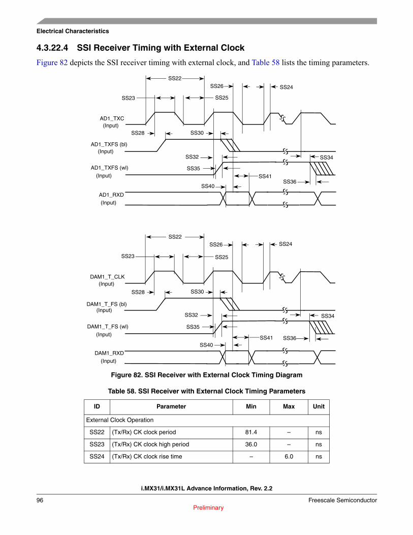
i.MX31/i.MX31L Advance Information, Rev. 2.2
96 Freescale Semiconductor Preliminary
Electrical Characteristics
4.3.22.4 SSI Receiver Timing with External Clock
Figure 82 depicts the SSI receiver timing with external clock, and Table 58 lists the timing parameters.
Figure 82. SSI Receiver with External Clock Timing Diagram
Table 58. SSI Receiver with External Clock Timing Parameters
ID Parameter Min Max Unit
External Clock Operation
SS22 (Tx/Rx) CK clock period 81.4 – ns
SS23 (Tx/Rx) CK clock high period 36.0 – ns
SS24 (Tx/Rx) CK clock rise time – 6.0 ns
SS24
SS34
SS35
SS30SS28
SS26
SS25SS23
AD1_TXC
AD1_TXFS (bl)
AD1_TXFS (wl)
AD1_RXD
SS40
SS22
SS32
SS36SS41
(Input)
(Input)
(Input)
(Input)
SS24
SS34
SS35
SS30SS28
SS26
SS25SS23
DAM1_T_CLK
DAM1_T_FS (bl)
DAM1_T_FS (wl)
DAM1_RXD
SS40
SS22
SS32
SS36SS41
(Input)
(Input)
(Input)
(Input)

Electrical Characteristics
i.MX31/i.MX31L Advance Information, Rev. 2.2
Freescale Semiconductor 97 Preliminary
4.3.23 USB Electrical Specifications
This section describes the electrical information of the USBOTG port. The OTG port supports both serial and parallel interfaces.
The high speed (HS) interface is supported via the ULPI (Ultra Low Pin Count Interface). Figure 83 depicts the USB ULPI timing diagram, and Table 59 lists the timing parameters.
Figure 83. USB ULPI Interface Timing Diagram
SS25 (Tx/Rx) CK clock low period 36.0 – ns
SS26 (Tx/Rx) CK clock fall time – 6.0 ns
SS28 (Rx) CK high to FS (bl) high -10.0 15.0 ns
SS30 (Rx) CK high to FS (bl) low 10.0 – ns
SS32 (Rx) CK high to FS (wl) high -10.0 15.0 ns
SS34 (Rx) CK high to FS (wl) low 10.0 – ns
SS35 (Tx/Rx) External FS rise time – 6.0 ns
SS36 (Tx/Rx) External FS fall time – 6.0 ns
SS40 SRXD setup time before (Rx) CK low 10.0 – ns
SS41 SRXD hold time after (Rx) CK low 2.0 – ns
Table 58. SSI Receiver with External Clock Timing Parameters (continued)
ID Parameter Min Max Unit
Clock
Control out (stp)
Data out
Control in (dir, nxt)
Data in
TDD
TDC TDC
TSC
TSD THD
THC

i.MX31/i.MX31L Advance Information, Rev. 2.2
98 Freescale Semiconductor Preliminary
Package Information and Pinout
5 Package Information and PinoutThis section includes the following:
• Pin/contact assignment information• Mechanical package drawing
5.1 MAPBGA Production Package 457 14 x 14 mm, 0.5 PitchSee Figure 84 for package drawings and dimensions of the production package.
Table 59. USB ULPI Interface Timing Specification1
1 Timing parameters are given as viewed by transceiver side.
Parameter Symbol Min Max Units
Setup time (control in, 8-bit data in) TSC, TSD 6 – ns
Hold time (control in, 8-bit data in) THC, THD 0 – ns
Output delay (control out, 8-bit data out) TDC, TDD – 9 ns

Package Information and Pinout
i.MX31/i.MX31L Advance Information, Rev. 2.2
Freescale Semiconductor 99 Preliminary
5.1.1 Production Package Outline Drawing
Figure 84. Production Package: Mechanical Drawing

i.MX
31/i.MX
31L A
dvance In
form
ation
, Rev. 2.2
100Freescale S
emiconductor
Prelim
inary
Packag
e Info
rmatio
n an
d P
ino
ut
5.1.2 MAPBGA Signal Assignment
Figure 85. i.MX31/i.MX31L Ball Map
1 2 3 4 5 6 7 8 9 10 11 12 13 14 15 16 17 18 19 20 21 22 23 24 25 26
A GND GND SFS5 CSPI2_MISO
CSPI2_SS2
USBOTG_DATA7
USBOTG_DATA3
USBOTG_NXT
USB_BYP
RXD1 DSR_DCE1
DSR_DTE1
RXD2 CE_CONTROL
KEY_ROW3
KEY_ROW7
KEY_COL3
KEY_COL7
TDO SJC_MOD
SVEN0 CAPTURE
GPIO1_6
WATCHDOG_RST
GND GND A
B GND GND STXD4 SRXD5
CSPI2_SS0
CSPI2_SPI_RDY
USBOTG_DATA5
USBOTG_DATA1
USBOTG_DIR
USB_PWR
CTS1 DCD_DCE1
DCD_DTE1
RTS2 KEY_ROW1
KEY_ROW5
KEY_COL1
KEY_COL5
TCK TRSTB SRX0 SCLK0 GPIO1_1
GPIO1_5
GND GND B
C GND GND SRXD4 SCK4 STXD5 CSPI2_SS1
CSPI2_SCLK
USBOTG_DATA4
USBOTG_STP
USB_OC
DTR_DCE1
DTR_DTE1
TXD2 KEY_ROW2
KEY_COL0
KEY_COL4
RTCK DE SRST0 GPIO1_2
BOOT_MODE1
BOOT_MODE3
CLKO GND GND GND C
D GND CSPI3_MOSI
SCK5 BOOT_MODE2
GND BOOT_MODE4
D
E CSPI3_SCLK
ATA_DIOR
CSPI2_MOSI
NVCC5 GND GND DVFS0 POWER_FAIL
E
F ATA_DMACK
ATA_CS1
SFS4 NVCC5 BATT_LINE
USBOTG_DATA6
USBOTG_DATA0
TXD1 RI_DCE1
DTR_DCE2
KEY_ROW0
KEY_ROW6
KEY_COL6
TDI STX0 GPIO1_0
GPIO1_4
BOOT_MODE0
GND CKIH GPIO1_3
VSTBY F
G PWMO PC_RW
CSPI3_MISO
CSPI3_SPI_RDY
NVCC5 USBOTG_DATA2
USBOTG_CLK
RTS1 RI_DTE1
CTS2 KEY_ROW4
KEY_COL2
TMS SIMPD0
COMPARE
NVCC1 NVCC1 DVFS1 VPG0 CLKSS G
H PC_RST
PC_BVD1
ATA_RESET
ATA_DIOW
CKIL POR I2C_DAT
GPIO3_1
H
J PC_VS1
PC_READY
IOIS16 ATA_CS0
PC_POE
QVCC1 QVCC1 NVCC8 NVCC8 QVCC NVCC6 NVCC6 NVCC9 VPG1 RESET_IN
I2C_CLK
CSI_VSYNC
CSI_PIXCLK
J
K PC_CD2
SD1_DATA3
PC_PWRON
PC_BVD2
PC_VS2
QVCC1 NVCC6 NVCC1 CSI_HSYNC
GPIO3_0
CSI_MCLK
CSI_D5 CSI_D7 K
L SD1_DATA1
SD1_CMD
SD1_DATA2
PC_WAIT
PC_CD1
NVCC3 QVCC1 GND QVCC QVCC QVCC QVCC NVCC4 NVCC4 CSI_D8 CSI_D4 CSI_D6 CSI_D9 CSI_D11
L
M USBH2_DATA0
USBH2_STP
USBH2_DATA1
SD1_DATA0
SD1_CLK
NVCC3 GND GND GND GND GND GND QVCC CSI_D14
CSI_D12
CSI_D10
CSI_D13
CSI_D15
M
N USBH2_CLK
CSPI1_SCLK
CSPI1_SPI_RDY
USBH2_NXT
USBH2_DIR
QVCC4 NVCC3 GND GND GND GND GND NVCC7 SD_D_I FPSHIFT
VSYNC0
HSYNC DRDY0 N
P CSPI1_SS1
CSPI1_MOSI
CSPI1_SS0
CSPI1_SS2
CSPI1_MISO
NVCC10
NVCC10
GND GND GND GND GND NVCC7 READ LCS1 SD_D_CLK
SD_D_IO
LCS0 P
R STXD3 SCK3 SRXD3 SFS3 SRXD6 QVCC4 NVCC10
GND GND GND GND GND NVCC7 D3_CLS
PAR_RS CONTRAST
WRITE VSYNC3
R
T STXD6 SCK6 SFS6 NFCE NFWE QVCC4 NVCC10
GND GND SGND MGND UGND NVCC7 LD4 LD2 LD0 SER_RS
D3_REV T
U NFRB NFWP NFCLE D15 D11 QVCC4 QVCC TTM_PAD
LD8 LD6 D3_SPL LD1 U
V NFALE NFRE D13 D9 D5 QVCC QVCC QVCC QVCC SVCC MVCC UVCC GND LD17 LD13 LD10 LD3 LD5 V
W D14 D12 D7 D3 NVCC22
EB0 LD15 LD7 LD9 W
Y D10 D8 D1 IOQVDD
NVCC22
NVCC22
NVCC22
NVCC22
NVCC22
NVCC22
NVCC22
NVCC21
NVCC21
NVCC21
NVCC2 NVCC2 NVCC2 NVCC2 M_GRANT
EB1 LD11 LD12 Y
AA D6 D4 A4 NVCC22
SD31 SD28 SD27 SD23 SD21 SD18 SD16 SD13 SD9 SD7 SD5 SD3 SD2 DQM2 SDCLK FVCC LD14 LD16 AA
AB D2 D0 A6 A2 RW FGND OE BCLK AB
AC MA10 GND A11 FUSE_VDD
M_REQUEST
GND AC
AD GND GND A12 A13 A8 A0 SDBA0 SDQS3 SD29 SD25 SDQS2 SD17 SD15 SD12 SD8 SDQS0 SD4 SD0 DQM1 CAS SDCKE0
CS3 ECB GND GND GND AD
AE GND GND A7 A3 SDBA1 SD30 SD26 SD24 SD22 SD20 SD19 SDQS1 SD14 SD11 SD10 SD6 SD1 DQM3 DQM0 SDCLK CS2 LBA CS0 GND GND GND AE
AF GND GND A9 A5 A1 A25 A24 A23 A22 A21 A20 A19 A18 A17 A16 A15 A14 A10 RAS SDWE SDCKE1
CS5 CS1 CS4 GND GND AF
1 2 3 4 5 6 7 8 9 10 11 12 13 14 15 16 17 18 19 20 21 22 23 24 25 26

Package Information and Pinout
i.MX31/i.MX31L Advance Information, Rev. 2.2
Freescale Semiconductor 101 Preliminary
Table 60 shows the device connection list for power and ground, alpha-sorted.Table 60. 14 x 14 BGA (Ground/Power ID by Ball Grid Location)
GND/PWR ID Ball Location
FGND AB24
FUSE_VDD AC24
FVCC AA24GND A1, A2, A25, A26, B1, B2, B25, B26, C1, C2, C24, C25, C26, D1, D25, E22, E24, F21, L12, M11, M12, M13, M14,
M15, M16, N12, N13, N14, N15, N16, P12, P13, P14, P15, P16, R12, R13, R14, R15, R16, T12, T13, V17, AC2, AC26, AD1, AD2, AD24, AD25, AD26, AE1, AE2, AE24, AE25, AE26, AF1, AF2, AF25, AF26
IOQVDD Y6MGND T15
MVCC V15
NVCC1 G19, G21, K18NVCC2 Y17, Y18, Y19, Y20
NVCC3 L9, M9, N11
NVCC4 L18, L19NVCC5 E5, F6, G7
NVCC6 J15, J16, K15
NVCC7 N18, P18, R18, T18NVCC8 J12, J13
NVCC9 J17
NVCC10 P9, P11, R11, T11NVCC21 Y14, Y15, Y16
NVCC22 W7, Y7, Y8, Y9, Y10, Y11, Y12, Y13, AA6
QVCC J14, L13, L14, L15, L16, M18, U18, V10, V11, V12, V13QVCC1 J10, J11, K9, L11
QVCC4 N9, R9, T9, U9
SGND T14SVCC V14
UVCC V16
UGND T16

i.MX31/i.MX31L Advance Information, Rev. 2.2
102 Freescale Semiconductor Preliminary
Package Information and Pinout
Table 61 shows the device connection list for signals only, alpha-sorted by signal identification.Table 61. 14 x 14 BGA (Signal ID by Ball Grid Location)
Signal ID Ball Location Signal ID Ball Location
A0 AD6 CKIL H21
A1 AF5 CLKO C23
A10 AF18 CLKSS G26A11 AC3 COMPARE G18
A12 AD3 CONTRAST R24
A13 AD4 CS0 AE23A14 AF17 CS1 AF23
A15 AF16 CS2 AE21
A16 AF15 CS3 AD22A17 AF14 CS4 AF24
A18 AF13 CS5 AF22
A19 AF12 CSI_D10 M24A2 AB5 CSI_D11 L26
A20 AF11 CSI_D12 M21
A21 AF10 CSI_D13 M25A22 AF9 CSI_D14 M20
A23 AF8 CSI_D15 M26
A24 AF7 CSI_D4 L21A25 AF6 CSI_D5 K25
A3 AE4 CSI_D6 L24
A4 AA3 CSI_D7 K26A5 AF4 CSI_D8 L20
A6 AB3 CSI_D9 L25
A7 AE3 CSI_HSYNC K20A8 AD5 CSI_MCLK K24
A9 AF3 CSI_PIXCLK J26
ATA_CS0 J6 CSI_VSYNC J25ATA_CS1 F2 CSPI1_MISO P7
ATA_DIOR E2 CSPI1_MOSI P2
ATA_DIOW H6 CSPI1_SCLK N2ATA_DMACK F1 CSPI1_SPI_RDY N3
ATA_RESET H3 CSPI1_SS0 P3
BATT_LINE F7 CSPI1_SS1 P1BCLK AB26 CSPI1_SS2 P6
BOOT_MODE0 F20 CSPI2_MISO A4
BOOT_MODE1 C21 CSPI2_MOSI E3BOOT_MODE2 D24 CSPI2_SCLK C7
BOOT_MODE3 C22 CSPI2_SPI_RDY B6
BOOT_MODE4 D26 CSPI2_SS0 B5CAPTURE A22 CSPI2_SS1 C6
CAS AD20 CSPI2_SS2 A5
CE_CONTROL A14 CSPI3_MISO G3
CKIH F24 CSPI3_MOSI D2
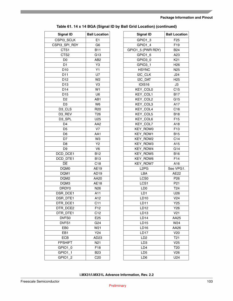
Package Information and Pinout
i.MX31/i.MX31L Advance Information, Rev. 2.2
Freescale Semiconductor 103 Preliminary
CSPI3_SCLK E1 GPIO1_3 F25CSPI3_SPI_RDY G6 GPIO1_4 F19
CTS1 B11 GPIO1_5 (PWR RDY) B24
CTS2 G13 GPIO1_6 A23
D0 AB2 GPIO3_0 K21D1 Y3 GPIO3_1 H26
D10 Y1 HSYNC N25
D11 U7 I2C_CLK J24D12 W2 I2C_DAT H25
D13 V3 IOIS16 J3
D14 W1 KEY_COL0 C15D15 U6 KEY_COL1 B17
D2 AB1 KEY_COL2 G15
D3 W6 KEY_COL3 A17D3_CLS R20 KEY_COL4 C16
D3_REV T26 KEY_COL5 B18
D3_SPL U25 KEY_COL6 F15D4 AA2 KEY_COL7 A18
D5 V7 KEY_ROW0 F13
D6 AA1 KEY_ROW1 B15D7 W3 KEY_ROW2 C14
D8 Y2 KEY_ROW3 A15
D9 V6 KEY_ROW4 G14DCD_DCE1 B12 KEY_ROW5 B16
DCD_DTE1 B13 KEY_ROW6 F14
DE C18 KEY_ROW7 A16DQM0 AE19 L2PG See VPG1.
DQM1 AD19 LBA AE22
DQM2 AA20 LCS0 P26DQM3 AE18 LCS1 P21
DRDY0 N26 LD0 T24
DSR_DCE1 A11 LD1 U26DSR_DTE1 A12 LD10 V24
DTR_DCE1 C11 LD11 Y25
DTR_DCE2 F12 LD12 Y26DTR_DTE1 C12 LD13 V21
DVFS0 E25 LD14 AA25
DVFS1 G24 LD15 W24EB0 W21 LD16 AA26
EB1 Y24 LD17 V20
ECB AD23 LD2 T21FPSHIFT N21 LD3 V25
GPIO1_0 F18 LD4 T20
GPIO1_1 B23 LD5 V26
GPIO1_2 C20 LD6 U24
Table 61. 14 x 14 BGA (Signal ID by Ball Grid Location) (continued)
Signal ID Ball Location Signal ID Ball Location

i.MX31/i.MX31L Advance Information, Rev. 2.2
104 Freescale Semiconductor Preliminary
Package Information and Pinout
LD7 W25 SCK6 T2LD8 U21 SCLK0 B22
LD9 W26 SD_D_CLK P24
M_GRANT Y21 SD_D_I N20
M_REQUEST AC25 SD_D_IO P25MA10 AC1 SD0 AD18
MCUPG See VPG0. SD1 AE17
NFALE V1 SD1_CLK M7NFCE T6 SD1_CMD L2
NFCLE U3 SD1_DATA0 M6
NFRB U1 SD1_DATA1 L1NFRE V2 SD1_DATA2 L3
NFWE T7 SD1_DATA3 K2
NFWP U2 SD10 AE15OE AB25 SD11 AE14
PAR_RS R21 SD12 AD14
PC_BVD1 H2 SD13 AA14PC_BVD2 K6 SD14 AE13
PC_CD1 L7 SD15 AD13
PC_CD2 K1 SD16 AA13PC_POE J7 SD17 AD12
PC_PWRON K3 SD18 AA12
PC_READY J2 SD19 AE11PC_RST H1 SD2 AA19
PC_RW G2 SD20 AE10
PC_VS1 J1 SD21 AA11PC_VS2 K7 SD22 AE9
PC_WAIT L6 SD23 AA10
POR H24 SD24 AE8POWER_FAIL E26 SD25 AD10
PWMO G1 SD26 AE7
RAS AF19 SD27 AA9READ P20 SD28 AA8
RESET_IN J21 SD29 AD9
RI_DCE1 F11 SD3 AA18RI_DTE1 G12 SD30 AE6
RTCK C17 SD31 AA7
RTS1 G11 SD4 AD17RTS2 B14 SD5 AA17
RW AB22 SD6 AE16
RXD1 A10 SD7 AA16RXD2 A13 SD8 AD15
SCK3 R2 SD9 AA15
SCK4 C4 SDBA0 AD7
SCK5 D3 SDBA1 AE5
Table 61. 14 x 14 BGA (Signal ID by Ball Grid Location) (continued)
Signal ID Ball Location Signal ID Ball Location

Product Documentation
i.MX31/i.MX31L Advance Information, Rev. 2.2
Freescale Semiconductor 105 Preliminary
6 Product DocumentationThis Data Sheet is labeled as a particular type: Product Preview, Advance Information, or Technical Data. Definitions of these types are available at: http://www.freescale.com.
All related product documentation for the i.MX31 and i.MX31L is located at http://www.freescale.com\imx.
SDCKE0 AD21 TRSTB B20SDCKE1 AF21 TTM_PAD U20
SDCLK AA21 TXD1 F10
SDCLK AE20 TXD2 C13
SDQS0 AD16 USB_BYP A9SDQS1 AE12 USB_OC C10
SDQS2 AD11 USB_PWR B10
SDQS3 AD8 USBH2_CLK N1SDWE AF20 USBH2_DATA0 M1
SER_RS T25 USBH2_DATA1 M3
SFS3 R6 USBH2_DIR N7SFS4 F3 USBH2_NXT N6
SFS5 A3 USBH2_STP M2
SFS6 T3 USBOTG_CLK G10SIMPD0 G17 USBOTG_DATA0 F9
SJC_MOD A20 USBOTG_DATA1 B8
SRST0 C19 USBOTG_DATA2 G9SRX0 B21 USBOTG_DATA3 A7
SRXD3 R3 USBOTG_DATA4 C8
SRXD4 C3 USBOTG_DATA5 B7SRXD5 B4 USBOTG_DATA6 F8
SRXD6 R7 USBOTG_DATA7 A6
STX0 F17 USBOTG_DIR B9STXD3 R1 USBOTG_NXT A8
STXD4 B3 USBOTG_STP C9
STXD5 C5 VPG0 G25STXD6 T1 VPG1 J20
SVEN0 A21 VSTBY F26
TCK B19 VSYNC0 N24TDI F16 VSYNC3 R26
TDO A19 WATCHDOG_RST A24
TMS G16 WRITE R25
Table 61. 14 x 14 BGA (Signal ID by Ball Grid Location) (continued)
Signal ID Ball Location Signal ID Ball Location

i.MX31/i.MX31L Advance Information, Rev. 2.2
106 Freescale Semiconductor Preliminary
Product Documentation
6.1 Revision HistoryTable 62 summarizes revisions to this document since the release of Rev. 2.
Table 62. Revision History
Rev Location Revision
2.1 Table 28, "WEIM Bus Timing Parameters," on page 35
Changed WEIM Bus timing parameters for:WE14: Max value - from 10, to 13ns. WE15, FCE=1: Range min max from: -2 to 10ns, to 0 to 6ns. WE17, FCE=1: Range min max from: -2 to 10ns, to 0 to 6ns. WE16, FCE=1: Range min, max from: -7 to 0ns, to -3 to 2ns. WE18, FCE=1: Range min, max from: -7 to 0ns, to -3 to 2ns.
2.1 Table 59, "USB ULPI Interface Timing Specification," on page 98
USB ULPI Interface Timing Specification changed the third row value of Output delay (control out, 8-bit data out) from 9.0 in the Min column, to the Max column.
2.1 Table 6, "Recommended Operating Conditions," on page 11
Differentiated between overdrive and non-ovedrive values. Added values per these distinctions. Clarified table footnotes.
2.1 Table 8, "Current Consumption,," on page 13
Changed table name from Power Consumption to Current Consumption. Added Typical and Maximum columns and their values.
2.1 Section 3, “Signal Descriptions” Added Special Signal Considerations.
2.1 Table 1 on page 3, Ordering information Moved Ordering Information to table within text flow and added new available devices and footnotes.
2.1 Table 5, "Absolute Maximum Ratings," on page 10
Added HBM, MM, and CDM values separately within the ESD data. Changed HBM from 2500V to 2000V
2.1 Table 27, "NFC Timing Parameters," on page 33
Change NF16 and NF17 values in the NFC Timing Parameters table.
2.1 Figure 70, "SDHC Timing Diagram," on page 83 and Table 51, "SDHC Interface Timing Parameters," on page 83
Replaced SDHC Timing Diagram and modified SD 6–8 parameters.
2.1 Table 19, "ATA Timing Parameters," on page 21
Separated values for ti_ds and ti_dh for each UDMA.
2.2 Was Figure 3, “Power-Up Sequence Option 2,” on page 16
Deleted Figure 3, Power-Up Sequence, Option 2Removed “Option 1” from Figure 2.
2.2 Figure 2, "Power-Up Sequence," on page 15
Added Figure Footnote 4 regarding FUSE_VDD.
2.2 Table 28, "WEIM Bus Timing Parameters," on page 35
Changed WEIM13/14 min/max parameter values.
2.2 Table 26, "DPLL Specifications," on page 31
Added PLL output frequency range parameters.
2.2 Table 51, "SDHC Interface Timing Parameters," on page 83
Revised maximum parameter values for SD7/8.
2.2 Table 6, "Recommended Operating Conditions," on page 11
Changed the following parameter values: • Core operating voltage • PLL/FPM operating voltage • Modified footnotes 2 and 6.

i.MX31/i.MX31L Advance Information, Rev. 2.2
Freescale Semiconductor 107 Preliminary
NOTES

Document Number: MCIMX31Rev. 2.212/2006
Preliminary
How to Reach Us:
Home Page:www.freescale.com
E-mail:[email protected]
USA/Europe or Locations Not Listed:Freescale SemiconductorTechnical Information Center, CH3701300 N. Alma School RoadChandler, Arizona 85224+1-800-521-6274 or [email protected]
Europe, Middle East, and Africa:Freescale Halbleiter Deutschland GmbHTechnical Information CenterSchatzbogen 781829 Muenchen, Germany+44 1296 380 456 (English)+46 8 52200080 (English)+49 89 92103 559 (German)+33 1 69 35 48 48 (French)[email protected]
Japan:Freescale Semiconductor Japan Ltd.HeadquartersARCO Tower 15F1-8-1, Shimo-Meguro, Meguro-ku,Tokyo 153-0064, Japan0120 191014 or +81 3 5437 [email protected]
Asia/Pacific:Freescale Semiconductor Hong Kong Ltd.Technical Information Center2 Dai King StreetTai Po Industrial EstateTai Po, N.T., Hong Kong+800 2666 [email protected]
For Literature Requests Only:Freescale Semiconductor Literature Distribution CenterP.O. Box 5405Denver, Colorado 802171-800-521-6274 or 303-675-2140Fax: [email protected]
Information in this document is provided solely to enable system and software implementers to use Freescale Semiconductor products. There are no express or implied copyright licenses granted hereunder to design or fabricate any integrated circuits or integrated circuits based on the information in this document.
Freescale Semiconductor reserves the right to make changes without further notice to any products herein. Freescale Semiconductor makes no warranty, representation or guarantee regarding the suitability of its products for any particular purpose, nor does Freescale Semiconductor assume any liability arising out of the application or use of any product or circuit, and specifically disclaims any and all liability, including without limitation consequential or incidental damages. “Typical” parameters that may be provided in Freescale Semiconductor data sheets and/or specifications can and do vary in different applications and actual performance may vary over time. All operating parameters, including “Typicals”, must be validated for each customer application by customer’s technical experts. Freescale Semiconductor does not convey any license under its patent rights nor the rights of others. Freescale Semiconductor products are not designed, intended, or authorized for use as components in systems intended for surgical implant into the body, or other applications intended to support or sustain life, or for any other application in which the failure of the Freescale Semiconductor product could create a situation where personal injury or death may occur. Should Buyer purchase or use Freescale Semiconductor products for any such unintended or unauthorized application, Buyer shall indemnify and hold Freescale Semiconductor and its officers, employees, subsidiaries, affiliates, and distributors harmless against all claims, costs, damages, and expenses, and reasonable attorney fees arising out of, directly or indirectly, any claim of personal injury or death associated with such unintended or unauthorized use, even if such claim alleges that Freescale Semiconductor was negligent regarding the design or manufacture of the part.
Freescale™ and the Freescale logo are trademarks of Freescale Semiconductor, Inc. ARM, ARM Thumb, Jazelle, and the ARM Powered logo are registered trademarks of ARM Limited. ARM1136JF-S, ARM11, Embedded Trace Kit, Embedded Trace Macrocell, ETM, Embedded Trace Buffer, and ETB are trademarks of ARM Limited. All other product or service names are the property of their respective owners. Java and all other Java-based marks are trademarks or registered trademarks of Sun Microsystems, Inc. in the U.S. and other countries. France Telecom – TDF – Groupe des ecoles des telecommunications Turbo codes patents license.
© Freescale Semiconductor, Inc. 2005, 2006. All rights reserved.

专注于微波、射频、天线设计人才的培养 易迪拓培训 网址:http://www.edatop.com
射 频 和 天 线 设 计 培 训 课 程 推 荐
易迪拓培训(www.edatop.com)由数名来自于研发第一线的资深工程师发起成立,致力并专注于微
波、射频、天线设计研发人才的培养;我们于 2006 年整合合并微波 EDA 网(www.mweda.com),现
已发展成为国内最大的微波射频和天线设计人才培养基地,成功推出多套微波射频以及天线设计经典
培训课程和 ADS、HFSS 等专业软件使用培训课程,广受客户好评;并先后与人民邮电出版社、电子
工业出版社合作出版了多本专业图书,帮助数万名工程师提升了专业技术能力。客户遍布中兴通讯、
研通高频、埃威航电、国人通信等多家国内知名公司,以及台湾工业技术研究院、永业科技、全一电
子等多家台湾地区企业。
易迪拓培训课程列表:http://www.edatop.com/peixun/rfe/129.html
射频工程师养成培训课程套装
该套装精选了射频专业基础培训课程、射频仿真设计培训课程和射频电
路测量培训课程三个类别共 30 门视频培训课程和 3 本图书教材;旨在
引领学员全面学习一个射频工程师需要熟悉、理解和掌握的专业知识和
研发设计能力。通过套装的学习,能够让学员完全达到和胜任一个合格
的射频工程师的要求…
课程网址:http://www.edatop.com/peixun/rfe/110.html
ADS 学习培训课程套装
该套装是迄今国内最全面、最权威的 ADS 培训教程,共包含 10 门 ADS
学习培训课程。课程是由具有多年 ADS 使用经验的微波射频与通信系
统设计领域资深专家讲解,并多结合设计实例,由浅入深、详细而又
全面地讲解了 ADS 在微波射频电路设计、通信系统设计和电磁仿真设
计方面的内容。能让您在最短的时间内学会使用 ADS,迅速提升个人技
术能力,把 ADS 真正应用到实际研发工作中去,成为 ADS 设计专家...
课程网址: http://www.edatop.com/peixun/ads/13.html
HFSS 学习培训课程套装
该套课程套装包含了本站全部 HFSS 培训课程,是迄今国内最全面、最
专业的HFSS培训教程套装,可以帮助您从零开始,全面深入学习HFSS
的各项功能和在多个方面的工程应用。购买套装,更可超值赠送 3 个月
免费学习答疑,随时解答您学习过程中遇到的棘手问题,让您的 HFSS
学习更加轻松顺畅…
课程网址:http://www.edatop.com/peixun/hfss/11.html
`

专注于微波、射频、天线设计人才的培养 易迪拓培训 网址:http://www.edatop.com
CST 学习培训课程套装
该培训套装由易迪拓培训联合微波 EDA 网共同推出,是最全面、系统、
专业的 CST 微波工作室培训课程套装,所有课程都由经验丰富的专家授
课,视频教学,可以帮助您从零开始,全面系统地学习 CST 微波工作的
各项功能及其在微波射频、天线设计等领域的设计应用。且购买该套装,
还可超值赠送 3 个月免费学习答疑…
课程网址:http://www.edatop.com/peixun/cst/24.html
HFSS 天线设计培训课程套装
套装包含 6 门视频课程和 1 本图书,课程从基础讲起,内容由浅入深,
理论介绍和实际操作讲解相结合,全面系统的讲解了 HFSS 天线设计的
全过程。是国内最全面、最专业的 HFSS 天线设计课程,可以帮助您快
速学习掌握如何使用 HFSS 设计天线,让天线设计不再难…
课程网址:http://www.edatop.com/peixun/hfss/122.html
13.56MHz NFC/RFID 线圈天线设计培训课程套装
套装包含 4 门视频培训课程,培训将 13.56MHz 线圈天线设计原理和仿
真设计实践相结合,全面系统地讲解了 13.56MHz线圈天线的工作原理、
设计方法、设计考量以及使用 HFSS 和 CST 仿真分析线圈天线的具体
操作,同时还介绍了 13.56MHz 线圈天线匹配电路的设计和调试。通过
该套课程的学习,可以帮助您快速学习掌握 13.56MHz 线圈天线及其匹
配电路的原理、设计和调试…
详情浏览:http://www.edatop.com/peixun/antenna/116.html
我们的课程优势:
※ 成立于 2004 年,10 多年丰富的行业经验,
※ 一直致力并专注于微波射频和天线设计工程师的培养,更了解该行业对人才的要求
※ 经验丰富的一线资深工程师讲授,结合实际工程案例,直观、实用、易学
联系我们:
※ 易迪拓培训官网:http://www.edatop.com
※ 微波 EDA 网:http://www.mweda.com
※ 官方淘宝店:http://shop36920890.taobao.com
专注于微波、射频、天线设计人才的培养
官方网址:http://www.edatop.com 易迪拓培训 淘宝网店:http://shop36920890.taobao.com