Embed Size (px)
Citation preview

Document Number: 79076Rev. 3.0, 3/2007
Freescale Semiconductor Technical Data
Electronic Ignition Control Circuit
The 79076, in conjunction with an appropriate Freescale Power Darlington Transistor, provides an economical solution for automotive ignition applications. The 79076 offers optimum performance by providing closed loop operation of the Power Darlington in controlling the ignition coil current.
Features• Hall or Variable Reluctance Sensor Input• Ignition Coil Voltage Internally Limited to 375 V• Coil Current Limiting to 7.5 A• Output On–Time (Dwell) Control• Dwell Feedback Control to Sense Coil Variation• Pb-Free Packaging Designated by Suffix Code EG
Figure 1. 79076 Simplified Application Diagram
ELECTRONIC IGNITION CONTROL CIRCUIT
DW SUFFIXEG (PB-FREE) SUFFIX
98ASB42567B16-PIN SOIC
79076
ORDERING INFORMATION
Device Temperature Range (TA) Package
MC79076DW/R2-30°C to 125°C 16 SOIC
MCZ79076EG/R2
79076POWER GROUND
CURRENT SENSE
DWELL
VCC
SIGNAL GROUNDREFERENCE/DWELL
ADVANCE
BIAS VOLTAGEEST
REFERENCEBYPASS
DWELL CONTROL
RPM DETECT
Freescale Semiconductor, Inc. reserves the right to change the detail specifications, as may be required, to permit improvements in the design of its products. © Freescale Semiconductor, Inc., 2007. All rights reserved.

INTERNAL BLOCK DIAGRAM
INTERNAL BLOCK DIAGRAM
Figure 2. 79076 Simplified Internal Block Diagram
ReferenceGenerator
Logicand
Control
Output
POWER GROUND
CURRENT SENSE
DWELL
VCC
SIGNAL GROUNDREFERENCE/DWELL
ADVANCE
BIAS VOLTAGE
REFERENCEBYPASS
DWELL CONTROL
RPM DETECT
EST
Analog Integrated Circuit Device Data 2 Freescale Semiconductor
79076

PIN CONNECTIONS
PIN CONNECTIONS
Figure 3. 79076 Pin Connections
1
23
456
7
8 9
10
11
12
13
14
15
16Power Ground
Current Sense
Dwell
VCC
Signal Ground
Reference/Dwell
Advance
Bias Voltage EST
Reference
Bypass
RPM Detect
Dwell Control
NC
NC
NC
Analog Integrated Circuit Device Data Freescale Semiconductor 3
79076

ELECTRICAL CHARACTERISTICSMAXIMUM RATINGS
ELECTRICAL CHARACTERISTICS
MAXIMUM RATINGS
Table 1. Maximum Ratings
All voltages are with respect to ground unless otherwise noted. Exceeding these ratings may cause a malfunction or permanent damage to the device.
Ratings Symbol Value Unit
ELECTRICAL RATINGS
Supply VoltageSteady-State Transient Conditions (1)
VCC(SUS)
VCC(PK)
3650
V
Supply Current
Transient Conditions (2) Transient Negative Current (tT = 60ms) Transient Negative Current (tT = 1ms)
IT1.0
-100-1.3
AmAA
Input Voltage (3)
Ref/Dwell, Advance EST, Bypass
VIN1
VIN2
-5.0 to 30-5.0 to 24
V
Ref/Dwell Input Current IIN1 -20 mA
Dwell ON Sink CurrentOutput ON (Operating) Output ON (t = 10ms)
ID0.30.8
A
Dwell OFF Voltage (4) VD(OFF) 5.0 V
THERMAL RATINGS
Storage Temperature TSTG -65 to 150 °C
Operating Ambient Temperature TA -30 to 125 °C
THERMAL RESISTANCE
Operating Junction Temperature TJ -30 to 150 °C
Thermal Resistance (Junction-to-Ambient) - SO8 ØJ-A 80 °C/W
Peak Package Reflow Temperature During Reflow (5), (6) TPPRT Note 6 °C
Notes1. Survivability of device with transient voltage applied to VCC pin for a duration not to exceed 10ms.2. Survivability of device with overvoltage applied to VCC pin producing the current for a duration not to exceed 10ms.3. Exceeding this voltage range on the function pin may cause permanent damage to the device.4. A zener diode is incorporated across collector to emitter of the output NPN device to prevent voltage overdrive of the external Darlington
switch transistor.5. Pin soldering temperature limit is for 10 seconds maximum duration. Not designed for immersion soldering. Exceeding these limits may
cause malfunction or permanent damage to the device.6. Freescale’s Package Reflow capability meets Pb-free requirements for JEDEC standard J-STD-020C. For Peak Package Reflow
Temperature and Moisture Sensitivity Levels (MSL), Go to www.freescale.com, search by part number [e.g. remove prefixes/suffixes and enter the core ID to view all orderable parts. (i.e. MC33xxxD enter 33xxx), and review parametrics.
Analog Integrated Circuit Device Data 4 Freescale Semiconductor
79076

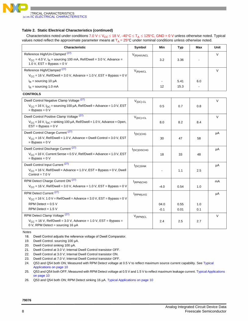
ELECTRICAL CHARACTERISTICSSTATIC ELECTRICAL CHARACTERISTICS
STATIC ELECTRICAL CHARACTERISTICS
Table 2. Static Electrical Characteristics Characteristics noted under conditions 7.0 V ≤ VCC ≤ 18 V, - 40°C ≤ TA ≤ 125°C, GND = 0 V unless otherwise noted. Typical
values noted reflect the approximate parameter means at TA = 25°C under nominal conditions unless otherwise noted.
Characteristic Symbol Min Typ Max Unit
INPUTS
Advance Input Resistance (VCC = 16 V, Ref/Dwell = 1.0 V, Advance = 1.0 mA, EST = Bypass = 0 V)
R(A)
15 18 25kΩ
Advance Voltage (7)
VCC = 16 V, Ref/Dwell = 1.0 V, EST = Bypass = 0 VVTH(A)
- 0.05 0.1V
Advance Threshold Voltage (7)
(VCC = 16 V, Ref/Dwell = 1.0 V, EST = Bypass = 0 V,)
Dwell = Reference = RPM Detect = open, Dwell Control = sinking 10 µA)IncreasingDecreasingHysteresis
VTH+(A)
VTH-(A)
VHYS(A)
VB + 0.103VB + 0.045
0.018
VB + 0.114VB + 0.068
0.045
VB + 0.130--
V
Bypass Input Resistance (VCC = 16 V, Ref/Dwell = Advance = 3.0 V, EST = Bypass = 0 V)
R(BP) 6.0 9.2 16 kΩ
Bypass Voltage (VCC = 16 V, Ref/Dwell = Advance = 1.0 V, EST = 0V)
V(BP) - 0.065 0.1 V
Bypass Threshold Voltage (8)
(Ref/Dwell = Advance = 1.0 V, EST = 3.0 V)IncreasingDecreasingHysteresis
VTH+(BP)
VTH-(BP)
VHYS(BP)
VB + 1.6VB + 0.9
0.65
VB + 0.188VB + 0.103
0.86
VB + 2.1--
V
Current Sense Threshold Voltage (9)
(VCC = 16 V, Ref/Dwell = Advance = 1.0 V, EST = Bypass = 3.0 V)VTH(CS)
90 105 121mV
EST Input Resistance(VCC = 16 V, Ref/Dwell = Advance = 1.0 V, Bypass = 3.0 V)
R(EST)
7.0 10.3 18kΩ
EST Input Voltage (EST Mode) (VCC = 16 V, Ref/Dwell = Advance = 1.0 V, Bypass = 3.0 V)
V(EST)
- 0.070.1 V
Notes7. Advance Threshold Voltage is the positive (or negative) going voltage on Advance necessary cause the Dwell Control voltage to positive
(or negative) going transition 2.0 V respectively. It is expressed as VTH±(A) = VB + VX where VB is the Bias Voltage and VX is the additional voltage necessary to attain the threshold.
8. Bypass Threshold Voltage is the positive (or negative) going voltage on Bypass necessary cause the Dwell voltage to positive (or negative) going transition 1.5 V respectively. It is expressed as VTH±(BP) = VB + VX where VB is the Bias Voltage and VX is the additional voltage necessary to attain the threshold.
9. Increasing voltage on Current Sense which when attained will cause Dwell to transition low to 1.5 V with a 10 mA load.
Analog Integrated Circuit Device Data Freescale Semiconductor 5
79076

ELECTRICAL CHARACTERISTICSSTATIC ELECTRICAL CHARACTERISTICS
EST Threshold Voltage (10)
(Ref/Dwell = Advance = 1.0 V, Bypass = 3.0 V)IncreasingDecreasingHysteresis
VTH+(EST)
VTH-(EST)
VHYS(EST)
1.650.8
0.79
1.860.890.97
2.0--
V
Ref/Dwell Current (11)
(VCC = 16 V, Advance = 1.0 V, EST = Bypass = 0 V)
Ref/Dwell Voltage = 1.0 VRef/Dwell Voltage = 20 V
I(R/D)
-12-1.0
-1.380.02
1.05.0
µA
Ref/Dwell Clamp Voltage (VCC = 16 V, Advance = 1.0 V, EST = Bypass = 0 V)
IR/D = 100µA (Sourcing)
IR/D = 1.0mA (Sourcing)
V(R/D)CL
-0.01-0.62
-0.04-0.54
0.2-
V
Ref/Dwell Threshold (Bypass Mode) (12)
(Advance = 1.0 V, EST = Bypass = 0 V, Reference = sinking 10 µA)IncreasingDecreasingHysteresis
VTH+(R/D)BP
VTH-(R/D)BP
VHYS(R/D)BP
VB + 0.09VB + 0.018
0.055
VB + 0.106VB + 0.03
0.076
VB + 0.116--
V
Ref/Dwell Threshold (EST Mode) (12)
(Advance = 1.0 V, EST = 0 V, Bypass = 3.0 V, Reference = sinking 10 µA)IncreasingDecreasingHysteresis
VTH+(R/D)EST
VTH-(R/D)EST
VHYS(R/D)EST
VB + 0.445VB + 0.038
0.395
VB + 0.50VB + 0.062
0.436
VB + 0.535--
V
Ref/Dwell Threshold (No Pump) (13)
(Advance = 1.0 V, EST = Bypass = 0 V, Dwell = sinking 10 mA)IncreasingDecreasingHysteresis
VTH+(R/D)NP
VTH-(R/D)NP
VHYS(R/D)NP
VB + 0.003VB + 0.021VB + 0.013
VB + 0.118VB + 0.047VB + 0.072
VB + 0.128--
V
Notes10. EST Threshold Voltage is the positive (or negative) going voltage on EST necessary cause the Dwell voltage to positive (or negative)
going transition 1.5 V respectively. It is expressed as VTH±(EST) and is in reference to ground.11. Ref/Dwell can either source or sink current; A minus sign denotes the Ref/Dwell is sourcing current.12. Ref/Dwell Threshold Voltage (Bypass Mode) is the positive (or negative) going voltage on Ref/Dwell necessary cause the Reference
voltage to positive (or negative) going transition 1.5 V respectively. It is expressed as VTH±(RD) = VB + VX where VB is the Bias Voltage and VX is the additional voltage necessary to attain the threshold.
13. Ref/Dwell Threshold Voltage (No Pump) is the positive (or negative) going voltage on Ref/Dwell necessary cause the Dwell voltage to positive (or negative) going transition 1.5 V respectively. It is expressed as VTH±(RD) = VB + VX where VB is the Bias Voltage and VX is the additional voltage necessary to attain the threshold. Advance = 1.0 V providing no input assist or "No Pump" influence of Dwell signal; Reference open.
Table 2. Static Electrical Characteristics (continued)Characteristics noted under conditions 7.0 V ≤ VCC ≤ 18 V, - 40°C ≤ TA ≤ 125°C, GND = 0 V unless otherwise noted. Typical
values noted reflect the approximate parameter means at TA = 25°C under nominal conditions unless otherwise noted.
Characteristic Symbol Min Typ Max Unit
Analog Integrated Circuit Device Data 6 Freescale Semiconductor
79076

ELECTRICAL CHARACTERISTICSSTATIC ELECTRICAL CHARACTERISTICS
Ref/Dwell Threshold (Max Pump) (14)
(VCC = 16 V, Advance = 3.0 V, EST = Bypass = 0 V, Dwell sinking 10 mA, Dwell Control = open)IncreasingDecreasingHysteresis
VTH+(R/D)MP
VTH-(R/D)MP
VHYS(R/D)MP
VB + 0.175VB + 0.115VB + 0.025
VB + 0.474VB + 0.425VB + 0.048
VB + 0.80VB + 0.735
-
V
OUTPUTS
Bias Resistance to GroundDwell = VCC = Ref/Dwell = Reference = Dwell Control = open, Advance = 1.0 V, EST = Bypass = 0 V
R(B)
0.55 0.68 0.9kΩ
Bias Voltage (Bypass Mode)Ref/Dwell = Advance = 1.0 V, EST = Bypass = 0 V
V(B)BP
2.25 2.43 2.6V
Bias Voltage Regulation (Bypass Mode) Ref/Dwell = Advance = 1.0 V, EST = Bypass = 0 V
V(B)BP
- 30 40mV
Bias Voltage (EST Mode) VCC = 16 V, Ref/Dwell = Advance = 1.0 V, EST = 0 V, Bypass = 3.0 V
V(B)EST
1.9 2.04 2.2V
Dwell Saturation VoltageVCC = 4.0 V, ID = 40 mA, Ref/Dwell = Advance =3.0 V, EST = Bypass = 0 VVCC = 16 V, ID = 160 mA, Ref/Dwell = Advance =3.0 V, EST = Bypass = 0 VVCC = 24 V, ID = 240 mA, Ref/Dwell = Advance =1.0 V, EST = Bypass = 3.0 VVCC = 36 V, ID = 360 mA, Ref/Dwell = Advance =1.0 V, EST = Bypass = 3.0 V
V(D)SAT
-
-
-
-
0.05
0.14
0.20
0.29
0.1
0.24
0.35
0.5
V
Dwell Reverse Clamp Voltage (15) V(D)REV -0.9 -0.98 -1.2 V
Dwell Leakage Current (16)
VCC = 16 V, Dwell = 5.0 V, Ref/Dwell = Advance = 3.0 V, EST = Bypass = 0, Bias Voltage = Reference = open
I(D)KG
- 0.044 50µA
Reference Low (17)
IR = sinking 0.3 mA, Ref/Dwell = Advance = 1.0 V, EST = Bypass = 0 V
V(R)LOW
- 0.13 0.22V
Notes14. Ref/Dwell Threshold Voltage (Max Pump) is the positive (or negative) going voltage on Ref/Dwell necessary cause the Dwell voltage to
positive (or negative) going transition 1.5 V respectively. It is expressed as VTH±(RD) = VB + VX where VB is the Bias Voltage and VX is the additional voltage necessary to attain the threshold. Advance = 3.0 V providing maximum input assist or Max Pump" influence of Dwell signal; Reference = Dwell Control = open.
15. All pins open except Pwr Gnd with Dwell sinking 200 mA.16. Limit conditions with Dwell output NPN in the OFF condition.17. Reference saturation voltage to ground with 0.3mA of current going into the Reference.
Table 2. Static Electrical Characteristics (continued)Characteristics noted under conditions 7.0 V ≤ VCC ≤ 18 V, - 40°C ≤ TA ≤ 125°C, GND = 0 V unless otherwise noted. Typical
values noted reflect the approximate parameter means at TA = 25°C under nominal conditions unless otherwise noted.
Characteristic Symbol Min Typ Max Unit
Analog Integrated Circuit Device Data Freescale Semiconductor 7
79076
ELECTRICAL CHARACTERISTICSSTATIC ELECTRICAL CHARACTERISTICS
Reference High/Un-Clamped (27)
VCC = 4.0 V, IR = sourcing 100 mA, Ref/Dwell = 3.0 V, Advance = 1.0 V, EST = Bypass = 0 V
V(R)HI/UNCL
3.2 3.36 -V
Reference High/Clamped (27)
VCC = 16 V, Ref/Dwell = 3.0 V, Advance = 1.0 V, EST = Bypass = 0 V
IR = sourcing 10 µA
IR = sourcing 1.0 mA
V(R)HI/CL
-12
5.4115.3
6.0-
V
CONTROLS
Dwell Control Negative Clamp Voltage (27)
VCC = 16 V, IDC = sourcing 100 µA, Ref/Dwell = Advance = 1.0 V, EST = Bypass = 0 V
V(DC)-CL
0.5 0.7 0.8V
Dwell Control Positive Clamp Voltage (27)
VCC = 16 V, IDC = sinking 100 µA, Ref/Dwell = 1.0 V, Advance = Open, EST = Bypass = 0 V
V(DC)+CL
8.0 8.2 8.4V
Dwell Control Charge Current (27)
VCC = 16 V, Ref/Dwell = 1.0 V, Advance = Dwell Control = 3.0 V, EST = Bypass = 0 V
I(DC)CHG
30 47 58µA
Dwell Control Discharge Current (27)
VCC = 16 V, Current Sense = 0.5 V, Ref/Dwell = Advance = 1.0 V, EST = Bypass = 0 V
I(DC)DISCHG
18 33 48µA
Dwell Control Input Current (27)
VCC = 16 V, Ref/Dwell = Advance = 1.0 V, EST = Bypass = 0 V, Dwell Control = 7.0 V
I(DC)SINK
- 1.1 2.5µA
RPM Detect Charge Current ON (27)
VCC = 16 V, Ref/Dwell = 3.0 V, Advance = 1.0 V, EST = Bypass = 0 VI(RPM)CHG
-4.0 0.54 1.0mA
RPM Detect Current (27)
VCC = 16 V, 1.0 V = Ref/Dwell = Advance = 3.0 V, EST = Bypass = 0 V
RPM Detect = 0.5 VRPM Detect = 1.5 V
I(RPM)LKG
04.0-0.1
0.550.01
1.00.1
µA
RPM Detect Clamp Voltage (27)
VCC = 16 V, Ref/Dwell = 3.0 V, Advance = 1.0 V, EST = Bypass = 0 V, RPM Detect = sourcing 16 µA
V(RPM)CL
2.4 2.5 2.7V
Notes18. Dwell Control adjusts the reference voltage of Dwell Comparator.19. Dwell Control. sourcing 100 µA.20. Dwell Control sinking 100 µA.21. Dwell Control at 3.0 V; Internal Dwell Control transistor OFF.22. Dwell Control at 3.0 V; Internal Dwell Control transistor ON.23. Dwell Control at 7.0 V; Internal Dwell Control transistor OFF.24. Q53 and Q54 both ON; Measured with RPM Detect voltage at 0.5 V to reflect maximum source current capability. See Typical
Applications on page 1025. Q53 and Q54 both OFF; Measured with RPM Detect voltage at 0.5 V and 1.5 V to reflect maximum leakage current. Typical Applications
on page 1026. Q53 and Q54 both ON; RPM Detect sinking 16 µA. Typical Applications on page 10
Table 2. Static Electrical Characteristics (continued)Characteristics noted under conditions 7.0 V ≤ VCC ≤ 18 V, - 40°C ≤ TA ≤ 125°C, GND = 0 V unless otherwise noted. Typical
values noted reflect the approximate parameter means at TA = 25°C under nominal conditions unless otherwise noted.
Characteristic Symbol Min Typ Max Unit
Analog Integrated Circuit Device Data 8 Freescale Semiconductor
79076

ELECTRICAL CHARACTERISTICSSTATIC ELECTRICAL CHARACTERISTICS
RPM Detect Threshold (27)
VCC = 16 V, Ref/Dwell = Advance = 3.0 V, EST = Bypass = 0 VVTH-(RPM)
0.8 0.92 1.0V
RPM Detect Charge Current VCC = 16 V, Ref/Dwell = 3.0 V, Advance = 1.0 V, EST = Bypass = 0 V
I(RPM)CHG
- -2.0 -mA
Notes27. Decreasing Threshold; RPM Detect voltage decreased from 0.6 V until Dwell voltage transitions low to 1.5 V with 10 mA load.
Table 2. Static Electrical Characteristics (continued)Characteristics noted under conditions 7.0 V ≤ VCC ≤ 18 V, - 40°C ≤ TA ≤ 125°C, GND = 0 V unless otherwise noted. Typical
values noted reflect the approximate parameter means at TA = 25°C under nominal conditions unless otherwise noted.
Characteristic Symbol Min Typ Max Unit
Analog Integrated Circuit Device Data Freescale Semiconductor 9
79076

TYPICAL APPLICATIONS
TYPICAL APPLICATIONS
Analog Integrated Circuit Device Data 10 Freescale Semiconductor
79076

PACKAGINGPACKAGE DIMENSIONS
PACKAGING
PACKAGE DIMENSIONS
For the most current package revision, visit www.freescale.com and perform a keyword search using the “98A” listed below.
DW SUFFIXEG SUFFIX (PB-FREE)
16-PIN PLASTIC PACKAGE
98ASB42567BISSUE F
Analog Integrated Circuit Device Data Freescale Semiconductor 11
79076
REVISION HISTORY
REVISION HISTORY
REVISION DATE DESCRIPTION OF CHANGES
3.0 3/2007 • Implemented Revision History page• Converted to Freescale format• Added MCZ79076EG/R2 to the Ordering Information• Removed MCCF79076 and all corresponding references.
Analog Integrated Circuit Device Data 12 Freescale Semiconductor
79076

79076Rev. 3.03/2007
Information in this document is provided solely to enable system and software implementers to use Freescale Semiconductor products. There are no express or implied copyright licenses granted hereunder to design or fabricate any integrated circuits or integrated circuits based on the information in this document.
Freescale Semiconductor reserves the right to make changes without further notice to any products herein. Freescale Semiconductor makes no warranty, representation or guarantee regarding the suitability of its products for any particular purpose, nor does Freescale Semiconductor assume any liability arising out of the application or use of any product or circuit, and specifically disclaims any and all liability, including without limitation consequential or incidental damages. “Typical” parameters that may be provided in Freescale Semiconductor data sheets and/or specifications can and do vary in different applications and actual performance may vary over time. All operating parameters, including “Typicals”, must be validated for each customer application by customer’s technical experts. Freescale Semiconductor does not convey any license under its patent rights nor the rights of others. Freescale Semiconductor products are not designed, intended, or authorized for use as components in systems intended for surgical implant into the body, or other applications intended to support or sustain life, or for any other application in which the failure of the Freescale Semiconductor product could create a situation where personal injury or death may occur. Should Buyer purchase or use Freescale Semiconductor products for any such unintended or unauthorized application, Buyer shall indemnify and hold Freescale Semiconductor and its officers, employees, subsidiaries, affiliates, and distributors harmless against all claims, costs, damages, and expenses, and reasonable attorney fees arising out of, directly or indirectly, any claim of personal injury or death associated with such unintended or unauthorized use, even if such claim alleges that Freescale Semiconductor was negligent regarding the design or manufacture of the part.
Freescale™ and the Freescale logo are trademarks of Freescale Semiconductor, Inc. All other product or service names are the property of their respective owners.© Freescale Semiconductor, Inc., 2007. All rights reserved.
How to Reach Us:
Home Page:www.freescale.com
Web Support:http://www.freescale.com/support
USA/Europe or Locations Not Listed:Freescale Semiconductor, Inc.Technical Information Center, EL5162100 East Elliot Road Tempe, Arizona 85284 +1-800-521-6274 or +1-480-768-2130www.freescale.com/support
Europe, Middle East, and Africa:Freescale Halbleiter Deutschland GmbHTechnical Information CenterSchatzbogen 781829 Muenchen, Germany+44 1296 380 456 (English)+46 8 52200080 (English)+49 89 92103 559 (German)+33 1 69 35 48 48 (French)www.freescale.com/support
Japan:Freescale Semiconductor Japan Ltd. Headquarters ARCO Tower 15F 1-8-1, Shimo-Meguro, Meguro-ku, Tokyo 153-0064Japan0120 191014 or +81 3 5437 [email protected]
Asia/Pacific:Freescale Semiconductor Hong Kong Ltd.Technical Information Center 2 Dai King Street Tai Po Industrial Estate Tai Po, N.T., Hong Kong +800 2666 [email protected]
For Literature Requests Only:Freescale Semiconductor Literature Distribution CenterP.O. Box 5405Denver, Colorado 802171-800-441-2447 or 303-675-2140Fax: [email protected]
RoHS-compliant and/or Pb-free versions of Freescale products have the functionality and electrical characteristics of their non-RoHS-compliant and/or non-Pb-free counterparts. For further information, see http://www.freescale.com or contact your Freescale sales representative.
For information on Freescale’s Environmental Products program, go to http://www.freescale.com/epp.