Embed Size (px)
Citation preview
NAIST-IS-DT9861205
Doctor’s Thesis
Studies on Multi-Cycle Paths of
Sequential Circuits
Kazuhiro Nakamura
February 5, 2001
Department of Information Systems
Graduate School of Information Science
Nara Institute of Science and Technology
Doctor’s Thesis
submitted to Graduate School of Information Science,
Nara Institute of Science and Technology
in partial fulfillment of the requirements for the degree of
DOCTOR of ENGINEERING
Kazuhiro Nakamura
Thesis committee: Katsumasa Watanabe, Professor
Hideo Fujiwara, Professor
Akira Fukuda, Professor
Shinji Kimura, Associate Professor
Studies on Multi-Cycle Paths of
Sequential Circuits∗
Kazuhiro Nakamura
Abstract
The timing analysis and optimization of sequential circuits become more and
more important with the advances of VLSI technologies. We should cope with
the clock frequency more than 2 GHz near the future. The clock frequencies of
sequential circuits are decided based on the maximum delay time of paths between
clocked flip-flops under the assumption that all paths propagate signals within
one clock cycle. The assumption is violated in many circuits including multi-
cycle paths on which signals can be propagated with 2 or more clock cycles.
At present, such multi-cycle paths are detected and manipulated by hands, but
should be detected and manipulated automatically for the correct timing analysis.
In the thesis, we formalize multi-cycle paths and propose two detection meth-
ods of multi-cycle paths. We also describe the decision of the clock frequency,
timing verification and logic optimization with considering the number of allow-
able clock cycles for signal propagations.
First, we focus on multi-cycle paths between flip-flops which are guarded with
wait states, and formalize such multi-cycle paths based on update cycle of flip-
flops.
Second, we propose a detection method of multi-cycle paths based on a sym-
bolic state traversal of FSMs (Finite State Machines) using BDD’s (Binary Deci-
sion Diagrams). The method detects multi-cycle paths based on the update cycle
analysis of flip-flops. The method computes reachable states from the initial state
of FSM using symbolic state traversal of FSM. Then the method computes al-
lowable clock cycles of each path between flip-flops and detects multi-cycle paths.
∗Doctor’s Thesis, Department of Information Systems, Graduate School of Information Sci-ence, Nara Institute of Science and Technology, NAIST-IS-DT9861205, February 5, 2001.
i
We have applied our method to 30 ISCAS89 benchmarks and found that 22 cir-
cuits include multi-cycle paths. 11 circuits among them include multi-cycle paths
which are critical paths, where the delay is measured as the number of gates on the
path. Experimental results show that many multi-cycle paths exist in sequential
circuits.
Third, we propose a detection method of multi-cycle paths based on propo-
sitional satisfiability (SAT). The method generates a CNF (Conjunctive Normal
Form) formula which is satisfiable if and only if the path is not a multi-cycle path,
and checks the satisfiability of the formula with a SAT prover. In the conversion
from multi-level circuits into CNF formulae, the size of resulting CNF formu-
lae may grow exponentially. To reduce the size of CNF formulae, we introduce
heuristics on the conversion. The set of reachable states is hard to manipulate
based on SAT based-methods, so we adopt an approximation that all states are
reachable from the initial state. By this approximation, some multi-cycle paths
may not be detected, but there are many detectable multi-cycle paths in large
circuits. We have applied our method to ISCAS89 benchmarks and other sample
circuits. Experimental results show the improvement in the size of manipulatable
circuits, especially hard circuits for BDD manipulation, and show 54 % of multi-
cycle paths can be detected using the SAT-based method under the assumption
that all states are reachable.
Fourth, we describe correct timing verification and logic optimization with the
information of detected multi-cycle paths. In timing verification, we introduce the
number of allowable clock cycles for each path, and check whether the clock period
multiplied by the allowable cycles is greater than the delay time of the path. We
applied the method to several circuits to decide the proper clock frequency. In
logic optimization, the area of circuits is reduced by changing multi-cycle path
parts to small circuits with long path delay, and by replacing gates on the path
with small and slow gates.
Keywords:
Multi-Cycle Paths, Timing Verification, Sequential Circuits, Maximum Delay
Analysis, Propositional Satisfiability, Formal Verification
ii
Contents
1 Introduction 1
2 Multi-Cycle Path Analysis Based on Symbolic State Traversal of
FSM 5
2.1. Introduction . . . . . . . . . . . . . . . . . . . . . . . . . . . . . . 5
2.2. Finite State Machines . . . . . . . . . . . . . . . . . . . . . . . . . 6
2.3. Multi-Cycle Paths in Sequential Circuits . . . . . . . . . . . . . . 9
2.4. Update Cycle Analysis of Flip-Flops . . . . . . . . . . . . . . . . 10
2.5. Multi-Cycle Path Detection . . . . . . . . . . . . . . . . . . . . . 14
2.5.1 Interval of Value Changes . . . . . . . . . . . . . . . . . . 14
2.5.2 Interval Analysis of Value Change . . . . . . . . . . . . . . 14
2.6. Experimental Results . . . . . . . . . . . . . . . . . . . . . . . . . 17
2.6.1 Results on Prime Number Generator . . . . . . . . . . . . 17
2.6.2 Results on ISCAS89 Benchmarks . . . . . . . . . . . . . . 20
2.7. Conclusion . . . . . . . . . . . . . . . . . . . . . . . . . . . . . . . 22
3 Multi-Cycle Path Analysis Based on Propositional Satisfiability 23
3.1. Introduction . . . . . . . . . . . . . . . . . . . . . . . . . . . . . . 23
3.2. Propositional Satisfiability . . . . . . . . . . . . . . . . . . . . . . 24
3.3. Multi-Cycle Path Detection Based on Symbolic State Traversal of
FSM . . . . . . . . . . . . . . . . . . . . . . . . . . . . . . . . . . 25
3.4. Multi-Cycle Path Detection Using Satisfiability . . . . . . . . . . 25
3.4.1 Time Expansion . . . . . . . . . . . . . . . . . . . . . . . . 26
3.4.2 Propositional Formula for Multi-Cycle Path Analysis . . . 27
3.5. Conversion to CNF Formula . . . . . . . . . . . . . . . . . . . . . 27
iii
3.5.1 Conversion to CNF Formula without New Variables . . . . 28
3.5.2 Conversion to CNF Formula with New Variables . . . . . . 28
3.5.3 Adaptive Variable Insertion . . . . . . . . . . . . . . . . . 29
3.6. Experimental Results . . . . . . . . . . . . . . . . . . . . . . . . . 33
3.6.1 Results on ISCAS Benchmarks . . . . . . . . . . . . . . . 33
3.6.2 Results on Sample Circuits . . . . . . . . . . . . . . . . . . 36
3.6.3 Effects of Thresholds for Inserting New Variables . . . . . 38
3.7. Conclusion . . . . . . . . . . . . . . . . . . . . . . . . . . . . . . . 40
4 Application of Multi-Cycle Path Analysis to Logic Synthesis 41
4.1. Area Optimization with Information of Multi-Cycle Paths . . . . 41
4.2. Experimental Results . . . . . . . . . . . . . . . . . . . . . . . . . 43
5 Conclusion 45
Acknowledgements 47
References 49
List of Publications 53
iv
List of Figures
2.1 4-bit synchronous counter. . . . . . . . . . . . . . . . . . . . . . 8
2.2 FSM of a 4-bit synchronous counter. . . . . . . . . . . . . . . . . 8
2.3 Example of a multi-cycle path. . . . . . . . . . . . . . . . . . . . 9
2.4 Analysis of reachable states from the initial state. . . . . . . . . 11
2.5 Paths between flip-flops. . . . . . . . . . . . . . . . . . . . . . . . 15
2.6 Analysis of the interval of value change between flip-flops. . . . . 16
2.7 Algorithm for computing prime numbers. . . . . . . . . . . . . . 19
3.1 Time expansion of a sequential circuit. . . . . . . . . . . . . . . . 26
3.2 Internal variables. . . . . . . . . . . . . . . . . . . . . . . . . . . 31
3.3 An algorithm for introducing new variables. . . . . . . . . . . . . 32
v

List of Tables
2.1 Results for 4-bit synchronous counter. . . . . . . . . . . . . . . . 17
2.2 Result of multi-cycle path analysis of ISCAS benchmark circuits. 21
3.1 Result of multi-cycle path analysis of ISCAS89 benchmark cir-
cuits(1). . . . . . . . . . . . . . . . . . . . . . . . . . . . . . . . . 34
3.2 Result of multi-cycle path analysis of ISCAS89 benchmark cir-
cuits(2). . . . . . . . . . . . . . . . . . . . . . . . . . . . . . . . . 35
3.3 Results of multi-cycle path analysis of sample circuits. . . . . . . 37
3.4 The influence of the threshold on multi-cycle path analysis. . . . 39
4.1 The area of circuits. . . . . . . . . . . . . . . . . . . . . . . . . . 42
4.2 The area of prime number generators. . . . . . . . . . . . . . . . 43
vii

Chapter 1
Introduction
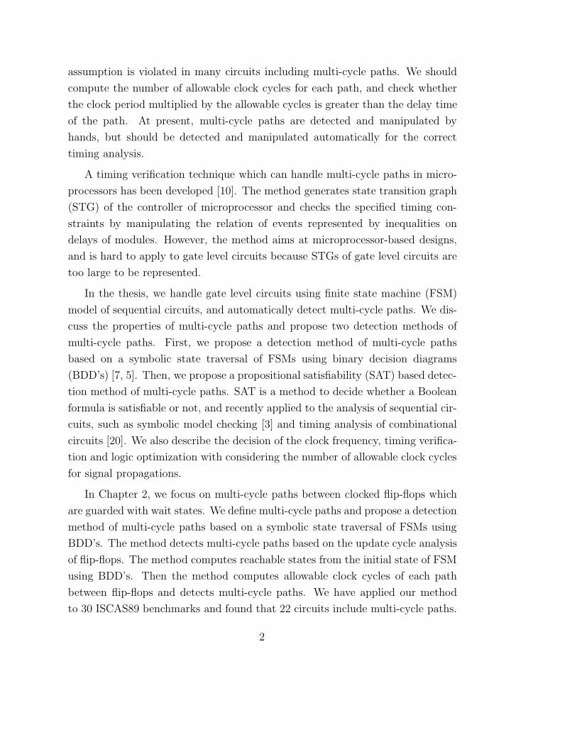
With the advances of VLSI technologies, the timing analysis and optimization of
sequential circuits become more and more important. The clock frequencies of
sequential circuits will become more than 2 GHz near the future. To cope with
timing issue in designing high-speed sequential circuits, the advance of timing
analysis system is demanded.
The clock frequencies of sequential circuits are decided based on the maximum
delay time of paths between clocked flip-flops in the circuit. Hence, the precise
estimation of the maximum delay time is important in deciding the proper clock
frequency. The maximum delay can be computed as the longest path of the
weighted graph corresponding to the circuit, where nodes in the graph are logic
gates in the circuit and the weight of the node is the delay time of each gate [14].
In some case, such topological maximum delay paths cannot be sensitized
with any input patterns and therefore become false paths. Many works have
been done to detect false paths and to maximize the clock frequency [2, 6, 1].
On the other hand, in circuits, there exist paths which are sensitizable but do
not affect the clock frequency. These paths are multi-cycle paths between clocked
flip-flops. Multi-cycle paths are the paths whose input is stable for several clock
cycles before the output is required, and 2 or more clock cycles are allowed for
signal propagations. Hence, the delay time of multi-cycle paths can be greater
than the clock period.
The clock frequencies of sequential circuits are generally decided under the
assumption that all paths propagate signals within one clock cycle. However, the
1
assumption is violated in many circuits including multi-cycle paths. We should
compute the number of allowable clock cycles for each path, and check whether
the clock period multiplied by the allowable cycles is greater than the delay time
of the path. At present, multi-cycle paths are detected and manipulated by
hands, but should be detected and manipulated automatically for the correct
timing analysis.
A timing verification technique which can handle multi-cycle paths in micro-
processors has been developed [10]. The method generates state transition graph
(STG) of the controller of microprocessor and checks the specified timing con-
straints by manipulating the relation of events represented by inequalities on
delays of modules. However, the method aims at microprocessor-based designs,
and is hard to apply to gate level circuits because STGs of gate level circuits are
too large to be represented.
In the thesis, we handle gate level circuits using finite state machine (FSM)
model of sequential circuits, and automatically detect multi-cycle paths. We dis-
cuss the properties of multi-cycle paths and propose two detection methods of
multi-cycle paths. First, we propose a detection method of multi-cycle paths
based on a symbolic state traversal of FSMs using binary decision diagrams
(BDD’s) [7, 5]. Then, we propose a propositional satisfiability (SAT) based detec-
tion method of multi-cycle paths. SAT is a method to decide whether a Boolean
formula is satisfiable or not, and recently applied to the analysis of sequential cir-
cuits, such as symbolic model checking [3] and timing analysis of combinational
circuits [20]. We also describe the decision of the clock frequency, timing verifica-
tion and logic optimization with considering the number of allowable clock cycles
for signal propagations.
In Chapter 2, we focus on multi-cycle paths between clocked flip-flops which
are guarded with wait states. We define multi-cycle paths and propose a detection
method of multi-cycle paths based on a symbolic state traversal of FSMs using
BDD’s. The method detects multi-cycle paths based on the update cycle analysis
of flip-flops. The method computes reachable states from the initial state of FSM
using BDD’s. Then the method computes allowable clock cycles of each path
between flip-flops and detects multi-cycle paths. We have applied our method
to 30 ISCAS89 benchmarks and found that 22 circuits include multi-cycle paths.
2
11 circuits among them include multi-cycle paths which are critical paths, where
the delay is measured as the number of gates on the path. Experimental results
show that many multi-cycle paths exist in sequential circuits.
In Chapter 3, we propose a SAT based detection method of multi-cycle paths.
The method generates a conjunctive normal form (CNF) formula which is satisfi-
able if and only if the path is not a multi-cycle path, and checks the satisfiability
of the formula with a SAT prover. In the conversion from multi-level circuits
into CNF formulae, the size of resulting CNF formulae may grow exponentially.
To reduce the size of CNF formulae, we introduce heuristics on the conversion.
The set of reachable states is hard to manipulate with SAT based-methods, so we
adopt an approximation that all states are reachable from the initial state. By
this approximation, some multi-cycle paths may not be detected, but there are
many detectable multi-cycle paths in large circuits. We have applied our method
to ISCAS89 benchmarks and other sample circuits. Experimental results show
the improvement in the size of manipulatable circuits, especially hard circuits for
BDD manipulation, and show 54 % of multi-cycle paths can be detected using
the SAT-based method under the assumption that all states are reachable.
In Chapter 4, we describe logic optimization with the information of detected
multi-cycle paths. In logic optimization, the area of circuits is reduced by chang-
ing multi-cycle path parts to small circuits with long path delay, and by replacing
gates on the path with small and slow gates.
3

Chapter 2
Multi-Cycle Path Analysis Based
on Symbolic State Traversal of
FSM
2.1. Introduction
The clock frequency of a sequential logic circuit is decided based on the maxi-
mum delay of the combinational parts of the circuit. The precise estimation of
the maximum delay is important in deciding the proper clock frequency. The
maximum delay can be computed as the longest path of the weighted graph cor-
responding to the circuit, where nodes in the graph are logic gates in the circuit
and the weight of the node is the delay time of each gate. The computational
complexity of the maximum delay computation is proportional to the size of the
graph.
In some case, such topological maximum delay paths cannot be sensitized
with any input patterns and therefore become false paths. Many researches have
been done to detect false paths and to minimize the clock period for obtaining the
maximum clock frequency [2, 6, 1]. False paths are classified into combinational
false paths and sequential false paths. Combinational false paths are the paths
where we have no input patterns to sensitize these paths. Sequential false paths
are the paths which can be sensitized only by unreachable states of the circuit.
Note that these combinational and sequential false paths are non-sensitizable
5
paths.
In logic circuits, there may exist paths which are sensitizable but do not affect
the clock period. Within such paths, we focus on multi-cycle paths where 2 or
more clock cycles are allowed for signal propagations. We describes properties of
multi-cycle paths and propose a detection method based on Finite State Machine
(FSM) model of logic circuits.
The rest of this chapter is organized as follows. In Section 2.2, we show
preliminaries. Section 2.3 shows an example of a multi-cycle path and Section
2.4 describes the update cycle analysis of flip-flops. In Section 2.5, we show the
detection method of multi-cycle paths. Experimental results are shown in Section
2.6.
2.2. Finite State Machines
Here, we show a definition of a finite state machine (FSM) based on [11] for the
analysis of multi-cycle paths.
Definition 2.1 An FSM M is a 6-tuple (S, Σ, Γ, δ, λ, q0) where
• S is a finite set of states,
• Σ is an input alphabet,
• Γ is an output alphabet,
• δ : S × Σ → S is a state transition function,
• λ : S × Σ → Γ is an output function,
• q0(∈ S) is the initial state.
✷
The behavior of M = (S, Σ, Γ, δ, λ, q0) with respect to an input sequence
a1a2 . . . . . . an (ai ∈ Σ) is a sequence of states q0q1 . . . qn (qi ∈ S) and a sequence
of outputs o1o2 . . . on (oi ∈ Γ) satisfying qi = δ(qi−1, ai) and oi = λ(qi−1, ai).
Let Σ∗ be a set of all input sequences over Σ, and let Σk be a set of input
sequences with length k. We use ε as the sequence of length 0.
To represent the behavior of M , the domain of δ and λ are extended, and
δ∗ : S × Σ∗ → S and λ∗ : S × Σ∗ → Γ∗ are introduced.
6
Definition 2.2 δ∗ : S × Σ∗ → S is defined as follows:• δ∗(q, ε) = q
• δ∗(q, xa) = δ(δ∗(q, x), a), (a ∈ Σ, x ∈ Σ∗)✷
Definition 2.3 λ∗ : S × Σ∗ → Γ∗ is defined as follows:• λ∗(q, ε) = ε
• λ∗(q, xa) = λ∗(q, x) · λ(δ∗(q, x), a), (a ∈ Σ, x ∈ Σ∗)✷
Note that real sequential logic circuits consist of flip-flops and combinational
parts, and the flip-flops are modeled as a state in the FSM model. In other
words, a state of the FSM model corresponds to the tuple of these values of all
flip-flops at each time, and λ corresponds to a tuple of values of primary outputs
of sequential circuits. In the following, we focus on the values of specific flip-flops,
and use λr to denote the output function representing the value of a flip-flop r.
It should be also noted that we deal only with edge-triggered flip-flops, but not
with transparent latches.
[Example]
Consider a 4-bit synchronous up counter shown in Figure 2.1. The counter con-
sists of 4 flip-flops ff0, ff1, ff2 and ff3. The value of these flip-flops changes as (ff0,
ff1, ff2, ff3) = (0, 0, 0, 0), (1, 0, 0, 0), (0, 1, 0, 0), ... synchronized with the
clock signal when in is 1.
FSM of the counter is shown in Figure 2.2, where S = {q0, q1, q2, q3, q4, q5,
q6, q7, q8, q9, q10, q11, q12, q13, q14, q15}, and the initial state is q0. Labels
of transitions represent the value of the input of the circuit in and the tuple of
values of all flip-flops. For instance, 1/1000 represents that the value of the input
is 1 and the tuple of values of flip-flops is (ff0, ff1, ff2, ff3) = (1, 0, 0, 0).
In the following, the 4-bit counter shown in Figure 2.1 and its FSM shown in
Figure 2.2 are used to illustrate our multi-cycle paths detection method.
7
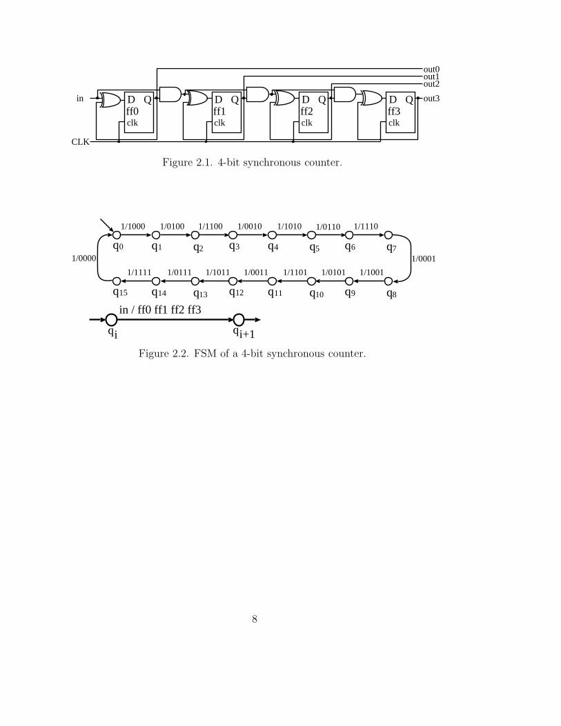
in out3
out2out1out0
CLK
D Qff3clk
D Qff2clk
D Qff1clk
D Qff0clk
Figure 2.1. 4-bit synchronous counter.
q0 q2q1 q3 q5q4 q7q6
q15 q13q14 q12 q10q11 q8q9
1/0001
1/0010
1/0011
1/0100
1/0101
1/0110
1/0111
1/1000
1/1001
1/1010
1/1011
1/1100
1/1101
1/1110
1/1111
1/0000
in / ff0 ff1 ff2 ff3
qi qi+1
Figure 2.2. FSM of a 4-bit synchronous counter.
8
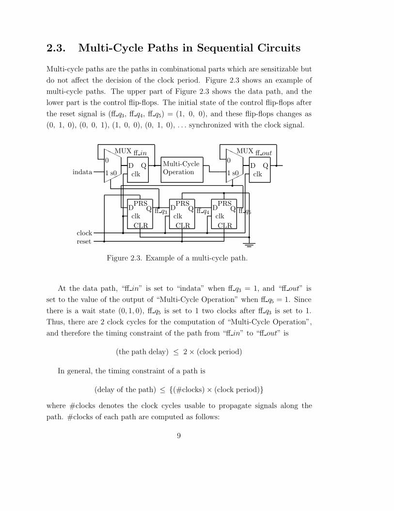
2.3. Multi-Cycle Paths in Sequential Circuits
Multi-cycle paths are the paths in combinational parts which are sensitizable but
do not affect the decision of the clock period. Figure 2.3 shows an example of
multi-cycle paths. The upper part of Figure 2.3 shows the data path, and the
lower part is the control flip-flops. The initial state of the control flip-flops after
the reset signal is (ff q3, ff q4, ff q5) = (1, 0, 0), and these flip-flops changes as
(0, 1, 0), (0, 0, 1), (1, 0, 0), (0, 1, 0), . . . synchronized with the clock signal.
✟✟✟
❍❍❍ MUX0
1 s0Dclk
Q Multi-CycleOperation
✟✟✟
❍❍❍ MUX0
1 s0Dclk
Q
Dclk
QPRS
CLR
Dclk
QPRS
CLR
Dclk
QPRS
CLR
� �
clock ��
�
��
�
�
reset ��
�
indata
�
ff q3 ff q4 ff q5
ff in ff out
Figure 2.3. Example of a multi-cycle path.
At the data path, “ff in” is set to “indata” when ff q3 = 1, and “ff out” is
set to the value of the output of “Multi-Cycle Operation” when ff q5 = 1. Since
there is a wait state (0, 1, 0), ff q5 is set to 1 two clocks after ff q3 is set to 1.
Thus, there are 2 clock cycles for the computation of “Multi-Cycle Operation”,
and therefore the timing constraint of the path from “ff in” to “ff out” is
(the path delay) ≤ 2× (clock period)
In general, the timing constraint of a path is
(delay of the path) ≤ {(#clocks)× (clock period)}where #clocks denotes the clock cycles usable to propagate signals along the
path. #clocks of each path are computed as follows:
9
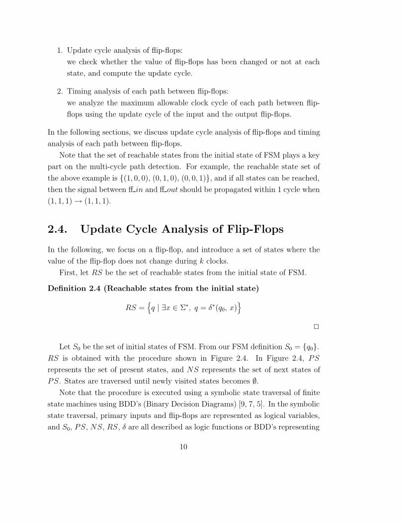
1. Update cycle analysis of flip-flops:
we check whether the value of flip-flops has been changed or not at each
state, and compute the update cycle.
2. Timing analysis of each path between flip-flops:
we analyze the maximum allowable clock cycle of each path between flip-
flops using the update cycle of the input and the output flip-flops.
In the following sections, we discuss update cycle analysis of flip-flops and timing
analysis of each path between flip-flops.
Note that the set of reachable states from the initial state of FSM plays a key
part on the multi-cycle path detection. For example, the reachable state set of
the above example is {(1, 0, 0), (0, 1, 0), (0, 0, 1)}, and if all states can be reached,
then the signal between ff in and ff out should be propagated within 1 cycle when
(1, 1, 1)→ (1, 1, 1).
2.4. Update Cycle Analysis of Flip-Flops
In the following, we focus on a flip-flop, and introduce a set of states where the
value of the flip-flop does not change during k clocks.
First, let RS be the set of reachable states from the initial state of FSM.
Definition 2.4 (Reachable states from the initial state)
RS ={q | ∃x ∈ Σ∗, q = δ∗(q0, x)
}
✷
Let S0 be the set of initial states of FSM. From our FSM definition S0 = {q0}.RS is obtained with the procedure shown in Figure 2.4. In Figure 2.4, PS
represents the set of present states, and NS represents the set of next states of
PS. States are traversed until newly visited states becomes ∅.Note that the procedure is executed using a symbolic state traversal of finite
state machines using BDD’s (Binary Decision Diagrams) [9, 7, 5]. In the symbolic
state traversal, primary inputs and flip-flops are represented as logical variables,
and S0, PS, NS, RS, δ are all described as logic functions or BDD’s representing
10
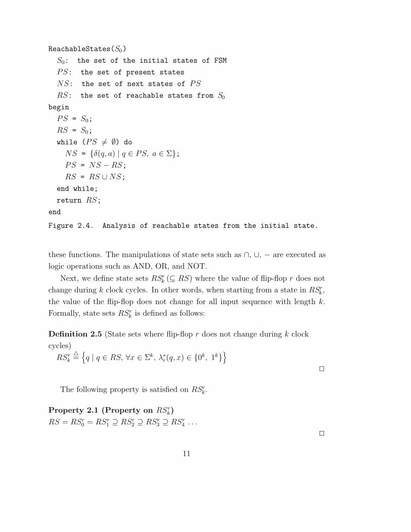
ReachableStates(S0)
S0: the set of the initial states of FSM
PS: the set of present states
NS: the set of next states of PS
RS: the set of reachable states from S0
begin
PS = S0;
RS = S0;
while (PS = ∅) do
NS = {δ(q, a) | q ∈ PS, a ∈ Σ};PS = NS −RS;
RS = RS ∪NS;
end while;
return RS;
end
Figure 2.4. Analysis of reachable states from the initial state.
these functions. The manipulations of state sets such as ∩, ∪, − are executed as
logic operations such as AND, OR, and NOT.
Next, we define state sets RSrk (⊆ RS) where the value of flip-flop r does not
change during k clock cycles. In other words, when starting from a state in RSrk,
the value of the flip-flop does not change for all input sequence with length k.
Formally, state sets RSrk is defined as follows:
Definition 2.5 (State sets where flip-flop r does not change during k clock
cycles)
RSrk
�=
{q | q ∈ RS, ∀x ∈ Σk, λ∗
r(q, x) ∈ {0k, 1k}}
✷
The following property is satisfied on RSrk.
Property 2.1 (Property on RSrk)
RS = RSr0 = RSr
1 ⊇ RSr2 ⊇ RSr
3 ⊇ RSr4 . . .
✷
11
Note that, if there is a strongly connected component where the value of r is the
same in any state, then RSrk = RSr
k+1 with some k. Let Kr be the maximum
number of k such that RSrk−1 = RSr
k.
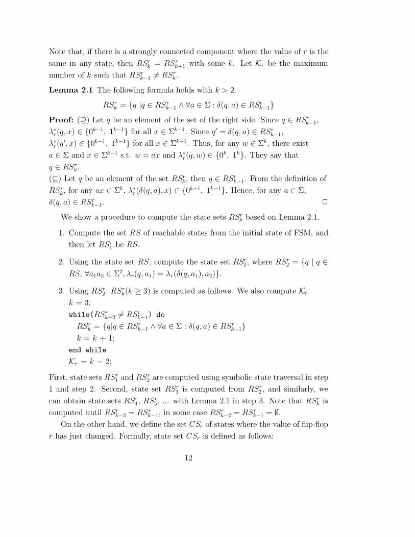
Lemma 2.1 The following formula holds with k > 2.
RSrk = {q |q ∈ RSr
k−1 ∧ ∀a ∈ Σ : δ(q, a) ∈ RSrk−1}
Proof: (⊇) Let q be an element of the set of the right side. Since q ∈ RSrk−1,
λ∗r(q, x) ∈ {0k−1, 1k−1} for all x ∈ Σk−1. Since q′ = δ(q, a) ∈ RSr
k−1,
λ∗r(q
′, x) ∈ {0k−1, 1k−1} for all x ∈ Σk−1. Thus, for any w ∈ Σk, there exist
a ∈ Σ and x ∈ Σk−1 s.t. w = ax and λ∗r(q, w) ∈ {0k, 1k}. They say that
q ∈ RSrk.
(⊆) Let q be an element of the set RSrk, then q ∈ RSr
k−1. From the definition of
RSrk, for any ax ∈ Σk, λ∗
r(δ(q, a), x) ∈ {0k−1, 1k−1}. Hence, for any a ∈ Σ,
δ(q, a) ∈ RSrk−1. ✷
We show a procedure to compute the state sets RSrk based on Lemma 2.1.
1. Compute the set RS of reachable states from the initial state of FSM, and
then let RSr1 be RS.
2. Using the state set RS, compute the state set RSr2 , where RSr
2 = {q | q ∈RS, ∀a1a2 ∈ Σ2, λr(q, a1) = λr(δ(q, a1), a2)}.
3. Using RSr2 , RSr
k(k ≥ 3) is computed as follows. We also compute Kr.
k = 3;
while(RSrk−2 = RSr
k−1) do
RSrk = {q|q ∈ RSr
k−1 ∧ ∀a ∈ Σ : δ(q, a) ∈ RSrk−1}
k = k + 1;
end while
Kr = k − 2;
First, state sets RSr1 and RSr
2 are computed using symbolic state traversal in step
1 and step 2. Second, state set RSr3 is computed from RSr
2 , and similarly, we
can obtain state sets RSr4 , RSr
5 , ... with Lemma 2.1 in step 3. Note that RSrk is
computed until RSrk−2 = RSr
k−1, in some case RSrk−2 = RSr
k−1 = ∅.On the other hand, we define the set CSr of states where the value of flip-flop
r has just changed. Formally, state set CSr is defined as follows:
12
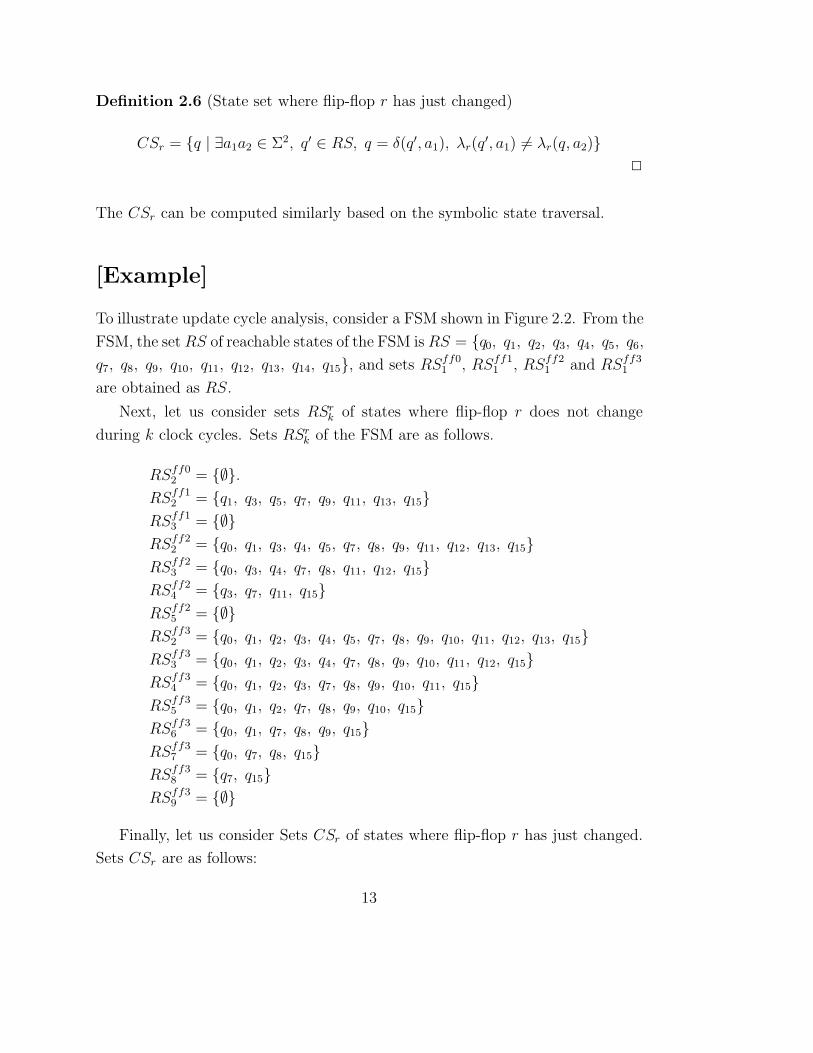
Definition 2.6 (State set where flip-flop r has just changed)
CSr = {q | ∃a1a2 ∈ Σ2, q′ ∈ RS, q = δ(q′, a1), λr(q′, a1) = λr(q, a2)}
✷
The CSr can be computed similarly based on the symbolic state traversal.
[Example]
To illustrate update cycle analysis, consider a FSM shown in Figure 2.2. From the
FSM, the set RS of reachable states of the FSM is RS = {q0, q1, q2, q3, q4, q5, q6,
q7, q8, q9, q10, q11, q12, q13, q14, q15}, and sets RSff01 , RSff1
1 , RSff21 and RSff3
1
are obtained as RS.
Next, let us consider sets RSrk of states where flip-flop r does not change
during k clock cycles. Sets RSrk of the FSM are as follows.
RSff02 = {∅}.
RSff12 = {q1, q3, q5, q7, q9, q11, q13, q15}
RSff13 = {∅}
RSff22 = {q0, q1, q3, q4, q5, q7, q8, q9, q11, q12, q13, q15}
RSff23 = {q0, q3, q4, q7, q8, q11, q12, q15}
RSff24 = {q3, q7, q11, q15}
RSff25 = {∅}
RSff32 = {q0, q1, q2, q3, q4, q5, q7, q8, q9, q10, q11, q12, q13, q15}
RSff33 = {q0, q1, q2, q3, q4, q7, q8, q9, q10, q11, q12, q15}
RSff34 = {q0, q1, q2, q3, q7, q8, q9, q10, q11, q15}
RSff35 = {q0, q1, q2, q7, q8, q9, q10, q15}
RSff36 = {q0, q1, q7, q8, q9, q15}
RSff37 = {q0, q7, q8, q15}
RSff38 = {q7, q15}
RSff39 = {∅}
Finally, let us consider Sets CSr of states where flip-flop r has just changed.
Sets CSr are as follows:
13
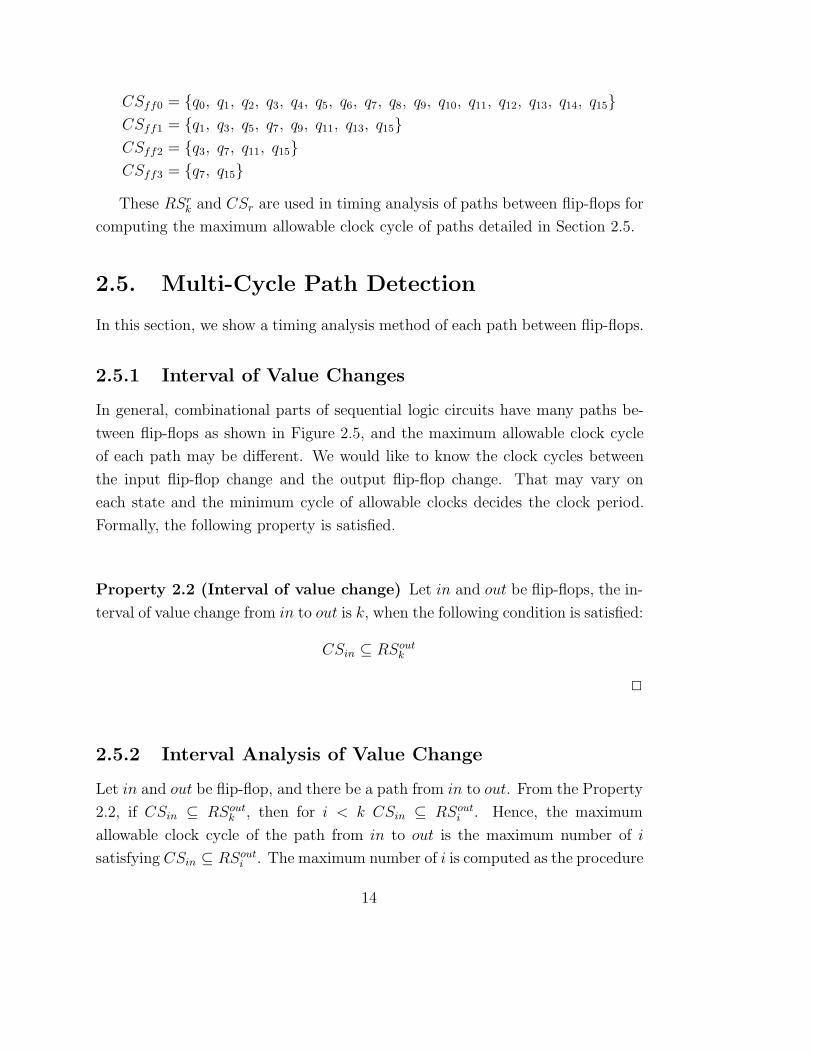
CSff0 = {q0, q1, q2, q3, q4, q5, q6, q7, q8, q9, q10, q11, q12, q13, q14, q15}CSff1 = {q1, q3, q5, q7, q9, q11, q13, q15}CSff2 = {q3, q7, q11, q15}CSff3 = {q7, q15}These RSr
k and CSr are used in timing analysis of paths between flip-flops for
computing the maximum allowable clock cycle of paths detailed in Section 2.5.
2.5. Multi-Cycle Path Detection
In this section, we show a timing analysis method of each path between flip-flops.
2.5.1 Interval of Value Changes
In general, combinational parts of sequential logic circuits have many paths be-
tween flip-flops as shown in Figure 2.5, and the maximum allowable clock cycle
of each path may be different. We would like to know the clock cycles between
the input flip-flop change and the output flip-flop change. That may vary on
each state and the minimum cycle of allowable clocks decides the clock period.
Formally, the following property is satisfied.
Property 2.2 (Interval of value change) Let in and out be flip-flops, the in-
terval of value change from in to out is k, when the following condition is satisfied:
CSin ⊆ RSoutk
✷
2.5.2 Interval Analysis of Value Change
Let in and out be flip-flop, and there be a path from in to out. From the Property
2.2, if CSin ⊆ RSoutk , then for i < k CSin ⊆ RSout
i . Hence, the maximum
allowable clock cycle of the path from in to out is the maximum number of i
satisfying CSin ⊆ RSouti . The maximum number of i is computed as the procedure
14
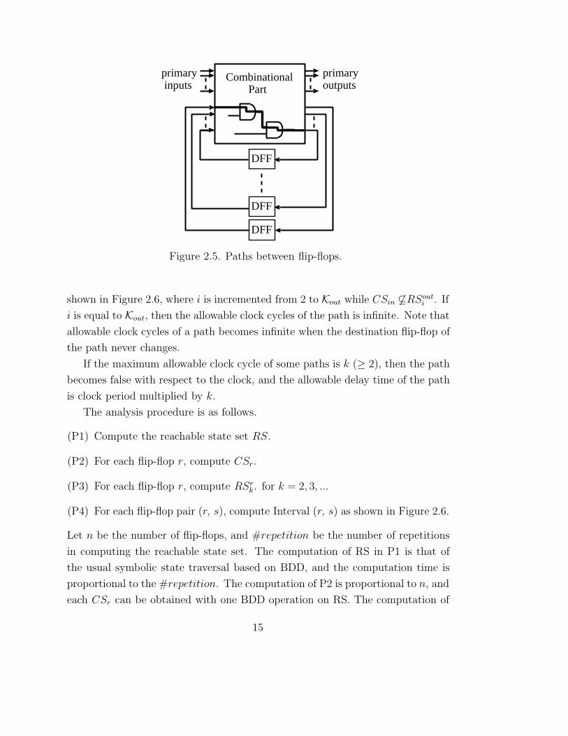
primaryoutputs
Combinational Part
primary inputs
DFF
DFF
DFF
Figure 2.5. Paths between flip-flops.
shown in Figure 2.6, where i is incremented from 2 to Kout while CSin ⊆RSouti . If
i is equal to Kout, then the allowable clock cycles of the path is infinite. Note that
allowable clock cycles of a path becomes infinite when the destination flip-flop of
the path never changes.
If the maximum allowable clock cycle of some paths is k (≥ 2), then the path
becomes false with respect to the clock, and the allowable delay time of the path
is clock period multiplied by k.
The analysis procedure is as follows.
(P1) Compute the reachable state set RS.
(P2) For each flip-flop r, compute CSr.
(P3) For each flip-flop r, compute RSrk. for k = 2, 3, ...
(P4) For each flip-flop pair (r, s), compute Interval (r, s) as shown in Figure 2.6.
Let n be the number of flip-flops, and #repetition be the number of repetitions
in computing the reachable state set. The computation of RS in P1 is that of
the usual symbolic state traversal based on BDD, and the computation time is
proportional to the #repetition. The computation of P2 is proportional to n, and
each CSr can be obtained with one BDD operation on RS. The computation of
15
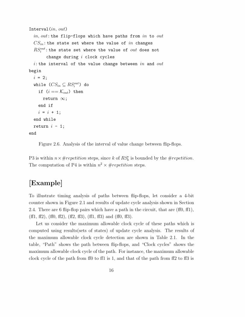
Interval(in, out)
in, out: the flip-flops which have paths from in to out
CSin: the state set where the value of in changes
RSouti : the state set where the value of out does not
change during i clock cycles
i: the interval of the value change between in and out
begin
i = 2;
while (CSin ⊆ RSouti ) do
if (i == Kout) then
return ∞;
end if
i = i + 1;
end while
return i - 1;
end
Figure 2.6. Analysis of the interval of value change between flip-flops.
P3 is within n×#repetition steps, since k of RSrk is bounded by the #repetition.
The computation of P4 is within n2 ×#repetition steps.
[Example]
To illustrate timing analysis of paths between flip-flops, let consider a 4-bit
counter shown in Figure 2.1 and results of update cycle analysis shown in Section
2.4. There are 6 flip-flop pairs which have a path in the circuit, that are (ff0, ff1),
(ff1, ff2), (ff0, ff2), (ff2, ff3), (ff1, ff3) and (ff0, ff3).
Let us consider the maximum allowable clock cycle of these paths which is
computed using results(sets of states) of update cycle analysis. The results of
the maximum allowable clock cycle detection are shown in Table 2.1. In the
table, “Path” shows the path between flip-flops, and “Clock cycles” shows the
maximum allowable clock cycle of the path. For instance, the maximum allowable
clock cycle of the path from ff0 to ff1 is 1, and that of the path from ff2 to ff3 is
16
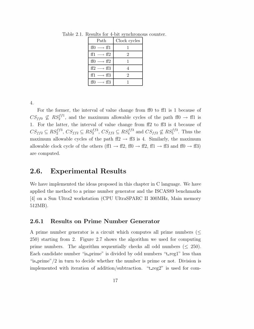
Table 2.1. Results for 4-bit synchronous counter.
Path Clock cycles
ff0 −→ ff1 1ff1 −→ ff2 2
ff0 −→ ff2 1
ff2 −→ ff3 4
ff1 −→ ff3 2
ff0 −→ ff3 1
4.
For the former, the interval of value change from ff0 to ff1 is 1 because of
CSff0 ⊆ RSff12 , and the maximum allowable cycles of the path ff0 → ff1 is
1. For the latter, the interval of value change from ff2 to ff3 is 4 because of
CSff2 ⊆ RSff32 , CSff2 ⊆ RSff3
3 , CSff2 ⊆ RSff34 and CSff2 ⊆ RSff3
5 . Thus the
maximum allowable cycles of the path ff2 → ff3 is 4. Similarly, the maximum
allowable clock cycle of the others (ff1 → ff2, ff0 → ff2, ff1 → ff3 and ff0 → ff3)
are computed.
2.6. Experimental Results
We have implemented the ideas proposed in this chapter in C language. We have
applied the method to a prime number generator and the ISCAS89 benchmarks
[4] on a Sun Ultra2 workstation (CPU UltraSPARC II 300MHz, Main memory
512MB).
2.6.1 Results on Prime Number Generator
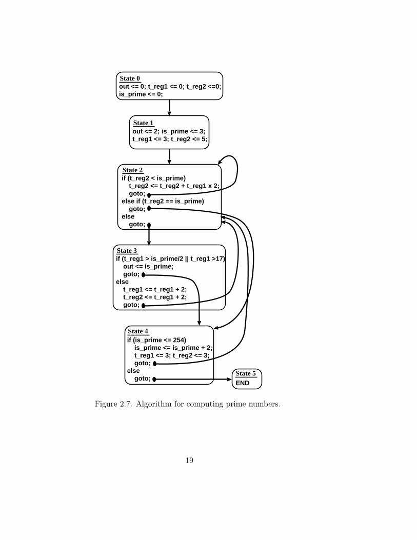
A prime number generator is a circuit which computes all prime numbers (≤250) starting from 2. Figure 2.7 shows the algorithm we used for computing
prime numbers. The algorithm sequentially checks all odd numbers (≤ 250).
Each candidate number “is prime” is divided by odd numbers “t reg1” less than
“is prime”/2 in turn to decide whether the number is prime or not. Division is
implemented with iteration of addition/subtraction. “t reg2” is used for com-
17
puting division. We have designed the prime number generator in VHDL. The
VHDL design is non-pipeline and includes hardware loop structures. We obtained
a gate level circuit from the VHDL design with the Synopsys Design Compiler1,
where the circuit consists of 35 flip-flops and about 500 gates.
We have applied our method to the circuit and examined 772 flip-flop pairs
which have paths between them. We have found 476 flip-flop pairs with allowable
clock cycles greater than 1. 190 pairs among them can be guessed from the state
transitions in the VHDL design. The others (286 pairs) are hard to guess from
VHDL description. 133 pairs of the 190 pairs relate to counters controlling the
hardware loop. The others of 190 pairs come from the structure of the circuit,
in which the value changes are controlled by wait states as shown in the Section
3. The number of repetitions in computing reachable states of the circuit was
11959. The elapsed CPU time was 3619.0 seconds on the Sun Ultra2.
We have checked critical paths in the prime number circuit, where the delay
is measured as the number of gates on the path. We have found 16 critical paths
(43 gates), and 14 of them have been detected by our method as paths whose
allowable clock cycles are more than 2.
These results show that many multi-cycle paths exist in sequential logic cir-
cuits.
1The Synopsys Design Compiler is licensed in the education program of VLSI Design andEducation Center (VDEC), the University of Tokyo. I would like to thank to VDEC (VLSIDesign and Education Center) for the support of Synopsys tools.
18
if (t_reg2 < is_prime) t_reg2 <= t_reg2 + t_reg1 x 2; goto;else if (t_reg2 == is_prime) goto;else goto;
if (is_prime <= 254) is_prime <= is_prime + 2; t_reg1 <= 3; t_reg2 <= 3; goto;else goto;
if (t_reg1 > is_prime/2 || t_reg1 >17) out <= is_prime; goto;else t_reg1 <= t_reg1 + 2; t_reg2 <= t_reg1 + 2; goto;
out <= 2; is_prime <= 3;t_reg1 <= 3; t_reg2 <= 5;
out <= 0; t_reg1 <= 0; t_reg2 <=0;is_prime <= 0;
END
State 0
State 1
State 2
State 3
State 4
State 5
Figure 2.7. Algorithm for computing prime numbers.
19
2.6.2 Results on ISCAS89 Benchmarks
We have applied our detection method to 32 ISCAS89 benchmarks [4] and found
multi-cycle flip-flop pairs with allowable clock cycles greater than 1 on 22 circuits.
Table 2.2 shows the statistics. In the table, “#In”,“#FF” and “#FF-pair” are
the number of primary inputs, flip-flops and connected pairs of flip-flops in the
circuit respectively. “#Rep” is the number of repetitions in computing reachable
states of the circuit. “#M-pair” is the number of flip-flop pairs whose maximum
allowable clock cycles are 2 or more.
The prime number generator and s838 include almost the same number of
flip-flops, but the elapsed CPU time of s838 was quite short compared with the
prime number generator. This is because #Rep of the prime number generator is
11959 and that of s838 is 17. Each repetition includes BDD manipulations, and
the execution time heavily depends on the #Rep.
We have checked critical paths in 30 benchmarks. The critical paths whose
allowable clock cycles are 2 or more have been found in 11 circuits. In Table 2.2,
† denotes that the circuit includes such critical paths.
20
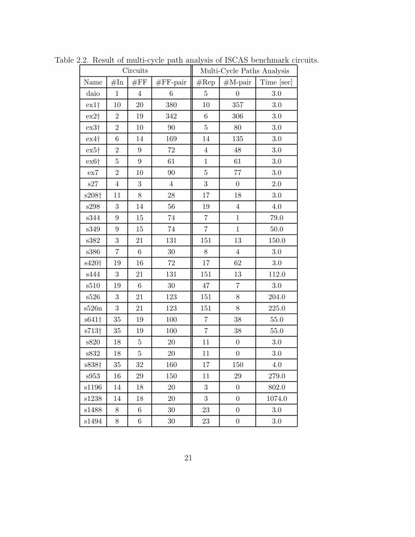
Table 2.2. Result of multi-cycle path analysis of ISCAS benchmark circuits.
Circuits Multi-Cycle Paths Analysis
Name #In #FF #FF-pair #Rep #M-pair Time [sec]
daio 1 4 6 5 0 3.0
ex1† 10 20 380 10 357 3.0
ex2† 2 19 342 6 306 3.0
ex3† 2 10 90 5 80 3.0
ex4† 6 14 169 14 135 3.0ex5† 2 9 72 4 48 3.0
ex6† 5 9 61 1 61 3.0
ex7 2 10 90 5 77 3.0
s27 4 3 4 3 0 2.0
s208† 11 8 28 17 18 3.0s298 3 14 56 19 4 4.0
s344 9 15 74 7 1 79.0
s349 9 15 74 7 1 50.0
s382 3 21 131 151 13 150.0
s386 7 6 30 8 4 3.0s420† 19 16 72 17 62 3.0
s444 3 21 131 151 13 112.0
s510 19 6 30 47 7 3.0
s526 3 21 123 151 8 204.0
s526n 3 21 123 151 8 225.0
s641† 35 19 100 7 38 55.0s713† 35 19 100 7 38 55.0
s820 18 5 20 11 0 3.0
s832 18 5 20 11 0 3.0
s838† 35 32 160 17 150 4.0
s953 16 29 150 11 29 279.0s1196 14 18 20 3 0 802.0
s1238 14 18 20 3 0 1074.0
s1488 8 6 30 23 0 3.0
s1494 8 6 30 23 0 3.0
21
2.7. Conclusion
In this chapter, we have proposed a method to detect the multi-cycle paths.
Multi-cycle paths exist when input and output flip-flops of the paths are guarded
with wait states, and the delay time of the path can be greater than the clock
period. More precisely, we should decide the clock period under the constraint
where the delay of the path is smaller than the clock period multiplied by the
maximum allowable clock cycle.
In the detection of multi-cycle paths, we use the symbolic state traversal to
obtain the state sets with update cycle more than 2. We have applied the detec-
tion method to ISCAS benchmarks and found multi-cycle paths on 22 circuits in
30 finite state machine benchmarks. Since our method includes BDD manipula-
tions, the applicable circuit size is restricted by the memory size for manipulating
BDD’s. At present technology, circuits including 50-100 flip-flops can be manip-
ulated. For applying large circuits, we should consider (1) circuit partitioning:
a method to partition a large circuit to independent small modules for which
our method can be applied, (2) analysis on VHDL sources: a method to detect
multi-cycle paths on VHDL source and to omit the gate level analysis for such
paths, and (3) abstraction of datapath: a method to reduce datapath width of
some flip-flop pairs which can be analyzed on VHDL sources.
The method proposed in this chapter can be applied to decide the maximum
clock frequency of sequential logic circuits and to optimize the delay of some
operations in logic synthesis systems.
22
Chapter 3
Multi-Cycle Path Analysis Based
on Propositional Satisfiability
3.1. Introduction
Two multi-cycle path detection methods [10, 16] have been proposed. One is
based on the analysis of state transition graphs of the controllers of micropro-
cessors [10], and the other is based on the symbolic state traversal of finite state
machines (FSMs) [16]. Both methods are based on the state traversal of finite
state machines, and for large circuits these suffer from the huge size of reachable
states.
Propositional satisfiability (SAT) is a method to decide whether a Boolean for-
mula is satisfiable or not, and has been used in logic comparison and test pattern
generation [13]. Recently, SAT is applied to the analysis of sequential circuits,
such as symbolic model checking [3] and timing analysis of combinational circuits
[20]. SAT is also used to the critical delay path analysis [20] of combinational
logic circuits.
In this chapter, we present a SAT-based multi-cycle path detection method.
The method generates a conjunctive normal form (CNF) formula which is satisfi-
able if and only if the path is not a multi-cycle path, and checks the satisfiability
of the formula with a SAT prover. To reduce the size of CNF formulae, we also
introduce heuristics on the conversion from multi-level circuits into CNF formu-
lae. The heuristics adaptively insert intermediate variables with considering the
23
structure of logic networks in the conversion, and reduce the size of CNF formulae.
The set of reachable states is hard to manipulate based on SAT based-methods,
so we adopt an approximation that all states are reachable. By this approxima-
tion, some multi-cycle paths may not be detected, but there are many detectable
multi-cycle paths in large circuits under the approximation as shown in the chap-
ter. Note that such paths cannot be detected without the approximation, and
that the information of the detected paths is effective to estimate or optimize the
timing issues of the parts including the paths.
We have implemented our method and tested it on ISCAS89 benchmarks [4]
and other sample circuits. Experimental results show the improvement in the
size of manipulatable circuits, especially hard circuits for BDD manipulation.
This chapter is organized as follows. In the next section, we present Propo-
sitional Satisfiability. In Section 3.3, we define multi-cycle paths and show a
detection method of multi-cycle paths. In Section 3.4, we present a satisfiability
based multi-cycle path detection method. In Section 3.5, we present heuristics
on the conversion from multi-level circuits into CNF formulae. In Section 3.6, we
show the experimental results.
3.2. Propositional Satisfiability
Let xi be a propositional variable, and xi be the negation of xi. A variable and its
negation are called literals. The disjunction (OR, ∨) of literals such as x1∨x2 and
x1∨x2∨x3 is a clause. The conjunction of clauses such as (x1∨x2)∧(x1∨x2∨x3)
is a conjunctive normal form (CNF) formula. A CNF formula f over x1, ..., xl is
a CNF formula including only literals x1, x1, x2, x2, ..., xl, xl.
Let (x1, ..., xl) be a tuple of propositional variables and f be a CNF formula
over x1, ..., xl. We can assign T(true) or F(false) for xi. If xi is assigned T(F),
then xi is assigned F(T). A clause has value T, if T is assigned for one of literals
in the clause. A CNF formula has value T, if all clauses have value T. A CNF
formula f is satisfiable if f has value T with some value assignments for variables.
24
3.3. Multi-Cycle Path Detection Based on Sym-
bolic State Traversal of FSM
Given a circuit, multi-cycle paths are detected by analyzing FSM model of the
circuit as described in Chapter 2. At first, we compute the set RS of reachable
states from the initial state, and we analyze properties of FSM on RS.
Let rin and rout be flip-flops, and there be a path from rin to rout. If the value
of rout does not change at the next clock of the clock when the value of rin has
just changed, then the propagation of signals can use 2 or more clock cycles. Note
that the change of rin does not contribute to the value of rout. We obtain the
following condition specifying the multi-cycle property on a path from rin to rout:
∀q ∈ RS, ∀a, a′ ∈ Σ,[(q′ = δ(q, a)) ∧ (q′′ = δ(q′, a′)) (1)
→((q(rin) = q′(rin)) → (q′(rout) = q′′(rout))
)].
Formula (1) denotes that if the value of rin changes at the state transition from q
to q′, then the value of rout does not change at the state transition from q′ to q′′,
where q, q′ and q′′ are reachable from the initial state and q(r) denotes the value
of a flip-flop r under the state q. Similarly, the condition specifying the path can
use 3 or more clock cycles can be obtained by extending Formula (1).
In the following, we focus on Formula (1) specifying the allowable clock cycles
to be 2 or more. At present, the symbolic state traversal of the FSM is the
best way to compute RS, and a BDD-based multi-cycle path detection method
has been proposed [16]. However, the method is hard to apply to large circuits.
Hence, we relax the above condition a little and check the relaxed condition using
propositional satisfiability.
3.4. Multi-Cycle Path Detection Using Satisfia-
bility
In this section, we describe an algorithm that detects multi-cycle paths based on
propositional satisfiability.
25
C C
a a’Ca(t)
DFF
q(t+1)q(t)
q’ q’’q
(a) A sequential circuit (b) A time expansion
Figure 3.1. Time expansion of a sequential circuit.
SAT is not suitable for computing the reachable state set. Thus we abandon
the computation and assume that all states are reachable from the initial state.
The following formula is used in the multi-cycle path analysis instead of Formula
(1).
∀q ∈ S, ∀a, a′ ∈ Σ,[(q′ = δ(q, a)) ∧ (q′′ = δ(q′, a′)) (2)
→((q(rin) = q′(rin)) → (q′(rout) = q′′(rout))
)].
Since Formula (2) takes into account all states, there is a possibility that sev-
eral multi-cycle paths can not be detected by the analysis as we described in
2.3. However, we should adopt some approximation to manipulate large circuits.
Experimental results show the effect of the approximation. The accuracy of the
analysis is reduced. The information of detected multi-cycle paths, however, is
the same as that with the exact analysis, and is effective to estimate or optimize
the parts including the paths.
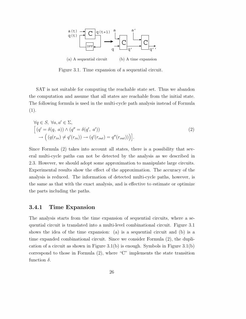
3.4.1 Time Expansion
The analysis starts from the time expansion of sequential circuits, where a se-
quential circuit is translated into a multi-level combinational circuit. Figure 3.1
shows the idea of the time expansion: (a) is a sequential circuit and (b) is a
time expanded combinational circuit. Since we consider Formula (2), the dupli-
cation of a circuit as shown in Figure 3.1(b) is enough. Symbols in Figure 3.1(b)
correspond to those in Formula (2), where “C” implements the state transition
function δ.
26
3.4.2 Propositional Formula for Multi-Cycle Path Analy-
sis
Based on Formula (2), we define a propositional formula F for detecting multi-
cycle paths.
Let rin and rout be the input and output flip-flops to be checked, and let
≡ and ≡ denote equivalence and negation of equivalence between propositional
variables respectively. The following propositional formula F becomes true if the
path from rin to rout can use 2 clock cycles:
F�= T (a, q, q′) ∧ T (a′, q′, q′′) (3)
→((q(rin) ≡ q′(rin)) → (q′(rout) ≡ q′′(rout))
),
where T (a, q, q′) = 1 iff q′ = δ(q, a) and T (a′, q′, q′′) = 1 iff q′′ = δ(q′, a′). Note
that T (a, q, q′) represents a logic formula which is implemented by a multi-
level circuit, where a, q and q′ are coded in binary and represented by a tuple
of propositional variables. Also note that q(rin) and q(rout) are propositional
variables corresponding to rin and rout in the tuple of the state variables for the
state q.
If F is unsatisfiable, then F is always true for any q, a and a′, and therefore
we can decide that the allowable clock cycle is 2 or more. We convert F into
CNF formulae, and check the unsatisfiability of F using a SAT prover. We can
obtain CNF of F using a conversion rule a ≡ b ⇒ (a ∨ b) ∧ (a ∨ b):
F = T (a, q, q′) ∧ T (a′, q′, q′′) (4)
∧(q(rin) ∨ q′(rin)) ∧ (q(rin) ∨ q′(rin))
∧(q′(rout) ∨ q′′(rout)) ∧ (q′(rout) ∨ q′′(rout)).
Note that T (a, q, q′) and T (a′, q′, q′′) are the same logic formula with different
variables. In the following we discuss a method to generate CNF of T (a, q, q′).
3.5. Conversion to CNF Formula
In this section we show a method to convert multi-level combinational circuits
into CNF formulae and heuristics on the conversion.
27
3.5.1 Conversion to CNF Formula without New Variables
In general, CNF formulae can be generated from multi-level combinational cir-
cuits using the following conversion rules: (f1 ≡ f2) ⇒ (f1 ∨ f2) ∧ (f1 ∨ f2),
(f1 ≡ f2) ⇒ (f1 ∨ f2) ∧ (f1 ∨ f2) and (f1 ∧ f2) ∨ f3 ⇒ (f1 ∨ f3) ∧ (f2 ∨ f3). The
size of resulting CNF formulae may grow exponentially, and we should introduce
heuristic techniques on the conversion. For example, let f1, f2, f3 and f4 be sub-
formulae which are not CNF, and we consider a formula (f1 ∧ f2)∨ (f3 ∧ f4). The
formula is converted into (f1 ∨ f3)∧ (f1 ∨ f4)∧ (f2 ∨ f3)∧ (f2 ∨ f4), and the size of
the formula can be twice. If f3 and f4 are f31∧f32 and f41∧f42 respectively, then
f1 and f2 should be duplicated in the conversion to CNF and the size of CNF can
be exponential with respect to the size of the original formula in the worst case.
As above, ∨ causes exponential growth of formulae in the conversion to CNF.
In addition to ∨, ≡ and ≡ cause exponential growth of formulae because both
≡ and ≡ are converted into two ∨ using the above rules. In the following, we
assume that multi-level combinational logic circuits consist of AND, OR, NOT
and XOR ( ≡) gates.
3.5.2 Conversion to CNF Formula with New Variables
To avoid the problem in the conversion to CNF, we apply a method which in-
serts new propositional variables in the conversion and reduces the size of CNF
formulae without affecting the satisfiability of formulae [18].
For example, let a0, a1, b0, b1 and c0 be propositional variables, and we consider
a formula a1 ≡ b1 ≡ ((a0∧b0)∨((a0 ≡ b0)∧c0)). If we insert new variables x1, x2,
x3, x4 and x5 for a1 ≡ b1, x3 ∨ x4, a0 ∧ b0, x5 ∧ c0 and a0 ≡ b0 respectively, then
we obtain an equivalent formula as follows: (x1 ≡ x2)∧ (x1 ≡ (a1 ≡ b1))∧ (x2 ≡(x3 ∨ x4)) ∧ (x3 ≡ (a0 ∧ b0)) ∧ (x4 ≡ (x5 ∧ c0)) ∧ (x5 ≡ (a0 ≡ b0)). From
the equivalent formula, we obtain the following CNF formula applying the above
rules: (x5∨a0∨b0)∧(x5∨a0∨b0)∧(x5∨b0∨a0)∧(x5∨a0∨b0)∧(x4∨x5∨c0)∧(x4∨c0)∧(x4∨x5)∧(x3∨a0∨b0)∧(x3∨a0)∧(x3∨b0)∧(x2∨x3∨x4)∧(x2∨x4)∧(x2∨x3)∧(x1∨a1∨b1)∧(x1∨a1∨b1)∧(x1∨b1∨a1)∧(x1∨a1∨b1)∧(x1∨x2)∧(x1∨x2), and
the number of literals of the formula is 49. New variables are useful for reducing
the size of CNF formulae and the number of literals.
28
On the other hand, if we do not insert new variables, we obtain the following
CNF formula applying the above conversion rules: (a0∨a1∨b0∨b1)∧ (a0∨a1∨b0∨b1)∧(a0∨a1∨b0∨b1∨c0)∧(a0∨a1∨b0∨b1∨c0)∧(a0∨a1∨b0∨b1∨c0)∧(a0∨a1∨b0∨b1∨c0)∧(a0∨a1∨b1∨c0)∧(a0∨a1∨b1∨c0)∧(a1∨b0∨b1∨c0)∧(a1∨b0∨b1∨c0)∧(a0∨a1∨b0∨b1)∧(a1∨a0∨b0∨b1)∧(a0∨a1∨b0∨b1)∧(a0∨a1∨b0∨b1),
and the number of literals of the formula is 60. If we introduce variables for any
logic operation with 2 operands, we can easily show that the size of CNF is less
than 12 × (the number of operations) as shown in [18].
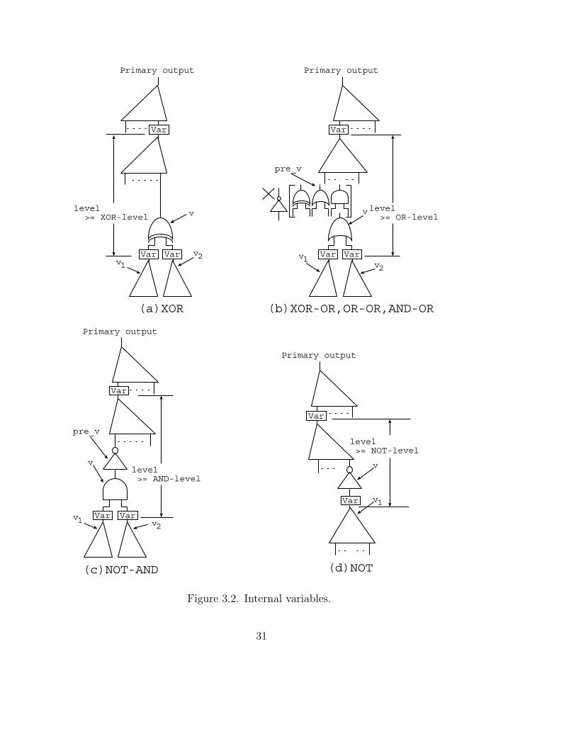
3.5.3 Adaptive Variable Insertion
In [18], new variables are inserted for all logic gates in the conversion. For many
circuits, the method is not best on the size of generated formulae. For example,
we consider a1 ≡ b1 ≡ ((a0 ∧ b0) ∨ ((a0 ≡ b0)) ∧ c0) again. If we insert only two
new variables x1 and x2 for a1 ≡ b1 and (a0 ∧ b0) ∨ ((a0 ≡ b0) ∧ c0), then we
obtain an equivalent formula as follows: (x1 ≡ x2) ∧ (x1 ≡ (a1 ≡ b1)) ∧ (x2 ≡((a0∧b0)∨((a0 ≡ b0)∧c0))). From the equivalent formula, we obtain the following
CNF formula applying the above conversion rules: (x2∨a0∨c0)∧(x2∨b0∨c0)∧(x2∨a0∨b0)∧(x2∨a0∨b0)∧(x2∨a0∨b0)∧(x2∨a0∨b0∨c0)∧(x2∨a0∨b0∨c0)∧(x1∨a1∨b1)∧(x1∨a1∨b1)∧(x1∨a1∨b1)∧(x1∨a1∨b1)∧(x1∨x2)∧(x1∨x2), and
the number of literals of the formula is 39. The size of CNF formulae is reduced
by selective variable insertion. We should control the number of new variables
and reduce the size of CNF formulae because the execution time of SAT provers
is affected by the size of formulae.
In the variable insertion, we should treat carefully XOR and OR gates because
XOR and OR gates cause exponential growth of CNF formulae as we described
in Section 3.5.1. For AND and NOT gates, we need not introduce variables, since
they are suitable to convert CNF formulae. Hence, we use threshold values for
controlling the variable insertion, that are sensitive to the logic type of a gate
and the depth of logic gates. Our method adaptively inserts new variables based
on the structure of logic networks, namely, the depth of logic gates from primary
output and that from newly inserted variables are considered. Figure 3.2 shows
the idea. We classify 4 cases as shown in the figure, and introduce 4 parameters
on the level. In Figure 3.2, “v” denotes a logic gate which we focus on, “Var”-s
29
denote new variables which we inserted. “XOR-level”, “OR-level”, “AND-level”
and “NOT-level” are thresholds that denote the maximum depth from newly
inserted variables. We insert new variables at the focusing gate “v” when the
number of levels of “v” from the nearest variables exceeds the thresholds. The
circuit is divided into sub-circuits with almost the same level. For example, the
OR gate in Figure 3.2(b) is considered. If the level of the OR gate from the
nearest variable is over “OR-level” and “pre v” is not a NOT gate, then we
introduce new variables for fan-ins of the OR gate. Note that we do not insert a
new variable if “pre v” is a NOT gate because NOT-OR corresponds to an AND
gate in the conversion to CNF. Similarly, we insert a new variable for NOT-AND
as in Figure 3.2(c) because NOT-AND corresponds to an OR gate that causes the
exponential growth of formulae. We show the effect of this method on reducing
CNF size in Section 6.
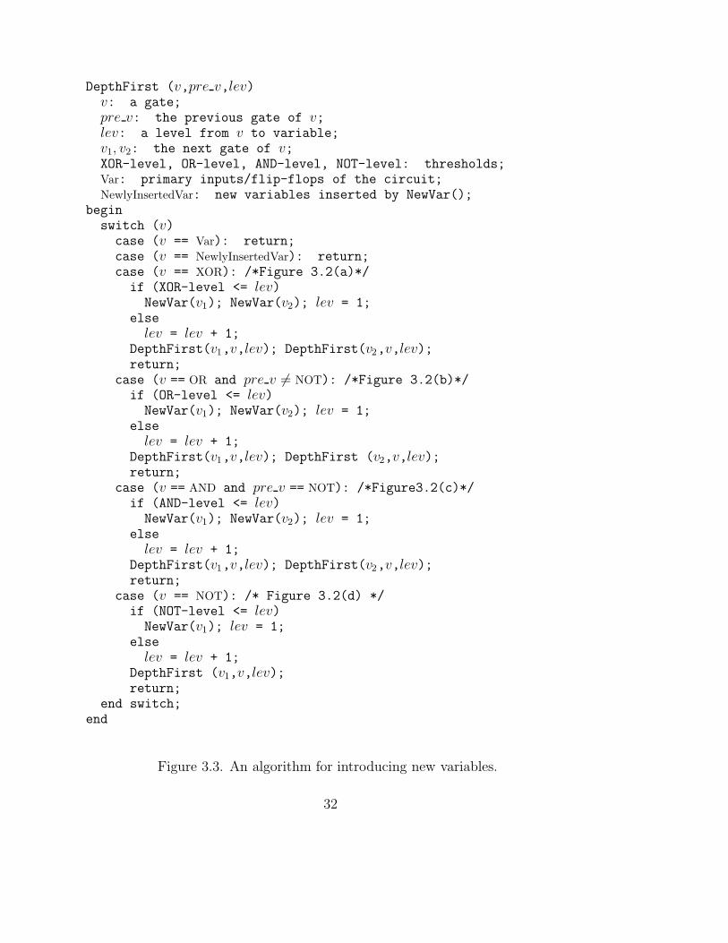
Figure 3.3 shows an algorithm for inserting new variables. The analysis starts
from the primary outputs of multi-level logic circuits, and goes backward toward
primary inputs based on the depth first search algorithm. At first, lev is set to
1, and then lev is incremented for every recursive calls of DepthFirst(). If the
value of lev exceeds the threshold depending the type of each gate, then new
variables are inserted for fan-ins by NewVar().
30
level >= NOT-level
(d)NOT
Var
Var
v
v1
Primary output
(c)NOT-AND
level >= AND-level
Var Var
Var
1v
pre_v
v
2v
Primary output
(b)XOR-OR,OR-OR,AND-OR
level >= OR-level
VarVar
Var
2v
pre_v
1v
Primary output
v
Primary output
2
(a)XOR
Var Var
Var
v
v
1v
level >= XOR-level
Figure 3.2. Internal variables.
31
DepthFirst (v,pre v,lev)v: a gate;pre v: the previous gate of v;lev: a level from v to variable;v1, v2: the next gate of v;XOR-level, OR-level, AND-level, NOT-level: thresholds;Var: primary inputs/flip-flops of the circuit;NewlyInsertedVar: new variables inserted by NewVar();
beginswitch (v)case (v == Var): return;case (v == NewlyInsertedVar): return;case (v == XOR): /*Figure 3.2(a)*/
if (XOR-level <= lev)NewVar(v1); NewVar(v2); lev = 1;
elselev = lev + 1;
DepthFirst(v1,v,lev); DepthFirst(v2,v,lev);return;
case (v == OR and pre v = NOT): /*Figure 3.2(b)*/if (OR-level <= lev)NewVar(v1); NewVar(v2); lev = 1;
elselev = lev + 1;
DepthFirst(v1,v,lev); DepthFirst (v2,v,lev);return;
case (v == AND and pre v == NOT): /*Figure3.2(c)*/if (AND-level <= lev)NewVar(v1); NewVar(v2); lev = 1;
elselev = lev + 1;
DepthFirst(v1,v,lev); DepthFirst(v2,v,lev);return;
case (v == NOT): /* Figure 3.2(d) */if (NOT-level <= lev)NewVar(v1); lev = 1;
elselev = lev + 1;
DepthFirst (v1,v,lev);return;
end switch;end
Figure 3.3. An algorithm for introducing new variables.
32
3.6. Experimental Results
We have implemented a SAT-based multi-cycle path analyzer in C language and
compared it with a multi-cycle path analyzer based on symbolic state traversal of
FSMs using BDD’s [16]. We have also implemented BDD-based analyzer without
reachability. The SAT-based analyzer reads circuit descriptions in SLIF [21], and
produces CNF formulae in DIMACS format [12] for detecting multi-cycle paths.
The satisfiability of the formula is checked with H. Zhang’s SATO [22] / J. Silva’s
GRASP [19]. Both of the SAT provers are based on Davis-Putnam method [8].
We have analyzed the ISCAS89 benchmarks [4] and other sample circuits
designed in our laboratory on a PC (CPU Pentium II 500MHz, Main memory
512MB). In the experiment, we use the threshold (1, 4, 4, 5) for (XOR-level,
OR-level, AND-level, NOT-level) of the algorithm in Figure 3.3.
3.6.1 Results on ISCAS Benchmarks
We have applied 3 analysis methods to 44 ISCAS89 benchmarks. (1) Method1:
BDD-based algorithm which takes into account the reachable state set [16]. (2)
Method2: BDD-based algorithm which assumes that all states are reachable, (3)
Method3: SAT-based algorithm which assumes that all states are reachable. We
used SATO as a SAT prover.
Table 3.1 and 3.2 show the statistics. In the tables, “#In”, “#FF” and
“#FF-pair” are the number of primary inputs, flip-flops and connected pairs
of flip-flops in the circuit respectively. “#Rep”, “#M-pair” and “Time” are the
number of state traversal repetitions to compute reachable state set of the circuit,
the number of pairs of flip-flops whose path is a multi-cycle path(2-cycle), and
the elapsed CPU seconds obtained by the time command respectively. “#Var”,
“#Cl” and “#Lit” are the maximum number of propositional variables, clauses
and literals of the formula which is used in our method. Multi-cycle paths on 21
circuits are found by Method1 [16]: ex2, ex3, ex4, ex5, ex6, ex7, s208, s298, s344,
s349, s382, s386, s420, s444, s510, s526, s526n, s641, s713, s838, s953. Multi-cycle
paths on only 16 circuits among them can be found by Method2 and Method3:
ex2, ex3, ex4, ex5, ex6, ex7, s298, s344, s349, s382, s386, s444, s510, s526, s526n,
s953. Because of the effect of unreachable states, multi-cycle paths in s208, s420,
33
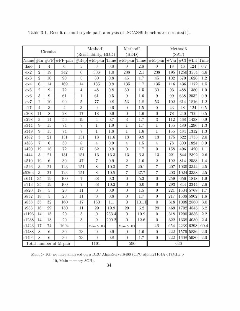
Table 3.1. Result of multi-cycle path analysis of ISCAS89 benchmark circuits(1).
CircuitsMethod1
(Reachability, BDD)Method2(BDD)
Method3(SAT)
Name #In #FF #FF-pair #Rep #M-pair Time #M-pair Time #M-pair #Var #Cl #Lit Timedaio 1 4 6 5 0 0.8 0 2.8 0 18 46 124 0.7ex2 2 19 342 6 306 1.0 238 2.1 238 195 1250 3554 4.6ex3 2 10 90 5 80 0.8 45 1.7 45 102 570 1626 1.2ex4 6 14 169 14 135 0.9 135 1.7 135 116 436 1172 1.5ex5 2 9 72 4 48 0.8 30 1.5 30 93 488 1380 1.0ex6 5 9 61 1 61 0.5 9 1.6 9 99 638 2032 0.9ex7 2 10 90 5 77 0.8 53 1.8 53 102 614 1816 1.2s27 4 3 4 3 0 0.6 0 1.5 0 23 48 124 0.5s208 11 8 28 17 18 0.9 0 1.6 0 78 240 700 0.5s298 3 14 56 19 4 0.7 3 1.7 3 112 468 1438 0.9s344 9 15 74 7 1 1.9 1 1.7 1 155 480 1296 1.3s349 9 15 74 7 1 1.8 1 1.6 1 155 484 1312 1.3s382 3 21 131 151 13 11.6 13 9.9 13 175 622 1738 2.0s386 7 6 30 8 4 0.9 4 1.5 4 78 500 1824 0.9s420 19 16 72 17 62 0.9 0 1.7 0 158 496 1420 1.1s444 3 21 131 151 13 13.3 13 6.3 13 221 844 2392 2.6s510 19 6 30 47 7 0.9 2 1.6 2 192 814 2588 1.4s526 3 21 123 151 8 10.3 7 20.1 7 207 1030 3344 2.5s526n 3 21 123 151 8 10.5 7 37.7 7 203 1024 3338 2.5s641 35 19 100 7 38 9.3 0 5.3 0 259 656 1818 1.9s713 35 19 100 7 38 10.2 0 6.0 0 293 844 2344 2.6s820 18 5 20 11 0 0.9 0 1.5 0 221 1504 5768 1.7s832 18 5 20 11 0 0.8 0 1.7 0 217 1538 5902 1.6s838 35 32 160 17 150 1.1 0 101.1 0 318 1008 2860 3.0s953 16 29 150 11 29 19.9 29 6.2 29 469 1702 4848 6.2s1196 14 18 20 3 0 253.4 0 10.9 0 318 1290 3856 2.2s1238 14 18 20 3 0 200.2 0 12.6 0 322 1338 4030 2.4s1423 17 74 1694 — Mem > 1G — Mem > 1G — 46 654 2238 6298 60.4s1488 8 6 30 23 0 0.9 0 1.6 0 222 1576 5836 2.0s1494 8 6 30 23 0 0.8 0 1.7 0 222 1608 5980 2.0Total number of M-pair 1101 590 636
Mem > 1G: we have analyzed on a DEC AlphaServer8400 (CPU alpha21164A 617MHz ×10, Main memory 8GB).
34
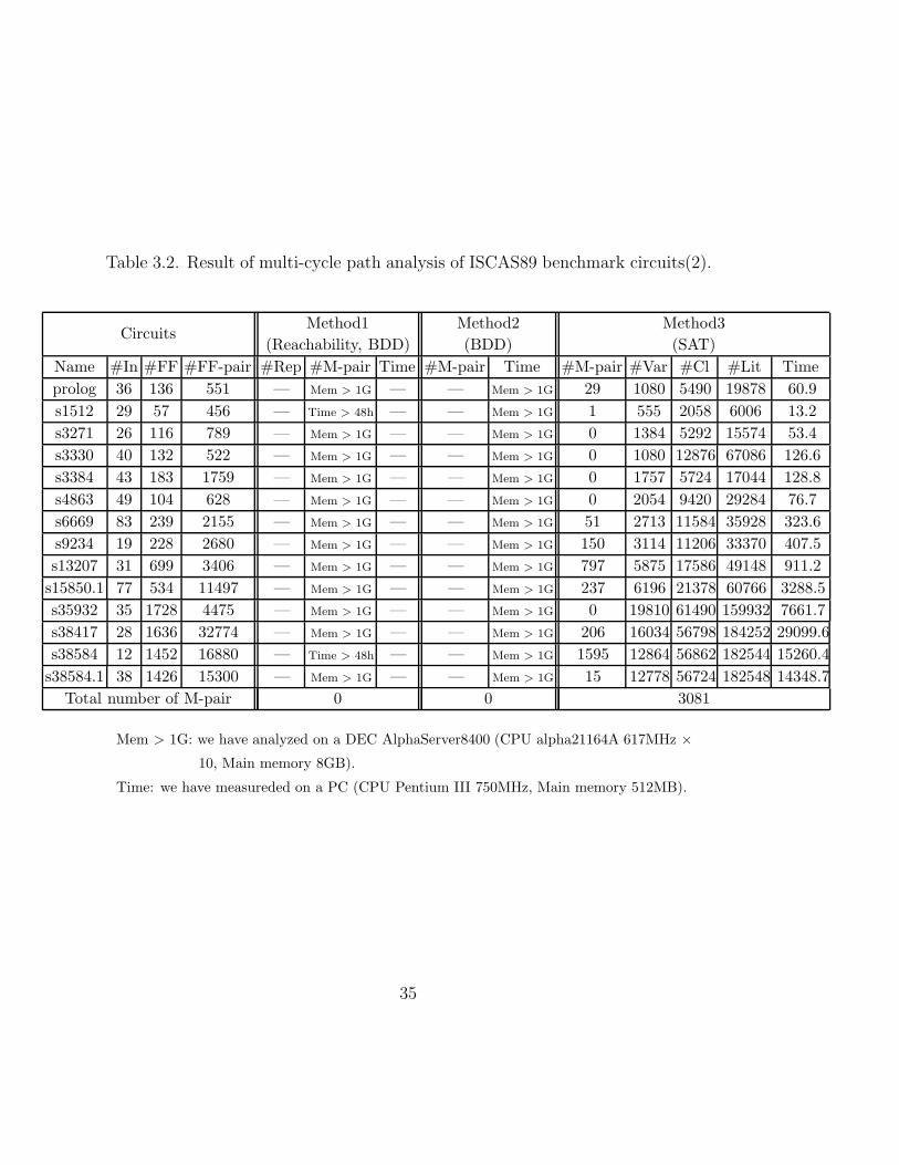
Table 3.2. Result of multi-cycle path analysis of ISCAS89 benchmark circuits(2).
CircuitsMethod1
(Reachability, BDD)Method2(BDD)
Method3(SAT)
Name #In #FF #FF-pair #Rep #M-pair Time #M-pair Time #M-pair #Var #Cl #Lit Timeprolog 36 136 551 — Mem > 1G — — Mem > 1G 29 1080 5490 19878 60.9s1512 29 57 456 — Time > 48h — — Mem > 1G 1 555 2058 6006 13.2s3271 26 116 789 — Mem > 1G — — Mem > 1G 0 1384 5292 15574 53.4s3330 40 132 522 — Mem > 1G — — Mem > 1G 0 1080 12876 67086 126.6s3384 43 183 1759 — Mem > 1G — — Mem > 1G 0 1757 5724 17044 128.8s4863 49 104 628 — Mem > 1G — — Mem > 1G 0 2054 9420 29284 76.7s6669 83 239 2155 — Mem > 1G — — Mem > 1G 51 2713 11584 35928 323.6s9234 19 228 2680 — Mem > 1G — — Mem > 1G 150 3114 11206 33370 407.5s13207 31 699 3406 — Mem > 1G — — Mem > 1G 797 5875 17586 49148 911.2s15850.1 77 534 11497 — Mem > 1G — — Mem > 1G 237 6196 21378 60766 3288.5s35932 35 1728 4475 — Mem > 1G — — Mem > 1G 0 19810 61490 159932 7661.7s38417 28 1636 32774 — Mem > 1G — — Mem > 1G 206 16034 56798 184252 29099.6s38584 12 1452 16880 — Time > 48h — — Mem > 1G 1595 12864 56862 182544 15260.4s38584.1 38 1426 15300 — Mem > 1G — — Mem > 1G 15 12778 56724 182548 14348.7
Total number of M-pair 0 0 3081
Mem > 1G: we have analyzed on a DEC AlphaServer8400 (CPU alpha21164A 617MHz ×10, Main memory 8GB).
Time: we have measureded on a PC (CPU Pentium III 750MHz, Main memory 512MB).
35
s641, s713 and s838 can not be found by Method2 and Method3, and the total
number of paths is small on Method2 and Method3 for detected circuits. The
total number of ”#M-pair” with Method 1 is 1101, and those with Method 2 and 3
are 590 and 3717. Table 3.1 shows that more than half of M-pairs can be detected
under the assumption where all states are reachable. Note that Method 3 can
detect some of M-pairs of s1423, prolog, s1512, s6669, s9234, s13207, s15850.1,
s38417, s38584 and s38584.1 which include the node explosion of BDDs.
3.6.2 Results on Sample Circuits
We have applied our SAT-based method and the BDD-based method in [16] to
several circuits which are designed in our laboratory: prime250 (a prime num-
ber generator which computes prime numbers less than 250, about 400 gates),
s-div8 (an 8-bit sequential divider, about 500 gates), prime999 (a prime num-
ber generator which computes prime numbers less than 999, about 400 gates),
bezier8 (an 8-bit bezier curve generator, about 900 gates), forsen (an edge de-
tection circuit for image processing, about 900 gates), pcpu16 (a 16-bit pipelined
processor, about 9,000 gates), mul64 (a circuit including a 64-bit combinational
adder array multiplier, about 47,000 gates), SpchRecog (an HMM-based speech
recognition circuit, about 40,000 gates) [17], EyeTracking (an eye tracking cir-
cuit, about 45,000 gates) [15]. These circuits have been designed to include
multi-cycle paths. Multi-cycle paths of forsen are introduced to meet the clock
constraints, those of SpchRecog and EyeTracking are introduced for memory ac-
cess constraints. Multi-cycle paths of mul64 are introduced for experiments. We
have found multi-cycle flip-flop pairs on all circuits except pcpu16 by Method3.
pcpu16 may not include any multi-cycle flip-flop pairs since the circuit consists
of pipelined modules. Table 3.3 shows the statistics. Almost all circuits, BDD-
based methods suffer from memory overflow or time-overflow. We used SATO as
a SAT prover if not specified. For SpchRecog and EyeTracking, we should use
GRASP to overcome the number of flip-flops more than 1000.
Most of multi-cycle flip-flop pairs detected by the analysis relate to counters
controlling the hardware loop and the structure of the circuit, in which the value
changes are controlled by wait states.
36
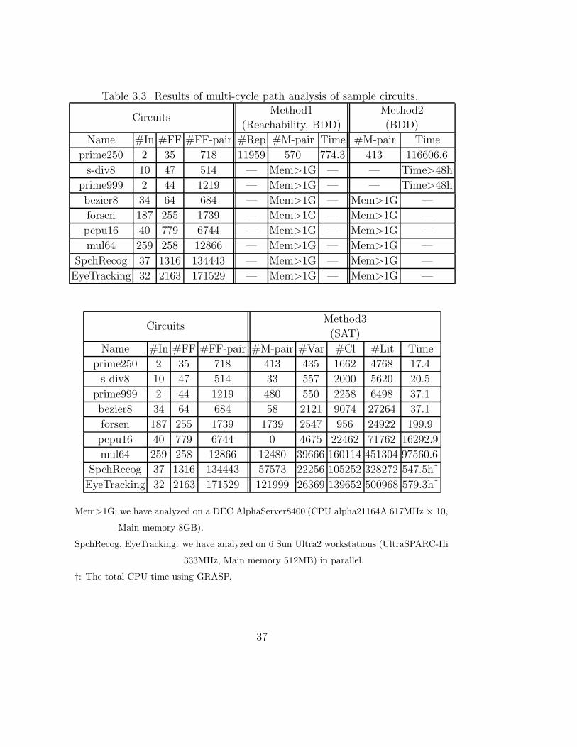
Table 3.3. Results of multi-cycle path analysis of sample circuits.
CircuitsMethod1
(Reachability, BDD)
Method2
(BDD)
Name #In #FF #FF-pair #Rep #M-pair Time #M-pair Time
prime250 2 35 718 11959 570 774.3 413 116606.6
s-div8 10 47 514 — Mem>1G — — Time>48h
prime999 2 44 1219 — Mem>1G — — Time>48h
bezier8 34 64 684 — Mem>1G — Mem>1G —
forsen 187 255 1739 — Mem>1G — Mem>1G —
pcpu16 40 779 6744 — Mem>1G — Mem>1G —
mul64 259 258 12866 — Mem>1G — Mem>1G —
SpchRecog 37 1316 134443 — Mem>1G — Mem>1G —
EyeTracking 32 2163 171529 — Mem>1G — Mem>1G —
CircuitsMethod3
(SAT)
Name #In #FF #FF-pair #M-pair #Var #Cl #Lit Time
prime250 2 35 718 413 435 1662 4768 17.4
s-div8 10 47 514 33 557 2000 5620 20.5
prime999 2 44 1219 480 550 2258 6498 37.1
bezier8 34 64 684 58 2121 9074 27264 37.1
forsen 187 255 1739 1739 2547 956 24922 199.9
pcpu16 40 779 6744 0 4675 22462 71762 16292.9
mul64 259 258 12866 12480 39666 160114 451304 97560.6
SpchRecog 37 1316 134443 57573 22256 105252 328272 547.5h†
EyeTracking 32 2163 171529 121999 26369 139652 500968 579.3h†
Mem>1G: we have analyzed on a DEC AlphaServer8400 (CPU alpha21164A 617MHz × 10,
Main memory 8GB).
SpchRecog, EyeTracking: we have analyzed on 6 Sun Ultra2 workstations (UltraSPARC-IIi
333MHz, Main memory 512MB) in parallel.
†: The total CPU time using GRASP.
37
3.6.3 Effects of Thresholds for Inserting New Variables
We have tested properties of thresholds which are used to insert new variables
in our algorithm. We have experimented with two medium size circuits and two
large circuits in Table 3.1 and Table 3.3.
Table 3.4 shows statistics of multi-cycle path detection of s1423, mul16, mul64
and SpchRecog. In the table, “Threshold: a, b, c, d” denote “XOR-level”, “OR-
level”, “AND-level” and “NOT-level” in Figure 3.2. Since XOR gates grow the
size of CNF formulae heavily as we described in Section 3.5.1, “XOR-level” is set
to 1. Note that our algorithm with (1, 1, 1, 2) inserts variables for all logic gates.
From these tables, we can see the effect of the threshold values on the size of
CNF formulae and the elapsed CPU time. The statistics show that the reduction
of the size of CNF formula does not always contribute to reduce the time for
analysis. The analysis with thresholds (1, 9, 9, 10) need the shortest CPU time
for medium size circuits, but the analysis need much time or memory than that
with (1, 4, 4, 5) for large circuits. The analysis with (1, 4, 4, 5) finished in all
cases with reasonable time and memory.
38
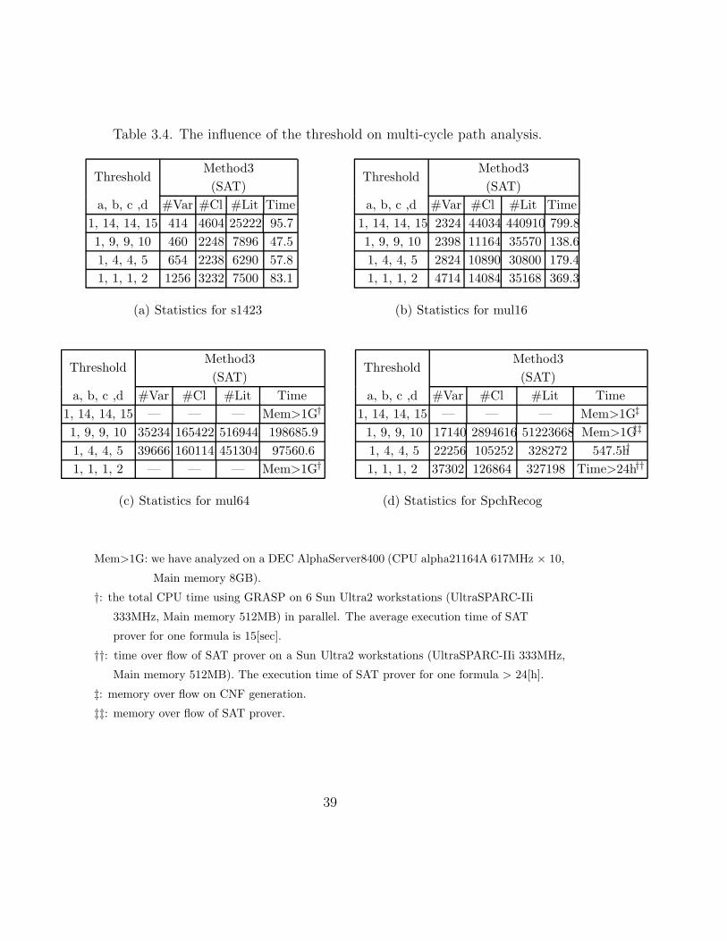
Table 3.4. The influence of the threshold on multi-cycle path analysis.
ThresholdMethod3(SAT)
ThresholdMethod3(SAT)
a, b, c ,d #Var #Cl #Lit Time a, b, c ,d #Var #Cl #Lit Time1, 14, 14, 15 414 4604 25222 95.7 1, 14, 14, 15 2324 44034 440910 799.81, 9, 9, 10 460 2248 7896 47.5 1, 9, 9, 10 2398 11164 35570 138.61, 4, 4, 5 654 2238 6290 57.8 1, 4, 4, 5 2824 10890 30800 179.41, 1, 1, 2 1256 3232 7500 83.1 1, 1, 1, 2 4714 14084 35168 369.3
(a) Statistics for s1423 (b) Statistics for mul16
ThresholdMethod3(SAT)
ThresholdMethod3(SAT)
a, b, c ,d #Var #Cl #Lit Time a, b, c ,d #Var #Cl #Lit Time1, 14, 14, 15 — — — Mem>1G† 1, 14, 14, 15 — — — Mem>1G‡
1, 9, 9, 10 35234 165422 516944 198685.9 1, 9, 9, 10 17140 2894616 51223668 Mem>1G‡‡
1, 4, 4, 5 39666 160114 451304 97560.6 1, 4, 4, 5 22256 105252 328272 547.5h†
1, 1, 1, 2 — — — Mem>1G† 1, 1, 1, 2 37302 126864 327198 Time>24h††
(c) Statistics for mul64 (d) Statistics for SpchRecog
Mem>1G: we have analyzed on a DEC AlphaServer8400 (CPU alpha21164A 617MHz × 10,
Main memory 8GB).
†: the total CPU time using GRASP on 6 Sun Ultra2 workstations (UltraSPARC-IIi
333MHz, Main memory 512MB) in parallel. The average execution time of SAT
prover for one formula is 15[sec].
††: time over flow of SAT prover on a Sun Ultra2 workstations (UltraSPARC-IIi 333MHz,
Main memory 512MB). The execution time of SAT prover for one formula > 24[h].
‡: memory over flow on CNF generation.
‡‡: memory over flow of SAT prover.
39
3.7. Conclusion
In this chapter, we have presented multi-cycle path detection method based on
propositional satisfiability and shown experimental results.
The method reduces multi-cycle path detection problems into SAT problems.
In the conversion from multi-level circuits into CNF formulae, the method adap-
tively inserts intermediate variables to reduce the size of CNF formulae which are
given to a SAT prover.
The SAT-based algorithm enables us to apply multi-cycle path analysis to
large circuits that can not be analyzed with the symbolic state traversal based
algorithm.
We have applied our method to ISCAS89 benchmarks and other sample cir-
cuits. Experimental results show the improvement on the manipulatable size of
circuits by using satisfiability.
The problem is that the SAT-based algorithm can only detect a subset of
multi-cycle paths detectable by the algorithm based on the symbolic state traver-
sal of FSMs. We should develop SAT-based manipulations of reachable states.
40
Chapter 4
Application of Multi-Cycle Path
Analysis to Logic Synthesis
4.1. Area Optimization with Information of Multi-
Cycle Paths
The number of allowable clock cycles for each path is computed in the multi-
cycle paths detection, and the number is useful for optimizing circuits in logic
synthesis. We describe the area optimization of circuits with the information of
allowable clock cycles of paths.
In general, the area of circuits becomes small as the delay time of circuits
becomes long. This is trade-off between the area and the delay time of circuits.
Hence, when a circuit includes many multi-cycle paths the area of the circuit
may be reduced. Circuits which include multi-cycle paths are optimized by the
following process.
1. Multi-cycle path detection:
we detect multi-cycle paths with the method proposed in this thesis.
2. Multi-cycle path specification:
we specify the multi-cycle paths for the logic synthesis.
3. Multi-cycle path constrained synthesis:
we optimize the circuit under the timing constraints which are based on
41
multi-cycle paths.
[Example]
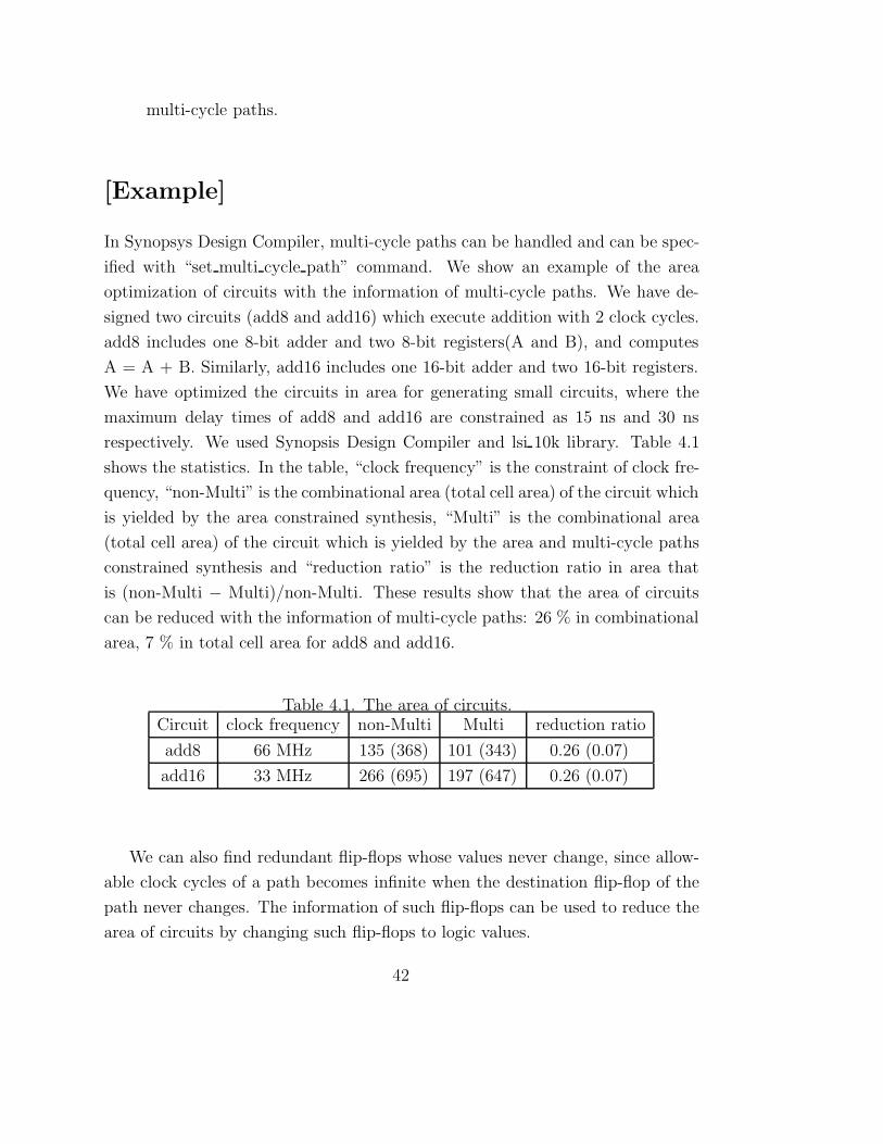
In Synopsys Design Compiler, multi-cycle paths can be handled and can be spec-
ified with “set multi cycle path” command. We show an example of the area
optimization of circuits with the information of multi-cycle paths. We have de-
signed two circuits (add8 and add16) which execute addition with 2 clock cycles.
add8 includes one 8-bit adder and two 8-bit registers(A and B), and computes
A = A + B. Similarly, add16 includes one 16-bit adder and two 16-bit registers.
We have optimized the circuits in area for generating small circuits, where the
maximum delay times of add8 and add16 are constrained as 15 ns and 30 ns
respectively. We used Synopsis Design Compiler and lsi 10k library. Table 4.1
shows the statistics. In the table, “clock frequency” is the constraint of clock fre-
quency, “non-Multi” is the combinational area (total cell area) of the circuit which
is yielded by the area constrained synthesis, “Multi” is the combinational area
(total cell area) of the circuit which is yielded by the area and multi-cycle paths
constrained synthesis and “reduction ratio” is the reduction ratio in area that
is (non-Multi − Multi)/non-Multi. These results show that the area of circuits
can be reduced with the information of multi-cycle paths: 26 % in combinational
area, 7 % in total cell area for add8 and add16.
Table 4.1. The area of circuits.Circuit clock frequency non-Multi Multi reduction ratio
add8 66 MHz 135 (368) 101 (343) 0.26 (0.07)
add16 33 MHz 266 (695) 197 (647) 0.26 (0.07)
We can also find redundant flip-flops whose values never change, since allow-
able clock cycles of a path becomes infinite when the destination flip-flop of the
path never changes. The information of such flip-flops can be used to reduce the
area of circuits by changing such flip-flops to logic values.
42
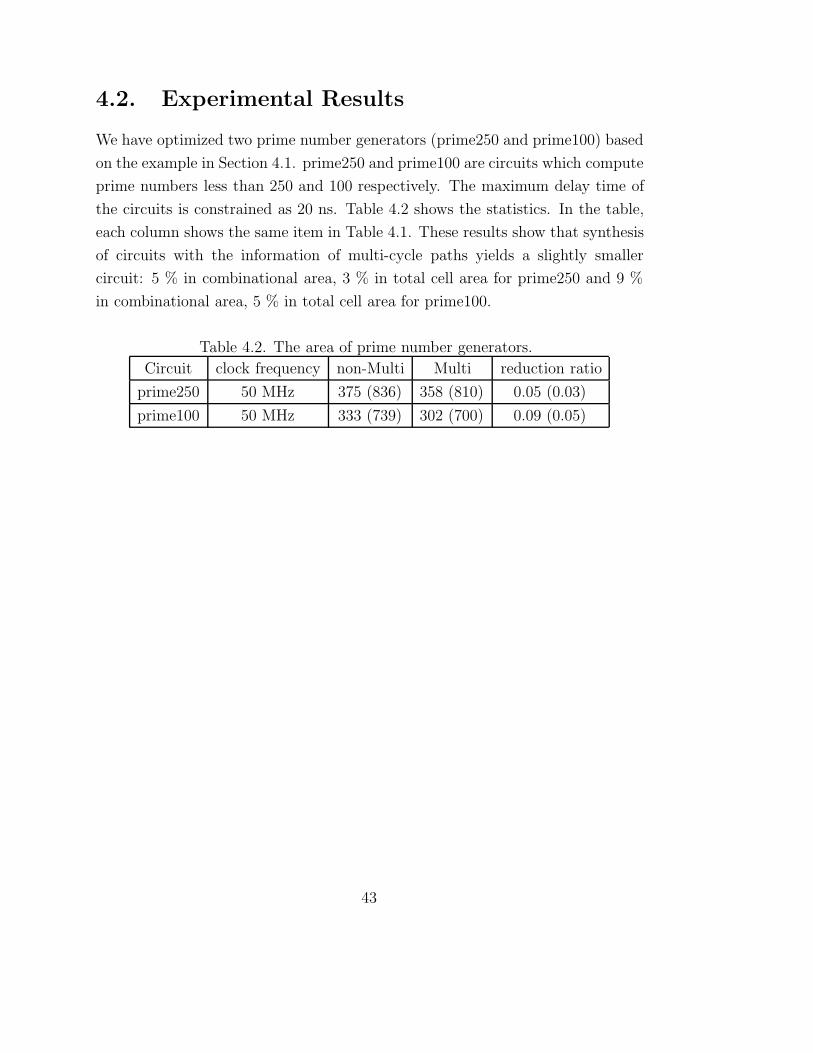
4.2. Experimental Results
We have optimized two prime number generators (prime250 and prime100) based
on the example in Section 4.1. prime250 and prime100 are circuits which compute
prime numbers less than 250 and 100 respectively. The maximum delay time of
the circuits is constrained as 20 ns. Table 4.2 shows the statistics. In the table,
each column shows the same item in Table 4.1. These results show that synthesis
of circuits with the information of multi-cycle paths yields a slightly smaller
circuit: 5 % in combinational area, 3 % in total cell area for prime250 and 9 %
in combinational area, 5 % in total cell area for prime100.
Table 4.2. The area of prime number generators.
Circuit clock frequency non-Multi Multi reduction ratio
prime250 50 MHz 375 (836) 358 (810) 0.05 (0.03)
prime100 50 MHz 333 (739) 302 (700) 0.09 (0.05)
43

Chapter 5
Conclusion
In this thesis, we have formalized multi-cycle paths and proposed two detection
methods of multi-cycle paths, one is based on a symbolic state traversal of FSMs
and the other is based on propositional satisfiability.
In Chapter 2, we have proposed a method to detect the multi-cycle paths.
Multi-cycle paths exist when input and output flip-flops of the paths are guarded
with wait states, and the delay time of the path can be greater than the clock
period. Hence, we should decide the clock period under the constraint where the
delay of the path is smaller than the clock period multiplied by the maximum
allowable clock cycle. In the detection of multi-cycle paths, we use the symbolic
state traversal to obtain the state sets with update cycle more than 2. We have
applied the detection method to ISCAS benchmarks and found multi-cycle paths
on 22 circuits in 30 finite state machine benchmarks. Multi-cycle path analysis
can be applied to maximize the clock frequency of sequential logic circuits. Since
our method includes BDD manipulations, the applicable circuit size is restricted
by the memory size for manipulating BDD’s. At present technology, circuits
including 50-100 flip-flops can be manipulated by the method.
In Chapter 3, we have presented multi-cycle path detection method based on
propositional satisfiability and shown experimental results. The method reduces
multi-cycle path detection problems into SAT problems. In the conversion from
multi-level circuits into CNF formulae, the method adaptively inserts intermedi-
ate variables to reduce the size of CNF formulae which are given to a SAT prover.
The SAT-based algorithm enables us to apply multi-cycle path analysis to large
45
circuits that can not be analyzed with the algorithm based on the symbolic state
traversal of FSMs. We have applied our method to ISCAS89 benchmarks and
other sample circuits. Experimental results show the improvement on the manip-
ulatable size of circuits by using satisfiability. The problem is that the SAT-based
algorithm can only detect a subset of multi-cycle paths detectable by the sym-
bolic execution based algorithm. We should develop SAT-based manipulations of
reachable states.
In Chapter 4, we have shown logic optimization with the information of de-
tected multi-cycle paths. The informations on multi-cycle paths can be used
in logic optimization to reduce the number of gates and the size of gates with
considering allowable clock cycles of each path.
Multi-cycle path analysis is important for the correct timing analysis, and the
multi-cycle path detection method proposed in this thesis contributes to improve
the accuracy of timing analysis. However, in sequential circuits, there still exist
paths which are sensitizable but do not affect the clock period. For example, if
the value of a flip-flop rout is not referred at some clock cycle, then the signal to
rout may not be propagated at the cycle. In other words, there may be a 3-cycle
path including an intermediate flip-flop whose value is not referred in some clock
cycle. For the precise timing analysis, we should develop manipulation methods
of such paths.
46

Acknowledgements
I would like to express my sincere appreciation to Professor Katsumasa Watanabe
of Nara Institute of Science and Technology for his continuous guidance, helpful
suggestions, accurate criticisms and encouragement for this research.
I would also like to appreciate Professor Hideo Fujiwara and Professor Akira
Fukuda of Nara Institute of Science and Technology for their invaluable comments
and helpful suggestions concerning this thesis.
I would also like to express my gratitude to Associate Professor Shinji Kimura
of Nara Institute of Science and Technology who introduced me to this research
field, and has been giving me invaluable suggestions, accurate criticisms and
encouragement through this research.
I would also like to express my thanks to Lecturer Kazuyoshi Takagi of Nagoya
University for his valuable discussions and comments.
I would also like to thank Research Associate Takashi Horiyama and Research
Associate Masaki Nakanishi of Nara Institute of Science and Technology for their
discussions and helpful support throughout this research.
I also wish to express my thanks to Associate Professor Satoshi Yamane of
Kagoshima University for his helpful suggestions and encouragement when I was
an under graduate student of Shimane University.
I also wish to thank Mr. Shinji Maruoka of Hitachi, Ltd. for his helpful
discussions when he was a master course student of Nara Institute of Science and
Technology.
Thanks are due to all members of Watanabe Laboratory for their discussions
and helpful comments.
Lastly, I thank my parents for their patience, support and encouragement.
47

References
[1] P. Ashar, S. Dey, and S. Malik. “Exploiting Multicycle False Paths in the
Performance Optimization of Sequential Logic Circuits”. IEEE Transactions
on CAD, vol-14(9), pp. 1067–1075, Sep. 1995.
[2] J. Benkowski, E.V. Meersch, L.J.M. Claesen, and H. DE MAN. “Timing
Verification Using Statistically Sensitizing Path”. IEEE Transactions on
CAD, vol-9(10), pp. 1073–1084, Oct. 1990.
[3] A. Biere, A. Cimatti, E. M. Clarke, M. Fujita, and Y. Zhu. “Symbolic
Model Checking using SAT procedures instead of BDDs”. In of 36th Design
Automation Conference (DAC’99), 1999.
[4] F. Brglez, D. Bryan, and K. Kozminski. “Combinational Profiles of Se-
quential Benchmark Circuits”. In IEEE 1989 International Symposium on
Circuits and Systems Proceedings, pp. 1929–1934, May 1989.
[5] R.E. Bryant. “Symbolic Boolean Manipulation with Ordered Binary-
Decision Diagrams”. ACM Computing Surveys, vol.24(3), pp. 293–318, Sep.
1992.
[6] H.C. Chen and D.H. Du. “Path Sensitization in Critical Path Problem”. In
Proc. of International Conference on Computer Aided Design (ICCAD’91),
pp. 208–221, 1991.
[7] O. Coudert, C. Berthet, and J. C Madre. “Verification of Sequential Ma-
chines Based on symbolic Execution”. In LNCS 407, Automatic Verification
Methods for Finite State Systems, pp. 365–373, Sep. 1989.
49
[8] M. Davis and H. Putnam. “A Computing Procedure for Quantification The-
ory”. Journal of the Association for Computing Machinery, 7, pp.201–215,
1960.
[9] M. Fujita and E. M. Clarke. “Application of BDD to CAD for digital sys-
tems”. Information Processing, Vol. 34(5), pp. 609–616, May 1993.
[10] Anurag P. Gupta and Daniel P. Siewiorek. “Automated Multi-Cycle Sym-
bolic Timing Verification of Microprocessor-based Designs”. In Proc. of 31st
Design Automation Conference (DAC’94), pp. 113–119, 1994.
[11] J.E. Hopcroft and J.D. Ullman. “Introduction to Automata Theory, Lan-
guages and Computation”. Addison-Wesley, 1979.
[12] D. S. Johnson and editors M. A. Trick. “The second DIMACS implementa-
tion challenge”. In DIMACS Series in Discrete Mathematics and Theoretical
Computer Science, 1993, (see http://dimacs.rutgers.edu/Challenges/).
[13] Tracy Larrabee. “Test Pattern Generation Using Boolean Satisfiability”.
IEEE Transaction on Computer-Aided Design, pp. 4–15, Jan. 1992.
[14] P. C. McGeer, A. Saldanha, R. K. Brayton, and A. Sangiovanni-Vincentelli.
“Delay Models and Exact Timing Analysis”. In Logic Synthesis and Opti-
mization, Kluwer Academic Publishers, pp. 167–189, 1993, ed. T. Sasao.
[15] Kazuhiro Nakamura, Masaki Nakanishi, Takashi Horiyama, Masato Suzuhi,
Shinji Kimura, and Katsumasa Watanabe. “Real-time Eye Tracking LSI
for Eye-based Interface”. In Proc. of 4th System LSI Biwako Workshop,
pp. 267–270, 2000.
[16] Kazuhiro Nakamura, Kazuyoshi Takagi, Shinji Kimura, and Katsumasa
Watanabe. “Waiting False Path Analysis of Sequential Logic Circuits for
Performance Optimization”. In Proc. of International Conference on Com-
puter Aided Design (ICCAD’98), pp. 392-395, 1998.
[17] Kazuhiro Nakamura, Qiang Zhu, Shinji Maruoka, Takashi Horiyama, Shinji
Kimura, and Katsumasa Watanabe. “Speech Recognition Chip for Monosyl-
50
lables”. In Proc. of Asia and South Pacific Design Automation Conference
(ASP-DAC 2001), pp. 396-399, 2001.
[18] D. Plaisted and S. Greenbaum. “A Structure-Preserving Clause Form Trans-
lation”. Journal of Symbolic Computation, 2, pp. 293–304, 1986.
[19] J. Silva and K. Sakallah. “GRASP: A Search Algorithm for Propositional
Satisfiability”. IEEE Transactions on Computers, pp. 506–521, May 1999.
[20] L. G. Silva, J. P. M. Silva, L. M. Silveira, and K. A. Sakallah. “Timing Anal-
ysis Using Propositional Satisfiability”. In IEEE International Conference
on Electronics, Circuits and Systems, 1998.
[21] S. Yang. “Logic Synthesis and Optimization Benchmarks User Guide”. In
Technical Report 1991-IWLS-UG-Saeyang, 1991.
[22] H. Zhang. “SATO: An Efficient Propositional Prover”. In of International
Conference on Automated Deduction’97, pp. 272–275, 1997.
51

52
List of Publications
Journal Papers
1. Kazuhiro Nakamura, Shinji Kimura, Kazuyoshi Takagi and Katsumasa
Watanabe, “Timing Verification of Sequential Logic Circuits Based on Con-
trolled Multi-clock Path Analysis,” IEICE Transactions on Fundamentals,
Vol. E81-A, No. 12, pp. 2515-2520, December 1998.
2. Kazuhiro Nakamura, Shinji Maruoka, Shinji Kimura and KatsumasaWatan-
abe, “Multi-Cycle Path Detection Based on Propositional Satisfiability with
CNF Simplification Using Adaptive Variable Insertion,” IEICE Transac-
tions on Fundamentals, Vol. E83-A, No. 12, pp. 2600-2607, December 2000.
International Conferences
1. Kazuhiro Nakamura, Kazuyoshi Takagi, Shinji Kimura and Katsumasa
Watanabe, “Waiting False Path Analysis of Sequential Logic Circuits for
Performance Optimization,” Proceedings of IEEE/ ACM International Con-
ference on Computer Aided Design 1998, pp. 392-395, November 1998.
2. Kazuhiro Nakamura, Shinji Maruoka, Shinji Kimura and KatsumasaWatan-
abe, “Multi-Clock Path Analysis Using Propositional Satisfiability,” Pro-
ceedings of Asia and South Pacific Design Automation Conference 2000,
pp. 81-86, January 2000.
3. Kazuhiro Nakamura, Qiang Zhu, Shinji Maruoka, Takashi Horiyama, Shinji
Kimura and Katsumasa Watanabe, “Speech Recognition Chip for Monosyl-
lables,” Proceedings of Asia and South Pacific Design Automation Confer-
ence 2001, pp. 396-399, January 2001.
4. Kazuhiro Nakamura, Qiang Zhu, Shinji Maruoka, Takashi Horiyama, Shinji
Kimura and Katsumasa Watanabe, “A Real-time 64-Monosyllable Recogni-
tion LSI with Learning Mechanism,” Proceedings of Asia and South Pacific
Design Automation Conference 2001, pp. 31-32, January 2001.
53
Technical Reports
1. Kazuhiro Nakamura, Shinji Kimura, Kazuyoshi Takagi and Katsumasa
Watanabe, “Waiting False Path Analysis of Sequential Logic Circuits,”
Technical Report of IEICE, VLD97-132, ICD97-237, pp. 71-77, March 1998,
(in Japanese).
2. Kazuhiro Nakamura, Shinji Maruoka, Shinji Kimura and KatsumasaWatan-
abe, “Multi-Clock Path Analysis Based on Propositional Satisfiability,”
Technical Report of IEICE, VLD99-82, ICD99-211, FTS99-60, pp. 55-62,
November 1999, (in Japanese).
3. Kazuhiro Nakamura, Shinji Maruoka, Shinji Kimura and KatsumasaWatan-
abe, “State Enumeration Based on Propositional Satisfiability,” Technical
Report of IEICE, VLD2000-26, CAS200-17,DSP2000-38, pp. 123-130, June
2000, (in Japanese).
4. Kazuhiro Nakamura, Qiang Zhu, Shinji Maruoka, Takashi Horiyama, Shinji
Kimura and Katsumasa Watanabe, “Design and Implementation of LSI for
Speech Recognition with Learning Mechanism Using C Language,” Techni-
cal Report of IEICE, VLD2000-90, ICD200-147, FTS2000-55, pp. 125-130,
November 2000, (in Japanese).
5. Kazuhiro Nakamura, Masaki Nakanishi, Takashi Horiyama, Masato Suzuhi,
Shinji Kimura and Katsumasa Watanabe, “Real-time Eye Tracking LSI
for Eye-based Interface,” 4th System LSI Biwako Workshop, pp. 267-270,
November 2000, (in Japanese).
6. Kazuhiro Nakamura, Shinji Kimura, Kazuyoshi Takagi and Katsumasa
Watanabe, “Timing Verification Using Waiting False Path Analysis of Gen-
eral Conference of IEICE, A-3-8, pp. 94, March 1998, (in Japanese).
7. Shinji Maruoka, Kazuhiro Nakamura, Shinji Kimura and KatsumasaWatan-
abe, “Propositional Satisfiability for Multi-Level Logic Circuits and its Ap-
plication to Multi-Clock Path Analysis,” Society Conference of IEICE, A-
3-8, pp. 51, September 1999, (in Japanese).
54
8. Kazuhiro Nakamura, Qiang Zhu, Shinji Maruoka, Takashi Horiyama, Shinji
Kimura and Katsumasa Watanabe, “Speaker Independent Speech Recogni-
tion Circuit with Learning Circuit Interface,” Society Conference of IEICE,
A-3-13, pp. 80, October 2000, (in Japanese).
Other Publications
International Conference
1. Kazuhiro Nakamura and Satoshi Yamane, “Formal Verification of Real-
Time Software by Symbolic Model Checker,” Proceedings of International
Conference on Application of Concurrency to System Design 1998, pp. 99-
108, March 1998.
Technical Reports
1. Satoshi Yamane and Kazuhiro Nakamura, “Symbolic Model-Checking Ver-
ification of Timed Automata Based on Region Graph Method,” Technical
Report of IEICE, FTS96-28, pp. 1-8, June 1996, (in Japanese).
2. Kazuhiro Nakamura and Satoshi Yamane, “Real-time Symbolic Model-
Checking Method Based on Approximations by BDD and DBM,” 10th
Karuizawa Workshop on Circuits and Systems, pp. 77-82, April 1997, (in
Japanese).
3. Kenichi Takahashi, Kazuhiro Nakamura and Satoshi Yamane, “Formal Ver-
ification of Speed-Independent Circuit Based on BDD,” General Conference
of IEICE, D-10-2, pp. 231, March 1997, (in Japanese).
4. Kazuhiro Nakamura and Satoshi Yamane, “Real-time Symbolic Model-
Checking Method Based on Approximations by BDD and DBM,” General
Conference of IEICE, D-10-3, pp. 232, March 1997, (in Japanese).
55