Embed Size (px)
Citation preview
University of Ljubljana
Faculty of Mathematics and Physics
Andrej Studen
Compton Camera with Position-Sensitive Silicon
Detectors
Doctoral Thesis
Supervisor: Prof. Dr. Marko Mikuz
Ljubljana, 2005


Univerza v Ljubljani
Fakulteta za matematiko in fiziko
Andrej Studen
Comptonska kamera s krajevno locljivimi silicijevimi
detektorji
Doktorska disertacija
Mentor: prof. dr. Marko Mikuz
Ljubljana, 2005


Ta doktorat ne bi nastal brez izdatne pomoci ljudi okrog mene. Na prvem mestu je mentor in
sef Marko Mikuz, ki je znal kriticno presoditi moje ideje in me uspesno voditi do uspesnega
zakljucka. Posebna zahvala gre Dejanu Zontarju za motivacijo pisanju, skrbno branje in
opozorila na neskladja in slogovne napake v doktorskem delu. Pri projektu Comptonska
kamera sta pomembno sodelovala se Vladimir Cindro in Erik Margan. Za prijetno delovno
vzdusje bi se rad zahvalil tudi vsem ostalim sodelavcem z Odseka za eksperimentalno fiziko
osnovnih delcev Instituta Jozef Stefan.
I should also like to thank people from all over the world who participated in this Compton
camera study. First there are the project master minds Neal Clinthorne and Les Rogers
from University of Michigan. During my stays in Michigan there were Lisha, Sang-June
and Sam who helped to push things along. When working in CERN I had strong support
from local Compton camera group, including the leader of the European part Peter “Failure
is Impossible” Weilhammer, electronic wizard Enrico Chesi, people at bonding lab, Nail
Malakhov with regular soup and tea breaks, and Dirk Meier, currently at IDEAS, who
introduced me to the problematic and invited me to many jogs below the Jura. In Valencia,
special thanks goes to Gabriela Llosa Llacer for sharing restless Sundays figuring Why Things
Don’t Work Like They Are Supposed To and Carlos Lacasta for writing DAQ software. I
will not forget Harris Kagan from Ohio State University, who was an inexhaustible source
of ideas.
Nazadnje bi se zahvalil se prijateljem in druzini, se posebej Kati za moralno podporo in Anji,
da me je naucila, da energija ni vedno sorazmerna masi.

Abstract
Currently, SPECT uses a mechanically collimated (Anger) camera to detect distributionof γ sources. The detection technique, however, suffers from resolution-efficiency trade-offinherent to mechanical collimation. Compton camera principle is a suggested alternativewhich avoids the trade-off. In Compton camera, Compton scattering of emitted photonsis detected in a special scattering detector which replaces the mechanical collimator. Thedirection of the incoming photon is determined from kinematics of Compton scattering.
The thesis describes the development and evaluation of a Compton camera prototype. Theprototype consisted of two sub-detectors: the scattering detector or the scatterer and anabsorber which detects the scattered photons. The scatterer consisted of multiple scatterermodules amplifying the prototype’s efficiency. Each module was equipped with a custom-designed position-sensitive silicon pad sensor coupled to an off-shelf associated electronics.Modules were calibrated and tested. The measurements confirmed energy and spatial reso-lution of the modules suitable for Compton camera.
The imaging heads of the existing SPRINT II imaging ring were the absorber modules ofthe prototype, matching the requirements of Compton camera. The modules were calibratedand tested, and measured results confirmed their eligibility.
The prototype was assembled on a custom designed frame. The scatterer was set in thecenter and three absorber modules formed a semi-ring around the scatterer. The layout ofthe prototype was optimized for imaged objects placed on axis on the semi-ring, providingbest imaging performance with detection of events with the scattering angles around π/2.Data for photons emitted from an on-axis 99mTc point source were measured and from those,the position of the source was reconstructed using a simple back-projection technique.
The determined performance of this simple prototype is similar to the performance of atypical Anger camera. A more refined and improved applications of the principle shouldexcel the performance of present cameras and hence be a competitive tool for future SPECTimaging. A suggested application is a prostate probe, which would enable SPECT imagingof the prostate, an unreachable task for present detection techniques.
Keywords: SPECT, Compton camera, silicon pad detectors, scintillation camera
PACS:
29.30.Kv X- and gamma-ray spectroscopy,29.40.Gx Tracking and position-sensitive detectors,87.58.Ce Single photon emission computed tomography (SPECT).
7

8
Izvlecek
Dandanasnji slikanje izvorov zarkov γ pri SPECT opravi kamera s svincenimi zaslonkami(Angerjeva kamera). Z metodo je nelocljivo povezana izmenjava med izkoristkom in locljivostjo.Tezavo premosti Comptonska kamera; namesto zaslonk ima kamera poseben sipalni detek-tor, v katerem se izsevani fotoni comptonsko sipajo. Smer vpadenga fotona nato doloimo napodlagi kinematike sipanja.
Dokotorska disertacija opisuje razvoj in preizkus delovanja prototipa Comptonske kamere.Prototip je bil sestavljen iz dveh pod-detektorjev: sipalnega detektorja oz. sipalca in ab-sorberja, ki zaznava sipane fotone. Sipalec sestavljajo moduli sipalca; vecje stevilo modulovznantno poveca izkoristek prototipa. Za modul smo razvili posebne krajevno-locljive silici-jeve detektorje z blazinicami in jih sklopili s primerno bralno elektroniko. Umerjeni moduliso pokazali casovno in energijsko locljivost primerno uporabi v Comptonski kameri.
Detektorske glave obroca SPRINT II, namenjenega slikanju sevalcev γ, smo uporabili kotmodule za absorber, saj njihove lastnosti ustrezajo potrebam Comptonske kamere. Modulesmo umerili, rezultati preizkusov pa so potrdili njihovo primernost.
Za prototip je bilo izdelano primerno ogrodje: v centru je bil sipalec, obkrozen s tremimoduli absorberja, ki so tvorili nepopoln obroc. Slikanje je bilo optimizirano za izvorepostavljene v os obroca absorberjev, kar je omogocalo zaznavanje dogodkov s sipalnimi kotiokrog π/2, ki dajejo najnatancnejso sliko izvorov. Prototip smo preizkusli za tockast izvor99mTc postavljen v os obroca in lego izvora rekonstruirali s preprosto projekcijo izmerkovnazaj v prostor izvorov.
Meritve so pokazale, da so lastnosti preprostega prototipa primerljive z lastnostmi sofisti-ciranih Angerjevih kamer. Prototip omogoca stevilne izboljsave, kar nakazuje obetavnostbodocih aplikacij Comptonske kamere. Ena izmed idej je proba za prostato, ki bi omogocalaslikanje prostate s SPECT, cesar trenutna SPECT tehnologija se ne zmore.
Kljucne besede: SPECT, Comptonska kamera, silicijevi detektorji z blazinicami, scinti-
lacijska kamera.
PACS: 29.30.Kv, 29.40.Gx, 87.58.Ce.
9

10

Contents
1 INTRODUCTION 15
1.1 Historical overview . . . . . . . . . . . . . . . . . . . . . . . . . . . . . . . . 16
1.2 Objectives of thesis . . . . . . . . . . . . . . . . . . . . . . . . . . . . . . . . 17
2 Basic principles of Compton Camera operation 19
2.1 Compton camera principle . . . . . . . . . . . . . . . . . . . . . . . . . . . . 19
2.2 Performance parameters of Compton camera . . . . . . . . . . . . . . . . . . 21
2.3 Radio-tracers for SPECT imaging with a Compton camera . . . . . . . . . . 23
2.4 Effect of scatterer energy resolution on angular resolution . . . . . . . . . . . 24
2.5 Doppler broadening . . . . . . . . . . . . . . . . . . . . . . . . . . . . . . . . 25
2.6 Compton scattering probability . . . . . . . . . . . . . . . . . . . . . . . . . 29
2.7 Photo-absorption . . . . . . . . . . . . . . . . . . . . . . . . . . . . . . . . . 32
3 Scatterer 35
3.1 Basics of silicon pad sensor operation . . . . . . . . . . . . . . . . . . . . . . 36
3.2 Front-end electronics . . . . . . . . . . . . . . . . . . . . . . . . . . . . . . . 42
3.2.1 Signal part . . . . . . . . . . . . . . . . . . . . . . . . . . . . . . . . 43
3.2.2 Trigger part . . . . . . . . . . . . . . . . . . . . . . . . . . . . . . . . 46
3.3 Scatterer module assembly . . . . . . . . . . . . . . . . . . . . . . . . . . . . 50
3.3.1 Silicon pad sensor . . . . . . . . . . . . . . . . . . . . . . . . . . . . . 51
3.3.2 ASIC . . . . . . . . . . . . . . . . . . . . . . . . . . . . . . . . . . . . 53
3.3.3 Scatterer module . . . . . . . . . . . . . . . . . . . . . . . . . . . . . 56
11

3.4 Data acquisition and processing . . . . . . . . . . . . . . . . . . . . . . . . . 57
3.4.1 Data acquisition . . . . . . . . . . . . . . . . . . . . . . . . . . . . . . 57
3.4.2 Data processing . . . . . . . . . . . . . . . . . . . . . . . . . . . . . . 58
3.5 Calibration results of scatterer . . . . . . . . . . . . . . . . . . . . . . . . . . 61
3.5.1 Energy resolution . . . . . . . . . . . . . . . . . . . . . . . . . . . . . 62
3.5.2 Spatial resolution . . . . . . . . . . . . . . . . . . . . . . . . . . . . . 67
3.5.3 Trigger properties . . . . . . . . . . . . . . . . . . . . . . . . . . . . . 68
3.6 Conclusion . . . . . . . . . . . . . . . . . . . . . . . . . . . . . . . . . . . . . 73
4 Absorber 75
4.1 SPRINT module . . . . . . . . . . . . . . . . . . . . . . . . . . . . . . . . . 76
4.2 Data acquisition system . . . . . . . . . . . . . . . . . . . . . . . . . . . . . 77
4.3 Module calibration . . . . . . . . . . . . . . . . . . . . . . . . . . . . . . . . 78
4.3.1 Determination of PMT gain . . . . . . . . . . . . . . . . . . . . . . . 79
4.3.2 Determination of impact position . . . . . . . . . . . . . . . . . . . . 81
4.3.3 Energy resolution . . . . . . . . . . . . . . . . . . . . . . . . . . . . . 82
4.3.4 Timing resolution . . . . . . . . . . . . . . . . . . . . . . . . . . . . . 83
4.4 Conclusion . . . . . . . . . . . . . . . . . . . . . . . . . . . . . . . . . . . . . 84
5 Compton camera prototype 87
5.1 Mechanical layout . . . . . . . . . . . . . . . . . . . . . . . . . . . . . . . . . 88
5.2 Prototype parameters related to setup geometry . . . . . . . . . . . . . . . . 89
5.2.1 Setup efficiency . . . . . . . . . . . . . . . . . . . . . . . . . . . . . . 89
5.2.2 Angular resolution . . . . . . . . . . . . . . . . . . . . . . . . . . . . 91
5.3 Data acquisition system . . . . . . . . . . . . . . . . . . . . . . . . . . . . . 94
6 Image reconstruction 99
6.1 Definition of problem . . . . . . . . . . . . . . . . . . . . . . . . . . . . . . . 99
6.2 Back-projection of data from Compton camera . . . . . . . . . . . . . . . . . 102
6.3 Reconstructed images of point sources . . . . . . . . . . . . . . . . . . . . . 103
12

6.4 Conclusion . . . . . . . . . . . . . . . . . . . . . . . . . . . . . . . . . . . . . 108
7 Prototype evaluation 109
7.1 Measured results . . . . . . . . . . . . . . . . . . . . . . . . . . . . . . . . . 110
7.1.1 Spatial resolution . . . . . . . . . . . . . . . . . . . . . . . . . . . . . 110
7.1.2 Efficiency . . . . . . . . . . . . . . . . . . . . . . . . . . . . . . . . . 112
7.1.3 Comparison to Anger camera . . . . . . . . . . . . . . . . . . . . . . 113
7.2 Prostate probe: A possible Compton camera application . . . . . . . . . . . 115
8 Summary 117
9 Povzetek doktorskega dela 119
9.1 Uvod . . . . . . . . . . . . . . . . . . . . . . . . . . . . . . . . . . . . . . . . 119
9.2 Sipalec . . . . . . . . . . . . . . . . . . . . . . . . . . . . . . . . . . . . . . . 121
9.3 Absorber . . . . . . . . . . . . . . . . . . . . . . . . . . . . . . . . . . . . . . 123
9.4 Prototip . . . . . . . . . . . . . . . . . . . . . . . . . . . . . . . . . . . . . . 126
9.5 Rekonstrukcija . . . . . . . . . . . . . . . . . . . . . . . . . . . . . . . . . . 129
9.6 Rezultati in zakljucek . . . . . . . . . . . . . . . . . . . . . . . . . . . . . . . 132
A Sources of electronic noise and their propagation through front-end elec-
tronics 133
B List-mode maximum likelihood expectation maximization 137
C Parameters of data runs used in the thesis 141
D Glossary of frequently used symbols, abbreviations and expressions 143
13

14
Chapter 1
INTRODUCTION
In the field of medical imaging, single photon emission computed tomography (SPECT) isone of the methods enabling in-vivo functional imaging of the tissue. This makes it animportant tool in disease recognition and treatment monitoring. In SPECT the patient isinjected with a radio-tracer that is a disease-specific bio-molecule with chemically bondedradio-active nucleus. A camera sensitive in the energy range of the emitted gamma-raysdetects the spatial distribution of the tracer molecule concentration over time.
Conventional SPECT imagers (Anger cameras) use mechanical collimators to detect thespatial distribution of the radio-tracers. Mechanical collimation couples the spatial resolutionand efficiency of the device in an inverse fashion thus limiting the achievable resolution withacceptable patient-absorbed doses of radiation. To overcome this resolution-efficiency trade-off, ”electronic” collimation, based on Compton scattering kinematics was proposed [TNE74].
In case of electronic collimation the mechanical collimator is replaced with a scatterer, asensor where photons are Compton scattered. A second sensor (the absorber) photo-absorbsthe Compton scattered photons and both sensors operate in coincidence. The kinematics ofCompton scattering is used to determine the scattering angle based on the measured kineticenergy of the Compton electron. All possible directions of incoming photon form a cone,centered on the first interaction point. This leads to an additional ambiguity as opposedto mechanical collimation where a line can be traced from the detector to the source. Themuch higher efficiency of electronic collimation however overcomes this penalty.
The performance of a Compton camera is governed by the following parameters:
• Energy resolution. Either the energy of the recoil electron or the energy of the scatteredphoton have to be known. The detector-material choice should reflect that.
• Spatial resolution. Both detectors should at least match the resolution of a comparableAnger camera.
15

16 1. INTRODUCTION
• Efficiency. The underlying conical ambiguity of Compton imaging requires the Comp-ton camera to have a higher efficiency than its mechanically collimated counterpart forcomparable image quality, which is further discussed in Chapter 7, Section 7.1.3.
• Timing of each sensor. Compton scattering events have to be properly matched tothe interaction of the scattered photon in the absorber. Large discrepancies betweentiming of the individual sensors can lead to event mis-matching and small discrepanciesincrease the amount of random background.
• Image reconstruction. Since data collected on both sensors are only algebraically re-lated to the true tracer density distribution, complex reconstruction techniques arerequired. The complexity of this stage can cause the final image to reflect both thequality of the technique and the quality of the collected data.
• Doppler broadening. Random motion of the bound electron prior to scattering is aninherent limit to the spatial resolution of the reconstructed image. The effect dropswith increasing energy of the initial photons thus electronic collimation favors a choiceof sources with higher energy of initial photons. This is in strong contrast to theAnger camera where photons with higher energy penetrate the collimator and increasebackground.
1.1 Historical overview
It was in the 1950-s that Hal Anger constructed his gamma camera [Ang58]. It was basedon the recently discovered NaI(Tl) scintillator, and the collimation was performed usinglead mechanical collimators. The simplicity of use, relative low cost and simple one-to-oneimaging made it the imager of choice for SPECT. Nevertheless, imaging with Anger camerahas been far from perfect. On average, only one per 10000 photons hitting the detectorarea contributes to the image, others are scattered in the collimator. There is the persistenttrade-off between image resolution and efficiency of the imager. As lead septa get penetrated,imaging degrades with growing photon energy which limits the choice of imaging agents. AllCompton scattered photons in the active detection area cause position ambiguity and haveto be filtered away. Therefore a new detection principles are sought.
The principle of Compton imaging was introduced in the field of gamma-astronomy in 1973[SHS73]. The photon energies are higher than in medical imaging, usually exceeding 1MeV. Since mechanical collimation becomes impractical at high energies, Compton imagingbecomes the method of choice. The Compton Gamma-Ray Observatory (CGRO) was asatelite observatory, orbiting earth between April 5, 1991 and June 4, 2000, and hostedCOMPTEL telescope [GFF+93] which detected location of celestial photon sources usingCompton imaging principle. Several new projects involving Compton telescopes are beinginvestigated [KAS+04, BOA+04].
1.2 Objectives of thesis 17
Compton imaging in nuclear medicine followed, with the introduction in Nature by Toddand Nigthingale in 1974 [TNE74]. It took a while to implement the idea, and the firstprototype was constructed by Singh et al. [Sin83]. Semiconductor scatterer of high puritygermanium (HPGe) was used to measure the recoil electron energy, exhibiting the requiredenergy resolution. The absorber was a conventional Anger camera, with its collimator re-moved . The prototype was used for qualitative studies of the method. Since the absorberwas placed collinearly with the source and the scatterer, many direct hits were observed,causing pile-up in the absorber.
A ring setup of the absorber was introduced by 1993 to avoid direct hits in the absorberby Martin[MKW+93] and co-workers. With the same type of scatterer (HPGe) as for theprevious prototypes (Singh) they performed first imaging tests. The phantoms were simple -a source with or without uniform background. Their spatial resolution was within the orderof magnitude of the available Anger cameras at comparable total efficiency. But taking intoaccount the conical ambiguity their imaging performance was much worse than that of anAnger camera.
A further increase in spatial resolution was achieved with replacement of the HPGe scattererwith a silicon pad sensor[LCH+99]. There are several facts favoring silicon: operation at roomtemperature with negligible loss of energy resolution, excellent spatial resolution, availability,high Compton to photo-absorption ratio, lower Doppler broadening, etc. Similar phantomsas with the first ring prototype were studied, and reconstructed images showed a factor of2 improvement over the HPGe setup. However the performance of the silicon scatterer wasstill far from the desired. A thin silicon layer was used which significantly decreased theefficiency, energy resolution was much lower than expected and timing was not optimized,thus their prototype was still far away from matching Anger camera performance.
1.2 Objectives of thesis
Encouraged by recent development of silicon sensor technology, the thesis concentrates on adevelopment of a Compton camera with position sensitive silicon sensors for medical imaging.As pointed out in [Bla99] there are a number of theoretical advantages of using a Comptoncamera over an Anger camera:
• Higher system sensitivity at required spatial resolution, either improving image at agiven radiation dose uptake by the patient, or decreasing the dose at a given imagequality.
• Better performance at higher gamma-ray energies. Anger camera performance de-creases rapidly with increasing gamma-ray energy due to collimator penetration. Highenergy photons are less likely to scatter in the patient, providing a better data sample.Development of higher energy imaging agents has been hindered by the choice of theimager, and for those Compton imaging could offer a suitable detection technique.

18 1. INTRODUCTION
Maintaining the ring geometry [MKW+93, LCH+99], efforts were concentrated on furtherdevelopment of the silicon sensor array to be used as the scatterer. Silicon pad sensors[WND+96] are an attractive choice for a scatterer of a Compton camera used in medicalimaging, since they offer:
• lower Doppler broadening compared to germanium or other high atomic number semi-conductors (CZT,CdTe),
• excellent spatial resolution,
• adequate energy resolution even at room-temperature,
• high Compton scattering to photo-absorption ratio,
• mature processing techniques,
• robustness.
The goal of the thesis is to construct a Compton camera prototype with a custom developedscatterer module based on silicon pad sensors and associated read-out electronics. Theabsorber is composed of a set of existing modules taken from a single photon ring imager(SPRINT II, [RCS+88]). The prototype is to be tested and its performance evaluated.
Chapter 2
Basic principles of Compton Camera
operation
2.1 Compton camera principle
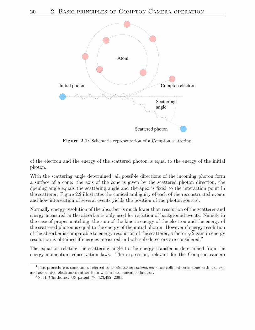
The underlying principle of the Compton camera is a kinematic reconstruction of Comptonscattering. Compton scattering was first described by H.G. Compton in 1923 [Com23] andthe mechanism of the interaction is illustrated in figure 2.1: A photon scatters off a boundelectron, thereby transferring part of its energy and momentum. In Compton scattering,the energy transfer exceeds by far the electron’s binding energy, causing the electron to bereleased from the atom. The direction of the photon is changed and its energy reduced forthe amount transferred to the electron. Only the photon and the electron are involved inthe interaction and the process can be described as a simple two-body problem, yielding arelation of the photon’s scattering angle to the energy transfer.
To reconstruct a Compton scattering event, the Compton camera is made of two sensors. Inthe first sensor, the scatterer, Compton scattering takes place and in the second, the absorber,the scattered photon is absorbed. In the scatterer, three quantities are measured: the timeof the interaction, the point of interaction and the kinetic energy of the released electron.For a successful reconstruction the scattered photon has to escape from the scatterer and beabsorbed in the absorber. The three quantities measured by the absorber are the time ofinteraction, the impact point and the energy of the scattered photon.
The three measurements from each of the sensors are combined to reconstruct the initialphoton direction. Timing information from both sensors is required for coincidence mea-surement, the two interaction positions determine the scattered photon direction and thekinetic energy of the electron is used to determine the scattering angle. Energy of the scat-tered photon can be measured with a low energy resolution and is only used for an off-linebackground rejection. Namely in the case of proper matching, the sum of the kinetic energy
19
20 2. Basic principles of Compton Camera operation
Initial photon
Atom
Compton electron
Scattered photon
angleScattering
Figure 2.1: Schematic representation of a Compton scattering.
of the electron and the energy of the scattered photon is equal to the energy of the initialphoton.
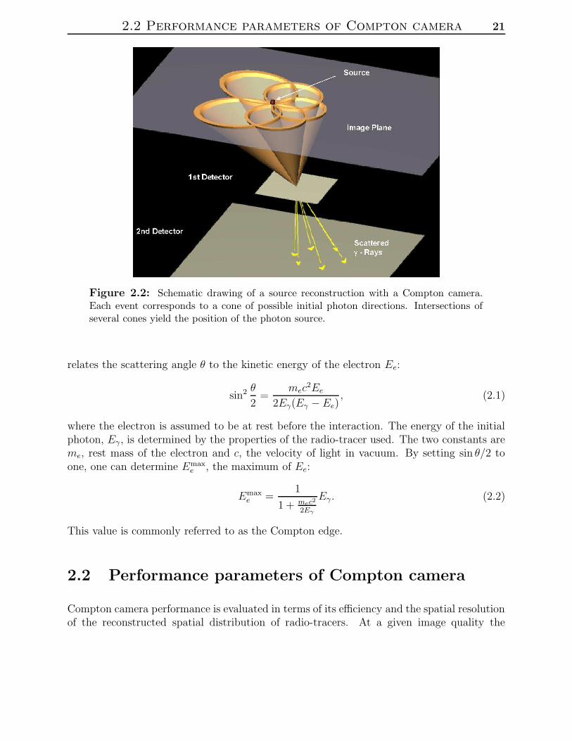
With the scattering angle determined, all possible directions of the incoming photon forma surface of a cone: the axis of the cone is given by the scattered photon direction, theopening angle equals the scattering angle and the apex is fixed to the interaction point inthe scatterer. Figure 2.2 illustrates the conical ambiguity of each of the reconstructed eventsand how intersection of several events yields the position of the photon source1.
Normally energy resolution of the absorber is much lower than resolution of the scatterer andenergy measured in the absorber is only used for rejection of background events. Namely inthe case of proper matching, the sum of the kinetic energy of the electron and the energy ofthe scattered photon is equal to the energy of the initial photon. However if energy resolutionof the absorber is comparable to energy resolution of the scatterer, a factor
√2 gain in energy
resolution is obtained if energies measured in both sub-detectors are considered.2
The equation relating the scattering angle to the energy transfer is determined from theenergy-momentum conservation laws. The expression, relevant for the Compton camera
1This procedure is sometimes referred to as electronic collimation since collimation is done with a sensorand associated electronics rather than with a mechanical collimator.
2N. H. Clinthorne. US patent #6,323,492; 2001.
2.2 Performance parameters of Compton camera 21
Figure 2.2: Schematic drawing of a source reconstruction with a Compton camera.Each event corresponds to a cone of possible initial photon directions. Intersections ofseveral cones yield the position of the photon source.
relates the scattering angle θ to the kinetic energy of the electron Ee:
sin2 θ
2=
mec2Ee
2Eγ(Eγ − Ee), (2.1)
where the electron is assumed to be at rest before the interaction. The energy of the initialphoton, Eγ , is determined by the properties of the radio-tracer used. The two constants areme, rest mass of the electron and c, the velocity of light in vacuum. By setting sin θ/2 toone, one can determine Emax
e , the maximum of Ee:
Emaxe =
1
1 + mec2
2Eγ
Eγ . (2.2)
This value is commonly referred to as the Compton edge.
2.2 Performance parameters of Compton camera
Compton camera performance is evaluated in terms of its efficiency and the spatial resolutionof the reconstructed spatial distribution of radio-tracers. At a given image quality the

22 2. Basic principles of Compton Camera operation
efficiency of a Compton camera is expected to exceed that of an Anger camera by severalorders of magnitude. With higher efficiency the procedure can be optimized either for lowerradiation doses absorbed by the patient or shorter imaging times, giving a sequence of imagesdepicting the physiology of the selected tissue. The spatial resolution of the reconstructedsource distribution determines the smallest features still visible on the image. SPECT canbe also used for searches of cancer lesions, and the smaller the discovered abnormalities, thebetter the chance for a successful treatment.
The efficiency of the Compton camera is the portion of photons emitted by the radio-tracerwhich is used in the reconstruction of the radio-tracer spatial distribution. For an event tobe reconstructed, the following sequence of events has to occur:
• a photon is emitted in the solid angle covered by the scatterer
• the photon undergoes Compton scattering in the scatterer
• the scattered photon escapes from the scatterer, its direction within the solid anglespanned by the absorber
• the scattered photon is detected in the absorber
The efficiency depends substantially on the radio-nuclide bonded in the radio-tracer, so ashort summary of the radio-nuclides used in contemporary SPECT imagers will follow laterin this Chapter. On top of that, the efficiency depends on the detector geometry, and anevaluation for a specific prototype will be given with the prototype description in Chapter5. Because of the underlying conical ambiguity the efficiency of a Compton camera shouldnot be directly compared to the efficiency of an Anger camera and a more detailed analysisof a comparison procedure will be given in Chapter 7
The limited resolution of the Compton collimation is exhibited as broadening of the coneformed by possible directions of incoming photon. The measure of the broadening is an an-gular probability distribution function (pdf) with the scattering angle as an argument, whichis a cross-section of probability through the thickened cone3. In the following discussion, theangular resolution is determined as the full-width-at-half-maximum (FWHM) of this angularpdf. Spatial resolution (in terms of FWHM of the spatial distribution) is proportional to thedetermined separation dsrc−scat between the source and the scatterer and evaluated angularresolution.
There are three contributions to the angular resolution: the inherent resolution given byDoppler broadening, the contribution of limited energy resolution of the scatterer and ge-ometric contribution related to determination of the scattered photon track. The formertwo contributions depend significantly on the selected radio-nuclide so they will be discussedfollowing the introduction of the radio-tracers suitable for SPECT imaging with Compton
3In an ideal case of perfect resolution, the pdf is a δ() function.
2.3 Radio-tracers for SPECT imaging with a Compton camera23
camera, given in the next section. The geometric contribution however depends substantiallyon the detector layout and will be evaluated for actual prototype in Chapter 5.
2.3 Radio-tracers for SPECT imaging with a Compton
camera
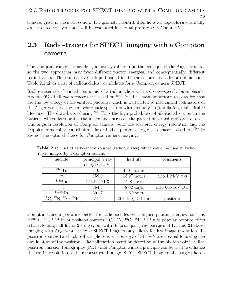
The Compton camera principle significantly differs from the principle of the Anger camera,so the two approaches may favor different photon energies, and consequentially, differentradio-tracers. The radio-active isotope bonded in the radio-tracer is called a radionuclide.Table 2.1 gives a list of radionuclides , candidates for a Compton camera SPECT.
Radio-tracer is a chemical compound of a radionuclide with a disease-specific bio-molecule.About 90% of all radio-tracers are based on 99mTc. The most important reasons for thatare the low energy of the emitted photons, which is well-suited to mechanical collimators ofthe Anger cameras, the monochromatic spectrum with virtually no β-radiation, and suitablelife-time. The draw-back of using 99mTc is the high probability of additional scatter in thepatient, which deteriorates the image and increases the patient-absorbed radio-active dose.The angular resolution of Compton camera, both the scatterer energy resolution and theDoppler broadening contribution, favor higher photon energies, so tracers based on 99mTcare not the optimal choice for Compton camera imaging.
Table 2.1: List of radio-active sources (radionuclides) which could be used in radio-tracers imaged by a Compton camera.
nuclide principal γ-ray half-life commentsenergies [keV]
99mTc 140.5 6.01 hours123I 159.0 13.27 hours also 1 MeV β-s
111mIn 245.5, 171.3 2.8 days131I 364.5 8.02 days also 606 keV β-s
113m1In 391.7 1.6 hours11C, 13N, 15O, 18F 511 20.4, 9.9, 2, 1 min positron
Compton camera performs better for radionuclides with higher photon energies, such as111mIn, 131I, 113m1In or positron sources 11C, 13N, 15O, 18F. 111mIn is popular because of itsrelatively long half life of 2.8 days, but with its principal γ-ray energies of 171 and 245 keV,imaging with Anger-camera type SPECT imagers only allows for low image resolution. Inpositron sources two back-to-back photons with energy of 511 keV are created following theannihilation of the positron. The collimation based on detection of the photon pair is calledpositron emission tomography (PET) and Compton camera principle can be used to enhancethe spatial resolution of the reconstructed image [S. 01]. SPECT imaging of a single photon
24 2. Basic principles of Compton Camera operation
of the pair is also interesting since it doesn’t require the second photon to be detected. Thepositron sources are isotopes of elements frequent in human tissue and there are virtually nolimitations on the bio-molecule selection, and the high energy of the photons decreases theprobability of photon scatter in the tissue. Due to the collimator penetrability, an Angercamera is not practical at such photon energies and a Compton camera may well prove itsadvantage.
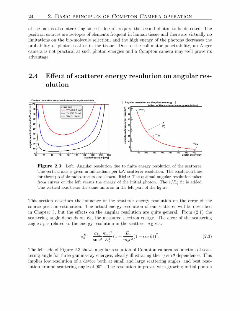
2.4 Effect of scatterer energy resolution on angular res-
olution
scattering angle [deg]0 20 40 60 80 100 120 140 160 180
angu
lar
reso
lutio
n [m
rad/
keV
sca
t.res
.]
0
10
20
30
40
50
60
70
80
90
100
Effects of the scatterer energy resolution on the angular resolution
-rays fromγTc (140.5 keV)99m
In (245.5 keV)111
Na (511 keV)22
photon energy [keV]150 200 250 300 350 400 450 500
optim
al a
ngul
ar r
esol
utio
n [m
rad/
keV
]
5
10
15
20
25
30
35
40
Angular resolution vs. the photon energy
2γE
1
Tc99m
In111
Na22
(effect of the scatterer’s energy resolution)
Figure 2.3: Left: Angular resolution due to finite energy resolution of the scatterer.The vertical axis is given in miliradians per keV scatterer resolution. The resolution linesfor three possible radio-tracers are shown. Right: The optimal angular resolution takenfrom curves on the left versus the energy of the initial photon. The 1/E2
γ fit is added.The vertical axis bears the same units as in the left part of the figure.
This section describes the influence of the scatterer energy resolution on the error of thesource position estimation. The actual energy resolution of our scatterer will be describedin Chapter 3, but the effects on the angular resolution are quite general. From (2.1) thescattering angle depends on Ee, the measured electron energy. The error of the scatteringangle σθ is related to the energy resolution in the scatterer σE via:
σEθ =
σEe
sin θ
mec2
E2γ
(
1 +Eγ
mec2(1 − cos θ)
)2. (2.3)
The left side of Figure 2.3 shows angular resolution of Compton camera as function of scat-tering angle for three gamma-ray energies, clearly illustrating the 1/ sin θ dependence. Thisimplies low resolution of a device both at small and large scattering angles, and best reso-lution around scattering angle of 90 . The resolution improves with growing initial photon
2.5 Doppler broadening 25
energy. The right side of Figure 2.3 illustrates this improvement, showing the best resolutionobtainable for a given initial photon energy. The improvement scales approximately with1/E2
γ , as depicted on the image.
2.5 Doppler broadening
Doppler broadening represents an inherent limit on the Compton camera angular resolution.In this thesis we will present the mechanism of the broadening and its effect on the eventreconstruction. Equation (2.1) assumes the bound electron to be at rest before the interac-tion, while in fact it is moving randomly within the atom or the crystal. Due to symmetry ofCompton scattering the only important quantity is pz, the component of ~p, the electron mo-mentum, parallel to ~q, the scattering momentum, which is defined as the difference between~k′, the scattered photon momentum and ~k, the initial photon momentum:
~q = ~k′ − ~k. (2.4)
Recalculating the Compton relation (2.1) yields the following equations:
sin2 θ
2=
mc2Ee
2Eγ(Eγ − Ee)− ∆~p, (2.5)
∆~p =pzc qc
2Eγ(Eγ − Ee), (2.6)
qc =√
E2γ − 2(Eγ − Ee) cos θ + (Eγ − Ee)2 (2.7)
The term ∆~p is the correction to (2.1) and qc is the magnitude of the scattering momentum.
The above relations imply that a given pair (Ee, θ) determines a value pz:
pz(Ee, θ) =1
qc
(
Eemc2 − (Eγ − Ee)Eγ(1 − cos θ)
)
(2.8)
The probability that for a given energy transfer Ee the scattering angle equals θ is given withJ(pz), the probability that pz(Ee, θ) will be encountered in the interaction. Values J(pz) arealso called Compton profiles and they presented a great interest to atomic physicists sincethey offer a glimpse into the movement of the electron in an atom. Each atomic shell exhibitsa different Compton profile and for an accurate evaluation of the effect, correct weighting hasto be applied based on the probability that an electron from a certain shell is encountered.The tabulated values of J(pz) in [WP72] already account for that.
Our aim is to determine the scattering cross-section d2σdEedθ
, which is proportional to theprobability that the photon will transfer Ee while scattering for θ. Since the encountered
26 2. Basic principles of Compton Camera operation
momentum component is independent from the energy transfer, we can write:
d2σ
dEedpz=
dσ
dEeJ(pz). (2.9)
where dσdEe
is the conventional, unbroadened Klein-Nishina differential cross-section. Chang-
ing the variables to Ee and θ gives d2σ/dEedθ = d2σ/dEedpz |dpz/dθ|. Inserting the deriva-tive of (2.8) gives the double differential Klein-Nishina cross-section (DDKNXS):
d2σ
dEedθ= πr2
0
mc2(Eγ − Ee)
Eγ(qc)2
(
1 + cos2 θ +E2
e
Eγ(Eγ − Ee)
)(
pzc + qc
)
J(pz) (2.10)
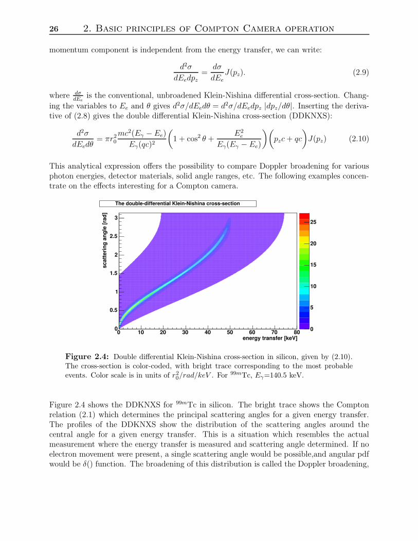
This analytical expression offers the possibility to compare Doppler broadening for variousphoton energies, detector materials, solid angle ranges, etc. The following examples concen-trate on the effects interesting for a Compton camera.
energy transfer [keV]0 10 20 30 40 50 60 70 80
scat
teri
ng a
ngle
[rad
]
0
0.5
1
1.5
2
2.5
3
0
5
10
15
20
25
The double-differential Klein-Nishina cross-section
Figure 2.4: Double differential Klein-Nishina cross-section in silicon, given by (2.10).The cross-section is color-coded, with bright trace corresponding to the most probableevents. Color scale is in units of r2
0/rad/keV . For 99mTc, Eγ=140.5 keV.
Figure 2.4 shows the DDKNXS for 99mTc in silicon. The bright trace shows the Comptonrelation (2.1) which determines the principal scattering angles for a given energy transfer.The profiles of the DDKNXS show the distribution of the scattering angles around thecentral angle for a given energy transfer. This is a situation which resembles the actualmeasurement where the energy transfer is measured and scattering angle determined. If noelectron movement were present, a single scattering angle would be possible,and angular pdfwould be δ() function. The broadening of this distribution is called the Doppler broadening,
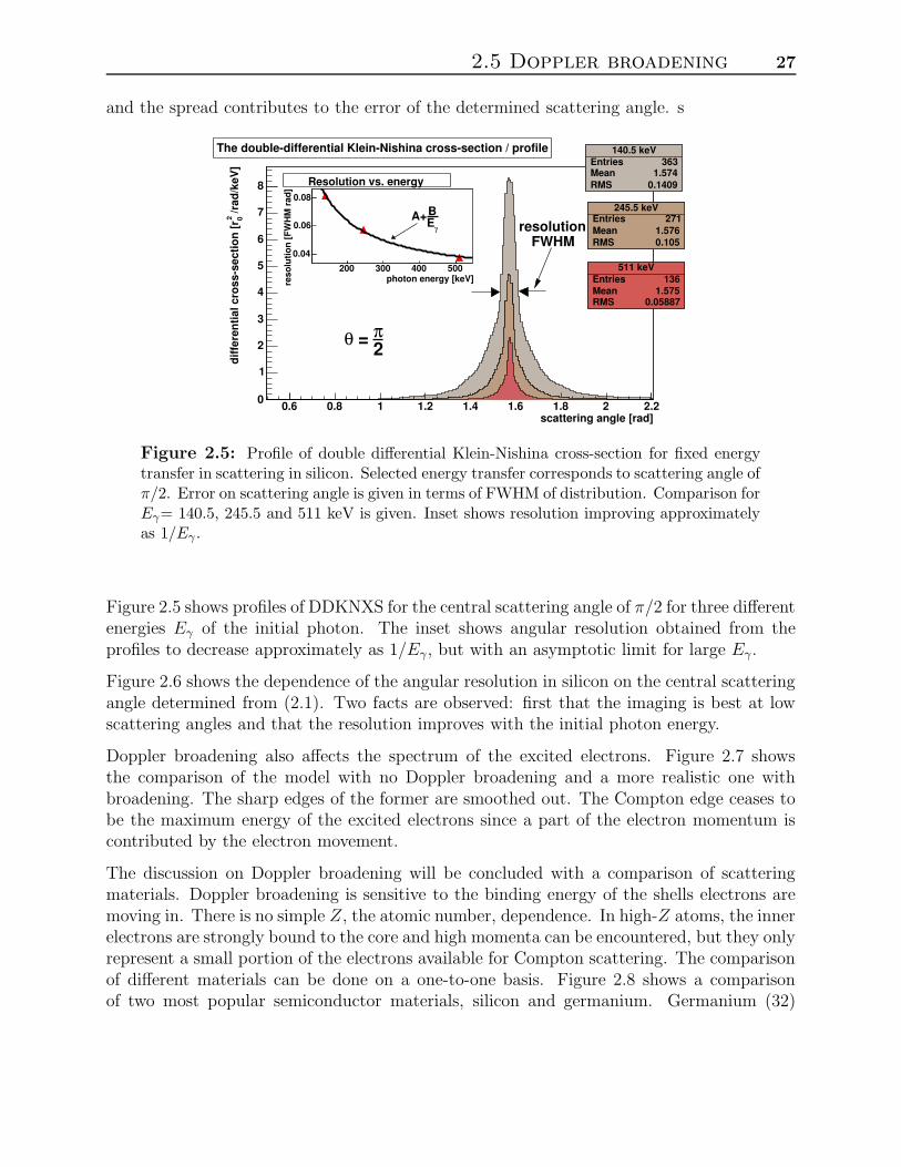
2.5 Doppler broadening 27
and the spread contributes to the error of the determined scattering angle. s
140.5 keVEntries 363Mean 1.574RMS 0.1409
scattering angle [rad]0.6 0.8 1 1.2 1.4 1.6 1.8 2 2.2
/rad
/keV
]2 0
diff
eren
tial c
ross
-sec
tion
[r
0
1
2
3
4
5
6
7
8
140.5 keVEntries 363Mean 1.574RMS 0.1409
The double-differential Klein-Nishina cross-section / profile
245.5 keVEntries 271Mean 1.576RMS 0.105
245.5 keVEntries 271Mean 1.576RMS 0.105
245.5 keVEntries 271Mean 1.576RMS 0.105
511 keVEntries 136Mean 1.575RMS 0.05887
511 keVEntries 136Mean 1.575RMS 0.05887
photon energy [keV]200 300 400 500
reso
lutio
n [F
WH
M r
ad]
0.04
0.06
0.08
Resolution vs. energy
γEBA+
2π = θ
FWHMresolution
Figure 2.5: Profile of double differential Klein-Nishina cross-section for fixed energytransfer in scattering in silicon. Selected energy transfer corresponds to scattering angle ofπ/2. Error on scattering angle is given in terms of FWHM of distribution. Comparison forEγ= 140.5, 245.5 and 511 keV is given. Inset shows resolution improving approximatelyas 1/Eγ .
Figure 2.5 shows profiles of DDKNXS for the central scattering angle of π/2 for three differentenergies Eγ of the initial photon. The inset shows angular resolution obtained from theprofiles to decrease approximately as 1/Eγ, but with an asymptotic limit for large Eγ.
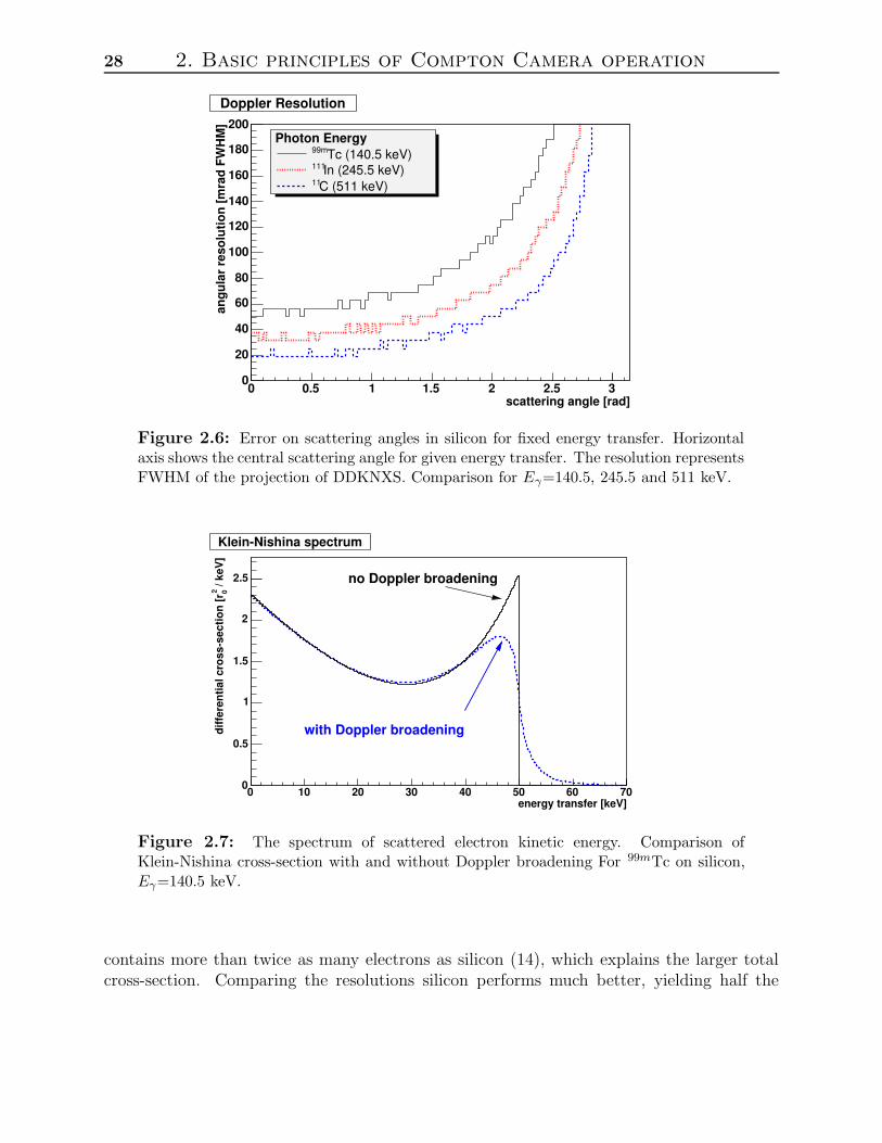
Figure 2.6 shows the dependence of the angular resolution in silicon on the central scatteringangle determined from (2.1). Two facts are observed: first that the imaging is best at lowscattering angles and that the resolution improves with the initial photon energy.
Doppler broadening also affects the spectrum of the excited electrons. Figure 2.7 showsthe comparison of the model with no Doppler broadening and a more realistic one withbroadening. The sharp edges of the former are smoothed out. The Compton edge ceases tobe the maximum energy of the excited electrons since a part of the electron momentum iscontributed by the electron movement.
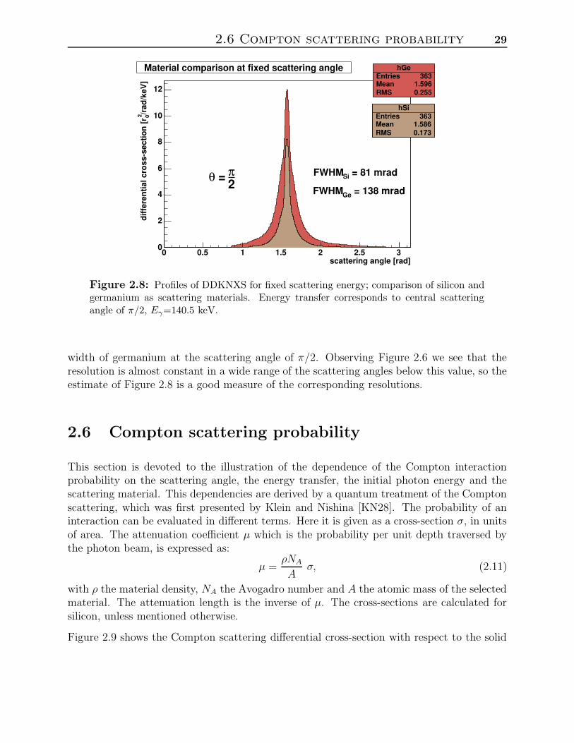
The discussion on Doppler broadening will be concluded with a comparison of scatteringmaterials. Doppler broadening is sensitive to the binding energy of the shells electrons aremoving in. There is no simple Z, the atomic number, dependence. In high-Z atoms, the innerelectrons are strongly bound to the core and high momenta can be encountered, but they onlyrepresent a small portion of the electrons available for Compton scattering. The comparisonof different materials can be done on a one-to-one basis. Figure 2.8 shows a comparisonof two most popular semiconductor materials, silicon and germanium. Germanium (32)
28 2. Basic principles of Compton Camera operation
scattering angle [rad]0 0.5 1 1.5 2 2.5 3
angu
lar
reso
lutio
n [m
rad
FWH
M]
0
20
40
60
80
100
120
140
160
180
200
Doppler Resolution
Photon EnergyTc (140.5 keV)99m
In (245.5 keV)111
C (511 keV)11
Figure 2.6: Error on scattering angles in silicon for fixed energy transfer. Horizontalaxis shows the central scattering angle for given energy transfer. The resolution representsFWHM of the projection of DDKNXS. Comparison for Eγ=140.5, 245.5 and 511 keV.
energy transfer [keV]0 10 20 30 40 50 60 70
/ ke
V]
2 0di
ffer
entia
l cro
ss-s
ectio
n [r
0
0.5
1
1.5
2
2.5
Klein-Nishina spectrum
no Doppler broadening
with Doppler broadening
Figure 2.7: The spectrum of scattered electron kinetic energy. Comparison ofKlein-Nishina cross-section with and without Doppler broadening For 99mTc on silicon,Eγ=140.5 keV.
contains more than twice as many electrons as silicon (14), which explains the larger totalcross-section. Comparing the resolutions silicon performs much better, yielding half the
2.6 Compton scattering probability 29
hGeEntries 363Mean 1.596RMS 0.255
scattering angle [rad]0 0.5 1 1.5 2 2.5 3
/rad
/keV
]2 0
diff
eren
tial c
ross
-sec
tion
[r
0
2
4
6
8
10
12
hGeEntries 363Mean 1.596RMS 0.255
Material comparison at fixed scattering angle
hSiEntries 363Mean 1.586RMS 0.173
hSiEntries 363Mean 1.586RMS 0.173
hSiEntries 363Mean 1.586RMS 0.173
= 81 mradSiFWHM
= 138 mradGeFWHM2π = θ
Figure 2.8: Profiles of DDKNXS for fixed scattering energy; comparison of silicon andgermanium as scattering materials. Energy transfer corresponds to central scatteringangle of π/2, Eγ=140.5 keV.
width of germanium at the scattering angle of π/2. Observing Figure 2.6 we see that theresolution is almost constant in a wide range of the scattering angles below this value, so theestimate of Figure 2.8 is a good measure of the corresponding resolutions.
2.6 Compton scattering probability
This section is devoted to the illustration of the dependence of the Compton interactionprobability on the scattering angle, the energy transfer, the initial photon energy and thescattering material. This dependencies are derived by a quantum treatment of the Comptonscattering, which was first presented by Klein and Nishina [KN28]. The probability of aninteraction can be evaluated in different terms. Here it is given as a cross-section σ, in unitsof area. The attenuation coefficient µ which is the probability per unit depth traversed bythe photon beam, is expressed as:
µ =ρNA
Aσ, (2.11)
with ρ the material density, NA the Avogadro number and A the atomic mass of the selectedmaterial. The attenuation length is the inverse of µ. The cross-sections are calculated forsilicon, unless mentioned otherwise.
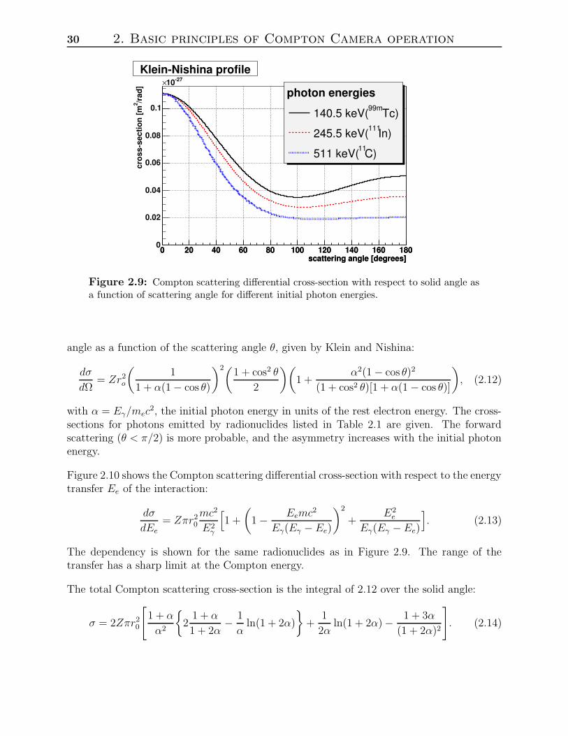
Figure 2.9 shows the Compton scattering differential cross-section with respect to the solid
30 2. Basic principles of Compton Camera operation
scattering angle [degrees]0 20 40 60 80 100 120 140 160 180
scattering angle [degrees]0 20 40 60 80 100 120 140 160 180
/rad
]2
cros
s-se
ctio
n [m
0
0.02
0.04
0.06
0.08
0.1
-2710×Klein-Nishina profile
photon energies
Tc)99m140.5 keV(
In)111245.5 keV(
C)11511 keV(
Figure 2.9: Compton scattering differential cross-section with respect to solid angle asa function of scattering angle for different initial photon energies.
angle as a function of the scattering angle θ, given by Klein and Nishina:
dσ
dΩ= Zr2
o
(
1
1 + α(1 − cos θ)
)2(1 + cos2 θ
2
)(
1 +α2(1 − cos θ)2
(1 + cos2 θ)[1 + α(1 − cos θ)]
)
, (2.12)
with α = Eγ/mec2, the initial photon energy in units of the rest electron energy. The cross-
sections for photons emitted by radionuclides listed in Table 2.1 are given. The forwardscattering (θ < π/2) is more probable, and the asymmetry increases with the initial photonenergy.
Figure 2.10 shows the Compton scattering differential cross-section with respect to the energytransfer Ee of the interaction:
dσ
dEe= Zπr2
0
mc2
E2γ
[
1 +
(
1 − Eemc2
Eγ(Eγ − Ee)
)2
+E2
e
Eγ(Eγ − Ee)
]
. (2.13)
The dependency is shown for the same radionuclides as in Figure 2.9. The range of thetransfer has a sharp limit at the Compton energy.
The total Compton scattering cross-section is the integral of 2.12 over the solid angle:
σ = 2Zπr20
[
1 + α
α2
21 + α
1 + 2α− 1
αln(1 + 2α)
+1
2αln(1 + 2α) − 1 + 3α
(1 + 2α)2
]
. (2.14)
2.6 Compton scattering probability 31
energy transfer [keV]0 50 100 150 200 250 300 350
energy transfer [keV]0 50 100 150 200 250 300 350
cros
s-se
ctio
n [m
^2/k
eV]
0
2
4
6
8
10
12
14
16
18
20-3010×
Klein-Nishina profile
photon energies
Tc)99m140.5 keV(
In)111245.5 keV(
C)11511 keV(
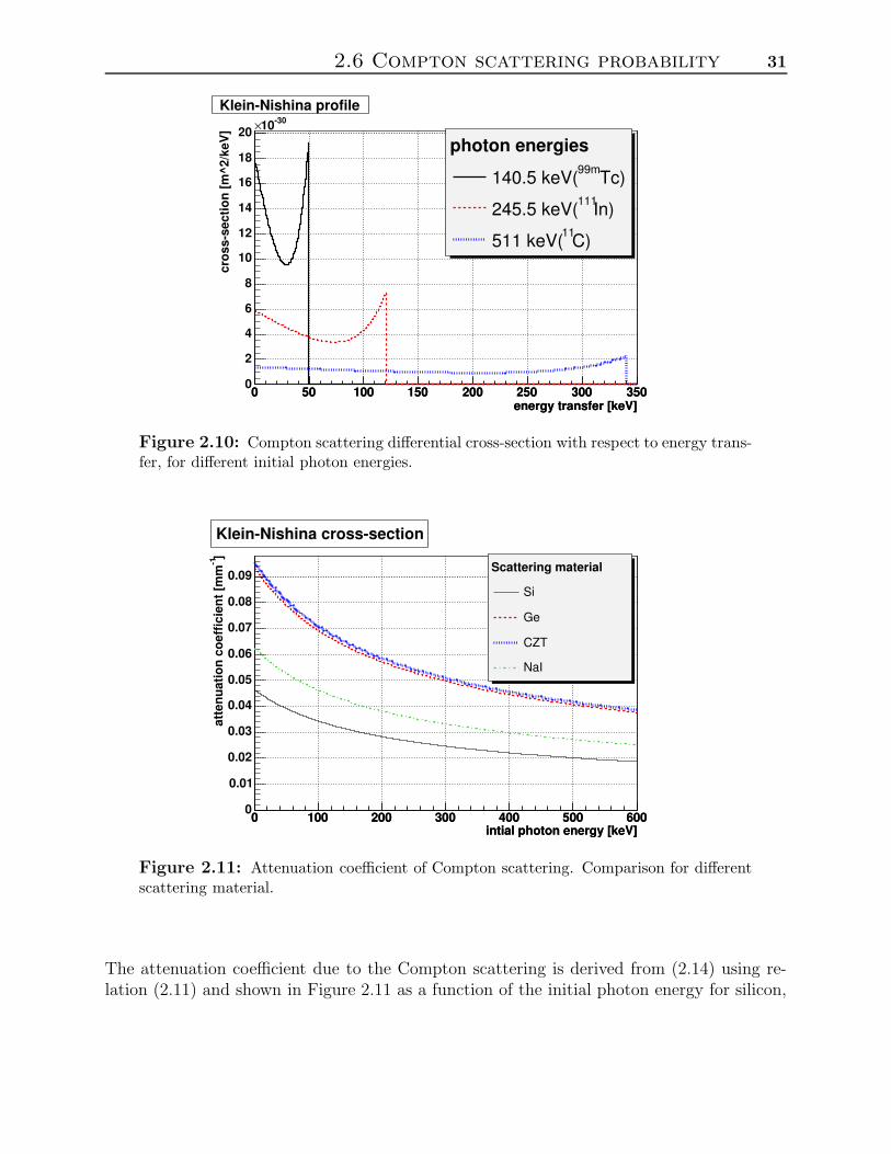
Figure 2.10: Compton scattering differential cross-section with respect to energy trans-fer, for different initial photon energies.
intial photon energy [keV]0 100 200 300 400 500 600
intial photon energy [keV]0 100 200 300 400 500 600
]-1
atte
nuat
ion
coef
ficie
nt [m
m
0
0.01
0.02
0.03
0.04
0.05
0.06
0.07
0.08
0.09
Klein-Nishina cross-section
Scattering material
Si
Ge
CZT
NaI
Figure 2.11: Attenuation coefficient of Compton scattering. Comparison for differentscattering material.
The attenuation coefficient due to the Compton scattering is derived from (2.14) using re-lation (2.11) and shown in Figure 2.11 as a function of the initial photon energy for silicon,
32 2. Basic principles of Compton Camera operation
germanium, CZT and NaI. The probability of Compton scattering decreases with growingphoton energy, a factor of 2 incurred between 60 and 600 keV.
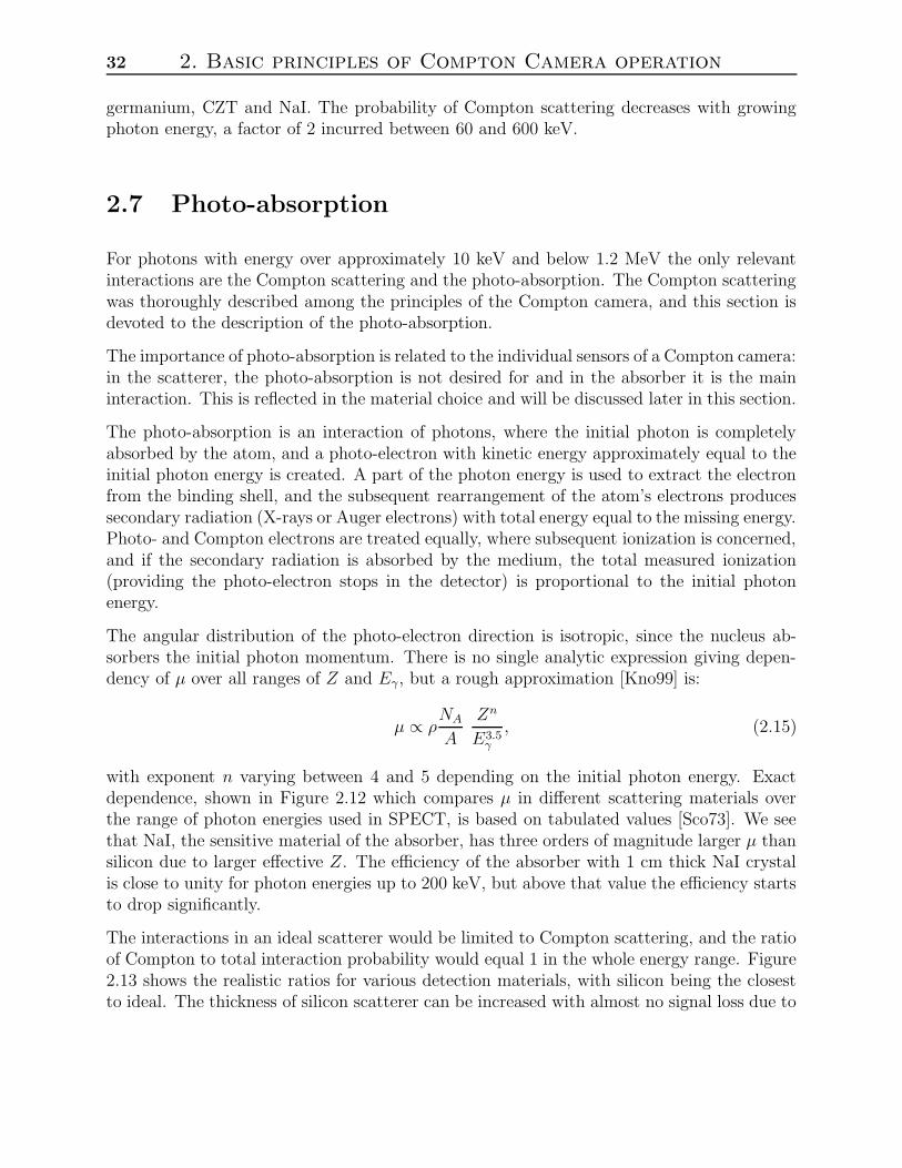
2.7 Photo-absorption
For photons with energy over approximately 10 keV and below 1.2 MeV the only relevantinteractions are the Compton scattering and the photo-absorption. The Compton scatteringwas thoroughly described among the principles of the Compton camera, and this section isdevoted to the description of the photo-absorption.
The importance of photo-absorption is related to the individual sensors of a Compton camera:in the scatterer, the photo-absorption is not desired for and in the absorber it is the maininteraction. This is reflected in the material choice and will be discussed later in this section.
The photo-absorption is an interaction of photons, where the initial photon is completelyabsorbed by the atom, and a photo-electron with kinetic energy approximately equal to theinitial photon energy is created. A part of the photon energy is used to extract the electronfrom the binding shell, and the subsequent rearrangement of the atom’s electrons producessecondary radiation (X-rays or Auger electrons) with total energy equal to the missing energy.Photo- and Compton electrons are treated equally, where subsequent ionization is concerned,and if the secondary radiation is absorbed by the medium, the total measured ionization(providing the photo-electron stops in the detector) is proportional to the initial photonenergy.
The angular distribution of the photo-electron direction is isotropic, since the nucleus ab-sorbers the initial photon momentum. There is no single analytic expression giving depen-dency of µ over all ranges of Z and Eγ, but a rough approximation [Kno99] is:
µ ∝ ρNA
A
Zn
E3.5γ
, (2.15)
with exponent n varying between 4 and 5 depending on the initial photon energy. Exactdependence, shown in Figure 2.12 which compares µ in different scattering materials overthe range of photon energies used in SPECT, is based on tabulated values [Sco73]. We seethat NaI, the sensitive material of the absorber, has three orders of magnitude larger µ thansilicon due to larger effective Z. The efficiency of the absorber with 1 cm thick NaI crystalis close to unity for photon energies up to 200 keV, but above that value the efficiency startsto drop significantly.
The interactions in an ideal scatterer would be limited to Compton scattering, and the ratioof Compton to total interaction probability would equal 1 in the whole energy range. Figure2.13 shows the realistic ratios for various detection materials, with silicon being the closestto ideal. The thickness of silicon scatterer can be increased with almost no signal loss due to
2.7 Photo-absorption 33
photon energy [MeV]-310 -210 -110 1
photon energy [MeV]-310 -210 -110 1
]-1
atte
nuat
ion
coef
ficie
nt [m
m
-510
-410
-310
-210
-110
1
10
210
310
Photo-absorption probability
Scattering materialSi
NaI
Ge
CZT
Figure 2.12: Photo-absorption attenuation coefficient as function of initial photonenergy for various detector media. Data from [Sco73]. Both X and Y scale are logarithmic!
initial photon energy [keV]0 100 200 300 400 500 600
initial photon energy [keV]0 100 200 300 400 500 600
port
ion
of C
ompt
on in
tera
ctio
ns
0
0.2
0.4
0.6
0.8
1
Compton to total attenuation ratio
Scattering material
Si
Ge
CZT
NaI
Figure 2.13: Compton to total attenuation ratio in various media, data from [Sco73,HVB+75].
the photo-absorption, giving a great enhancement of the scatterer’s efficiency, which is notthe case for the rest of the listed detection material.

34 2. Basic principles of Compton Camera operation

Chapter 3
Scatterer
As already described, the scatterer is the first sensor of a Compton camera in which thescattering of the initial photon takes place. The scatterer with the associated electronics hasto provide several pieces of information: the location of the interaction, the measurementof the energy transfer and a trigger signal for timing correlation with the absorber. Theserequirements present complex technical challenges, causing previous Compton camera pro-totypes to fall somewhat short of their design goals. Because of that, we devoted specialattention to development of the scatterer.
Recent years have seen substantial progress in the field of silicon sensors. Practically everymajor high energy physics experiment constructed in the last decade includes a set of positionsensitive silicon detectors at its core. The potential for medical imaging applications, whereX-ray and γ-rays are imaged, was also quickly recognized and silicon is by many claimed tobe the best semiconductor detection material available. The following reasons favor it as theCompton camera scatterer material:
• suitable energy resolution at the room temperature,
• high resistivity substrates, giving manageable depletion voltages for 1 mm thick sensors,
• robustness,
• Doppler broadening is lower than in any other semiconductor material,
• high ratio of Compton to photo absorption interaction cross-section,
• manageable cost,
• excellent spatial resolution on the impact position.
The only draw-back of silicon as a γ-ray sensor is its low attenuation coefficient. The thick-ness of a sensor is limited by the production process and manageable depletion voltages, butstacking of sensors can increase efficiency, hence reducing the problem.
35
36 3. Scatterer
This chapter describes the development and performance of a Compton camera scatterer.First the properties of silicon pad sensors are given and the signal formation and operationconditions described. We continue with the description of electronic processing of the signal,with special attention given to the first stage of readout electronics embedded in an appli-cation specific integrated circuit (ASIC). Performance of the assembly in terms of energyresolution and timing properties is described and evaluated in terms of requirements of theCompton camera scatterer.
3.1 Basics of silicon pad sensor operation
Silicon is a semiconductor material and the common property of all semiconductors is a gapin the electron energy band structure around the Fermi level. This makes them insulatorsat low temperature and conductors with moderate resistivity at room temperature. Theenergy gap in silicon is 1.12 keV, and the resistivity of a pure (intrinsic) silicon sample atroom temperature would be 300 kΩcm.
Years ago it was demonstrated that a semiconductor can be used as a particle detector,exhibiting high efficiency and energy and spatial resolutions. The invention became widelyused and semiconductors are presently one of the most popular detector materials.
Al
p+
n
n+
Al
VT
scattered photon
initial photon
electronexcited
+
__ _ _
+++
E
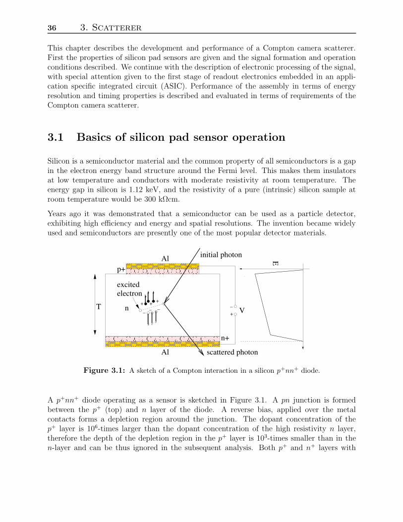
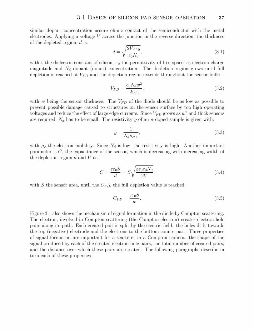
Figure 3.1: A sketch of a Compton interaction in a silicon p+nn+ diode.
A p+nn+ diode operating as a sensor is sketched in Figure 3.1. A pn junction is formedbetween the p+ (top) and n layer of the diode. A reverse bias, applied over the metalcontacts forms a depletion region around the junction. The dopant concentration of thep+ layer is 106-times larger than the dopant concentration of the high resistivity n layer,therefore the depth of the depletion region in the p+ layer is 103-times smaller than in then-layer and can be thus ignored in the subsequent analysis. Both p+ and n+ layers with
3.1 Basics of silicon pad sensor operation 37
similar dopant concentration assure ohmic contact of the semiconductor with the metalelectrodes. Applying a voltage V across the junction in the reverse direction, the thicknessof the depleted region, d is:
d =
√
2V εε0
e0Nd
, (3.1)
with ε the dielectric constant of silicon, ε0 the permittivity of free space, e0 electron chargemagnitude and Nd dopant (donor) concentration. The depletion region grows until fulldepletion is reached at VFD and the depletion region extends throughout the sensor bulk:
VFD =e0Ndw
2
2εε0
, (3.2)
with w being the sensor thickness. The VFD of the diode should be as low as possible toprevent possible damage caused to structures on the sensor surface by too high operatingvoltages and reduce the effect of large edge currents. Since VFD grows as w2 and thick sensorsare required, Nd has to be small. The resistivity % of an n-doped sample is given with:
% =1
Ndµee0, (3.3)
with µe the electron mobility. Since Nd is low, the resistivity is high. Another importantparameter is C, the capacitance of the sensor, which is decreasing with increasing width ofthe depletion region d and V as:
C =εε0S
d= S
√
εε0e0Nd
2V, (3.4)
with S the sensor area, until the CFD, the full depletion value is reached:
CFD =εε0S
w. (3.5)
Figure 3.1 also shows the mechanism of signal formation in the diode by Compton scattering.The electron, involved in Compton scattering (the Compton electron) creates electron-holepairs along its path. Each created pair is split by the electric field: the holes drift towardsthe top (negative) electrode and the electrons to the bottom counterpart. Three propertiesof signal formation are important for a scatterer in a Compton camera: the shape of thesignal produced by each of the created electron-hole pairs, the total number of created pairs,and the distance over which these pairs are created. The following paragraphs describe inturn each of these properties.
38 3. Scatterer
The number of electron-hole pairs produced by the Compton electron is proportional to itskinetic energy or the energy transfer of the interaction. The number of created electron-holepairs is subject to fluctuations, since the energy is distributed among the created electron-hole pairs and phonon excitations. Ne−h, the average number of created pairs is given by:
Ne−h =Ee
η, (3.6)
with ηSi=3.6 keV, the average energy required to create an electron-hole pair in silicon. Q,the total charge collected on the readout electrode is then:
Q = Ne−he0 =e0Ee
η. (3.7)
For Compton edges of the radionuclides listed in Table 2.1, there are 13800, 33400 and 94600electron-hole pairs created for 99mTc, 111In and 11C, respectively.
Fano[Fan47] calculated the fluctuation of Ne−h:
σF =√
FNe−h, (3.8)
with FSi=0.1, the Fano factor named after him. The fluctuation σF is much smaller thancorresponding carrier number fluctuation of an ionization chamber and semiconductors haveexcellent intrinsic energy resolution. The error σF is given as a number of electrons, whichleads to the convention that all errors on energy measurement in semiconductors are ex-pressed in this units. The intrinsic error on Ne−h is given as 37, 57 and 97 e at Comptonedges of 99mTc, 111In and 11C, respectively.
The Compton electron is causing ionization in the semiconductor until its energy falls belowη, then it is swept to the electrode by the electric field. The total distance between theinteraction point and the most distant secondary ionization point is called the electronrange, and it plays an important role in the reconstruction of the interaction position. Sincesecondary ionization is a random process, the electron path is not a straight line, but a windypath with many abrupt turns and it is impossible to locate either the interaction point orthe end of the track. The total signal is thus treated as a cloud of electron-hole pairs,with the position of the scattering as its center of weight. The inherent spatial resolutionof a semiconductor when locating a photon interaction point is therefore the range of theCompton electron1.
1The only exception to the rule occurs for electrons with ranges exceeding the volume of the sensor cell.If the length of the path is long enough and the energy of the electron high enough, the interaction end ofthe signal is calculated using Bethe-Bloch formula for differential energy loss as a function of electron energy.For medical imaging the initial photon energy is much too small, so the stated rule is valid.
3.1 Basics of silicon pad sensor operation 39
electron energy [keV]10 210
electron energy [keV]10 210
rang
e [m
m]
-310
-210
-110
1
Electron Range in Silicon
Figure 3.2: Range of electrons in silicon as a function of their kinetic energy. Data aretaken from [UM84].
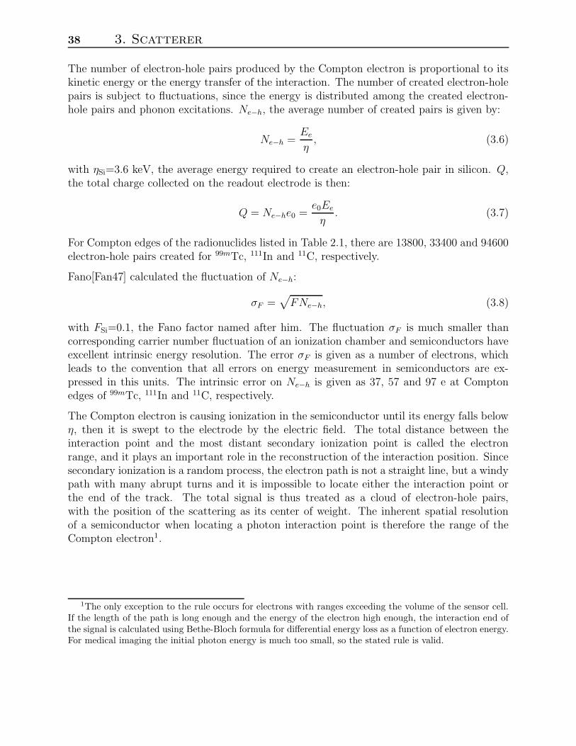
Figure 3.2 shows the range of electron in silicon as a function of its kinetic energy. TheCompton electron range is 24, 110 and 550 µm for electrons with the Compton edge energyof 99mTc, 111In and 11C radionuclide, respectively.
Table 3.1 lists the important detection parameters of silicon as scatterer for radionuclideslisted in Table 2.1. The maximum kinetic energy (the Compton edge) of Compton electronswas used to characterize the individual radionuclides.
Table 3.1: Silicon detection properties of the Compton electrons with maximum energy(the Compton edge) of the listed radionuclides.
Radionuclide Photon Compton Number of created Error on Ne−h, Electronenergy [keV] edge [keV] e-h pairs Ne−h σF range [mm]
99mTc 140.5 49.8 13847 37 0.024111In 245.5 120.3 33417 57 0.1111C 511 340.7 94630 97 0.55
In semiconductor detectors the signal presented to the electronics is the current induced onthe electrodes by the moving carriers. The number of carriers is small enough that they canbe treated separately and independently. According to the Ramo theorem[Ram39] a movingcharge in an electric field induces a current pulse on the readout electrode with the currentpulse shape i(t) given by
i(t) = q~v(t) ~Ew, (3.9)
where q is the charge of the carrier, ~v its velocity and ~Ew the weighting potential. The
40 3. Scatterer
velocity of the carrier is related to ~E the electric field:
~vi = µi~E, (3.10)
with µi the carrier mobility and index i marking the carrier type (e-lectrons,h-oles). Theelectric field as a function of x, measured from the p+n junction is given by:
E(x) = −V
w− e0Nd
εε0
(
w
2− x
)
, (3.11)
where V > VFD is the applied reverse bias. The field is pointing towards, the coordinatesystem away from the p+n junction, which makes the electric field (3.11) negative, as shownin Figure 3.1. It is convenient for a pad sensor fabrication to make the p+ electrode thereadout electrode so the current pulse shapes of each carrier type on that electrode will becalculated. The weighting field in a diode is constant and parallel to the electric field:
Ew = −1/w. (3.12)
In a pad sensor the weighting field partially stretches towards the adjacent electrodes andequation (3.12) can be only treated as an approximation and used for an illustration of theproduced pulse shapes.
0 20 40 60 80 100
sign
al [A
]
0
2
4
6
8-1210× Signal
=0.1 w0x
eh
0 20 40 60 80 100
sign
al [A
]
0
2
4
6
8-1210× Signal
=0.5 w0xe h
time [ns]0 20 40 60 80 100
sign
al [A
]
0
2
4
6
8-1210× Signal
=0.9 w0x
he
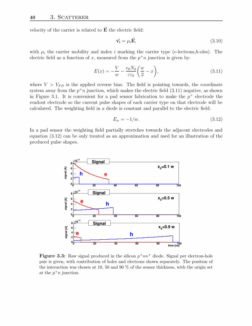
Figure 3.3: Raw signal produced in the silicon p+nn+ diode. Signal per electron-holepair is given, with contribution of holes and electrons shown separately. The position ofthe interaction was chosen at 10, 50 and 90 % of the sensor thickness, with the origin setat the p+n junction.
3.1 Basics of silicon pad sensor operation 41
The equation of carrier motion (3.10) is solved to yield vi(t), which is combined with (3.12)and the Ramo pulse shape to yield the respective pulse shapes:
ie = Ae0
τee−
tτe , (3.13)
ih = Ae0
τh
et
τh , (3.14)
with τi = εε0/µie0Nd, and A, dimensionless constant. A depends on x0, the depth ofinteraction and V , the applied bias:
A =1
2
(
V
VFD
+ 1
)
− x0
w. (3.15)
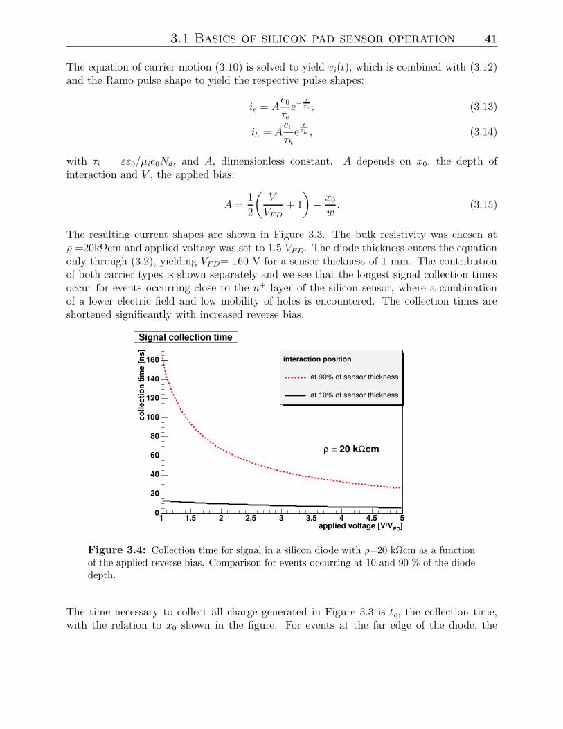
The resulting current shapes are shown in Figure 3.3. The bulk resistivity was chosen at% =20kΩcm and applied voltage was set to 1.5 VFD. The diode thickness enters the equationonly through (3.2), yielding VFD= 160 V for a sensor thickness of 1 mm. The contributionof both carrier types is shown separately and we see that the longest signal collection timesoccur for events occurring close to the n+ layer of the silicon sensor, where a combinationof a lower electric field and low mobility of holes is encountered. The collection times areshortened significantly with increased reverse bias.
]FDapplied voltage [V/V1 1.5 2 2.5 3 3.5 4 4.5 5
colle
ctio
n tim
e [n
s]
0
20
40
60
80
100
120
140
160
Signal collection time
interaction position
at 90% of sensor thickness
at 10% of sensor thickness
cmΩ = 20 kρ
Figure 3.4: Collection time for signal in a silicon diode with %=20 kΩcm as a functionof the applied reverse bias. Comparison for events occurring at 10 and 90 % of the diodedepth.
The time necessary to collect all charge generated in Figure 3.3 is tc, the collection time,with the relation to x0 shown in the figure. For events at the far edge of the diode, the
42 3. Scatterer
hole contribution is dominant and thc , the collection time of the created holes is the relevantparameter. The situation is reversed at the near edge, with te
c, the collection time of the
electrons. Both are derived from the integral∫ EDGE
x0dx/v and the velocity given by (3.10).
The corresponding collection times are:
thc = τh ln
(
1 + VVFD
1 + VVFD
− 2x0
w
)
, (3.16)
tec = τe ln
(
3 + VVFD
1 + VVFD
+ 2x0
w
)
. (3.17)
The combined collection time as a function of the depletion voltage is shown in Figure 3.4.Comparison for events occurring at near edge (10% of the diode depth) and the far edge (90%of the depth) is given. Over-biasing greatly improves the performance, with the collectiontime shortening for a factor of 2.5 when the voltage is varied from VFD to 2VFD, for eventsoccurring at the far edge.
3.2 Front-end electronics
The task of the front-end electronics is:
• to provide an analog signal proportional to the energy of the Compton electron
• to generate a timing trigger.
This is reflected in the circuit organization. The signal part generates the analog signal andthe trigger part generates the trigger. The properties of each of the parts will be thoroughlydiscussed in the following subsections.
Further stages of electronics are more important in terms of data organization and communi-cation. The second stage generates the operation parameters of the first stage, and collectsand organizes the data. The next stage does the analog to digital conversion, packs thedata into an event and communicates the data to the storage and control device, the PC.The computer is the last stage of the processing, managing task such as controlling the dataflow, storing the data and performing off-line data analysis. Their importance on the datacollection is not as crucial as the performance of the front-end, and they will be presentedbriefly later on.
To obtain position sensitivity, a segmentation of the sensor is required and this is reflected inparallelization of the front-end electronics into independent channels. The following discus-sion is limited to a single processing channel, but the actual circuit has to supply as manychannels as there are pads in the diode array.
3.2 Front-end electronics 43
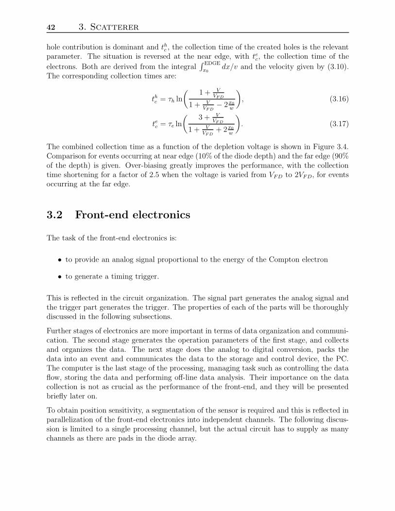
3.2.1 Signal part
The signal part of the front-end electronics has to provide an analog signal proportional tothe energy of the Compton electron. The measured energy is then used for the scatteringangle determination, via the Compton camera principle. Thus the measurement error willbe reflected in the reconstructed source resolution. To maximize the resolution, a low-noiseprocessing circuit is required.
C
R
C
R
R
C
R
vout
Rp
p
u u
preamplifier differentiator integrator
CD is
SENSOR
s
s s
s
SHAPER
to SAMPLE & HOLD
Figure 3.5: A schematic representation of the signal part of each channel of the front-end electronics circuit together with the sensor.
Figure 3.5 shows a schematic of the signal part circuit. The input is the diode signal currentis(t) and the output the voltage vout(t). The processing chain is composed of a charge-sensitive pre-amplifier and a CR-RC shaper.
The raw signal (Figure 3.3) is first integrated on a charge-sensitive pre-amplifier with acapacitive feed-back Cp. The input capacitance seen by the signal is ApCp, with Ap theamplification factor of the pre-amplifier, which exceeds the sensor capacitance Cd, and thecharge is integrated over Cp. If no resistor is present in the feed-back, the output of thepre-amplifier is a constant voltage Q/Cp, proportional to the energy of the excited electron,cf. (3.7). A feed-back resistor Rp, is added to restore the base-line in τp = RpCp, thepre-amplifier relaxation time. For an impulse, Qδ(t0), the voltage at the output of thepre-amplifier is given by:
vp(t) =Q
Cpe−
t−t0τp , (3.18)
for t > t0.
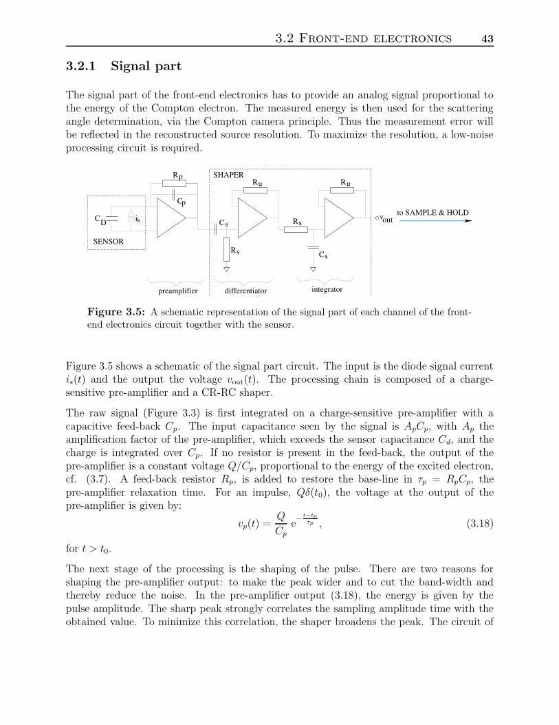
The next stage of the processing is the shaping of the pulse. There are two reasons forshaping the pre-amplifier output: to make the peak wider and to cut the band-width andthereby reduce the noise. In the pre-amplifier output (3.18), the energy is given by thepulse amplitude. The sharp peak strongly correlates the sampling amplitude time with theobtained value. To minimize this correlation, the shaper broadens the peak. The circuit of
44 3. Scatterer
3.5 shows a shaper made of a single differentiation stage (C-R) and a single integration stage(R-C) with equal characteristic time τE
s = RsCs. The response of the circuit to an impulse(δ(t)) is shown in Figure 3.6. The output of the pre-amplifier (equation (3.18)) is shown forcomparison. The blow-up on the inset shows the rounded-off peak appearing at fixed timeτEs after the physical event. The negative peak of the shaper is called the undershoot and it
is an artifact due to the zero-restoration part of the pre-amplifier. Indeed, the shaped pulseand the output of the pre-amplifier restore a zero voltage with the same relaxation time τp.Ignoring this, the shaped response to an impulse input is given with:
vout(t) =Q
Cp
(t − t0)
τse−
t−t0τEs . (3.19)
The amplitude of the generated signal is proportional to the Compton electron energy andis given by:
vsignal =Q
Cpe, (3.20)
where e is the base of ln. The amplitude is extracted from the pulse by a SAMPLE & HOLDcircuit which will be described later in this chapter.
s]µtime [0 10 20 30 40 50
s]µtime [0 10 20 30 40 50
] pCQ
volta
ge [
0
0.2
0.4
0.6
0.8
1
The circuit impulse response
output ofpreamplifiershaper
epCQ
sµ=3 sτ
sµ=20 pτ
s]µtime [0 5 10
s]µtime [0 5 10
] pCQ
volta
ge [
0
0.2
Shaper response
Figure 3.6: Impulse response of a pre-amplifier with characteristic time τp = 20µsand a shaper with τE
s = 3µs. The impulse integral equals Q, the pre-amplifier feed-backcapacitance Cp. The characteristic times resemble those of the actual prototype.
The signal is super-imposed on the fluctuating base-line. The error on the sampled amplitudeis therefore equal to base-line variation, which is also called the noise of the signal. Thesignal is a voltage pulse, and the noise Vn is most naturally expressed in volts, but since we
3.2 Front-end electronics 45
are interested in the collected charge Q and related energy Ee, it will be expressed as anequivalent noise charge (ENC) σn or energy resolution ∆E. The relation to Vn is extractedusing relations (3.20) and (3.7):
σn = VnCpe, (3.21)
∆E = (2.35 × η)σn = 8.5 × VnCpe. (3.22)
The energy resolution ∆E is expressed as FWHM and the ENC as the variance of thedistribution of the base-line fluctuations, and the factor 2
√
2 ln(2) = 2.35 converts thevariance to FWHM, and the combined value of 8.5 includes the silicon specific ηSi=3.6.The following discussion will derive the variance of the fluctuation based on spectral powerdensities of noise sources appearing in processing chain.
vout
C
Rp
p
CD is in
SENSOR
ia
eaSHAPER
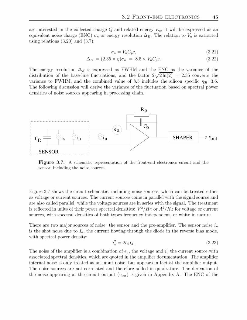
Figure 3.7: A schematic representation of the front-end electronics circuit and thesensor, including the noise sources.
Figure 3.7 shows the circuit schematic, including noise sources, which can be treated eitheras voltage or current sources. The current sources come in parallel with the signal source andare also called parallel, while the voltage sources are in series with the signal. The treatmentis reflected in units of their power spectral densities: V 2/Hz or A2/Hz for voltage or currentsources, with spectral densities of both types frequency independent, or white in nature.
There are two major sources of noise: the sensor and the pre-amplifier. The sensor noise in
is the shot noise due to Id, the current flowing through the diode in the reverse bias mode,with spectral power density:
i2n = 2e0Id. (3.23)
The noise of the amplifier is a combination of ea, the voltage and ia the current source withassociated spectral densities, which are quoted in the amplifier documentation. The amplifierinternal noise is only treated as an input noise, but appears in fact at the amplifier output.The noise sources are not correlated and therefore added in quadrature. The derivation ofthe noise appearing at the circuit output (vout) is given in Appendix A. The ENC of the
46 3. Scatterer
output is determined to be:
σn =
√
e2
8
(
e2aC
21
τs+ (2e0Id + i2a) τs
)
, (3.24)
with C = Cd + Cp + Cr + Cin the total capacitance seen by the pre-amplifier, including Cin,the amplifier input capacitance and Cr, the stray capacitance which includes the capacitanceof the lines connecting the sensor output and the pre-amplifier. In order to reduce Cr theproximity of electronics and sensor is of vital importance. Equation 3.24 has an optimizationparameter, τs, which can be selected to minimize σn. The shape of (3.24) ensures theexistence of a minimum:
τEs =
eaC√
2e0Id + i2a, (3.25)
which depends on the diode current and the parameters of the amplifier.
3.2.2 Trigger part
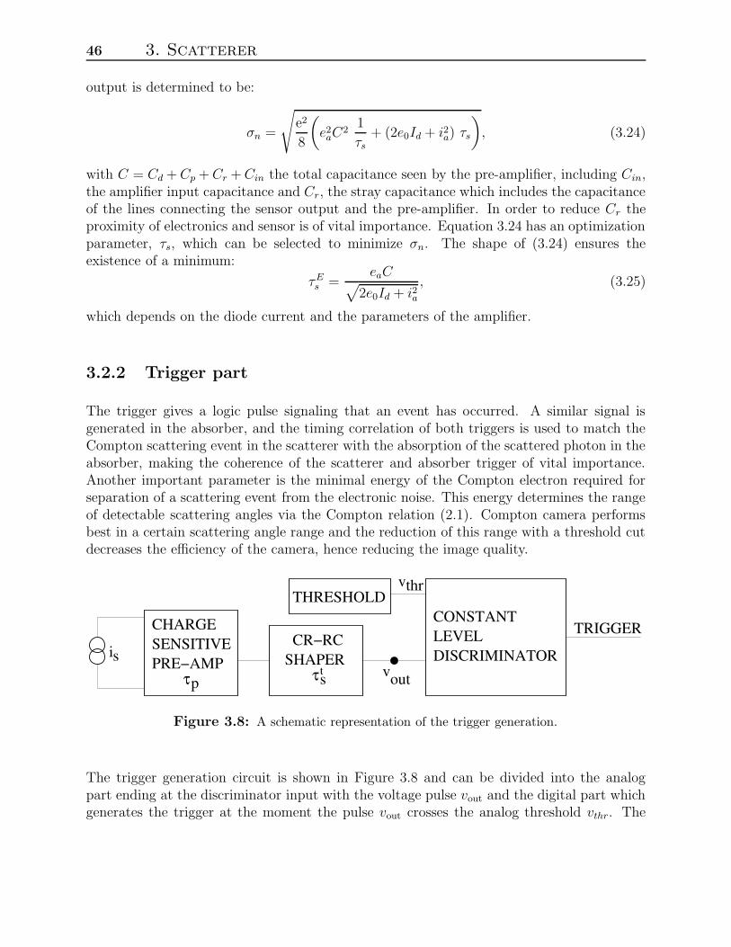
The trigger gives a logic pulse signaling that an event has occurred. A similar signal isgenerated in the absorber, and the timing correlation of both triggers is used to match theCompton scattering event in the scatterer with the absorption of the scattered photon in theabsorber, making the coherence of the scatterer and absorber trigger of vital importance.Another important parameter is the minimal energy of the Compton electron required forseparation of a scattering event from the electronic noise. This energy determines the rangeof detectable scattering angles via the Compton relation (2.1). Compton camera performsbest in a certain scattering angle range and the reduction of this range with a threshold cutdecreases the efficiency of the camera, hence reducing the image quality.
SHAPERτs vout
CR−RCCHARGESENSITIVEPRE−AMP
τp
THRESHOLD
DISCRIMINATORLEVELCONSTANT
TRIGGER
vthr
ist
Figure 3.8: A schematic representation of the trigger generation.
The trigger generation circuit is shown in Figure 3.8 and can be divided into the analogpart ending at the discriminator input with the voltage pulse vout and the digital part whichgenerates the trigger at the moment the pulse vout crosses the analog threshold vthr. The
3.2 Front-end electronics 47
important parameters of the trigger are the timing resolution and the minimal detectableenergy for a given noise rate.
Minimal detectable energy. The derivation of the minimal detectable energy of theinteraction electron is given in two parts: first the minimal detectable charge is calculatedand then the corresponding energy. The minimal detectable charge is related to the ENCof the analog trigger part. The parameters of the analog output vout are described by theequations derived for the analog signal (3.24,3.20), since the architectures of the triggeranalog part and the analog signal are identical (shown in Figure 3.5). Furthermore, sincethe trigger shaping time τ t
s is much shorter than the shaping time τEs , which minimizes (3.24),
the noise in the trigger pulse is dominated by voltage noise of the pre-amplifier and currentnoise can be ignored. Hence, the noise (ENC) of the trigger analog pulse is approximatedby:
σtn =
e
2√
2eaC
1√
τ ts
, (3.26)
and the minimal charge giving an analog pulse exceeding the threshold voltage is given byQmin = vthrCpe using equation (3.20). The distribution of base-line fluctuation amplitudesis Gaussian, and the rate of excursions exceeding voltage vthr (or charge Qmin) is given with[Ric45]:
fn =1
4√
3τ ts
e−
Q2min
2(σtn)2 , (3.27)
Selecting a rate of noise triggers fr which can be tolerated in an operating setup sets Qmin,by inversion of (3.27):
Qmin = σtn
√
−2 log(
4√
3τsfr
)
. (3.28)
Expressing the rate of noise triggers as:
fr = 10−αr/τ ts, (3.29)
the minimal detectable charge for a fixed σtn is given by:
Qmin =√
4.6αr − 3.9σt. (3.30)
For example, αr = 6 gives Qmin=5σtn. The minimal detectable energy can be further com-
promised by a charge loss due to τ ts shorter than the charge collection time tc. The effect is
characterized by a factor B representing charge collection efficiency, with B ≤1. Since chargecollection time tc (equations (3.17) and (3.16)) depends on the position of the interaction,the same is valid for charge collection efficiency. The charge collected on the electrode isQc = BQ = BEee0/η, and the minimum detectable energy Ee,min of the interaction electronis:
Ee,min =η
B e0Qmin. (3.31)
48 3. Scatterer
Timing resolution. Two sources contribute to timing resolution of the trigger signal: thejitter and the time-walk. The source of the jitter is the base-line fluctuation: the analogvoltage vout(t) is the sum of the signal and the fluctuation and the voltage vthr may beexceeded sooner or later than the time designated by the signal alone. For small fluctuations,the distribution of the trigger time will be Gaussian, centered at the trigger time of the baresignal and the width σjitter given by:
σjitter =V t
ndvout
dt
, (3.32)
with dvout/dt the slope of the voltage pulse at the time of the trigger, and the V tn the noise of
the analog trigger pulse. The slope is estimated using the impulse response (3.19), evaluatedfor t < τ t
s as vout(t) = tτ ts
QCpe
, with the derivative:
dvout
dt=
1
τ ts
Q
Cpe. (3.33)
Converting V tn to (ENC) σt
n (3.21) and inserting expression (3.33) back into (3.32), thevariance of the jitter is obtained:
σjitter =σt
n
Qτ ts, (3.34)
proportional to τ ts for a fixed ENC σt
n and Q, the signal charge. For example - setting thecharge Q=2Qmin, which sets the threshold at Q/2, the slope of the pulse at the threshold iswell approximated with (3.33) giving a jitter of approximately σjitter = τ t
s/10.
The time-walk originates in dependence of the trigger time on the energy of the detectedCompton electron. Since the energy information is not available when the events of thescatterer and the absorber are matched, this dependence should be minimized for a properevent matching. The time-walk is illustrated on the inset of Figure 3.9, showing the triggertiming difference of a signal pair: one with the minimal detectable charge Qmin and anotherwith 5-times larger amplitude. This is a good approximation of the situation encountered ina Compton electron detection: the electron energy spectrum is a continuum and all possiblecharges between Qmin and the maximum detectable charge Qmax,(the Compton edge) aredetected, and the ratio r = Qmax/Qmin is fixed for a given threshold. The large curve showsthe time difference of such signal pairs as a function of r, in units of the shaping time. Withr of 5 and more encountered in a real system, the time-walk is well approximated with theshaping time τ t
s .
The jitter and the time-walk are both proportional to τ ts, and minimized for τ t
s → 0. Theproportionality is valid until τ t
s is decreased to values comparable with the charge collectiontime tc. Below that limit the charge collection efficiency B drops, which also decreases thesignal rise time and the derivative dV/dt. To assess the effects of finite tc, the sensor responseis(t) was modeled by a square function of duration tc.
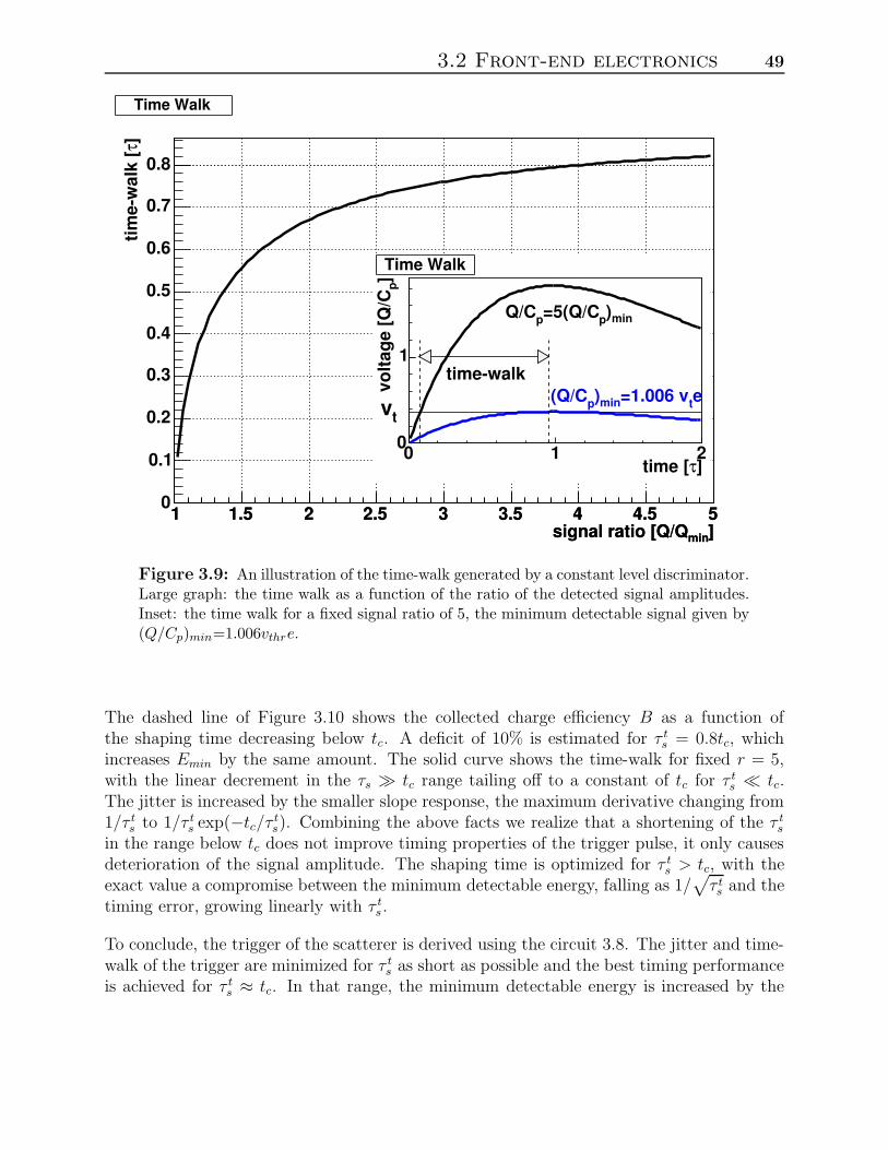
3.2 Front-end electronics 49
]minsignal ratio [Q/Q1 1.5 2 2.5 3 3.5 4 4.5 5
]minsignal ratio [Q/Q1 1.5 2 2.5 3 3.5 4 4.5 5
]τtim
e-w
alk
[
0
0.1
0.2
0.3
0.4
0.5
0.6
0.7
0.8
Time Walk
]τtime [0 1 2
] pvo
ltage
[Q/C
0
1
Time Walk
tv
min)p=5(Q/CpQ/C
et=1.006 vmin)p(Q/Ctime-walk
Figure 3.9: An illustration of the time-walk generated by a constant level discriminator.Large graph: the time walk as a function of the ratio of the detected signal amplitudes.Inset: the time walk for a fixed signal ratio of 5, the minimum detectable signal given by(Q/Cp)min=1.006vthre.
The dashed line of Figure 3.10 shows the collected charge efficiency B as a function ofthe shaping time decreasing below tc. A deficit of 10% is estimated for τ t
s = 0.8tc, whichincreases Emin by the same amount. The solid curve shows the time-walk for fixed r = 5,with the linear decrement in the τs tc range tailing off to a constant of tc for τ t
s tc.The jitter is increased by the smaller slope response, the maximum derivative changing from1/τ t
s to 1/τ ts exp(−tc/τ
ts). Combining the above facts we realize that a shortening of the τ t
s
in the range below tc does not improve timing properties of the trigger pulse, it only causesdeterioration of the signal amplitude. The shaping time is optimized for τ t
s > tc, with theexact value a compromise between the minimum detectable energy, falling as 1/
√
τ ts and the
timing error, growing linearly with τ ts.
To conclude, the trigger of the scatterer is derived using the circuit 3.8. The jitter and time-walk of the trigger are minimized for τ t
s as short as possible and the best timing performanceis achieved for τ t
s ≈ tc. In that range, the minimum detectable energy is increased by the
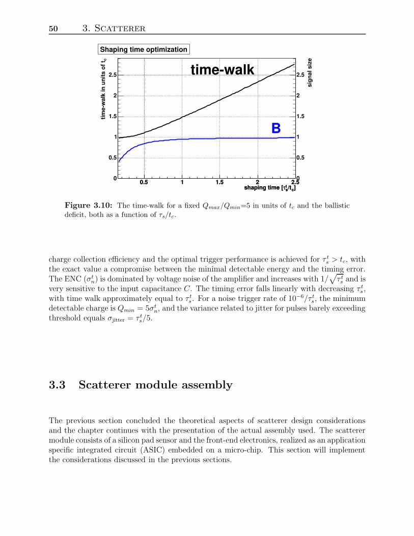
50 3. Scatterer
]c/ttsτshaping time [
0.5 1 1.5 2 2.5]c/tt
sτshaping time [0.5 1 1.5 2 2.5
ctim
e-w
alk
in u
nits
of t
0
0.5
1
1.5
2
2.5
Shaping time optimization
sign
al s
ize
0
0.5
1
1.5
2
2.5
B
time-walk
Figure 3.10: The time-walk for a fixed Qmax/Qmin=5 in units of tc and the ballisticdeficit, both as a function of τs/tc.
charge collection efficiency and the optimal trigger performance is achieved for τ ts > tc, with
the exact value a compromise between the minimal detectable energy and the timing error.The ENC (σt
n) is dominated by voltage noise of the amplifier and increases with 1/√
τ ts and is
very sensitive to the input capacitance C. The timing error falls linearly with decreasing τ ts,
with time walk approximately equal to τ ts. For a noise trigger rate of 10−6/τ t
s, the minimumdetectable charge is Qmin = 5σt
n, and the variance related to jitter for pulses barely exceedingthreshold equals σjitter = τ t
s/5.
3.3 Scatterer module assembly
The previous section concluded the theoretical aspects of scatterer design considerationsand the chapter continues with the presentation of the actual assembly used. The scatterermodule consists of a silicon pad sensor and the front-end electronics, realized as an applicationspecific integrated circuit (ASIC) embedded on a micro-chip. This section will implementthe considerations discussed in the previous sections.
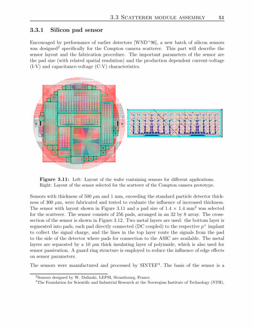
3.3 Scatterer module assembly 51
3.3.1 Silicon pad sensor
Encouraged by performance of earlier detectors [WND+96], a new batch of silicon sensorswas designed2 specifically for the Compton camera scatterer. This part will describe thesensor layout and the fabrication procedure. The important parameters of the sensor arethe pad size (with related spatial resolution) and the production dependent current-voltage(I-V) and capacitance-voltage (C-V) characteristics.
Figure 3.11: Left: Layout of the wafer containing sensors for different applications.Right: Layout of the sensor selected for the scatterer of the Compton camera prototype.
Sensors with thickness of 500 µm and 1 mm, exceeding the standard particle detector thick-ness of 300 µm, were fabricated and tested to evaluate the influence of increased thickness.The sensor with layout shown in Figure 3.11 and a pad size of 1.4 × 1.4 mm2 was selectedfor the scatterer. The sensor consists of 256 pads, arranged in an 32 by 8 array. The cross-section of the sensor is shown in Figure 3.12. Two metal layers are used: the bottom layer issegmented into pads, each pad directly connected (DC coupled) to the respective p+ implantto collect the signal charge, and the lines in the top layer route the signals from the padto the side of the detector where pads for connection to the ASIC are available. The metallayers are separated by a 10 µm thick insulating layer of polyimide, which is also used forsensor passivation. A guard ring structure is employed to reduce the influence of edge effectson sensor parameters.
The sensors were manufactured and processed by SINTEF3. The basis of the sensor is a
2Sensors designed by W. Dulinski, LEPSI, Strassbourg, France.3The Foundation for Scientific and Industrial Research at the Norwegian Institute of Technology (NTH),
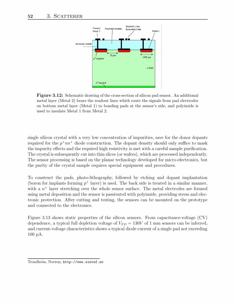
52 3. Scatterer
Figure 3.12: Schematic drawing of the cross-section of silicon pad sensor. An additionalmetal layer (Metal 2) bears the readout lines which route the signals from pad electrodeson bottom metal layer (Metal 1) to bonding pads at the sensor’s side, and polyimide isused to insulate Metal 1 from Metal 2.
single silicon crystal with a very low concentration of impurities, save for the donor dopantsrequired for the p+nn+ diode construction. The dopant density should only suffice to maskthe impurity effects and the required high resistivity is met with a careful sample purification.The crystal is subsequently cut into thin slices (or wafers), which are processed independently.The sensor processing is based on the planar technology developed for micro-electronics, butthe purity of the crystal sample requires special equipment and procedures.
To construct the pads, photo-lithography, followed by etching and dopant implantation(boron for implants forming p+ layer) is used. The back side is treated in a similar manner,with a n+ layer stretching over the whole sensor surface. The metal electrodes are formedusing metal deposition and the sensor is passivated with polyimide, providing stress and elec-tronic protection. After cutting and testing, the sensors can be mounted on the prototypeand connected to the electronics.
Figure 3.13 shows static properties of the silicon sensors. From capacitance-voltage (CV)dependence, a typical full depletion voltage of VFD = 130V of 1 mm sensors can be inferred,and current-voltage characteristics shows a typical diode current of a single pad not exceeding100 pA.
Trondheim, Norway, http://www.sintef.no
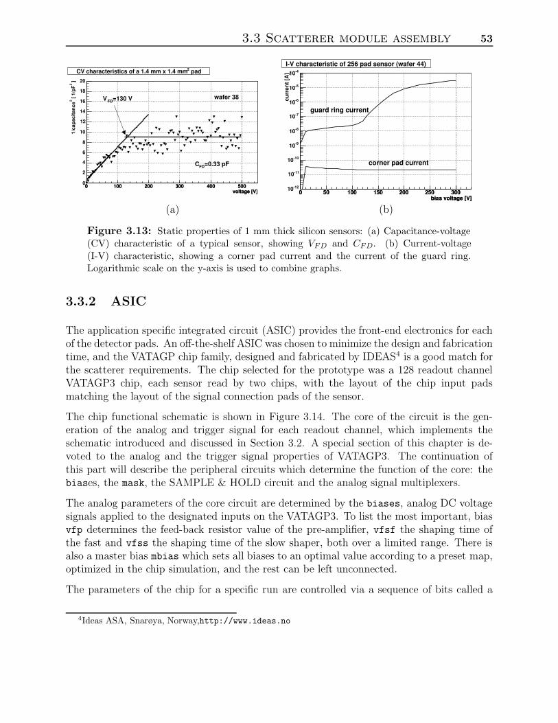
3.3 Scatterer module assembly 53
voltage [V]0 100 200 300 400 500
voltage [V]0 100 200 300 400 500
]2 [
1/pF
21/
capa
cita
nce
0
2
4
6
8
10
12
14
16
18
20
pad2CV characteristics of a 1.4 mm x 1.4 mm
=0.33 pFFDC
=130 VFDV wafer 38
bias voltage [V]0 50 100 150 200 250 300
bias voltage [V]0 50 100 150 200 250 300
curr
ent [
A]
-1210
-1110
-1010
-910
-810
-710
-610
-510
-410
I-V characteristic of 256 pad sensor (wafer 44)
corner pad current
guard ring current
(a) (b)
Figure 3.13: Static properties of 1 mm thick silicon sensors: (a) Capacitance-voltage(CV) characteristic of a typical sensor, showing VFD and CFD. (b) Current-voltage(I-V) characteristic, showing a corner pad current and the current of the guard ring.Logarithmic scale on the y-axis is used to combine graphs.
3.3.2 ASIC
The application specific integrated circuit (ASIC) provides the front-end electronics for eachof the detector pads. An off-the-shelf ASIC was chosen to minimize the design and fabricationtime, and the VATAGP chip family, designed and fabricated by IDEAS4 is a good match forthe scatterer requirements. The chip selected for the prototype was a 128 readout channelVATAGP3 chip, each sensor read by two chips, with the layout of the chip input padsmatching the layout of the signal connection pads of the sensor.
The chip functional schematic is shown in Figure 3.14. The core of the circuit is the gen-eration of the analog and trigger signal for each readout channel, which implements theschematic introduced and discussed in Section 3.2. A special section of this chapter is de-voted to the analog and the trigger signal properties of VATAGP3. The continuation ofthis part will describe the peripheral circuits which determine the function of the core: thebiases, the mask, the SAMPLE & HOLD circuit and the analog signal multiplexers.
The analog parameters of the core circuit are determined by the biases, analog DC voltagesignals applied to the designated inputs on the VATAGP3. To list the most important, biasvfp determines the feed-back resistor value of the pre-amplifier, vfsf the shaping time ofthe fast and vfss the shaping time of the slow shaper, both over a limited range. There isalso a master bias mbias which sets all biases to an optimal value according to a preset map,optimized in the chip simulation, and the rest can be left unconnected.
The parameters of the chip for a specific run are controlled via a sequence of bits called a
4Ideas ASA, Snarøya, Norway,http://www.ideas.no
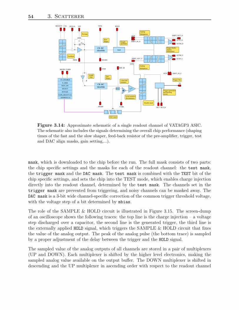
54 3. Scatterer
VTHR
REF_BI
+DAC
discriminatorLevel sensitive
PreAmp
TestMask
3−bit DAC trimmers
ShaperSlow
ShaperFast
OUTP_D
OUTM_D
!!!!!!!!!!""""""""""
###########
$$$$$$$$$$$
%%%%%%%%%%%%&&&&&&&&
''''''''''''((((((((((((
Disable mask
))))))))********
+++++++++
,,,,,,,,--------
............////////////
0000000011111111
222222333333
4444444455555555
6666666677777777
8888888899999999
::::::::;;;;;;;;
<<<<<<<<<<==========>>>>>>>>????????@@@@@@@@@@@@AAAAAAAAAAAA
BBBBBBBBCCCCCCCC DDDDDDDDEEEEEEEE
FFFFFFFFFFFFGGGGGGGGGGGG
PREB
SIGNAL VFPREGOUT CAL
REGIN CLKIN
SHABS
VFSS
VFSF
SHABF
GAIN_SELECT [2]
BYPASS
SELECT
TEST_ON
N_SIDE
CC_ENABLE
ADDRESS [4]
GCK
SHIFT_IN_D
GCK
SHIFT_OUT_U OUTP_U
OUTM_U
GCK SHIFT_IN_U
SHIFT_OUT_D
HOLD
TO
DLT_BDLT
stageGAIN
DAC mask
Trigger Out
Output BufferAnalogDifferential
Trigger generationand blockingcircuit
Analog
Analog
Cfp
SHAPERCR−RC
CR−RCSHAPER
Sampleand Hold
Multiplexer
Multiplexer
S&H
Figure 3.14: Approximate schematic of a single readout channel of VATAGP3 ASIC.The schematic also includes the signals determining the overall chip performance (shapingtimes of the fast and the slow shaper, feed-back resistor of the pre-amplifier, trigger, testand DAC align masks, gain setting,...).
mask, which is downloaded to the chip before the run. The full mask consists of two parts:the chip specific settings and the masks for each of the readout channel: the test mask,the trigger mask and the DAC mask. The test mask is combined with the TEST bit of thechip specific settings, and sets the chip into the TEST mode, which enables charge injectiondirectly into the readout channel, determined by the test mask. The channels set in thetrigger mask are prevented from triggering, and noisy channels can be masked away. TheDAC mask is a 3-bit wide channel-specific correction of the common trigger threshold voltage,with the voltage step of a bit determined by mbias.
The role of the SAMPLE & HOLD circuit is illustrated in Figure 3.15. The screen-dumpof an oscilloscope shows the following traces: the top line is the charge injection – a voltagestep discharged over a capacitor, the second line is the generated trigger, the third line isthe externally applied HOLD signal, which triggers the SAMPLE & HOLD circuit that fixesthe value of the analog output. The peak of the analog pulse (the bottom trace) is sampledby a proper adjustment of the delay between the trigger and the HOLD signal.
The sampled value of the analog outputs of all channels are stored in a pair of multiplexers(UP and DOWN). Each multiplexer is shifted by the higher level electronics, making thesampled analog value available on the output buffer. The DOWN multiplexer is shifted indescending and the UP multiplexer in ascending order with respect to the readout channel
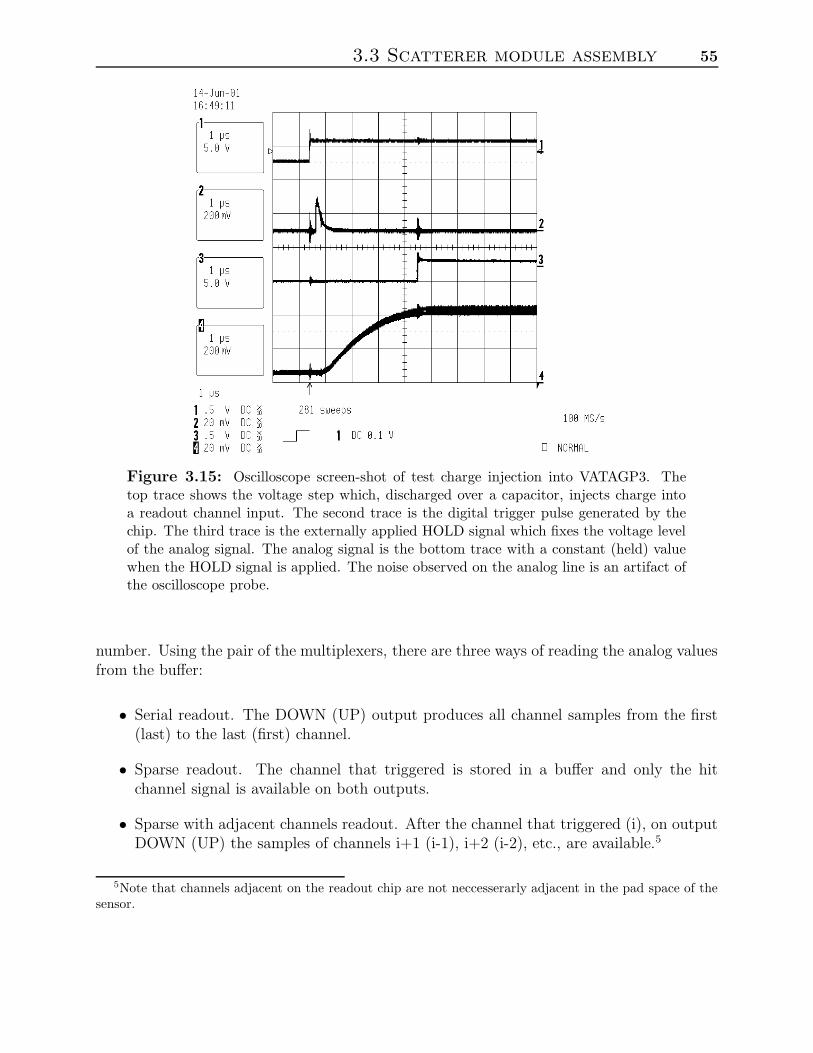
3.3 Scatterer module assembly 55
Figure 3.15: Oscilloscope screen-shot of test charge injection into VATAGP3. Thetop trace shows the voltage step which, discharged over a capacitor, injects charge intoa readout channel input. The second trace is the digital trigger pulse generated by thechip. The third trace is the externally applied HOLD signal which fixes the voltage levelof the analog signal. The analog signal is the bottom trace with a constant (held) valuewhen the HOLD signal is applied. The noise observed on the analog line is an artifact ofthe oscilloscope probe.
number. Using the pair of the multiplexers, there are three ways of reading the analog valuesfrom the buffer:
• Serial readout. The DOWN (UP) output produces all channel samples from the first(last) to the last (first) channel.
• Sparse readout. The channel that triggered is stored in a buffer and only the hitchannel signal is available on both outputs.
• Sparse with adjacent channels readout. After the channel that triggered (i), on outputDOWN (UP) the samples of channels i+1 (i-1), i+2 (i-2), etc., are available.5
5Note that channels adjacent on the readout chip are not neccesserarly adjacent in the pad space of thesensor.
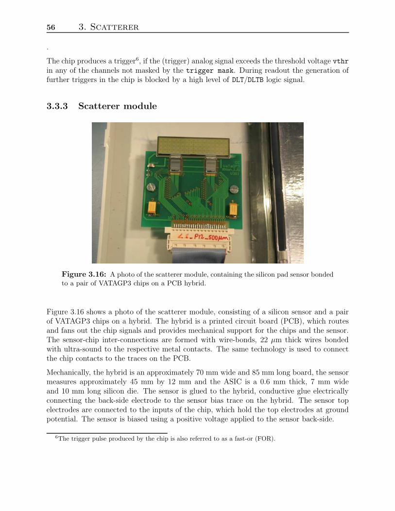
56 3. Scatterer
.
The chip produces a trigger6, if the (trigger) analog signal exceeds the threshold voltage vthrin any of the channels not masked by the trigger mask. During readout the generation offurther triggers in the chip is blocked by a high level of DLT/DLTB logic signal.
3.3.3 Scatterer module
Figure 3.16: A photo of the scatterer module, containing the silicon pad sensor bondedto a pair of VATAGP3 chips on a PCB hybrid.
Figure 3.16 shows a photo of the scatterer module, consisting of a silicon sensor and a pairof VATAGP3 chips on a hybrid. The hybrid is a printed circuit board (PCB), which routesand fans out the chip signals and provides mechanical support for the chips and the sensor.The sensor-chip inter-connections are formed with wire-bonds, 22 µm thick wires bondedwith ultra-sound to the respective metal contacts. The same technology is used to connectthe chip contacts to the traces on the PCB.
Mechanically, the hybrid is an approximately 70 mm wide and 85 mm long board, the sensormeasures approximately 45 mm by 12 mm and the ASIC is a 0.6 mm thick, 7 mm wideand 10 mm long silicon die. The sensor is glued to the hybrid, conductive glue electricallyconnecting the back-side electrode to the sensor bias trace on the hybrid. The sensor topelectrodes are connected to the inputs of the chip, which hold the top electrodes at groundpotential. The sensor is biased using a positive voltage applied to the sensor back-side.
6The trigger pulse produced by the chip is also referred to as a fast-or (FOR).
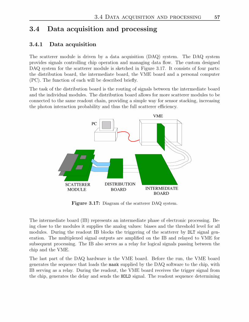
3.4 Data acquisition and processing 57
3.4 Data acquisition and processing
3.4.1 Data acquisition
The scatterer module is driven by a data acquisition (DAQ) system. The DAQ systemprovides signals controlling chip operation and managing data flow. The custom designedDAQ system for the scatterer module is sketched in Figure 3.17. It consists of four parts:the distribution board, the intermediate board, the VME board and a personal computer(PC). The function of each will be described briefly.
The task of the distribution board is the routing of signals between the intermediate boardand the individual modules. The distribution board allows for more scatterer modules to beconnected to the same readout chain, providing a simple way for sensor stacking, increasingthe photon interaction probability and thus the full scatterer efficiency.
VME
PC
DISTRIBUTIONINTERMEDIATE
BOARDBOARD
SCATTERER MODULE
Figure 3.17: Diagram of the scatterer DAQ system.
The intermediate board (IB) represents an intermediate phase of electronic processing. Be-ing close to the modules it supplies the analog values: biases and the threshold level for allmodules. During the readout IB blocks the triggering of the scatterer by DLT signal gen-eration. The multiplexed signal outputs are amplified on the IB and relayed to VME forsubsequent processing. The IB also serves as a relay for logical signals passing between thechip and the VME.
The last part of the DAQ hardware is the VME board. Before the run, the VME boardgenerates the sequence that loads the mask supplied by the DAQ software to the chip, withIB serving as a relay. During the readout, the VME board receives the trigger signal fromthe chip, generates the delay and sends the HOLD signal. The readout sequence determining
58 3. Scatterer
the readout mode is generated and sent to the chip, along with the channel shifting clock(set to 1.2 MHz). The same clock is used by the pair of flash (up to 10 MHz) ADCs whichdigitize both (UP & DOWN) outputs, amplified by the IB. The digitized signals are packedinto an event and stored in the output buffer of the VME controller. Physically, the VMEboard is a PCB, inserted in a VME crate which provides the necessary power supply. TheVME standard (IEEE-1014-1987) is used for communication between the PC and the VMEboard. The software which controls the board’s function is partially executed by the FPGAof the board (readout sequence generation, event packing) but mostly reserved for the PC.
A personal computer (PC) closes the DAQ system loop. PC serves as a master control deviceand storage media. The DAQ software developed and used in the scope of this work collectsand stores the events prepared by the VME board and allows the user to change the maskof the chips and determine the readout mode. A brief on-line analysis program is addedfor quality check of collected data. The complete data analysis is performed off-line on thestored data sets.
3.4.2 Data processing
The aim of processing of the scatterer data is to extract the scatterer-relevant parameters,i.e. to measure the energy and position of the Compton interaction7. This sub-section isdevoted to the description of the software algorithm which determines those parameters.The algorithm will be illustrated on a scatterer calibration run: 241Am γ-rays are detectedby a single scatterer module (Figure 3.16 sensor with 256 pads, 0.5 mm thick, read by 2VATAGP3 chips), and both interaction types (photo-absorption, Compton) are observed.
An event e corresponds to a set of raw ADC digitized values sei for all readout channels, with
channel number (or ID) i. To obtain the base-line or the pedestal pi of channel i, the rawvalues se
i are histogramed. A typical histogram is shown in Figure 3.18. Since either of theNc = 256 channels produces the trigger, the probability that a specific channel i containsa signal charge q is small enough8. Observing Figure 3.18 we can see that a majority ofcollected values is contained in the first peak, exhibiting a Gaussian shape. It correspondsto the sampled fluctuations of the baseline and a Gaussian fit (shown on the inset) is usedto determine the mean, pi and the variance or noise σi of channel i. The sampled valuesabove the peak correspond to the detected signals, with the corresponding detected chargeq = se
i − pi. Subtracting the pedestal pi the signal spectrum is obtained, which correspondsto the spectrum of interaction electrons.
The variance σi obtained from a single channel histogram over-estimates the channel noise,as a part of the base-line fluctuations is caused by power-supply variation of the chip. The
7The scatterer also provides a timing signal, but coincidence timing is done by the front-end electronicsand no additional processing is needed.
8Providing that the source illuminates the whole sensor and the range of the interaction produced electronsis smaller than the pad size.
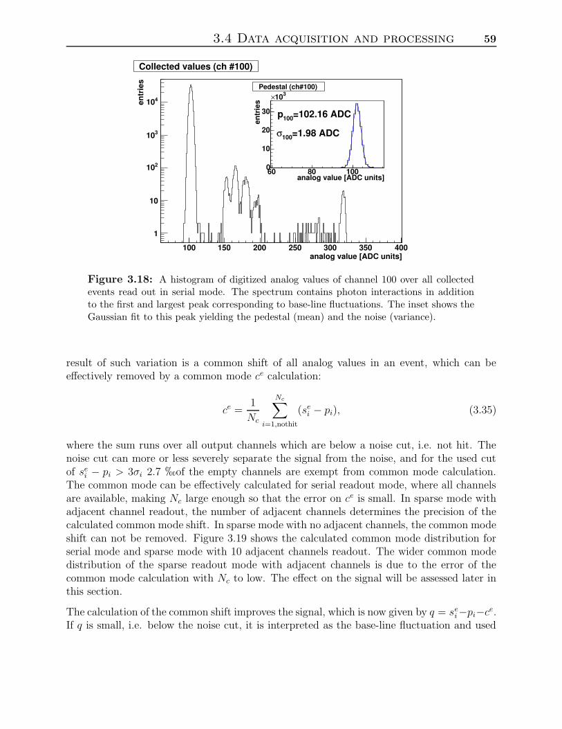
3.4 Data acquisition and processing 59
analog value [ADC units]100 150 200 250 300 350 400
entr
ies
1
10
210
310
410
Collected values (ch #100)
analog value [ADC units]60 80 100
entr
ies
0
10
20
30
310×Pedestal (ch#100)
=1.98 ADC100σ
=102.16 ADC100p
Figure 3.18: A histogram of digitized analog values of channel 100 over all collectedevents read out in serial mode. The spectrum contains photon interactions in additionto the first and largest peak corresponding to base-line fluctuations. The inset shows theGaussian fit to this peak yielding the pedestal (mean) and the noise (variance).
result of such variation is a common shift of all analog values in an event, which can beeffectively removed by a common mode ce calculation:
ce =1
Nc
Nc∑
i=1,nothit
(sei − pi), (3.35)
where the sum runs over all output channels which are below a noise cut, i.e. not hit. Thenoise cut can more or less severely separate the signal from the noise, and for the used cutof se
i − pi > 3σi 2.7 hof the empty channels are exempt from common mode calculation.The common mode can be effectively calculated for serial readout mode, where all channelsare available, making Nc large enough so that the error on ce is small. In sparse mode withadjacent channel readout, the number of adjacent channels determines the precision of thecalculated common mode shift. In sparse mode with no adjacent channels, the common modeshift can not be removed. Figure 3.19 shows the calculated common mode distribution forserial mode and sparse mode with 10 adjacent channels readout. The wider common modedistribution of the sparse readout mode with adjacent channels is due to the error of thecommon mode calculation with Nc to low. The effect on the signal will be assessed later inthis section.
The calculation of the common shift improves the signal, which is now given by q = sei−pi−ce.
If q is small, i.e. below the noise cut, it is interpreted as the base-line fluctuation and used
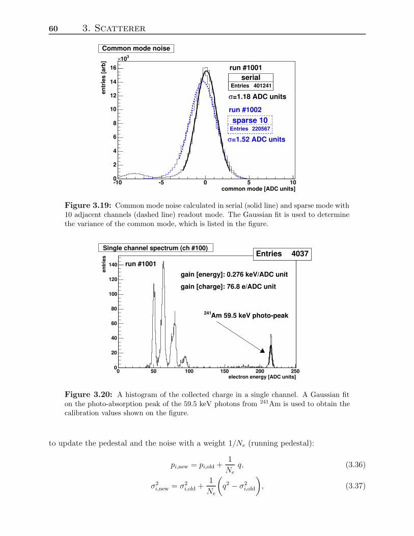
60 3. Scatterer
sparse 10Entries 220567
common mode [ADC units]-10 -5 0 5 10
entr
ies
[arb
]
0
2
4
6
8
10
12
14
16
310×
sparse 10Entries 220567
Common mode noise
serialEntries 401241
serialEntries 401241
=1.52 ADC unitsσ
=1.18 ADC unitsσ
run #1001
run #1002
Figure 3.19: Common mode noise calculated in serial (solid line) and sparse mode with10 adjacent channels (dashed line) readout mode. The Gaussian fit is used to determinethe variance of the common mode, which is listed in the figure.
Entries 4037
electron energy [ADC units]0 50 100 150 200 250
entr
ies
0
20
40
60
80
100
120
140
Entries 4037Single channel spectrum (ch #100)
Am 59.5 keV photo-peak241
gain [energy]: 0.276 keV/ADC unit
gain [charge]: 76.8 e/ADC unit
run #1001
Figure 3.20: A histogram of the collected charge in a single channel. A Gaussian fiton the photo-absorption peak of the 59.5 keV photons from 241Am is used to obtain thecalibration values shown on the figure.
to update the pedestal and the noise with a weight 1/Ne (running pedestal):
pi,new = pi,old +1
Neq, (3.36)
σ2i,new = σ2
i,old +1
Ne
(
q2 − σ2i,old
)
, (3.37)
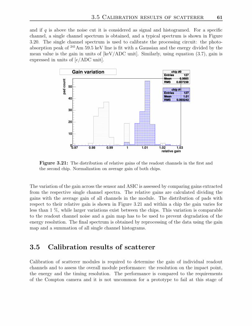
3.5 Calibration results of scatterer 61
and if q is above the noise cut it is considered as signal and histogramed. For a specificchannel, a single channel spectrum is obtained, and a typical spectrum is shown in Figure3.20. The single channel spectrum is used to calibrate the processing circuit: the photo-absorption peak of 241Am 59.5 keV line is fit with a Gaussian and the energy divided by themean value is the gain in units of [keV/ADC unit]. Similarly, using equation (3.7), gain isexpressed in units of [e/ADC unit].
chip #0Entries 127Mean 0.9885RMS 0.007238
relative gain0.97 0.98 0.99 1 1.01 1.02 1.03
pad
coun
t
0
10
20
30
40
50
chip #0Entries 127Mean 0.9885RMS 0.007238
Gain variation
chip #1Entries 127Mean 1.01RMS 0.003242
chip #1Entries 127Mean 1.01RMS 0.003242
chip #1Entries 127Mean 1.01RMS 0.003242
Figure 3.21: The distribution of relative gains of the readout channels in the first andthe second chip. Normalization on average gain of both chips.
The variation of the gain across the sensor and ASIC is assessed by comparing gains extractedfrom the respective single channel spectra. The relative gains are calculated dividing thegains with the average gain of all channels in the module. The distribution of pads withrespect to their relative gain is shown in Figure 3.21 and within a chip the gain varies forless than 1 %, while larger variations exist between the chips. This variation is comparableto the readout channel noise and a gain map has to be used to prevent degradation of theenergy resolution. The final spectrum is obtained by reprocessing of the data using the gainmap and a summation of all single channel histograms.
3.5 Calibration results of scatterer
Calibration of scatterer modules is required to determine the gain of individual readoutchannels and to assess the overall module performance: the resolution on the impact point,the energy and the timing resolution. The performance is compared to the requirementsof the Compton camera and it is not uncommon for a prototype to fail at this stage of
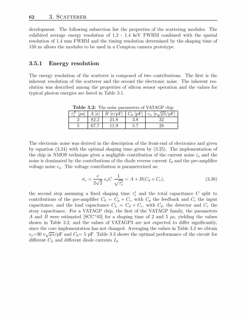
62 3. Scatterer
development. The following subsection list the properties of the scattering modules. Theexhibited average energy resolution of 1.2 - 1.4 keV FWHM combined with the spatialresolution of 1.4 mm FWHM and the timing resolution determined by the shaping time of150 ns allows the modules to be used in a Compton camera prototype.
3.5.1 Energy resolution
The energy resolution of the scatterer is composed of two contributions. The first is theinherent resolution of the scatterer and the second the electronic noise. The inherent res-olution was described among the properties of silicon sensor operation and the values fortypical photon energies are listed in Table 3.1.
Table 3.2: The noise parameters of VATAGP chip
τEs [µs] A [e] B [e/pF] C0 [pF] ea [e
õs/pF]
2 82.2 21.8 3.8 325 67.7 11.9 5.7 28
The electronic noise was derived in the description of the front-end of electronics and givenby equation (3.24) with the optimal shaping time given by (3.25). The implementation ofthe chip in NMOS technique gives a negligible contribution of the current noise ia and thenoise is dominated by the contributions of the diode reverse current Id and the pre-amplifiervoltage noise ea. The voltage contribution is parameterized as:
σv =e
2√
2eaC
1√
τ ts
= A + B(Cd + Cr), (3.38)
the second step assuming a fixed shaping time τ ts and the total capacitance C split to
contributions of the pre-amplifier C0 = Cp + Ci, with Cp the feedback and Ci the inputcapacitance, and the load capacitance CL = Cd + Cr, with Cd, the detector and Cr thestray capacitance. For a VATAGP chip, the first of the VATAGP family, the parametersA and B were estimated [SCC+03] for a shaping time of 2 and 5 µs, yielding the valuesshown in Table 3.2, and the values of VATAGP3 are not expected to differ significantly,since the core implementation has not changed. Averaging the values in Table 3.2 we obtainea=30 e
õs/pF and C0= 5 pF. Table 3.3 shows the optimal performance of the circuit for
different CL and different diode currents Id.

3.5 Calibration results of scatterer 63
Table 3.3: Optimum performance of a VATAGP chip for different input capacitancesand diode currents.
Capacitance Id [pF] τEs [µs] σE
n [e] 241Am resolution(Cd + Cr) [pF] σT
n [e ENC] FWHME [keV]0.5 100 4.6 104 112 0.952 100 5.9 117 124 1.05
0.5 200 3.3 123 130 1.102 200 4.2 140 145 1.23
The total resolution includes the contribution of the statistical fluctuation of the ionizedcharge (equation (3.8)) equal to 41 e for photo-electrons created by initial photon withenergy of 59.5 keV, which was used for calibration. The energy resolution is derived fromthe ENC using equation (3.22).
Table 3.4: Emission spectrum of 241Am showing γ and X-ray emission with relativeintensity exceeding 0.1 %.
Energy [keV] emission type Relative intensity [%]13.761 X-ray (Np Lα,2) 1.0713.946 X-ray (Np Lα,1) 9.615.861 X-ray (Np Lh 0.15316.109 X-ray (Np Lβ,6) 0.18416.816 X-ray (Np Lβ,2) 2.517.061 X-ray (Np Lβ,4) 1.517.505 X-ray (Np Lβ,5) 0.6517.751 X-ray (Np Lβ,1) 5.717.992 X-ray (Np Lβ,3) 1.3720.784 X-ray (Np Lγ,1) 1.3921.099 X-ray (Np Lγ,2) 0.6521.342 X-ray (Np Lγ,3) 0.5921.491 X-ray (Np Lγ,6) 0.2926.3448 γ-ray 2.4033.1964 γ-ray 0.12659.5412 γ-ray 35.9
The energy resolution of the scatterer was measured using 241Am, a γ-ray source with theprincipal photon energy equal to 59.5 keV. The α particles, which are also emitted by thesource are absorbed in the air before they reach the sensor. The DAQ setup shown in Figure3.17 was used. The sensor was shielded from ambient radio-frequency noise in a metal box,
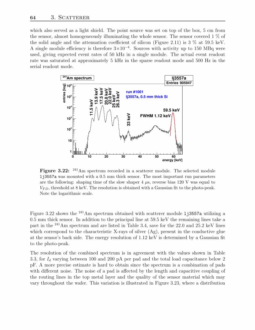
64 3. Scatterer
which also served as a light shield. The point source was set on top of the box, 5 cm fromthe sensor, almost homogeneously illuminating the whole sensor. The sensor covered 1 % ofthe solid angle and the attenuation coefficient of silicon (Figure 2.11) is 3 % at 59.5 keV.A single module efficiency is therefore 3×10⁻⁴. Sources with activity up to 150 MBq wereused, giving expected event rates of 50 kHz in a single module. The actual event readoutrate was saturated at approximately 5 kHz in the sparse readout mode and 500 Hz in theserial readout mode.
lj3557aEntries 905947
energy [keV]0 10 20 30 40 50 60
entr
ies
[log]
1
10
210
310
410
510
610
lj3557aEntries 905947
Am spectrum241
11.5
keV 13
.9 k
eV17
.5 k
eV20
.8 k
eV22
.0 k
eV25
keV
26.3
keV
33 k
eV
59.5 keVFWHM 1.12 keV
lj3557a, 0.5 mm thick Sirun #1001
Figure 3.22: 241Am spectrum recorded in a scatterer module. The selected modulelj3557a was mounted with a 0.5 mm thick sensor. The most important run parametersare the following: shaping time of the slow shaper 4 µs, reverse bias 120 V was equal toVFD, threshold at 8 keV. The resolution is obtained with a Gaussian fit to the photo-peak.Note the logarithmic scale.
Figure 3.22 shows the 241Am spectrum obtained with scatterer module lj3557a utilizing a0.5 mm thick sensor. In addition to the principal line at 59.5 keV the remaining lines take apart in the 241Am spectrum and are listed in Table 3.4, save for the 22.0 and 25.2 keV lineswhich correspond to the characteristic X-rays of silver (Ag), present in the conductive glueat the sensor’s back side. The energy resolution of 1.12 keV is determined by a Gaussian fitto the photo-peak.
The resolution of the combined spectrum is in agreement with the values shown in Table3.3, for Id varying between 100 and 200 pA per pad and the total load capacitance below 2pF. A more precise estimate is hard to obtain since the spectrum is a combination of padswith different noise. The noise of a pad is affected by the length and capacitive coupling ofthe routing lines in the top metal layer and the quality of the sensor material which mayvary throughout the wafer. This variation is illustrated in Figure 3.23, where a distribution
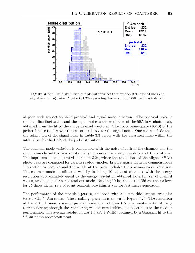
3.5 Calibration results of scatterer 65
Am peak241
Entries 232Mean 137.9RMS 16.02
ENC [e]80 100 120 140 160 180 200 220 240
pad
dist
ribu
tion
[arb
]
0
5
10
15
20
25
30
35
40
45Am peak241
Entries 232Mean 137.9RMS 16.02
Noise distribution
pedestalEntries 232Mean 118.4RMS 12.9
pedestalEntries 232Mean 118.4RMS 12.9
pedestalEntries 232Mean 118.4RMS 12.9
run #1001
Figure 3.23: The distribution of pads with respect to their pedestal (dashed line) andsignal (solid line) noise. A subset of 232 operating channels out of 256 available is drawn.
of pads with respect to their pedestal and signal noise is shown. The pedestal noise isthe base-line fluctuation and the signal noise is the resolution of the 59.5 keV photo-peak,obtained from the fit to the single channel spectrum. The root-mean-square (RMS) of thepedestal noise is 12 e over the sensor, and 16 e for the signal noise. One can conclude thatthe estimation of the signal noise in Table 3.3 agrees with the measured noise within theinterval set by the RMS of the pad distribution.
The common mode variation is comparable with the noise of each of the channels and thecommon-mode subtraction substantially improves the energy resolution of the scatterer.The improvement is illustrated in Figure 3.24, where the resolutions of the aligned 241Amphoto-peak are compared for various readout-modes. In pure sparse mode no common-modesubtraction is possible and the width of the peak includes the common-mode variation.The common-mode is estimated well by including 10 adjacent channels, with the energyresolution approximately equal to the energy resolution obtained for a full set of channelvalues, available in the serial read-out mode. Reading 10 instead of the 256 channels allowsfor 25-times higher rate of event readout, providing a way for fast image generation.
The performance of the module lj3557b, equipped with a 1 mm thick sensor, was alsotested with 241Am source. The resulting spectrum is shown in Figure 3.25. The resolutionof 1 mm thick sensors was in general worse than of their 0.5 mm counterparts. A largecurrent flowing through the guard ring was observed which might deteriorate the moduleperformance. The average resolution was 1.4 keV FWHM, obtained by a Gaussian fit to the241Am photo-absorption peak.
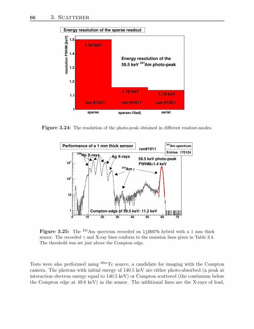
66 3. Scatterer
sparse sparse+10adj serial
reso
lutio
n FW
HM
[keV
]
1
1.1
1.2
1.3
1.4
1.5
Energy resolution of the sparse readout
1.50 keV
1.16 keV 1.14 keV
Am photo-peak24159.5 keV
run #1001run #1011run #1021
Energy resolution of the
Figure 3.24: The resolution of the photo-peak obtained in different readout-modes.
Am spectrum241
Entries 170124
0 10 20 30 40 50 60 70
1
10
210
310
Am spectrum241
Entries 170124
Performance of a 1 mm thick sensor
59.5 keV photo-peakFWHM=1.4 keV
Compton edge of 59.5 keV: 11.2 keV
Np X-rays239Ag X-rays
γAm 241
run#1011
Figure 3.25: The 241Am spectrum recorded on lj3557b hybrid with a 1 mm thicksensor. The recorded γ and X-ray lines conform to the emission lines given in Table 3.4.The threshold was set just above the Compton edge.
Tests were also performed using 99mTc source, a candidate for imaging with the Comptoncamera. The photons with initial energy of 140.5 keV are either photo-absorbed (a peak atinteraction electron energy equal to 140.5 keV) or Compton scattered (the continuum belowthe Compton edge at 49.8 keV) in the sensor. The additional lines are the X-rays of lead,
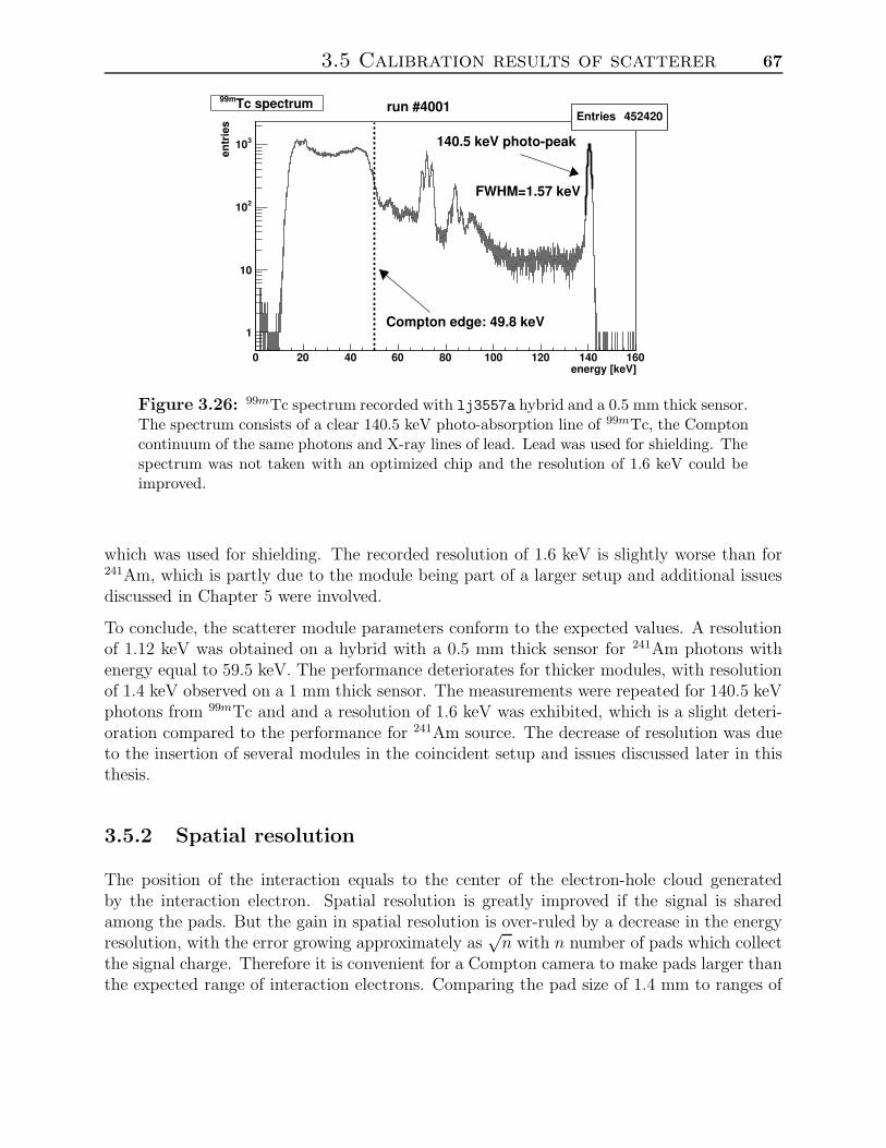
3.5 Calibration results of scatterer 67
Entries 452420
energy [keV]0 20 40 60 80 100 120 140 160
entr
ies
1
10
210
310
Entries 452420Tc spectrum99m
run #4001
FWHM=1.57 keV
140.5 keV photo-peak
Compton edge: 49.8 keV
Figure 3.26: 99mTc spectrum recorded with lj3557a hybrid and a 0.5 mm thick sensor.The spectrum consists of a clear 140.5 keV photo-absorption line of 99mTc, the Comptoncontinuum of the same photons and X-ray lines of lead. Lead was used for shielding. Thespectrum was not taken with an optimized chip and the resolution of 1.6 keV could beimproved.
which was used for shielding. The recorded resolution of 1.6 keV is slightly worse than for241Am, which is partly due to the module being part of a larger setup and additional issuesdiscussed in Chapter 5 were involved.
To conclude, the scatterer module parameters conform to the expected values. A resolutionof 1.12 keV was obtained on a hybrid with a 0.5 mm thick sensor for 241Am photons withenergy equal to 59.5 keV. The performance deteriorates for thicker modules, with resolutionof 1.4 keV observed on a 1 mm thick sensor. The measurements were repeated for 140.5 keVphotons from 99mTc and and a resolution of 1.6 keV was exhibited, which is a slight deteri-oration compared to the performance for 241Am source. The decrease of resolution was dueto the insertion of several modules in the coincident setup and issues discussed later in thisthesis.
3.5.2 Spatial resolution
The position of the interaction equals to the center of the electron-hole cloud generatedby the interaction electron. Spatial resolution is greatly improved if the signal is sharedamong the pads. But the gain in spatial resolution is over-ruled by a decrease in the energyresolution, with the error growing approximately as
√n with n number of pads which collect
the signal charge. Therefore it is convenient for a Compton camera to make pads larger thanthe expected range of interaction electrons. Comparing the pad size of 1.4 mm to ranges of
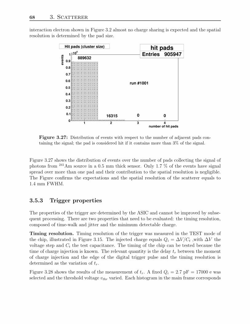
68 3. Scatterer
interaction electron shown in Figure 3.2 almost no charge sharing is expected and the spatialresolution is determined by the pad size.
hit padsEntries 905947
number of hit pads1 2 3 4
even
ts
0
0.1
0.2
0.3
0.4
0.5
0.6
0.7
0.8
0.9
1610×
hit padsEntries 905947
Hit pads (cluster size)
889632
16315 0 0
run #1001
Figure 3.27: Distribution of events with respect to the number of adjacent pads con-taining the signal; the pad is considered hit if it contains more than 3% of the signal.
Figure 3.27 shows the distribution of events over the number of pads collecting the signal ofphotons from 241Am source in a 0.5 mm thick sensor. Only 1.7 % of the events have signalspread over more than one pad and their contribution to the spatial resolution is negligible.The Figure confirms the expectations and the spatial resolution of the scatterer equals to1.4 mm FWHM.
3.5.3 Trigger properties
The properties of the trigger are determined by the ASIC and cannot be improved by subse-quent processing. There are two properties that need to be evaluated: the timing resolution,composed of time-walk and jitter and the minimum detectable charge.
Timing resolution. Timing resolution of the trigger was measured in the TEST mode ofthe chip, illustrated in Figure 3.15. The injected charge equals Qi = ∆V/Ct ,with ∆V thevoltage step and Ct the test capacitance. The timing of the chip can be tested because thetime of charge injection is known. The relevant quantity is the delay tr between the momentof charge injection and the edge of the digital trigger pulse and the timing resolution isdetermined as the variation of tr.
Figure 3.28 shows the results of the measurement of tr. A fixed Qi = 2.7 pF = 17000 e wasselected and the threshold voltage vthr varied. Each histogram in the main frame corresponds
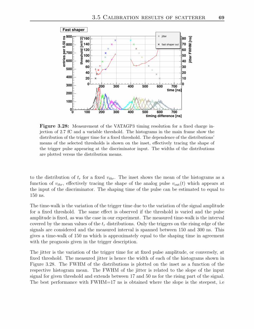
3.5 Calibration results of scatterer 69
timing difference [ns]0 100 200 300 400 500 600 700
entr
ies
per
0.50
ns
0
100
200
300
400
500
600
700
800
900
Fast shaper
jitte
r FW
HM
[ns]
010
20
30
4050
6070
80
thre
shol
d [m
V/2
] 0
20
40
60
80100
120140
160
time [ns]200 300 400 500 600 700
jitter
fast shaper out
Figure 3.28: Measurement of the VATAGP3 timing resolution for a fixed charge in-jection of 2.7 fC and a variable threshold. The histograms in the main frame show thedistribution of the trigger time for a fixed threshold. The dependence of the distributions’means of the selected thresholds is shown on the inset, effectively tracing the shape ofthe trigger pulse appearing at the discriminator input. The widths of the distributionsare plotted versus the distribution means.
to the distribution of tr for a fixed vthr. The inset shows the mean of the histograms as afunction of vthr, effectively tracing the shape of the analog pulse vout(t) which appears atthe input of the discriminator. The shaping time of the pulse can be estimated to equal to150 ns.
The time-walk is the variation of the trigger time due to the variation of the signal amplitudefor a fixed threshold. The same effect is observed if the threshold is varied and the pulseamplitude is fixed, as was the case in our experiment. The measured time-walk is the intervalcovered by the mean values of the tr distributions. Only the triggers on the rising edge of thesignals are considered and the measured interval is spanned between 150 and 300 ns. Thisgives a time-walk of 150 ns which is approximately equal to the shaping time in agreementwith the prognosis given in the trigger description.
The jitter is the variation of the trigger time for at fixed pulse amplitude, or conversely, atfixed threshold. The measured jitter is hence the width of each of the histograms shown inFigure 3.28. The FWHM of the distributions is plotted on the inset as a function of therespective histogram mean. The FWHM of the jitter is related to the slope of the inputsignal for given threshold and extends between 17 and 50 ns for the rising part of the signal.The best performance with FWHM=17 ns is obtained where the slope is the steepest, i.e
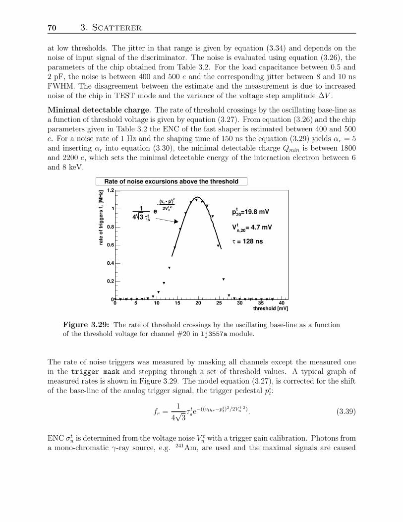
70 3. Scatterer
at low thresholds. The jitter in that range is given by equation (3.34) and depends on thenoise of input signal of the discriminator. The noise is evaluated using equation (3.26), theparameters of the chip obtained from Table 3.2. For the load capacitance between 0.5 and2 pF, the noise is between 400 and 500 e and the corresponding jitter between 8 and 10 nsFWHM. The disagreement between the estimate and the measurement is due to increasednoise of the chip in TEST mode and the variance of the voltage step amplitude ∆V .
Minimal detectable charge. The rate of threshold crossings by the oscillating base-line asa function of threshold voltage is given by equation (3.27). From equation (3.26) and the chipparameters given in Table 3.2 the ENC of the fast shaper is estimated between 400 and 500e. For a noise rate of 1 Hz and the shaping time of 150 ns the equation (3.29) yields αr = 5and inserting αr into equation (3.30), the minimal detectable charge Qmin is between 1800and 2200 e, which sets the minimal detectable energy of the interaction electron between 6and 8 keV.
threshold [mV]0 5 10 15 20 25 30 35 40
[MH
z]r
rate
of t
rigg
ers
f
0
0.2
0.4
0.6
0.8
1
1.2
Rate of noise excursions above the threshold
=19.8 mV20tp
= 4.7 mVtn,20V
= 128 nsτ
t 2n2V
2)t - pt(v
-
etsτ 34
1
Figure 3.29: The rate of threshold crossings by the oscillating base-line as a functionof the threshold voltage for channel #20 in lj3557a module.
The rate of noise triggers was measured by masking all channels except the measured onein the trigger mask and stepping through a set of threshold values. A typical graph ofmeasured rates is shown in Figure 3.29. The model equation (3.27), is corrected for the shiftof the base-line of the analog trigger signal, the trigger pedestal pi
t:
fr =1
4√
3τ tse
−((vthr−pit)
2/2V t 2n ). (3.39)
ENC σtn is determined from the voltage noise V t
n with a trigger gain calibration. Photons froma mono-chromatic γ-ray source, e.g. 241Am, are used and the maximal signals are caused
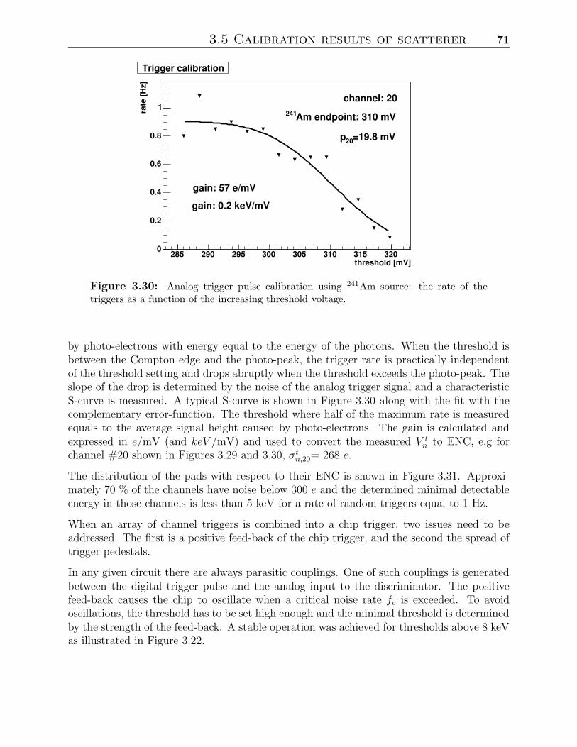
3.5 Calibration results of scatterer 71
threshold [mV]285 290 295 300 305 310 315 320
rate
[Hz]
0
0.2
0.4
0.6
0.8
1
Trigger calibration
channel: 20
Am endpoint: 310 mV241
=19.8 mV20p
gain: 57 e/mV
gain: 0.2 keV/mV
Figure 3.30: Analog trigger pulse calibration using 241Am source: the rate of thetriggers as a function of the increasing threshold voltage.
by photo-electrons with energy equal to the energy of the photons. When the threshold isbetween the Compton edge and the photo-peak, the trigger rate is practically independentof the threshold setting and drops abruptly when the threshold exceeds the photo-peak. Theslope of the drop is determined by the noise of the analog trigger signal and a characteristicS-curve is measured. A typical S-curve is shown in Figure 3.30 along with the fit with thecomplementary error-function. The threshold where half of the maximum rate is measuredequals to the average signal height caused by photo-electrons. The gain is calculated andexpressed in e/mV (and keV /mV) and used to convert the measured V t
n to ENC, e.g forchannel #20 shown in Figures 3.29 and 3.30, σt
n,20= 268 e.
The distribution of the pads with respect to their ENC is shown in Figure 3.31. Approxi-mately 70 % of the channels have noise below 300 e and the determined minimal detectableenergy in those channels is less than 5 keV for a rate of random triggers equal to 1 Hz.
When an array of channel triggers is combined into a chip trigger, two issues need to beaddressed. The first is a positive feed-back of the chip trigger, and the second the spread oftrigger pedestals.
In any given circuit there are always parasitic couplings. One of such couplings is generatedbetween the digital trigger pulse and the analog input to the discriminator. The positivefeed-back causes the chip to oscillate when a critical noise rate fc is exceeded. To avoidoscillations, the threshold has to be set high enough and the minimal threshold is determinedby the strength of the feed-back. A stable operation was achieved for thresholds above 8 keVas illustrated in Figure 3.22.
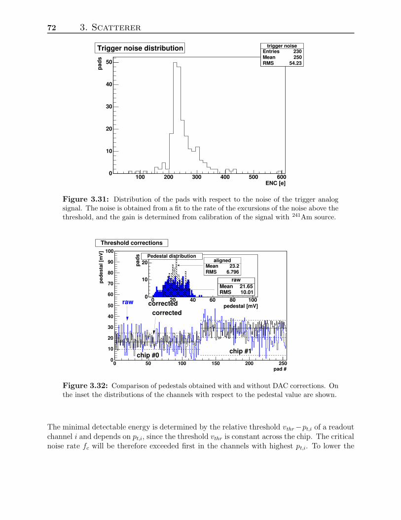
72 3. Scatterer
trigger noiseEntries 230Mean 250RMS 54.23
ENC [e]100 200 300 400 500 600
pads
0
10
20
30
40
50
trigger noiseEntries 230Mean 250RMS 54.23
Trigger noise distribution
Figure 3.31: Distribution of the pads with respect to the noise of the trigger analogsignal. The noise is obtained from a fit to the rate of the excursions of the noise above thethreshold, and the gain is determined from calibration of the signal with 241Am source.
pad #0 50 100 150 200 250
pede
stal
[mV
]
0
10
20
30
40
50
60
70
80
90
100
Threshold corrections
rawMean 21.65RMS 10.01
pedestal [mV]0 20 40 60 80 100
pads
0
10
20
rawMean 21.65RMS 10.01
Pedestal distributionaligned
Mean 23.2RMS 6.796
alignedMean 23.2RMS 6.796
alignedMean 23.2RMS 6.796
correctedcorrected
raw
chip #0 chip #1
Figure 3.32: Comparison of pedestals obtained with and without DAC corrections. Onthe inset the distributions of the channels with respect to the pedestal value are shown.
The minimal detectable energy is determined by the relative threshold vthr−pt,i of a readoutchannel i and depends on pt,i, since the threshold vthr is constant across the chip. The criticalnoise rate fc will be therefore exceeded first in the channels with highest pt,i. To lower the
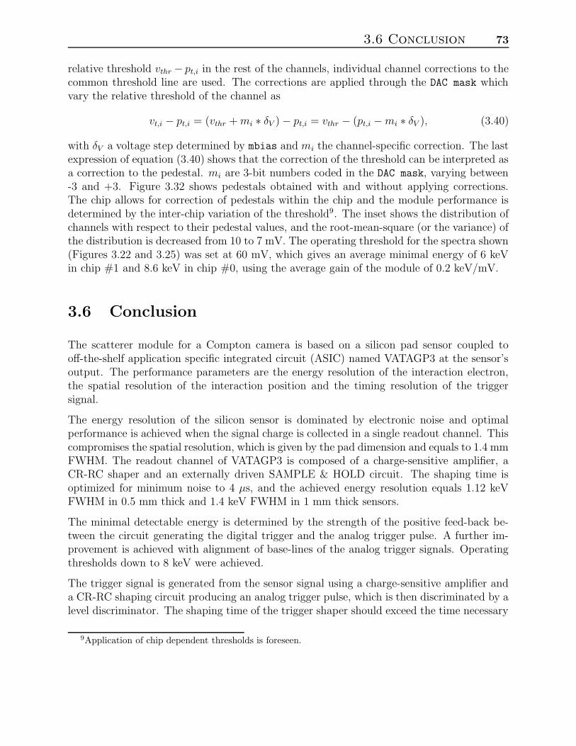
3.6 Conclusion 73
relative threshold vthr − pt,i in the rest of the channels, individual channel corrections to thecommon threshold line are used. The corrections are applied through the DAC mask whichvary the relative threshold of the channel as
vt,i − pt,i = (vthr + mi ∗ δV ) − pt,i = vthr − (pt,i − mi ∗ δV ), (3.40)
with δV a voltage step determined by mbias and mi the channel-specific correction. The lastexpression of equation (3.40) shows that the correction of the threshold can be interpreted asa correction to the pedestal. mi are 3-bit numbers coded in the DAC mask, varying between-3 and +3. Figure 3.32 shows pedestals obtained with and without applying corrections.The chip allows for correction of pedestals within the chip and the module performance isdetermined by the inter-chip variation of the threshold9. The inset shows the distribution ofchannels with respect to their pedestal values, and the root-mean-square (or the variance) ofthe distribution is decreased from 10 to 7 mV. The operating threshold for the spectra shown(Figures 3.22 and 3.25) was set at 60 mV, which gives an average minimal energy of 6 keVin chip #1 and 8.6 keV in chip #0, using the average gain of the module of 0.2 keV/mV.
3.6 Conclusion
The scatterer module for a Compton camera is based on a silicon pad sensor coupled tooff-the-shelf application specific integrated circuit (ASIC) named VATAGP3 at the sensor’soutput. The performance parameters are the energy resolution of the interaction electron,the spatial resolution of the interaction position and the timing resolution of the triggersignal.
The energy resolution of the silicon sensor is dominated by electronic noise and optimalperformance is achieved when the signal charge is collected in a single readout channel. Thiscompromises the spatial resolution, which is given by the pad dimension and equals to 1.4 mmFWHM. The readout channel of VATAGP3 is composed of a charge-sensitive amplifier, aCR-RC shaper and an externally driven SAMPLE & HOLD circuit. The shaping time isoptimized for minimum noise to 4 µs, and the achieved energy resolution equals 1.12 keVFWHM in 0.5 mm thick and 1.4 keV FWHM in 1 mm thick sensors.
The minimal detectable energy is determined by the strength of the positive feed-back be-tween the circuit generating the digital trigger and the analog trigger pulse. A further im-provement is achieved with alignment of base-lines of the analog trigger signals. Operatingthresholds down to 8 keV were achieved.
The trigger signal is generated from the sensor signal using a charge-sensitive amplifier anda CR-RC shaping circuit producing an analog trigger pulse, which is then discriminated by alevel discriminator. The shaping time of the trigger shaper should exceed the time necessary
9Application of chip dependent thresholds is foreseen.

74 3. Scatterer
to collect the charge. The time varies with the interaction depth in the sensor and, forvoltages below 2VFD foreseen for the module operation, equals up to 70 ns. The shapingtime of the trigger is set to 150 ns. There are two contributions to the timing resolution ofthe trigger: the time-walk which equals to the shaping time and the jitter, which equals to afraction of the shaping-time, the fraction determined by the ratio of the signal and the noiseof the analog trigger pulse. Because the minimal detectable signal must exceed the triggernoise by a factor, the timing resolution is dominated by the time walk.
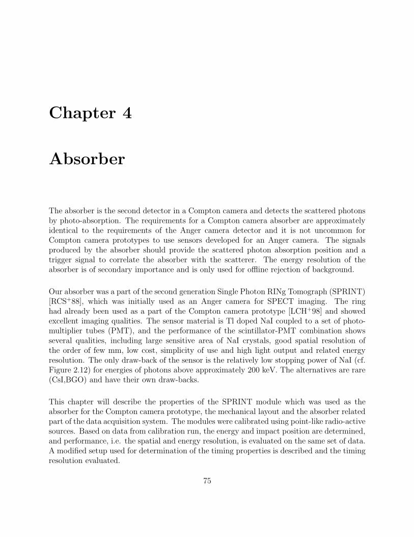
Chapter 4
Absorber
The absorber is the second detector in a Compton camera and detects the scattered photonsby photo-absorption. The requirements for a Compton camera absorber are approximatelyidentical to the requirements of the Anger camera detector and it is not uncommon forCompton camera prototypes to use sensors developed for an Anger camera. The signalsproduced by the absorber should provide the scattered photon absorption position and atrigger signal to correlate the absorber with the scatterer. The energy resolution of theabsorber is of secondary importance and is only used for offline rejection of background.
Our absorber was a part of the second generation Single Photon RINg Tomograph (SPRINT)[RCS+88], which was initially used as an Anger camera for SPECT imaging. The ringhad already been used as a part of the Compton camera prototype [LCH+98] and showedexcellent imaging qualities. The sensor material is Tl doped NaI coupled to a set of photo-multiplier tubes (PMT), and the performance of the scintillator-PMT combination showsseveral qualities, including large sensitive area of NaI crystals, good spatial resolution ofthe order of few mm, low cost, simplicity of use and high light output and related energyresolution. The only draw-back of the sensor is the relatively low stopping power of NaI (cf.Figure 2.12) for energies of photons above approximately 200 keV. The alternatives are rare(CsI,BGO) and have their own draw-backs.
This chapter will describe the properties of the SPRINT module which was used as theabsorber for the Compton camera prototype, the mechanical layout and the absorber relatedpart of the data acquisition system. The modules were calibrated using point-like radio-activesources. Based on data from calibration run, the energy and impact position are determined,and performance, i.e. the spatial and energy resolution, is evaluated on the same set of data.A modified setup used for determination of the timing properties is described and the timingresolution evaluated.
75
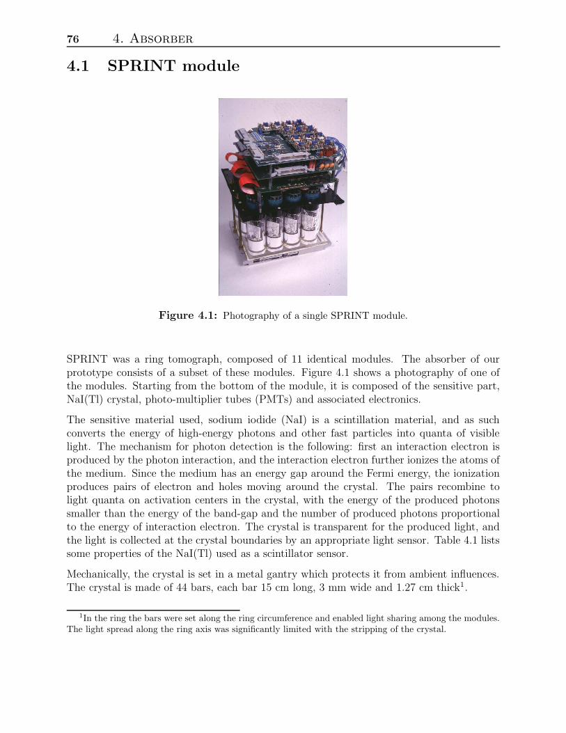
76 4. Absorber
4.1 SPRINT module
Figure 4.1: Photography of a single SPRINT module.
SPRINT was a ring tomograph, composed of 11 identical modules. The absorber of ourprototype consists of a subset of these modules. Figure 4.1 shows a photography of one ofthe modules. Starting from the bottom of the module, it is composed of the sensitive part,NaI(Tl) crystal, photo-multiplier tubes (PMTs) and associated electronics.
The sensitive material used, sodium iodide (NaI) is a scintillation material, and as suchconverts the energy of high-energy photons and other fast particles into quanta of visiblelight. The mechanism for photon detection is the following: first an interaction electron isproduced by the photon interaction, and the interaction electron further ionizes the atoms ofthe medium. Since the medium has an energy gap around the Fermi energy, the ionizationproduces pairs of electron and holes moving around the crystal. The pairs recombine tolight quanta on activation centers in the crystal, with the energy of the produced photonssmaller than the energy of the band-gap and the number of produced photons proportionalto the energy of interaction electron. The crystal is transparent for the produced light, andthe light is collected at the crystal boundaries by an appropriate light sensor. Table 4.1 listssome properties of the NaI(Tl) used as a scintillator sensor.
Mechanically, the crystal is set in a metal gantry which protects it from ambient influences.The crystal is made of 44 bars, each bar 15 cm long, 3 mm wide and 1.27 cm thick1.
1In the ring the bars were set along the ring circumference and enabled light sharing among the modules.The light spread along the ring axis was significantly limited with the stripping of the crystal.
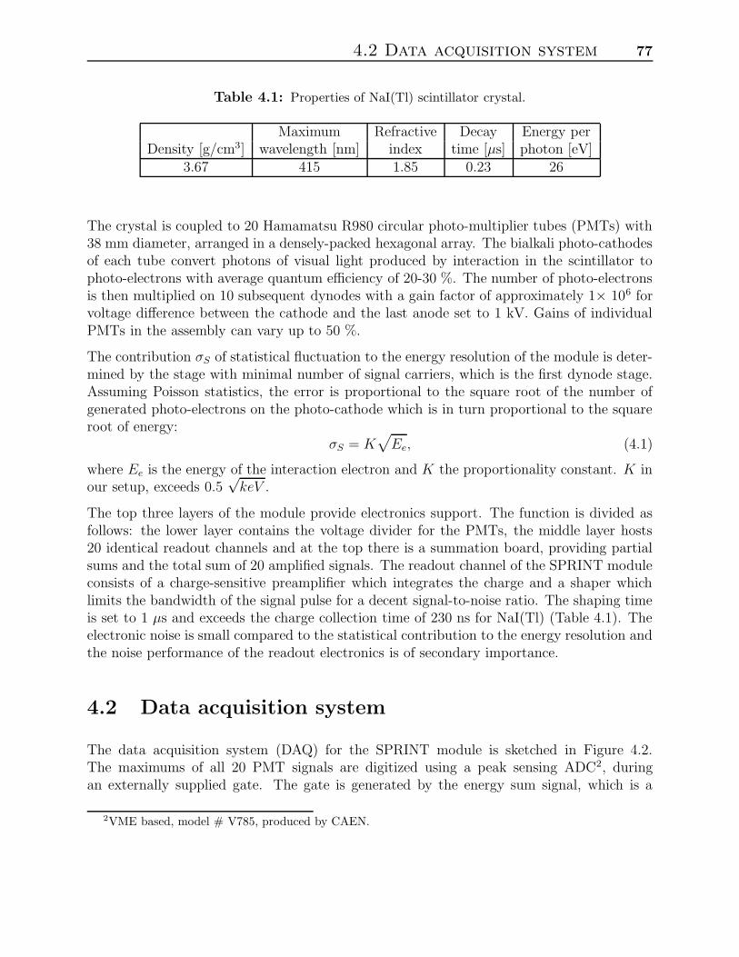
4.2 Data acquisition system 77
Table 4.1: Properties of NaI(Tl) scintillator crystal.
Maximum Refractive Decay Energy perDensity [g/cm3] wavelength [nm] index time [µs] photon [eV]
3.67 415 1.85 0.23 26
The crystal is coupled to 20 Hamamatsu R980 circular photo-multiplier tubes (PMTs) with38 mm diameter, arranged in a densely-packed hexagonal array. The bialkali photo-cathodesof each tube convert photons of visual light produced by interaction in the scintillator tophoto-electrons with average quantum efficiency of 20-30 %. The number of photo-electronsis then multiplied on 10 subsequent dynodes with a gain factor of approximately 1× 10⁶ forvoltage difference between the cathode and the last anode set to 1 kV. Gains of individualPMTs in the assembly can vary up to 50 %.
The contribution σS of statistical fluctuation to the energy resolution of the module is deter-mined by the stage with minimal number of signal carriers, which is the first dynode stage.Assuming Poisson statistics, the error is proportional to the square root of the number ofgenerated photo-electrons on the photo-cathode which is in turn proportional to the squareroot of energy:
σS = K√
Ee, (4.1)
where Ee is the energy of the interaction electron and K the proportionality constant. K inour setup, exceeds 0.5
√keV .
The top three layers of the module provide electronics support. The function is divided asfollows: the lower layer contains the voltage divider for the PMTs, the middle layer hosts20 identical readout channels and at the top there is a summation board, providing partialsums and the total sum of 20 amplified signals. The readout channel of the SPRINT moduleconsists of a charge-sensitive preamplifier which integrates the charge and a shaper whichlimits the bandwidth of the signal pulse for a decent signal-to-noise ratio. The shaping timeis set to 1 µs and exceeds the charge collection time of 230 ns for NaI(Tl) (Table 4.1). Theelectronic noise is small compared to the statistical contribution to the energy resolution andthe noise performance of the readout electronics is of secondary importance.
4.2 Data acquisition system
The data acquisition system (DAQ) for the SPRINT module is sketched in Figure 4.2.The maximums of all 20 PMT signals are digitized using a peak sensing ADC2, duringan externally supplied gate. The gate is generated by the energy sum signal, which is a
2VME based, model # V785, produced by CAEN.
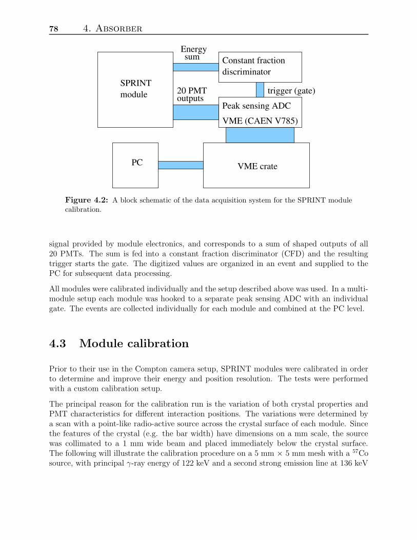
78 4. Absorber
PC
Peak sensing ADC
VME (CAEN V785)
VME crate
20 PMT outputs
Constant fractiondiscriminator
sumEnergy
SPRINTmodule trigger (gate)
Figure 4.2: A block schematic of the data acquisition system for the SPRINT modulecalibration.
signal provided by module electronics, and corresponds to a sum of shaped outputs of all20 PMTs. The sum is fed into a constant fraction discriminator (CFD) and the resultingtrigger starts the gate. The digitized values are organized in an event and supplied to thePC for subsequent data processing.
All modules were calibrated individually and the setup described above was used. In a multi-module setup each module was hooked to a separate peak sensing ADC with an individualgate. The events are collected individually for each module and combined at the PC level.
4.3 Module calibration
Prior to their use in the Compton camera setup, SPRINT modules were calibrated in orderto determine and improve their energy and position resolution. The tests were performedwith a custom calibration setup.
The principal reason for the calibration run is the variation of both crystal properties andPMT characteristics for different interaction positions. The variations were determined bya scan with a point-like radio-active source across the crystal surface of each module. Sincethe features of the crystal (e.g. the bar width) have dimensions on a mm scale, the sourcewas collimated to a 1 mm wide beam and placed immediately below the crystal surface.The following will illustrate the calibration procedure on a 5 mm × 5 mm mesh with a 57Cosource, with principal γ-ray energy of 122 keV and a second strong emission line at 136 keV
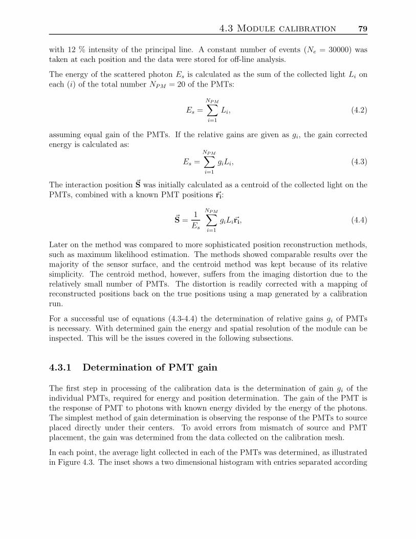
4.3 Module calibration 79
with 12 % intensity of the principal line. A constant number of events (Ne = 30000) wastaken at each position and the data were stored for off-line analysis.
The energy of the scattered photon Es is calculated as the sum of the collected light Li oneach (i) of the total number NPM = 20 of the PMTs:
Es =
NPM∑
i=1
Li, (4.2)
assuming equal gain of the PMTs. If the relative gains are given as gi, the gain correctedenergy is calculated as:
Es =
NPM∑
i=1
giLi, (4.3)
The interaction position ~S was initially calculated as a centroid of the collected light on thePMTs, combined with a known PMT positions ~ri:
~S =1
Es
NPM∑
i=1
giLi~ri, (4.4)
Later on the method was compared to more sophisticated position reconstruction methods,such as maximum likelihood estimation. The methods showed comparable results over themajority of the sensor surface, and the centroid method was kept because of its relativesimplicity. The centroid method, however, suffers from the imaging distortion due to therelatively small number of PMTs. The distortion is readily corrected with a mapping ofreconstructed positions back on the true positions using a map generated by a calibrationrun.
For a successful use of equations (4.3-4.4) the determination of relative gains gi of PMTsis necessary. With determined gain the energy and spatial resolution of the module can beinspected. This will be the issues covered in the following subsections.
4.3.1 Determination of PMT gain
The first step in processing of the calibration data is the determination of gain gi of theindividual PMTs, required for energy and position determination. The gain of the PMT isthe response of PMT to photons with known energy divided by the energy of the photons.The simplest method of gain determination is observing the response of the PMTs to sourceplaced directly under their centers. To avoid errors from mismatch of source and PMTplacement, the gain was determined from the data collected on the calibration mesh.
In each point, the average light collected in each of the PMTs was determined, as illustratedin Figure 4.3. The inset shows a two dimensional histogram with entries separated according
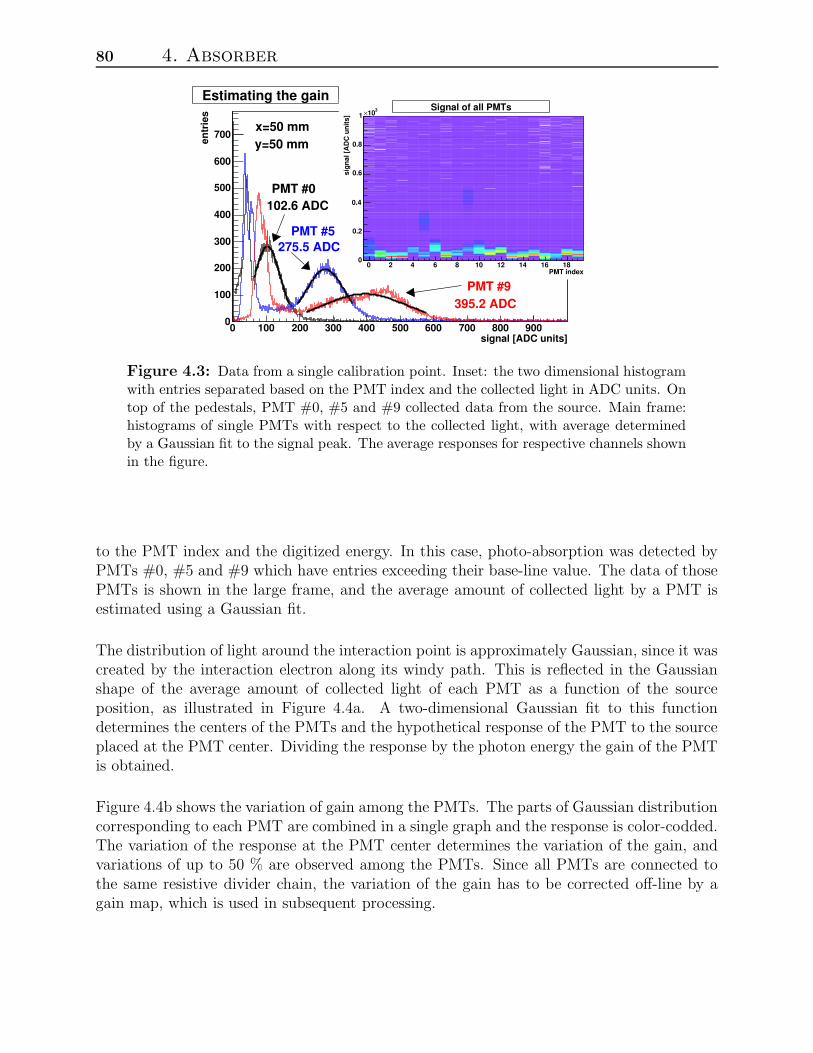
80 4. Absorber
signal [ADC units]0 100 200 300 400 500 600 700 800 900
entr
ies
0
100
200
300
400
500
600
700
Estimating the gain
PMT index0 2 4 6 8 10 12 14 16 18
sign
al [A
DC
uni
ts]
0
0.2
0.4
0.6
0.8
1310×
Signal of all PMTs
PMT #0102.6 ADC
PMT #5275.5 ADC
PMT #9395.2 ADC
x=50 mmy=50 mm
Figure 4.3: Data from a single calibration point. Inset: the two dimensional histogramwith entries separated based on the PMT index and the collected light in ADC units. Ontop of the pedestals, PMT #0, #5 and #9 collected data from the source. Main frame:histograms of single PMTs with respect to the collected light, with average determinedby a Gaussian fit to the signal peak. The average responses for respective channels shownin the figure.
to the PMT index and the digitized energy. In this case, photo-absorption was detected byPMTs #0, #5 and #9 which have entries exceeding their base-line value. The data of thosePMTs is shown in the large frame, and the average amount of collected light by a PMT isestimated using a Gaussian fit.
The distribution of light around the interaction point is approximately Gaussian, since it wascreated by the interaction electron along its windy path. This is reflected in the Gaussianshape of the average amount of collected light of each PMT as a function of the sourceposition, as illustrated in Figure 4.4a. A two-dimensional Gaussian fit to this functiondetermines the centers of the PMTs and the hypothetical response of the PMT to the sourceplaced at the PMT center. Dividing the response by the photon energy the gain of the PMTis obtained.
Figure 4.4b shows the variation of gain among the PMTs. The parts of Gaussian distributioncorresponding to each PMT are combined in a single graph and the response is color-codded.The variation of the response at the PMT center determines the variation of the gain, andvariations of up to 50 % are observed among the PMTs. Since all PMTs are connected tothe same resistive divider chain, the variation of the gain has to be corrected off-line by again map, which is used in subsequent processing.
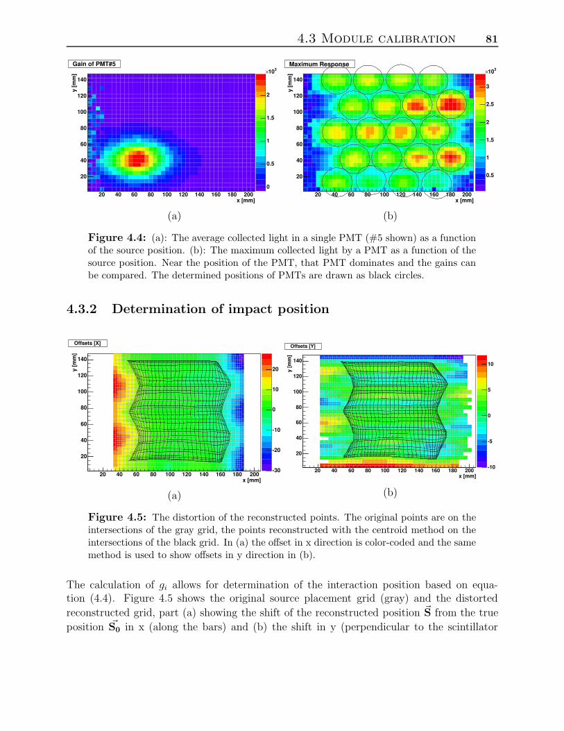
4.3 Module calibration 81
x [mm]20 40 60 80 100 120 140 160 180 200
y [m
m]
20
40
60
80
100
120
140
0
0.5
1
1.5
2
310×Gain of PMT#5
(a)
x [mm]20 40 60 80 100 120 140 160 180 200
y [m
m]
20
40
60
80
100
120
140
0.5
1
1.5
2
2.5
3
310×Maximum Response
(b)
Figure 4.4: (a): The average collected light in a single PMT (#5 shown) as a functionof the source position. (b): The maximum collected light by a PMT as a function of thesource position. Near the position of the PMT, that PMT dominates and the gains canbe compared. The determined positions of PMTs are drawn as black circles.
4.3.2 Determination of impact position
x [mm]20 40 60 80 100 120 140 160 180 200
y [m
m]
20
40
60
80
100
120
140
-30
-20
-10
0
10
20
Offsets [X]
(a)
x [mm]20 40 60 80 100 120 140 160 180 200
y [m
m]
20
40
60
80
100
120
140
-10
-5
0
5
10
Offsets [Y]
(b)
Figure 4.5: The distortion of the reconstructed points. The original points are on theintersections of the gray grid, the points reconstructed with the centroid method on theintersections of the black grid. In (a) the offset in x direction is color-coded and the samemethod is used to show offsets in y direction in (b).
The calculation of gi allows for determination of the interaction position based on equa-tion (4.4). Figure 4.5 shows the original source placement grid (gray) and the distorted
reconstructed grid, part (a) showing the shift of the reconstructed position ~S from the true
position ~S0 in x (along the bars) and (b) the shift in y (perpendicular to the scintillator
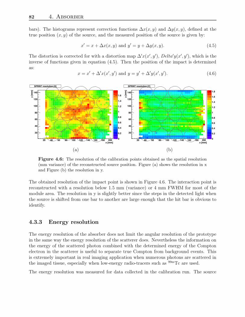
82 4. Absorber
bars). The histograms represent correction functions ∆x(x, y) and ∆y(x, y), defined at thetrue position (x, y) of the source, and the measured position of the source is given by:
x′ = x + ∆x(x, y) and y′ = y + ∆y(x, y). (4.5)
The distortion is corrected for with a distortion map ∆′x(x′, y′), Delta′y(x′, y′), which is theinverse of functions given in equation (4.5). Then the position of the impact is determinedas:
x = x′ + ∆′x(x′, y′) and y = y′ + ∆′y(x′, y′). (4.6)
x [mm]20 40 60 80 100 120 140 160 180 200
y [m
m]
20
40
60
80
100
120
140
0
0.2
0.4
0.6
0.8
1
1.2
1.4
1.6
SPRINT resolution [X]
(a)
x [mm]20 40 60 80 100 120 140 160 180 200
y [m
m]
20
40
60
80
100
120
140
0
0.2
0.4
0.6
0.8
1
1.2
1.4
1.6
1.8
SPRINT resolution [Y]
(b)
Figure 4.6: The resolution of the calibration points obtained as the spatial resolution(mm variance) of the reconstructed source position. Figure (a) shows the resolution in xand Figure (b) the resolution in y.
The obtained resolution of the impact point is shown in Figure 4.6. The interaction point isreconstructed with a resolution below 1.5 mm (variance) or 4 mm FWHM for most of themodule area. The resolution in y is slightly better since the steps in the detected light whenthe source is shifted from one bar to another are large enough that the hit bar is obvious toidentify.
4.3.3 Energy resolution
The energy resolution of the absorber does not limit the angular resolution of the prototypein the same way the energy resolution of the scatterer does. Nevertheless the information onthe energy of the scattered photon combined with the determined energy of the Comptonelectron in the scatterer is useful to separate true Compton from background events. Thisis extremely important in real imaging application when numerous photons are scattered inthe imaged tissue, especially when low-energy radio-tracers such as 99mTc are used.
The energy resolution was measured for data collected in the calibration run. The source
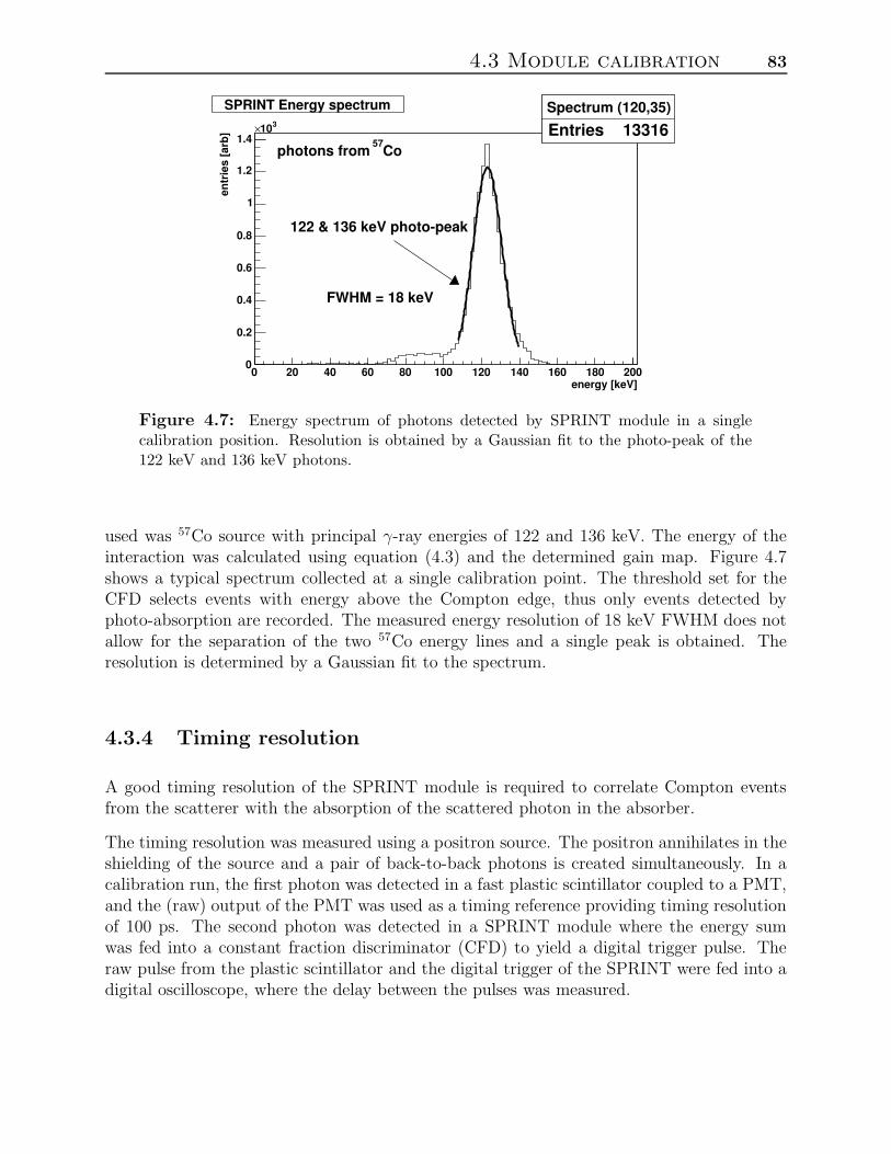
4.3 Module calibration 83
Spectrum (120,35)
Entries 13316
energy [keV]0 20 40 60 80 100 120 140 160 180 200
entr
ies
[arb
]
0
0.2
0.4
0.6
0.8
1
1.2
1.4310×
Spectrum (120,35)
Entries 13316SPRINT Energy spectrum
Co57photons from
122 & 136 keV photo-peak
FWHM = 18 keV
Figure 4.7: Energy spectrum of photons detected by SPRINT module in a singlecalibration position. Resolution is obtained by a Gaussian fit to the photo-peak of the122 keV and 136 keV photons.
used was 57Co source with principal γ-ray energies of 122 and 136 keV. The energy of theinteraction was calculated using equation (4.3) and the determined gain map. Figure 4.7shows a typical spectrum collected at a single calibration point. The threshold set for theCFD selects events with energy above the Compton edge, thus only events detected byphoto-absorption are recorded. The measured energy resolution of 18 keV FWHM does notallow for the separation of the two 57Co energy lines and a single peak is obtained. Theresolution is determined by a Gaussian fit to the spectrum.
4.3.4 Timing resolution
A good timing resolution of the SPRINT module is required to correlate Compton eventsfrom the scatterer with the absorption of the scattered photon in the absorber.
The timing resolution was measured using a positron source. The positron annihilates in theshielding of the source and a pair of back-to-back photons is created simultaneously. In acalibration run, the first photon was detected in a fast plastic scintillator coupled to a PMT,and the (raw) output of the PMT was used as a timing reference providing timing resolutionof 100 ps. The second photon was detected in a SPRINT module where the energy sumwas fed into a constant fraction discriminator (CFD) to yield a digital trigger pulse. Theraw pulse from the plastic scintillator and the digital trigger of the SPRINT were fed into adigital oscilloscope, where the delay between the pulses was measured.
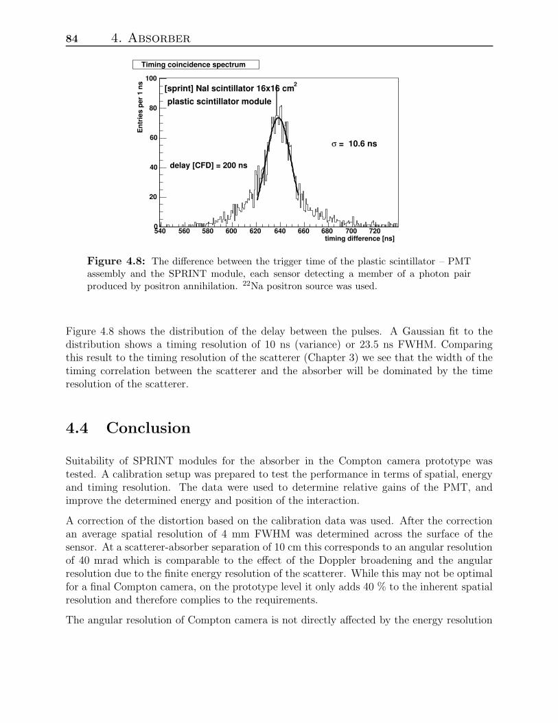
84 4. Absorber
timing difference [ns]540 560 580 600 620 640 660 680 700 720
Ent
ries
per
1 n
s
0
20
40
60
80
100
Timing coincidence spectrum
= 10.6 nsσ
2[sprint] NaI scintillator 16x16 cmplastic scintillator module
delay [CFD] = 200 ns
Figure 4.8: The difference between the trigger time of the plastic scintillator – PMTassembly and the SPRINT module, each sensor detecting a member of a photon pairproduced by positron annihilation. 22Na positron source was used.
Figure 4.8 shows the distribution of the delay between the pulses. A Gaussian fit to thedistribution shows a timing resolution of 10 ns (variance) or 23.5 ns FWHM. Comparingthis result to the timing resolution of the scatterer (Chapter 3) we see that the width of thetiming correlation between the scatterer and the absorber will be dominated by the timeresolution of the scatterer.
4.4 Conclusion
Suitability of SPRINT modules for the absorber in the Compton camera prototype wastested. A calibration setup was prepared to test the performance in terms of spatial, energyand timing resolution. The data were used to determine relative gains of the PMT, andimprove the determined energy and position of the interaction.
A correction of the distortion based on the calibration data was used. After the correctionan average spatial resolution of 4 mm FWHM was determined across the surface of thesensor. At a scatterer-absorber separation of 10 cm this corresponds to an angular resolutionof 40 mrad which is comparable to the effect of the Doppler broadening and the angularresolution due to the finite energy resolution of the scatterer. While this may not be optimalfor a final Compton camera, on the prototype level it only adds 40 % to the inherent spatialresolution and therefore complies to the requirements.
The angular resolution of Compton camera is not directly affected by the energy resolution

4.4 Conclusion 85
of the absorber, but the sum of energies recorded in the scatterer and the absorber is usefulto reject the background events. The energy resolution of the sum is dominated by theenergy resolution of the absorber which equals to 20 keV FWHM.
Timing resolution of the absorber is required for a proper matching of Compton scatterevents in the scatterer to the capture of the scattered photon in the absorber. The triggerof a SPRINT module is based on the energy sum of the shaped outputs of all 20 PMTsdiscriminated by a constant fraction discriminator (CFD). The timing resolution of thetrigger was measured to be 24 ns FWHM and the error on the timing correlation betweenthe scatterer and the absorber is dominated by the resolution of the scatterer.
Using SPRINT at higher energies of the photons significantly affects the efficiency of thesetup. At an energy of 140.5 keV the efficiency of the module with 1.27 cm thick NaI isclose to 100 % and drops to approximately 60% at 250 keV and to approximately 10 % for511 keV photons.

86 4. Absorber
Chapter 5
Compton camera prototype
A Compton camera prototype was constructed in order to verify the theoretical principlesand predictions for Compton camera performance. The prototype consists of two prototypeparts: the scatterer and the absorber. The implementation of the prototype combines triggersignals from both parts into a system trigger; data from both parts represent a Comptonscattering event. A set of scattering events is used by off-line software to reconstruct thesource position. Performance of the prototype is determined primarily by the quality ofdata, which is given by performance of individual parts. The timing correlation betweensub-detectors is also of great importance, because it provides interaction matching and data-sample purification. The timing correlation also determines the maximal source activity andamount of radio-active background, which can be tolerated in the setup. The last on thelist of performance parameters is the data throughput in terms of event rate, a requirementdirected towards read-out electronics rather than the core of the sensor operation.
The Compton camera prototype was constructed using the scatterer and absorber modulespresented in the preceding chapters. The reasons for selection of the specific sub-detectorswere given in the respective chapters. A simple geometry of the setup was chosen containingthree SPRINT modules forming an incomplete ring with the scatterer modules set on thering axis, following the arrangement suggested by previous Compton camera prototypes[LCH+98, MKW+93].
This chapter is devoted to the presentation of the prototype setup, both from mechanical andelectronic point of view. The geometrical layout of the modules determines the theoreticalproperties that depend on the prototype geometry, such as the setup efficiency and thegeometrical contribution to the error on spatial resolution of the source reconstruction. Theprocedure for the reconstruction of the source position is very complex and hence describedin a separate chapter.
87
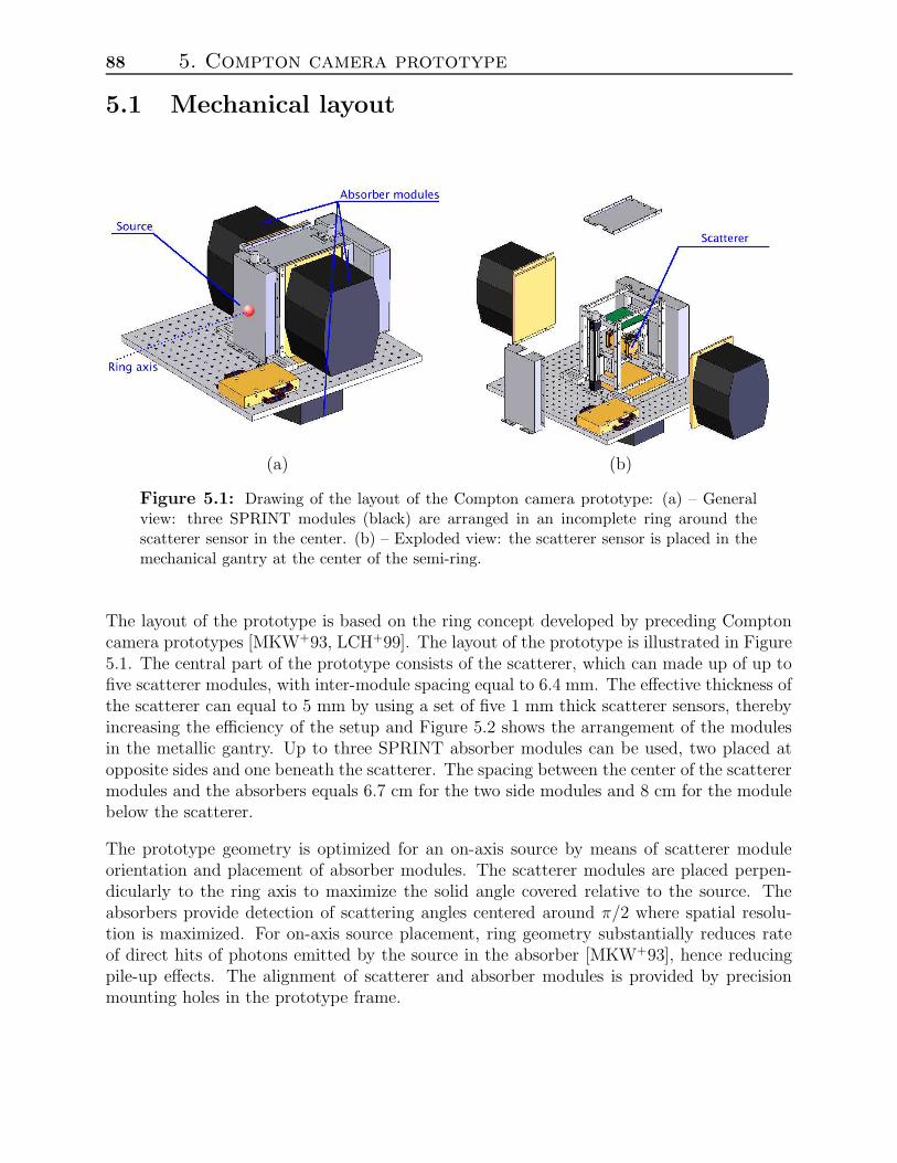
88 5. Compton camera prototype
5.1 Mechanical layout
(a) (b)
Figure 5.1: Drawing of the layout of the Compton camera prototype: (a) – Generalview: three SPRINT modules (black) are arranged in an incomplete ring around thescatterer sensor in the center. (b) – Exploded view: the scatterer sensor is placed in themechanical gantry at the center of the semi-ring.
The layout of the prototype is based on the ring concept developed by preceding Comptoncamera prototypes [MKW+93, LCH+99]. The layout of the prototype is illustrated in Figure5.1. The central part of the prototype consists of the scatterer, which can made up of up tofive scatterer modules, with inter-module spacing equal to 6.4 mm. The effective thickness ofthe scatterer can equal to 5 mm by using a set of five 1 mm thick scatterer sensors, therebyincreasing the efficiency of the setup and Figure 5.2 shows the arrangement of the modulesin the metallic gantry. Up to three SPRINT absorber modules can be used, two placed atopposite sides and one beneath the scatterer. The spacing between the center of the scatterermodules and the absorbers equals 6.7 cm for the two side modules and 8 cm for the modulebelow the scatterer.
The prototype geometry is optimized for an on-axis source by means of scatterer moduleorientation and placement of absorber modules. The scatterer modules are placed perpen-dicularly to the ring axis to maximize the solid angle covered relative to the source. Theabsorbers provide detection of scattering angles centered around π/2 where spatial resolu-tion is maximized. For on-axis source placement, ring geometry substantially reduces rateof direct hits of photons emitted by the source in the absorber [MKW+93], hence reducingpile-up effects. The alignment of scatterer and absorber modules is provided by precisionmounting holes in the prototype frame.
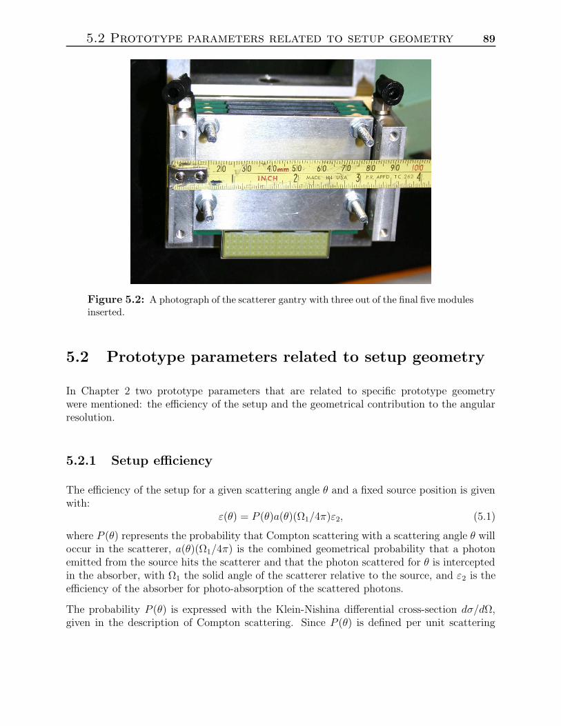
5.2 Prototype parameters related to setup geometry 89
Figure 5.2: A photograph of the scatterer gantry with three out of the final five modulesinserted.
5.2 Prototype parameters related to setup geometry
In Chapter 2 two prototype parameters that are related to specific prototype geometrywere mentioned: the efficiency of the setup and the geometrical contribution to the angularresolution.
5.2.1 Setup efficiency
The efficiency of the setup for a given scattering angle θ and a fixed source position is givenwith:
ε(θ) = P (θ)a(θ)(Ω1/4π)ε2, (5.1)
where P (θ) represents the probability that Compton scattering with a scattering angle θ willoccur in the scatterer, a(θ)(Ω1/4π) is the combined geometrical probability that a photonemitted from the source hits the scatterer and that the photon scattered for θ is interceptedin the absorber, with Ω1 the solid angle of the scatterer relative to the source, and ε2 is theefficiency of the absorber for photo-absorption of the scattered photons.
The probability P (θ) is expressed with the Klein-Nishina differential cross-section dσ/dΩ,given in the description of Compton scattering. Since P (θ) is defined per unit scattering
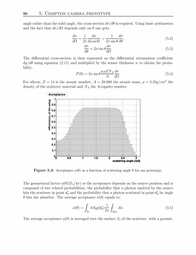
90 5. Compton camera prototype
angle rather than the solid angle, the cross-section dσ/dθ is required. Using basic arithmeticsand the fact that dσ/dΩ depends only on θ one gets:
dσ
dΩ=
1
2π
dσ
d(cos θ)=
1
2π sin θ
dσ
dθ, (5.2)
dσ
dθ= 2π sin θ
dσ
dΩ. (5.3)
The differential cross-section is then expressed as the differential attenuation coefficientdµ/dθ using equation (2.11) and multiplied by the sensor thickness w to obtain the proba-bility:
P (θ) = 2π sin θwρZNA
A
dσ
dΩ. (5.4)
For silicon, Z = 14 is the atomic number, A = 28.086 the atomic mass, ρ = 2.33g/cm3 thedensity of the scatterer material and NA the Avogadro number.
scattering angle [rad]0 0.5 1 1.5 2 2.5 3
scattering angle [rad]0 0.5 1 1.5 2 2.5 3
effic
icie
ncy
of th
e se
tup
0
0.1
0.2
0.3
0.4
0.5
0.6
0.7
0.8
0.9
1
Acceptance
Figure 5.3: Acceptance a(θ) as a function of scattering angle θ for our prototype.
The geometrical factor a(θ)(Ω1/4π) or the acceptance depends on the source position and iscomposed of two related probabilities: the probability that a photon emitted by the sourcehits the scatterer in point ~rs and the probability that a photon scattered in point ~rs by angleθ hits the absorber. The average acceptance a(θ) equals to:
a(θ) =
∫
Ss
d ~rsp(~rs)1
2π
∫
∆φa
dφ. (5.5)
The average acceptance a(θ) is averaged over the surface Ss of the scatterer, with a geomet-
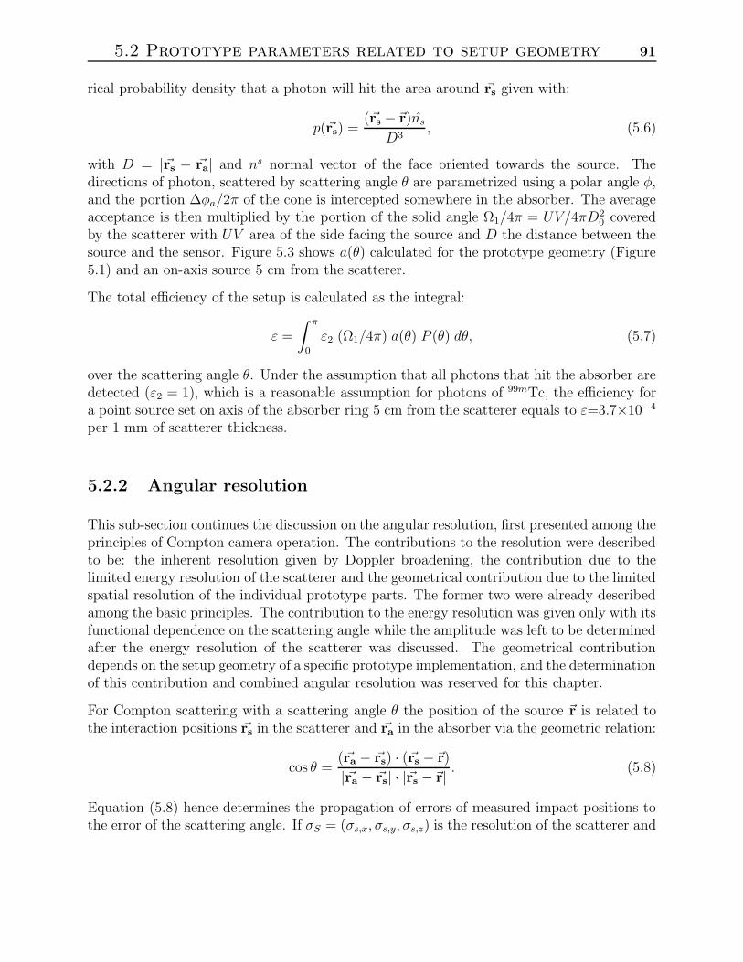
5.2 Prototype parameters related to setup geometry 91
rical probability density that a photon will hit the area around ~rs given with:
p(~rs) =(~rs −~r)ns
D3, (5.6)
with D = |~rs − ~ra| and ns normal vector of the face oriented towards the source. Thedirections of photon, scattered by scattering angle θ are parametrized using a polar angle φ,and the portion ∆φa/2π of the cone is intercepted somewhere in the absorber. The averageacceptance is then multiplied by the portion of the solid angle Ω1/4π = UV/4πD2
0 coveredby the scatterer with UV area of the side facing the source and D the distance between thesource and the sensor. Figure 5.3 shows a(θ) calculated for the prototype geometry (Figure5.1) and an on-axis source 5 cm from the scatterer.
The total efficiency of the setup is calculated as the integral:
ε =
∫ π
0
ε2 (Ω1/4π) a(θ) P (θ) dθ, (5.7)
over the scattering angle θ. Under the assumption that all photons that hit the absorber aredetected (ε2 = 1), which is a reasonable assumption for photons of 99mTc, the efficiency fora point source set on axis of the absorber ring 5 cm from the scatterer equals to ε=3.7×10⁻⁴
per 1 mm of scatterer thickness.
5.2.2 Angular resolution
This sub-section continues the discussion on the angular resolution, first presented among theprinciples of Compton camera operation. The contributions to the resolution were describedto be: the inherent resolution given by Doppler broadening, the contribution due to thelimited energy resolution of the scatterer and the geometrical contribution due to the limitedspatial resolution of the individual prototype parts. The former two were already describedamong the basic principles. The contribution to the energy resolution was given only with itsfunctional dependence on the scattering angle while the amplitude was left to be determinedafter the energy resolution of the scatterer was discussed. The geometrical contributiondepends on the setup geometry of a specific prototype implementation, and the determinationof this contribution and combined angular resolution was reserved for this chapter.
For Compton scattering with a scattering angle θ the position of the source ~r is related tothe interaction positions ~rs in the scatterer and ~ra in the absorber via the geometric relation:
cos θ =(~ra − ~rs) · (~rs −~r)
|~ra − ~rs| · |~rs −~r| . (5.8)
Equation (5.8) hence determines the propagation of errors of measured impact positions tothe error of the scattering angle. If σS = (σs,x, σs,y, σs,z) is the resolution of the scatterer and
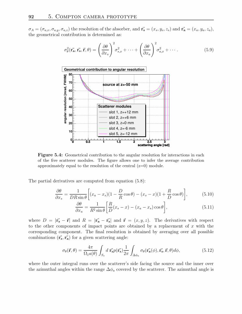
92 5. Compton camera prototype
σA = (σa,x, σa,y, σa,z) the resolution of the absorber, and ~rs = (xs, ys, zs) and ~ra = (xa, ya, za),the geometrical contribution is determined as:
σ2θ(~ra, ~rs,~r, θ) =
(
∂θ
∂xs
)2
σ2s,x + · · ·+
(
∂θ
∂xa
)2
σ2a,x + · · · . (5.9)
scattering angle [rad]0 0.5 1 1.5 2 2.5 3
scattering angle [rad]0 0.5 1 1.5 2 2.5 3
angu
lar
reso
lutio
n [m
rad,
FW
HM
]
0
10
20
30
40
50
60
70
80Geometrical contribution to angular resolution
Scatterer modulesslot 1, z=+12 mmslot 2, z=+6 mmslot 3, z=0 mmslot 4, z=-6 mmslot 5, z=-12 mm
source at z=-50 mm
Figure 5.4: Geometrical contribution to the angular resolution for interactions in eachof the five scatterer modules. The figure allows one to infer the average contributionapproximately equal to the resolution of the central (z=0) module.
The partial derivatives are computed from equation (5.8):
∂θ
∂xs=
1
DR sin θ
[
(xa − xs)(1 − D
Rcos θ) − (xs − x)(1 +
R
Dcos θ)
]
, (5.10)
∂θ
∂xa=
1
R2 sin θ
[
R
D(xs − x) − (xa − xs) cos θ
]
, (5.11)
where D = |~rs − ~r| and R = |~ra − ~rs| and ~r = (x, y, z). The derivatives with respectto the other components of impact points are obtained by a replacement of x with thecorresponding component. The final resolution is obtained by averaging over all possiblecombinations (~rs, ~ra) for a given scattering angle:
σθ(~r, θ) =4π
Ω1a(θ)
∫
Ss
d ~rsp(~rs)1
2π
∫
∆φa
σθ(~ra(φ), ~rs,~r, θ)dφ, (5.12)
where the outer integral runs over the scatterer’s side facing the source and the inner overthe azimuthal angles within the range ∆φa covered by the scatterer. The azimuthal angle is
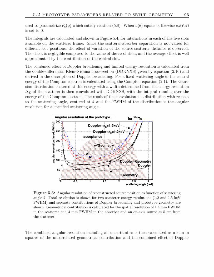
5.2 Prototype parameters related to setup geometry 93
used to parametrize ~ra(φ) which satisfy relation (5.8). When a(θ) equals 0, likewise σθ(~r, θ)is set to 0.
The integrals are calculated and shown in Figure 5.4, for interactions in each of the five slotsavailable on the scatterer frame. Since the scatterer-absorber separation is not varied fordifferent slot positions, the effect of variation of the source-scatterer distance is observed.The effect is negligible compared to the value of the resolution, and the average effect is wellapproximated by the contribution of the central slot.
The combined effect of Doppler broadening and limited energy resolution is calculated fromthe double-differential Klein-Nishina cross-section (DDKNXS) given by equation (2.10) andderived in the description of Doppler broadening. For a fixed scattering angle θ, the centralenergy of the Compton electron is calculated using the Compton equation (2.1). The Gaus-sian distribution centered at this energy with a width determined from the energy resolution∆E of the scatterer is then convoluted with DDKNXS, with the integral running over theenergy of the Compton electron. The result of the convolution is a distribution with respectto the scattering angle, centered at θ and the FWHM of the distribution is the angularresolution for a specified scattering angle.
scattering angle [rad]0 0.5 1 1.5 2 2.5 3
scattering angle [rad]0 0.5 1 1.5 2 2.5 3
angu
lar
reso
lutio
n [m
rad,
FW
HM
]
0
50
100
150
200
250
300
Doppler+GeometryDoppler
Geometry
w/Geometry
=1.5keVE∆Doppler+
=1.2keVE∆Doppler+acceptance
Tc99mfor Angular resolution of the prototype
Figure 5.5: Angular resolution of reconstructed source position as function of scatteringangle θ. Total resolution is shown for two scatterer energy resolutions (1.2 and 1.5 keVFWHM) and separate contributions of Doppler broadening and prototype geometry areshown. Geometrical contribution is calculated for the spatial resolution of 1.4 mm FWHMin the scatterer and 4 mm FWHM in the absorber and an on-axis source at 5 cm fromthe scatterer.
The combined angular resolution including all uncertainties is then calculated as a sum insquares of the uncorrelated geometrical contribution and the combined effect of Doppler
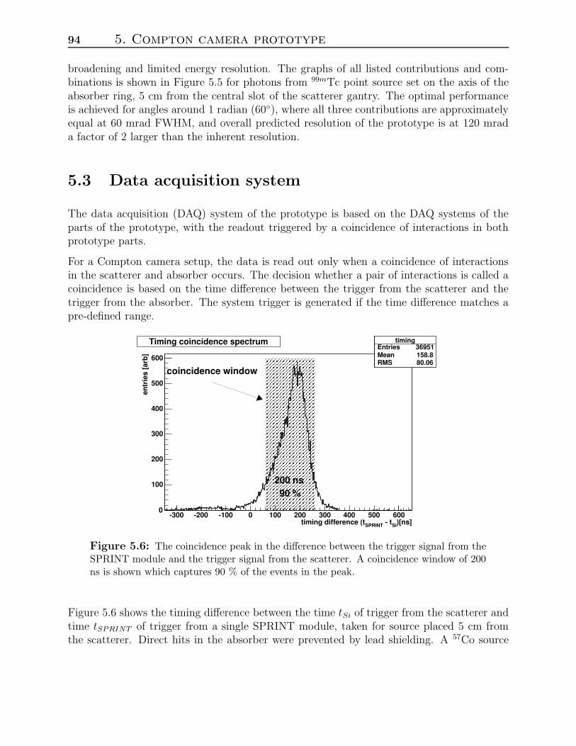
94 5. Compton camera prototype
broadening and limited energy resolution. The graphs of all listed contributions and com-binations is shown in Figure 5.5 for photons from 99mTc point source set on the axis of theabsorber ring, 5 cm from the central slot of the scatterer gantry. The optimal performanceis achieved for angles around 1 radian (60), where all three contributions are approximatelyequal at 60 mrad FWHM, and overall predicted resolution of the prototype is at 120 mrada factor of 2 larger than the inherent resolution.
5.3 Data acquisition system
The data acquisition (DAQ) system of the prototype is based on the DAQ systems of theparts of the prototype, with the readout triggered by a coincidence of interactions in bothprototype parts.
For a Compton camera setup, the data is read out only when a coincidence of interactionsin the scatterer and absorber occurs. The decision whether a pair of interactions is called acoincidence is based on the time difference between the trigger from the scatterer and thetrigger from the absorber. The system trigger is generated if the time difference matches apre-defined range.
timingEntries 36951Mean 158.8RMS 80.06
)[ns]Si - tSPRINTtiming difference (t-300 -200 -100 0 100 200 300 400 500 600
entr
ies
[arb
]
0
100
200
300
400
500
600
timingEntries 36951Mean 158.8RMS 80.06
Timing coincidence spectrum timingEntries 36951Mean 158.8RMS 80.06
90 %200 ns
coincidence window
Figure 5.6: The coincidence peak in the difference between the trigger signal from theSPRINT module and the trigger signal from the scatterer. A coincidence window of 200ns is shown which captures 90 % of the events in the peak.
Figure 5.6 shows the timing difference between the time tSi of trigger from the scatterer andtime tSPRINT of trigger from a single SPRINT module, taken for source placed 5 cm fromthe scatterer. Direct hits in the absorber were prevented by lead shielding. A 57Co source
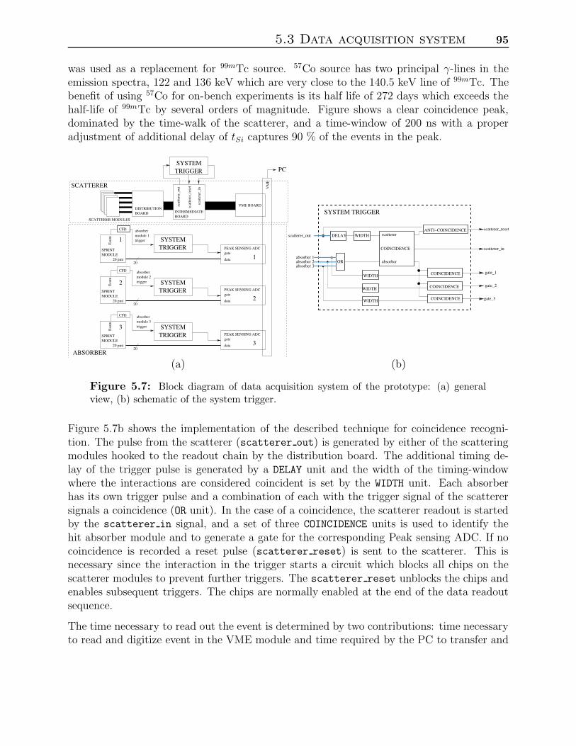
5.3 Data acquisition system 95
was used as a replacement for 99mTc source. 57Co source has two principal γ-lines in theemission spectra, 122 and 136 keV which are very close to the 140.5 keV line of 99mTc. Thebenefit of using 57Co for on-bench experiments is its half life of 272 days which exceeds thehalf-life of 99mTc by several orders of magnitude. Figure shows a clear coincidence peak,dominated by the time-walk of the scatterer, and a time-window of 200 ns with a properadjustment of additional delay of tSi captures 90 % of the events in the peak.
VME BOARD
VM
E
data
gatePEAK SENSING ADC
3MODULESPRINT
CFD
Esu
m
20 pmt20
data
gatePEAK SENSING ADC
2MODULESPRINT
CFD
Esu
m
20 pmt20
data
gatePEAK SENSING ADC
1MODULESPRINT
CFD
Esu
m
20 pmt20
3
2
1
PC
SCATTERER
ABSORBER
SYSTEMTRIGGER
SYSTEMTRIGGER
trigger
absorbermodule 1
SYSTEMtriggermodule 2absorber
TRIGGERtriggermodule 3absorber
TRIGGER
SYSTEM
DISTRIBUTIONBOARD
SCATTERER MODULES
INTERMEDIATEBOARD
scat
tere
r_ou
t
scat
tere
r_in
scat
tere
r_re
set
OR
H HI IJ JK KL LM M
scatterer_out
absorber 3absorber 2absorber 1
scatterer
absorber
ANTI−COINCIDENCE
SYSTEM TRIGGER
scatterer_reset
gate_1
gate_3
gate_2
scatterer_in
WIDTH
DELAY WIDTH
COINCIDENCE
WIDTH
WIDTH COINCIDENCE
COINCIDENCE
COINCIDENCE
(a) (b)
Figure 5.7: Block diagram of data acquisition system of the prototype: (a) generalview, (b) schematic of the system trigger.
Figure 5.7b shows the implementation of the described technique for coincidence recogni-tion. The pulse from the scatterer (scatterer out) is generated by either of the scatteringmodules hooked to the readout chain by the distribution board. The additional timing de-lay of the trigger pulse is generated by a DELAY unit and the width of the timing-windowwhere the interactions are considered coincident is set by the WIDTH unit. Each absorberhas its own trigger pulse and a combination of each with the trigger signal of the scatterersignals a coincidence (OR unit). In the case of a coincidence, the scatterer readout is startedby the scatterer in signal, and a set of three COINCIDENCE units is used to identify thehit absorber module and to generate a gate for the corresponding Peak sensing ADC. If nocoincidence is recorded a reset pulse (scatterer reset) is sent to the scatterer. This isnecessary since the interaction in the trigger starts a circuit which blocks all chips on thescatterer modules to prevent further triggers. The scatterer reset unblocks the chips andenables subsequent triggers. The chips are normally enabled at the end of the data readoutsequence.
The time necessary to read out the event is determined by two contributions: time necessaryto read and digitize event in the VME module and time required by the PC to transfer and
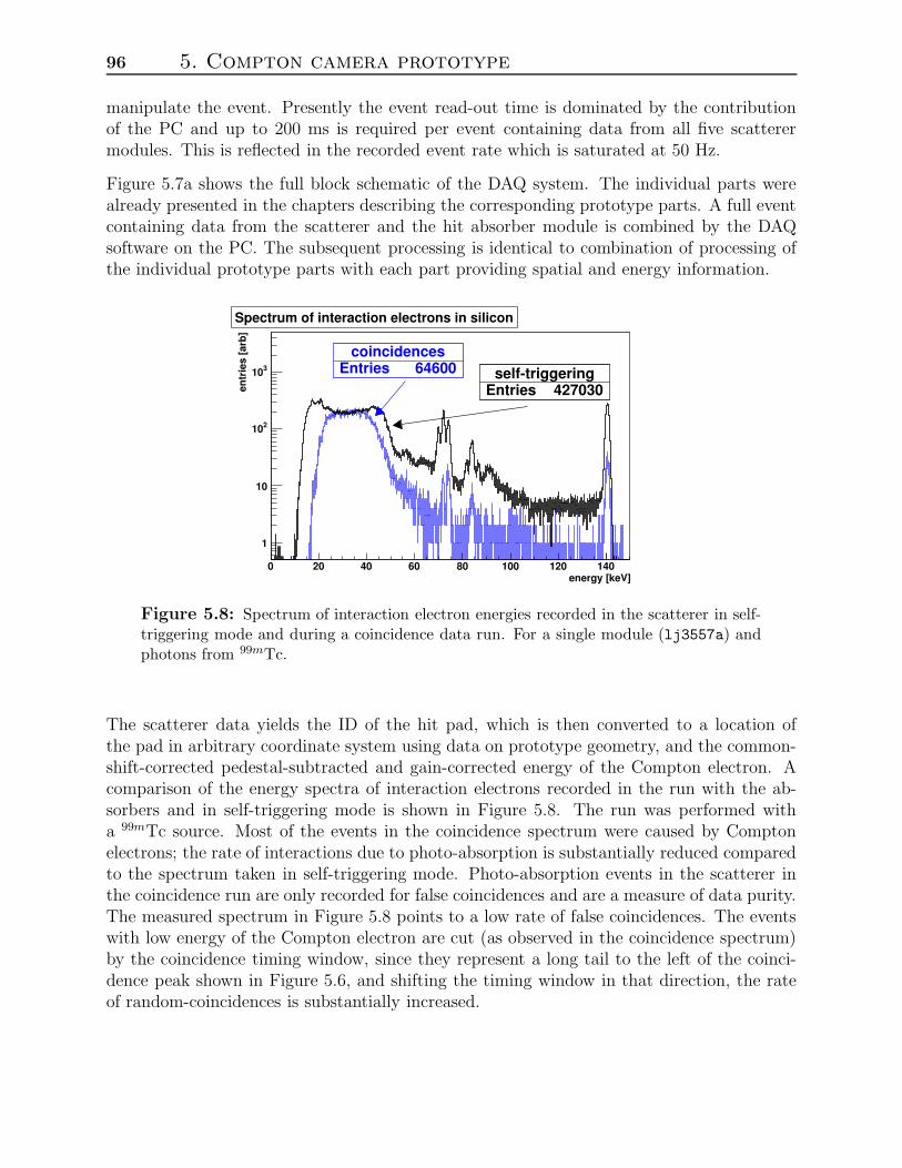
96 5. Compton camera prototype
manipulate the event. Presently the event read-out time is dominated by the contributionof the PC and up to 200 ms is required per event containing data from all five scatterermodules. This is reflected in the recorded event rate which is saturated at 50 Hz.
Figure 5.7a shows the full block schematic of the DAQ system. The individual parts werealready presented in the chapters describing the corresponding prototype parts. A full eventcontaining data from the scatterer and the hit absorber module is combined by the DAQsoftware on the PC. The subsequent processing is identical to combination of processing ofthe individual prototype parts with each part providing spatial and energy information.
coincidencesEntries 64600
energy [keV]0 20 40 60 80 100 120 140
entr
ies
[arb
]
1
10
210
310
coincidencesEntries 64600
Spectrum of interaction electrons in silicon
self-triggeringEntries 427030
self-triggeringEntries 427030
self-triggeringEntries 427030
Figure 5.8: Spectrum of interaction electron energies recorded in the scatterer in self-triggering mode and during a coincidence data run. For a single module (lj3557a) andphotons from 99mTc.
The scatterer data yields the ID of the hit pad, which is then converted to a location ofthe pad in arbitrary coordinate system using data on prototype geometry, and the common-shift-corrected pedestal-subtracted and gain-corrected energy of the Compton electron. Acomparison of the energy spectra of interaction electrons recorded in the run with the ab-sorbers and in self-triggering mode is shown in Figure 5.8. The run was performed witha 99mTc source. Most of the events in the coincidence spectrum were caused by Comptonelectrons; the rate of interactions due to photo-absorption is substantially reduced comparedto the spectrum taken in self-triggering mode. Photo-absorption events in the scatterer inthe coincidence run are only recorded for false coincidences and are a measure of data purity.The measured spectrum in Figure 5.8 points to a low rate of false coincidences. The eventswith low energy of the Compton electron are cut (as observed in the coincidence spectrum)by the coincidence timing window, since they represent a long tail to the left of the coinci-dence peak shown in Figure 5.6, and shifting the timing window in that direction, the rateof random-coincidences is substantially increased.
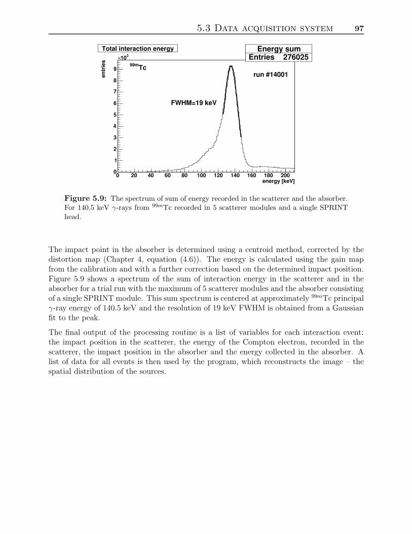
5.3 Data acquisition system 97
Energy sumEntries 276025
energy [keV]0 20 40 60 80 100 120 140 160 180 200
entr
ies
0
1
2
3
4
5
6
7
8
9
310×Energy sum
Entries 276025Total interaction energy
FWHM=19 keV
run #14001Tc99m
Figure 5.9: The spectrum of sum of energy recorded in the scatterer and the absorber.For 140.5 keV γ-rays from 99mTc recorded in 5 scatterer modules and a single SPRINThead.
The impact point in the absorber is determined using a centroid method, corrected by thedistortion map (Chapter 4, equation (4.6)). The energy is calculated using the gain mapfrom the calibration and with a further correction based on the determined impact position.Figure 5.9 shows a spectrum of the sum of interaction energy in the scatterer and in theabsorber for a trial run with the maximum of 5 scatterer modules and the absorber consistingof a single SPRINT module. This sum spectrum is centered at approximately 99mTc principalγ-ray energy of 140.5 keV and the resolution of 19 keV FWHM is obtained from a Gaussianfit to the peak.
The final output of the processing routine is a list of variables for each interaction event:the impact position in the scatterer, the energy of the Compton electron, recorded in thescatterer, the impact position in the absorber and the energy collected in the absorber. Alist of data for all events is then used by the program, which reconstructs the image – thespatial distribution of the sources.

98 5. Compton camera prototype
Chapter 6
Image reconstruction
The Compton camera is an imaging device, and a vital part of data analysis is the imagereconstruction. The task of the reconstruction algorithm is to determine the distribution ofradioactive sources based on collected data. The input to the reconstruction algorithm isa list of events, with each event containing impact positions in both parts of the prototypeand the respective recorded energies. The output is a three-dimensional histogram filledwith probabilities that the source is present in a certain voxel–bin of the histogram.
The intention of the image reconstruction was the evaluation of the prototype, hence asimple back-projection was used. When a more precise source distribution is sought, thereare a few more refined methods available. They can be split into analytical and approximatereconstruction methods, and an approximate method suitable for our application, calledexpectation maximization list-mode maximum likelihood is described in Appendix B.
6.1 Definition of problem
The imaging problem is posed as follows: the distribution of sources is given with a (scalar)field S(~r) or an image, which describes the relative intensity (concentration) of the radionu-clide at a point ~r in real space, the space also referred to as the source space. The photonsemitted by the sources are detected in the detector and each event consists of measurement ofseveral parameters. For a Compton camera, those are the interaction position ~rs and energyEs recorded in the scatterer and the hit position ~ra in the absorber1, and an 7-dimensionalvector y = (~rs, Es, ~ra) representing a possible scattering realization is formed. The basicprinciples of Compton camera and the information on the geometry of the setup are used to
1The energy Ea recorded in the absorber is used only for rejection of background events and is not a partof image reconstruction data
99
100 6. Image reconstruction
determine the probability:f(y|S(~r)), (6.1)
that a realization y is measured given a source distribution S(~r). The vectors y span themeasurement space and using the probability f() a scalar field (image) M(y) is formed as:
M(y) = f(y|S(~r)), (6.2)
with values of M() varying between 0 and 1. M(y) is viewed as a representation of the spatialdistribution S(~r) in the measurement space. Also, equation (6.2) shows how a measurementimage M(y) is constructed from the given spatial distribution and the inverse - obtainingthe source distribution from the measurement image - is called the image reconstruction.
Since the imaging system is linear, equation (6.2) can also be written in a matrix form,providing the measurements M() and the source distribution S() are discreticized. Themeasurement space is binned along all directions, i.e. the energy and position measured ineach part of the prototype, and a single index is used to denote a bin in this multi-dimensionalhistogram. A similar procedure is done on the source space, where a single index is used toidentify a position within the source distribution. The number of measurements mj in eachbin of the measurement space grows linearly with Ne, the number of detected events, andthe approximation to the measurement image as defined above is obtained by division of mj
with Ne: M() → mj/Ne. The source distribution is given with S() → si and along with mj
they are viewed as vectors, related by the system transfer matrix T :
mj =
N∑
i=1
T ji si, (6.3)
with N the number of bins used to discreticize the source space. The matrix elements Tji
are obtained as:
T ji = Ne
∫
Wj
d ~yj f(~y|Si), (6.4)
where Wj is the (hyper-) volume of bin j in the measurement space, ~yj the central measure-ment vector of bin j and Si a source distribution with a single source with unit intensityplaced at ~ri, the center ob bin i.
The finite Ne of measurements allow for formation of an approximate image M ′(y) and thereare two distinct approaches to obtaining the source distribution S(~r): an analytic and anapproximate reconstruction.
The analytic reconstruction inverts T directly, and based on the measurement collection m′j
the related source intensities si are obtained:
si =
M∑
j=0
T−1ij m′
j, (6.5)
6.1 Definition of problem 101
with M the number of bins used to discreticize the measurement space. There are severalcomplications involved in using the analytical approach: the errors of the data set m′
j, itsincompleteness and a large amount of computer power required for storage and manipulationof the transfer matrix. The effect of the measurement errors on the obtained image can bequite large, since the transfer matrix T tends to be ill-conditioned. This was observed byParra [Par00] and an adequate solution was proposed. The solution, however, requires a fullset of measurement data to be known, i.e. all range of scattering angles. The problems relatedwith obtaining a full set of measurements (threshold in the scatterer, solid angle covered bythe absorber) combined with the fact that measurements will always contain errors remaina draw-back of the analytical method. New methods are proposed [TH03], which give ananalytical solution even on a limited data set with measurements errors. However, evenwith this problems solved, harsh requirements related to the computational power remain.Analytical methods require the storage and manipulation of the transfer matrix T , which isof dimension M × N . For example - the prototype consists of NS = 103 scatterer channels,NA = 104 absorber channels and the energy of the scatterer is binned in NE = 103 bins,which gives M = 1010. Let’s consider a cubic source grid with a lattice of 3 cm and a binof 1 mm3, or N=3×10⁴. An analytical reconstruction would require manipulation of matrixwith 3×10¹⁴ of entries, and assuming 4 bytes per bin, manipulation of PByte of data isrequired, which is practically impossible.
Approximate methods can operate without the complete knowledge of Tjk and are hence lessdemanding on the computing system. Because of that they were the reconstruction methodsof most of the so-far constructed prototypes. A maximum likelihood approach was developedby Herbert and Singh [HLS90], and Wilderman derived an expectation maximization algo-rithm for maximum likelihood on list-mode data [WFC+01] in 1998. The common approachof approximate methods is the following: assume a Poison distribution of mj number of en-
tries in each bin j of the measurement space, determine the average content m′j =
∑Ni=1 T jisi
for the sought source distribution si, and use maximum likelihood to determine unbiased es-timators for s′i. Since maximum likelihood produces a set of N coupled equations for s′i,the solution is sought iteratively, and an approximate solution is reached. The measurementerrors are included in the system matrix elements T ji and incompleteness of the data set istaken into account by evaluating m′
j only for a limited volume of measurement space; forlist-mode only bins containing measurements are taken. Expectation maximization list-modemaximum likelihood as given by [WFC+01] is described in Appendix B as an example of anapproximate reconstruction method.
There are some remaining problems of Compton camera image reconstruction, which are notsolved by any of the listed methods. For example, the image is reconstructed in a limitedspace, and a 0 probability is assumed for points lying outside of the reconstructed region. Forextended objects this causes edge artifacts, which can be only removed by careful modelingof expected tissue uptake [Zha04] prior to measurement. Even so, the noise of those eventsremains in the reconstructed image.
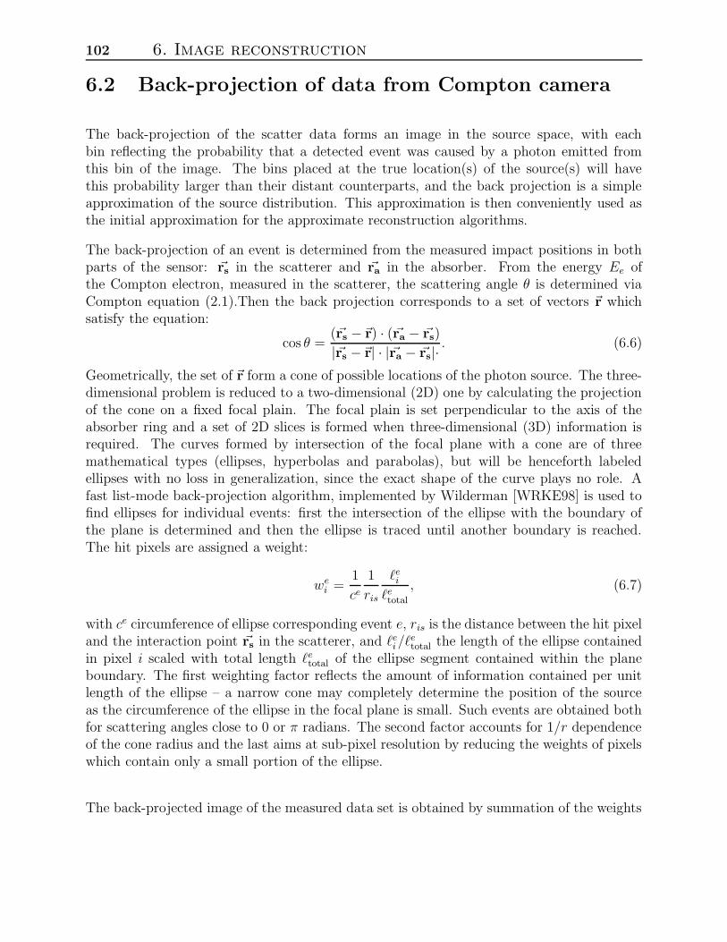
102 6. Image reconstruction
6.2 Back-projection of data from Compton camera
The back-projection of the scatter data forms an image in the source space, with eachbin reflecting the probability that a detected event was caused by a photon emitted fromthis bin of the image. The bins placed at the true location(s) of the source(s) will havethis probability larger than their distant counterparts, and the back projection is a simpleapproximation of the source distribution. This approximation is then conveniently used asthe initial approximation for the approximate reconstruction algorithms.
The back-projection of an event is determined from the measured impact positions in bothparts of the sensor: ~rs in the scatterer and ~ra in the absorber. From the energy Ee ofthe Compton electron, measured in the scatterer, the scattering angle θ is determined viaCompton equation (2.1).Then the back projection corresponds to a set of vectors ~r whichsatisfy the equation:
cos θ =(~rs −~r) · (~ra − ~rs)
|~rs −~r| · |~ra − ~rs|·. (6.6)
Geometrically, the set of ~r form a cone of possible locations of the photon source. The three-dimensional problem is reduced to a two-dimensional (2D) one by calculating the projectionof the cone on a fixed focal plain. The focal plain is set perpendicular to the axis of theabsorber ring and a set of 2D slices is formed when three-dimensional (3D) information isrequired. The curves formed by intersection of the focal plane with a cone are of threemathematical types (ellipses, hyperbolas and parabolas), but will be henceforth labeledellipses with no loss in generalization, since the exact shape of the curve plays no role. Afast list-mode back-projection algorithm, implemented by Wilderman [WRKE98] is used tofind ellipses for individual events: first the intersection of the ellipse with the boundary ofthe plane is determined and then the ellipse is traced until another boundary is reached.The hit pixels are assigned a weight:
wei =
1
ce
1
ris
`ei
`etotal
, (6.7)
with ce circumference of ellipse corresponding event e, ris is the distance between the hit pixeland the interaction point ~rs in the scatterer, and `e
i/`etotal the length of the ellipse contained
in pixel i scaled with total length `etotal of the ellipse segment contained within the plane
boundary. The first weighting factor reflects the amount of information contained per unitlength of the ellipse – a narrow cone may completely determine the position of the sourceas the circumference of the ellipse in the focal plane is small. Such events are obtained bothfor scattering angles close to 0 or π radians. The second factor accounts for 1/r dependenceof the cone radius and the last aims at sub-pixel resolution by reducing the weights of pixelswhich contain only a small portion of the ellipse.
The back-projected image of the measured data set is obtained by summation of the weights
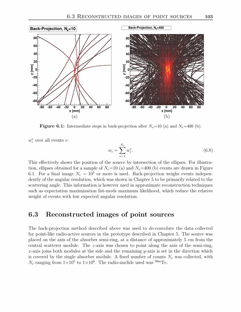
6.3 Reconstructed images of point sources 103
x [mm]-80 -60 -40 -20 0 20 40 60 80
y [m
m]
-80
-60
-40
-20
0
20
40
60
80
=10eBack-Projection, N
x [mm]-80 -60 -40 -20 0 20 40 60 80
y [m
m]
-80
-60
-40
-20
0
20
40
60
80
=400eBack-Projection, N
(a) (b)
Figure 6.1: Intermediate steps in back-projection after Ne=10 (a) and Ne=400 (b).
wei over all events e:
wi =
Ne∑
e=1
wei . (6.8)
This effectively shows the position of the source by intersection of the ellipses. For illustra-tion, ellipses obtained for a sample of Ne=10 (a) and Ne=400 (b) events are drawn in Figure6.1. For a final image Ne = 105 or more is used. Back-projection weighs events indepen-dently of the angular resolution, which was shown in Chapter 5 to be primarily related to thescattering angle. This information is however used in approximate reconstruction techniquessuch as expectation maximization list-mode maximum likelihood, which reduce the relativeweight of events with low expected angular resolution.
6.3 Reconstructed images of point sources
The back-projection method described above was used to de-convolute the data collectedfor point-like radio-active sources in the prototype described in Chapter 5. The source wasplaced on the axis of the absorber semi-ring, at a distance of approximately 5 cm from thecentral scatterer module. The z-axis was chosen to point along the axis of the semi-ring,x-axis joins both modules at the side and the remaining y-axis is set in the direction whichis covered by the single absorber module. A fixed number of counts Ne was collected, withNe ranging from 1×10⁵ to 1×10⁶. The radio-nuclide used was 99mTc.
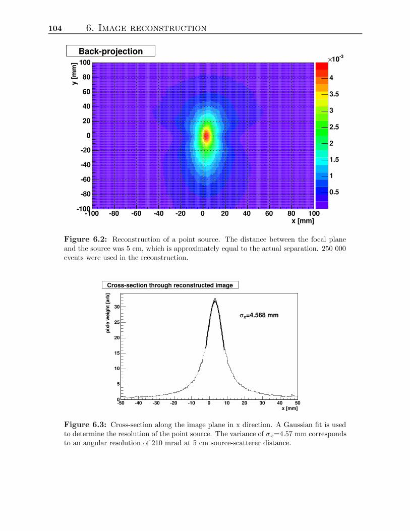
104 6. Image reconstruction
x [mm]-100 -80 -60 -40 -20 0 20 40 60 80 100
y [m
m]
-100
-80
-60
-40
-20
0
20
40
60
80
100
0.5
1
1.5
2
2.5
3
3.5
4
-310×Back-projection
Figure 6.2: Reconstruction of a point source. The distance between the focal planeand the source was 5 cm, which is approximately equal to the actual separation. 250 000events were used in the reconstruction.
x [mm]-50 -40 -30 -20 -10 0 10 20 30 40 50
pixl
e w
eigh
t [ar
b]
0
5
10
15
20
25
30
Cross-section through reconstructed image
=4.568 mmxσ
Figure 6.3: Cross-section along the image plane in x direction. A Gaussian fit is usedto determine the resolution of the point source. The variance of σx=4.57 mm correspondsto an angular resolution of 210 mrad at 5 cm source-scatterer distance.
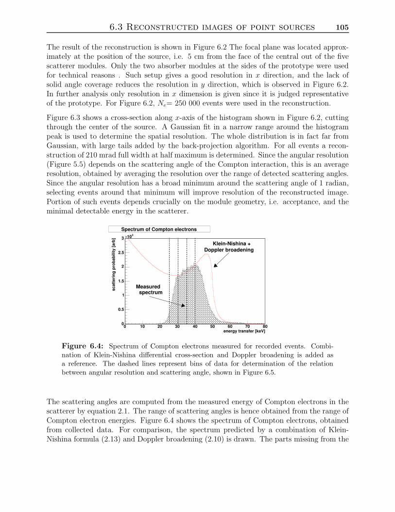
6.3 Reconstructed images of point sources 105
The result of the reconstruction is shown in Figure 6.2 The focal plane was located approx-imately at the position of the source, i.e. 5 cm from the face of the central out of the fivescatterer modules. Only the two absorber modules at the sides of the prototype were usedfor technical reasons . Such setup gives a good resolution in x direction, and the lack ofsolid angle coverage reduces the resolution in y direction, which is observed in Figure 6.2.In further analysis only resolution in x dimension is given since it is judged representativeof the prototype. For Figure 6.2, Ne= 250 000 events were used in the reconstruction.
Figure 6.3 shows a cross-section along x-axis of the histogram shown in Figure 6.2, cuttingthrough the center of the source. A Gaussian fit in a narrow range around the histogrampeak is used to determine the spatial resolution. The whole distribution is in fact far fromGaussian, with large tails added by the back-projection algorithm. For all events a recon-struction of 210 mrad full width at half maximum is determined. Since the angular resolution(Figure 5.5) depends on the scattering angle of the Compton interaction, this is an averageresolution, obtained by averaging the resolution over the range of detected scattering angles.Since the angular resolution has a broad minimum around the scattering angle of 1 radian,selecting events around that minimum will improve resolution of the reconstructed image.Portion of such events depends crucially on the module geometry, i.e. acceptance, and theminimal detectable energy in the scatterer.
energy transfer [keV]0 10 20 30 40 50 60 70 80
scat
teri
ng p
roba
bilit
y [a
rb]
0
0.5
1
1.5
2
2.5
3310×
Spectrum of Compton electrons
Klein-Nishina +Doppler broadening
Measuredspectrum
Figure 6.4: Spectrum of Compton electrons measured for recorded events. Combi-nation of Klein-Nishina differential cross-section and Doppler broadening is added asa reference. The dashed lines represent bins of data for determination of the relationbetween angular resolution and scattering angle, shown in Figure 6.5.
The scattering angles are computed from the measured energy of Compton electrons in thescatterer by equation 2.1. The range of scattering angles is hence obtained from the range ofCompton electron energies. Figure 6.4 shows the spectrum of Compton electrons, obtainedfrom collected data. For comparison, the spectrum predicted by a combination of Klein-Nishina formula (2.13) and Doppler broadening (2.10) is drawn. The parts missing from the
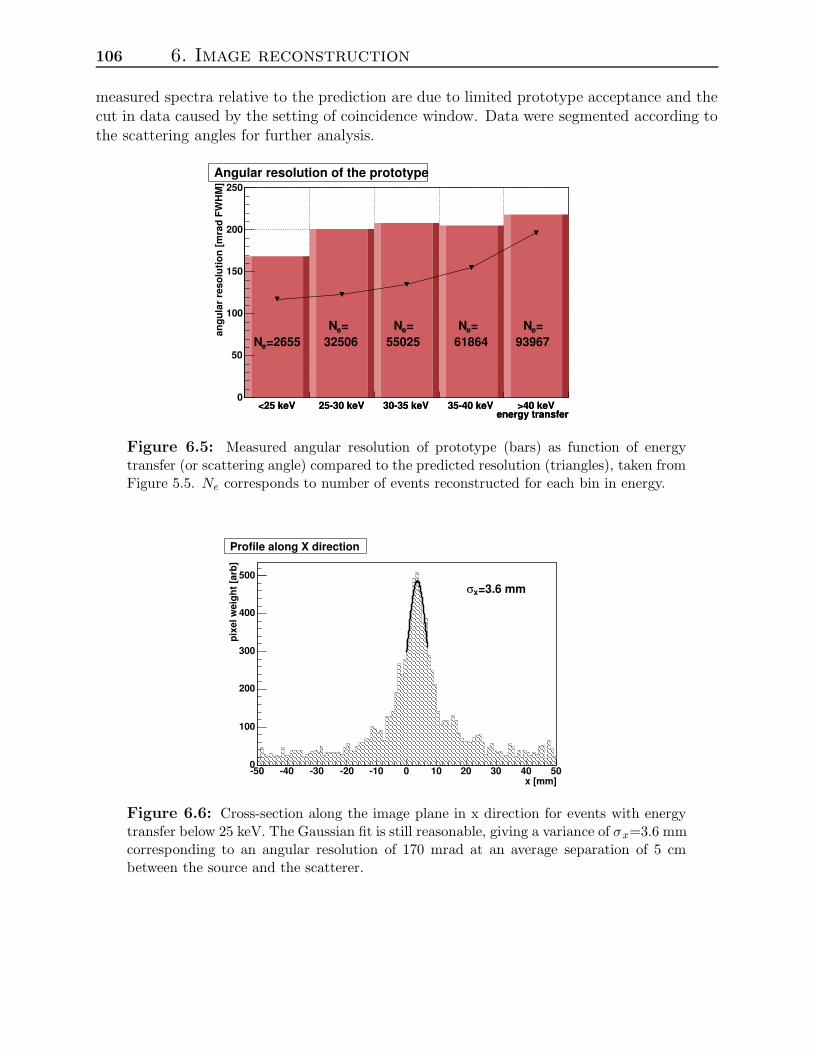
106 6. Image reconstruction
measured spectra relative to the prediction are due to limited prototype acceptance and thecut in data caused by the setting of coincidence window. Data were segmented according tothe scattering angles for further analysis.
energy transfer<25 keV 25-30 keV 30-35 keV 35-40 keV >40 keV
energy transfer<25 keV 25-30 keV 30-35 keV 35-40 keV >40 keV
angu
lar
reso
lutio
n [m
rad
FWH
M]
0
50
100
150
200
250Angular resolution of the prototype
=2655eN=eN
55025=eN
61864=eN
9396732506=eN
Figure 6.5: Measured angular resolution of prototype (bars) as function of energytransfer (or scattering angle) compared to the predicted resolution (triangles), taken fromFigure 5.5. Ne corresponds to number of events reconstructed for each bin in energy.
x [mm]-50 -40 -30 -20 -10 0 10 20 30 40 50
pixe
l wei
ght [
arb]
0
100
200
300
400
500
Profile along X direction
=3.6 mmxσ
Figure 6.6: Cross-section along the image plane in x direction for events with energytransfer below 25 keV. The Gaussian fit is still reasonable, giving a variance of σx=3.6 mmcorresponding to an angular resolution of 170 mrad at an average separation of 5 cmbetween the source and the scatterer.
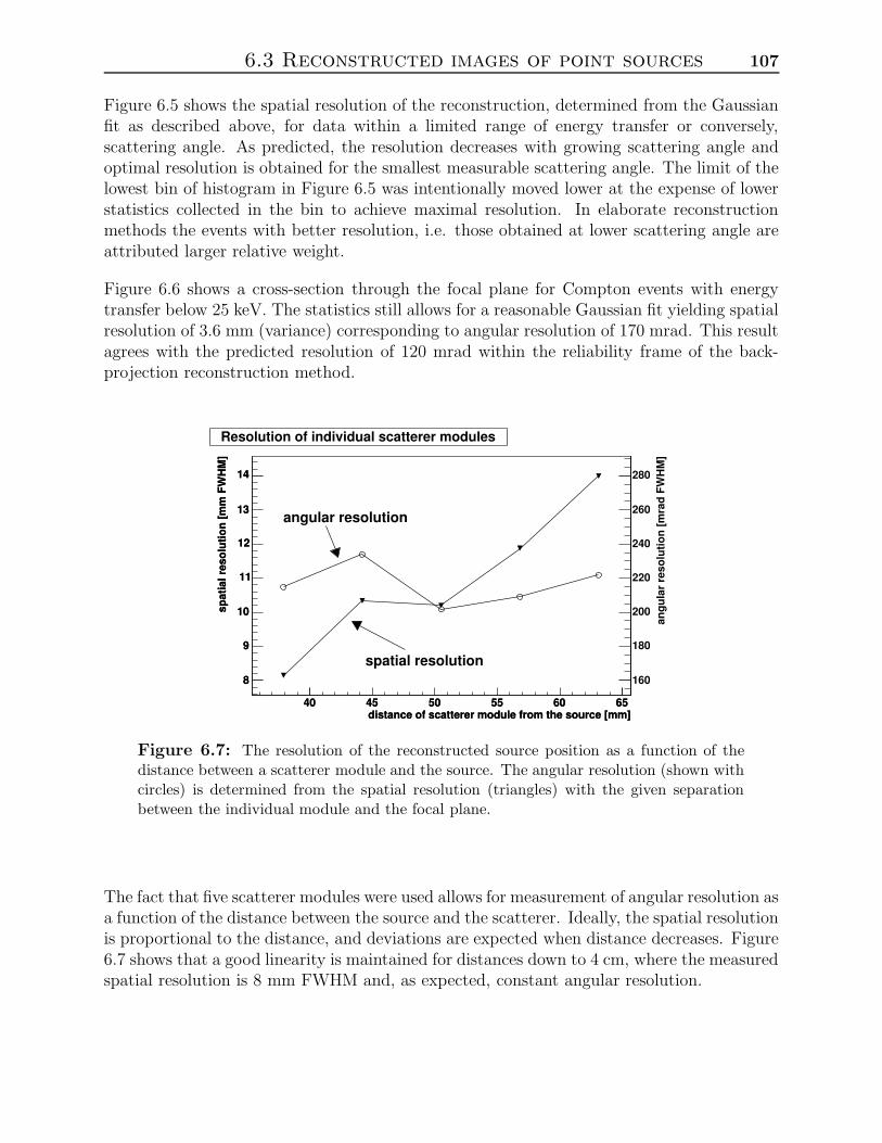
6.3 Reconstructed images of point sources 107
Figure 6.5 shows the spatial resolution of the reconstruction, determined from the Gaussianfit as described above, for data within a limited range of energy transfer or conversely,scattering angle. As predicted, the resolution decreases with growing scattering angle andoptimal resolution is obtained for the smallest measurable scattering angle. The limit of thelowest bin of histogram in Figure 6.5 was intentionally moved lower at the expense of lowerstatistics collected in the bin to achieve maximal resolution. In elaborate reconstructionmethods the events with better resolution, i.e. those obtained at lower scattering angle areattributed larger relative weight.
Figure 6.6 shows a cross-section through the focal plane for Compton events with energytransfer below 25 keV. The statistics still allows for a reasonable Gaussian fit yielding spatialresolution of 3.6 mm (variance) corresponding to angular resolution of 170 mrad. This resultagrees with the predicted resolution of 120 mrad within the reliability frame of the back-projection reconstruction method.
distance of scatterer module from the source [mm]40 45 50 55 60 65
spat
ial r
esol
utio
n [m
m F
WH
M]
8
9
10
11
12
13
14
Resolution of individual scatterer modules
distance of scatterer module from the source [mm]40 45 50 55 60 65
spat
ial r
esol
utio
n [m
m F
WH
M]
8
9
10
11
12
13
14
angu
lar
reso
lutio
n [m
rad
FWH
M]
160
180
200
220
240
260
280
spatial resolution
angular resolution
Figure 6.7: The resolution of the reconstructed source position as a function of thedistance between a scatterer module and the source. The angular resolution (shown withcircles) is determined from the spatial resolution (triangles) with the given separationbetween the individual module and the focal plane.
The fact that five scatterer modules were used allows for measurement of angular resolution asa function of the distance between the source and the scatterer. Ideally, the spatial resolutionis proportional to the distance, and deviations are expected when distance decreases. Figure6.7 shows that a good linearity is maintained for distances down to 4 cm, where the measuredspatial resolution is 8 mm FWHM and, as expected, constant angular resolution.
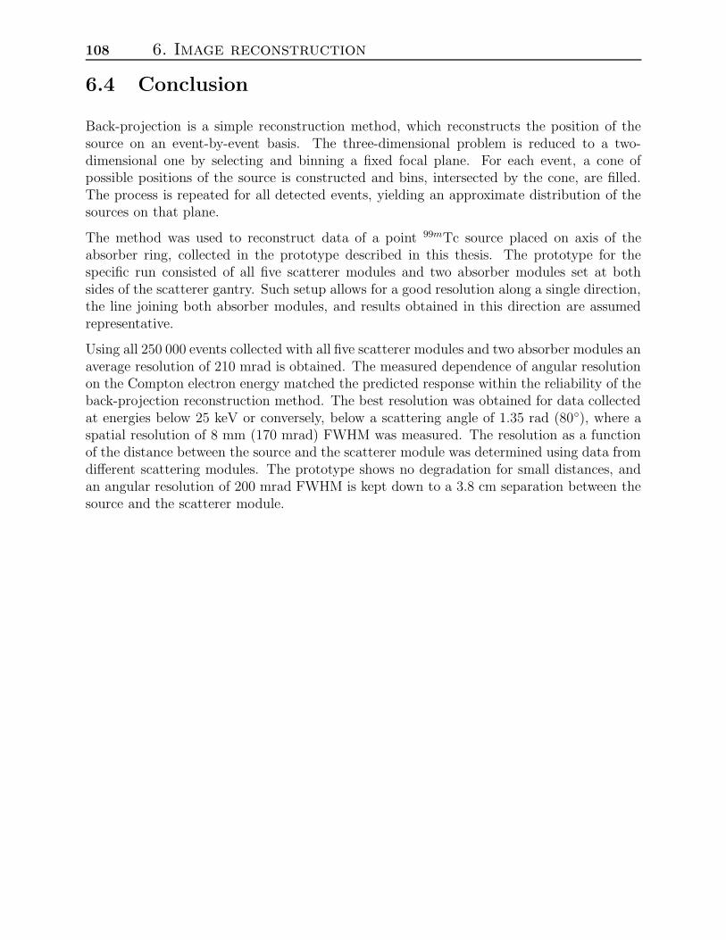
108 6. Image reconstruction
6.4 Conclusion
Back-projection is a simple reconstruction method, which reconstructs the position of thesource on an event-by-event basis. The three-dimensional problem is reduced to a two-dimensional one by selecting and binning a fixed focal plane. For each event, a cone ofpossible positions of the source is constructed and bins, intersected by the cone, are filled.The process is repeated for all detected events, yielding an approximate distribution of thesources on that plane.
The method was used to reconstruct data of a point 99mTc source placed on axis of theabsorber ring, collected in the prototype described in this thesis. The prototype for thespecific run consisted of all five scatterer modules and two absorber modules set at bothsides of the scatterer gantry. Such setup allows for a good resolution along a single direction,the line joining both absorber modules, and results obtained in this direction are assumedrepresentative.
Using all 250 000 events collected with all five scatterer modules and two absorber modules anaverage resolution of 210 mrad is obtained. The measured dependence of angular resolutionon the Compton electron energy matched the predicted response within the reliability of theback-projection reconstruction method. The best resolution was obtained for data collectedat energies below 25 keV or conversely, below a scattering angle of 1.35 rad (80), where aspatial resolution of 8 mm (170 mrad) FWHM was measured. The resolution as a functionof the distance between the source and the scatterer module was determined using data fromdifferent scattering modules. The prototype shows no degradation for small distances, andan angular resolution of 200 mrad FWHM is kept down to a 3.8 cm separation between thesource and the scatterer module.
Chapter 7
Prototype evaluation
The imaging based on the Compton camera principle is a novel technique of SPECT imaging,used to reconstruct spatial distribution of γ-rays sources. As it requires no mechanical colli-mator between the sources and the detector it effectively overcomes the efficiency-resolutiontrade-off imposed by mechanically collimated imaging devices, i.e. Anger cameras. The imag-ing performance of Compton camera improves with growing energy of the initial photons,which may fuel the development of radio-pharmaceuticals with larger gamma-ray energies,where the imaging is less influenced by photon scatter in the patient’s tissue.
The presented thesis focused on development of a suitable primary detector, the scatterer, fora Compton camera. Silicon pad sensors with optimized detector geometry and read-out weredeveloped and found to meet the harsh requirements for a Compton camera scatterer. Theabsorber of the prototype on the other hand consisted of modules designed for a differentsetup, but fitting nicely to our requirements. The prototype was assembled on a custommade mechanical frame and the data acquisition system consisted partially of custom madeelectronics and partially of off-shelf integrated circuits. All parts of the setup were tested andcalibrated prior to prototype operation, and the calibration data was used to improve andevaluate module performance. The assembled prototype was tested using point-like radio-active sources emitting photons of energies used for SPECT imaging. Image reconstructionwas performed using a simple back-projection algorithm and spatial resolution of down to170 mrad FWHM (for the optimal scattering angle range) was determined for a point source,which is in good agreement with expected performance.
This chapter evaluates the imaging performance of the presented Compton camera proto-type, together with individual sub-detector performance. There are two main evaluationparameters of a Compton camera setup: its spatial resolution and efficiency. Both will bediscussed in turn, along with possible upgrades of presented simple device to a more sophis-ticated Compton camera application. A comparison with elaborate Anger cameras is givenshowing how competitive Compton imaging is, even for a very crude prototype.
109
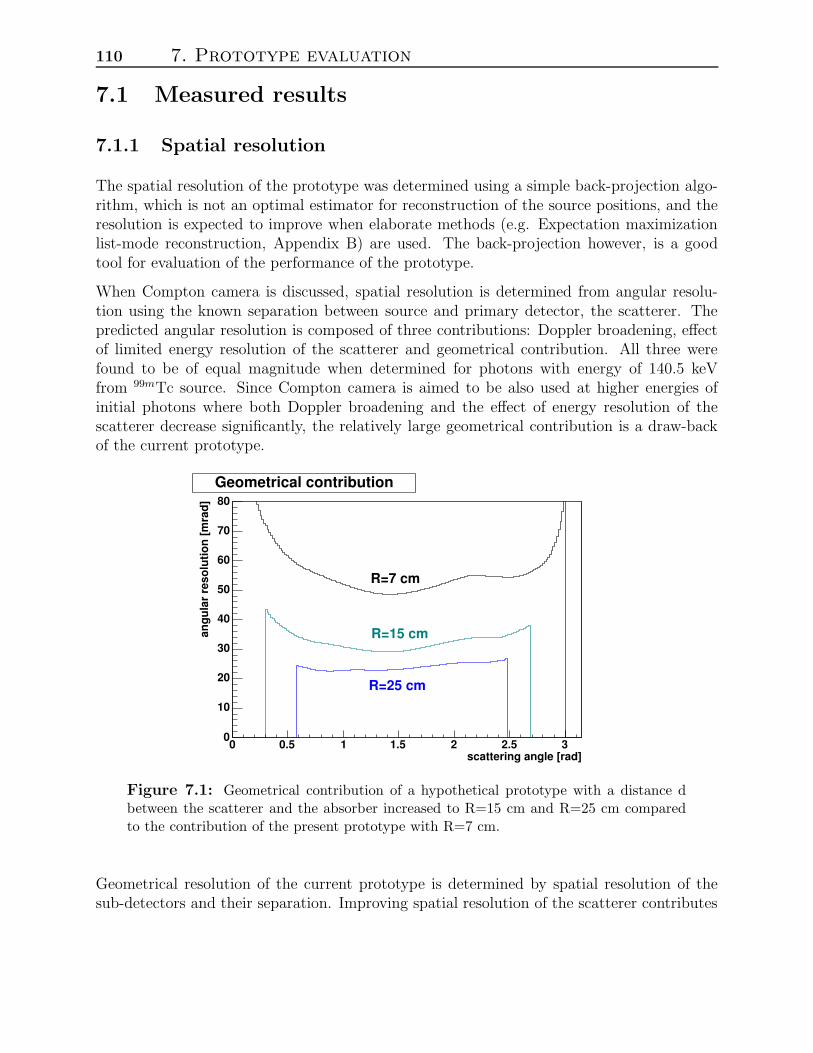
110 7. Prototype evaluation
7.1 Measured results
7.1.1 Spatial resolution
The spatial resolution of the prototype was determined using a simple back-projection algo-rithm, which is not an optimal estimator for reconstruction of the source positions, and theresolution is expected to improve when elaborate methods (e.g. Expectation maximizationlist-mode reconstruction, Appendix B) are used. The back-projection however, is a goodtool for evaluation of the performance of the prototype.
When Compton camera is discussed, spatial resolution is determined from angular resolu-tion using the known separation between source and primary detector, the scatterer. Thepredicted angular resolution is composed of three contributions: Doppler broadening, effectof limited energy resolution of the scatterer and geometrical contribution. All three werefound to be of equal magnitude when determined for photons with energy of 140.5 keVfrom 99mTc source. Since Compton camera is aimed to be also used at higher energies ofinitial photons where both Doppler broadening and the effect of energy resolution of thescatterer decrease significantly, the relatively large geometrical contribution is a draw-backof the current prototype.
scattering angle [rad]0 0.5 1 1.5 2 2.5 3
angu
lar
reso
lutio
n [m
rad]
0
10
20
30
40
50
60
70
80Geometrical contribution
R=25 cm
R=15 cm
R=7 cm
Figure 7.1: Geometrical contribution of a hypothetical prototype with a distance dbetween the scatterer and the absorber increased to R=15 cm and R=25 cm comparedto the contribution of the present prototype with R=7 cm.
Geometrical resolution of the current prototype is determined by spatial resolution of thesub-detectors and their separation. Improving spatial resolution of the scatterer contributes
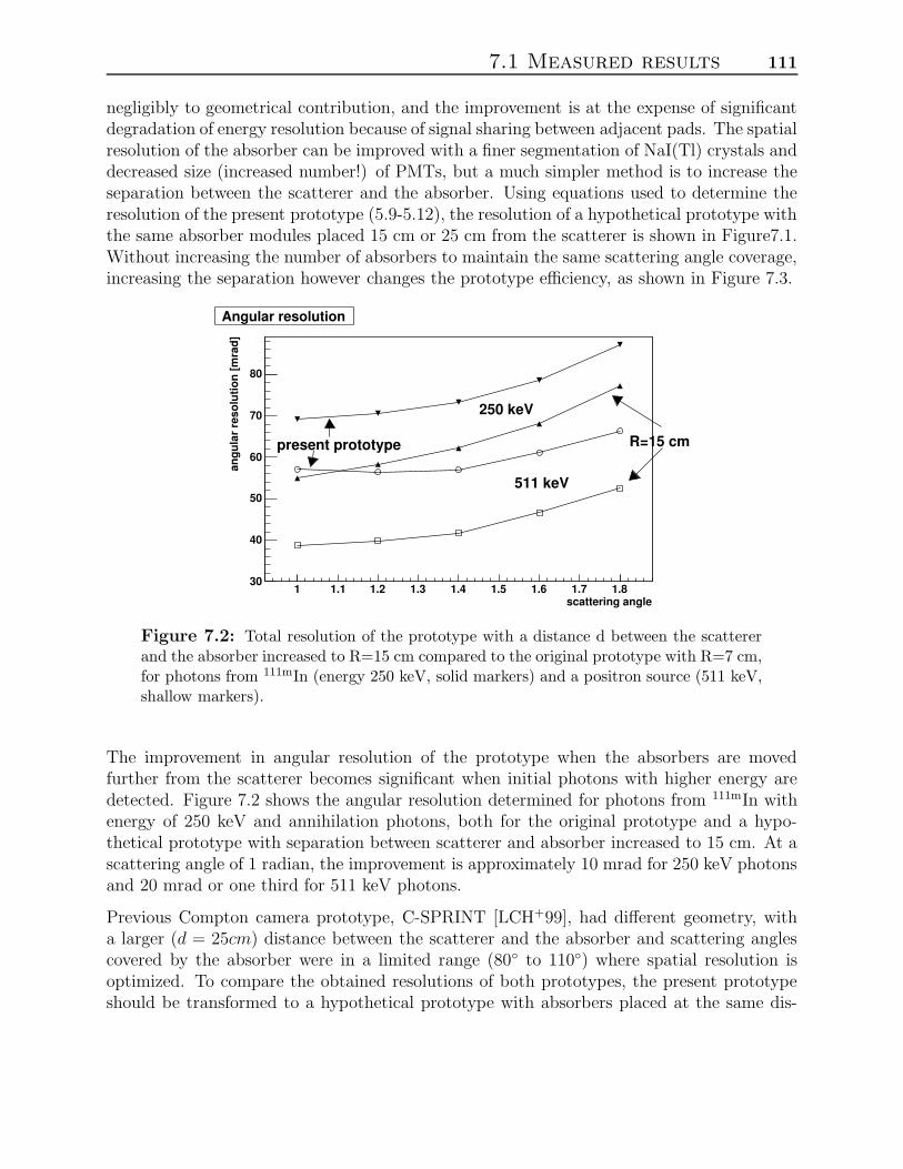
7.1 Measured results 111
negligibly to geometrical contribution, and the improvement is at the expense of significantdegradation of energy resolution because of signal sharing between adjacent pads. The spatialresolution of the absorber can be improved with a finer segmentation of NaI(Tl) crystals anddecreased size (increased number!) of PMTs, but a much simpler method is to increase theseparation between the scatterer and the absorber. Using equations used to determine theresolution of the present prototype (5.9-5.12), the resolution of a hypothetical prototype withthe same absorber modules placed 15 cm or 25 cm from the scatterer is shown in Figure7.1.Without increasing the number of absorbers to maintain the same scattering angle coverage,increasing the separation however changes the prototype efficiency, as shown in Figure 7.3.
scattering angle1 1.1 1.2 1.3 1.4 1.5 1.6 1.7 1.8
angu
lar
reso
lutio
n [m
rad]
30
40
50
60
70
80
Angular resolution
R=15 cm
250 keV
511 keV
present prototype
Figure 7.2: Total resolution of the prototype with a distance d between the scattererand the absorber increased to R=15 cm compared to the original prototype with R=7 cm,for photons from 111mIn (energy 250 keV, solid markers) and a positron source (511 keV,shallow markers).
The improvement in angular resolution of the prototype when the absorbers are movedfurther from the scatterer becomes significant when initial photons with higher energy aredetected. Figure 7.2 shows the angular resolution determined for photons from 111mIn withenergy of 250 keV and annihilation photons, both for the original prototype and a hypo-thetical prototype with separation between scatterer and absorber increased to 15 cm. At ascattering angle of 1 radian, the improvement is approximately 10 mrad for 250 keV photonsand 20 mrad or one third for 511 keV photons.
Previous Compton camera prototype, C-SPRINT [LCH+99], had different geometry, witha larger (d = 25cm) distance between the scatterer and the absorber and scattering anglescovered by the absorber were in a limited range (80 to 110) where spatial resolution isoptimized. To compare the obtained resolutions of both prototypes, the present prototypeshould be transformed to a hypothetical prototype with absorbers placed at the same dis-
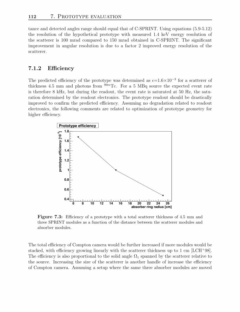
112 7. Prototype evaluation
tance and detected angles range should equal that of C-SPRINT. Using equations (5.9-5.12)the resolution of the hypothetical prototype with measured 1.4 keV energy resolution ofthe scatterer is 100 mrad compared to 150 mrad obtained in C-SPRINT. The significantimprovement in angular resolution is due to a factor 2 improved energy resolution of thescatterer.
7.1.2 Efficiency
The predicted efficiency of the prototype was determined as ε=1.6×10⁻³ for a scatterer ofthickness 4.5 mm and photons from 99mTc. For a 5 MBq source the expected event rateis therefore 8 kHz, but during the readout, the event rate is saturated at 50 Hz, the satu-ration determined by the readout electronics. The prototype readout should be drasticallyimproved to confirm the predicted efficiency. Assuming no degradation related to readoutelectronics, the following comments are related to optimization of prototype geometry forhigher efficiency.
absorber ring radius [cm]6 8 10 12 14 16 18 20 22 24 26
]-3
prot
otyp
e ef
ficie
ncy
[10
0.4
0.6
0.8
1
1.2
1.4
1.6
1.8Prototype efficiency
Figure 7.3: Efficiency of a prototype with a total scatterer thickness of 4.5 mm andthree SPRINT modules as a function of the distance between the scatterer modules andabsorber modules.
The total efficiency of Compton camera would be further increased if more modules would bestacked, with efficiency growing linearly with the scatterer thickness up to 1 cm [LCH+98].The efficiency is also proportional to the solid angle Ω1 spanned by the scatterer relative tothe source. Increasing the size of the scatterer is another handle of increase the efficiencyof Compton camera. Assuming a setup where the same three absorber modules are moved

7.1 Measured results 113
Table 7.1: Efficiency of the prototype for photons of commonly used radio-tracers99mTc (140.5 keV), 111mI (250 keV) and a positron source.
photon efficiency of the scatterer [4.5 mm] efficiency totalenergy [keV] + geometry [h] of the absorber [%] efficiency [h]
140.5 1.7 88 1.5250 1.4 60 0.83511 1.0 10 0.1
further from the source to increase the spatial resolution and optimal electronic readout, theefficiency is halved for a doubled (d=15 cm) distance between the scatterer and the absorber,or quartered if the absorbers are placed d=25 cm away from the scatterer The hypotheticalefficiency would hence be maintained by strategic placement of twice (four-times) the numberof absorber modules at the specified distance.
The hypothetical performance of the prototype with improved electronic when used withhigher energies of the initial photon is given in Table 7.1. The major efficiency loss at thoseenergies is due to the low stopping power of the absorber.
7.1.3 Comparison to Anger camera
Figure 7.4: A schematic drawing of an Anger camera [Ang58].
114 7. Prototype evaluation
Gamma cameras for clinical use are based on the Anger camera principle, described byHal Anger [Ang58] in the 1950-s. Figure 7.4 shows a schematic of the basic prototype: amechanical collimator of lead shields the sensitive part, a scintillator - photomultiplier tubeassembly, and only photons coming through the aperture are detected. The distribution ofinteractions on the sensitive plane is proportional to a two-dimensional projection of thespatial distribution of photon sources on the sensitive surface. A three-dimensional image isobtained by rotation of camera around the object.
Both efficiency and spatial resolution of the device depend on the aperture size. A largeaperture increases efficiency at the expense of spatial resolution. The opposite is true for asmall aperture, where higher spatial resolution is achieved1 at the expense of lower efficiency,causing the already mentioned resolution-efficiency trade-off, characteristic for mechanicallycollimated imaging. This trade-off causes operating devices to assume either a high-efficiency(HE) or high-resolution (HR) modality: in HE mode the efficiency is optimized while main-taining a reasonable image resolution, and in HR mode, resolution is optimized. Comparisonof performance parameters of both modalities in the state-of-the-art Anger cameras is givenin Table 7.2. For comparison, values for Anger camera optimized for imaging of small ani-mals is shown. This camera works in extreme proximity of the imaged objects, allowing itexhibit extreme spatial resolution and efficiency.
Table 7.2: Comparison of performance parameters of reported Anger cameras andCompton camera prototype at imaging of photons from 99mTc.
Camera type Spatial Efficiencyresolution [mm FWHM] [h]
Siemens low-energy HR 5 [GFD+96] ≈ 0.05Orbiter2 HE 11 [GFD+96] 0.1-0.2fastSPECT [LKS+02] 1.5 0.4Compton camera prototype 10 1.5 (0.04)
Comparing our simple prototype to elaborate devices presented in Table 7.2 seems like afutile task. The Anger camera principle is present for 50 years and many solutions werefound to circumvent the draw-backs of the basic principle. Compton camera, however, isa new imaging method with practically no experience, and current prototype is aimed atconfirming its principles rather than excelling in performance. The fact that parametersare comparable (Table 7.2) for a simple prototype with geometry and readout far fromoptimized and a very simple image reconstruction technique, makes Compton camera a verypopular tool for the future. When radio-tracers with photon energies higher than 140.5 keV(used for comparison in Table 7.2) are used, performance of Compton camera improves,and performance of Anger camera degrades. Therefore Compton camera offers a whole new
1The spatial resolution of an Anger camera is saturated at the inherent resolution of the sensitive part.
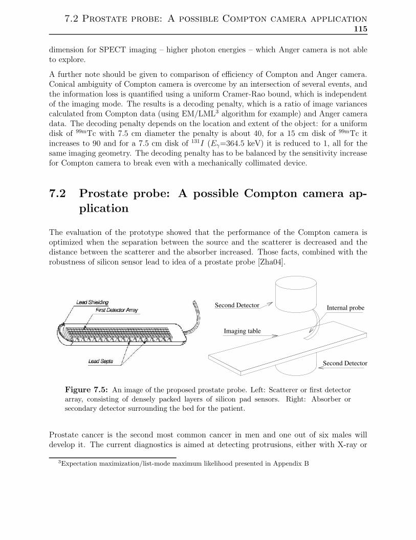
7.2 Prostate probe: A possible Compton camera application115
dimension for SPECT imaging – higher photon energies – which Anger camera is not ableto explore.
A further note should be given to comparison of efficiency of Compton and Anger camera.Conical ambiguity of Compton camera is overcome by an intersection of several events, andthe information loss is quantified using a uniform Cramer-Rao bound, which is independentof the imaging mode. The results is a decoding penalty, which is a ratio of image variancescalculated from Compton data (using EM/LML3 algorithm for example) and Anger cameradata. The decoding penalty depends on the location and extent of the object: for a uniformdisk of 99mTc with 7.5 cm diameter the penalty is about 40, for a 15 cm disk of 99mTc itincreases to 90 and for a 7.5 cm disk of 131I (Eγ=364.5 keV) it is reduced to 1, all for thesame imaging geometry. The decoding penalty has to be balanced by the sensitivity increasefor Compton camera to break even with a mechanically collimated device.
7.2 Prostate probe: A possible Compton camera ap-
plication
The evaluation of the prototype showed that the performance of the Compton camera isoptimized when the separation between the source and the scatterer is decreased and thedistance between the scatterer and the absorber increased. Those facts, combined with therobustness of silicon sensor lead to idea of a prostate probe [Zha04].
Second Detector
Second Detector
Internal probe
Imaging table
Figure 7.5: An image of the proposed prostate probe. Left: Scatterer or first detectorarray, consisting of densely packed layers of silicon pad sensors. Right: Absorber orsecondary detector surrounding the bed for the patient.
Prostate cancer is the second most common cancer in men and one out of six males willdevelop it. The current diagnostics is aimed at detecting protrusions, either with X-ray or
3Expectation maximization/list-mode maximum likelihood presented in Appendix B
116 7. Prototype evaluation
ultrasound. Currently, SPECT imaging is only used to trace the spreading of the disease toother organs [KWM+98, HBO+98], which is already a critical phase in cancer development.Present cameras placed 10 cm of further from the prostate do not exhibit required spatialresolution to determine the extent and location of the primary tumor. The prostate probewould be hence a pioneer in the field, exploiting both a near-field view of the prostate and aresulting high spatial resolution. A proposed probe could be composed as shown in Figure7.5: a densely packed array of silicon pad sensors with thickness of 10 mm to be insertedintra-rectally, close to the prostate, and an absorber ring with a radius of 25 cm surroundsthe body of the patient and detects the scattered photons. The radio-active agent usedwould be a 111mIn labeled antibody specific to prostate cancer, which is already used forpresent prostate-cancer related SPECT imaging.
The device is currently being modeled using Monte-Carlo studies. An elaborate computerphantom simulating the human body is used along with determined uptakes of radiationin other organs of the patient. The simulation shows the device efficiency equal to 1.8 h
and resolution of 2.58 mm FWHM. The prostate probe with such a performance wouldbe able to detect lesions with a 5 mm diameter and radio-tracer related activity 5-timeslarger than the activity of the background, allowing for early detection of the disease anda precise monitoring of its treatment. For a comparison, the best resolution obtained by acollimated scintillator ring would be 11 mm FWHM in high resolution mode and 15 mm inhigh efficiency mode, where estimated efficiency equals to 0.1 h.
Chapter 8
Summary
SPECT is a diagnostic method where spatial resolution of disease specific substances, labeledwith γ-ray sources is imaged. Traditional SPECT detectors, Anger cameras are limited intheir performance, since they exhibit resolution-efficiency trade-off inherent to mechanicallycollimated cameras. Compton camera is a novel imaging technique, which uses kinematicsof Compton scattering instead of mechanical collimator removing the coupling between effi-ciency and resolution. The thesis presents the development of a Compton camera prototypebuilt in order to test the viability of the proposed approach.
Compton camera consists of two sub-detectors: the scatterer where Compton scattering ofinitial photons is observed, and the absorber, where scattered photons are detected. InCompton scattering a Compton electron is produced, and kinematics relates the kineticenergy of the electron to the photon scattering angle. The scatterer measures the energy ofthe Compton electron, and impact points in scatterer and absorber determine the scatteredphoton direction. All possible directions of the initial photon form a cone, with the axisalong the scattered photon direction, the opening angle equal to the scattering angle andthe apex fixed on the interaction point in the scatterer. Intersection of cones for multipleevents reproduces the position of the source.
The spatial resolution of the device is driven by three contributions: inherent resolution fromDoppler broadening, limited energy resolution of the scatterer and geometrical contributionrelated to spatial resolution of sub-detectors. In an optimized imager the inherent resolutionis dominant and contributions of energy resolution of the scatterer and setup layout combinedwith spatial resolution of sub-detectors should be smaller.
The scatterer module of the developed prototype consists of custom developed silicon padsensors, coupled to VATAGP3, an off-the-shelf front-end ASIC. Silicon exhibits one of thelowest Doppler broadenings in detection materials (80 mrad at the scattering angle of π/2)and silicon pad sensors provide suitable energy resolution at room temperature and (morethan) adequate spatial resolution. A pad dimension of 1.4 mm was chosen to confine thecharge produced by a Compton electron to a single pad, minimizing the dominating contri-
117
118 8. Summary
bution of front-end electronics noise on energy resolution. Sensors with thicknesses of up to1 mm were used. Data were collected using a custom developed data acquisition system,partially based on VME technology. The excellent measured energy resolution of 1.2 keV on0.5 mm and 1.5 keV on 1 mm thick sensors gave a contribution to resolution approximatelyequal to Doppler broadening for 99mTc photons. The trigger signal of the scatterer, requiredfor correlation of interactions in the scatterer and the absorber, was measured to have atiming resolution of 150 ns FWHM.
The absorber of the setup was taken from the existing SPRINT II prototype, fitting nicelyto requirements of the Compton camera. The calibration of the absorber gave a spatialresolution of 4 mm FWHM and timing resolution of 22 ns FWHM.
The prototype was assembled on a custom designed frame. Five scatterer modules with atotal thickness of 4.5 mm were surrounded by three absorber modules forming an incompletering with an average separation of 7 cm between scatterer and absorber modules. A 99mTcsource was placed on axis of the ring, approximately 4 cm away from the first scatterer mod-ule. For such placement of the source, the predicted efficiency of the setup was 1.6×10⁻³
and the geometrical contribution to spatial resolution was approximately equal to the con-tribution from Doppler broadening. The timing resolution of the prototype was dominatedby the resolution of the scatterer and a timing window of 200 ns was used. Data from a5 MBq source were collected with a maximal event readout frequency of 50 Hz, saturateddue to the readout electronics.
A simple back-projection algorithm was used to reconstruct the position of the point source.The resolution of the reconstructed image matched the predicted resolution. For a limitednumber of events within the optimal scattering angle range, a spatial resolution of 8 mmFWHM was obtained, or angular resolution of 170 mrad FWHM, comparable to the per-formance of the state-of-the art Anger cameras. The estimated efficiency of the prototypewas an order of magnitude larger than efficiency of a typical Anger camera, which wouldcompensate for the conical ambiguity of Compton imaging reconstruction.
The performance of the simple prototype with a crude reconstruction algorithm was compa-rable to the performance of the state-of-the art Anger cameras, which shows a great potentialfor more elaborate Compton camera imagers. A proposed application, the prostate probewould consist of a densely packed scatterer, inserted intra-rectally with a near-field view ofthe prostate, combined with an absorber ring surrounding the patient. According to the sim-ulations, the probe would exhibits spatial resolution and efficiency superiror to the presentdetectors for higher energy (111mIn, 245.5 keV) radio-tracers specific to prostate cancer. Thusthe prostate probe should be capable of determining the location and extent of the primarycancer, a task present SPECT is not capable of, allowing for early treatment and precisemonitoring of the disease.
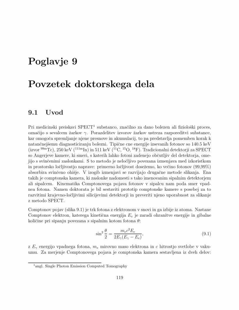
Poglavje 9
Povzetek doktorskega dela
9.1 Uvod
Pri medicinski preiskavi SPECT1 substanco, znacilno za dano bolezen ali fizioloski proces,oznacijo s sevalcem zarkov γ. Porazdelitev izvorov zarkov ustreza razporeditvi substance,kar omogoca spremljanje njene presnove in akumulacij, to pa predstavlja pomemben korak knatancnejsemu diagnosticiranju bolezni. Tipicne cne energije izsevanih fotonov so 140.5 keV(izvor 99mTc), 250 keV (111mIn) in 511 keV (11C, 15O, 18F). Tradicionalni detektorji za SPECTso Angerjeve kamere, ki smeri, s katerih lahko fotoni zadenejo obcutljiv del detektorja, ome-jijo s svincenimi zaslonkami. S to metodo je nelocljivo povezana izmenjava med izkoristkomin prostorsko locljivostjo naprave: primerno locljivost dosezemo, ko vecino fotonov (99,99%)absorbira svinceno ohisje. V izogib izmenjavi se razvijajo drugacne metode slikanja. Enatakih je comptonska kamera, ki zaslonke nadomesti s tako imenovanim sipalnim detektorjemali sipalcem. Kinematika Comptonovega pojava fotonov v sipalcu nam poda smer vpad-nea fotona. Namen doktorata je bil sestaviti prototip comptonske kamere s posebej za torazvitimi krajevno-locljivimi silicijevimi detektorji in preveriti njeno uporabnost za slikanjez metodo SPECT.
Comptonov pojav (slika 9.1) je trk fotona z elektronom v snovi in ga izbije iz atoma. NastaneComptonov elektron, katerega kineticna energija Ee je zaradi ohranitve energije in gibalnekolicine pri sipanju povezana s sipalnim kotom fotona θ:
sin2 θ
2=
mec2Ee
2Eγ(Eγ − Ee), (9.1)
z Eγ energijo vpadnega fotona, me mirovno maso elektrona in c hitrostjo svetlobe v vaku-umu. Za merjenje Comptonovega pojava je comptonska kamera sestavljena iz dveh delov:
1angl. Single Photon Emission Computed Tomography
119
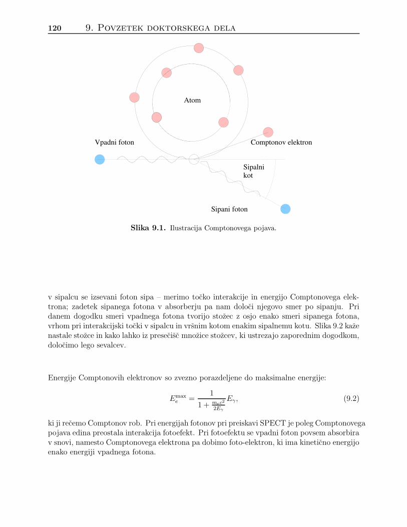
120 9. Povzetek doktorskega dela
Atom
Comptonov elektron
kotSipalni
Sipani foton
Vpadni foton
Slika 9.1. Ilustracija Comptonovega pojava.
v sipalcu se izsevani foton sipa – merimo tocko interakcije in energijo Comptonovega elek-trona; zadetek sipanega fotona v absorberju pa nam doloci njegovo smer po sipanju. Pridanem dogodku smeri vpadnega fotona tvorijo stozec z osjo enako smeri sipanega fotona,vrhom pri interakcijski tocki v sipalcu in vrsnim kotom enakim sipalnemu kotu. Slika 9.2 kazenastale stozce in kako lahko iz presecisc mnozice stozcev, ki ustrezajo zaporednim dogodkom,dolocimo lego sevalcev.
Energije Comptonovih elektronov so zvezno porazdeljene do maksimalne energije:
Emaxe =
1
1 + mec2
2Eγ
Eγ , (9.2)
ki ji recemo Comptonov rob. Pri energijah fotonov pri preiskavi SPECT je poleg Comptonovegapojava edina preostala interakcija fotoefekt. Pri fotoefektu se vpadni foton povsem absorbirav snovi, namesto Comptonovega elektrona pa dobimo foto-elektron, ki ima kineticno energijoenako energiji vpadnega fotona.
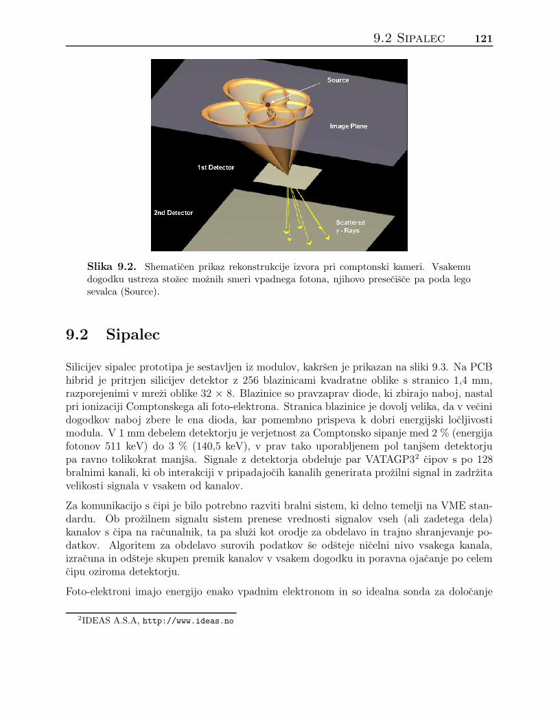
9.2 Sipalec 121
Slika 9.2. Shematicen prikaz rekonstrukcije izvora pri comptonski kameri. Vsakemudogodku ustreza stozec moznih smeri vpadnega fotona, njihovo presecisce pa poda legosevalca (Source).
9.2 Sipalec
Silicijev sipalec prototipa je sestavljen iz modulov, kakrsen je prikazan na sliki 9.3. Na PCBhibrid je pritrjen silicijev detektor z 256 blazinicami kvadratne oblike s stranico 1,4 mm,razporejenimi v mrezi oblike 32 × 8. Blazinice so pravzaprav diode, ki zbirajo naboj, nastalpri ionizaciji Comptonskega ali foto-elektrona. Stranica blazinice je dovolj velika, da v vecinidogodkov naboj zbere le ena dioda, kar pomembno prispeva k dobri energijski locljivostimodula. V 1 mm debelem detektorju je verjetnost za Comptonsko sipanje med 2 % (energijafotonov 511 keV) do 3 % (140,5 keV), v prav tako uporabljenem pol tanjsem detektorjupa ravno tolikokrat manjsa. Signale z detektorja obdeluje par VATAGP32 cipov s po 128bralnimi kanali, ki ob interakciji v pripadajocih kanalih generirata prozilni signal in zadrzitavelikosti signala v vsakem od kanalov.
Za komunikacijo s cipi je bilo potrebno razviti bralni sistem, ki delno temelji na VME stan-dardu. Ob prozilnem signalu sistem prenese vrednosti signalov vseh (ali zadetega dela)kanalov s cipa na racunalnik, ta pa sluzi kot orodje za obdelavo in trajno shranjevanje po-datkov. Algoritem za obdelavo surovih podatkov se odsteje nicelni nivo vsakega kanala,izracuna in odsteje skupen premik kanalov v vsakem dogodku in poravna ojacanje po celemcipu oziroma detektorju.
Foto-elektroni imajo energijo enako vpadnim elektronom in so idealna sonda za dolocanje
2IDEAS A.S.A, http://www.ideas.no
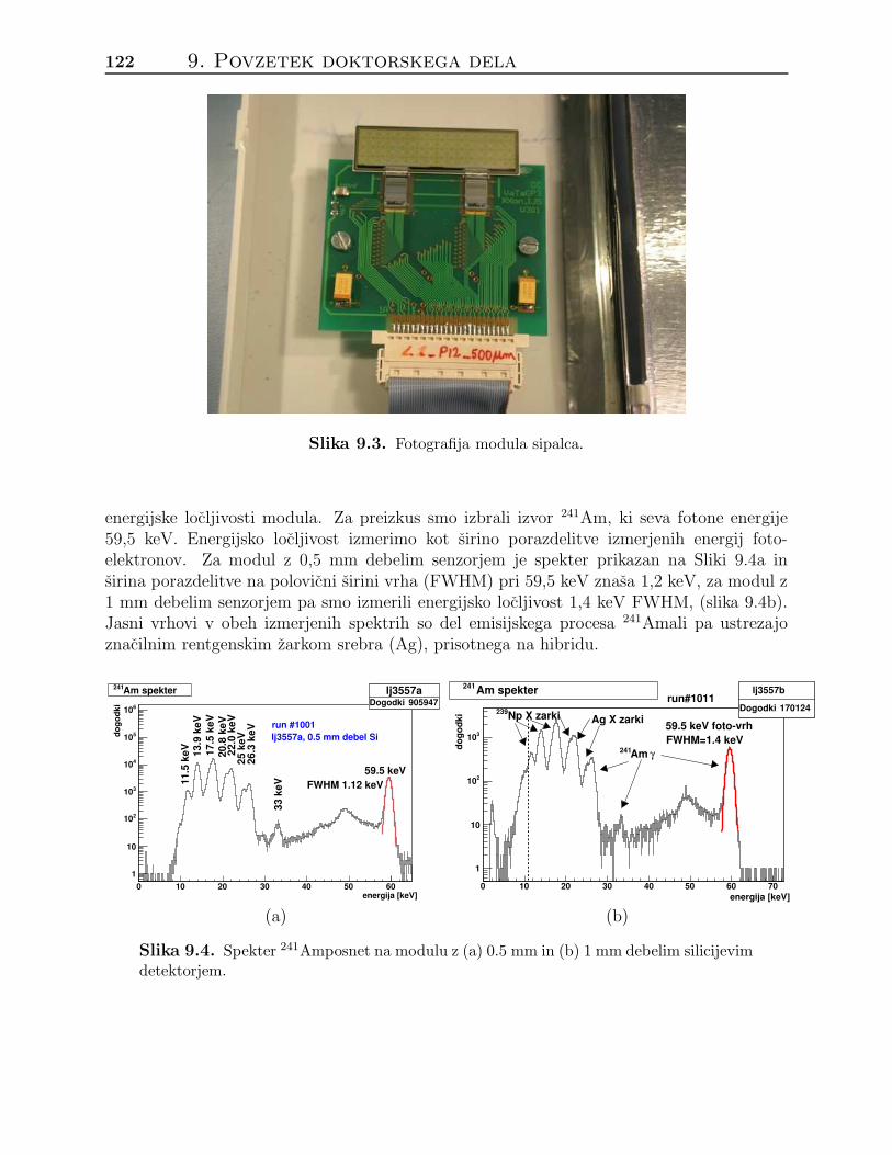
122 9. Povzetek doktorskega dela
Slika 9.3. Fotografija modula sipalca.
energijske locljivosti modula. Za preizkus smo izbrali izvor 241Am, ki seva fotone energije59,5 keV. Energijsko locljivost izmerimo kot sirino porazdelitve izmerjenih energij foto-elektronov. Za modul z 0,5 mm debelim senzorjem je spekter prikazan na Sliki 9.4a insirina porazdelitve na polovicni sirini vrha (FWHM) pri 59,5 keV znasa 1,2 keV, za modul z1 mm debelim senzorjem pa smo izmerili energijsko locljivost 1,4 keV FWHM, (slika 9.4b).Jasni vrhovi v obeh izmerjenih spektrih so del emisijskega procesa 241Amali pa ustrezajoznacilnim rentgenskim zarkom srebra (Ag), prisotnega na hibridu.
lj3557aDogodki 905947
energija [keV]0 10 20 30 40 50 60
dogo
dki
1
10
210
310
410
510
610
lj3557aDogodki 905947
Am spekter241
11.5
keV 13
.9 k
eV17
.5 k
eV20
.8 k
eV22
.0 k
eV25
keV
26.3
keV
33 k
eV
59.5 keVFWHM 1.12 keV
lj3557a, 0.5 mm debel Sirun #1001
lj3557b
Dogodki 170124
0 10 20 30 40 50 60 70
1
10
210
310
lj3557b
Dogodki 170124
dogo
dki
energija [keV]
241Am spekter
59.5 keV foto-vrhFWHM=1.4 keV
Np X zarki239Ag X zarki
γAm 241
run#1011
(a) (b)
Slika 9.4. Spekter 241Amposnet na modulu z (a) 0.5 mm in (b) 1 mm debelim silicijevimdetektorjem.
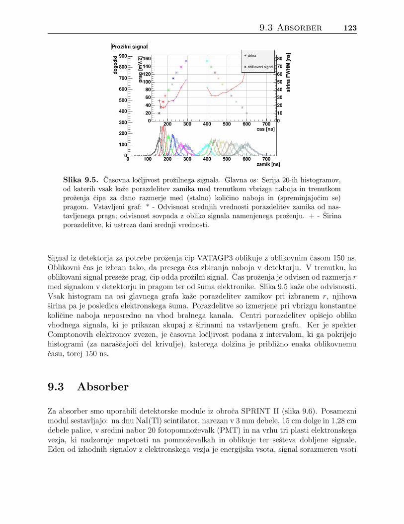
9.3 Absorber 123
zamik [ns]0 100 200 300 400 500 600 700
dogo
dki
0
100
200
300
400
500
600
700
800
900
Prozilni signal
siri
na F
WH
M [n
s]
010
20
30
4050
6070
80
prag
[mV
/2]
020
40
60
80100
120140
160
cas [ns]200 300 400 500 600 700
sirina
oblikovani signal
Slika 9.5. Casovna locljivost prozilnega signala. Glavna os: Serija 20-ih histogramov,od katerih vsak kaze porazdelitev zamika med trenutkom vbrizga naboja in trenutkomprozenja cipa za dano razmerje med (stalno) kolicino naboja in (spreminjajocim se)pragom. Vstavljeni graf: * - Odvisnost srednjih vrednosti porazdelitev zamika od nas-tavljenega praga; odvisnost sovpada z obliko signala namenjenega prozenju. + - Sirinaporazdelitve, ki ustreza dani srednji vrednosti.
Signal iz detektorja za potrebe prozenja cip VATAGP3 oblikuje z oblikovnim casom 150 ns.Oblikovni cas je izbran tako, da presega cas zbiranja naboja v detektorju. V trenutku, kooblikovani signal preseze prag, cip odda prozilni signal. Cas prozenja je odvisen od razmerja rmed signalom v detektorju in pragom ter od suma elektronike. Slika 9.5 kaze obe odvisnosti.Vsak histogram na osi glavnega grafa kaze porazdelitev zamikov pri izbranem r, njihovasirina pa je posledica elektronskega suma. Porazdelitve so izmerjene pri vbrizgu konstantnekolicine naboja neposredno na vhod bralnega kanala. Centri porazdelitev opisejo oblikovhodnega signala, ki je prikazan skupaj z sirinami na vstavljenem grafu. Ker je spekterComptonovih elektronov zvezen, je casovna locljivost podana z intervalom, ki ga pokrijejohistogrami (za narascajoci del krivulje), katerega dolzina je priblizno enaka oblikovnemucasu, torej 150 ns.
9.3 Absorber
Za absorber smo uporabili detektorske module iz obroca SPRINT II (slika 9.6). Posameznimodul sestavljajo: na dnu NaI(Tl) scintilator, narezan v 3 mm debele, 15 cm dolge in 1,28 cmdebele palice, v sredini nabor 20 fotopomnozevalk (PMT) in na vrhu tri plasti elektronskegavezja, ki nadzoruje napetosti na pomnozevalkah in oblikuje ter sesteva dobljene signale.Eden od izhodnih signalov z elektronskega vezja je energijska vsota, signal sorazmeren vsoti
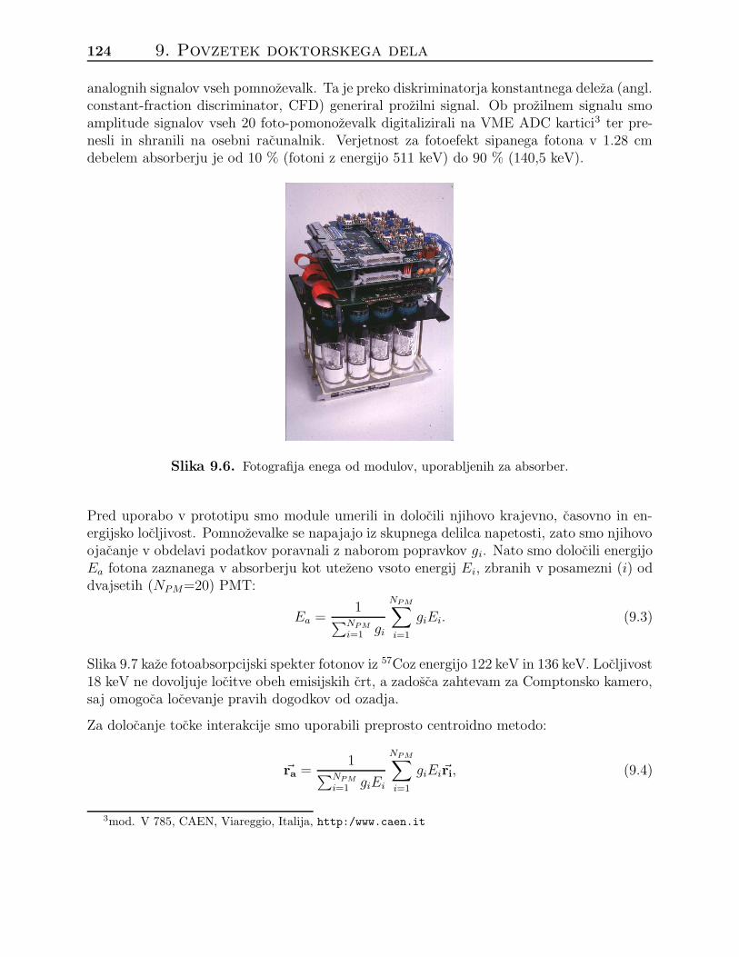
124 9. Povzetek doktorskega dela
analognih signalov vseh pomnozevalk. Ta je preko diskriminatorja konstantnega deleza (angl.constant-fraction discriminator, CFD) generiral prozilni signal. Ob prozilnem signalu smoamplitude signalov vseh 20 foto-pomonozevalk digitalizirali na VME ADC kartici3 ter pre-nesli in shranili na osebni racunalnik. Verjetnost za fotoefekt sipanega fotona v 1.28 cmdebelem absorberju je od 10 % (fotoni z energijo 511 keV) do 90 % (140,5 keV).
Slika 9.6. Fotografija enega od modulov, uporabljenih za absorber.
Pred uporabo v prototipu smo module umerili in dolocili njihovo krajevno, casovno in en-ergijsko locljivost. Pomnozevalke se napajajo iz skupnega delilca napetosti, zato smo njihovoojacanje v obdelavi podatkov poravnali z naborom popravkov gi. Nato smo dolocili energijoEa fotona zaznanega v absorberju kot utezeno vsoto energij Ei, zbranih v posamezni (i) oddvajsetih (NPM=20) PMT:
Ea =1
∑NPM
i=1 gi
NPM∑
i=1
giEi. (9.3)
Slika 9.7 kaze fotoabsorpcijski spekter fotonov iz 57Coz energijo 122 keV in 136 keV. Locljivost18 keV ne dovoljuje locitve obeh emisijskih crt, a zadosca zahtevam za Comptonsko kamero,saj omogoca locevanje pravih dogodkov od ozadja.
Za dolocanje tocke interakcije smo uporabili preprosto centroidno metodo:
~ra =1
∑NPM
i=1 giEi
NPM∑
i=1
giEi~ri, (9.4)
3mod. V 785, CAEN, Viareggio, Italija, http:/www.caen.it
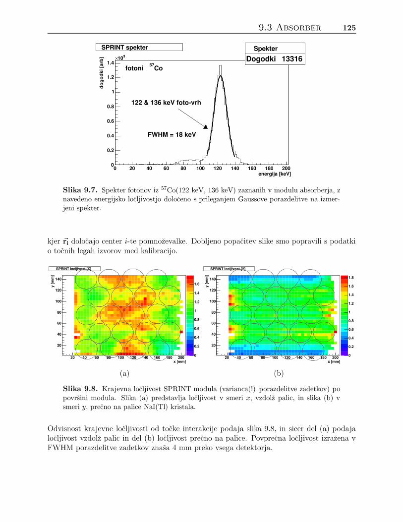
9.3 Absorber 125
Spekter
Dogodki 13316
energija [keV]0 20 40 60 80 100 120 140 160 180 200
dogo
dki [
arb]
0
0.2
0.4
0.6
0.8
1
1.2
1.4310×
Spekter
Dogodki 13316SPRINT spekter
Co57fotoni
122 & 136 keV foto-vrh
FWHM = 18 keV
Slika 9.7. Spekter fotonov iz 57Co(122 keV, 136 keV) zaznanih v modulu absorberja, znavedeno energijsko locljivostjo doloceno s prileganjem Gaussove porazdelitve na izmer-jeni spekter.
kjer ~ri dolocajo center i-te pomnozevalke. Dobljeno popacitev slike smo popravili s podatkio tocnih legah izvorov med kalibracijo.
x [mm]20 40 60 80 100 120 140 160 180 200
y [m
m]
20
40
60
80
100
120
140
0
0.2
0.4
0.6
0.8
1
1.2
1.4
1.6
SPRINT locljivost [X]
(a)
x [mm]20 40 60 80 100 120 140 160 180 200
y [m
m]
20
40
60
80
100
120
140
0
0.2
0.4
0.6
0.8
1
1.2
1.4
1.6
1.8
SPRINT locljivost [Y]
(b)
Slika 9.8. Krajevna locljivost SPRINT modula (varianca(!) porazdelitve zadetkov) popovrsini modula. Slika (a) predstavlja locljivost v smeri x, vzdolz palic, in slika (b) vsmeri y, precno na palice NaI(Tl) kristala.
Odvisnost krajevne locljivosti od tocke interakcije podaja slika 9.8, in sicer del (a) podajalocljivost vzdolz palic in del (b) locljivost precno na palice. Povprecna locljivost izrazena vFWHM porazdelitve zadetkov znasa 4 mm preko vsega detektorja.
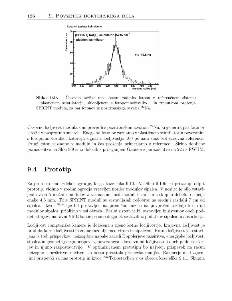
126 9. Povzetek doktorskega dela
casovna razlika [ns]540 560 580 600 620 640 660 680 700 720
Zade
tki n
a 1
ns
0
20
40
60
80
100
Casovni spekter koincidenc
= 10.6 nsσ
2[SPRINT] NaI(Tl) scintilator 15x15 cmplasticni scintilator
Slika 9.9. Casovna razlike med casom zadetka fotona v referencnem sistemu– plasticnem scintilatorju, sklopljenem s fotopomnozevalko – in trenutkom prozenjaSPRINT modula, za par fotonov iz pozitronskega sevalca 22Na.
Casovno locljivost modula smo preverili s pozitronskim izvorom 22Na, ki generira par fotonovletecih v nasprotnih smereh. Enega od fotonov zaznamo v plasticnem scintilatorju povezanims fotopomnozevalko, katerega signal z locljivostjo 100 ps nam sluzi kot casovna referenca.Drugi foton zaznamo v modulu in cas prozenja primerjamo z referenco. Sirino dobljeneporazdelitve na Sliki 9.9 smo dolocili s prileganjem Gaussove porazdelitve na 22 ns FWHM.
9.4 Prototip
Za prototip smo izdelali ogrodje, ki ga kaze slika 9.10. Na Sliki 9.10b, ki prikazuje odprtprototip, vidimo v sredini ogrodja vstavljen nosilec modulov sipalca. V nosilec je bilo vstavl-jenih vseh 5 moznih modulov z razmakom med moduli 6 mm in s skupno debelino silicijaenako 4,5 mm. Trije SPRINT moduli so sestavljajali polobroc na srednji razdalji 7 cm odsipalca. Izvor 99mTcje bil postavljen na premicno mizico na povprecni razdalji 5 cm odmodulov sipalca, priblizno v osi obroca. Bralni sistem je bil sestavljen iz sistemov obeh pod-detektorjev, na ravni VME kartic pa smo dogodek sestavili iz podatkov sipalca in absorberja.
Locljivost comptonske kamere je dolocena z njeno kotno locljivostjo; krajevna locljivost jeprodukt kotne locljivosti in znane razdalje med virom in sipalcem. Kotna locljivost je sestavl-jena iz treh prispevkov: neizogibne napake zaradi Dopplerjeve razsiritve, energijske locljivostisipalca in geometrijskega prispevka, povezanega s krajevnimi locljivostmi obeh poddetektor-jev in njuno razpostavitvijo. V optimiziranem prototipu bo najvecji prispevek na racunneizogibne razsiritve, medtem ko bosta preostala prispevka manjsa. Razmerje med zgorn-jimi prispevki za nas prototip in izvor 99mTcpostavljen v os obroca kaze slika 9.11. Skupna
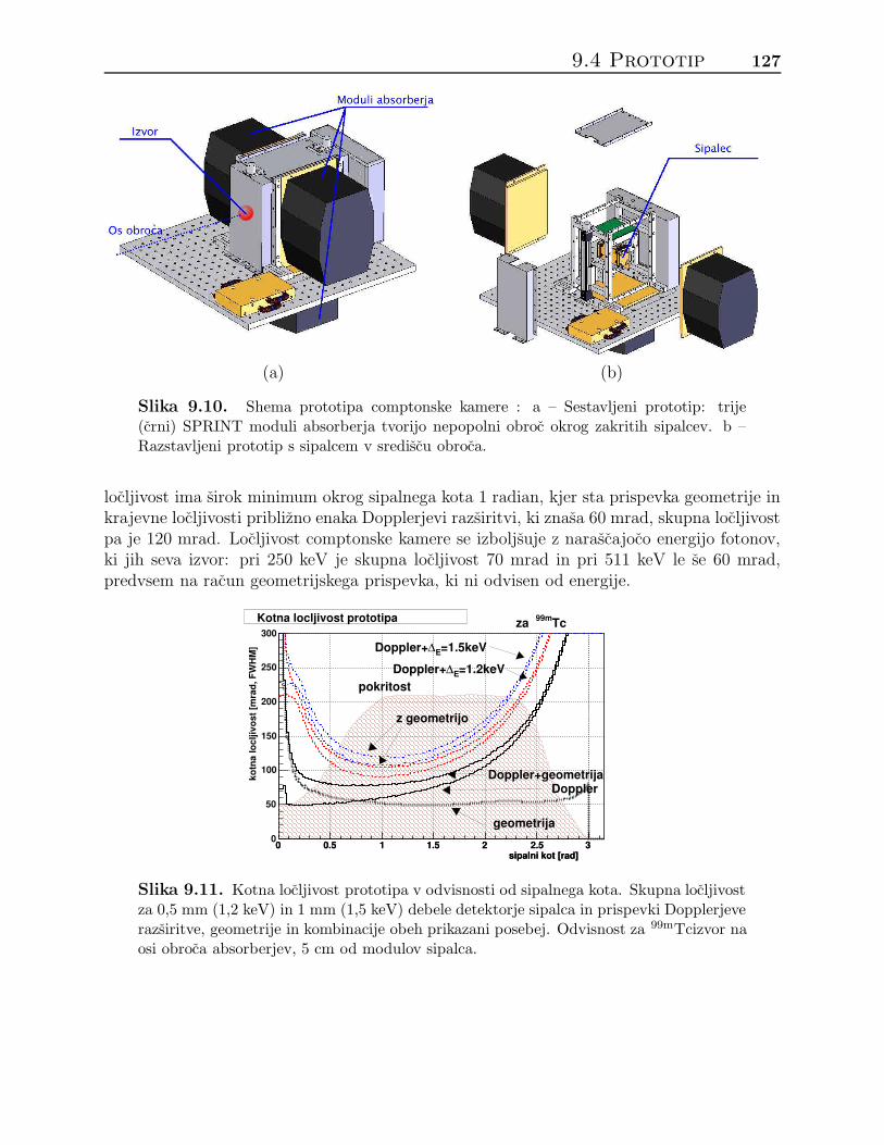
9.4 Prototip 127
(a) (b)
Slika 9.10. Shema prototipa comptonske kamere : a – Sestavljeni prototip: trije(crni) SPRINT moduli absorberja tvorijo nepopolni obroc okrog zakritih sipalcev. b –Razstavljeni prototip s sipalcem v srediscu obroca.
locljivost ima sirok minimum okrog sipalnega kota 1 radian, kjer sta prispevka geometrije inkrajevne locljivosti priblizno enaka Dopplerjevi razsiritvi, ki znasa 60 mrad, skupna locljivostpa je 120 mrad. Locljivost comptonske kamere se izboljsuje z narascajoco energijo fotonov,ki jih seva izvor: pri 250 keV je skupna locljivost 70 mrad in pri 511 keV le se 60 mrad,predvsem na racun geometrijskega prispevka, ki ni odvisen od energije.
sipalni kot [rad]0 0.5 1 1.5 2 2.5 3
sipalni kot [rad]0 0.5 1 1.5 2 2.5 3
kotn
a lo
cljiv
ost [
mra
d, F
WH
M]
0
50
100
150
200
250
300
Doppler+geometrijaDoppler
geometrija
z geometrijo
=1.5keVE∆Doppler+
=1.2keVE∆Doppler+pokritost
Tc99mza Kotna locljivost prototipa
Slika 9.11. Kotna locljivost prototipa v odvisnosti od sipalnega kota. Skupna locljivostza 0,5 mm (1,2 keV) in 1 mm (1,5 keV) debele detektorje sipalca in prispevki Dopplerjeverazsiritve, geometrije in kombinacije obeh prikazani posebej. Odvisnost za 99mTcizvor naosi obroca absorberjev, 5 cm od modulov sipalca.
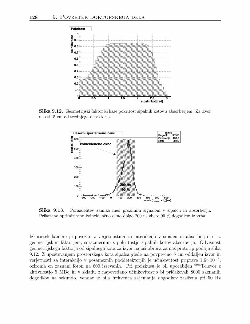
128 9. Povzetek doktorskega dela
sipalni kot [rad]0 0.5 1 1.5 2 2.5 3
sipalni kot [rad]0 0.5 1 1.5 2 2.5 3
ucin
kovi
tost
0
0.1
0.2
0.3
0.4
0.5
0.6
0.7
0.8
0.9
1
Pokritost
Slika 9.12. Geometrijski faktor ki kaze pokritost sipalnih kotov z absorberjem. Za izvorna osi, 5 cm od srednjega detektorja.
zamikEntries 36951Mean 158.8RMS 80.06
)[ns]Si - tSPRINTzamik (t-300 -200 -100 0 100 200 300 400 500 600
dogo
dki [
arb]
0
100
200
300
400
500
600
zamikEntries 36951Mean 158.8RMS 80.06
Casovni spekter koincidenc zamikDogodki 36951Povprecje 158.8RMS 80.06
90 %200 ns
koincidencno okno
Slika 9.13. Porazdelitev zamika med prozilnim signalom v sipalcu in absorberju.Prikazano optimizirano koincidencno okno dolgo 200 ns zbere 90 % dogodkov iz vrha.
Izkoristek kamere je povezan z verjetnostma za interakcijo v sipalcu in absorberju ter zgeometrijskim faktorjem, sorazmernim s pokritostjo sipalnih kotov absorberja. Odvisnostgeometrijskega faktorja od sipalnega kota za izvor na osi obroca za nas prototip podaja slika9.12. Z upostevanjem prostorskega kota sipalca glede na povprecno 5 cm oddaljen izvor inverjetnosti za interakcijo v posameznih poddetektorjih je ucinkovitost priprave 1,6×10⁻³,oziroma en zaznani foton na 600 izsevanih. Pri preizkusu je bil uporabljen 99mTcizvor zaktivnostjo 5 MBq in v skladu z napovedano ucinkovitostjo bi pricakovali 8000 zaznanihdogodkov na sekundo, vendar je bila frekvenca zajemanja dogodkov zasicena pri 50 Hz
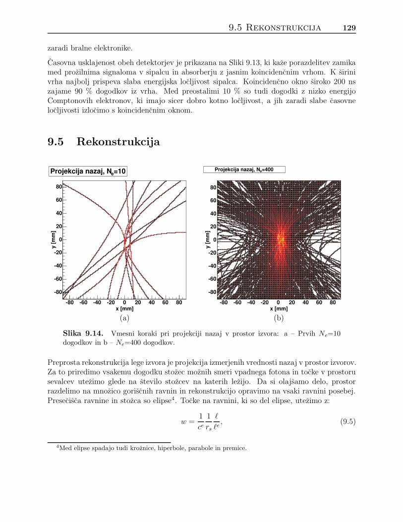
9.5 Rekonstrukcija 129
zaradi bralne elektronike.
Casovna usklajenost obeh detektorjev je prikazana na Sliki 9.13, ki kaze porazdelitev zamikamed prozilnima signaloma v sipalcu in absorberju z jasnim koincidencnim vrhom. K sirinivrha najbolj prispeva slaba energijska locljivost sipalca. Koincidencno okno siroko 200 nszajame 90 % dogodkov iz vrha. Med preostalimi 10 % so tudi dogodki z nizko energijoComptonovih elektronov, ki imajo sicer dobro kotno locljivost, a jih zaradi slabe casovnelocljivosti izlocimo s koincidencnim oknom.
9.5 Rekonstrukcija
x [mm]-80 -60 -40 -20 0 20 40 60 80
y [m
m]
-80
-60
-40
-20
0
20
40
60
80
=10eProjekcija nazaj, N
x [mm]-80 -60 -40 -20 0 20 40 60 80
y [m
m]
-80
-60
-40
-20
0
20
40
60
80
=400eProjekcija nazaj, N
(a) (b)
Slika 9.14. Vmesni koraki pri projekciji nazaj v prostor izvora: a – Prvih Ne=10dogodkov in b – Ne=400 dogodkov.
Preprosta rekonstrukcija lege izvora je projekcija izmerjenih vrednosti nazaj v prostor izvorov.Za to priredimo vsakemu dogodku stozec moznih smeri vpadnega fotona in tocke v prostorusevalcev utezimo glede na stevilo stozcev na katerih lezijo. Da si olajsamo delo, prostorrazdelimo na mnozico goriscnih ravnin in rekonstrukcijo opravimo na vsaki ravnini posebej.Presecisca ravnine in stozca so elipse4. Tocke na ravnini, ki so del elipse, utezimo z:
w =1
ce
1
rs
`
`e, (9.5)
4Med elipse spadajo tudi kroznice, hiperbole, parabole in premice.
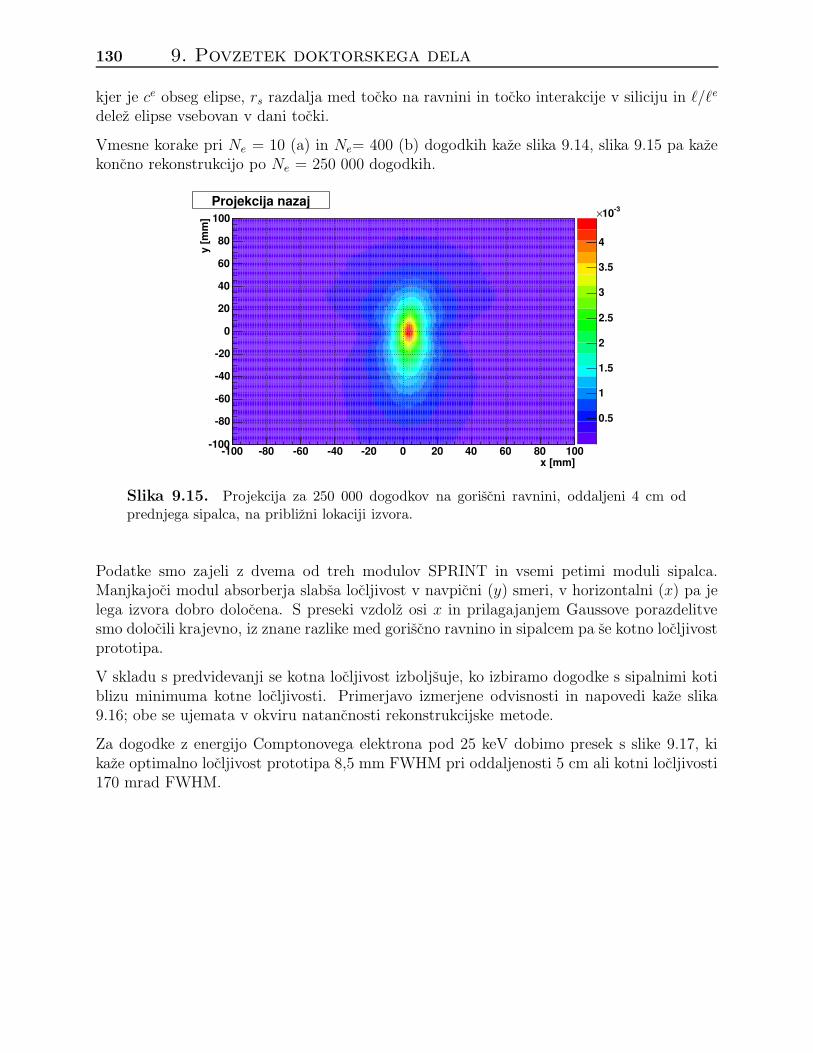
130 9. Povzetek doktorskega dela
kjer je ce obseg elipse, rs razdalja med tocko na ravnini in tocko interakcije v siliciju in `/`e
delez elipse vsebovan v dani tocki.
Vmesne korake pri Ne = 10 (a) in Ne= 400 (b) dogodkih kaze slika 9.14, slika 9.15 pa kazekoncno rekonstrukcijo po Ne = 250 000 dogodkih.
x [mm]-100 -80 -60 -40 -20 0 20 40 60 80 100
y [m
m]
-100
-80
-60
-40
-20
0
20
40
60
80
100
0.5
1
1.5
2
2.5
3
3.5
4
-310×Projekcija nazaj
Slika 9.15. Projekcija za 250 000 dogodkov na goriscni ravnini, oddaljeni 4 cm odprednjega sipalca, na priblizni lokaciji izvora.
Podatke smo zajeli z dvema od treh modulov SPRINT in vsemi petimi moduli sipalca.Manjkajoci modul absorberja slabsa locljivost v navpicni (y) smeri, v horizontalni (x) pa jelega izvora dobro dolocena. S preseki vzdolz osi x in prilagajanjem Gaussove porazdelitvesmo dolocili krajevno, iz znane razlike med goriscno ravnino in sipalcem pa se kotno locljivostprototipa.
V skladu s predvidevanji se kotna locljivost izboljsuje, ko izbiramo dogodke s sipalnimi kotiblizu minimuma kotne locljivosti. Primerjavo izmerjene odvisnosti in napovedi kaze slika9.16; obe se ujemata v okviru natancnosti rekonstrukcijske metode.
Za dogodke z energijo Comptonovega elektrona pod 25 keV dobimo presek s slike 9.17, kikaze optimalno locljivost prototipa 8,5 mm FWHM pri oddaljenosti 5 cm ali kotni locljivosti170 mrad FWHM.
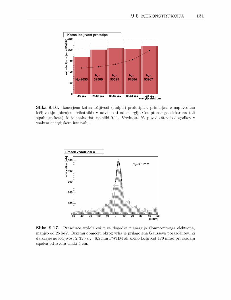
9.5 Rekonstrukcija 131
energija elektrona<25 keV 25-30 keV 30-35 keV 35-40 keV >40 keV
energija elektrona<25 keV 25-30 keV 30-35 keV 35-40 keV >40 keV
kotn
a lo
cljiv
ost [
mra
d FW
HM
]
0
50
100
150
200
250Kotna locljivost prototipa
=2655eN=eN
55025=eN
61864=eN
9396732506=eN
Slika 9.16. Izmerjena kotna locljivost (stolpci) prototipa v primerjavi z napovedanolocljivostjo (obrnjeni trikotniki) v odvisnosti od energije Comptonskega elektrona (alisipalnega kota), ki je enaka tisti na sliki 9.11. Vrednosti Ne povedo stevilo dogodkov vvsakem energijskem intervalu.
x [mm]-50 -40 -30 -20 -10 0 10 20 30 40 50
utez
cel
ice
[arb
]
0
100
200
300
400
500
Presek vzdolz osi X
=3.6 mmxσ
Slika 9.17. Presecisce vzdolz osi x za dogodke z energijo Comptonovega elektrona,manjso od 25 keV. Ozkemu obmocju okrog vrha je prilagojena Gaussova porazdelitev, kida krajevno locljivost 2, 35×σx=8,5 mm FWHM ali kotno locljivost 170 mrad pri razdaljisipalca od izvora enaki 5 cm.
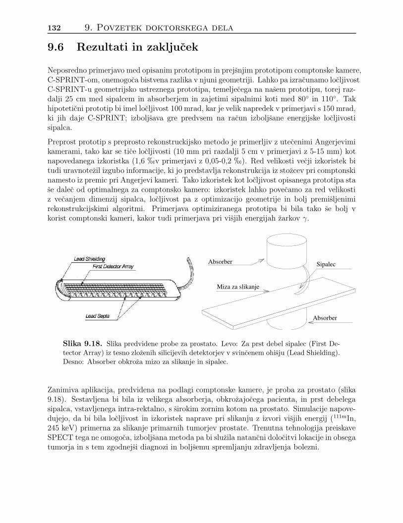
132 9. Povzetek doktorskega dela
9.6 Rezultati in zakljucek
Neposredno primerjavo med opisanim prototipom in prejsnjim prototipom comptonske kamere,C-SPRINT-om, onemogoca bistvena razlika v njuni geometriji. Lahko pa izracunamo locljivostC-SPRINT-u geometrijsko ustreznega prototipa, temeljecega na nasem prototipu, torej raz-dalji 25 cm med sipalcem in absorberjem in zajetimi sipalnimi koti med 80 in 110. Takhipoteticni prototip bi imel locljivost 100 mrad, kar je velik napredek v primerjavi s 150 mrad,ki jih daje C-SPRINT; izboljsava gre predvsem na racun izboljsane energijske locljivostisipalca.
Preprost prototip s preprosto rekonstruckijsko metodo je primerljiv z utecenimi Angerjevimikamerami, tako kar se tice locljivosti (10 mm pri razdalji 5 cm v primerjavi z 5-15 mm) kotnapovedanega izkoristka (1,6 hv primerjavi z 0,05-0,2 h). Red velikosti vecji izkoristek bitudi uravnotezil izgubo informacije, ki jo predstavlja rekonstrukcija iz stozcev pri comptonskinamesto iz premic pri Angerjevi kameri. Tako izkoristek kot locljivost opisanega prototipa stase dalec od optimalnega za comptonsko kamero: izkoristek lahko povecamo za red velikostiz vecanjem dimenzij sipalca, locljivost pa z optimizacijo geometrije in bolj premisljenimirekonstrukcijskimi algoritmi. Primerjava optimiziranega prototipa bi bila tako se bolj vkorist comptonski kameri, kakor tudi primerjava pri visjih energijah zarkov γ.
Absorber
Absorber
Sipalec
Miza za slikanje
Slika 9.18. Slika predvidene probe za prostato. Levo: Za prst debel sipalec (First De-tector Array) iz tesno zlozenih silicijevih detektorjev v svincenem ohisju (Lead Shielding).Desno: Absorber obkroza mizo za slikanje in sipalec.
Zanimiva aplikacija, predvidena na podlagi comptonske kamere, je proba za prostato (slika9.18). Sestavljena bi bila iz velikega absorberja, obkrozajocega pacienta, in prst debelegasipalca, vstavljenega intra-rektalno, s sirokim zornim kotom na prostato. Simulacije napove-dujejo, da bi bila locljivost in izkoristek naprave pri slikanju z izvori visjih energij (111mIn,245 keV) primerna za slikanje primarnih tumorjev prostate. Trenutna tehnologija preiskaveSPECT tega ne omogoca, izboljsana metoda pa bi sluzila natancni dolocitvi lokacije in obsegatumorja in s tem zgodnejsi diagnozi in boljsemu spremljanju zdravljenja bolezni.

Appendix A
Sources of electronic noise and their
propagation through front-end
electronics
C
R
C’
R
R
C
R
vout
Rp
p
u u
i
id
d
differentiator integrator
SHAPER
e
preamplifier
niisCD
SENSOR
n
Figure A.1: A schematic representation of the first stage electronics circuit and thesensor, including the noise sources.
Figure A.1 shows the electronic schematic, including the noise sources. They come in twovarieties, either as en, a voltage noise source or in, a current noise source. Both currentand voltage noise are white, i.e. independent of the frequency, and are quantified with theirspectral power densities, in terms of V 2/Hz or A2/Hz for voltage or current noise sources,respectively.
The noise at the output (vout) is the integral of N 2, the voltage spectral power density
133
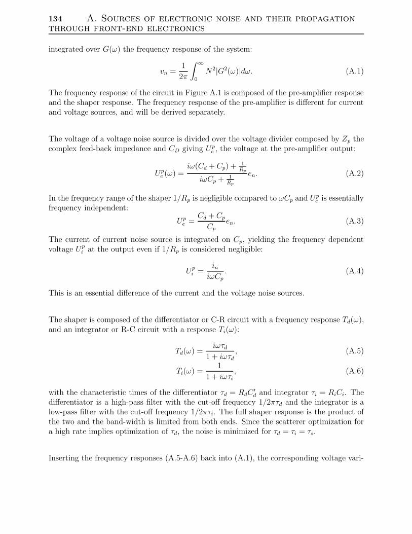
134 A. Sources of electronic noise and their propagationthrough front-end electronics
integrated over G(ω) the frequency response of the system:
vn =1
2π
∫ ∞
0
N2|G2(ω)|dω. (A.1)
The frequency response of the circuit in Figure A.1 is composed of the pre-amplifier responseand the shaper response. The frequency response of the pre-amplifier is different for currentand voltage sources, and will be derived separately.
The voltage of a voltage noise source is divided over the voltage divider composed by Zp thecomplex feed-back impedance and CD giving Up
e , the voltage at the pre-amplifier output:
Upe (ω) =
iω(Cd + Cp) + 1Rp
iωCp + 1Rp
en. (A.2)
In the frequency range of the shaper 1/Rp is negligible compared to ωCp and Upe is essentially
frequency independent:
Upe =
Cd + Cp
Cp
en. (A.3)
The current of current noise source is integrated on Cp, yielding the frequency dependentvoltage Up
i at the output even if 1/Rp is considered negligible:
Upi =
iniωCp
. (A.4)
This is an essential difference of the current and the voltage noise sources.
The shaper is composed of the differentiator or C-R circuit with a frequency response Td(ω),and an integrator or R-C circuit with a response Ti(ω):
Td(ω) =iωτd
1 + iωτd
, (A.5)
Ti(ω) =1
1 + iωτi
, (A.6)
with the characteristic times of the differentiator τd = RdC′d and integrator τi = RiCi. The
differentiator is a high-pass filter with the cut-off frequency 1/2πτd and the integrator is alow-pass filter with the cut-off frequency 1/2πτi. The full shaper response is the product ofthe two and the band-width is limited from both ends. Since the scatterer optimization fora high rate implies optimization of τd, the noise is minimized for τd = τi = τs.
Inserting the frequency responses (A.5-A.6) back into (A.1), the corresponding voltage vari-

135
ations Vi and Vv of the current and voltage noise sources are obtained:
V 2v =
e2n
τ
(Cd + Cp)2
C2p
1
2π
∫ ∞
0
ω2τ 2
(
1 + ω2τ 2)2d(ωτ), (A.7)
V 2i =
i2n τ
C2p
1
2π
∫ ∞
0
1(
1 + ω2τ 2)2d(ωτ). (A.8)
The numerical value of both integrals is π/4, and the total noise appearing at the output is:
V 2n =
1
8
(
e2n
(Cd + Cp)2
C2p
1
τ+ i2n
1
C2p
τ
)
. (A.9)

136 A. Sources of electronic noise and their propagationthrough front-end electronics

Appendix B
List-mode maximum likelihood
expectation maximization
The list-mode maximum likelihood expectation maximization (LML/EM) method is an ap-proximate reconstruction method. It consists of three combined approaches: image quality isestimated based on maximum likelihood, it is optimizied based on expectation maximizationand data is organized as a list, hence list-mode. A breif explanation of each of the termsfollows.
The maximum likelihood is translated into the imaging theory as a comparison in the mea-surement space. The interpretation is given for binned image in the measurement space.Poisson distribution of the bin content m′
j of bin j, bin index designated by values of allmeasured parameters for an event (impact positions in both sensor parts, energy measure-ment), is assumed, with the average value mj =
∑Mi=1 Tjisi given by the forward projection
of the source distribution, equation (6.3). Then the part of the logarithm of the maximumlikelihood (log-likelihood) which depends on the source distribution is given by:
log L =
M∑
j=1
m′j log(
N∑
i=1
Tjisi) −M∑
j=1
N∑
i=1
Tjisi. (B.1)
The expectation maximization is the variation of the source distribution si which maximizeslog-likelihood under the condition that all si are non-negative.
The log-likelihood as defined by (B.1) above still requires the full matrix Tji to be stored andmanipulated. This requirement is circumvented if the list-mode approach is used. since thesum in (B.1) is evaluated only for measured points. This can be interpreted as decreasing thebin size of the measurement space until each measurement corresponds to a single bin. Thenthe measured contents m′
j are either 1 if there is an event with measurements correspondingto set indexed by j or 0 for the rest of the measurement space. The remaining indices, i.e.
137
138 B. List-mode maximum likelihood expectationmaximization
those with content 1, are re-labeled to indices e which label the event, in which the set ofparameters corresponding to the bin index j were measured. This requires a re-interpretationof the matrix elements Tji calculated in the binned case - there they were used to indicatethe portion of data a source at position labeled i will give in measurement bin j. Now thematrix elements are labeled tei and signify the probability that the photon originating in iwill be detected as event e. The log-likelihood is now:
Llm(si) = −Ne∑
e=1
( N∑
i=1
teisi
)
+
Ne∑
e=1
log(
Ne∑
i=1
si), (B.2)
with Ne number of detected events.
The expectation maximization yields the iteration step:
s′ (+)i =
s′i
Ri(1 + α∑N
k=1 riks′k)
Ne∑
e=1
tei∑N
k=1 teks′k
, (B.3)
where s′(+) is the improved image estimate, and Ri is the (survival) probability that the pho-ton emitted from bin i in the image is detected anywhere in the apparatus. The denominatorof the first quotient of equation (B.3) provides a roughness penalty, with parameters α deter-mining the amount of smoothing applied. The matrix elements rik are non-negative for eightnearest neighbours relative to the pixel labeled i, and their sum is set to 0 to perserve eventcount. The roughness penalty parameter is determined for a given reconstrcution problemas α = α0/〈s′(0)〉, with 〈s′(0)〉 the average intensity of the initial image approximation s′(0),i.e. the back-projection described above. The parameter α0 nominally ranges between 0.005and 0.01.
The complexity of the reconstruction now lies with the determination of the matrix elementstei and the survival probabilities Ri as described in [WFC+01].
The relative survival probabilies are modeled assuming the absorber is homogeneous tothe extent that the probabilities Ri depend only on the first detector geometry, and areproportional to the sum:
Ri ∝∑
Vs
cos φ(1 − e−µzsi)
d2si
, (B.4)
over the cells Vs of the scatterer, with φ = 6 ~ns, (~rs − ~ri) the orientation of the face of thecell (given by the cell normal vector ~ns) with respect to the photon path, zsi the distancetraversed by the photon within the scatterer before reaching the interaction point ~rs, µ isthe total attenuation coefficient in the absorber at energy of the initial photon and dsi thedistance between the emission point ~ri and the interaction point. The assumption of theabsorber homogenity was derived for an absorber forming a full ring around the scatterermodule, and the validity of the assumption is somewhat questionable for an incomplete ring.
The relative probabilities tei that the event e was caused by a photon emitted from point
139
~ri are composed of two factors. The first factor is the probability f(e) of detecting event erelative to other collected events, and the second probability f e(i) of event being a result ofphoton emission from point ~ri relative to other points in the source space. The factors f(e)are:
f(e) ∝ e−µzsadσ
dEe, (B.5)
proportional to the probability e−µzsa that the photon escapes the scatterer with zsa thelength of path of the scattered photon in the absorber and the probability of Comptonscattering with energy transfer of Ee, which is given by the Klein-Nishina differential cross-section with respect to the energy transfer, dσ
dEe, given by equation (2.13). The factors f e(~r)
are:f e(~ri) ∝ Risg
e(~ri), (B.6)
where Ris is the summand of equation (B.4) corresponding to the scatterer cell s hit in theinteraction. In the case of perfect angular resolution, the probability ge(~ri) would give theportion of the conic determined from equation (6.6), contained in the pixel centered at ~ri
of the image. Since this is clearly not the case, there is a probability that pixels close tothose lying on the cone were the source of the detected photon. This is accounted for byfilling the adjacent pixels according to the cone spread distribution, which is determinedfrom the parameters of the setup. The widths in terms of FWHM of the distribution forvarious scattering angles θ were computed in Chapter 5 and shown on Figure 5.5. Becauseof the non-Gaussian nature of Doppler-broadening, the cone spread distribution is not wellapproximated by a single Gaussian distribution, but a 10% addition of a Gaussian with 3times the spread gives a good agreement with a modeled response [WFC+01]. Then thefactor ge(~ri) is computed as:
ge(~ri) =
∫
Vi
d~r (0.9e−r2/2σ2
+ 0.1e−r2/2(3σ)2), (B.7)
where r is the distance between the position of the source determined from back-projection(6.6) and the position ~r within the pixel i, perpendicular to the cone axis, and σ is the conespread at the focal plane, determined as the angular resolution times the distance betweenthe interaction point and the pixel being tallied.
To summarize the algorithm: The relative probabilites that photons emitted from pixel iin the image plane are calculated using (B.4) prior to event loop. Then, for each event,the relative weights f(e) are computed and stored. In each iteration, starting from theimage generated from back-projection, the pixels intersected by the cone of the event back-projection are determined. Then this pixels and nearest neighbours are tallied with relativeprobabilites ge(~ri), and the scheme is repeated for all events. After each iteration, expectationmaximization step is performed according to equation (B.3), and the improved image isobtained.

140 B. List-mode maximum likelihood expectationmaximization
Appendix C
Parameters of data runs used in the
thesis
Table C.2 gives a list of parameters which were set for data runs which appear throught thethesis. Words abbreviated in Table C.2 are described in Table C.1.
Abbreviation/Acronym DescriptionLJ Jozef Stefan Institute, Ljubljana, SloveniaAA University of Michigan, Ann Arbor, MI, USA
CERN European Organization for Nuclear Research, Geneva, SwitzerlandGND Grounded front GND pads of VATAGP3+n n adjacent channels
M1,M2,L SPRINT moduleslj3557a, lj3557b, lj3557c
lj3557f, lj3557g scatterer modulesm mbias in µAv vfp in mV
Table C.1: List of abbreviations and acronyms which appear in Table C.2.
141
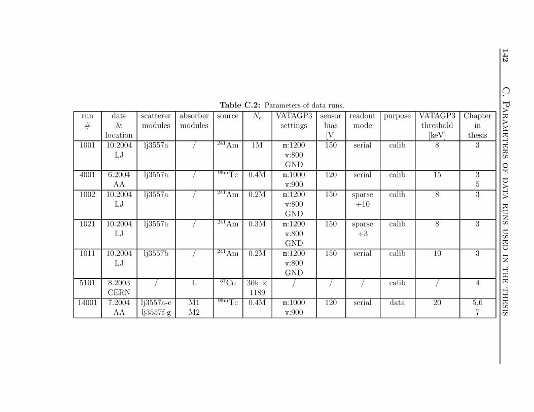
142
C.Parameters
of
data
runs
used
inthe
thesis
Table C.2: Parameters of data runs.
run date scatterer absorber source Ne VATAGP3 sensor readout purpose VATAGP3 Chapter# & modules modules settings bias mode threshold in
location [V] [keV] thesis1001 10.2004 lj3557a / 241Am 1M m:1200 150 serial calib 8 3
LJ v:800GND
4001 6.2004 lj3557a / 99mTc 0.4M m:1000 120 serial calib 15 3AA v:900 5
1002 10.2004 lj3557a / 241Am 0.2M m:1200 150 sparse calib 8 3LJ v:800 +10
GND1021 10.2004 lj3557a / 241Am 0.3M m:1200 150 sparse calib 8 3
LJ v:800 +3GND
1011 10.2004 lj3557b / 241Am 0.2M m:1200 150 serial calib 10 3LJ v:800
GND5101 8.2003 / L 57Co 30k × / / / calib / 4
CERN 118914001 7.2004 lj3557a-c M1 99mTc 0.4M m:1000 120 serial data 20 5,6
AA lj3557f-g M2 v:900 7

Appendix D
Glossary of frequently used symbols,
abbreviations and expressions
Symbol – DescriptionSPECT – single photon emission computed tomography
Compton electron – electron produced in Compton scatteringθ – scattering angle of the photon in Compton interactionc – velocity of light in vacuum 2.99×10⁸ m/s
me – electron rest mass mec2=511 keV
Eγ – energy of the initial photonEe – kinetic energy of the Compton electron~q – scattering momentum; difference of momenta of initial and
scattered photonpz – component of momentum of bound electron along the scat-
tering momentum∆~p – correction to Compton equation due to electron movement
prior to scatteringJ(pz) – distribution of pz in atom
DDKNXS – double-differential Klein-Nishina cross-sectionµ – attenuation coefficientZ – atomic numberA – atomic massσ – cross-section of interaction
NA – Avogadro number, 6.023×1026 atoms/Kmolα – Compton parameter, α = Eγ/mec
2
r0 – classical electron radius r0=2.82×10⁻¹⁵mρ – material densityd – depletion depthV – voltage drop across the diode
143

144 D. Glossary of frequently used symbols, abbreviationsand expressions
Symbol – Descriptionε – dielectric constant (for silicon ε=11.9)
ε0 – permittivity of space, ε0=8.9×10⁻¹²As/Vme0 – electron charge magnitude, e0=1.60×10⁻¹⁹As
Nd – concentration of (donor) dopants in silicon bulkVFD – full-depletion voltage
w – thickness of the sensor% – resistivity of the silicon bulkC – capacitanceS – diode area
CFD – capacitance of depleted diodeNe−h – number of created electron-hole pairs during ionization
Q – signal charge, corresponding to Ne−h electrons or holesη – average energy of fast particle required to create an electron-
hole pairie(t), ih(t) – current pulse created by moving electron/hole
qe qh – charge of charge carrier~ve(t) ~vh(t) – velocity of charge carrier
~Ew – weighting field~E – electron field
µe, µh – mobility of charge carriersx – coordinate in diode; coordinate axis traversing the sensor,
origin set at the junctionE(x) – electric field magnitude; function of xthc , tec – collection time; time necessary to collect carriers created by
ionization on the readout electrodeCp – capacitance of pre-amplifier feed-backRp – resistance of pre-amplifier feed-backτp – pre-amplifier characteristic timee – base of natural logarithm, e=2.72
vout – pulse at the output of (the slow) shaperτEs – shaping time of the slow shaper providing spectroscopic out-
putVn – noise of vout in units of voltageσn – equivalent noise charge of vout
Id – current through the diode under reverse bias conditionsea – voltage noise power density of the pre-amplifier
vthr – threshold voltage levelτ ts – shaping time of the analog pulse generating trigger
σtn – equivalent noise charge of analog pulse generating trigger
fn – rate of triggers caused by base-line oscillationsfr – maximal tolerable fn

145
Symbol – Descriptionαr – logarithmic noise rate suppression factor
Qmin – minimum detectable signal chargeEe,min – minimum energy of Compton electron required for detection
B – charge collection efficiencySINTEF – The Foundation for Scientific and Industrial Research at the
Norwegian Institute of Technology (NTH), Trondheim, Nor-way, http://www.sintef.no
ASIC – application specific integrated circuitVATAGP, VATAGP3 – chips – ASICs performing the tasks of front-end electronics
IDEAS – Ideas ASA, Snarøya, Norway,http://www.ideas.noDAC – digital-to-analog convertermbias – master bias of VATAGP chip family which sets ASIC oper-
ating parametersvfp – bias which sets Rp and consequentially τp
PCB – printed circuit boardDAQ – data acquisitionVME – physical interface and communication standard,
http://www.vita.com
IB – intermediate boardFPGA – Field-Programmable Gate Array
PC – personal computerADC – analog-to-digital converter
pi – pedestal of channel, pad indexed with ise
i – content (in units of ADC) of readout channel i in event eσi – noise of channel ice – common-mode shift of se
i in event eNc – number of channels per chipNe – number of collected events, 1/Ne is also used as pedestal
update weightFWHM – full-width at half-maximum
C0 – pre-amplifier capacitanceCL – load capacitance
RMS – root mean squarePMT – photo-multiplier tube
SPRINT – single photon ring tomographBGO – bismuth germanate
Es – energy of the scattered photonLi – amount of light collected on PMT i
NPM – number of PMTs in a module, 20gi – relative gain correction of PMT i~ri – position of PMT i centerε – detector efficiency

146 D. Glossary of frequently used symbols, abbreviationsand expressions
Symbol – Descriptiona(θ) – setup acceptance at a given scattering angle
Ω1 – solid angle of the scatterer relative to the sourceP (θ) – probability density for Compton scattering versus θ
D – distance between the source and interaction point in thescatterer
D0 – distance between the source and the scatterer~ra – interaction point in the absorber~rs – interaction point in the scatterer~r – position of the sourceR – distance between interaction points in the scatterer and ab-
sorberS(~r) – distribution of relative source intensity
y – vector of measurements, y=(~rs,Es,~ra)M(y) – distribution of measurements, measurement image
si – intensity of sources in pixel/voxel centered at ~ri, si =∫
Vid~rS(~r)
mj – event count in bin j of measurement spaceT ij – transfer matrix; probability that source placed at ~ri will
cause events in bin j of measurement spacece – circumference of conic (ellipse) on focal plane for event eris – distance between point ri on the focal plane and rs
`ei – length of conic contained in pixel i for event e
`etotal – total length of conic on focal plane in event ewe
i – weight assigned to pixel in event ewi – total weight assigned to pixel for Ne back-projected events

Bibliography
[Ang58] H. O. Anger, Scintillation camera, Rev. Sci. Instr. 29 (1958), no. 1.
[Bla99] J.W. Le Blanc, Compton camera for low energy gamma-ray imaging in nuclear
medicine applications, Ph.D. thesis, University of Michigan, 1999.
[BOA+04] D. Bhattacharyaa, T. J. O’Neilla, A. Akyuzb, J. Samimic, and A. D. Zych,Prototype tigre compton -ray balloon-borne telescope, New Astronomy Review48 (2004), 287–292.
[Com23] H. A. Compton, Phys.Rev. 22 (1923), 483.
[Fan47] U. Fano, Phys. Rev. 72 (1947), 26.
[GFD+96] F. D. Geeter, P. R. Franken, M. Defrise, H. Andries, E. Saelens, and A .Bossuyt,Optimal collimator choice for sequential iodine-123 and technetium-99m imag-
ing, Eur J Nucl Med. 7 (1996), no. 23, 768–74.
[GFF+93] N. Gehrels, C. E. Fichtel, G. J. Fishman, J. D. Kurfess, and V. Schnfelder, The
compton gamma-ray observatory, Scientific American 269 (1993), no. 6, 38–45.
[HBO+98] G. H. Hinkle, J. K. Burgers, J. O. Olsen, B. S. Williams, R. A. Lamatrice, R. F.Barth, B. Rogers, and R. T. Maguire, Prostate cancer abdominal metastases
detected with indium-111 capromab pendetide, Journal of Nuclear Medicine 39
(1998), no. 4, 650–652.
[HLS90] T. Hebert, R. Leahy, and M. Singh, Three-dimensional maximum-likelihood re-
construction for a electronically collimated single-photon-emission imaging sys-
tem, J. Opt. Soc. Am. A 7 (1990), 1305–1313.
[HVB+75] J. H. Hubbell, W. J. Veigele, E. A. Briggs, R. T. Brown, D. T. Cromer, and R. J.Howerton, Atomic form factors, incoherent scattering functions, and photon
scattering cross sections, J. Phys. Chem. Ref. Data 4 (1975), 471–538.
[KAS+04] G. Kanbach, R. Andritschke, F. Schopper, V. Schonfelder, A. Zoglauer, P. F.Bloser, S. D. Hunter, J. A. Ryan, M. McConnell, V. Reglero, G. Dicocco, andJ. Knodlseder, The MEGA project, New Astronomy Review 48 (2004), 275–280.
147

148 BIBLIOGRAPHY
[KN28] O. Klein and Y. Nishina, Zeits. fur Physik 52 (1928), 853.
[Kno99] G. F. Knoll, Radiation detection and measurement, 3 ed., John Wiley & Sons,1999.
[KWM+98] D. Kahn, R. D. Williams, M. J. Manyak, M. K. Haseman MK, D. W. Seldin, J. A.Libertino, and R. T. Maguire, 111indium-capromab pendetide in the evaluation
of patients with residual or recurrent prostate cancer after radical prostatectomy.
the prostascint study group., J Urol. 159 (1998), no. 6, 2041–2047.
[LCH+98] J.W. LeBlanc, N. H. Clinthorne, C. H. Hua, E. Nygard, W. L. Rogers, D. K.Wehe, P. Weilhammer, and S.J. Wilderman, C-sprint: A prototype compton
camera system for low energy gamma ray imaging, IEEE, Trans. Nucl. Sci. 45
(1998), 943–949.
[LCH+99] J. W. LeBlanc, N. H. Clinthorne, C. H. Hua, E. Nygard, W. L. Rogers, D. K.Wehe, P. Weilhammer, and S. J. Wilderman, Experimental results from the
c-sprint prototype compton camera, IEEE Trans. Nucl. Sci. 46 (1999), no. 3,201–4.
[LKS+02] Z. Liu, G. A. Kastis, G. D. Stevenson, H. H. Barrett, L. R. Furenlid, M. A.Kupinski, D. D. Patton, and D. W. Wilson, Quantitative analysis of acute my-
ocardial infarct in rat hearts with ischemia-reperfusion using a high-resolution
stationary spect system, J Nucl Med 43 (2002), 933–939.
[MKW+93] J. B. Martin, G. F. Knoll, D. K. Wehe, N. Dogan, V. Jordanov, and N. Petrick,A ring compton scatter camer for imaging medium energy gamma rays, IEEE,Trans. Nucl. Sci. 40 (1993), no. 4, 972–977.
[Par00] L. Parra, Reconstruction of cone-beam projections from compton scattered data,IEEE, Trans. Nucl. Sci 47 (2000), no. 4, 1543–1550.
[Ram39] S. Ramo, Currents induced by the electron motion, Proceedings of the I.R.E(1939), 584–5.
[RCS+88] W. L. Rogers, N. H. Clinthorne, L. Shao, P. Chiao, Y. Ding, J. A. Stamos, andK. F. Koral, Sprint ii, a second generation single photon ring tomograph, IEEE,Trans. Med. Imaging 7 (1988), 291 –297.
[Ric45] S. O. Rice, Mathematical analysis of the random noise, Bell Syst. Tech. Journal23,24 (1944,1945), 282,46.
[S. 01] S.J. Park S. J. Wilderman, L. Han et all, ”Experimental Setup for a Very High
Resolution Animal PET Based on Solid-state Detector”, Conference Record 2001IEEE Nucl. Sci. Symp. and Med. Imag. Conf., San Diego, Nov 4-10 (2001).

BIBLIOGRAPHY 149
[SCC+03] A. Studen, V. Cindro, N. H. Clinthorne, A. Czermak, W. Dulinski, J. Fuster,et al., Development of silicon pad detectors and readout electronics for a compton
camera, Nucl. Inst. Meth. A 501 (2003), 273–279.
[Sco73] J. H. Scofield, Theoretical photoionization cross sections from 1 to 1500 kev,Lawrence Livermore National Laboratory Rep. UCRL-51326 (1973).
[SHS73] V. Schonfelder, A. Hirner, and K. Schneider, A telescope for soft gamma ray
astronomy, Nucl. Inst. and Meth. in Phys. Res. 107 (1973), 385–394.
[Sin83] M. Singh, An electronically collimated gamma camera for single photon emission
computed tomography. part i: Theoretical considerations and design criteria,Med. Phys. 10 (1983), 421–427.
[TH03] T. Tomitami and M. Hirasawa, An analytical image reconstruction algorithm
to compensate for scattering angle broadening in compton cameras, Phys. Med.Biol. 48 (2003), 1009–1026.
[TNE74] R. W. Todd, J. M. Nightingale, and D. B. Everett, A proposed gamma-camera,Nature 251 (1974), 132.
[UM84] International Commission On Radiation Units and Measurements, Stopping
powers for electrons and positrons, ICRU Report 37 (1984).
[WFC+01] S.J. Wilderman, J. A. Fessler, N. H. Clinthorne, J. W. LeBlanc, and W. L.Rogers, Improved modeling of system response in list-mode em reconstruction of
compton scatter camera images, IEEE, Trans. Nucl. Sci. 48 (2001), no. 3, 11.
[WND+96] P. Weilhammer, E. Nygrd, W. Dulinski, A. Czermak, F. Djama, S. Gadomski,S. Roe, A. Rudge, F. Schopper, and J. Strobel, Si pad detectors”, Nucl. Instr.Meth. A 383 (1996), no. 1, 89–97.
[WP72] W.A.Reed and P.Eisenberger, Gamma-ray compton profiles of diamond, silicon,
and germanium, Physical Review B 6 (1972), no. 12, 4596–4604.
[WRKE98] S.J. Wilderman, W. L. Rogers, G. F. Knoll, and J. C. Engdahl, Fast algorithm
for list mode back-projection of compton scatter camera data, IEEE, Trans. Nucl.Sci. 45 (1998), no. 3, 957–61.
[Zha04] Lisha Zhang, Compton gamma-ray imaging probes for prostate and breast, Ph.D.thesis, University of Michigan, Biomedical Engineering, 2004.

150 BIBLIOGRAPHY

Izjavljam da sem avtor te doktorske disertacije.
Andrej Studen
Ljubljana, 27. junij 2005


![Analiza vrednotenja zalog JG v NEK[1] · diplomsko nalogo poskušali ugotoviti, katera metoda bi bila za NEK najustreznejša. Diplomsko delo je sestavljeno iz dveh delov. V prvem](https://img.pdfslide.us/doc/110x75/5e26641ea5319b638a605d88/analiza-vrednotenja-zalog-jg-v-nek1-diplomsko-nalogo-poskuali-ugotoviti-katera.jpg)