Embed Size (px)
Citation preview
DOCTORAATSPROEFSCHRIFT2009 | Faculteit Wetenschappen
www.uhasselt.be
Universiteit Hasselt | Campus DiepenbeekAgoralaan | Gebouw D | BE-3590 Diepenbeek | Belgiëtel.: +32(0)11 26 81 11
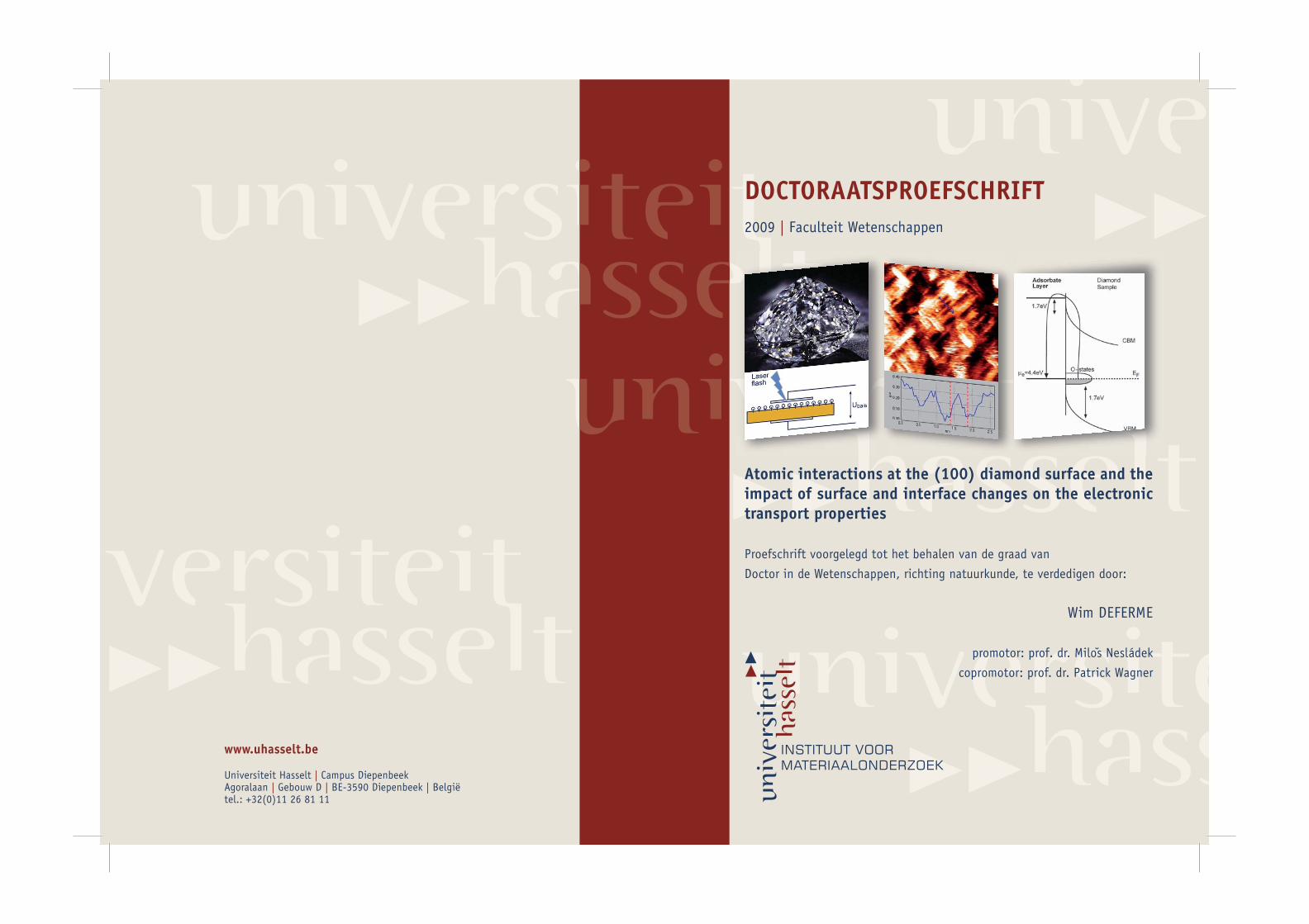
Atomic interactions at the (100) diamond surface and the impact of surface and interface changes on the electronictransport properties
Proefschrift voorgelegd tot het behalen van de graad van
Doctor in de Wetenschappen, richting natuurkunde, te verdedigen door:
Wim DEFERME
promotor: prof. dr. Milos Nesládek
copromotor: prof. dr. Patrick Wagner
˘
DOCTORAATSPROEFSCHRIFT2009 | Faculteit Wetenschappen
Atomic interactions at the (100) diamond surface and the impact of surface and interface changes on the electronictransport properties
Proefschrift voorgelegd tot het behalen van de graad van
Doctor in de Wetenschappen, richting natuurkunde, te verdedigen door:
Wim DEFERME
promotor: prof. dr. Milos Nesládek
copromotor: prof. dr. Patrick Wagner
˘
D/2009/2451/31


Chairman Prof. dr. J.V. Manca Dean Faculty of Science UHasselt, Belgium
Promotor: Prof. dr. M. Nesládek UHasselt, Belgium
Copromotor: Prof. dr. P. Wagner UHasselt, Belgium
Members of the jury: Prof. dr. K. Haenen UHasselt, Belgium Prof. dr. C. Van Haesendonck KULeuven, Belgium Dr. C.F.J. Flipse TU/e, The Netherlands Prof. dr. C. Nebel Fraunhofer Institut, Germany Prof. dr. J. Isberg Uppsala University, Sweden

Een promotor is als een vroedvrouw,
Hij moet eruit halen wat erin zit
--- Eric Henderickx ---
Acknowledgements – Dankwoord
When I started my PhD 6 years ago, one told me that a PhD is like a suspension bridge. When you are at the start of the bridge, still at the border, everything looks secure and stable. When you make progress the bridge becomes more and more unstable and once in a while some wooden boards are missing and you have to invent some “trick” to overcome this challenge. Going back a few steps to launch yourself again, in these circumstances, is a good plan. And when the bridge becomes really unstable there are always two strings, one on each side, to guide you through these difficult passages. Reaching the end, the bridge becomes more stable again but the way ahead is steep. A lot of power and courage is needed to conquer this last incline. At the end of the bridge, you can safely turn around and look back on all the obstacles you have passed along the way and armed with a lot of knowledge and experience one can continue the path. Though the path was full of obstacles there were always people to relay on and others who could give you advice on how to solve the problems.
In the first place, off course, there is Miloš. He was my guide, one of the two strings, from the start and even before. When I did my master thesis at IMO he taught me how to grow diamonds and he told me not to hurry during experiments by changing more than one parameter at the time, however sometimes changing more than one parameter at the time did work. He always came with bright ideas on how to proceed and on what to do next. After one year of PhD, Miloš decided to leave IMO for CEA, Paris. Of course, this made it more difficult for me. When having doubts about experiments, things to ask, almost everything had to go by email and it could take weeks, and reminders over and over again before Miloš did answered my mail. But in a certain way the distance between my promotor and me was also a blessing. This way I learned to solve problems myself, making mistakes but learn from those and to find my way in the community myself. And when Miloš came to IMO once in a while, we could discuss results and make plans for future work. At the end of my PhD, Miloš decided to come back to IMO which made work, especially the writing process, much easier.
ii Acknowledgements - Dankwoord
My co-promotor, Patrick Wagner, also deserves lots of gratitude. Almost every few months, when discussing my progress in my PhD-commission he had some good ideas and always asked the right questions (giving also the right answers).
A very special thanks goes to Ken. Being head of the diamond group at IMO, when Miloš left he took his time to read my articles and correct them thoroughly. Also, when writing abstracts, reaching the deadline, Ken made time to correct and rephrase them in such a way that no organizer of any meeting could reject these abstracts. When Miloš left to Paris, Ken took over part of his tasks and showed his skills of being a good “stand-in string” for my bridge.
From the people we worked together with, from our external collaborations, I especially want to thank Kees. He was my promotor for my external traineeship and for my master thesis when I was following my physics education at the Technical University of Eindhoven. During my PhD he was always there when STM measurements had to be done. Together with his Romanian student Gheorgh, we made some nice STM images and the discussions during coffee breaks or at the end of the day were very fruitful and enlightening. Kees figured out what was going on in the diamond community and helped to direct my measurements into the right direction.
From the other collaborations I would also thank Chris Van Haesendonck, Alexander Volodin and Cristina Toma from University of Leuven for the exciting collaborations and discussions.
Also Martin Van de Ven, who was always available when needed and after every PhD-meeting took a very close look to my presentations, ending up with lots of questions and useful suggestions, deserves a thanks. All those people mentioned above helped me with their propositions and discussions to overcome difficult obstacles and missing wooden boards in my bridge.
After all, I am very happy that in the beginning of my PhD I decided to choose for the 6 years assisting position rather than for the 4 years full PhD. This way I could gain some experience in teaching but also, once in a while, it is good to do something else where after a different look on the PhD subject is possible.
I express my gratitude to Gilbert Knuyt, Jean Manca, Herman Jansen and Hans-Gerd Boyen, who where the professors which I could/may assist. I thank Gilbert for guiding me through my first steps as a “teacher”, I thank Jean for his everlasting positivity related to teaching and his convincing way of lecturing. The most experience according teaching I had with Herman. As well as for the chemistry, the biology as the physics students we lectured “Golven en Optica”. Herman taught me how to keep students interested even if the subject-matter
Acknowledgements – Dankwoord iii
was too mathematical for those biology students. Hans-Gerd, at last, I would thank for helping me balance the teaching activities with the research activities.
I would like to thank my diamond colleagues at IMO: Michael, Ollie, Stoffel, Vincent, Andrada, Anna, Andrey, Didden, Paulius and Yaso. Further also Sylvia from the BIOS group deserves my gratitude because all the tips she gave me according to PhD, teaching and PhD-training in Antwerp made life more easy. Johnny, thanks for all the technical support. This short sentence can probable never express how much you mean to me and meant to my PhD. Further, also Lieven and Jan Mertens I would like to thank for their “electrical” help when needed and Jan D’Haen and Bart, thanks for all the SEM work. Christel and Hilde, thanks for the help in the analytical lab; Lea, Relinde and Marina for the sending of packages and letters; Erik for the computer problems and Dany for the pumping and safety problems.
Tenslotte zou ik ook Michel, Rik, Rene en Lucien willen bedanken voor de fijne uren in de G6. Als ik nood had aan frisse lucht, als het onderzoek even in het slop zat of als de laser het weer eens liet afweten, kon ik altijd wel terecht in de G6 voor een meer dan verse tas koffie. Met Michel bediscussieerde ik zowat alles, van het doctoreren tot het lesgeven, van het bouwen tot het trouwen, van Hattrick tot het aantal kilometers dat we liepen tijdens het weekend. Rik, merci voor de toffe heen en terugritten op de bus, voor de wijsheid over Labview, oscilloscopen en functiegeneratoren en voor de toffe babbels tussendoor. Lucien, bedankt voor de koekjes met chocolade bij de koffie en de interessante onderwerpen waarover je altijd kon doorbomen. Rene, bedankt voor de korte babbels, het klaarzetten van de labo’s “Optica en Golven” en het prepareren van experimentjes voor in de les. Bedankt, jullie maakten de tocht over de brug voor mij in elk geval niet eenzaam.
In het begin van dit dankwoord sprak ik over 2 koorden die een houvast boden tijdens het overbruggen van mijn brug, mijn doctoraat. Aan de ene kant was dat Miloš, geholpen door Ken en alle andere mensen op het IMO, aan de andere kant staan al die mensen die mij, buiten het doctoreren om, gesteund hebben.
Eerst en vooral zijn daar Sara, Bjorn, Johan en Estelle die de eerste jaren van mijn doctoraat nog bij mij op kot zaten en waarmee ik nadien, toen onze wegen zich scheidden en we elk onze eigen baan hadden, vaak tussen pot en pint over koetjes en kalfjes (of over toekans) praatte. Hopelijk blijven we, hoewel het voor ieder van ons, met het bouwen van een huisje of het stichten van een gezinnetje, drukker wordt dan ooit tevoren, op regelmatige basis met elkaar afspreken of elkaar de “Duvel” aandoen met een spelletje Risk.
Tom, uw muzikale talenten zijn waarschijnlijk groter dan uw voetbaltechnische kwaliteiten, iets wat bij mij waarschijnlijk net omgekeerd is, maar vooral uw
iv Acknowledgements - Dankwoord
interesse in wat de ander doet en uw luisterend oor op weg van en naar Achel waren (en zijn nog steeds) meer dan welkom.
Bjorn, Erik, Karen, Kim, Nele, Martha en Arno, jullie wil ik bedanken voor de alledaagse dingen. Voor de praatjes over de F1, de voetbal, reizen, … al die dingen die me de zorgen van het doctoraat even deden vergeten en me nieuwe moed gaven om er terug tegen aan te gaan, of het duimen wanneer ik een presentatie moest geven voor een overvolle zaal. Martha en Arno, bedankt om mij bij jullie een warme thuis te bezorgen en mij op te vangen met al mijn vreugde en verdriet.
Bert, mijn broerke, merci voor de steun, de discussies over fysica of wetenschap in het algemeen, waarbij ik meestal het onderspit moest delven, net zoals bij die robbertjes ravotten waar ik meestal wel enkele blauwe plekken aan overhield.
Mama en papa, merci voor jullie steun en jullie vertrouwen. Jullie hebben me gebracht tot waar ik nu sta, hebben me altijd onvoorwaardelijk gesteund, af en toe eens met wijze woorden bijgestaan, oneindig veel geduld met mij gehad maar vooral gewoon gebleven wie jullie zijn, mijn ouders waar ik ontzettend trots op ben.
En tenslotte wil ik de stevigste koord van allen bedanken voor wat ze voor mij de afgelopen 6,5 jaar heeft betekend. Een steun en toeverlaat, een luisterend oor. Het was moeilijk voor je, Inge, om altijd te begrijpen waar ik het over had maar dat maakte jou niet uit. Je luisterde vol overgave, stelde vragen of gaf me raad die me zeker heeft geholpen. En was ik op zoek van Mpumalanga tot die kaap, van ’s morgens vroeg tot ’s avonds laat. Jij, mijn suikerbossie, stond elke dag paraat.
Met dank
Wim Deferme
Diepenbeek, mei 2009
Table of contents
Acknowledgements – Dankwoord ................................................................ i
Table of contents ...................................................................................... v
Nederlandse samenvatting ........................................................................ ix
Preface .................................................................................................. 1
Chapter 1 - Introduction to diamond and its surface ..................................... 5
1.1 Diamond History ............................................................................. 5
1.2 The Diamond Structure .................................................................... 6
1.3 The Diamond Surface ...................................................................... 10
1.3.1 The (100) surface ..................................................................... 10
1.3.2 The (111) surface ..................................................................... 13
1.3.3 The (110) surface ..................................................................... 13
1.4 Diamond Doping ............................................................................ 14
1.4.1 n-type doping ........................................................................... 14
1.4.2 p-type doping ........................................................................... 14
1.4.3 Surface doping ......................................................................... 15
1.5 Properties and applications .............................................................. 23
Chapter 2 - Experimental Techniques ........................................................ 31
2.1 Deposition Systems ........................................................................ 31
2.1.1 ASTeX PDS 17 .......................................................................... 31
2.1.2 ASTeX 6500 ............................................................................. 32
2.1.3 NIRIM-type system (STS system) ................................................ 33
2.1.4 Magnetron sputtering system ..................................................... 34
vi Table of contents
2.2 Atomic Force Microscopy (AFM) ........................................................ 35
2.3 Kelvin Probe Force Microscopy (KPFM) ............................................... 38
2.4 Scanning Tunneling Microscopy/Spectroscopy (STM/STS) ..................... 39
2.5 Secondary Electron Microscopy (SEM) ............................................... 40
2.6 X-ray diffraction ............................................................................. 40
2.7 Photoelectron Spectroscopy ............................................................. 41
2.7.1 X-ray Photoelectron Spectroscopy (XPS) ...................................... 42
2.7.2 Ultraviolet Photoelectron Spectroscopy (UPS) ................................ 43
2.8 Fourier Transform IR Spectroscopy (FTIR).......................................... 43
2.9 Hall setup...................................................................................... 43
2.10 Time-of-Flight (ToF) ...................................................................... 44
2.10.1 Contact Preparation ................................................................. 44
2.10.2 Experimental Setup ................................................................. 45
2.10.3 Mobility Measurements ............................................................ 47
2.11 Rutherford Backscattering (RBS) ..................................................... 51
2.12 Elastic Recoil Detection Analysis (ERDA) .......................................... 52
Chapter 3 - Growth ................................................................................. 55
3.1 The substrate ................................................................................ 55
3.2 Growth Procedure ........................................................................... 61
3.3 Characterising the grown surface ...................................................... 65
3.4 Polycrystalline growth ..................................................................... 72
Chapter 4 - Surface Termination ............................................................... 75
4.1 Procedure ..................................................................................... 75
4.2 Characterising ............................................................................... 76
Table of contents vii
4.2.1 STM/STS measurements ............................................................ 77
4.2.2 XPS measurements ................................................................... 81
4.2.3 UPS measurements ................................................................... 83
4.2.4 KPFM measurements ................................................................. 84
4.3 Model ........................................................................................... 86
4.4 Writing on diamond ........................................................................ 89
4.5 Chlorine termination ....................................................................... 94
Chapter 5 - Time-of-Flight ..................................................................... 101
5.1 Preparation ................................................................................. 101
5.1.1 Sample.................................................................................. 102
5.1.2 Contacts ................................................................................ 102
5.1.3 Holder ................................................................................... 103
5.1.4 Set-up................................................................................... 104
5.2 Influence of laser power ................................................................ 104
5.3 Surface termination ...................................................................... 108
5.3.1 Comparison between oxidised and hydrogenated surfaces ............ 110
5.4 Temperature dependency .............................................................. 113
5.5 Contact influence ......................................................................... 117
5.6 Electroluminescence ..................................................................... 124
Chapter 6 - Conclusions and Outlook ....................................................... 129
6.1 Conclusions ................................................................................. 129
6.1.1 Ultra flat diamond growth ........................................................ 129
6.1.2 Surface characterization at the nanoscale ................................... 129
6.1.3 Transport measurements ......................................................... 130

viii Table of contents
6.2 Outlook ....................................................................................... 131
Appendix 1: List of symbols and abbreviations ................................. 135
Appendix 2: List of figures and tables ......................................... 139
Appendix 3: List of publications and presentations ........................ 145
Diamant:
alleen maar een stuk steenkool met migraine
--- L.P. Whitney ---
Nederlandse samenvatting
Diamant spreekt al eeuwen tot de verbeelding van de mens. Tot de 18de eeuw werd het enkel ontgonnen in India, daarna werd ook diamant gevonden in Brazilië en Zuid-Afrika. Diamanten waren het symbool van rijkdom en ze vormen een onderdeel van bijna alle kroonjuwelen, schatkamers en museale collecties. Ruwe diamanten worden bewerkt om hun schoonheid, en om hun hieraan verbonden waarde tot een hoogtepunt te voeren. De criteria waarmee de prijs wordt bepaald zijn de 4 c’s: cut, carat, clarity en color. Een van de bekende diamanten is de Hope diamant die in 1830 in de handel kwam en gekocht werd door de bankier H. Ph. Hope. Het is een diamant die waarschijnlijk geslepen werd uit een gestolen steen en die 45,52 karaat is.
Wanneer we het hebben over een edelsteen van een dergelijk formaat en een dergelijke kwaliteit denk je niet aan geld, maar aan de wondere eigenschappen die hem van oudsher worden toegedicht. Diamant geldt bijvoorbeeld als een symbool van zuiverheid. Onze voorvaderen controleerden de trouw van hun vrouw op de volgende wijze: ze legden een diamant onder het kussen van hun slapende gade. Als ze trouw was, wendde ze zich onmiddellijk tot haar eega en omhelsde hem, zonder wakker te worden. Als ze hem ontrouw was, wendde ze zich af en probeerde de steen op de grond te gooien. En verder geldt de diamant als een garantie voor onoverwinnelijkheid. De oude Arabieren geloofden dat bij een slag de legerleider die over de grootste diamant beschikte, zou overwinnen. Maar dat de uitzondering de regel bevestigt en dit alles met een korreltje zout moet genomen worden, bevestigde Karel de Stoute. Toen hij in de slag met de Zwitsers de reusachtige Sancy-diamant meenam behoedde hem dat niet voor de nederlaag.
Maar naast deze tot de verbeelding sprekende eigenschappen die diamant worden toegedicht is diamant ook een zeer interessant materiaal voor de industrie. Nadat aan het einde van de 18de eeuw werd ontdekt dat diamant bestaat uit koolstof, duurde het nog tot de jaren 50 van de vorige eeuw alvorens onderzoeksgroepen in Rusland, Japan en Amerika in staat waren het groeiproces van diamant te reproduceren. In eerste instantie werd diamant gegroeid op exact dezelfde manier als het ontstaat in de natuur, onder zeer hoge druk en hoge temperatuur, maar later werd ook een andere manier gevonden, de CVD-methode die toeliet om synthetisch diamant te groeien bij veel lagere drukken en temperaturen.
x Nederlandse samenvatting
In de beginjaren van het industrialisatie proces van diamant werden vooral diamantkorrels gebruikt om materialen zoals zagen, boren en beitels te harden. Diamant is namelijk het hardste materiaal dat in de natuur voorkomt en het toevoegen van diamantkorrels aan deze werktuigen leidde tot een verhoogde levensduur. Later, toen het groeiproces van diamant beter op poten stond, er atomair vlakke lagen konden afgezet worden en doperingen aan het diamant konden toegevoegd worden, verschoof de interesse in diamant zich meer naar elektronische en biologische toepassingen. Diamant is namelijk een isolator maar kan, mits dopering halfgeleidend gemaakt worden. Verder is diamant ook een uitstekende warmtegeleider wat het toepassingsgebied van diamant verder vormt. Wanneer diamant gebruikt wordt, kunnen applicaties zoals een transistor, diodes, … gevormd worden die hun toepassingsgebied hebben in hoge temperatuur, hoge frequentie en hoog vermogen elektronica.
In 1989 werd ontdekt dat het oppervlak van intrinsiek, isolerend diamant geleidend kan gemaakt worden door het hydrogeneren van het oppervlak. Het was duidelijk dat niet enkel waterstof aan het oppervlak maar ook de zo genoemde “adsorbates” op het oppervlak verantwoordelijk waren voor de geleiding. Onderzoek naar die oppervlaktegeleiding resulteerde in meer kennis over de toestand aan het oppervlak en toepassingen volgden zienderogen. Biosensoren, gebaseerd op die oppervlaktegeleiding, werden ontwikkeld en het voordeel van diamant in deze is de biocompabiliteit ervan. Het is echter nog steeds niet duidelijk wat de invloed van andere deeltjes op het mechanisme van de oppervlaktegeleiding is en daarom werd in deze thesis onderzoek verricht naar de invloed van zuurstof op de elektronische transport eigenschappen van atomair vlak diamant.
In Hoofdstuk I volgt een inleiding over diamant en het oppervlak van diamant. Het (100) georiënteerde diamant zal besproken worden en de aanhechting van waterstof en zuurstof op het oppervlak wordt van naderbij bekeken. Verder zal ook summier aandacht worden besteed aan het (111) en (110) georiënteerde oppervlak van diamant. Tenslotte zal heel uitvoerig ingegaan worden op de resultaten die in de diamant gemeenschap geboekt werden aangaande oppervlaktegeleiding. Het mechanisme wordt besproken en de recente ontwikkelingen hieromtrent worden bekeken. Als laatste in dit hoofdstuk zullen de eigenschappen van diamant en de toepassingen die hieruit voortkomen besproken worden.
In Hoofdstuk II zullen de experimentele technieken die in deze thesis worden gebruikt uitgebreid worden behandeld. Het toestel dat gebruikt wordt om onze atomaire lagen af te zetten, ASTeX, wordt in detail behandeld en de Time-of-Flight techniek die gebruikt wordt om het transport mechanisme in ons intrinsiek diamant te onderzoeken wordt toegelicht.
Nederlandse samenvatting xi
In Hoofdstuk III zullen dan de resultaten besproken worden aangaande de groei van atomair vlakke lagen diamant. De procedure van de groei zal besproken worden en het oppervlak van die lagen zal onderzocht worden met behulp van een STM (Scanning Tunneling Microscoop). Tenslotte zal ook een beetje aandacht geschonken worden aan de groei van een polikristallijnen diamant laag voor het gebruik tijdens verdere experimenten in deze thesis.
In Hoofdstuk IV wordt nader ingegaan op de oppervlakte terminatie van onze diamantlagen. De procedure van hydrogenatie wordt toegelicht, de gehydrogeneerde lagen worden gekarakteriseerd met behulp van STM, XPS (X-ray Photoelectron Spectroscopy), UPS (Ultraviolet Photoelectron Spectroscopy) en KPFM (Kelvin Probe Force Microscopy) en een model aangaande de hydrogenatie met toevoeging van zuurstof wordt opgesteld en uitgebreid bediscussieerd. Tenslotte zal er gekeken worden hoe met de AFM (Atomaire Kracht Microscoop) het oppervlak dan wel gehydrogeneerd, dan wel geoxideerd kan gemaakt worden. De terminatie van het oppervlak met chloor en amino wordt ook nog kort besproken.
Hoofdstuk V handelt volledig over de ToF (Time-of-Flight) techniek waarbij zal gekeken worden naar de invloed van oppervlakte terminatie, temperatuur en contact fabricatie op de transport eigenschappen van onze vrijstaande diamantlagen. Een model, gebaseerd op al deze metingen zal besproken worden en electro-luminescentie voortkomend uit het contact-diamant interface wordt besproken.
Tenslotte zullen in Hoofdstuk VI de resultaten behaald in de volledige thesis worden overlopen en besproken en zal er een visie worden gegeven voor metingen in de (nabije) toekomst.


As diamonds are found only in the dark depths of the earth,
Truth can only be found in the depths of the thoughts
--- Victor Hugo ---
Preface
Centuries and centuries already, diamond is a material that speaks to ones imagination. Till the 18th century it was only mined in India, after it was also found in Brazil and South-Africa. Diamonds were the symbol of richness and they were almost always part of crown jewelry, treasure houses and galleries. Rough diamonds are labored for their beauty and to raise their related value to a maximum. The criteria on which the price of diamonds is determined are the 4 c’s: cut, carat, clarity and color. One of the most famous diamonds is the Hope diamond which was introduced in business in 1830 and was bought by the banker H. Ph. Hope. It’s a diamond which has probably been polished from a stolen stone and which is 45,52 carat.
When we talk about gemstones of this format and quality it is normal that one thinks not only about money but especially about the magic properties that are traditionally given to them. Diamond is for example a symbol of purity. Our ancestors controlled the faith of the women in the following way: they placed a diamond under the pillow of the sleeping spouse. If she was faithful, she turned immediately at her husband and embraced him, without awakening. If she was unfaithful, she turned away from him and tried to throw the diamond out of the bed. And further, the diamond counts as guarantee for invincibility. In the times of the Arabs they believed that the army leader with the biggest diamond conquered. But that exceptions confirm the rule and that all of this has to be taken not to seriously, approves “Karel de Stoute”. When he took the huge Sancy-diamond with him in the battle with the Swiss, he nevertheless was defeated.
But along these fascinating properties of diamond, it is also a very interesting material for industry. After the discovery at the end of the 18th century that diamond consists of carbon, it took until the 50’s of the previous century before research groups from Russia, Japan and the USA were able to reproduce the growth process of diamond. Initially, diamond was grown in exactly the same manner as it grows in nature, at very high pressures and high temperatures. Later, it was discovered that diamond could also be grown at far lower pressures and temperatures using the so called CVD technique.
At the start of the industrializing process of diamond, diamond powder was used to harden materials like saws, drills and other tools. Diamond is namely the hardest know natural material and the addition of diamond powder to these
2 Preface
tools leads to a longer lifetime. Later, when the growth process of diamond was better established, when atomically flat layers could be grown and when the diamond could be doped, the interest in diamond shifted to more electronical and biological applications. Diamond as such is an insulator but can be made semi-conducting by doping the material with other atoms. Further, diamond is a very good heat conductor which widens the range of applications even more. By using diamond, devices like transistors, diodes … can be formed having their scope in high temperature, high frequency and high power electronics.
In 1989 it was discovered that the surface of intrinsic, insulation diamond can be made conductive by hydrogenating the surface. It was clear that not only hydrogen at the surface but also the so called “adsorbates” were responsible for this conductivity. Research for this surface conductivity resulted in more knowledge on the conditions at the surface and applications followed rapidly. Biosensors, based on this surface conductivity, were developed and the advantage of diamond is his biocompatibility. Until now it is still not completely clear what is the influence of other species on the surface conductivity and that’s why in this thesis research has been performed to check the influence of oxygen on the electronical transport properties of atomic flat diamond layers.
In Chapter I of this thesis an introduction on diamond and the surface of diamond follows. The (100) oriented diamond is discussed and the attachment of hydrogen and oxygen at the surface is looked at. Further, also the (111) and the (110) surfaces are studied briefly. At last the results achieved in the diamond community concerning surface conductivity are explored. The mechanism is discussed and the recent developments are studied. As a last part of this chapter, the properties of diamond en the application which follow from these properties are discussed.
For the use of diamond films in electronics, the properties that have the most significance are transport properties such as resistivity, carrier lifetime and mobility and thermal conductivity. In chapter 2 of this thesis the techniques used to grow and characterise the diamond layers will be explained.
In the following 3 chapters, the 3 main topics of this thesis will be discussed. Chapter 3 will be dealing very explicitly on the growth of diamond layers. The purpose of this growth is to prepare high quality diamond surfaces and to study these atomically flat layers with AFM and STM.
Chapter 4 is describing the results of the surface termination of diamond. The hydrogenation of these grown layers is studied in detail with different techniques such as XPS, UPS, STM and STS. Furthermore, the oxidised surface, prepared by a chemical or plasma treatment and the termination of the diamond surface with a mixture of hydrogen and oxygen is studied. A model will be developped and

Preface 3
the influence of different treatments on the (opto-)electrical properties will be explained. To finish this chapter other surface terminations such as chlorination will be discussed shortly.
In chapter 5, more research will study the influence of the diamond surface on some electrical properties. Time-of-Flight (ToF) is used to study the transit time and mobility of IIa free-standing single crystal diamond (100) layers. Temperature dependent measurements are performed to study the transport phenomena in freestanding diamond layers. Furthermore, the influence of contact preparation is discussed and finite light emission from the diamond-contact diodes is noticed and studied.
At last, chapter 6 will be dedicated to conclusions and some discussions together with an outlook on future work.


God created solids,
Surfaces were invented by the devil
--- W. Pauli ---
Chapter 1 - Introduction to diamond and its surface
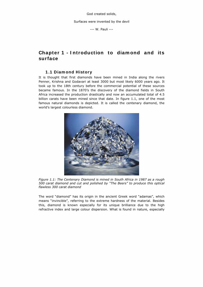
1.1 Diamond History It is thought that first diamonds have been mined in India along the rivers Penner, Krishna and Godavari at least 3000 but most likely 6000 years ago. It took up to the 18th century before the commercial potential of these sources became famous. In the 1870’s the discovery of the diamond fields in South Africa increased the production drastically and now an accumulated total of 4.5 billion carats have been mined since that date. In figure 1.1, one of the most famous natural diamonds is depicted. It is called the centenary diamond, the world’s largest colourless diamond.
Figure 1.1: The Centenary Diamond is mined in South Africa in 1987 as a rough 500 carat diamond and cut and polished by “The Beers” to produce this optical flawless 300 carat diamond
The word “diamond” has its origin in the ancient Greek word “adamas”, which means “invincible”, referring to the extreme hardness of the material. Besides this, diamond is known especially for its unique brilliance due to the high refractive index and large colour dispersion. What is found in nature, especially
6 Chapter 1 – Introduction
when it is rare, people try to copy. That’s how in the early stages of the 20th century different groups in America, Russia and Sweden tried to make diamonds synthetically, to reduce costs. But the idea of making less expensive, gem-quality diamonds synthetically is not a new one. H.G. Wells described the concept in his story “The Diamond Maker” [Wel1911] and Karl Marx commented in “Capital” that “If we could succeed, at a small expenditure of labour, in converting carbon into diamonds, their value might fall below that of bricks” [Mar1967].
After the discovery of Lavoisier and Tennant [Lav1772,Ten1797] that diamond is an allotrope of carbon, many attempts have been made to produce diamond synthetically. The first group that was able to grow a synthetic diamond according to a reproducible and verifiable process was General Electric in 1954 [Dav1994]. They were able to heat carbon to about 3000°C under a very high pressure. Later they optimised the process and the “belt” press apparatus reached pressures from 6 to 18 GPa and a temperature of 5000°C. This process was later named as the high-pressure high-temperature (HPHT) method. At the same moment Eversole et al. [Eve1962] and Bundy et al. [Bun1955] were able to develop high-pressure high-temperature (HPHT) synthetic diamonds.
Most HPHT diamonds contain nitrogen and other metallic inclusions and people tried to grow synthetically diamonds as pure as possible. Therefore, the chemical vapour deposition technique was used in the seventies to grow diamond at far lower pressures and temperatures. The first attempt was reported by Russian scientists (Deryagin, Fedoseev and Spitsyn) [Der1976, Spi1981]. Matsumoto at NIRIM used the plasma enhanced CVD technique to grow diamonds [Mat1982, Kam1983]. In the CVD technique temperatures as low as 800°C and pressures in the range of 30-500Torr are used.
Because a lot of technical and scientific problems still have to be solved, the commercialising of the synthetic diamond was not as successful as believed back in the starting days of synthetic diamond deposition.
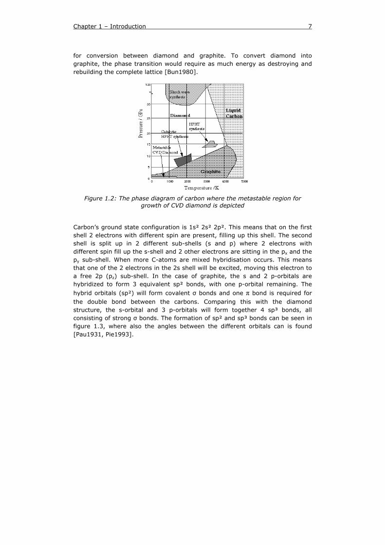
1.2 The Diamond Structure Diamond is one of the many allotropes of carbon. One of the most familiar allotropes is graphite, but also others like bucky balls, diamond-like-carbon (DLC), lonsdalite and amorphous carbon are very well known. At atmospheric pressures and temperatures graphite is the thermodynamically preferred allotrope. As can be seen in Figure 1.2 diamond is only thermodynamically stable at high temperatures and high pressures, the conditions for the natural development of diamond. At lower pressures and temperatures diamond is metastable. This means that diamond can be formed in this region and is kinetically but not thermodynamically stable due to the large activation barrier
Chapter 1 – Introduction 7
for conversion between diamond and graphite. To convert diamond into graphite, the phase transition would require as much energy as destroying and rebuilding the complete lattice [Bun1980].
Figure 1.2: The phase diagram of carbon where the metastable region for growth of CVD diamond is depicted
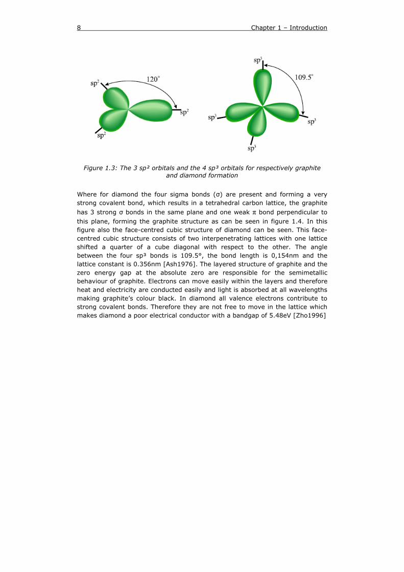
Carbon’s ground state configuration is 1s² 2s² 2p². This means that on the first shell 2 electrons with different spin are present, filling up this shell. The second shell is split up in 2 different sub-shells (s and p) where 2 electrons with different spin fill up the s-shell and 2 other electrons are sitting in the px and the py sub-shell. When more C-atoms are mixed hybridisation occurs. This means that one of the 2 electrons in the 2s shell will be excited, moving this electron to a free 2p (pz) sub-shell. In the case of graphite, the s and 2 p-orbitals are hybridized to form 3 equivalent sp² bonds, with one p-orbital remaining. The
hybrid orbitals (sp²) will form covalent σ bonds and one π bond is required for the double bond between the carbons. Comparing this with the diamond structure, the s-orbital and 3 p-orbitals will form together 4 sp³ bonds, all consisting of strong σ bonds. The formation of sp² and sp³ bonds can be seen in figure 1.3, where also the angles between the different orbitals can is found [Pau1931, Pie1993].
8 Chapter 1 – Introduction
Figure 1.3: The 3 sp² orbitals and the 4 sp³ orbitals for respectively graphite and diamond formation
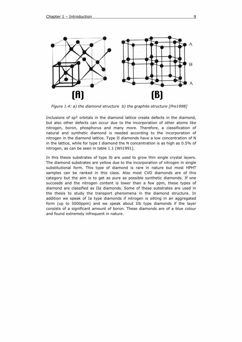
Where for diamond the four sigma bonds (σ) are present and forming a very strong covalent bond, which results in a tetrahedral carbon lattice, the graphite
has 3 strong σ bonds in the same plane and one weak π bond perpendicular to this plane, forming the graphite structure as can be seen in figure 1.4. In this figure also the face-centred cubic structure of diamond can be seen. This face-centred cubic structure consists of two interpenetrating lattices with one lattice shifted a quarter of a cube diagonal with respect to the other. The angle between the four sp³ bonds is 109.5°, the bond length is 0,154nm and the lattice constant is 0.356nm [Ash1976]. The layered structure of graphite and the zero energy gap at the absolute zero are responsible for the semimetallic behaviour of graphite. Electrons can move easily within the layers and therefore heat and electricity are conducted easily and light is absorbed at all wavelengths making graphite’s colour black. In diamond all valence electrons contribute to strong covalent bonds. Therefore they are not free to move in the lattice which makes diamond a poor electrical conductor with a bandgap of 5.48eV [Zho1996]
Chapter 1 – Introduction 9
Figure 1.4: a) the diamond structure b) the graphite structure [Pre1998]
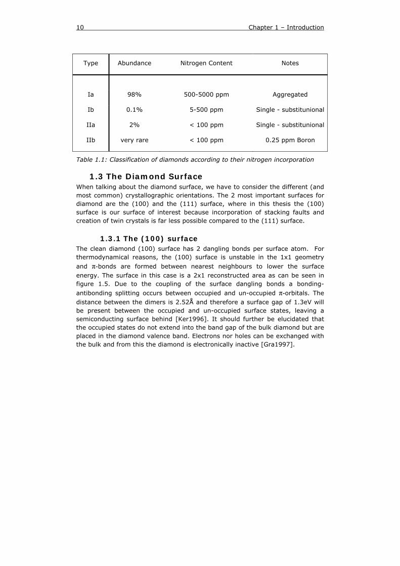
Inclusions of sp² orbitals in the diamond lattice create defects in the diamond, but also other defects can occur due to the incorporation of other atoms like nitrogen, boron, phosphorus and many more. Therefore, a classification of natural and synthetic diamond is needed according to the incorporation of nitrogen in the diamond lattice. Type II diamonds have a low concentration of N in the lattice, while for type I diamond the N concentration is as high as 0.5% of nitrogen, as can be seen in table 1.1 [Wil1991].
In this thesis substrates of type Ib are used to grow thin single crystal layers. The diamond substrates are yellow due to the incorporation of nitrogen in single substitutional form. This type of diamond is rare in nature but most HPHT samples can be ranked in this class. Also most CVD diamonds are of this category but the aim is to get as pure as possible synthetic diamonds. If one succeeds and the nitrogen content is lower than a few ppm, these types of diamond are classified as IIa diamonds. Some of these substrates are used in the thesis to study the transport phenomena in the diamond structure. In addition we speak of Ia type diamonds if nitrogen is sitting in an aggregated form (up to 5000ppm) and we speak about IIb type diamonds if the layer consists of a significant amount of boron. These diamonds are of a blue colour and found extremely infrequent in nature.
10 Chapter 1 – Introduction
Type Abundance Nitrogen Content Notes
Ia 98% 500-5000 ppm Aggregated
Ib 0.1% 5-500 ppm Single - substitunional
IIa 2% < 100 ppm Single - substitunional
IIb very rare < 100 ppm 0.25 ppm Boron
Table 1.1: Classification of diamonds according to their nitrogen incorporation
1.3 The Diamond Surface When talking about the diamond surface, we have to consider the different (and most common) crystallographic orientations. The 2 most important surfaces for diamond are the (100) and the (111) surface, where in this thesis the (100) surface is our surface of interest because incorporation of stacking faults and creation of twin crystals is far less possible compared to the (111) surface.
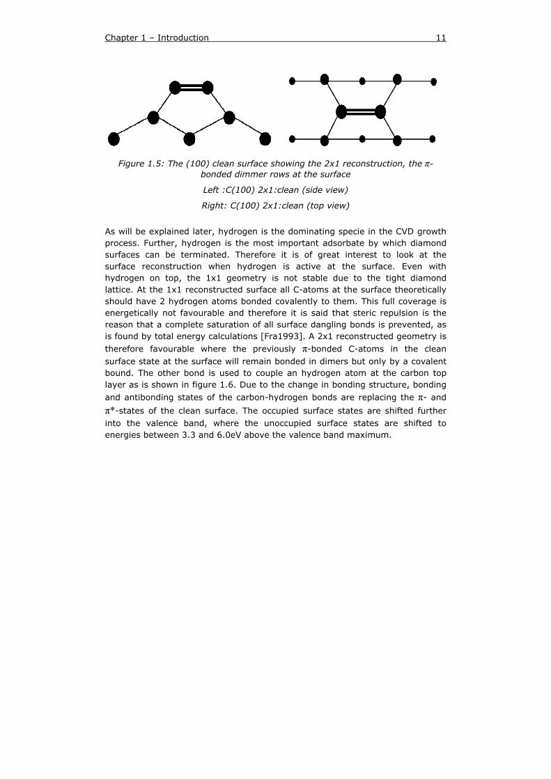
1.3.1 The (100) surface The clean diamond (100) surface has 2 dangling bonds per surface atom. For thermodynamical reasons, the (100) surface is unstable in the 1x1 geometry
and π-bonds are formed between nearest neighbours to lower the surface energy. The surface in this case is a 2x1 reconstructed area as can be seen in figure 1.5. Due to the coupling of the surface dangling bonds a bonding-
antibonding splitting occurs between occupied and un-occupied π-orbitals. The distance between the dimers is 2.52Å and therefore a surface gap of 1.3eV will be present between the occupied and un-occupied surface states, leaving a semiconducting surface behind [Ker1996]. It should further be elucidated that the occupied states do not extend into the band gap of the bulk diamond but are placed in the diamond valence band. Electrons nor holes can be exchanged with the bulk and from this the diamond is electronically inactive [Gra1997].
Chapter 1 – Introduction 11
Figure 1.5: The (100) clean surface showing the 2x1 reconstruction, the π-bonded dimmer rows at the surface
Left :C(100) 2x1:clean (side view)
Right: C(100) 2x1:clean (top view)
As will be explained later, hydrogen is the dominating specie in the CVD growth process. Further, hydrogen is the most important adsorbate by which diamond surfaces can be terminated. Therefore it is of great interest to look at the surface reconstruction when hydrogen is active at the surface. Even with hydrogen on top, the 1x1 geometry is not stable due to the tight diamond lattice. At the 1x1 reconstructed surface all C-atoms at the surface theoretically should have 2 hydrogen atoms bonded covalently to them. This full coverage is energetically not favourable and therefore it is said that steric repulsion is the reason that a complete saturation of all surface dangling bonds is prevented, as is found by total energy calculations [Fra1993]. A 2x1 reconstructed geometry is
therefore favourable where the previously π-bonded C-atoms in the clean surface state at the surface will remain bonded in dimers but only by a covalent bound. The other bond is used to couple an hydrogen atom at the carbon top layer as is shown in figure 1.6. Due to the change in bonding structure, bonding
and antibonding states of the carbon-hydrogen bonds are replacing the π- and
π*-states of the clean surface. The occupied surface states are shifted further into the valence band, where the unoccupied surface states are shifted to energies between 3.3 and 6.0eV above the valence band maximum.
12 Chapter 1 – Introduction
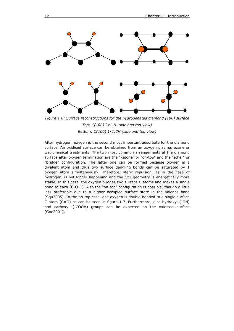
Figure 1.6: Surface reconstructions for the hydrogenated diamond (100) surface
Top: C(100) 2x1:H (side and top view)
Bottom: C(100) 1x1:2H (side and top view)
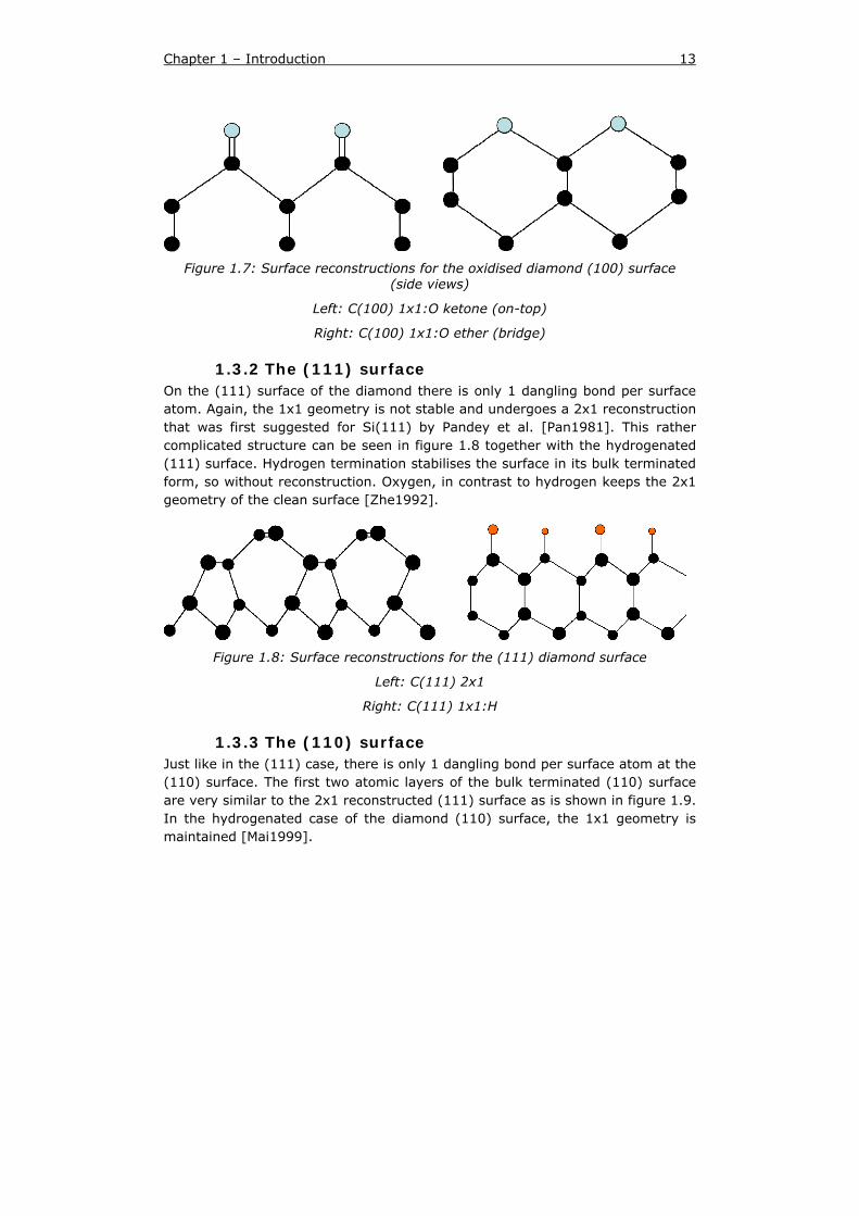
After hydrogen, oxygen is the second most important adsorbate for the diamond surface. An oxidised surface can be obtained from an oxygen plasma, ozone or wet chemical treatments. The two most common arrangements at the diamond surface after oxygen termination are the “ketone” or “on-top” and the “ether” or “bridge” configuration. The latter one can be formed because oxygen is a divalent atom and thus two surface dangling bonds can be saturated by 1 oxygen atom simultaneously. Therefore, steric repulsion, as in the case of hydrogen, is not longer happening and the 1x1 geometry is energetically more stable. In this case, the oxygen bridges two surface C atoms and makes a single bond to each (C-O-C). Also the “on-top” configuration is possible, though a little less preferable due to a higher occupied surface state in the valence band [Squ2005]. In the on-top case, one oxygen is double-bonded to a single surface C-atom (C=O) as can be seen in figure 1.7. Furthermore, also hydroxyl (-OH) and carboxyl (-COOH) groups can be expected on the oxidised surface [Goe2001].
Chapter 1 – Introduction 13
Figure 1.7: Surface reconstructions for the oxidised diamond (100) surface (side views)
Left: C(100) 1x1:O ketone (on-top)
Right: C(100) 1x1:O ether (bridge)
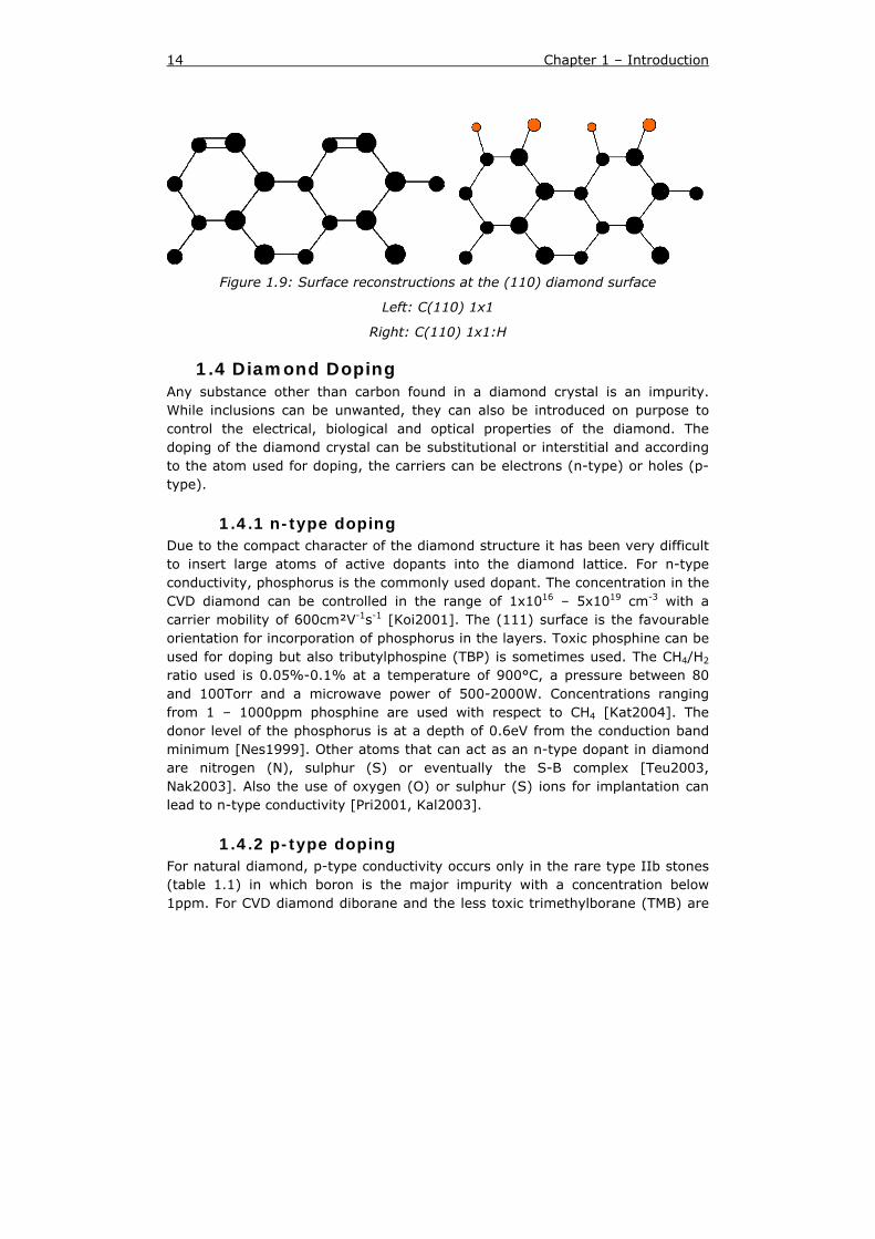
1.3.2 The (111) surface On the (111) surface of the diamond there is only 1 dangling bond per surface atom. Again, the 1x1 geometry is not stable and undergoes a 2x1 reconstruction that was first suggested for Si(111) by Pandey et al. [Pan1981]. This rather complicated structure can be seen in figure 1.8 together with the hydrogenated (111) surface. Hydrogen termination stabilises the surface in its bulk terminated form, so without reconstruction. Oxygen, in contrast to hydrogen keeps the 2x1 geometry of the clean surface [Zhe1992].
Figure 1.8: Surface reconstructions for the (111) diamond surface
Left: C(111) 2x1
Right: C(111) 1x1:H
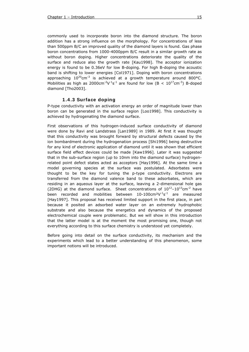
1.3.3 The (110) surface Just like in the (111) case, there is only 1 dangling bond per surface atom at the (110) surface. The first two atomic layers of the bulk terminated (110) surface are very similar to the 2x1 reconstructed (111) surface as is shown in figure 1.9. In the hydrogenated case of the diamond (110) surface, the 1x1 geometry is maintained [Mai1999].
14 Chapter 1 – Introduction
Figure 1.9: Surface reconstructions at the (110) diamond surface
Left: C(110) 1x1
Right: C(110) 1x1:H
1.4 Diamond Doping Any substance other than carbon found in a diamond crystal is an impurity. While inclusions can be unwanted, they can also be introduced on purpose to control the electrical, biological and optical properties of the diamond. The doping of the diamond crystal can be substitutional or interstitial and according to the atom used for doping, the carriers can be electrons (n-type) or holes (p-type).
1.4.1 n-type doping Due to the compact character of the diamond structure it has been very difficult to insert large atoms of active dopants into the diamond lattice. For n-type conductivity, phosphorus is the commonly used dopant. The concentration in the CVD diamond can be controlled in the range of 1x10¹⁶ – 5x1019 cm-3 with a carrier mobility of 600cm²V-1s-1 [Koi2001]. The (111) surface is the favourable orientation for incorporation of phosphorus in the layers. Toxic phosphine can be used for doping but also tributylphospine (TBP) is sometimes used. The CH4/H2 ratio used is 0.05%-0.1% at a temperature of 900°C, a pressure between 80 and 100Torr and a microwave power of 500-2000W. Concentrations ranging from 1 – 1000ppm phosphine are used with respect to CH4 [Kat2004]. The donor level of the phosphorus is at a depth of 0.6eV from the conduction band minimum [Nes1999]. Other atoms that can act as an n-type dopant in diamond are nitrogen (N), sulphur (S) or eventually the S-B complex [Teu2003, Nak2003]. Also the use of oxygen (O) or sulphur (S) ions for implantation can lead to n-type conductivity [Pri2001, Kal2003].
1.4.2 p-type doping For natural diamond, p-type conductivity occurs only in the rare type IIb stones (table 1.1) in which boron is the major impurity with a concentration below 1ppm. For CVD diamond diborane and the less toxic trimethylborane (TMB) are
Chapter 1 – Introduction 15
commonly used to incorporate boron into the diamond structure. The boron addition has a strong influence on the morphology. For concentrations of less than 500ppm B/C an improved quality of the diamond layers is found. Gas phase boron concentrations from 1000-4000ppm B/C result in a similar growth rate as without boron doping. Higher concentrations deteriorate the quality of the surface and reduce also the growth rate [Kau1998]. The acceptor ionization energy is found to be 0.36eV for low B-doping. For high B-doping the acoustic band is shifting to lower energies [Col1971]. Doping with boron concentrations approaching 1020cm-3 is achieved at a growth temperature around 800°C. Mobilities as high as 2000cm-2V-1s-1 are found for low (B < 1017cm-3) B-doped diamond [Tho2003].
1.4.3 Surface doping P-type conductivity with an activation energy an order of magnitude lower than boron can be generated in the surface region [Loo1998]. This conductivity is achieved by hydrogenating the diamond surface.
First observations of this hydrogen-induced surface conductivity of diamond were done by Ravi and Landstrass [Lan1989] in 1989. At first it was thought that this conductivity was brought forward by structural defects caused by the ion bombardment during the hydrogenation process [Shi1996] being destructive for any kind of electronic application of diamond until it was shown that efficient surface field effect devices could be made [Kaw1996]. Later it was suggested that in the sub-surface region (up to 10nm into the diamond surface) hydrogen-related point defect states acted as acceptors [Hay1996]. At the same time a model governing species at the surface was postulated. Adsorbates were thought to be the key for tuning the p-type conductivity. Electrons are transferred from the diamond valence band to these adsorbates, which are residing in an aqueous layer at the surface, leaving a 2-dimensional hole gas (2DHG) at the diamond surface. Sheet concentrations of 1012–1013cm-2 have been recorded and mobilities between 10-100cm²V-1s-1 are measured [Hay1997]. This proposal has received limited support in the first place, in part because it posited an adsorbed water layer on an extremely hydrophobic substrate and also because the energetics and dynamics of the proposed electrochemical couple were problematic. But we will show in this introduction that the latter model is at the moment the most promising one, though not everything according to this surface chemistry is understood yet completely.
Before going into detail on the surface conductivity, its mechanism and the experiments which lead to a better understanding of this phenomenon, some important notions will be introduced.
16 Chapter 1 – Introduction
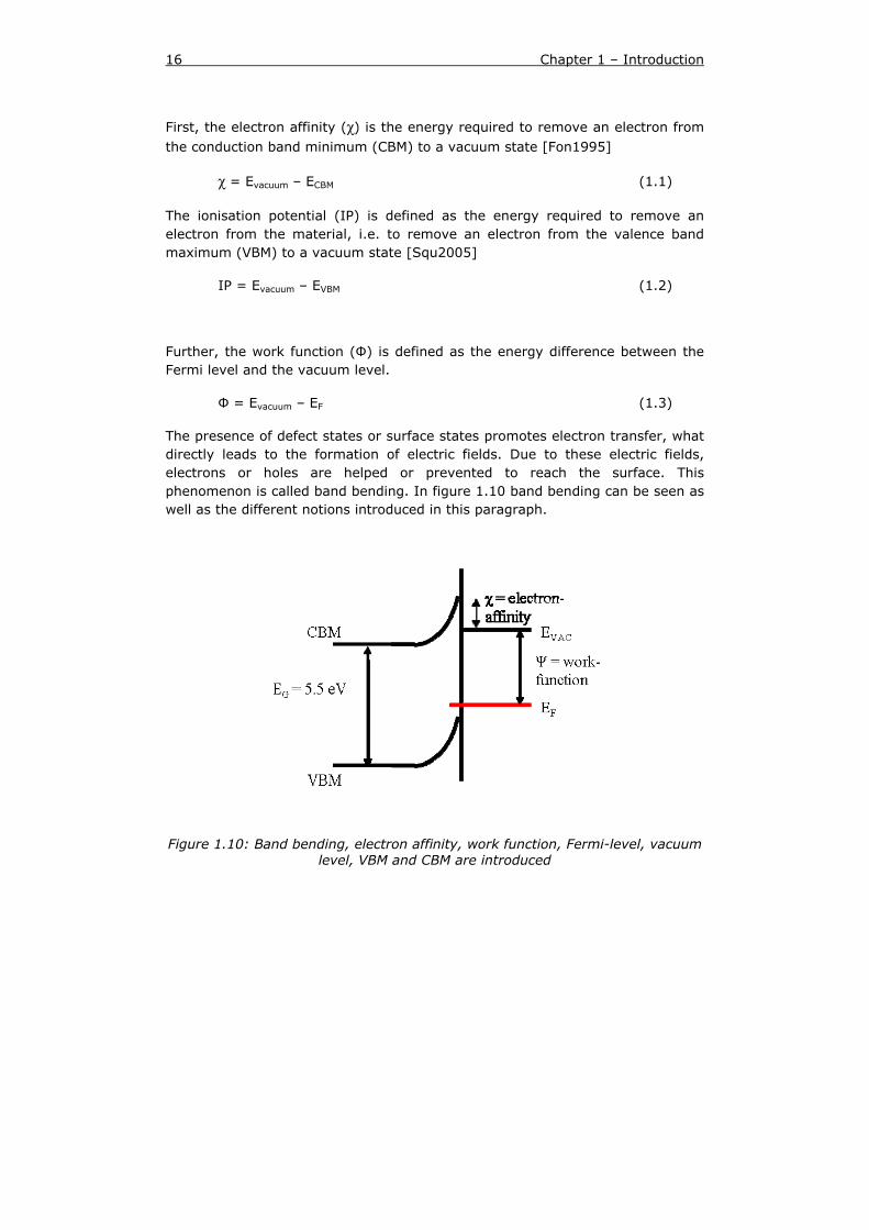
First, the electron affinity (χ) is the energy required to remove an electron from the conduction band minimum (CBM) to a vacuum state [Fon1995]
χ = Evacuum – ECBM (1.1)
The ionisation potential (IP) is defined as the energy required to remove an electron from the material, i.e. to remove an electron from the valence band maximum (VBM) to a vacuum state [Squ2005]
IP = Evacuum – EVBM (1.2)
Further, the work function (Ф) is defined as the energy difference between the Fermi level and the vacuum level.
Ф = Evacuum – EF (1.3)
The presence of defect states or surface states promotes electron transfer, what directly leads to the formation of electric fields. Due to these electric fields, electrons or holes are helped or prevented to reach the surface. This phenomenon is called band bending. In figure 1.10 band bending can be seen as well as the different notions introduced in this paragraph.
Figure 1.10: Band bending, electron affinity, work function, Fermi-level, vacuum level, VBM and CBM are introduced
Chapter 1 – Introduction 17
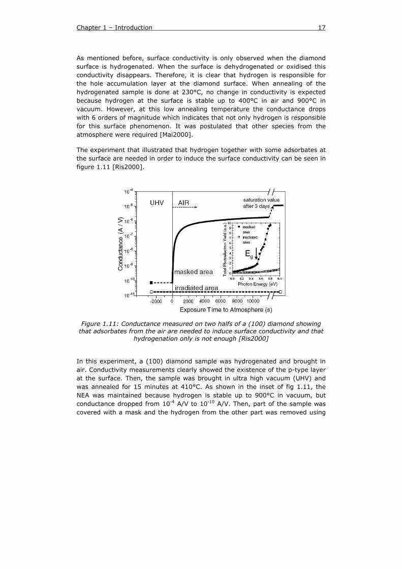
As mentioned before, surface conductivity is only observed when the diamond surface is hydrogenated. When the surface is dehydrogenated or oxidised this conductivity disappears. Therefore, it is clear that hydrogen is responsible for the hole accumulation layer at the diamond surface. When annealing of the hydrogenated sample is done at 230°C, no change in conductivity is expected because hydrogen at the surface is stable up to 400°C in air and 900°C in vacuum. However, at this low annealing temperature the conductance drops with 6 orders of magnitude which indicates that not only hydrogen is responsible for this surface phenomenon. It was postulated that other species from the atmosphere were required [Mai2000].
The experiment that illustrated that hydrogen together with some adsorbates at the surface are needed in order to induce the surface conductivity can be seen in figure 1.11 [Ris2000].
Figure 1.11: Conductance measured on two halfs of a (100) diamond showing that adsorbates from the air are needed to induce surface conductivity and that
hydrogenation only is not enough [Ris2000]
In this experiment, a (100) diamond sample was hydrogenated and brought in air. Conductivity measurements clearly showed the existence of the p-type layer at the surface. Then, the sample was brought in ultra high vacuum (UHV) and was annealed for 15 minutes at 410°C. As shown in the inset of fig 1.11, the NEA was maintained because hydrogen is stable up to 900°C in vacuum, but conductance dropped from 10-4 A/V to 10-10 A/V. Then, part of the sample was covered with a mask and the hydrogen from the other part was removed using
18 Chapter 1 – Introduction
beam-induced desorption. After this treatment, the mask was removed in-situ. As long as the sample was kept in UHV the low conductance remained. However, when the sample was brought up to air, the masked area showed an increase of 4 orders of magnitude in the first 20min and reached the same value as before the masking after 3 days. The irradiated part of the sample remained in its low conductance state with no sign of change.
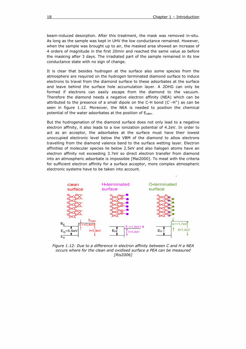
It is clear that besides hydrogen at the surface also some species from the atmosphere are required on the hydrogen terminated diamond surface to induce electrons to travel from the diamond surface to these adsorbates at the surface and leave behind the surface hole accumulation layer. A 2DHG can only be formed if electrons can easily escape from the diamond to the vacuum. Therefore the diamond needs a negative electron affinity (NEA) which can be attributed to the presence of a small dipole on the C-H bond (C-–H+) as can be seen in figure 1.12. Moreover, the NEA is needed to position the chemical potential of the water adsorbates at the position of EVBM.
But the hydrogenation of the diamond surface does not only lead to a negative electron affinity, it also leads to a low ionization potential of 4.2eV. In order to act as an acceptor, the adsorbates at the surface must have their lowest unoccupied electronic level below the VBM of the diamond to allow electrons travelling from the diamond valence band to the surface wetting layer. Electron affinities of molecular species lie below 2.5eV and also halogen atoms have an electron affinity not exceeding 3.7eV so direct electron transfer from diamond into an atmospheric adsorbate is impossible [Mai2000]. To meat with the criteria for sufficient electron affinity for a surface acceptor, more complex atmospheric electronic systems have to be taken into account.
Figure 1.12: Due to a difference in electron affinity between C and H a NEA occurs where for the clean and oxidised surface a PEA can be measured
[Ris2006]
Chapter 1 – Introduction 19
For the clean diamond surface, the band gap is 5.5eV and the electron affinity is positive (0.4eV). This means that the energy of the vacuum level is 0.4eV higher than the CBM and so, electrons cannot escape to vacuum. For the hydrogenated diamond surface, the electron affinity is, like stated before, negative (-1.3eV) because the electronegativities of hydrogen and carbon are 2.1 and 2.5 respectively. The electronegativity of oxygen is higher as that of carbon and therefore, the oxidised surface shows a positive electron affinity (PEA) of 1.7eV as also can be found in figure 1.12.
In literature, two major systems have been proposed to match the criteria for the surface conductivity. In a first approach, solvated ions within a thin water layer, provide a system that can act as a surface acceptor for diamond. Not only electrons will travel from the diamond valence band to the isolated molecular surface adsorbates, also a red/ox reaction reaching an equilibrium is included. Electrons are exchanged governing the following formula:
2H3O+ + 2e- H2 + 2H2O (1.4)
In figure 1.13 a schematic picture of the hydrogenated diamond surface in contact with a water layer is depicted. Due to the transfer of electrons the chemical potential of the water layer will change, according to Nernst’s law and to the change in pH of the aqueous layer and will move up. This transfer of electrons will go on until the chemical potential of our water layer will reach the Fermi level of our hydrogenated diamond. As a consequence, there will be a band bending of the VBM and CBM at the diamond surface as depicted in figure 1.13.

20 Chapter 1 – Introduction
Figure 1.13: In the top of this picture, the water layer with adsorbates is depicted on the hydrogenated diamond surface. At the bottom the process of electron transfer up to equilibrium is shown, ending up in an two-dimensional
hole gas at the diamond surface
In the last stage the diamond surface and the wetting layer are at equilibrium, electrons are transferred to the adsorbate layer and holes are left at the diamond surface creating a hole accumulation layer. As explained earlier, the energy difference between the chemical potential of our wetting layer and the vacuum level must be of such a level that, for spontaneous electron transfer, this potential must be below the VBM. In the case of the hydrogenated diamond, the ionisation potential was 4.2eV and thus this value can be calculated using Nernst’s equation which depends on the concentrations of [H3O
+] and [H2].
[ ] [ ]( )[ ] [ ]( ) ⎥
⎥⎦
⎤
⎢⎢⎣
⎡−=
++
SHE
SHEe HH
OHOHkT
22
233
0 //
ln2
μμ (1.5)
where μ0 = -4.44eV is the chemical potential for electrons under standard hydrogen electrode (SHE) conditions. [H3O
+]SHE and [H2]SHE are the hydronium and hydrogen concentrations of the SHE, respectively. For standard atmospheric
Chapter 1 – Introduction 21
conditions, with a pH value of 6 for the water layer, the chemical potential μe lies between -4.35 and -4.12eV such that the diamond valence band maximum falls exactly into this window.
As stated above, the hydronium/hydrogen couple is not the only which could act as surface acceptor. The second one, described by Foord [Foo2002] and Chakrapani [Cha2005] is a double red/ox couple involving the oxygen/hydroxide red/ox couple and the oxygen/ H2O couple as shown in equation 1.6a and b.
O2 + 2H2O + 4e- 4OH- (1.6a)
O2 + 4 H+ + 4e- 2H2O (1.6b)
They discuss that due to very low levels of H2 in air another mechanism than the one discussed above should be present at the diamond surface. The relatively large concentration of O2 in air-equilibrated water facilitates the reaction kinetics of equation 1.6a and 1.6b. The first red/ox couple dominates at basic conditions and the later one at acidic conditions. Using again Nernst’s equation, the chemical potential for those couples are placed at -5.66eV (pH=0) and -4.83eV (pH=14) which is far above the ionisation potential of the hydrogenated diamond of 4.2eV, so spontaneous electron transfer is possible as is shown in the inset of figure 1.15.
When UV-illumination is involved or oxygen related defect sites are created at the diamond surface also some other red/ox couples, like the ozone/oxygen one can be responsible for electron transfer [Ley2004]. The electron transfer doping will than proceed via
O3 + H2O + 2e- O2 + 2OH- (1.7)
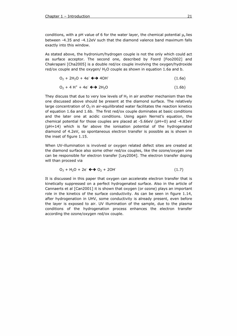
It is discussed in this paper that oxygen can accelerate electron transfer that is kinetically suppressed on a perfect hydrogenated surface. Also in the article of Cannaerts et al [Can2001] it is shown that oxygen (or ozone) plays an important role in the kinetics of the surface conductivity. As can be seen in figure 1.14, after hydrogenation in UHV, some conductivity is already present, even before the layer is exposed to air. UV illumination of the sample, due to the plasma conditions of the hydrogenation process enhances the electron transfer according the ozone/oxygen red/ox couple.
22 Chapter 1 – Introduction
Figure 1.14: Measurement of the surface conductivity during the hydrogenation process. Some high sheet conductance can already be seen during the
hydrogenation process, without exposure to air [Can2001]
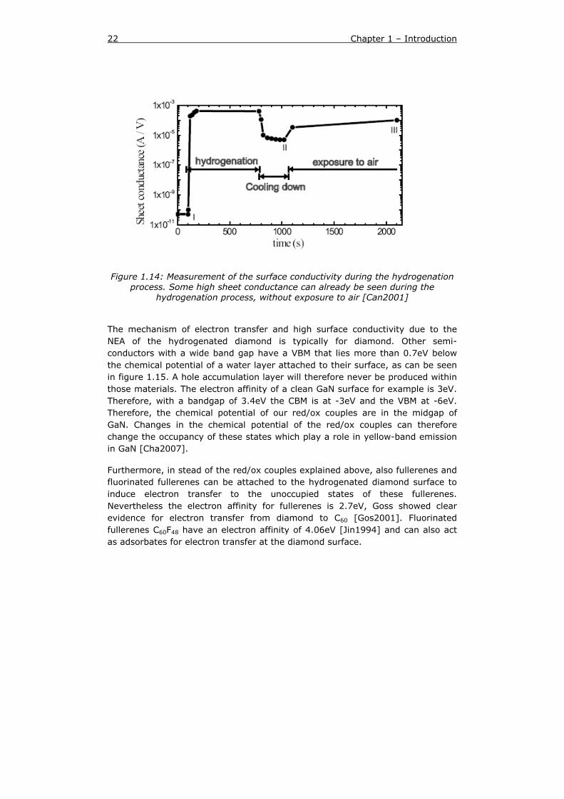
The mechanism of electron transfer and high surface conductivity due to the NEA of the hydrogenated diamond is typically for diamond. Other semi-conductors with a wide band gap have a VBM that lies more than 0.7eV below the chemical potential of a water layer attached to their surface, as can be seen in figure 1.15. A hole accumulation layer will therefore never be produced within those materials. The electron affinity of a clean GaN surface for example is 3eV. Therefore, with a bandgap of 3.4eV the CBM is at -3eV and the VBM at -6eV. Therefore, the chemical potential of our red/ox couples are in the midgap of GaN. Changes in the chemical potential of the red/ox couples can therefore change the occupancy of these states which play a role in yellow-band emission in GaN [Cha2007].
Furthermore, in stead of the red/ox couples explained above, also fullerenes and fluorinated fullerenes can be attached to the hydrogenated diamond surface to induce electron transfer to the unoccupied states of these fullerenes. Nevertheless the electron affinity for fullerenes is 2.7eV, Goss showed clear evidence for electron transfer from diamond to C60 [Gos2001]. Fluorinated fullerenes C60F48 have an electron affinity of 4.06eV [Jin1994] and can also act as adsorbates for electron transfer at the diamond surface.
Chapter 1 – Introduction 23
Figure 1.15: Band gaps of several semiconductors as well as for hydrogen-free and hydrogenated diamond. In the inset, the shift in chemical potential can be
seen as function of pH
1.5 Properties and applications Comparing the diamond structure with that of graphite, the strong covalent bonding in the diamond lattice makes this material such an interesting one for a wide gamma of applications. Not only is diamond one of the hardest materials, which makes it very useful for cutting and polishing of other materials, also its extremely good thermal conductivity at room temperature and its wide range of transparency and chemical inertness opens a complete scale of applications ranging from biological over optical to electronic ones. In table 1.2 some important properties of diamond are given and compared with those of Si and GaN, two other semiconductors. Also some related applications can be found [Gab2008, Bog2007].

24 Chapter 1 – Introduction
Properties Diamond Silicon GaN Application
Density (kg/m³) 3515 2330
Thermal Conductivity (W/m.K) 2 x 10³ 150 130
Heat Spreader, Power Electronics
Thermal Expansion Coefficient (10-6 /K) 1,1 2,6
Band Gap (eV) 5,45
(indirect) 1,1
(indirect) 3,4 High Temperature
Electronics
Electrical Resistivity (Ω.cm) 1 x 10¹³ 1 x 10³ 1 x 10⁹ Electrical Insulation
Mechanical Hardness (Gpa) 98 9,8 Cutting Tool
Index of Refraction 2,42 3,5
Electron Mobility (cm²/V.s) 2200 1500 900
Photoconductive Switches
Hole Mobility (cm²/V.s) 1800 600 150 for Pulsed Power
Applications
Breakdown Voltage (V/cm) 1 x 10⁷ 3 x 10⁵ 5 x 10⁶ Power Electronics
Saturation Velocity (m/s) 2,7 x 10⁵ 1 x 10⁵
2,7 x 10⁵
Table 1.2: Some properties of diamond as compared to Si and GaN and their related application
Focusing on the surface properties of our diamond layer, bio-electronic devices can be constructed. An hydrogen terminated diamond is conductive due to the accumulation layer. But when a small AFM tip is scanned over the surface, the surface regions where this tip has been, will be oxidised and will be insulating in stead of conductive. Also the use of photolithography and e-beam lithography can be used for local oxidation of hydrogen terminated surfaces. This oxidation
Chapter 1 – Introduction 25
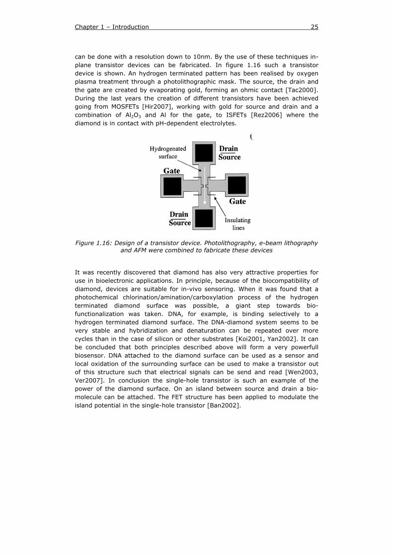
can be done with a resolution down to 10nm. By the use of these techniques in-plane transistor devices can be fabricated. In figure 1.16 such a transistor device is shown. An hydrogen terminated pattern has been realised by oxygen plasma treatment through a photolithographic mask. The source, the drain and the gate are created by evaporating gold, forming an ohmic contact [Tac2000]. During the last years the creation of different transistors have been achieved going from MOSFETs [Hir2007], working with gold for source and drain and a combination of Al2O3 and Al for the gate, to ISFETs [Rez2006] where the diamond is in contact with pH-dependent electrolytes.
Figure 1.16: Design of a transistor device. Photolithography, e-beam lithography and AFM were combined to fabricate these devices
It was recently discovered that diamond has also very attractive properties for use in bioelectronic applications. In principle, because of the biocompatibility of diamond, devices are suitable for in-vivo sensoring. When it was found that a photochemical chlorination/amination/carboxylation process of the hydrogen terminated diamond surface was possible, a giant step towards bio-functionalization was taken. DNA, for example, is binding selectively to a hydrogen terminated diamond surface. The DNA-diamond system seems to be very stable and hybridization and denaturation can be repeated over more cycles than in the case of silicon or other substrates [Koi2001, Yan2002]. It can be concluded that both principles described above will form a very powerfull biosensor. DNA attached to the diamond surface can be used as a sensor and local oxidation of the surrounding surface can be used to make a transistor out of this structure such that electrical signals can be send and read [Wen2003, Ver2007]. In conclusion the single-hole transistor is such an example of the power of the diamond surface. On an island between source and drain a bio-molecule can be attached. The FET structure has been applied to modulate the island potential in the single-hole transistor [Ban2002].
26 Chapter 1 – Introduction
Bibliography [Ash1976] Ashcroft, N.W. and Mermin, N.D. (1976), Solid State Physics, Harcourt College, Orlando
[Ban2002] Banno, T., Tachiki, M., Seo, H., Umezawa, H. and Kawarada, H. (2002) Diamond and Related Materials 11: 387
[Bog2007] Thesis Anna Bogdan, Growth and Properties of Nearly Atomically-Flat Single Crystal Diamond Prepared by Plasma-Enhanced Chemical Vapor Deposition and its Surface Interactions (2007)
[Bun1955] Bundy, F.P., Hall H.T., Strong, H.M. and Wentorf, R.H. (1955), “Man-Made Diamonds.” Nature 176 (4471): 51-55
[Bun1980] Bundy, F.P. (1980), Journal of Geophysical Research 85 (B12): 6930
[Can2001] Cannaerts, M., Nesladek, M., Haenen, K., De Schepper, L., Maslova, N.M. and Van Haesendonck, C. (2001) Physicalia 23
[Can2001] Cannaerts, M., Nesladek, M., Haenen, K., De Schepper, L., Van Haesendonck, C., Phys. Stat. Sol. (a) 186 (2001) 235
[Cha2005] Chakrapani, V., Eaton, S.C., Anderson, A.B., Tabib-Azar, M. and Angus, J.C. (2005) Electrochemical Solid-State Letters 8 E4
[Cha2007] Chakrapani, V., Angus, J.C., Anderson, A.B., Wolter, S.D., Stoner, B.R. and Sumanasekera, G.U. (2007) Science 318 : 1424
[Col1971] Collins, A. and Williams, A.W.S. (1971) Journal of Physics C: Solid State Physics 4: 1789
[Dav1994] Davidson, J.L., Spear, K.E. and Dismukes, J.P. (1994), Synthetic Diamond: Emerging Science and Technologie, John Wiley, New York, USA
[Der1976] Deryagin, B.V., Spitsyn, B.V., Builov, L.L., Klochov, A.A., Gorodetskii, A.E. and Smol’yanimov, A.V. (1976) Dokl. Akad. Nauk. SSSR 231: 333
[Eve1962] Eversol, W.G. (1962) Synthesis of Diamond, United States, Union Carbide Corp U.S. Patent 3030187 and 3030188
[Fon1995] Fong, C.Y., Klein, B.M., Diamond: electronic properties and applications, Eds.: Pan, L.S., Kania, D.R., Kluwer: Boston (1995)
[Foo2002] Foord, J.S., Lay, C.H., Hiramatsu, M., Jackman, R.B., Nebel, C.E. and Bergonzo, P. (2002) Diamond and Related Materials 11: 856
Chapter 1 – Introduction 27
[Fra1993] Frauenheim, T. (1993) Physical Review B 48: 18189
[Gab2008] Thesis Markus Gabrysch, Electronic Properties of Diamond (2008)
[Goe2001] Goeting, C.H., Marken, F., Osborn, A.R., Compton, R.G. and Foord, J.S. (2001) Electrochemical Solid State Letters 4: E29
[Gos2001] Goss, J.P., Hourahine, B., Jones, R., Heggie, M.I. and Briddon, P.R. (2001) Journal of Physics : Condensed Matter 13 : 8973
[Gra1997] Graupner, R., Hollering, M., Ziegler, A., Ristein, J., Ley, L. and Stampfl, A. (1997) Physical Review B 55: 10841
[Hay1996] Hayashi, K., Yamanaka, S., Okushi, H., Kajimura, K., Appl. Phys. Lett. 68 (1996) 376
[Hay1997] Hayashi, K., Yamanaka, S., Watanabe, H., Sekiguchi, T., Okushi, H. and Kajimura, K. (1997) Journal of Applied Physics 81: 744
[Hir2007] Hirama, K., Takayanagi, H., Yamauchi, S., Yang, J.H., Kawarade, H. and Umezawa, H. (2008) Applied Physics Letters 92, 112107
[Jin1994] Jin, C., Hettich, R.L., Compton, R.N., Tuinman, A., Derecskei-Kovacs, A., Marynick, D.S. and Dunlap, B.I. (1994) Physics Review Letters 73: 2821
[Kal2003] Kalish, R., Saguy, C., Walker, R. and Prawer, S. (2003) Journal of Applied Physics 94: 3923
[Kam1983] Kamo, M., Sato, Y., Matsumoto, S. And Setaka, N.J. (1983), Journal of Crystal Growth 62: 642
[Kat2004] Kato, H., Futako, W., Yamasaki, S. and Okushi, H. (2004) Diamond and Related Materials 13: 2117
[Kau1998] Kaukonen, M., Sitch, P.K., Jungnickel, G., Nieminen, R.M., Poykkko, S., Porezag, D. and Frauenheim, T. (1998) Physical Review B 57: 9965
[Kaw1996] Kawarada, H., Surface Science Reports 26 (1996) 205
[Ker1996] Kern, G., Hafner, J., Furthmuller, J. and Kresse, G. (1996) Surface Science 352-354: 745
[Koi2001] Koizumi, S., Watanabe, K., Hasegawa, M. and Kanda, H. (2001) Science 292: 1899
[Lan1989] Landstrass, M.I., Ravi, K.V., Appl. Phys. Lett. 55-10 (1989), 975
28 Chapter 1 – Introduction
[Lav1772] Lavoisier, A.L. (1772), Sur la destruction du diamant par le feu
[Ley2004] Ley, L., Ristein, J., Meier, F., Riedel, M. and Strobel, P. (2006) Physica B 376-377: 262
[Loo1998] Looi, H.J., Jackman, R.B. and Foord, J.S. (1998) Applied Physical Letters 72: 353
[Mai1999] Maier, F., Graupner, R., Hollering, M., Hammer, L., Ristein, L. and Ley, L. (1999) Surface Science 443 : 177
[Mai2000] Maier, F., Riedel, M., Mantel, B., Ristein, J. And Ley, L. (2000) Physical Review Letters 85 : 3472
[Mar1967] Karl Marx “Capital” Vol I (1967)
[Mat1982] Matsumoto, S., Sato, Y., Kamo, M. and Setaka, N.J. (1982), Journal of Applied Physics 21: 183
[Nak2003] Nakazawa, K., Tachiki, M., Kawarada, H., Kawamura, A. Horiuchi, K. and Ishikura, T. (2003) Applied Physical Letters 82: 2074
[Nes1999] Nesladek, M., Meykens, K., Haenen, K., Stals, L.M., Teraji, T. and Koizumi, S. (1999) Physical Review B 59: 14852
[Pan1981] Pandey, K.C. (1981) Physical Review Letters 47: 1913
[Pau1931] L. Pauling, (1931), Journal of the American Chemical Society 53: 1367
[Pie1993] Pierson, H.O. (1993), Handbook of carbon, graphite, diamond and fullerenes, Noyes Publications, New Jersey, USA
[Pre1998] Prelas, M.A., Popovici, G. and Bigelow, L.K. (1998), Handbook of industrial diamonds and diamond films, Marcel Dekker Inc, New York, USA
[Pri2001] Prins, J. (2001) Diamond and Related Materials 10: 1756
[Rez2006] Rezek, B., Garrido, J.A., Stutzmann, M., Nebel, C.E., Snidero, E. and Bergonzo, P. (2006) Physica Status Solidi (a) 193: 523
[Ris2000] Ristein, J., Maier, F., Riedel, M., Cui, J.B., Ley, L., Phys. Stat. Sol. (a) 181 (2000) 65
[Ris2006] Ristein, J. (2006) Surface Science 600 : 3677
Chapter 1 – Introduction 29
[Shi1996] Shintani, Y., J. Mater. Res. 11 (1996) 2955
[Spi1981] Spitsyn, B.V., Bouilov, L.L and Derjaguin, B.V. (1981), Vapor growth of diamond on diamond and other surfaces, Journal of Crystal Growth 52 (Part1): 219-226
[Squ2005] Sque, S.J., Jones, R. and Briddon, P.R. (2005) Physica Status Solidi (a) 202: 2091
[Tac2000] Tachiki, M., Fuduka, T., Sugata, K., Seo, H., Umezawa, H. and Kawarada, H. (2000) Japanese Journal of Applied Physics 39: 4631
[Ten1797] Tennant, S. (1797), On the nature of the diamond, Philosophical transactions of the royal society of London 87: 123-127
[Teu2003] Teukam, Z. (2003) Nature Materials 2: 482
[Tho2003] Thonke, K. (2003) Semiconductor Science and Technology 18: S20
[Ver2007] Vermeeren, V., Bijnens, N., Wenmackers, S., Daenen, M., Haenen, K., Williams, O.A., Ameloot, M., vandeVen, M., Wagner, P., Michiels, L., Langmuir 23 (2007) 26
[Wel1911] “The Diamond Maker” Project Gutenberg
[Wen2003] Wenmackers, S., Haenen, K., Nesladek, M., Wagner, P., Michiels, L., vandeVen, M., Ameloot, M., Phys. Stat. Sol. (a) 199 (2003) 44
[Wil1991] Wilks, J. and Wilks, E. (1991), Properties and Applications of Diamond, Butterworth –Heinemann, Oxford, UK
[Yan2002] Yang, W., Auciello, O., Butler, J.E., Cai, W., Carlisle, J.A., Gerbi, J.E., Gruen, D.M., Knickerbocker, T., Lasseter, T.L., Russel, J.N., Smith, L.M. and Hamers, R.J. (2002) Nature Materials 1: 253
[Zhe1992] Zheng, X.M. and Smith, P.V. (1992) Surface Science 262: 219
[Zho1996] Zhou, X., Watkis, G.D., McNamara Rutledge, K.M., Messmer, R.P. and Chawla, S. (1996), Physical Review B 54: 7881

During an experiment,
Every mistake is as instructive and valuable as success
--- Frederik van Eeden ---
Chapter 2 - Experimental Techniques
2.1 Deposition Systems Four different plasma systems have been utilized in this work. The growth of high purity, undoped single crystal (100) oriented diamond was performed in an ASTeX PDS 17 system which has a deposition chamber that is much smaller compared to the other systems and has a very low background pressure of residual gas impurities. The plasma created in this system is smaller and therefore this kind of system is perfectly suited for growth on small (3 by 3mm) HPHT diamond samples. The growth of a polycrystalline sample has been performed in an ASTeX 6500 deposition chamber. The deposition chamber in this kind of reactor is much bigger and is suited for growth on larger substrates such as 3 inch silicon wafers. Also the hydrogenation is performed in such a system. A last system which was used to functionalise the surface with chlorine and amino is a home build NIRIM-type deposition system. At last, also a magnetron sputtering system used to sputter the contacts on freestanding diamond layers will be explained in this chapter.
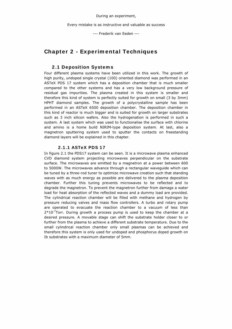
2.1.1 ASTeX PDS 17 In figure 2.1 the PDS17 system can be seen. It is a microwave plasma enhanced CVD diamond system projecting microwaves perpendicular on the substrate surface. The microwaves are emitted by a magnetron at a power between 600 to 5000W. The microwaves advance through a rectangular waveguide which can be tuned by a three-rod tuner to optimize microwave creation such that standing waves with as much energy as possible are delivered to the plasma deposition chamber. Further this tuning prevents microwaves to be reflected and to degrade the magnetron. To prevent the magnetron further from damage a water load for heat absorption of the reflected waves and a dummy load are provided. The cylindrical reaction chamber will be filled with methane and hydrogen by pressure reducing valves and mass flow controllers. A turbo and rotary pump are operated to evacuate the reaction chamber to a vacuum of less than 2*10-7Torr. During growth a process pump is used to keep the chamber at a desired pressure. A movable stage can shift the substrate holder closer to or further from the plasma to achieve a different substrate temperature. Due to the small cylindrical reaction chamber only small plasmas can be achieved and therefore this system is only used for undoped and phosphorus doped growth on Ib substrates with a maximum diameter of 5mm.
32 Chapter 2 – Experimental Techniques
Figure 2.1: The 5kW plasma enhanced microwave CVD system (ASTeX PDS17)
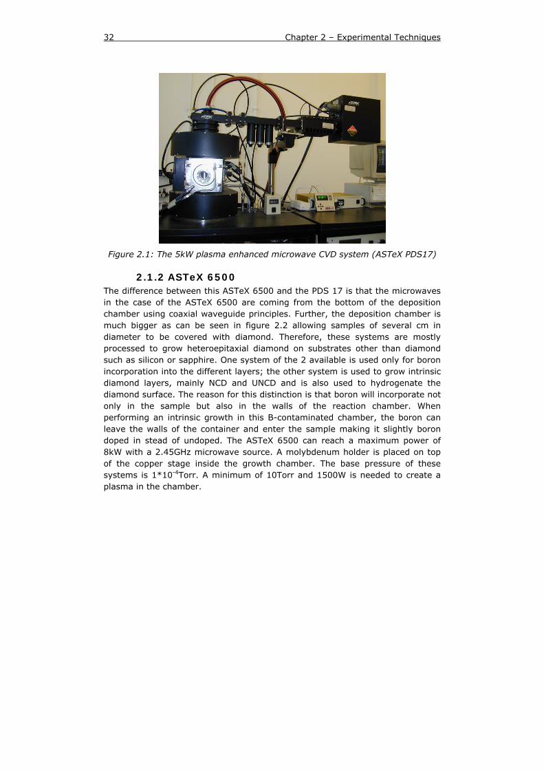
2.1.2 ASTeX 6500 The difference between this ASTeX 6500 and the PDS 17 is that the microwaves in the case of the ASTeX 6500 are coming from the bottom of the deposition chamber using coaxial waveguide principles. Further, the deposition chamber is much bigger as can be seen in figure 2.2 allowing samples of several cm in diameter to be covered with diamond. Therefore, these systems are mostly processed to grow heteroepitaxial diamond on substrates other than diamond such as silicon or sapphire. One system of the 2 available is used only for boron incorporation into the different layers; the other system is used to grow intrinsic diamond layers, mainly NCD and UNCD and is also used to hydrogenate the diamond surface. The reason for this distinction is that boron will incorporate not only in the sample but also in the walls of the reaction chamber. When performing an intrinsic growth in this B-contaminated chamber, the boron can leave the walls of the container and enter the sample making it slightly boron doped in stead of undoped. The ASTeX 6500 can reach a maximum power of 8kW with a 2.45GHz microwave source. A molybdenum holder is placed on top of the copper stage inside the growth chamber. The base pressure of these systems is 1*10-4Torr. A minimum of 10Torr and 1500W is needed to create a plasma in the chamber.
Chapter 2 – Experimental Techniques 33
Figure 2.2: The ASTeX 6500 system
2.1.3 NIRIM-type system (STS system) In this kind of MW configuration the microwaves created from the magnetron are directly passing through a quartz vacuum tube. This tube extends into the deposition chamber. As is the case for the PDS17 system also here the microwaves are tuned by a three rod tuner as shown in figure 2.3. A turbo pump is connected directly to the vacuum chamber making this system more vacuum stable. The base pressure of this system is 5*10-8Torr. A heater is installed around the vacuum chamber to bake the system such that a better vacuum is achieved. The holder is introduced from the bottom inside the quartz tube. Because of the small diameter of this quartz tube one has to be careful not to touch the walls of the tube when lightning a plasma, otherwise an inclusion of silicon as impurity will be found as will be shown later in chapter 4. Therefore only small samples are able to be grown on and functionalised. In this work, termination of chlorine and amino is performed by this system giving it the name surface treatment system (STS system).
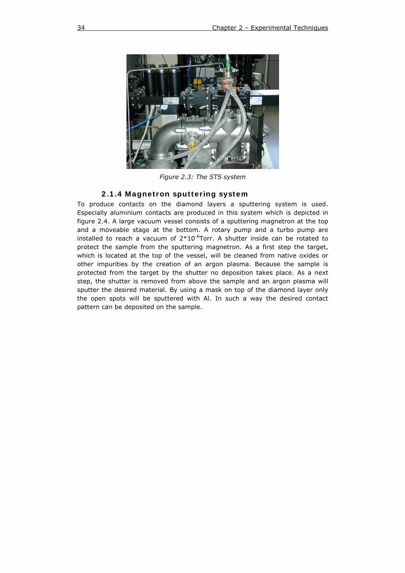
34 Chapter 2 – Experimental Techniques
Figure 2.3: The STS system
2.1.4 Magnetron sputtering system To produce contacts on the diamond layers a sputtering system is used. Especially aluminium contacts are produced in this system which is depicted in figure 2.4. A large vacuum vessel consists of a sputtering magnetron at the top and a moveable stage at the bottom. A rotary pump and a turbo pump are installed to reach a vacuum of 2*10-6Torr. A shutter inside can be rotated to protect the sample from the sputtering magnetron. As a first step the target, which is located at the top of the vessel, will be cleaned from native oxides or other impurities by the creation of an argon plasma. Because the sample is protected from the target by the shutter no deposition takes place. As a next step, the shutter is removed from above the sample and an argon plasma will sputter the desired material. By using a mask on top of the diamond layer only the open spots will be sputtered with Al. In such a way the desired contact pattern can be deposited on the sample.
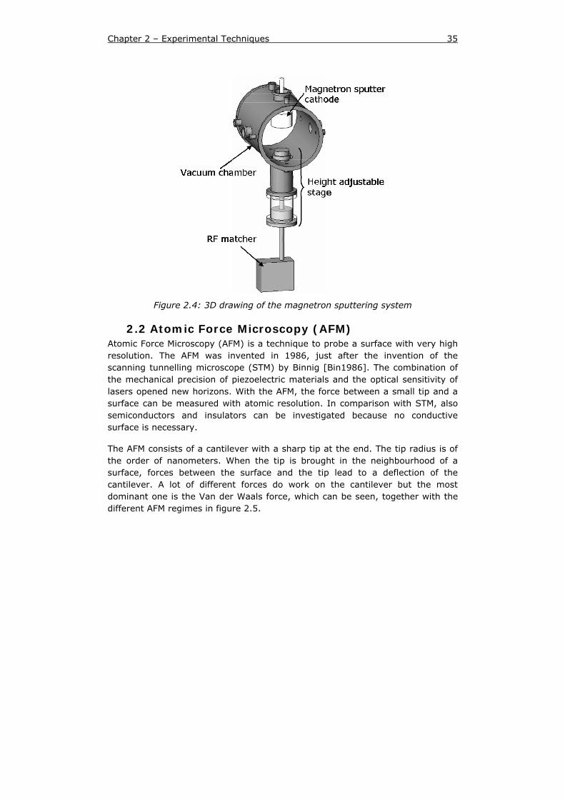
Chapter 2 – Experimental Techniques 35
Figure 2.4: 3D drawing of the magnetron sputtering system
2.2 Atomic Force Microscopy (AFM) Atomic Force Microscopy (AFM) is a technique to probe a surface with very high resolution. The AFM was invented in 1986, just after the invention of the scanning tunnelling microscope (STM) by Binnig [Bin1986]. The combination of the mechanical precision of piezoelectric materials and the optical sensitivity of lasers opened new horizons. With the AFM, the force between a small tip and a surface can be measured with atomic resolution. In comparison with STM, also semiconductors and insulators can be investigated because no conductive surface is necessary.
The AFM consists of a cantilever with a sharp tip at the end. The tip radius is of the order of nanometers. When the tip is brought in the neighbourhood of a surface, forces between the surface and the tip lead to a deflection of the cantilever. A lot of different forces do work on the cantilever but the most dominant one is the Van der Waals force, which can be seen, together with the different AFM regimes in figure 2.5.
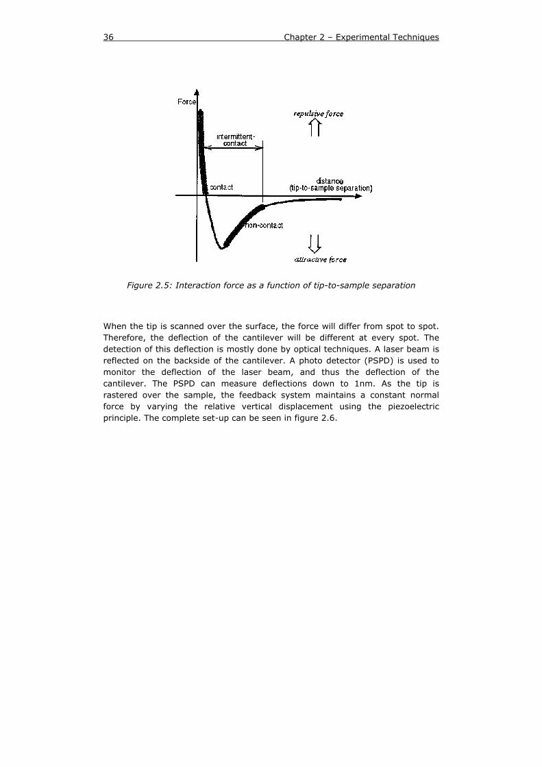
36 Chapter 2 – Experimental Techniques
Figure 2.5: Interaction force as a function of tip-to-sample separation
When the tip is scanned over the surface, the force will differ from spot to spot. Therefore, the deflection of the cantilever will be different at every spot. The detection of this deflection is mostly done by optical techniques. A laser beam is reflected on the backside of the cantilever. A photo detector (PSPD) is used to monitor the deflection of the laser beam, and thus the deflection of the cantilever. The PSPD can measure deflections down to 1nm. As the tip is rastered over the sample, the feedback system maintains a constant normal force by varying the relative vertical displacement using the piezoelectric principle. The complete set-up can be seen in figure 2.6.
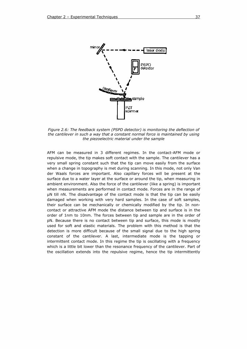
Chapter 2 – Experimental Techniques 37
Figure 2.6: The feedback system (PSPD detector) is monitoring the deflection of the cantilever in such a way that a constant normal force is maintained by using
the piezoelectric material under the sample
AFM can be measured in 3 different regimes. In the contact-AFM mode or repulsive mode, the tip makes soft contact with the sample. The cantilever has a very small spring constant such that the tip can move easily from the surface when a change in topography is met during scanning. In this mode, not only Van der Waals forces are important. Also capillary forces will be present at the surface due to a water layer at the surface or around the tip, when measuring in ambient environment. Also the force of the cantilever (like a spring) is important when measurements are performed in contact mode. Forces are in the range of μN till nN. The disadvantage of the contact mode is that the tip can be easily damaged when working with very hard samples. In the case of soft samples, their surface can be mechanically or chemically modified by the tip. In non-contact or attractive AFM mode the distance between tip and surface is in the order of 1nm to 10nm. The forces between tip and sample are in the order of pN. Because there is no contact between tip and surface, this mode is mostly used for soft and elastic materials. The problem with this method is that the detection is more difficult because of the small signal due to the high spring constant of the cantilever. A last, intermediate mode is the tapping or intermittent contact mode. In this regime the tip is oscillating with a frequency which is a little bit lower than the resonance frequency of the cantilever. Part of the oscillation extends into the repulsive regime, hence the tip intermittently
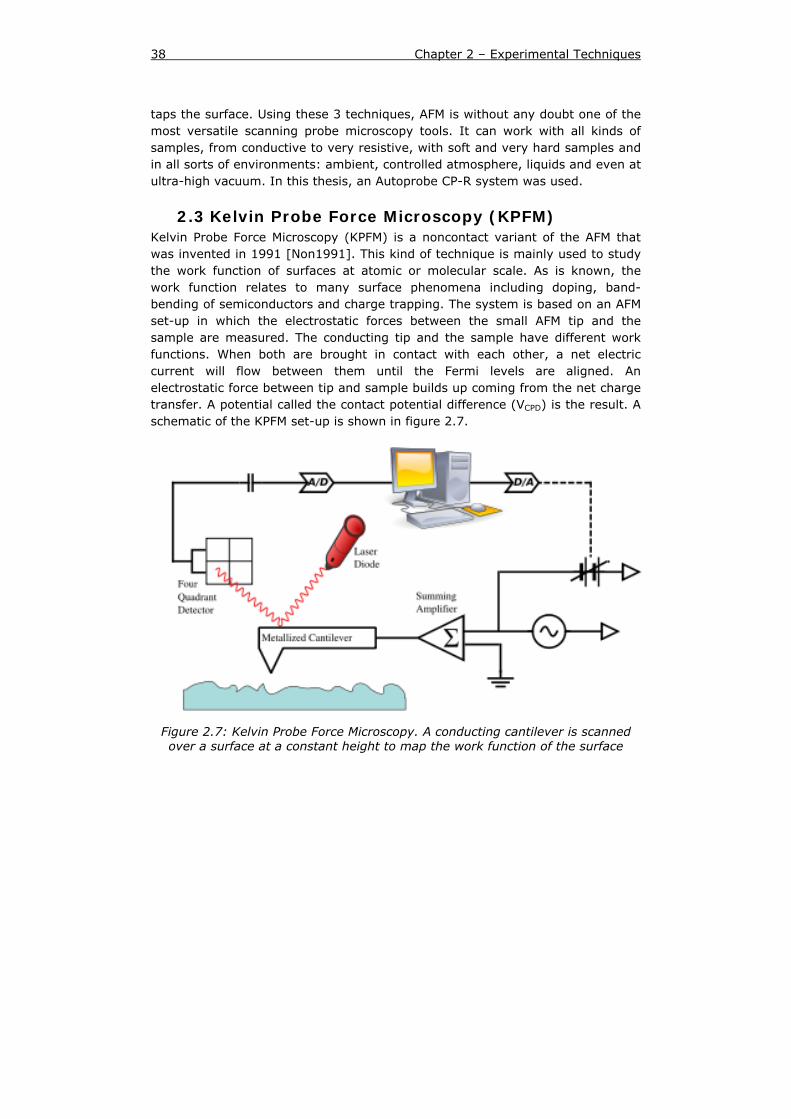
38 Chapter 2 – Experimental Techniques
taps the surface. Using these 3 techniques, AFM is without any doubt one of the most versatile scanning probe microscopy tools. It can work with all kinds of samples, from conductive to very resistive, with soft and very hard samples and in all sorts of environments: ambient, controlled atmosphere, liquids and even at ultra-high vacuum. In this thesis, an Autoprobe CP-R system was used.
2.3 Kelvin Probe Force Microscopy (KPFM) Kelvin Probe Force Microscopy (KPFM) is a noncontact variant of the AFM that was invented in 1991 [Non1991]. This kind of technique is mainly used to study the work function of surfaces at atomic or molecular scale. As is known, the work function relates to many surface phenomena including doping, band-bending of semiconductors and charge trapping. The system is based on an AFM set-up in which the electrostatic forces between the small AFM tip and the sample are measured. The conducting tip and the sample have different work functions. When both are brought in contact with each other, a net electric current will flow between them until the Fermi levels are aligned. An electrostatic force between tip and sample builds up coming from the net charge transfer. A potential called the contact potential difference (VCPD) is the result. A schematic of the KPFM set-up is shown in figure 2.7.
Figure 2.7: Kelvin Probe Force Microscopy. A conducting cantilever is scanned over a surface at a constant height to map the work function of the surface
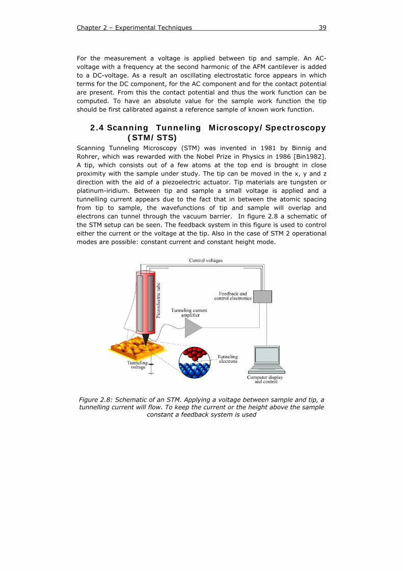
Chapter 2 – Experimental Techniques 39
For the measurement a voltage is applied between tip and sample. An AC-voltage with a frequency at the second harmonic of the AFM cantilever is added to a DC-voltage. As a result an oscillating electrostatic force appears in which terms for the DC component, for the AC component and for the contact potential are present. From this the contact potential and thus the work function can be computed. To have an absolute value for the sample work function the tip should be first calibrated against a reference sample of known work function.
2.4 Scanning Tunneling Microscopy/Spectroscopy (STM/STS)
Scanning Tunneling Microscopy (STM) was invented in 1981 by Binnig and Rohrer, which was rewarded with the Nobel Prize in Physics in 1986 [Bin1982]. A tip, which consists out of a few atoms at the top end is brought in close proximity with the sample under study. The tip can be moved in the x, y and z direction with the aid of a piezoelectric actuator. Tip materials are tungsten or platinum-iridium. Between tip and sample a small voltage is applied and a tunnelling current appears due to the fact that in between the atomic spacing from tip to sample, the wavefunctions of tip and sample will overlap and electrons can tunnel through the vacuum barrier. In figure 2.8 a schematic of the STM setup can be seen. The feedback system in this figure is used to control either the current or the voltage at the tip. Also in the case of STM 2 operational modes are possible: constant current and constant height mode.
Figure 2.8: Schematic of an STM. Applying a voltage between sample and tip, a tunnelling current will flow. To keep the current or the height above the sample
constant a feedback system is used
40 Chapter 2 – Experimental Techniques
When constant current is required, the feedback system regulates the z position of the tip. A constant voltage is applied and while scanning across the surface the z position is recorded to give a topographic map of the surface where a contrast in the image is due to variations in charge density [Bon2001]. In constant height mode, the voltage and height are kept constant. While scanning the surface, the current is recorded giving again information on the charge density.
In addition it is also possible to monitor the current as a function of the applied voltage on one spot I(V). With this technique the local density of states (dI/dV) and the band gap of the surface at the atomic scale can be measured. This technique is called scanning tunnelling spectroscopy (STS). For the STM/STS measurements in this thesis, an Omicron VT (Variable Temperature) AFM/STM is used. As tip, an etched tungsten wire is made use of.
2.5 Secondary Electron Microscopy (SEM) A very small probe of electrons with an energy of 40keV is focused at the surface. Because the wavelength of electrons is smaller than that of photons, this technique can be used to look at structures at the surface which are much smaller than can be seen by normal microscopy. Several processes occur at the surface: backscattering of the incident beam of electrons, secondary electron emission, X-rays and Auger electrons however for SEM the emission of secondary electrons and the backscattering of the primary electrons are the most important processes. The generated secondary electrons have an energy around 10eV. These secondary electrons are detected while scanning the surface. When there is a feature, like a steep incline, on the surface, the angle between the incident beam and the sample surface is different from that of a flat surface, and the intensity of the scattered electrons will change drastically. By correlating the intensity to the position of the scanner an image of the surface can be made. The resolution of the SEM lies around 4nm to 10nm when scanning is performed under vacuum. Therefore, the sample under study must be conductive enough to exclude surface charging and drift of the electron beam. In this study a Philips XL30 FEG with an EDAX DX4i EDS system is used.
2.6 X-ray diffraction To perform the structural characterisation of a crystalline material X-ray diffraction is used, discovered by von Laue in 1912 [Fri1912]. In this non-destructive technique Rontgen radiation is send onto the sample under study. Elastic scattering of X-rays occurs only for structures with long range ordering. The X-rays are scattered in different directions but only constructive interference is happening at angles θ when following the Bragg law
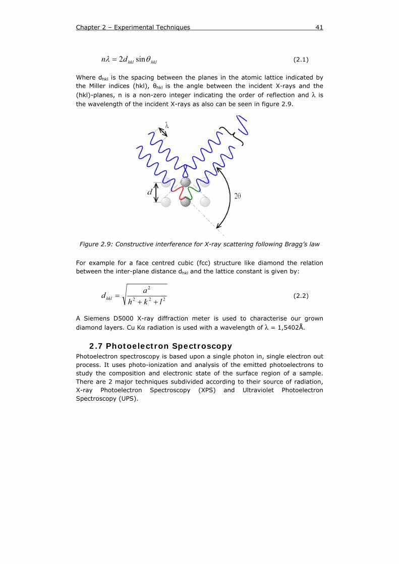
Chapter 2 – Experimental Techniques 41
hklhkldn θλ sin2= (2.1)
Where dhkl is the spacing between the planes in the atomic lattice indicated by the Miller indices (hkl), θhkl is the angle between the incident X-rays and the
(hkl)-planes, n is a non-zero integer indicating the order of reflection and λ is the wavelength of the incident X-rays as also can be seen in figure 2.9.
Figure 2.9: Constructive interference for X-ray scattering following Bragg’s law
For example for a face centred cubic (fcc) structure like diamond the relation between the inter-plane distance dhkl and the lattice constant is given by:
222
2
lkhadhkl ++
= (2.2)
A Siemens D5000 X-ray diffraction meter is used to characterise our grown
diamond layers. Cu Kα radiation is used with a wavelength of λ = 1,5402Å.
2.7 Photoelectron Spectroscopy Photoelectron spectroscopy is based upon a single photon in, single electron out process. It uses photo-ionization and analysis of the emitted photoelectrons to study the composition and electronic state of the surface region of a sample. There are 2 major techniques subdivided according to their source of radiation, X-ray Photoelectron Spectroscopy (XPS) and Ultraviolet Photoelectron Spectroscopy (UPS).

42 Chapter 2 – Experimental Techniques
2.7.1 X-ray Photoelectron Spectroscopy (XPS) With this technique, monochromatic Rontgen radiation is used to excite electrons from the core (inner shells) of the atoms in the layer under study.
Mg Kα (1253.6eV) and Al Kα (1486.6eV) are frequently used for XPS, but by using synchrotron radiation also other energies for the Rontgen beam are possible. When the energy of the photons, send onto the sample, is larger than the work function of the material, electrons from the inner shells of the atom are emitted. By measuring the energy of these electrons one can predict on the elements present in the sample, because each element has its own typical set of core levels. (equation 2.3)
)( Φ+−= Bkin EhE υ (2.3)
Where Ekin is the measured energy of the excited electrons, hυ is the energy of the Rontgen radiation, EB is the energy of the bounded electron according to the
Fermi level and Ф is the work function as also can be deduced from figure 2.10.
Figure 2.10: Energy scheme of the XPS process
Next to elemental information, XPS can also give chemical information due to the measurement of the binding energy. Because the core levels can change a few eV when there is a different binding of the atoms, which can be detected in the XPS spectrum as a peak shift. A downside of XPS is that only atoms starting from Lithium can be measured so hydrogen and helium cannot be addressed with this technique.
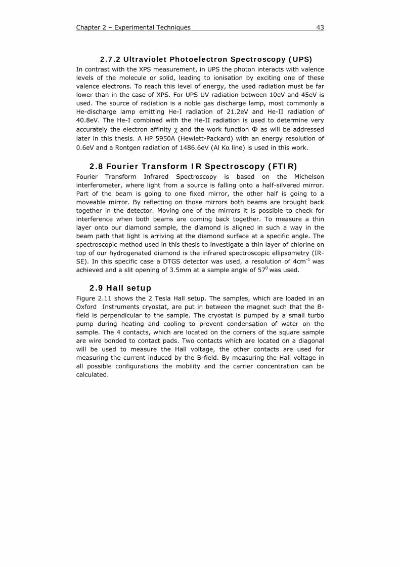
Chapter 2 – Experimental Techniques 43
2.7.2 Ultraviolet Photoelectron Spectroscopy (UPS) In contrast with the XPS measurement, in UPS the photon interacts with valence levels of the molecule or solid, leading to ionisation by exciting one of these valence electrons. To reach this level of energy, the used radiation must be far lower than in the case of XPS. For UPS UV radiation between 10eV and 45eV is used. The source of radiation is a noble gas discharge lamp, most commonly a He-discharge lamp emitting He-I radiation of 21.2eV and He-II radiation of 40.8eV. The He-I combined with the He-II radiation is used to determine very
accurately the electron affinity χ and the work function Ф as will be addressed later in this thesis. A HP 5950A (Hewlett-Packard) with an energy resolution of
0.6eV and a Rontgen radiation of 1486.6eV (Al Kα line) is used in this work.
2.8 Fourier Transform IR Spectroscopy (FTIR) Fourier Transform Infrared Spectroscopy is based on the Michelson interferometer, where light from a source is falling onto a half-silvered mirror. Part of the beam is going to one fixed mirror, the other half is going to a moveable mirror. By reflecting on those mirrors both beams are brought back together in the detector. Moving one of the mirrors it is possible to check for interference when both beams are coming back together. To measure a thin layer onto our diamond sample, the diamond is aligned in such a way in the beam path that light is arriving at the diamond surface at a specific angle. The spectroscopic method used in this thesis to investigate a thin layer of chlorine on top of our hydrogenated diamond is the infrared spectroscopic ellipsometry (IR-SE). In this specific case a DTGS detector was used, a resolution of 4cm-1 was achieved and a slit opening of 3.5mm at a sample angle of 570 was used.
2.9 Hall setup Figure 2.11 shows the 2 Tesla Hall setup. The samples, which are loaded in an Oxford Instruments cryostat, are put in between the magnet such that the B-field is perpendicular to the sample. The cryostat is pumped by a small turbo pump during heating and cooling to prevent condensation of water on the sample. The 4 contacts, which are located on the corners of the square sample are wire bonded to contact pads. Two contacts which are located on a diagonal will be used to measure the Hall voltage, the other contacts are used for measuring the current induced by the B-field. By measuring the Hall voltage in all possible configurations the mobility and the carrier concentration can be calculated.
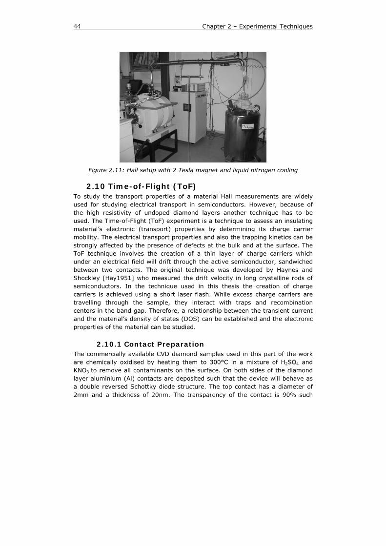
44 Chapter 2 – Experimental Techniques
Figure 2.11: Hall setup with 2 Tesla magnet and liquid nitrogen cooling
2.10 Time-of-Flight (ToF) To study the transport properties of a material Hall measurements are widely used for studying electrical transport in semiconductors. However, because of the high resistivity of undoped diamond layers another technique has to be used. The Time-of-Flight (ToF) experiment is a technique to assess an insulating material’s electronic (transport) properties by determining its charge carrier mobility. The electrical transport properties and also the trapping kinetics can be strongly affected by the presence of defects at the bulk and at the surface. The ToF technique involves the creation of a thin layer of charge carriers which under an electrical field will drift through the active semiconductor, sandwiched between two contacts. The original technique was developed by Haynes and Shockley [Hay1951] who measured the drift velocity in long crystalline rods of semiconductors. In the technique used in this thesis the creation of charge carriers is achieved using a short laser flash. While excess charge carriers are travelling through the sample, they interact with traps and recombination centers in the band gap. Therefore, a relationship between the transient current and the material’s density of states (DOS) can be established and the electronic properties of the material can be studied.
2.10.1 Contact Preparation The commercially available CVD diamond samples used in this part of the work are chemically oxidised by heating them to 300°C in a mixture of H2SO4 and KNO3 to remove all contaminants on the surface. On both sides of the diamond layer aluminium (Al) contacts are deposited such that the device will behave as a double reversed Schottky diode structure. The top contact has a diameter of 2mm and a thickness of 20nm. The transparency of the contact is 90% such
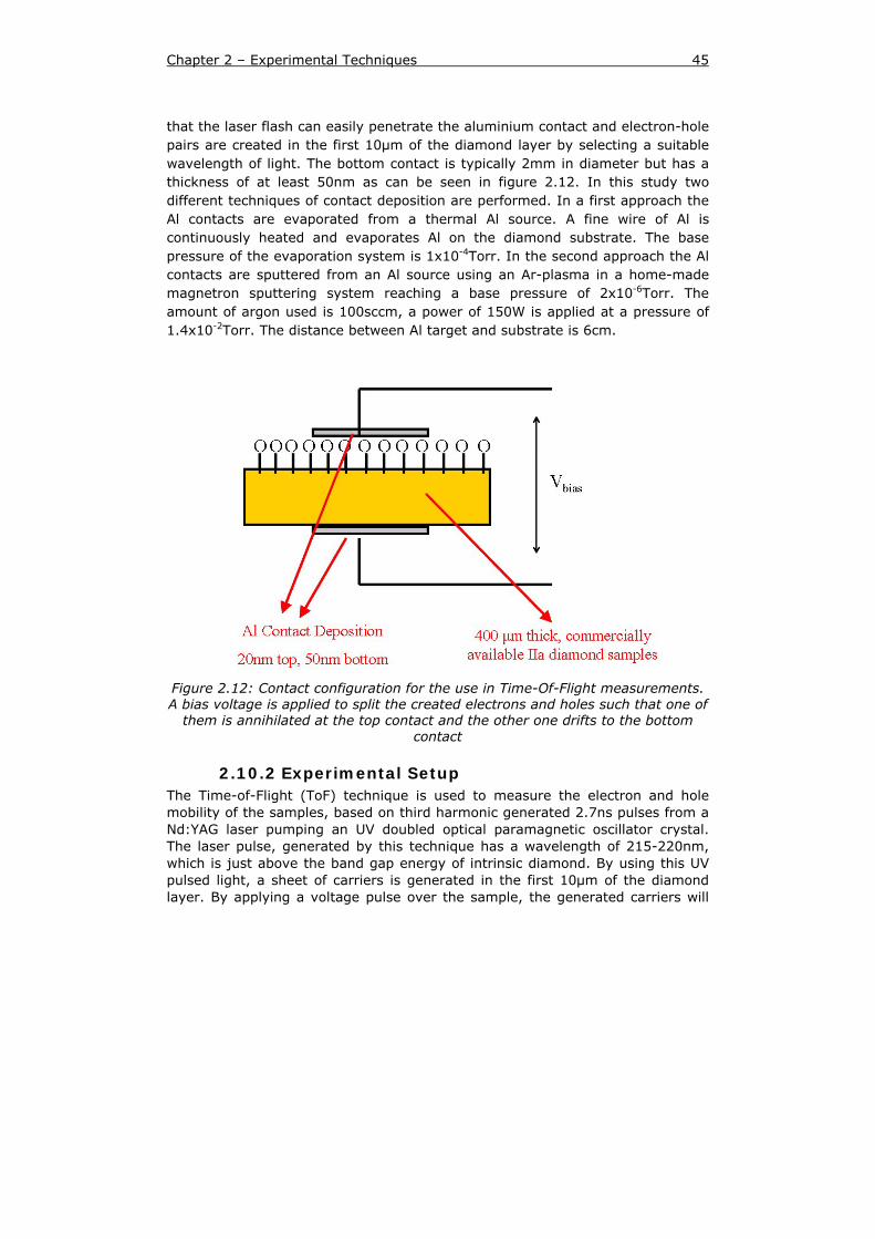
Chapter 2 – Experimental Techniques 45
that the laser flash can easily penetrate the aluminium contact and electron-hole pairs are created in the first 10μm of the diamond layer by selecting a suitable wavelength of light. The bottom contact is typically 2mm in diameter but has a thickness of at least 50nm as can be seen in figure 2.12. In this study two different techniques of contact deposition are performed. In a first approach the Al contacts are evaporated from a thermal Al source. A fine wire of Al is continuously heated and evaporates Al on the diamond substrate. The base pressure of the evaporation system is 1x10⁻⁴Torr. In the second approach the Al contacts are sputtered from an Al source using an Ar-plasma in a home-made magnetron sputtering system reaching a base pressure of 2x10⁻⁶Torr. The amount of argon used is 100sccm, a power of 150W is applied at a pressure of 1.4x10⁻²Torr. The distance between Al target and substrate is 6cm.
Figure 2.12: Contact configuration for the use in Time-Of-Flight measurements. A bias voltage is applied to split the created electrons and holes such that one of
them is annihilated at the top contact and the other one drifts to the bottom contact
2.10.2 Experimental Setup The Time-of-Flight (ToF) technique is used to measure the electron and hole mobility of the samples, based on third harmonic generated 2.7ns pulses from a Nd:YAG laser pumping an UV doubled optical paramagnetic oscillator crystal. The laser pulse, generated by this technique has a wavelength of 215-220nm, which is just above the band gap energy of intrinsic diamond. By using this UV pulsed light, a sheet of carriers is generated in the first 10μm of the diamond layer. By applying a voltage pulse over the sample, the generated carriers will

46 Chapter 2 – Experimental Techniques
be divided depending on the polarity of the applied electric field. If a positive voltage pulse is applied, electrons are collected immediately at the top contact and holes are the carriers of interest travelling through the sample. Under a negative voltage pulse, holes are collected and electrons will drift to the bottom contact. The applied voltage pulse can be adjusted from 0 to 5V and is amplified by a factor of 100. The 4ms pulsed electric field, produced by a function generator is applied to the sample assuring a homogeneous electric field before dielectric relaxation occurs. The laser pulse is delayed by 50μs to reduce any induced electric noise and to ensure a good match between electric field and laser pulse. A Si-detector is used to trigger the oscilloscope as can be seen in figure 2.13. A special filter is used to allow only UV light between 215nm and 225nm to pass such that light with a different wavelength is not interfering at the contacts. The measurements are recorded using a 500MHz digital oscilloscope and an averaging was done over 25 measurements to reduce the noise according to the signal. A 15m long coaxial cable is used to dump and shift the reflections on the voltage input side of the sample. The current is measured using a 50Ω impedance matched line [Bog2007].
Figure 2.13: The Time-Of-Flight setup showing the 3ns laser pulse created from an Nd-YAG laser. The Si-detector used as a trigger for the oscilloscope, the 2
function generators for applying a bias voltage over the sample and triggering of the Q-laser-switch are also shown
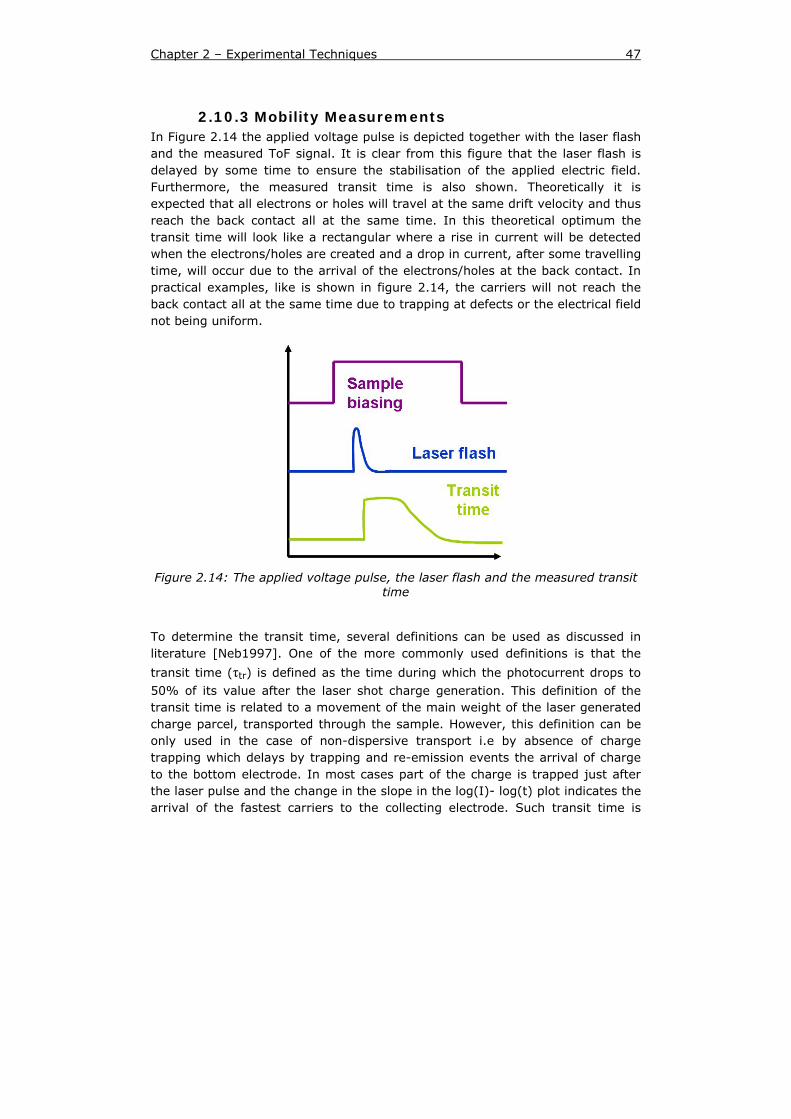
Chapter 2 – Experimental Techniques 47
2.10.3 Mobility Measurements In Figure 2.14 the applied voltage pulse is depicted together with the laser flash and the measured ToF signal. It is clear from this figure that the laser flash is delayed by some time to ensure the stabilisation of the applied electric field. Furthermore, the measured transit time is also shown. Theoretically it is expected that all electrons or holes will travel at the same drift velocity and thus reach the back contact all at the same time. In this theoretical optimum the transit time will look like a rectangular where a rise in current will be detected when the electrons/holes are created and a drop in current, after some travelling time, will occur due to the arrival of the electrons/holes at the back contact. In practical examples, like is shown in figure 2.14, the carriers will not reach the back contact all at the same time due to trapping at defects or the electrical field not being uniform.
Figure 2.14: The applied voltage pulse, the laser flash and the measured transit time
To determine the transit time, several definitions can be used as discussed in literature [Neb1997]. One of the more commonly used definitions is that the
transit time (τtr) is defined as the time during which the photocurrent drops to 50% of its value after the laser shot charge generation. This definition of the transit time is related to a movement of the main weight of the laser generated charge parcel, transported through the sample. However, this definition can be only used in the case of non-dispersive transport i.e by absence of charge trapping which delays by trapping and re-emission events the arrival of charge to the bottom electrode. In most cases part of the charge is trapped just after the laser pulse and the change in the slope in the log(I)- log(t) plot indicates the arrival of the fastest carriers to the collecting electrode. Such transit time is

48 Chapter 2 – Experimental Techniques
directly related to the microscopic drift mobility, defined as a time needed for the fastest carriers to travel through the sample from the front to the back
electrode without any trapping. This definition of τtr is used throughout this thesis. To calculate the electron and hole mobility for low electric fields we should start from the applied electric field. As is generally known, when applying
an electric field Er
, carriers will experience a force Eqr
− and they will
accelerate in that direction until they collide with lattice atoms, impurity atoms
or other scattering centers. The charge carriers have a thermal velocity thvr and
a drift velocity dvr where, for low electric fields the drift velocity is much smaller
than the thermal velocity and proportional to the electric field:
Evd
rr μ= (2.4)
Where the constant μ is called the mobility. When the electric field is increasing,
the drift velocity starts to saturate towards the so called saturation velocity satvr
which for diamond at room temperature is 2x107cm/s for electrons as well as for holes and is correlated to the drift velocity according to equation 2.5.
sat
d
vE
Evr
r
rr
μμ
+=
1 (2.5)
The charge carrier transport can be influenced by impurities or defects. High mobilities and saturation velocities are an important sign for low impurity or defect concentration [Som2002]. When measuring the drift mobility for low electric fields it is important to make a distinction between the two most common modes in Time-of-Flight. When electron-hole pairs of total charge Q are generated by a laser flash within a sample of capacitance C and a voltage of magnitude U two modes are possible: small signal ToF is applicable only if Q<<C.U. For Q>>C.U the space charge limited current (SCLC) mode is reached. In the latter regime, a reservoir of carriers is created near the top contact screening the electric field. The Time-of-Flight signal has a specific shape composed of two maxima, where the first peak results from the time dependent screening field and the second one from the arrival of the first charge carriers at the bottom electrode as can be seen in figure 2.15.
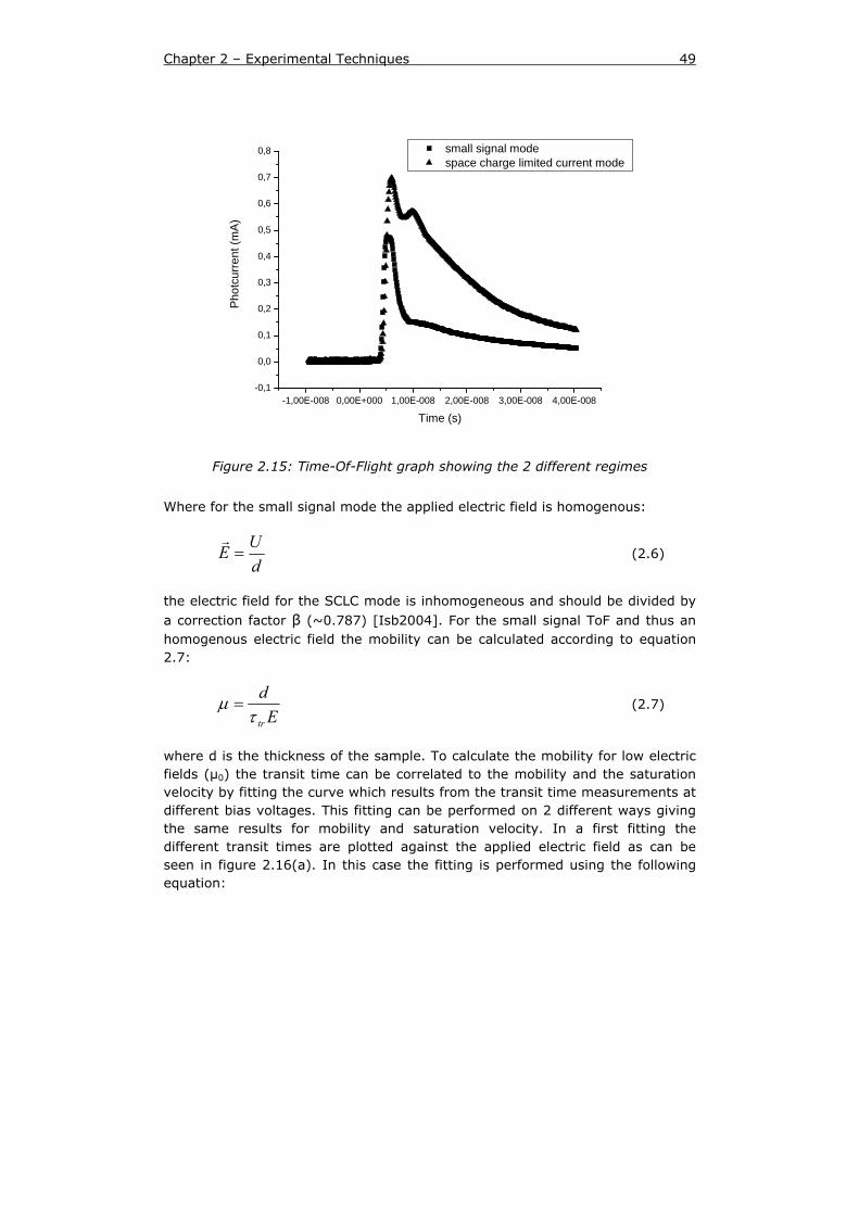
Chapter 2 – Experimental Techniques 49
-1,00E-008 0,00E+000 1,00E-008 2,00E-008 3,00E-008 4,00E-008-0,1
0,0
0,1
0,2
0,3
0,4
0,5
0,6
0,7
0,8
Pho
tcur
rent
(mA
)
Time (s)
small signal mode space charge limited current mode
Figure 2.15: Time-Of-Flight graph showing the 2 different regimes
Where for the small signal mode the applied electric field is homogenous:
dUE =
r (2.6)
the electric field for the SCLC mode is inhomogeneous and should be divided by a correction factor β (~0.787) [Isb2004]. For the small signal ToF and thus an homogenous electric field the mobility can be calculated according to equation 2.7:
Ed
trτμ = (2.7)
where d is the thickness of the sample. To calculate the mobility for low electric fields (μ0) the transit time can be correlated to the mobility and the saturation velocity by fitting the curve which results from the transit time measurements at different bias voltages. This fitting can be performed on 2 different ways giving the same results for mobility and saturation velocity. In a first fitting the different transit times are plotted against the applied electric field as can be seen in figure 2.16(a). In this case the fitting is performed using the following equation:

50 Chapter 2 – Experimental Techniques
satvE0
0
1μμ
μ+
= (2.8)
In a second fitting [Gab2008], the transit times are plotted against the inverse applied voltage such that a linear best fit can be used to determine μ0 and vsat as can be seen in figure 2.16(b) and can be calculated using equation 2.9:
sat
sat
dtr v
dU
dEv
E
dvd
+=+
==0
2
0
01
μμ
μ
τ (2.9)
The slope “a” of the linear fit in figure 2.16(b) can be used to calculate the mobility μ0 where the offset “b” of this fit can be used to calculate the saturation velocity according to equation 2.10:
bdv
ad
sat =
=2
0μ (2.10)
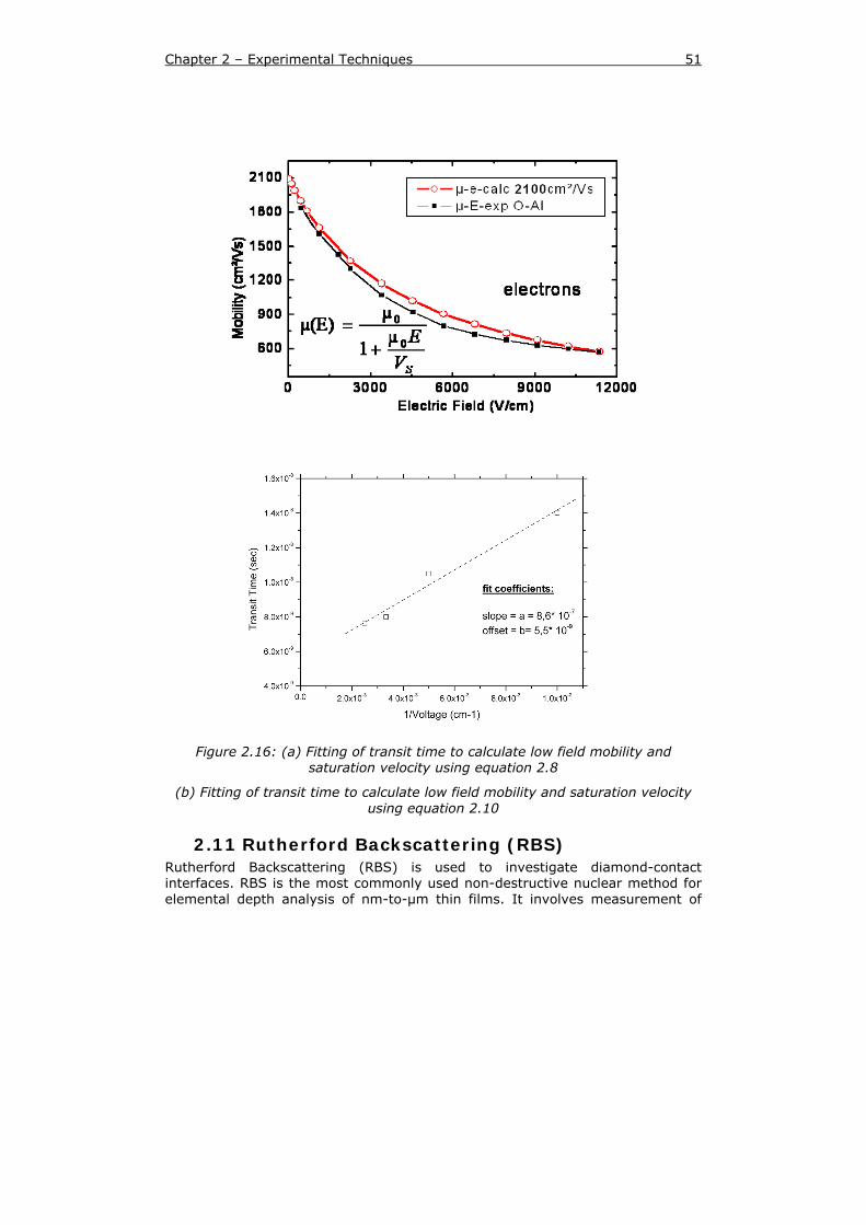
Chapter 2 – Experimental Techniques 51
Figure 2.16: (a) Fitting of transit time to calculate low field mobility and saturation velocity using equation 2.8
(b) Fitting of transit time to calculate low field mobility and saturation velocity using equation 2.10
2.11 Rutherford Backscattering (RBS) Rutherford Backscattering (RBS) is used to investigate diamond-contact interfaces. RBS is the most commonly used non-destructive nuclear method for elemental depth analysis of nm-to-μm thin films. It involves measurement of
52 Chapter 2 – Experimental Techniques
number and energy distribution of energetic ions (usually protons or He+) elastically backscattered within the near-surface region of solid targets. From such measurements it is possible to determine, with some limitations, both the atomic mass and concentration of elemental target constituents as a function of depth below the surface. An ion beam with an energy of the order of several MeV is provided by an accelerator impinging on a sample located in a vacuum chamber (vacuum of the order 10-3–10-5 Pa). Samples are mounted, several per load, on the table of a goniometer which allows three degrees of freedom, two for the sample position and one for the angle, as such to enable sample changing and manipulation without breaking the vacuum. A passivated implanted planar silicon (PIPS) detector or a surface barrier detector is commonly used for ion detection [Tes1995]. RBS analysis was performed using He+ ions of 2MeV with an incoming angle of 0° and 40°. Spectra were evaluated using software SIMNRA 6.02 [May2006].
2.12 Elastic Recoil Detection Analysis (ERDA) Elastic Recoil Detection Analysis (ERDA) is one of the most useful ion-beam analysis techniques for depth profiling of light elements. A beam of energetic ions is directed to the sample. When the incident ion’s mass is larger than the mass of the target atoms in the sample a forward scattering geometry can be used to detect the recoiling light atoms which emerge after collisions with the heavier incident ions. Atoms recoiled from the surface appear at different energies for the different elements as can be seen from figure 2.17 and from reference [Tir1996]. The basic experimental equipment is similar as in RBS, but the glancing geometry with very small incident angles is usually used. ERDA relies on the ability to discriminate between forward-scattered incident ions and recoiling light atoms. The typical experimental arrangement is Mylar foil placed in front of the detector to block out the scattered incident ions but allow the lighter recoiled atoms, which suffer considerably less energy loss, to pass through to the detector. ERDA measurements use ion beam He+ ions of 2 MeV and an incoming angle of 75°. A detector of elastically recoiled hydrogen was covered by Mylar foil with a thickness of 12μm to stop back-scattered He+ ions. Spectra were evaluated using software SIMNRA 6.02 [May2006].
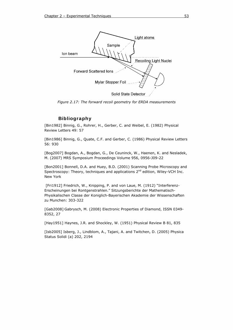
Chapter 2 – Experimental Techniques 53
Figure 2.17: The forward recoil geometry for ERDA measurements
Bibliography [Bin1982] Binnig, G., Rohrer, H., Gerber, C. and Weibel, E. (1982) Physical Review Letters 49: 57
[Bin1986] Binnig, G., Quate, C.F. and Gerber, C. (1986) Physical Review Letters 56: 930
[Bog2007] Bogdan, A., Bogdan, G., De Ceuninck, W., Haenen, K. and Nesladek, M. (2007) MRS Symposium Proceedings Volume 956, 0956-J09-22
[Bon2001] Bonnell, D.A. and Huey, B.D. (2001) Scanning Probe Microscopy and Spectroscopy: Theory, techniques and applications 2nd edition, Wiley-VCH Inc. New York
[Fri1912] Friedrich, W., Knipping, P. and von Laue, M. (1912) “Interferenz-Erscheinungen bei Rontgenstrahlen.” Sitzungsberichte der Mathematisch-Physikalischen Classe der Koniglich-Bayerischen Akademie der Wissenschaften zu Munchen: 303-322
[Gab2008] Gabrysch, M. (2008) Electronic Properties of Diamond, ISSN 0349-8352, 27
[Hay1951] Haynes, J.R. and Shockley, W. (1951) Physical Review B 81, 835
[Isb2005] Isberg, J., Lindblom, A., Tajani, A. and Twitchen, D. (2005) Physica Status Solidi (a) 202, 2194
54 Chapter 2 – Experimental Techniques
[May2006] Mayer, M. (2006) SIMNRA version 6.01 user’s guide, Max-Planck Inst. für Plasmaphysik, Garching
[Neb1997] Nebel, C.E., Munz, J., Stutzmann, M., Zachai, R. and Guttler, H. (1997) Physical Review B 55, 9786
[Non1991] Nonnenmacher, M., O’Boyle, M.P., Wickramasinghe, H.K., Appl. Phys. Lett. 58 (1991) 2921
[Som2002] Somogyi, K. (2002) Diamond and Related Materials 11 (3-6), 686
[Tes1995] Tesmer, J.R. and Nastasi, M. (1995) Handbook of Modern Ion Beam Materials Analysis, Eds: Material Research Society, Pitsburg, Pensylvania
[Tir1996] Tirira, J., Serruys, Y. and Trocellier, P. (1996) Forward Recoil Spectrometry, New York, Plenum Press, USA
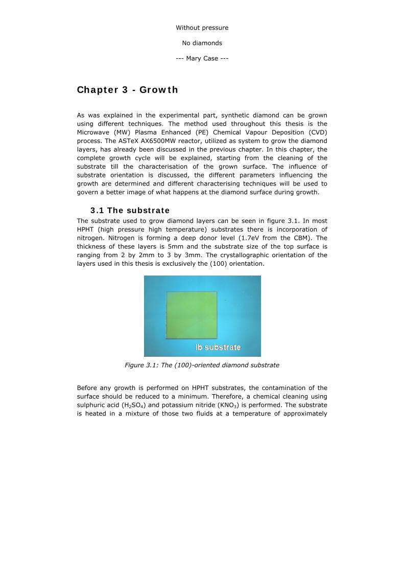
Without pressure
No diamonds
--- Mary Case ---
Chapter 3 - Growth
As was explained in the experimental part, synthetic diamond can be grown using different techniques. The method used throughout this thesis is the Microwave (MW) Plasma Enhanced (PE) Chemical Vapour Deposition (CVD) process. The ASTeX AX6500MW reactor, utilized as system to grow the diamond layers, has already been discussed in the previous chapter. In this chapter, the complete growth cycle will be explained, starting from the cleaning of the substrate till the characterisation of the grown surface. The influence of substrate orientation is discussed, the different parameters influencing the growth are determined and different characterising techniques will be used to govern a better image of what happens at the diamond surface during growth.
3.1 The substrate The substrate used to grow diamond layers can be seen in figure 3.1. In most HPHT (high pressure high temperature) substrates there is incorporation of nitrogen. Nitrogen is forming a deep donor level (1.7eV from the CBM). The thickness of these layers is 5mm and the substrate size of the top surface is ranging from 2 by 2mm to 3 by 3mm. The crystallographic orientation of the layers used in this thesis is exclusively the (100) orientation.
Figure 3.1: The (100)-oriented diamond substrate
Before any growth is performed on HPHT substrates, the contamination of the surface should be reduced to a minimum. Therefore, a chemical cleaning using sulphuric acid (H2SO4) and potassium nitride (KNO3) is performed. The substrate is heated in a mixture of those two fluids at a temperature of approximately

56 Chapter 3 – Growth
300°C for 30 minutes. After this heating, the sample is taken out of the mixture and is cleaned with a DI-water procedure. For 5 minutes it is heated in di-ionised water to a little bit less than 100°C without letting the water boil. After this the sample is further cleaned in a rinsing bath for another 5 minutes. The last 2 steps (boiling and rinsing) are repeated for 3 times before the sample is dried with dry air (nitrogen) and positioned in the growth chamber. After the growth the mass of the sample is measured. From the difference in mass before and after the growth, the volume V of the grown sample can be calculated from equation 3.1, where mbegin is the mass before growth and mend is the mass after growth. ρ is the density of the diamond, which in our case is 3,52 g/cm³.
52.3beginend mmmV
−=
Δ=
ρ (3.1)
From this equation, if it is assumed that the sample has a surface of 3 by 3mm, the growth thickness of the diamond can be calculated using equation 3.2:
209.0 cmVd = (3.2)
From this the growth rate (μm/h) can be calculated if the amount of growth hours is known.
Another important aspect influencing the epitaxy is the exact orientation of the diamond substrate. In this work only (100)-oriented diamond substrates are utilized but when looked in more detail to this crystallographic orientation it is found that there is a misorientation of a few degrees according to the (100) direction. In literature, it is shown already that a misorientation of a few degrees can have a big influence on the incorporation of defects and growth related dislocations [Bau05]. Therefore, X-ray diffraction and electron backscatter diffraction (EBSD) have been performed on the substrates used in the thesis.
The method used to obtain the misorientation of the substrate is the “monochromator and open detector method“ [Few2003]. The sample is placed on the sample mount so that the sample surface is accurately parallel to the mounting plate. The precision of this basically defines the precision achievable. A suitable reflection should be found with the detector in the wide-open position at the Bragg condition ω’ = θ. This incident angle now corresponds to the Bragg angle plus the crystal to surface plane angle. By rotating the Φ-axis, which is the axis parallel to the substrate table, the intensity will start to decrease unless the misorientation is zero. If the rotation is a full 180° then the angle through which ω must be rotated to recover this intensity is twice the angle between the
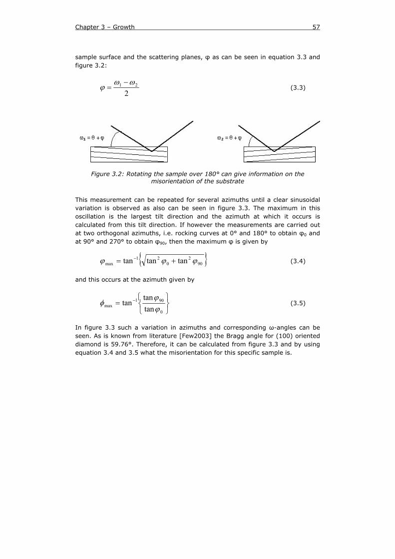
Chapter 3 – Growth 57
sample surface and the scattering planes, φ as can be seen in equation 3.3 and figure 3.2:
221 ωω
ϕ−
= (3.3)
Figure 3.2: Rotating the sample over 180° can give information on the misorientation of the substrate
This measurement can be repeated for several azimuths until a clear sinusoidal variation is observed as also can be seen in figure 3.3. The maximum in this oscillation is the largest tilt direction and the azimuth at which it occurs is calculated from this tilt direction. If however the measurements are carried out at two orthogonal azimuths, i.e. rocking curves at 0° and 180° to obtain φ0 and at 90° and 270° to obtain φ90, then the maximum φ is given by
{ }902
021
max tantantan ϕϕϕ += − (3.4)
and this occurs at the azimuth given by
⎭⎬⎫
⎩⎨⎧
= −
0
901max tan
tantan
ϕϕ
φ (3.5)
In figure 3.3 such a variation in azimuths and corresponding ω-angles can be seen. As is known from literature [Few2003] the Bragg angle for (100) oriented diamond is 59.76°. Therefore, it can be calculated from figure 3.3 and by using equation 3.4 and 3.5 what the misorientation for this specific sample is.

58 Chapter 3 – Growth
°=
°=→°=°=→°=
° 181.0______________________
644.59180005.600
0ϕ
ωφωφ
°=
°=→°=°=→°=
° 804.0______________________
621.60270013.5990
90ϕ
ωφωφ
°=°=
3.7782.0
max
max
φϕ
From this it can be concluded that the maximum misorientation is 0.82° and this misorientation is measured after rotation of the sample over an angle of 77.3°.
Figure 3.3: The rotation of the diamond sample over an angle of 15 degrees gives different omega values. From the sinusoidal variation found by rotating the sample in steps of 15 degrees the misorientation of the diamond surface can be
calculated
Pole figures in the stereographic projection made by Scanning Electron Microscope (SEM) are used to verify the misorientation calculated by XRD measurements. The orientation of an individual crystallite is defined by the position of its unit cell in space with reference to a coordinate system (A, B, C). The unit cell of the face-centered-cubic diamond is represented by a cube. It is
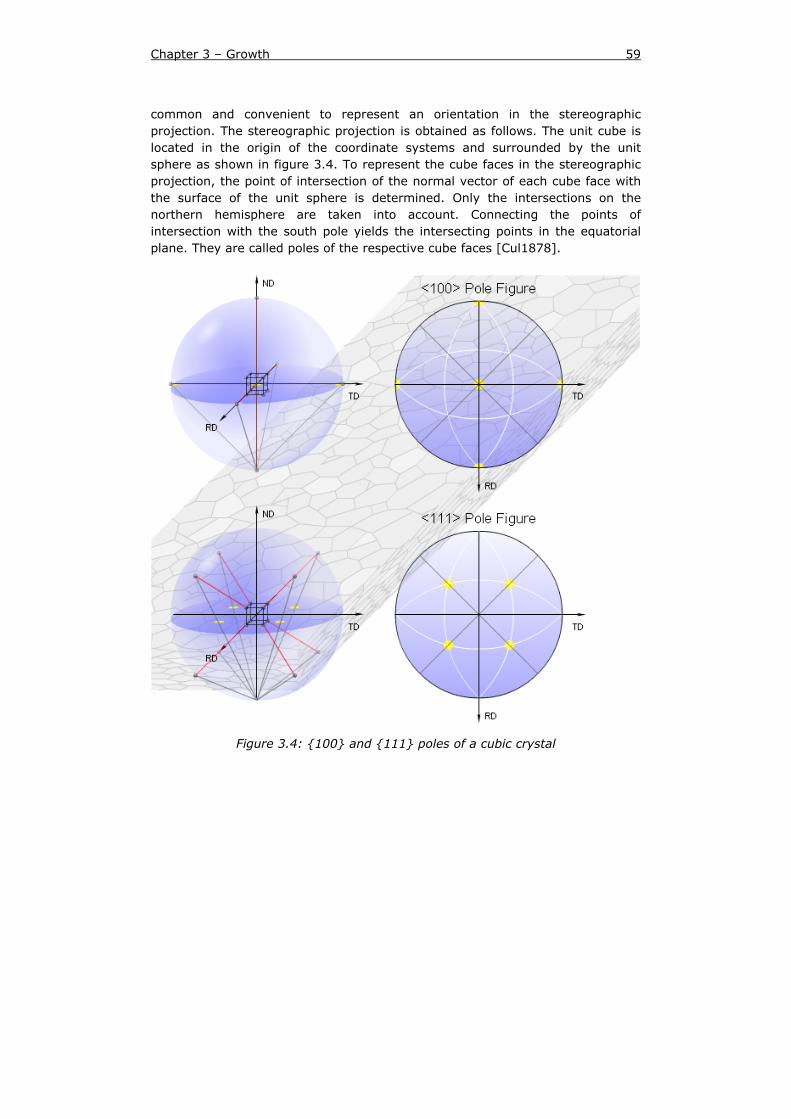
Chapter 3 – Growth 59
common and convenient to represent an orientation in the stereographic projection. The stereographic projection is obtained as follows. The unit cube is located in the origin of the coordinate systems and surrounded by the unit sphere as shown in figure 3.4. To represent the cube faces in the stereographic projection, the point of intersection of the normal vector of each cube face with the surface of the unit sphere is determined. Only the intersections on the northern hemisphere are taken into account. Connecting the points of intersection with the south pole yields the intersecting points in the equatorial plane. They are called poles of the respective cube faces [Cul1878].
Figure 3.4: {100} and {111} poles of a cubic crystal
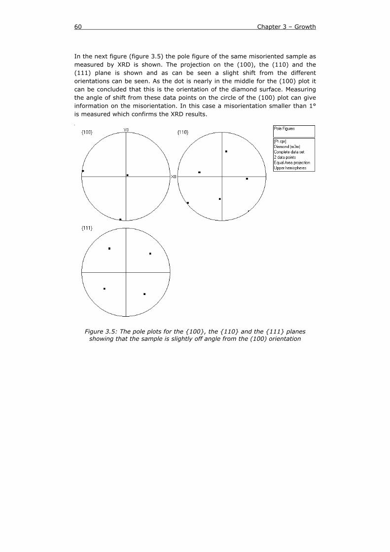
60 Chapter 3 – Growth
In the next figure (figure 3.5) the pole figure of the same misoriented sample as measured by XRD is shown. The projection on the (100), the (110) and the (111) plane is shown and as can be seen a slight shift from the different orientations can be seen. As the dot is nearly in the middle for the (100) plot it can be concluded that this is the orientation of the diamond surface. Measuring the angle of shift from these data points on the circle of the (100) plot can give information on the misorientation. In this case a misorientation smaller than 1° is measured which confirms the XRD results.
Figure 3.5: The pole plots for the {100}, the {110} and the {111} planes showing that the sample is slightly off angle from the (100) orientation
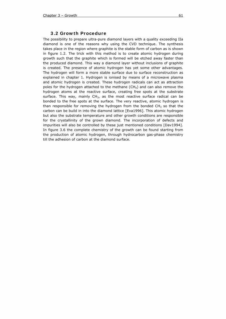
Chapter 3 – Growth 61
3.2 Growth Procedure The possibility to prepare ultra-pure diamond layers with a quality exceeding IIa diamond is one of the reasons why using the CVD technique. The synthesis takes place in the region where graphite is the stable form of carbon as is shown in figure 1.2. The trick with this method is to create atomic hydrogen during growth such that the graphite which is formed will be etched away faster than the produced diamond. This way a diamond layer without inclusions of graphite is created. The presence of atomic hydrogen has yet some other advantages. The hydrogen will form a more stable surface due to surface reconstruction as explained in chapter 1. Hydrogen is ionised by means of a microwave plasma and atomic hydrogen is created. These hydrogen radicals can act as attraction poles for the hydrogen attached to the methane (CH4) and can also remove the hydrogen atoms at the reactive surface, creating free spots at the substrate surface. This way, mainly CH3, as the most reactive surface radical can be bonded to the free spots at the surface. The very reactive, atomic hydrogen is than responsible for removing the hydrogen from the bonded CH3 so that the carbon can be build in into the diamond lattice [Eva1996]. This atomic hydrogen but also the substrate temperature and other growth conditions are responsible for the crystallinity of the grown diamond. The incorporation of defects and impurities will also be controlled by these just mentioned conditions [Dav1994]. In figure 3.6 the complete chemistry of the growth can be found starting from the production of atomic hydrogen, through hydrocarbon gas-phase chemistry till the adhesion of carbon at the diamond surface.
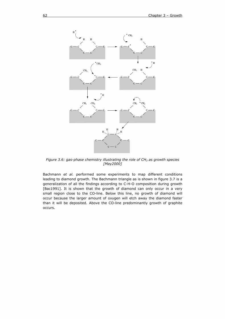
62 Chapter 3 – Growth
Figure 3.6: gas-phase chemistry illustrating the role of CH3 as growth species [May2000]
Bachmann et al. performed some experiments to map different conditions leading to diamond growth. The Bachmann triangle as is shown in figure 3.7 is a generalization of all the findings according to C-H-O composition during growth [Bac1991]. It is shown that the growth of diamond can only occur in a very small region close to the CO-line. Below this line, no growth of diamond will occur because the larger amount of oxygen will etch away the diamond faster than it will be deposited. Above the CO-line predominantly growth of graphite occurs.

Chapter 3 – Growth 63
Figure 3.7: The Bachmann triangle showing the region where diamond can be grown. It should be noticed that a small addition of methane leads to only a very
small region where diamond can be deposited [May2000]
When using the microwave plasma enhanced CVD (MW PE CVD) method to grow diamond layers, the plasma will be generated by microwaves. These microwaves have a frequency of 2.45 GHz or 945 MHz and they are transferred through a rectangular and cylindrical waveguide entering the deposition chamber by a dielectric window. The deposition chamber is designed in such a way that only one resonance frequency is available. A schematic view of the system used to grow our layers is depicted in figure 3.8.
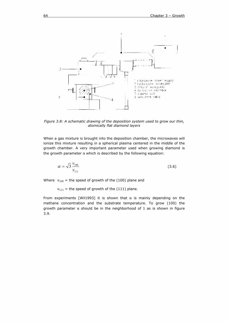
64 Chapter 3 – Growth
Figure 3.8: A schematic drawing of the deposition system used to grow our thin, atomically flat diamond layers
When a gas mixture is brought into the deposition chamber, the microwaves will ionize this mixture resulting in a spherical plasma centered in the middle of the growth chamber. A very important parameter used when growing diamond is
the growth parameter α which is described by the following equation:
111
1003vv
=α (3.6)
Where v100 = the speed of growth of the (100) plane and
v111 = the speed of growth of the (111) plane.
From experiments [Wil1993] it is shown that α is mainly depending on the methane concentration and the substrate temperature. To grow (100) the
growth parameter α should be in the neighborhood of 1 as is shown in figure 3.9.
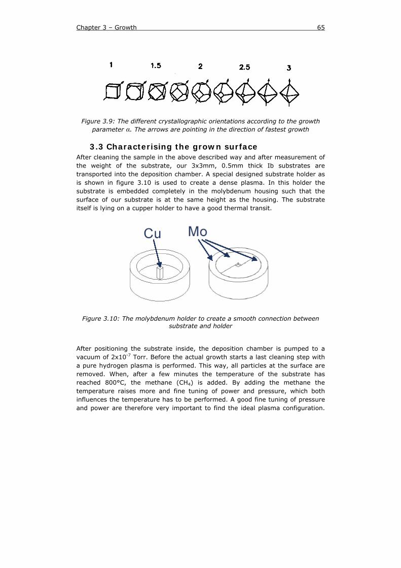
Chapter 3 – Growth 65
Figure 3.9: The different crystallographic orientations according to the growth parameter α. The arrows are pointing in the direction of fastest growth
3.3 Characterising the grown surface After cleaning the sample in the above described way and after measurement of the weight of the substrate, our 3x3mm, 0.5mm thick Ib substrates are transported into the deposition chamber. A special designed substrate holder as is shown in figure 3.10 is used to create a dense plasma. In this holder the substrate is embedded completely in the molybdenum housing such that the surface of our substrate is at the same height as the housing. The substrate itself is lying on a cupper holder to have a good thermal transit.
Figure 3.10: The molybdenum holder to create a smooth connection between substrate and holder
After positioning the substrate inside, the deposition chamber is pumped to a vacuum of 2x10⁻⁷ Torr. Before the actual growth starts a last cleaning step with a pure hydrogen plasma is performed. This way, all particles at the surface are removed. When, after a few minutes the temperature of the substrate has reached 800°C, the methane (CH4) is added. By adding the methane the temperature raises more and fine tuning of power and pressure, which both influences the temperature has to be performed. A good fine tuning of pressure and power are therefore very important to find the ideal plasma configuration.
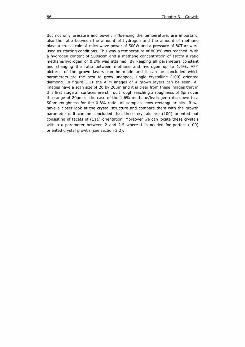
66 Chapter 3 – Growth
But not only pressure and power, influencing the temperature, are important, also the ratio between the amount of hydrogen and the amount of methane plays a crucial role. A microwave power of 500W and a pressure of 80Torr were used as starting conditions. This way a temperature of 800°C was reached. With a hydrogen content of 500sccm and a methane concentration of 1sccm a ratio methane/hydrogen of 0.2% was attained. By keeping all parameters constant and changing the ratio between methane and hydrogen up to 1.6%, AFM pictures of the grown layers can be made and it can be concluded which parameters are the best to grow undoped, single crystalline (100) oriented diamond. In figure 3.11 the AFM images of 4 grown layers can be seen. All images have a scan size of 20 by 20μm and it is clear from these images that in this first stage all surfaces are still quit rough reaching a roughness of 5μm over the range of 20μm in the case of the 1.6% methane/hydrogen ratio down to a 50nm roughness for the 0.8% ratio. All samples show rectangular pits. If we have a closer look at the crystal structure and compare them with the growth
parameter α it can be concluded that these crystals are (100) oriented but consisting of facets of (111) orientation. Moreover we can locate these crystals
with a α-parameter between 2 and 2.5 where 1 is needed for perfect (100) oriented crystal growth (see section 3.2).
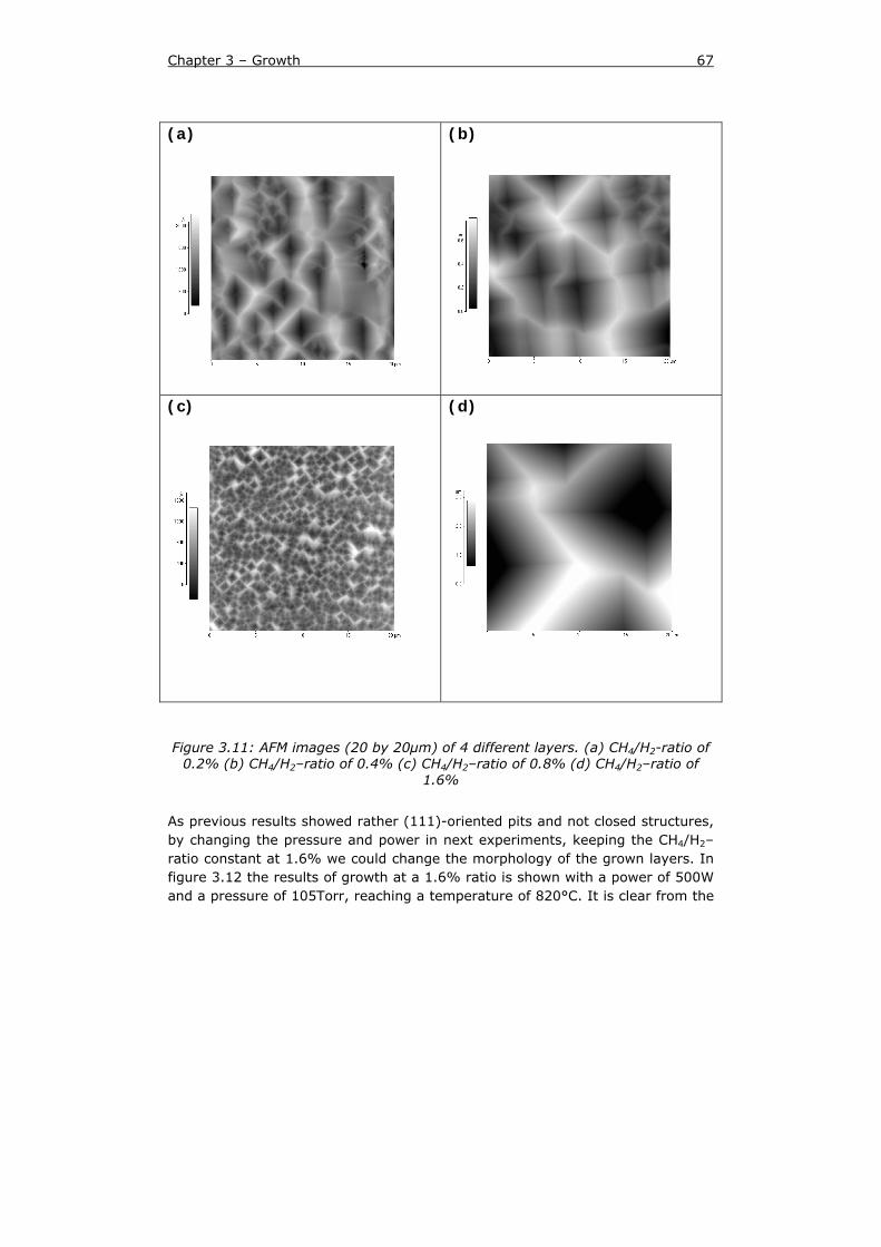
Chapter 3 – Growth 67
Figure 3.11: AFM images (20 by 20μm) of 4 different layers. (a) CH4/H2-ratio of 0.2% (b) CH4/H2–ratio of 0.4% (c) CH4/H2–ratio of 0.8% (d) CH4/H2–ratio of
1.6%
As previous results showed rather (111)-oriented pits and not closed structures, by changing the pressure and power in next experiments, keeping the CH4/H2–ratio constant at 1.6% we could change the morphology of the grown layers. In figure 3.12 the results of growth at a 1.6% ratio is shown with a power of 500W and a pressure of 105Torr, reaching a temperature of 820°C. It is clear from the
(a)
(b)
(c)
(d)
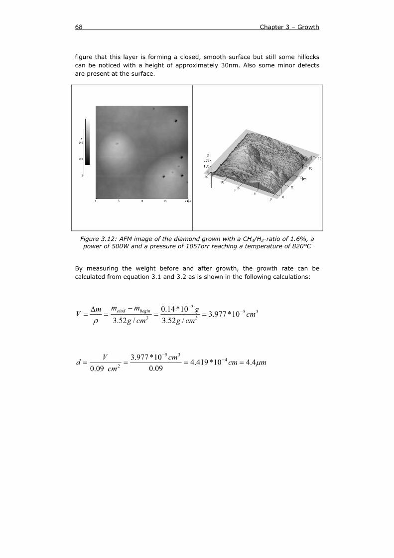
68 Chapter 3 – Growth
figure that this layer is forming a closed, smooth surface but still some hillocks can be noticed with a height of approximately 30nm. Also some minor defects are present at the surface.
Figure 3.12: AFM image of the diamond grown with a CH4/H2-ratio of 1.6%, a power of 500W and a pressure of 105Torr reaching a temperature of 820°C
By measuring the weight before and after growth, the growth rate can be calculated from equation 3.1 and 3.2 as is shown in the following calculations:
353
3
3 10*977.3/52.310*14.0
/52.3cm
cmgg
cmgmmmV begineind −
−
==−
=Δ
=ρ
mcmcmcm
Vd μ4.410*419.409.010*977.3
09.04
35
2 ==== −−
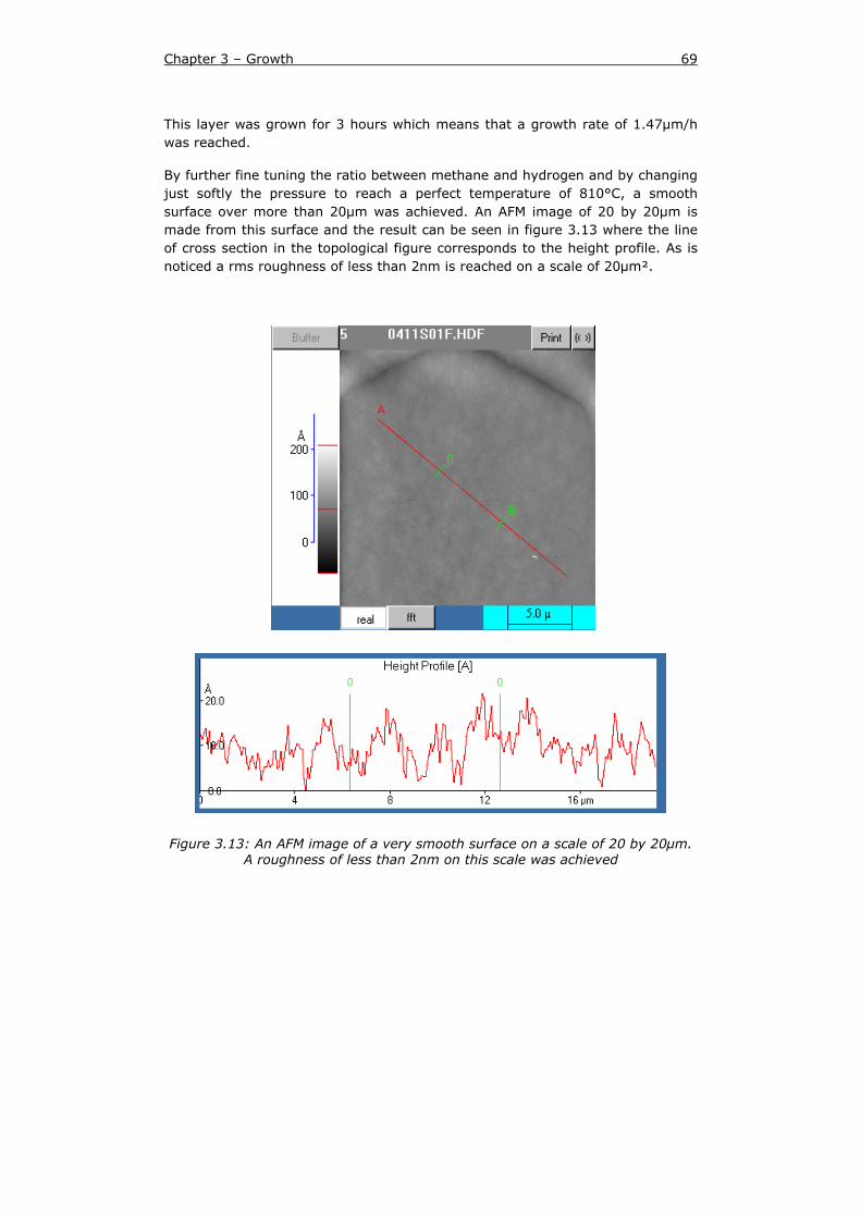
Chapter 3 – Growth 69
This layer was grown for 3 hours which means that a growth rate of 1.47μm/h was reached.
By further fine tuning the ratio between methane and hydrogen and by changing just softly the pressure to reach a perfect temperature of 810°C, a smooth surface over more than 20μm was achieved. An AFM image of 20 by 20μm is made from this surface and the result can be seen in figure 3.13 where the line of cross section in the topological figure corresponds to the height profile. As is noticed a rms roughness of less than 2nm is reached on a scale of 20μm².
Figure 3.13: An AFM image of a very smooth surface on a scale of 20 by 20μm. A roughness of less than 2nm on this scale was achieved
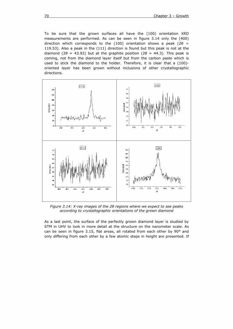
70 Chapter 3 – Growth
To be sure that the grown surfaces all have the (100) orientation XRD measurements are performed. As can be seen in figure 3.14 only the (400) direction which corresponds to the (100) orientation shows a peak (2θ = 119.53). Also a peak in the (111) direction is found but this peak is not at the diamond (2θ = 43.92) but at the graphite position (2θ = 44.3). This peak is coming, not from the diamond layer itself but from the carbon paste which is used to stick the diamond to the holder. Therefore, it is clear that a (100)-oriented layer has been grown without inclusions of other crystallographic directions.
Figure 3.14: X-ray images of the 2θ regions where we expect to see peaks according to crystallographic orientations of the grown diamond
As a last point, the surface of the perfectly grown diamond layer is studied by STM in UHV to look in more detail at the structure on the nanometer scale. As can be seen in figure 3.15, flat areas, all rotated from each other by 90° and only differing from each other by a few atomic steps in height are presented. If
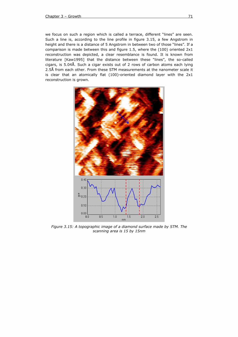
Chapter 3 – Growth 71
we focus on such a region which is called a terrace, different “lines” are seen. Such a line is, according to the line profile in figure 3.15, a few Angstrom in height and there is a distance of 5 Angstrom in between two of those “lines”. If a comparison is made between this and figure 1.5, where the (100) oriented 2x1 reconstruction was depicted, a clear resemblance is found. It is known from literature [Kaw1995] that the distance between these “lines”, the so-called cigars, is 5.04Å. Such a cigar exists out of 2 rows of carbon atoms each lying 2.5Å from each other. From these STM measurements at the nanometer scale it is clear that an atomically flat (100)-oriented diamond layer with the 2x1 reconstruction is grown.
Figure 3.15: A topographic image of a diamond surface made by STM. The scanning area is 15 by 15nm
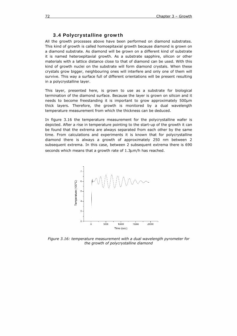
72 Chapter 3 – Growth
3.4 Polycrystalline growth All the growth processes above have been performed on diamond substrates. This kind of growth is called homoepitaxial growth because diamond is grown on a diamond substrate. As diamond will be grown on a different kind of substrate it is named heteroepitaxial growth. As a substrate sapphire, silicon or other materials with a lattice distance close to that of diamond can be used. With this kind of growth nuclei on the substrate will form diamond crystals. When these crystals grow bigger, neighbouring ones will interfere and only one of them will survive. This way a surface full of different orientations will be present resulting in a polycrystalline layer.
This layer, presented here, is grown to use as a substrate for biological termination of the diamond surface. Because the layer is grown on silicon and it needs to become freestanding it is important to grow approximately 500μm thick layers. Therefore, the growth is monitored by a dual wavelength temperature measurement from which the thickness can be deduced.
In figure 3.16 the temperature measurement for the polycrystalline wafer is depicted. After a rise in temperature pointing to the start-up of the growth it can be found that the extrema are always separated from each other by the same time. From calculations and experiments it is known that for polycrystalline diamond there is always a growth of approximately 250 nm between 2 subsequent extrema. In this case, between 2 subsequent extrema there is 690
seconds which means that a growth rate of 1.3μm/h has reached.
Figure 3.16: temperature measurement with a dual wavelength pyrometer for the growth of polycrystalline diamond
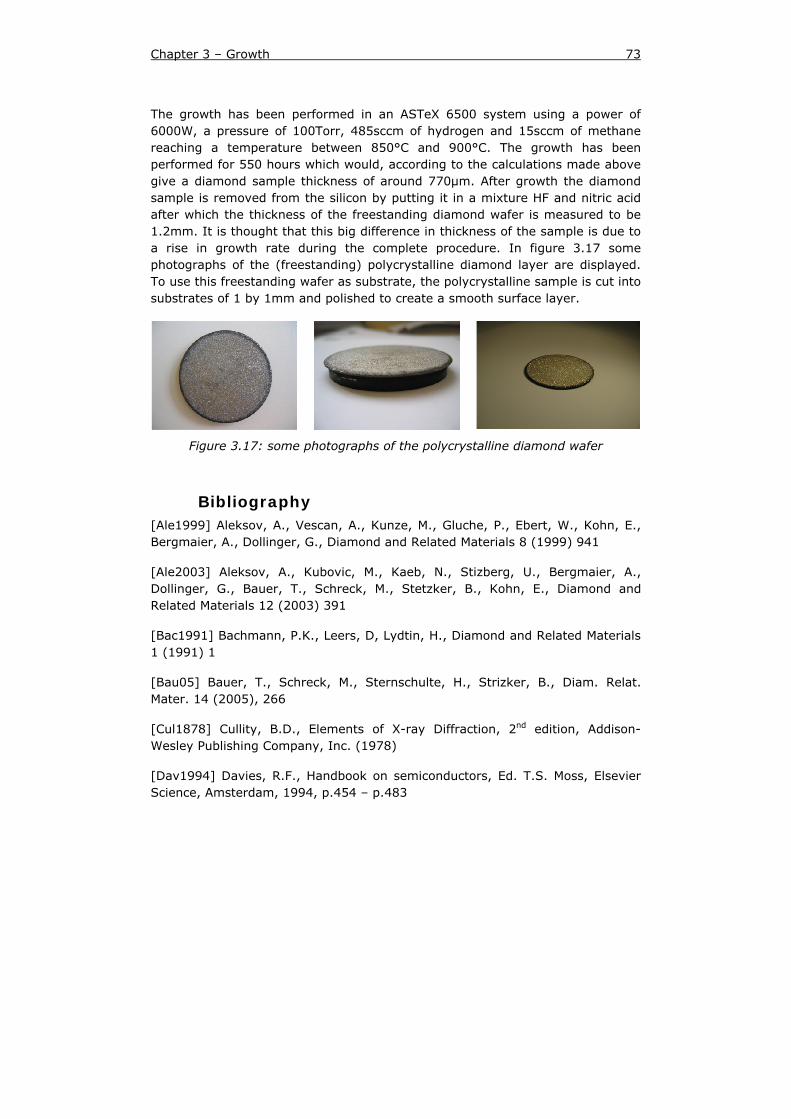
Chapter 3 – Growth 73
The growth has been performed in an ASTeX 6500 system using a power of 6000W, a pressure of 100Torr, 485sccm of hydrogen and 15sccm of methane reaching a temperature between 850°C and 900°C. The growth has been performed for 550 hours which would, according to the calculations made above give a diamond sample thickness of around 770μm. After growth the diamond sample is removed from the silicon by putting it in a mixture HF and nitric acid after which the thickness of the freestanding diamond wafer is measured to be 1.2mm. It is thought that this big difference in thickness of the sample is due to a rise in growth rate during the complete procedure. In figure 3.17 some photographs of the (freestanding) polycrystalline diamond layer are displayed. To use this freestanding wafer as substrate, the polycrystalline sample is cut into substrates of 1 by 1mm and polished to create a smooth surface layer.
Figure 3.17: some photographs of the polycrystalline diamond wafer
Bibliography [Ale1999] Aleksov, A., Vescan, A., Kunze, M., Gluche, P., Ebert, W., Kohn, E., Bergmaier, A., Dollinger, G., Diamond and Related Materials 8 (1999) 941
[Ale2003] Aleksov, A., Kubovic, M., Kaeb, N., Stizberg, U., Bergmaier, A., Dollinger, G., Bauer, T., Schreck, M., Stetzker, B., Kohn, E., Diamond and Related Materials 12 (2003) 391
[Bac1991] Bachmann, P.K., Leers, D, Lydtin, H., Diamond and Related Materials 1 (1991) 1
[Bau05] Bauer, T., Schreck, M., Sternschulte, H., Strizker, B., Diam. Relat. Mater. 14 (2005), 266
[Cul1878] Cullity, B.D., Elements of X-ray Diffraction, 2nd edition, Addison-Wesley Publishing Company, Inc. (1978)
[Dav1994] Davies, R.F., Handbook on semiconductors, Ed. T.S. Moss, Elsevier Science, Amsterdam, 1994, p.454 – p.483
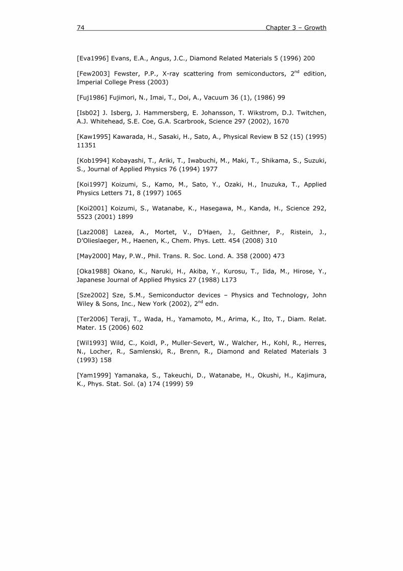
74 Chapter 3 – Growth
[Eva1996] Evans, E.A., Angus, J.C., Diamond Related Materials 5 (1996) 200
[Few2003] Fewster, P.P., X-ray scattering from semiconductors, 2nd edition, Imperial College Press (2003)
[Fuj1986] Fujimori, N., Imai, T., Doi, A., Vacuum 36 (1), (1986) 99
[Isb02] J. Isberg, J. Hammersberg, E. Johansson, T. Wikstrom, D.J. Twitchen, A.J. Whitehead, S.E. Coe, G.A. Scarbrook, Science 297 (2002), 1670
[Kaw1995] Kawarada, H., Sasaki, H., Sato, A., Physical Review B 52 (15) (1995) 11351
[Kob1994] Kobayashi, T., Ariki, T., Iwabuchi, M., Maki, T., Shikama, S., Suzuki, S., Journal of Applied Physics 76 (1994) 1977
[Koi1997] Koizumi, S., Kamo, M., Sato, Y., Ozaki, H., Inuzuka, T., Applied Physics Letters 71, 8 (1997) 1065
[Koi2001] Koizumi, S., Watanabe, K., Hasegawa, M., Kanda, H., Science 292, 5523 (2001) 1899
[Laz2008] Lazea, A., Mortet, V., D’Haen, J., Geithner, P., Ristein, J., D’Olieslaeger, M., Haenen, K., Chem. Phys. Lett. 454 (2008) 310
[May2000] May, P.W., Phil. Trans. R. Soc. Lond. A. 358 (2000) 473
[Oka1988] Okano, K., Naruki, H., Akiba, Y., Kurosu, T., Iida, M., Hirose, Y., Japanese Journal of Applied Physics 27 (1988) L173
[Sze2002] Sze, S.M., Semiconductor devices – Physics and Technology, John Wiley & Sons, Inc., New York (2002), 2nd edn.
[Ter2006] Teraji, T., Wada, H., Yamamoto, M., Arima, K., Ito, T., Diam. Relat. Mater. 15 (2006) 602
[Wil1993] Wild, C., Koidl, P., Muller-Severt, W., Walcher, H., Kohl, R., Herres, N., Locher, R., Samlenski, R., Brenn, R., Diamond and Related Materials 3 (1993) 158
[Yam1999] Yamanaka, S., Takeuchi, D., Watanabe, H., Okushi, H., Kajimura, K., Phys. Stat. Sol. (a) 174 (1999) 59
Diamonds are forever,
Surface conductivity is not
--- Milos Nesladek ---
Chapter 4 - Surface Termination
The aim of this chapter is to study the mechanism of the surface conduction when oxygen is used during the hydrogenation procedure and partially incorporated at the surface. As is discussed in the first chapter (section 1.4.3), by hydrogenating the diamond surface it becomes p-type conductive. Chemisorbed hydrogen is a necessary but not a sufficient prerequisite for such surface conductivity. The electron acceptors which are provided by atmospheric adsorbates and are described in the framework of the so called “transfer surface doping” model [Mai2000] provide a platform for a charge transfer and the generation of a 2DHG layer at the surface. Oxygen can play an important role in this process but its influence is not fully understood [Bob2002]. Therefore, in this chapter, after explaining how the different surface terminations are performed, the influence of oxygen on the hydrogenation process is discussed. STM, STS, XPS and UPS measurements are performed to look at the surface of the diamond layer and the species and bonds that are active on a specific terminated surface. Based on this study a model for the different surface terminations with oxygen is postulated. We discuss how this surface conductivity can be used in experiments creating conductive patterns of resistive areas leading to numerous interesting and promising applications. As a last part of this chapter, the termination of the diamond surface with chlorine and amino is studied with IR-SE and XPS measurements.
4.1 Procedure After growth, the single-crystal diamond layer is chemically oxidised by using the same procedure as described earlier in order to remove all contaminants on the diamond surface. After that, the sample is put back into the deposition chamber which is pumped down to a vacuum of about 6×10⁻⁹Torr and the hydrogenation treatment is carried out in a pure hydrogen plasma or with an oxygen addition (1% or 4% of oxygen in the hydrogen plasma). For this hydrogenation treatment, we create a plasma at a substrate temperature of 700°C and a pressure of 75Torr. A microwave power of 3000W and a hydrogen flow of 1000sccm is used. The plasma is kept on for about 30 seconds after the pressure stabilization (which takes about 2 minutes). After removing the sample from the vessel and a subsequent contact with the ambient, the surface
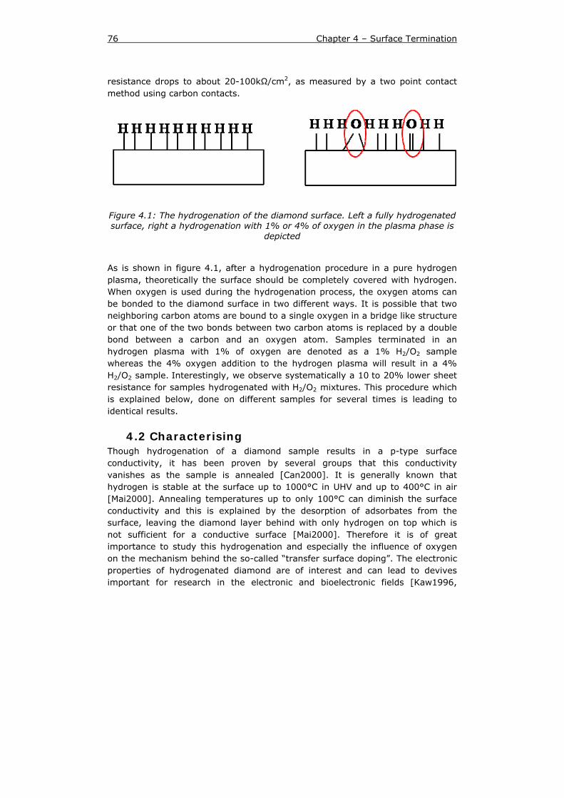
76 Chapter 4 – Surface Termination
resistance drops to about 20-100kΩ/cm2, as measured by a two point contact method using carbon contacts.
Figure 4.1: The hydrogenation of the diamond surface. Left a fully hydrogenated surface, right a hydrogenation with 1% or 4% of oxygen in the plasma phase is
depicted
As is shown in figure 4.1, after a hydrogenation procedure in a pure hydrogen plasma, theoretically the surface should be completely covered with hydrogen. When oxygen is used during the hydrogenation process, the oxygen atoms can be bonded to the diamond surface in two different ways. It is possible that two neighboring carbon atoms are bound to a single oxygen in a bridge like structure or that one of the two bonds between two carbon atoms is replaced by a double bond between a carbon and an oxygen atom. Samples terminated in an hydrogen plasma with 1% of oxygen are denoted as a 1% H2/O2 sample whereas the 4% oxygen addition to the hydrogen plasma will result in a 4% H2/O2 sample. Interestingly, we observe systematically a 10 to 20% lower sheet resistance for samples hydrogenated with H2/O2 mixtures. This procedure which is explained below, done on different samples for several times is leading to identical results.
4.2 Characterising Though hydrogenation of a diamond sample results in a p-type surface conductivity, it has been proven by several groups that this conductivity vanishes as the sample is annealed [Can2000]. It is generally known that hydrogen is stable at the surface up to 1000°C in UHV and up to 400°C in air [Mai2000]. Annealing temperatures up to only 100°C can diminish the surface conductivity and this is explained by the desorption of adsorbates from the surface, leaving the diamond layer behind with only hydrogen on top which is not sufficient for a conductive surface [Mai2000]. Therefore it is of great importance to study this hydrogenation and especially the influence of oxygen on the mechanism behind the so-called “transfer surface doping”. The electronic properties of hydrogenated diamond are of interest and can lead to devives important for research in the electronic and bioelectronic fields [Kaw1996,
Chapter 4 – Surface Termination 77
Gar2003]. To see the influence of oxygen as an adsorbate, diamond samples hydrogenated with a few % of oxygen in the plasma phase are examined by STM measurements. XPS and UPS measurements are used to see the configuration at the surface of the species under study.
4.2.1 STM/STS measurements To examine the influence of oxygen on the surface conductivity, annealing experiments are carried out on the fully hydrogenated and the 1% H2/O2 sample. The 1% H2/O2 sample is placed into the STM in UHV conditions and images are taken before and after two subsequent annealing steps. As can be seen from figure 4.2a, it is very difficult to resolve the surface structure with atomic resolution (scales less than 50 nm). This is probably due to the water adsorbate layer on top of the sample after the hydrogenation process and contact with an ambient environment.
Figure 4.2: STM images of the 1% H2/O2 diamond surface (a) without annealing,
(b) after UHV annealing for 30min at 200°C and (c) after UHV annealing for 30min at 410°C
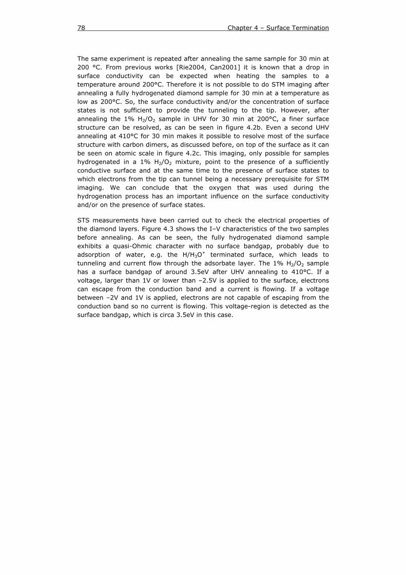
78 Chapter 4 – Surface Termination
The same experiment is repeated after annealing the same sample for 30 min at 200 °C. From previous works [Rie2004, Can2001] it is known that a drop in surface conductivity can be expected when heating the samples to a temperature around 200°C. Therefore it is not possible to do STM imaging after annealing a fully hydrogenated diamond sample for 30 min at a temperature as low as 200°C. So, the surface conductivity and/or the concentration of surface states is not sufficient to provide the tunneling to the tip. However, after annealing the 1% H2/O2 sample in UHV for 30 min at 200°C, a finer surface structure can be resolved, as can be seen in figure 4.2b. Even a second UHV annealing at 410°C for 30 min makes it possible to resolve most of the surface structure with carbon dimers, as discussed before, on top of the surface as it can be seen on atomic scale in figure 4.2c. This imaging, only possible for samples hydrogenated in a 1% H2/O2 mixture, point to the presence of a sufficiently conductive surface and at the same time to the presence of surface states to which electrons from the tip can tunnel being a necessary prerequisite for STM imaging. We can conclude that the oxygen that was used during the hydrogenation process has an important influence on the surface conductivity and/or on the presence of surface states.
STS measurements have been carried out to check the electrical properties of the diamond layers. Figure 4.3 shows the I–V characteristics of the two samples before annealing. As can be seen, the fully hydrogenated diamond sample exhibits a quasi-Ohmic character with no surface bandgap, probably due to adsorption of water, e.g. the H/H3O
+ terminated surface, which leads to tunneling and current flow through the adsorbate layer. The 1% H2/O2 sample has a surface bandgap of around 3.5eV after UHV annealing to 410°C. If a voltage, larger than 1V or lower than –2.5V is applied to the surface, electrons can escape from the conduction band and a current is flowing. If a voltage between –2V and 1V is applied, electrons are not capable of escaping from the conduction band so no current is flowing. This voltage-region is detected as the surface bandgap, which is circa 3.5eV in this case.
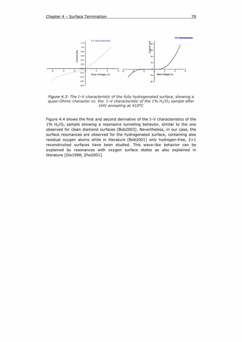
Chapter 4 – Surface Termination 79
Figure 4.3: The I–V characteristic of the fully hydrogenated surface, showing a quasi-Ohmic character vs. the I–V characteristic of the 1% H2/O2 sample after
UHV annealing at 410°C
Figure 4.4 shows the first and second derivative of the I–V characteristics of the 1% H2/O2 sample showing a resonance tunneling behavior, similar to the one observed for clean diamond surfaces [Bob2003]. Nevertheless, in our case, the surface resonances are observed for the hydrogenated surface, containing also residual oxygen atoms while in literature [Bob2001] only hydrogen-free, 2×1 reconstructed surfaces have been studied. This wave-like behavior can be explained by resonances with oxygen surface states as also explained in literature [Die1998, Zhe2001].
80 Chapter 4 – Surface Termination
Figure 4.4: The derivative and second derivative of figure 4.3(b) showing a wave-like behavior pointing to resonances with surface states
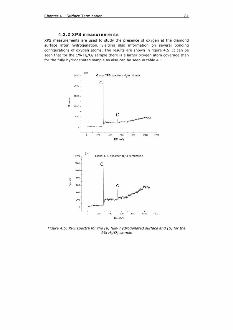
Chapter 4 – Surface Termination 81
4.2.2 XPS measurements XPS measurements are used to study the presence of oxygen at the diamond surface after hydrogenation, yielding also information on several bonding configurations of oxygen atoms. The results are shown in figure 4.5. It can be seen that for the 1% H2/O2 sample there is a larger oxygen atom coverage than for the fully hydrogenated sample as also can be seen in table 4.1.
Figure 4.5: XPS spectra for the (a) fully hydrogenated surface and (b) for the 1% H2/O2 sample
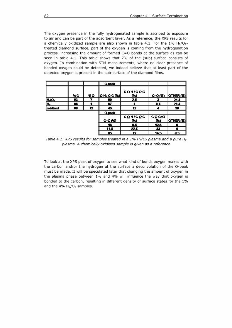
82 Chapter 4 – Surface Termination
The oxygen presence in the fully hydrogenated sample is ascribed to exposure to air and can be part of the adsorbent layer. As a reference, the XPS results for a chemically oxidized sample are also shown in table 4.1. For the 1% H2/O2-treated diamond surface, part of the oxygen is coming from the hydrogenation process, increasing the amount of formed C=O bonds at the surface as can be seen in table 4.1. This table shows that 7% of the (sub)-surface consists of oxygen. In combination with STM measurements, where no clear presence of bonded oxygen could be detected, we indeed believe that at least part of the detected oxygen is present in the sub-surface of the diamond films.
Table 4.1: XPS results for samples treated in a 1% H2/O2 plasma and a pure H2
plasma. A chemically oxidised sample is given as a reference
To look at the XPS peak of oxygen to see what kind of bonds oxygen makes with the carbon and/or the hydrogen at the surface a deconvolution of the O-peak must be made. It will be speculated later that changing the amount of oxygen in the plasma phase between 1% and 4% will influence the way that oxygen is bonded to the carbon, resulting in different density of surface states for the 1% and the 4% H2/O2 samples.
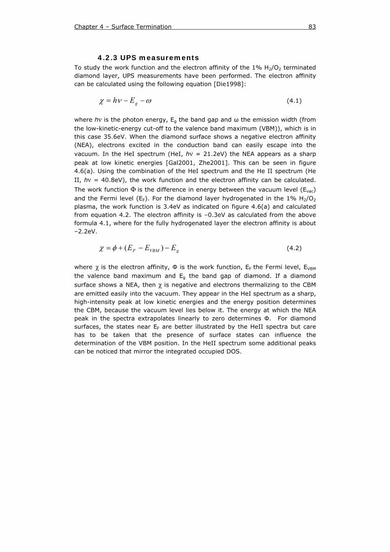
Chapter 4 – Surface Termination 83
4.2.3 UPS measurements To study the work function and the electron affinity of the 1% H2/O2 terminated diamond layer, UPS measurements have been performed. The electron affinity can be calculated using the following equation [Die1998]:
ωνχ −−= gEh (4.1)
where hν is the photon energy, Eg the band gap and ω the emission width (from the low-kinetic-energy cut-off to the valence band maximum (VBM)), which is in this case 35.6eV. When the diamond surface shows a negative electron affinity (NEA), electrons excited in the conduction band can easily escape into the
vacuum. In the HeI spectrum (HeI, hν = 21.2eV) the NEA appears as a sharp peak at low kinetic energies [Gal2001, Zhe2001]. This can be seen in figure 4.6(a). Using the combination of the HeI spectrum and the He II spectrum (He
II, hν = 40.8eV), the work function and the electron affinity can be calculated.
The work function Φ is the difference in energy between the vacuum level (Evac) and the Fermi level (EF). For the diamond layer hydrogenated in the 1% H2/O2 plasma, the work function is 3.4eV as indicated on figure 4.6(a) and calculated from equation 4.2. The electron affinity is –0.3eV as calculated from the above formula 4.1, where for the fully hydrogenated layer the electron affinity is about –2.2eV.
gVBMF EEE −−+= )(φχ (4.2)
where χ is the electron affinity, Φ is the work function, EF the Fermi level, EVBM the valence band maximum and Eg the band gap of diamond. If a diamond
surface shows a NEA, then χ is negative and electrons thermalizing to the CBM are emitted easily into the vacuum. They appear in the HeI spectrum as a sharp, high-intensity peak at low kinetic energies and the energy position determines the CBM, because the vacuum level lies below it. The energy at which the NEA peak in the spectra extrapolates linearly to zero determines Φ. For diamond surfaces, the states near EF are better illustrated by the HeII spectra but care has to be taken that the presence of surface states can influence the determination of the VBM position. In the HeII spectrum some additional peaks can be noticed that mirror the integrated occupied DOS.
84 Chapter 4 – Surface Termination
Figure 4.6: The UPS spectra for the sample hydrogenated in a 1% H2/O2 plasma. The He I spectrum showing a peak corresponding to the NEA of the surface and the He II spectrum showing the fermi level and the work function of this layer
4.2.4 KPFM measurements To check the shift of the Fermi level when the diamond surfaces are differently terminated, KPFM measurements are the preferred tool [Bob2003]. To create a surface where part of the sample is hydrogenated and the other part is oxidised, a checkerboard pattern was created. First the samples were hydrogenated with or without some addition of oxygen during the hydrogenation process. After this hydrogenation process, focused ion beam (FIB) was used to bombard some
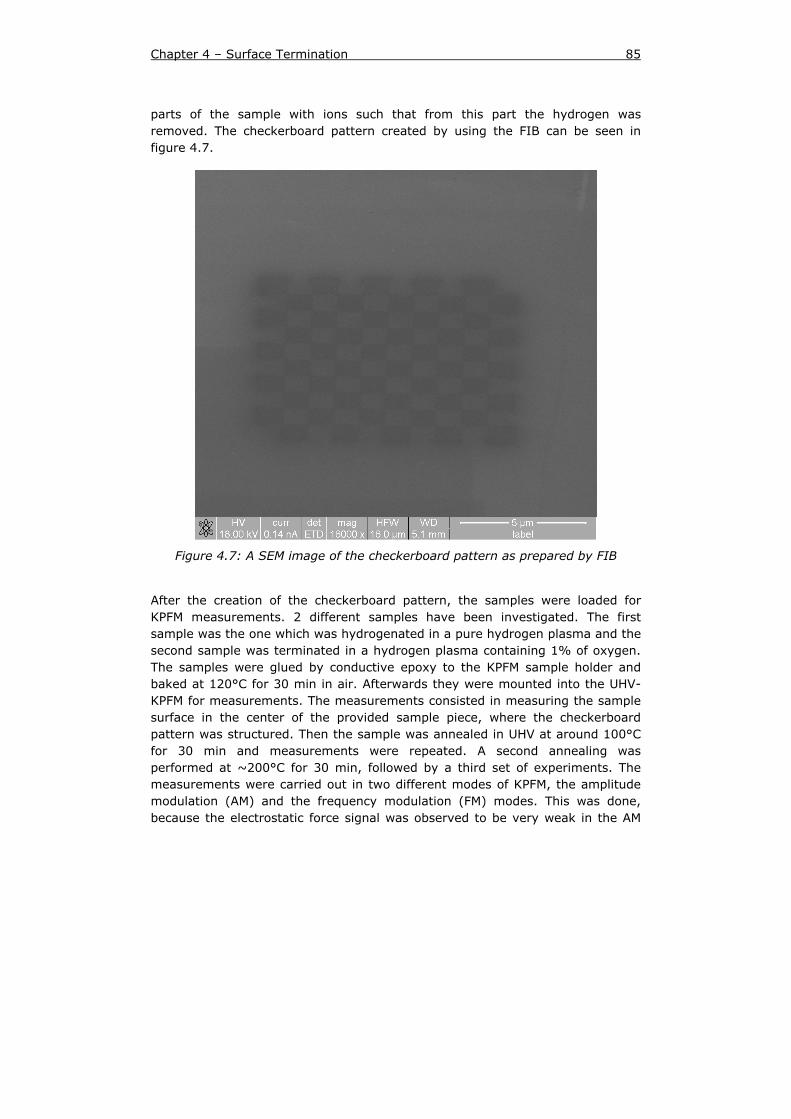
Chapter 4 – Surface Termination 85
parts of the sample with ions such that from this part the hydrogen was removed. The checkerboard pattern created by using the FIB can be seen in figure 4.7.
Figure 4.7: A SEM image of the checkerboard pattern as prepared by FIB
After the creation of the checkerboard pattern, the samples were loaded for KPFM measurements. 2 different samples have been investigated. The first sample was the one which was hydrogenated in a pure hydrogen plasma and the second sample was terminated in a hydrogen plasma containing 1% of oxygen. The samples were glued by conductive epoxy to the KPFM sample holder and baked at 120°C for 30 min in air. Afterwards they were mounted into the UHV-KPFM for measurements. The measurements consisted in measuring the sample surface in the center of the provided sample piece, where the checkerboard pattern was structured. Then the sample was annealed in UHV at around 100°C for 30 min and measurements were repeated. A second annealing was performed at ~200°C for 30 min, followed by a third set of experiments. The measurements were carried out in two different modes of KPFM, the amplitude modulation (AM) and the frequency modulation (FM) modes. This was done, because the electrostatic force signal was observed to be very weak in the AM
86 Chapter 4 – Surface Termination
mode. In AM mode an AC frequency of ~ 450kHz (tuned to the second resonance of the cantilever) and VAC=0.4V was applied to the sample. One suspicion was that the high frequency might cause problems with the surface conductivity of the sample and therefore the electrostatic signal might be so weak. Therefore the FM mode was used, where 1.5V at 1.5kHz was applied to the sample. However, in both modes comparable results were obtained. Summarizing the results, none of the patterned structures as expected before was found. Reasons for this absence could be manifold. Initially the surface is contaminated with adsorbates, water and other molecules, which results in the decoration of the possible work function contrast. Since the sample was introduced from air, this is very likely the reason for the absence of the pattern in the initial measurement. After annealing at ~100°C, this surface contamination should to some extend be gone, however, no work function contrast could be observed. Either there are still some molecules (i.e. carbonhydroxides) which could not be removed at this low temperature, or the pattern was already “damaged” due to the heat treatment (in the 0% sample). The same arguing applies for the higher annealing. However, in the 1% sample, the pattern should be stable against UHV annealing, as stated above. Between the two samples one clear difference was observed. Upon annealing the work function of sample 1 (0%) was not changed by much, where as the work function of sample 2 (1%) was lowered significantly (by 2eV) upon annealing at 120 °C.
4.3 Model From the STS measurements performed in UHV on the 1% H2/O2 sample after annealing at 410°C, some defect levels can be detected in the surface bandgap as can be noticed in figure 4.4. This implies that tunneling can occur to such states if, at the same time, there is a sufficient electrical conductivity to collect the carriers tunneled from the STM tip into the surface states. For the sample hydrogenated only in a pure hydrogen plasma, there is not sufficient conductivity and/or concentration of surface states to carry out STM experiments. Because STM imaging was possible for B-doped H-terminated diamond surfaces [Bob2003, Bob2001] (e.g. there is a sufficient density of hydrogen related surface states as reported in several publications [Bob2003]), we can conclude that it is probably mainly the surface conductivity that limits the STM imaging on undoped samples hydrogenated in a pure H-plasma and subsequently UHV annealed. The hypothesis has been put that for the 1% H2/O2 mixture hydrogenated sample, as soon as the adsorbate related surface conductivity vanishes after the annealing at temperatures of 410°C, another mechanism takes over, leading to a remaining sufficiently high electrical conductivity. To study this hypothesis UPS measurements have been carried out to study the surface states. From the spectrum in figure 4.6, the work function
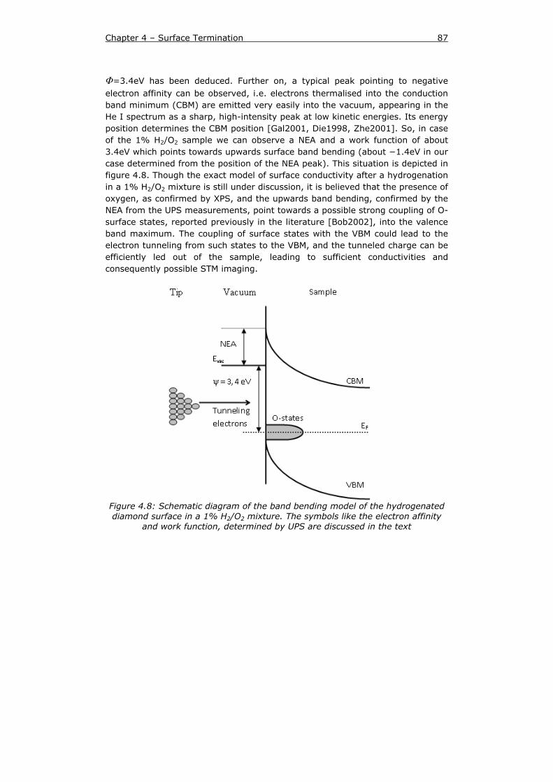
Chapter 4 – Surface Termination 87
Φ=3.4eV has been deduced. Further on, a typical peak pointing to negative electron affinity can be observed, i.e. electrons thermalised into the conduction band minimum (CBM) are emitted very easily into the vacuum, appearing in the He I spectrum as a sharp, high-intensity peak at low kinetic energies. Its energy position determines the CBM position [Gal2001, Die1998, Zhe2001]. So, in case of the 1% H2/O2 sample we can observe a NEA and a work function of about 3.4eV which points towards upwards surface band bending (about −1.4eV in our case determined from the position of the NEA peak). This situation is depicted in figure 4.8. Though the exact model of surface conductivity after a hydrogenation in a 1% H2/O2 mixture is still under discussion, it is believed that the presence of oxygen, as confirmed by XPS, and the upwards band bending, confirmed by the NEA from the UPS measurements, point towards a possible strong coupling of O-surface states, reported previously in the literature [Bob2002], into the valence band maximum. The coupling of surface states with the VBM could lead to the electron tunneling from such states to the VBM, and the tunneled charge can be efficiently led out of the sample, leading to sufficient conductivities and consequently possible STM imaging.
Figure 4.8: Schematic diagram of the band bending model of the hydrogenated diamond surface in a 1% H2/O2 mixture. The symbols like the electron affinity
and work function, determined by UPS are discussed in the text

88 Chapter 4 – Surface Termination
In addition, a different gas mixture is applied to terminate the surface. In this case 4% of oxygen is inserted in the hydrogen plasma. When the 1% H2/O2 sample is compared with the 4% H2/O2 sample some interesting behavior can be seen. First of all, when STM in UHV is performed on the 4% H2/O2 sample no tunneling is possible anymore after a mild annealing to 100°C. This experiment is proving that because of the annealing at 100°C the water layer on top of the diamond surface has been removed and that the surface conductivity associated with the surface hydrogen has vanished. In the 1% H2/O2 case, after this mild annealing still some tunneling with STM in UHV was possible because of the created oxygen defects as explained above. For the 4% H2/O2 sample, because no tunneling is possible anymore, it can be deduced that these oxygen defects, created at the sub-surface are behaving differently from the 1% case. Zheng et al. did some research on the oxygen induced surface states on (100) diamond [Zhe2001] and found that according to the binding of oxygen at the diamond surface a different density of state could be detected as is shown in figure 4.9.
Figure 4.9: (a) DOS of the bridging model of the oxidised diamond surface
(b) DOS of the on-top model of the oxidised diamond surface
Chapter 4 – Surface Termination 89
In this figure computations have been done on the oxidised surface. Two models of oxidised diamond (100) surfaces were used, the bridging (C-O-C) and the on-top (C=O) structure. The calculated s and p partial DOS of diamond as well as the total DOS is shown. Each spectrum in this figure corresponds to an atomic layer starting from the O layer on the top. The DOS of both models shows significant oxygen-induced surface states between -2.2 to -3.4eV. When the different configurations of the carbon-oxygen bond at the surface are compared, it is clear that for the double bounded oxygen, i.e. the on-top model (figure 4.9b) no surface bandgap is created and therefore tunneling in this case is still possible. For the bridging model (figure 4.9a), there is a bandgap of a few eV such that no tunneling is possible for this configuration. This change in DOS can be the possible explanation for the different behavior between the 1% H2/O2 sample and the 4% H2/O2 sample.
4.4 Writing on diamond When a metal is exposed to an oxygen rich atmosphere, this will result in the formation of a natural oxide layer. This oxide layer forms a protecting cover separating the metal from the oxygen rich atmosphere preventing further oxidation. As is explained already before, hydrogenated diamond exhibits a p-type conducting surface. It should therefore be possible to put an oxide layer on the surface by extracting 2 hydrogen atoms from their bonded carbon and replace them by an oxygen atom. An AFM is used to exchange the surface hydrogen with oxygen by letting a current flow through the AFM-tip. In figure 4.10(a) a schematic drawing of such an oxidation process with the aid of an AFM is shown.
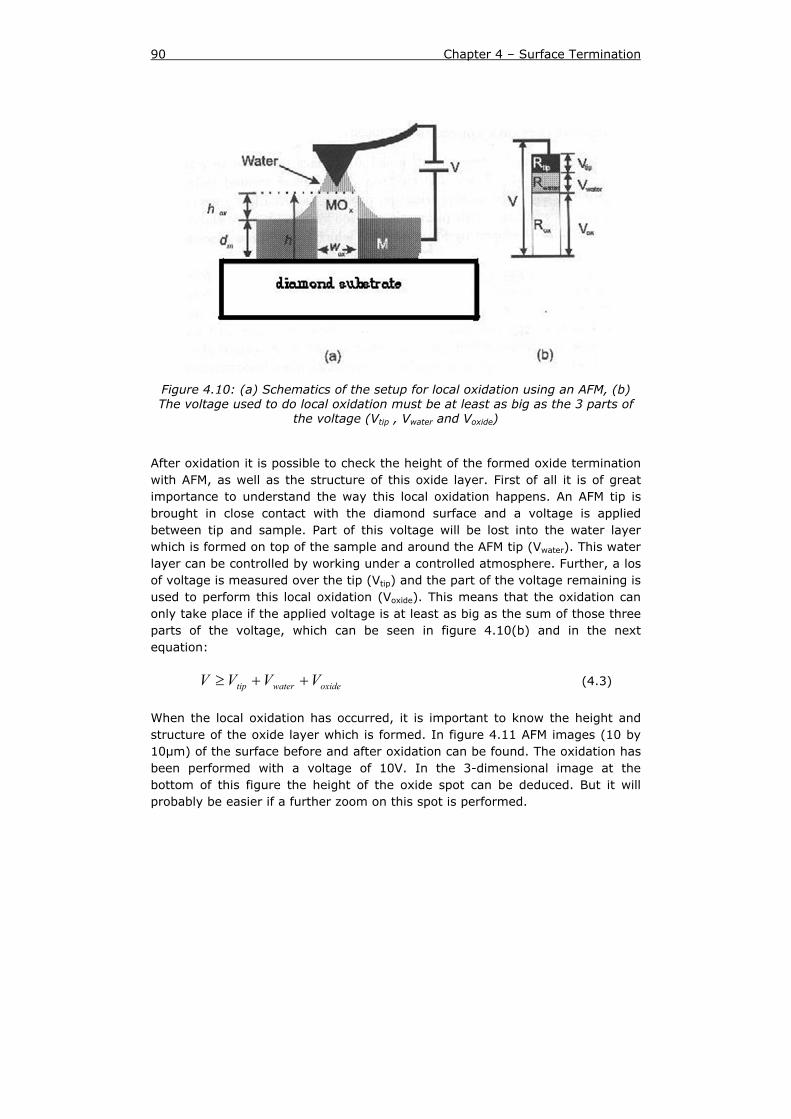
90 Chapter 4 – Surface Termination
Figure 4.10: (a) Schematics of the setup for local oxidation using an AFM, (b) The voltage used to do local oxidation must be at least as big as the 3 parts of
the voltage (Vtip , Vwater and Voxide)
After oxidation it is possible to check the height of the formed oxide termination with AFM, as well as the structure of this oxide layer. First of all it is of great importance to understand the way this local oxidation happens. An AFM tip is brought in close contact with the diamond surface and a voltage is applied between tip and sample. Part of this voltage will be lost into the water layer which is formed on top of the sample and around the AFM tip (Vwater). This water layer can be controlled by working under a controlled atmosphere. Further, a los of voltage is measured over the tip (Vtip) and the part of the voltage remaining is used to perform this local oxidation (Voxide). This means that the oxidation can only take place if the applied voltage is at least as big as the sum of those three parts of the voltage, which can be seen in figure 4.10(b) and in the next equation:
oxidewatertip VVVV ++≥ (4.3)
When the local oxidation has occurred, it is important to know the height and structure of the oxide layer which is formed. In figure 4.11 AFM images (10 by 10μm) of the surface before and after oxidation can be found. The oxidation has been performed with a voltage of 10V. In the 3-dimensional image at the bottom of this figure the height of the oxide spot can be deduced. But it will probably be easier if a further zoom on this spot is performed.
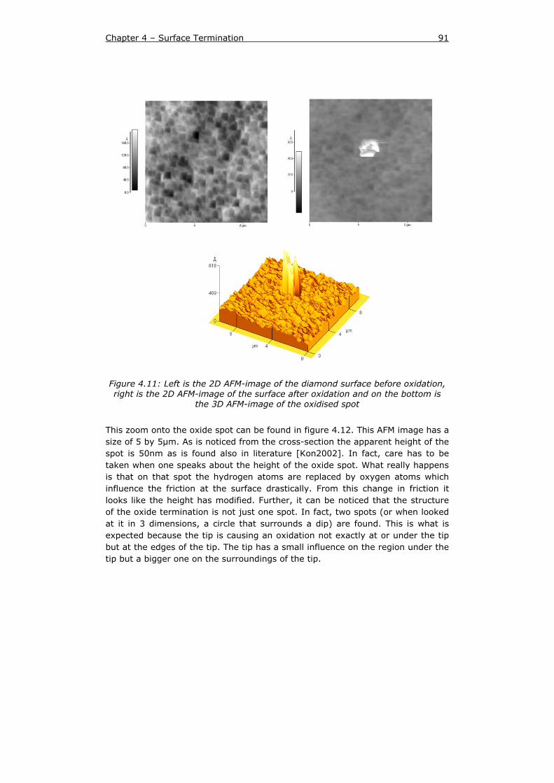
Chapter 4 – Surface Termination 91
Figure 4.11: Left is the 2D AFM-image of the diamond surface before oxidation, right is the 2D AFM-image of the surface after oxidation and on the bottom is
the 3D AFM-image of the oxidised spot
This zoom onto the oxide spot can be found in figure 4.12. This AFM image has a size of 5 by 5μm. As is noticed from the cross-section the apparent height of the spot is 50nm as is found also in literature [Kon2002]. In fact, care has to be taken when one speaks about the height of the oxide spot. What really happens is that on that spot the hydrogen atoms are replaced by oxygen atoms which influence the friction at the surface drastically. From this change in friction it looks like the height has modified. Further, it can be noticed that the structure of the oxide termination is not just one spot. In fact, two spots (or when looked at it in 3 dimensions, a circle that surrounds a dip) are found. This is what is expected because the tip is causing an oxidation not exactly at or under the tip but at the edges of the tip. The tip has a small influence on the region under the tip but a bigger one on the surroundings of the tip.
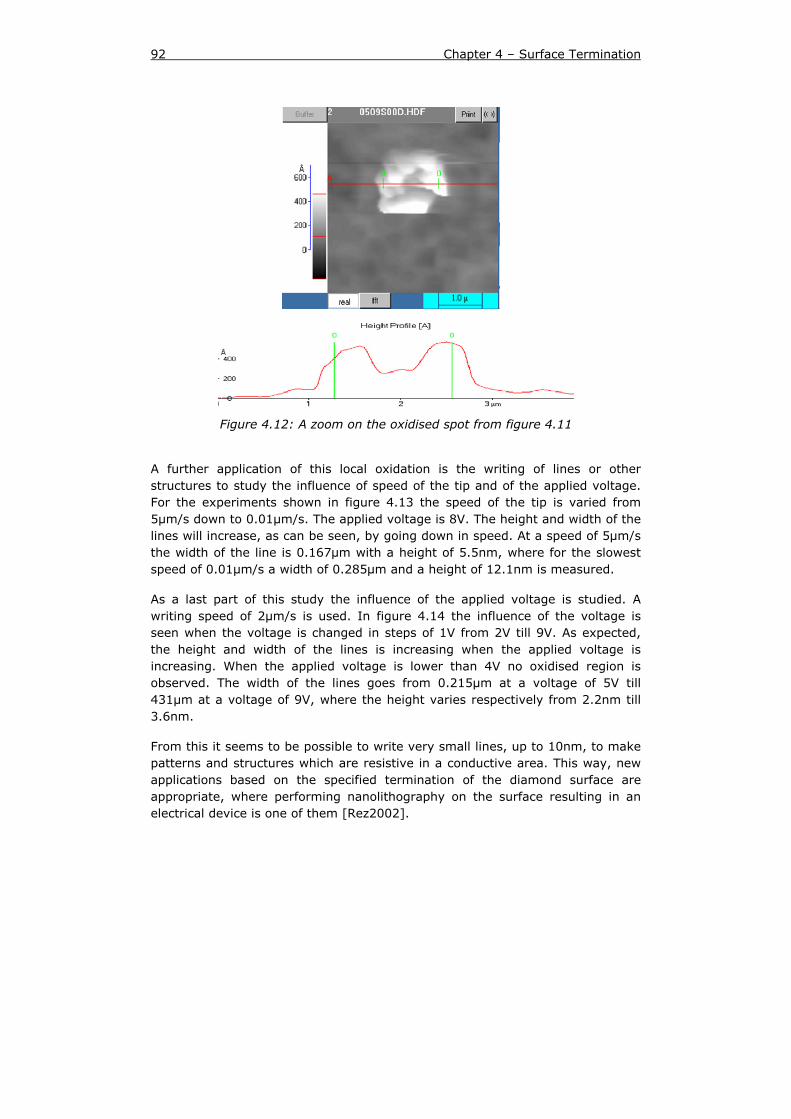
92 Chapter 4 – Surface Termination
Figure 4.12: A zoom on the oxidised spot from figure 4.11
A further application of this local oxidation is the writing of lines or other structures to study the influence of speed of the tip and of the applied voltage. For the experiments shown in figure 4.13 the speed of the tip is varied from 5μm/s down to 0.01μm/s. The applied voltage is 8V. The height and width of the lines will increase, as can be seen, by going down in speed. At a speed of 5μm/s the width of the line is 0.167μm with a height of 5.5nm, where for the slowest speed of 0.01μm/s a width of 0.285μm and a height of 12.1nm is measured.
As a last part of this study the influence of the applied voltage is studied. A writing speed of 2μm/s is used. In figure 4.14 the influence of the voltage is seen when the voltage is changed in steps of 1V from 2V till 9V. As expected, the height and width of the lines is increasing when the applied voltage is increasing. When the applied voltage is lower than 4V no oxidised region is observed. The width of the lines goes from 0.215μm at a voltage of 5V till 431μm at a voltage of 9V, where the height varies respectively from 2.2nm till 3.6nm.
From this it seems to be possible to write very small lines, up to 10nm, to make patterns and structures which are resistive in a conductive area. This way, new applications based on the specified termination of the diamond surface are appropriate, where performing nanolithography on the surface resulting in an electrical device is one of them [Rez2002].
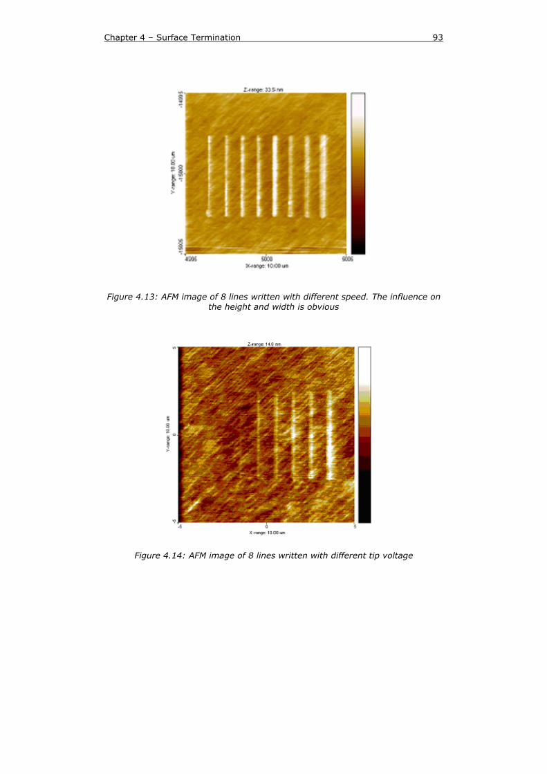
Chapter 4 – Surface Termination 93
Figure 4.13: AFM image of 8 lines written with different speed. The influence on the height and width is obvious
Figure 4.14: AFM image of 8 lines written with different tip voltage
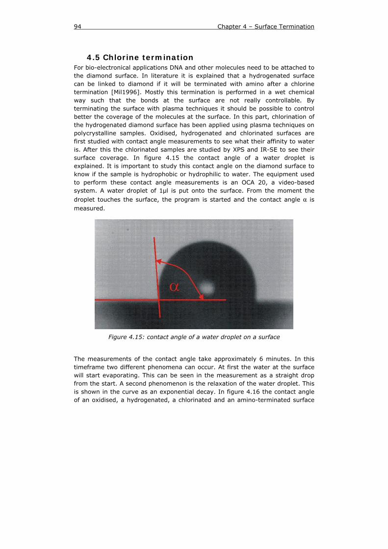
94 Chapter 4 – Surface Termination
4.5 Chlorine termination For bio-electronical applications DNA and other molecules need to be attached to the diamond surface. In literature it is explained that a hydrogenated surface can be linked to diamond if it will be terminated with amino after a chlorine termination [Mil1996]. Mostly this termination is performed in a wet chemical way such that the bonds at the surface are not really controllable. By terminating the surface with plasma techniques it should be possible to control better the coverage of the molecules at the surface. In this part, chlorination of the hydrogenated diamond surface has been applied using plasma techniques on polycrystalline samples. Oxidised, hydrogenated and chlorinated surfaces are first studied with contact angle measurements to see what their affinity to water is. After this the chlorinated samples are studied by XPS and IR-SE to see their surface coverage. In figure 4.15 the contact angle of a water droplet is explained. It is important to study this contact angle on the diamond surface to know if the sample is hydrophobic or hydrophilic to water. The equipment used to perform these contact angle measurements is an OCA 20, a video-based system. A water droplet of 1μl is put onto the surface. From the moment the
droplet touches the surface, the program is started and the contact angle α is measured.
Figure 4.15: contact angle of a water droplet on a surface
The measurements of the contact angle take approximately 6 minutes. In this timeframe two different phenomena can occur. At first the water at the surface will start evaporating. This can be seen in the measurement as a straight drop from the start. A second phenomenon is the relaxation of the water droplet. This is shown in the curve as an exponential decay. In figure 4.16 the contact angle of an oxidised, a hydrogenated, a chlorinated and an amino-terminated surface
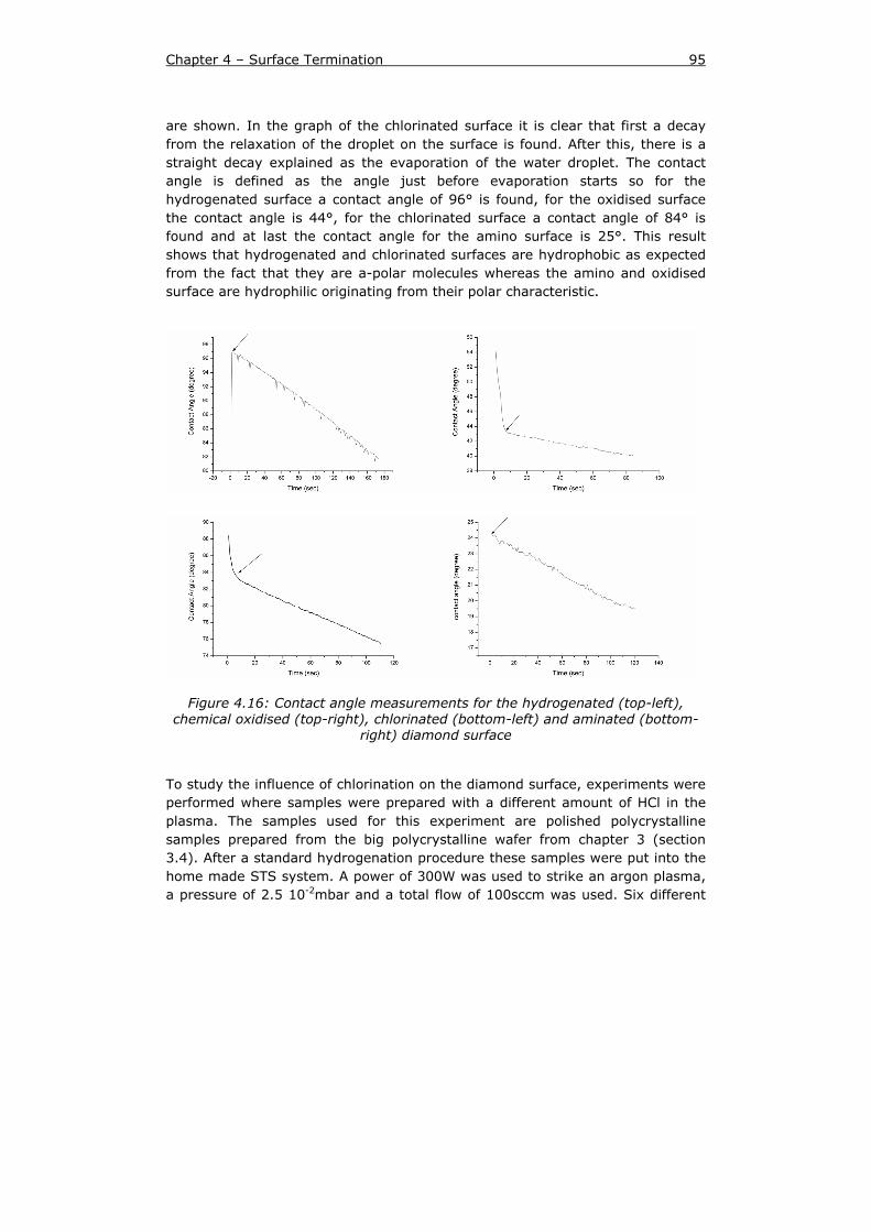
Chapter 4 – Surface Termination 95
are shown. In the graph of the chlorinated surface it is clear that first a decay from the relaxation of the droplet on the surface is found. After this, there is a straight decay explained as the evaporation of the water droplet. The contact angle is defined as the angle just before evaporation starts so for the hydrogenated surface a contact angle of 96° is found, for the oxidised surface the contact angle is 44°, for the chlorinated surface a contact angle of 84° is found and at last the contact angle for the amino surface is 25°. This result shows that hydrogenated and chlorinated surfaces are hydrophobic as expected from the fact that they are a-polar molecules whereas the amino and oxidised surface are hydrophilic originating from their polar characteristic.
Figure 4.16: Contact angle measurements for the hydrogenated (top-left), chemical oxidised (top-right), chlorinated (bottom-left) and aminated (bottom-
right) diamond surface
To study the influence of chlorination on the diamond surface, experiments were performed where samples were prepared with a different amount of HCl in the plasma. The samples used for this experiment are polished polycrystalline samples prepared from the big polycrystalline wafer from chapter 3 (section 3.4). After a standard hydrogenation procedure these samples were put into the home made STS system. A power of 300W was used to strike an argon plasma, a pressure of 2.5 10-2mbar and a total flow of 100sccm was used. Six different
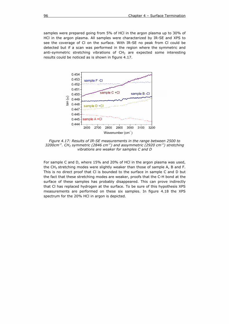
96 Chapter 4 – Surface Termination
samples were prepared going from 5% of HCl in the argon plasma up to 30% of HCl in the argon plasma. All samples were characterized by IR-SE and XPS to see the coverage of Cl on the surface. With IR-SE no peak from Cl could be detected but if a scan was performed in the region where the symmetric and anti-symmetric stretching vibrations of CH2 are expected some interesting results could be noticed as is shown in figure 4.17.
Figure 4.17: Results of IR-SE measurements in the range between 2500 to 3200cm-1. CH2 symmetric (2846 cm-1) and assymmetric (2920 cm-1) stretching
vibrations are weaker for samples C and D
For sample C and D, where 15% and 20% of HCl in the argon plasma was used, the CH2 stretching modes were slightly weaker than those of sample A, B and F. This is no direct proof that Cl is bounded to the surface in sample C and D but the fact that these stretching modes are weaker, proofs that the C-H bond at the surface of these samples has probably disappeared. This can prove indirectly that Cl has replaced hydrogen at the surface. To be sure of this hypothesis XPS measurements are performed on these six samples. In figure 4.18 the XPS spectrum for the 20% HCl in argon is depicted.
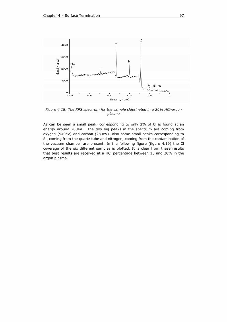
Chapter 4 – Surface Termination 97
Figure 4.18: The XPS spectrum for the sample chlorinated in a 20% HCl-argon plasma
As can be seen a small peak, corresponding to only 2% of Cl is found at an energy around 200eV. The two big peaks in the spectrum are coming from oxygen (540eV) and carbon (280eV). Also some small peaks corresponding to Si, coming from the quartz tube and nitrogen, coming from the contamination of the vacuum chamber are present. In the following figure (figure 4.19) the Cl coverage of the six different samples is plotted. It is clear from these results that best results are received at a HCl percentage between 15 and 20% in the argon plasma.
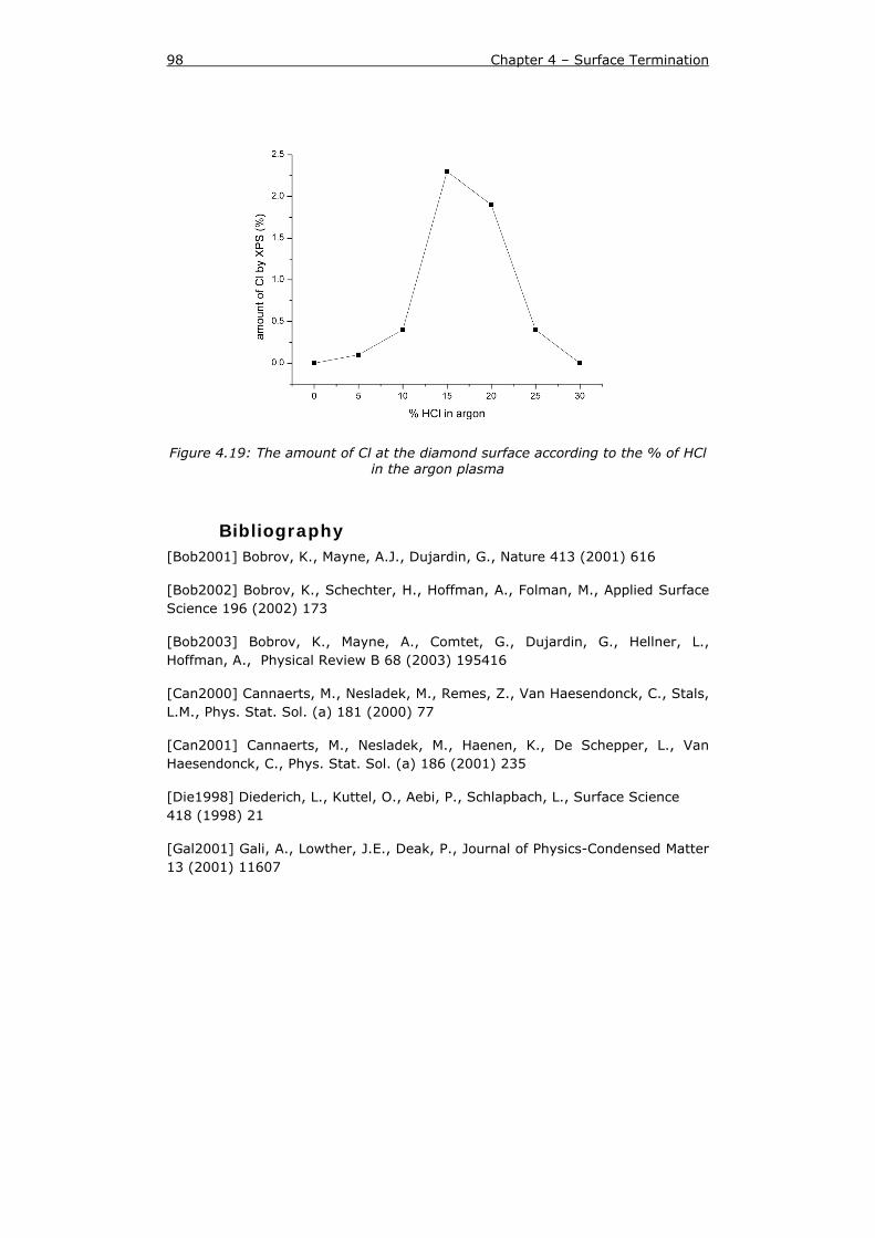
98 Chapter 4 – Surface Termination
Figure 4.19: The amount of Cl at the diamond surface according to the % of HCl in the argon plasma
Bibliography [Bob2001] Bobrov, K., Mayne, A.J., Dujardin, G., Nature 413 (2001) 616
[Bob2002] Bobrov, K., Schechter, H., Hoffman, A., Folman, M., Applied Surface Science 196 (2002) 173
[Bob2003] Bobrov, K., Mayne, A., Comtet, G., Dujardin, G., Hellner, L., Hoffman, A., Physical Review B 68 (2003) 195416
[Can2000] Cannaerts, M., Nesladek, M., Remes, Z., Van Haesendonck, C., Stals, L.M., Phys. Stat. Sol. (a) 181 (2000) 77
[Can2001] Cannaerts, M., Nesladek, M., Haenen, K., De Schepper, L., Van Haesendonck, C., Phys. Stat. Sol. (a) 186 (2001) 235
[Die1998] Diederich, L., Kuttel, O., Aebi, P., Schlapbach, L., Surface Science 418 (1998) 21
[Gal2001] Gali, A., Lowther, J.E., Deak, P., Journal of Physics-Condensed Matter 13 (2001) 11607
Chapter 4 – Surface Termination 99
[Gar2003] Garrido, J.A., Nebel, C.E., Todt, R., Rosel, G., Amann, M.C., Stutzmann, M., Snidero, E., Bergonzo, P., Applied Physics Letters 82 (2003) 988
[Kaw1996] Kawarada, H., Surface Science Reports 26 (1996) 205
[Kon2002] Kondo, T., Yanagisawa, M., Jiang, L., Tryk, T.A., Fujishima, A., Diam. Relat. Mater. 11 (2002) 1788
[Mai2000] Maier, F., Riedel, M., Mantel, B., Ristein, J., Ley, L., Physical Review Letters 85 (2000) 3472
[Mil1996] Miller, J.B., Brown, D.W., Langmuir 12 (1996) 5809
[Rez2002] Rezek, B., Garrido, J.A., Stutzmann, M., Nebel, C.E., Snidero, E., Bergonzo, P., Phys. Stat. Sol. (a) 193 (2002) 523
[Rie2004] Riedel, M., Ristein, J., Ley, L., Physical Review B 69 (2004) 125338
[Ris2001] Ristein, J., Maier, F., Riedel, M., Stammer, M., Ley, L., Diam. Relat. Mater. 10 (2001) 416
[Zhe2001] Zheng, J.X., Xie, X.N., Wee, A.T.S., Loh, K.P., Diamond and Related Materials 10 (2001) 500

Diamond is not forever
Because diamond is not at equilibrium
So we have to keep the pressure
--- Milos Nesladek ---
Chapter 5 - Time-of-Flight
In this chapter, the Time-of-Flight technique is described, used to study the transport properties of diamond layers. First an introduction is given on how to prepare the samples and the experimental set-up. After this 3 major parts deal with different measurements. The first is closely related to chapter 4. The surface of our diamond samples is treated with an hydrogen or an oxygen plasma and by measuring the ToF it is examined if there is any influence on the mobility and transit of charge carriers. In a second part, the temperature dependent mobility is measured and it is discussed what the limiting factors for the charge carrier transport are. In a third part the influence of contact preparation is examined. When contacts are prepared on oxidised diamond surfaces by two different techniques, the influence on the charge trapping at the contacts is discussed. In a last part we discuss electroluminescence from the samples prepared for ToF measurements.
5.1 Preparation Using Time-of-Flight measurements it is important that several conditions of the samples are met. First of all, diamond samples should be not conductive at all. Being too conductive screening of the movement of charge happens. Further, the diamond should be freestanding and should therefore have a specific thickness. The distance the carriers will travel should be known which means that all charge should be created at the close proximity of the illuminated contact. This is fulfilled for just above band gap radiation which has a penetration depth of only ~1μm in diamond. As the freestanding diamond samples have a minimum thickness of around 400μm it is clear that this penetration depth can be neglected. Further, good contacts should be prepared where the front contact should be semi-transparent for the laser pulse. The back contact can be thicker but should provide a good transfer of the signal to the set-up. At last the set-up should be tuned with lenses and filters such that only just above bandgap light (218nm) is reaching the diamond surface to restrict the influence of other light waves.
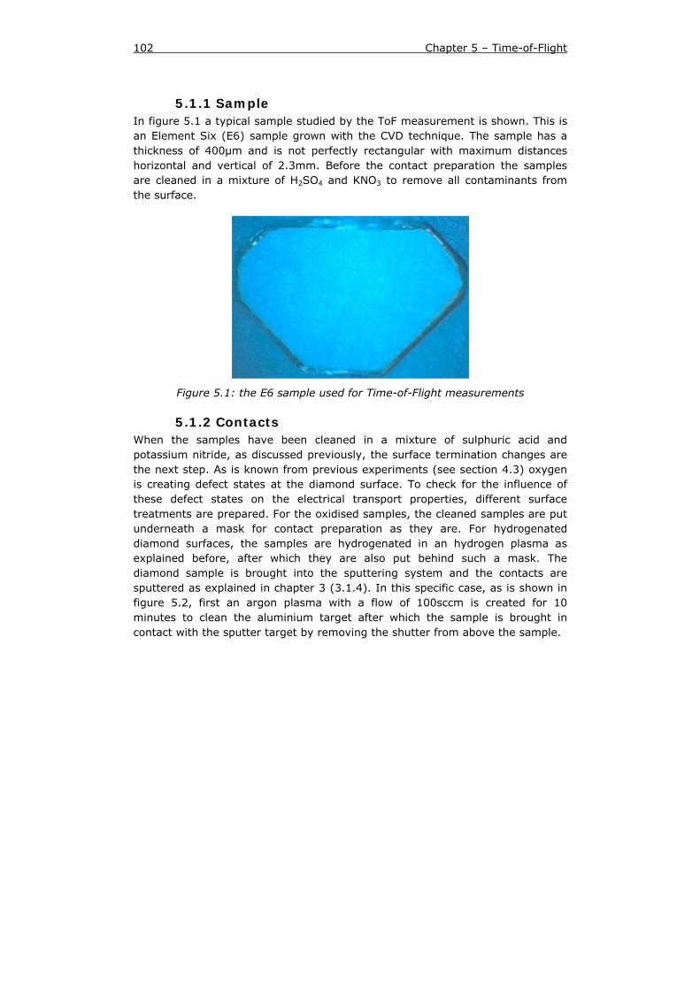
102 Chapter 5 – Time-of-Flight
5.1.1 Sample In figure 5.1 a typical sample studied by the ToF measurement is shown. This is an Element Six (E6) sample grown with the CVD technique. The sample has a thickness of 400μm and is not perfectly rectangular with maximum distances horizontal and vertical of 2.3mm. Before the contact preparation the samples are cleaned in a mixture of H2SO4 and KNO3 to remove all contaminants from the surface.
Figure 5.1: the E6 sample used for Time-of-Flight measurements
5.1.2 Contacts When the samples have been cleaned in a mixture of sulphuric acid and potassium nitride, as discussed previously, the surface termination changes are the next step. As is known from previous experiments (see section 4.3) oxygen is creating defect states at the diamond surface. To check for the influence of these defect states on the electrical transport properties, different surface treatments are prepared. For the oxidised samples, the cleaned samples are put underneath a mask for contact preparation as they are. For hydrogenated diamond surfaces, the samples are hydrogenated in an hydrogen plasma as explained before, after which they are also put behind such a mask. The diamond sample is brought into the sputtering system and the contacts are sputtered as explained in chapter 3 (3.1.4). In this specific case, as is shown in figure 5.2, first an argon plasma with a flow of 100sccm is created for 10 minutes to clean the aluminium target after which the sample is brought in contact with the sputter target by removing the shutter from above the sample.
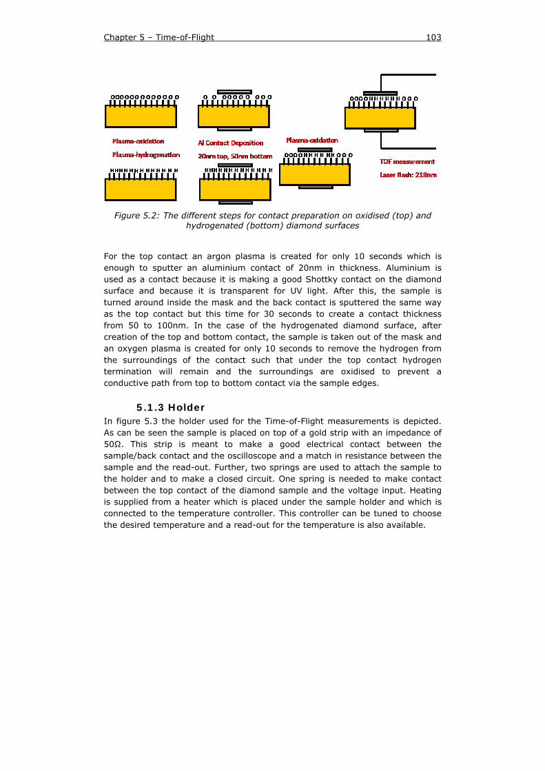
Chapter 5 – Time-of-Flight 103
Figure 5.2: The different steps for contact preparation on oxidised (top) and hydrogenated (bottom) diamond surfaces
For the top contact an argon plasma is created for only 10 seconds which is enough to sputter an aluminium contact of 20nm in thickness. Aluminium is used as a contact because it is making a good Shottky contact on the diamond surface and because it is transparent for UV light. After this, the sample is turned around inside the mask and the back contact is sputtered the same way as the top contact but this time for 30 seconds to create a contact thickness from 50 to 100nm. In the case of the hydrogenated diamond surface, after creation of the top and bottom contact, the sample is taken out of the mask and an oxygen plasma is created for only 10 seconds to remove the hydrogen from the surroundings of the contact such that under the top contact hydrogen termination will remain and the surroundings are oxidised to prevent a conductive path from top to bottom contact via the sample edges.
5.1.3 Holder In figure 5.3 the holder used for the Time-of-Flight measurements is depicted. As can be seen the sample is placed on top of a gold strip with an impedance of 50Ω. This strip is meant to make a good electrical contact between the sample/back contact and the oscilloscope and a match in resistance between the sample and the read-out. Further, two springs are used to attach the sample to the holder and to make a closed circuit. One spring is needed to make contact between the top contact of the diamond sample and the voltage input. Heating is supplied from a heater which is placed under the sample holder and which is connected to the temperature controller. This controller can be tuned to choose the desired temperature and a read-out for the temperature is also available.
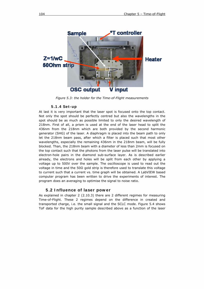
104 Chapter 5 – Time-of-Flight
Figure 5.3: the holder for the Time-of-Flight measurements
5.1.4 Set-up At last it is very important that the laser spot is focused onto the top contact. Not only the spot should be perfectly centred but also the wavelengths in the spot should be as much as possible limited to only the desired wavelength of 218nm. First of all, a prism is used at the end of the laser head to split the 436nm from the 218nm which are both provided by the second harmonic generator (SHG) of the laser. A diaphragm is placed into the beam path to only let the 218nm beam pass, after which a filter is placed such that most other wavelengths, especially the remaining 436nm in the 218nm beam, will be fully blocked. Than, the 218nm beam with a diameter of less than 2mm is focused on the top contact such that the photons from the laser pulse will be translated into electron-hole pairs in the diamond sub-surface layer. As is described earlier already, the electrons and holes will be split from each other by applying a voltage up to 500V over the sample. The oscilloscope is used to read out the voltage in time and the 50Ω gold strip is therefore used to translate this voltage to current such that a current vs. time graph will be obtained. A LabVIEW based computer program has been written to drive the experiments of interest. The program does an averaging to optimise the signal to noise ratio.
5.2 Influence of laser power As explained in chapter 2 (2.10.3) there are 2 different regimes for measuring Time-of-Flight. These 2 regimes depend on the difference in created and transported charge, i.e. the small signal and the SCLC mode. Figure 5.4 shows ToF data for the high purity sample described above as a function of the laser

Chapter 5 – Time-of-Flight 105
intensity expressed in the power of the IR (1024 μm) YAG beam. From figure 5.4 it can be established that a clear non-dispersive signal approaching an ideal rectangular shape can be found for the transit of electrons and holes for low laser intensity. By increasing the laser intensity we reach the SCLC conditions as indicated by a dotted line in figure 5.4. In order to determine the charge carrier mobility μ0 at low fields and for the small signal case we have fitted the experimental data with the formula (5.1).
satvE0
0
1μμ
μ+
= (5.1)
The parameters μ0 and saturation velocity (vsat) were adjusted to match the slope (see section 5.3 fig 5.6). Upon increasing the laser intensity the shape of the transient changes significantly and a “cusp” characteristic for the SCLC mode appears. This feature is related to the so-called extraction time [Piv2005, Isb2004], which is usually shorter than the transit time by a relation where β as coefficient is about 0.787 [Isb2004].

106 Chapter 5 – Time-of-Flight
Figure 5.4: Influence of laser power on the ToF measurements for electrons and holes
Chapter 5 – Time-of-Flight 107
The mobility determined from the space charge limited current (SCLC) mode is than calculated using numerical fitting based on the following equation (5.2).
trE tt .β= (5.2)
This fitting yields a value of 2050cm²/Vs for electrons and 2250cm²/Vs for holes at room temperature. These values correspond very well to the data obtained for IIa diamond with a difference of ± 200cm²/Vs. A nearly perfect signal with no trapping is visible. To our opinion the main difference between IIa and CVD diamond samples comes from the precision for the determination of the transit
time ttr, which is about 10-15 % due to the dispersive character of the transport
in IIa diamond. The transit time ttr is indicated by arrows in figure 5.4. As
discussed in the literature, several definitions of ttr can be found, one of them is that ttr is defined as a time during which the photocurrent drops to 50% of its value after the laser shot charge generation [Mai1991, Neb1997]. This definition of the transit time ttr is related to a movement of the main weight of the laser generated charge parcel, transported through the sample. However, this definition can only be used in the case of non-dispersive transport i.e by an absence of the charge trapping which delays by trapping and re-emission events the arrival of charge to the collecting electrode. In this case part of the charge is trapped just after the laser pulse and the change in the slope in the log(I)- log(t) plot indicates the arrival of the fastest carriers to the collecting electrode. Such transit time is directly related to the microscopic drift mobility, defined as a time needed for the fastest carriers to traverse the sample from the front to the back electrode without any trapping. However, as we will show in this thesis, the main differences in the determination of the electron and hole drift mobility comes from the changes in the electric field profiles in the sample. However for this diamond sample the value for the electron mobility is slightly lower as the hole mobility. These values were used to determine the coefficient β from equation 5.2 and using the experimentally measured extraction time tE, which yields 0.85 for β.
Edt
hetr .
.
,μβ
= (5.3)
This suggests that the mechanism of the charge trapping at the contacts for low electric field deviates slightly from the results presented in [Isb2004]. This is believed to be mainly affected by charge trapping at the contacts, which is changing the electric field profile.
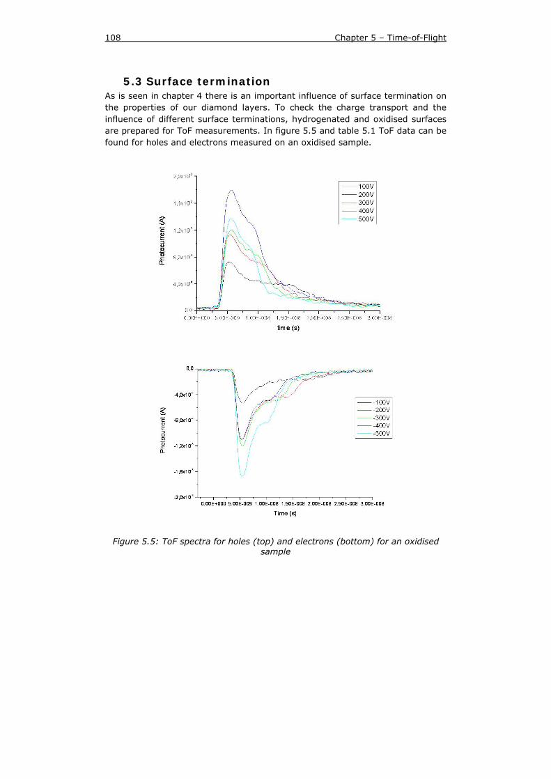
108 Chapter 5 – Time-of-Flight
5.3 Surface termination As is seen in chapter 4 there is an important influence of surface termination on the properties of our diamond layers. To check the charge transport and the influence of different surface terminations, hydrogenated and oxidised surfaces are prepared for ToF measurements. In figure 5.5 and table 5.1 ToF data can be found for holes and electrons measured on an oxidised sample.
Figure 5.5: ToF spectra for holes (top) and electrons (bottom) for an oxidised sample
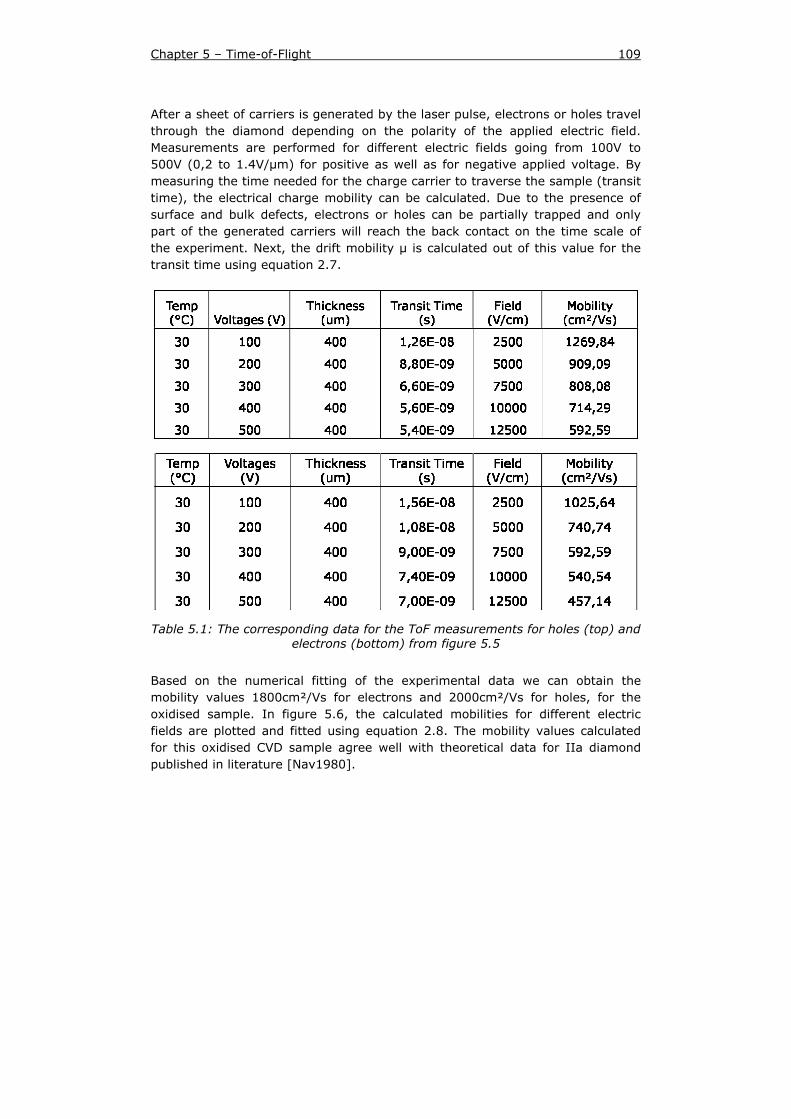
Chapter 5 – Time-of-Flight 109
After a sheet of carriers is generated by the laser pulse, electrons or holes travel through the diamond depending on the polarity of the applied electric field. Measurements are performed for different electric fields going from 100V to 500V (0,2 to 1.4V/μm) for positive as well as for negative applied voltage. By measuring the time needed for the charge carrier to traverse the sample (transit time), the electrical charge mobility can be calculated. Due to the presence of surface and bulk defects, electrons or holes can be partially trapped and only part of the generated carriers will reach the back contact on the time scale of the experiment. Next, the drift mobility μ is calculated out of this value for the transit time using equation 2.7.
Table 5.1: The corresponding data for the ToF measurements for holes (top) and electrons (bottom) from figure 5.5
Based on the numerical fitting of the experimental data we can obtain the mobility values 1800cm²/Vs for electrons and 2000cm²/Vs for holes, for the oxidised sample. In figure 5.6, the calculated mobilities for different electric fields are plotted and fitted using equation 2.8. The mobility values calculated for this oxidised CVD sample agree well with theoretical data for IIa diamond published in literature [Nav1980].
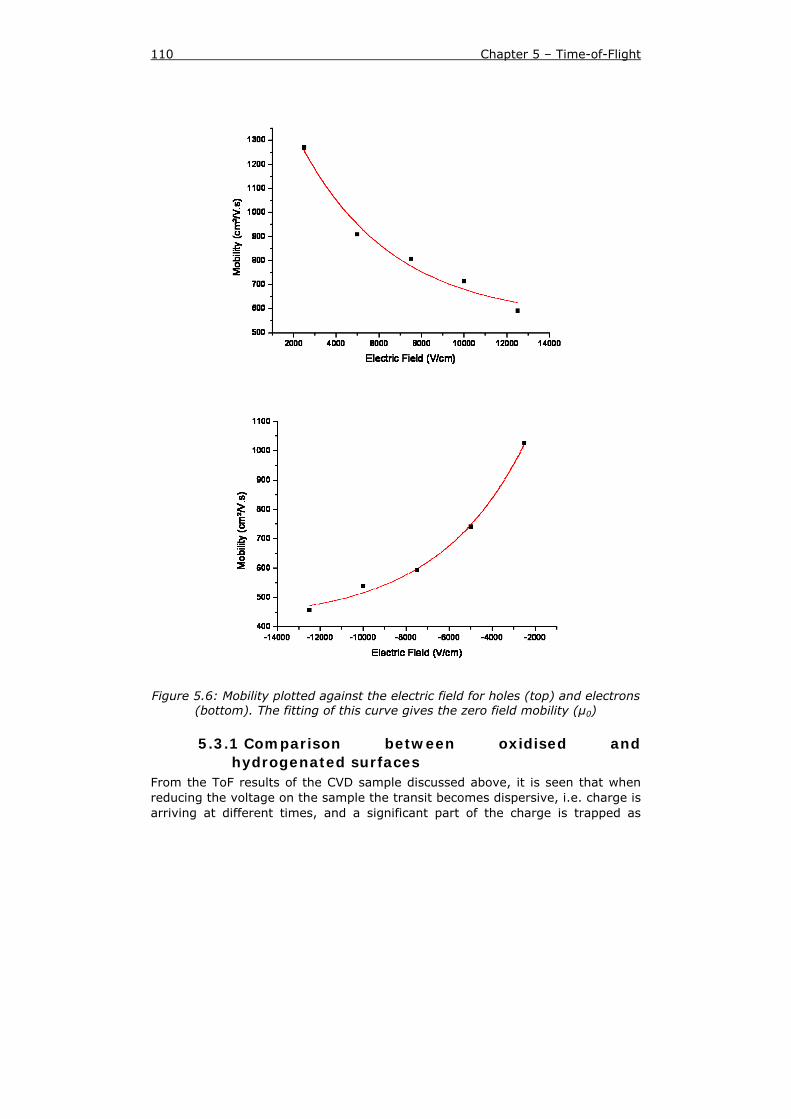
110 Chapter 5 – Time-of-Flight
Figure 5.6: Mobility plotted against the electric field for holes (top) and electrons (bottom). The fitting of this curve gives the zero field mobility (μ0)
5.3.1 Comparison between oxidised and hydrogenated surfaces
From the ToF results of the CVD sample discussed above, it is seen that when reducing the voltage on the sample the transit becomes dispersive, i.e. charge is arriving at different times, and a significant part of the charge is trapped as
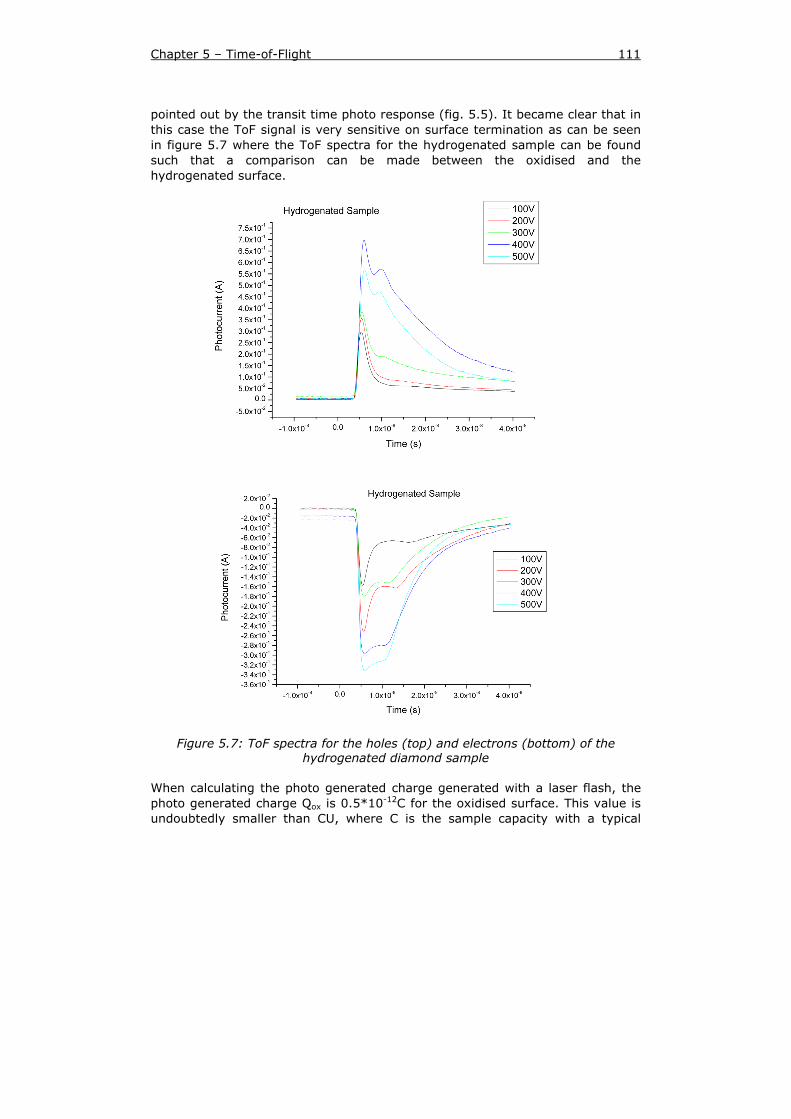
Chapter 5 – Time-of-Flight 111
pointed out by the transit time photo response (fig. 5.5). It became clear that in this case the ToF signal is very sensitive on surface termination as can be seen in figure 5.7 where the ToF spectra for the hydrogenated sample can be found such that a comparison can be made between the oxidised and the hydrogenated surface.
Figure 5.7: ToF spectra for the holes (top) and electrons (bottom) of the hydrogenated diamond sample
When calculating the photo generated charge generated with a laser flash, the photo generated charge Qox is 0.5*10-12C for the oxidised surface. This value is undoubtedly smaller than CU, where C is the sample capacity with a typical
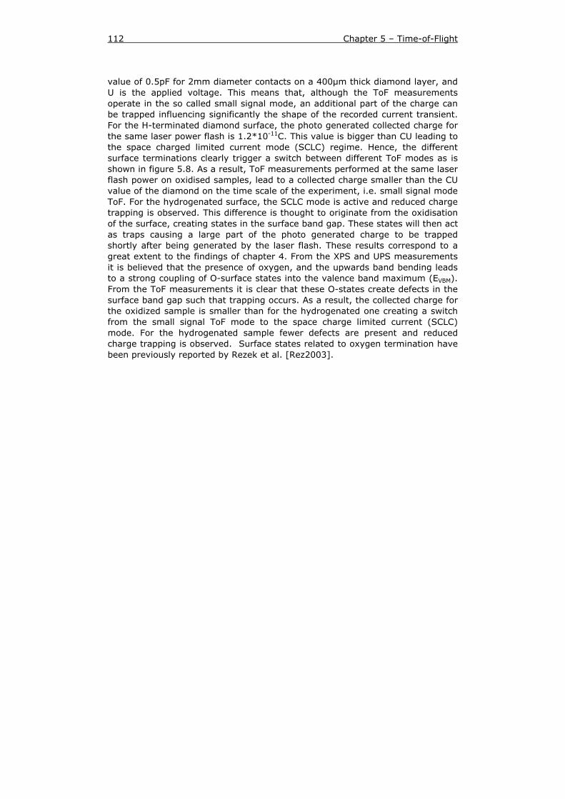
112 Chapter 5 – Time-of-Flight
value of 0.5pF for 2mm diameter contacts on a 400μm thick diamond layer, and U is the applied voltage. This means that, although the ToF measurements operate in the so called small signal mode, an additional part of the charge can be trapped influencing significantly the shape of the recorded current transient. For the H-terminated diamond surface, the photo generated collected charge for the same laser power flash is 1.2*10-11C. This value is bigger than CU leading to the space charged limited current mode (SCLC) regime. Hence, the different surface terminations clearly trigger a switch between different ToF modes as is shown in figure 5.8. As a result, ToF measurements performed at the same laser flash power on oxidised samples, lead to a collected charge smaller than the CU value of the diamond on the time scale of the experiment, i.e. small signal mode ToF. For the hydrogenated surface, the SCLC mode is active and reduced charge trapping is observed. This difference is thought to originate from the oxidisation of the surface, creating states in the surface band gap. These states will then act as traps causing a large part of the photo generated charge to be trapped shortly after being generated by the laser flash. These results correspond to a great extent to the findings of chapter 4. From the XPS and UPS measurements it is believed that the presence of oxygen, and the upwards band bending leads to a strong coupling of O-surface states into the valence band maximum (EVBM). From the ToF measurements it is clear that these O-states create defects in the surface band gap such that trapping occurs. As a result, the collected charge for the oxidized sample is smaller than for the hydrogenated one creating a switch from the small signal ToF mode to the space charge limited current (SCLC) mode. For the hydrogenated sample fewer defects are present and reduced charge trapping is observed. Surface states related to oxygen termination have been previously reported by Rezek et al. [Rez2003].
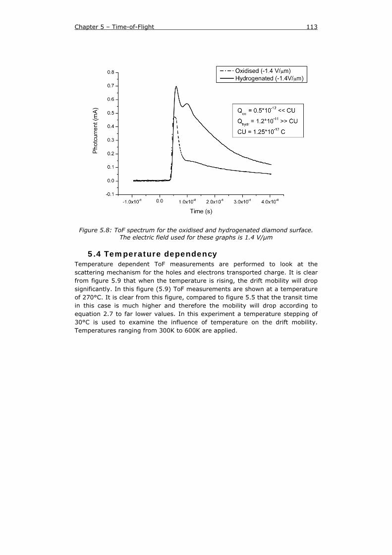
Chapter 5 – Time-of-Flight 113
Figure 5.8: ToF spectrum for the oxidised and hydrogenated diamond surface. The electric field used for these graphs is 1.4 V/µm
5.4 Temperature dependency Temperature dependent ToF measurements are performed to look at the scattering mechanism for the holes and electrons transported charge. It is clear from figure 5.9 that when the temperature is rising, the drift mobility will drop significantly. In this figure (5.9) ToF measurements are shown at a temperature of 270°C. It is clear from this figure, compared to figure 5.5 that the transit time in this case is much higher and therefore the mobility will drop according to equation 2.7 to far lower values. In this experiment a temperature stepping of 30°C is used to examine the influence of temperature on the drift mobility. Temperatures ranging from 300K to 600K are applied.
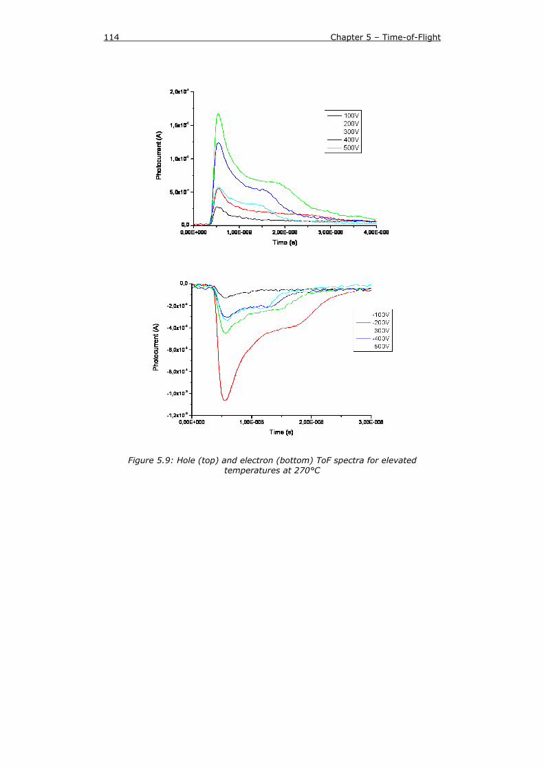
114 Chapter 5 – Time-of-Flight
Figure 5.9: Hole (top) and electron (bottom) ToF spectra for elevated temperatures at 270°C
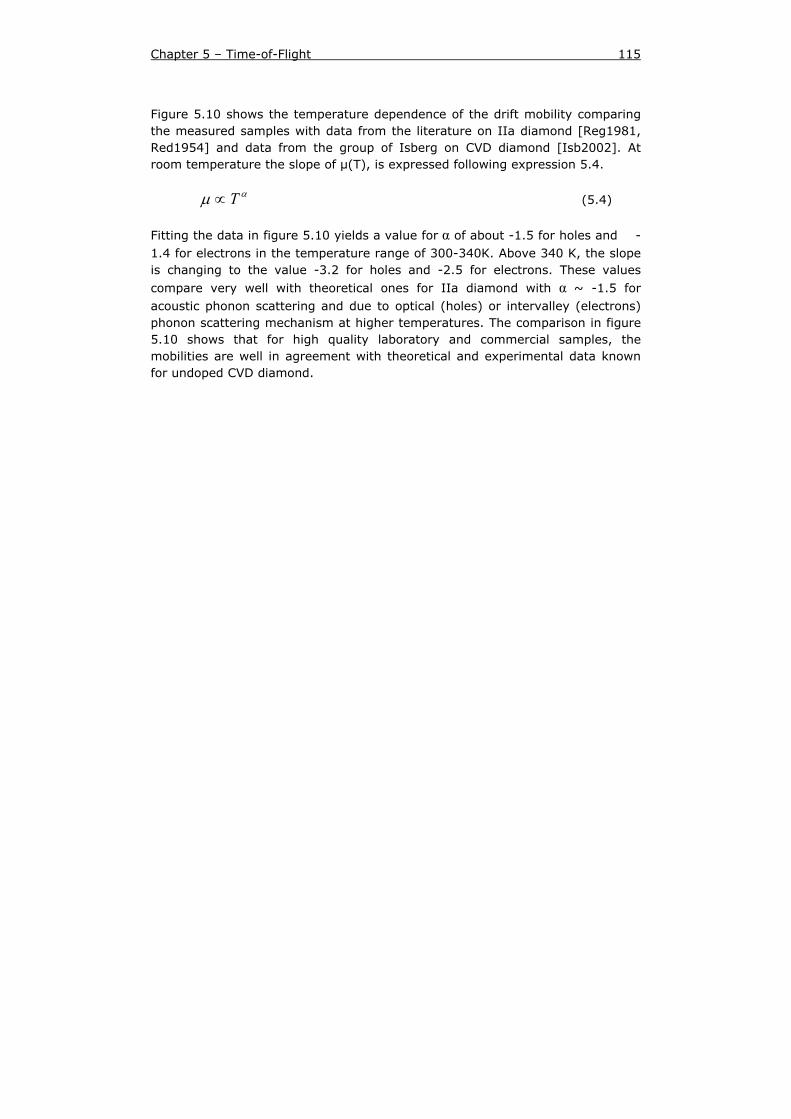
Chapter 5 – Time-of-Flight 115
Figure 5.10 shows the temperature dependence of the drift mobility comparing the measured samples with data from the literature on IIa diamond [Reg1981, Red1954] and data from the group of Isberg on CVD diamond [Isb2002]. At room temperature the slope of μ(T), is expressed following expression 5.4.
αμ T∝ (5.4)
Fitting the data in figure 5.10 yields a value for α of about -1.5 for holes and -1.4 for electrons in the temperature range of 300-340K. Above 340 K, the slope is changing to the value -3.2 for holes and -2.5 for electrons. These values
compare very well with theoretical ones for IIa diamond with α ~ -1.5 for acoustic phonon scattering and due to optical (holes) or intervalley (electrons) phonon scattering mechanism at higher temperatures. The comparison in figure 5.10 shows that for high quality laboratory and commercial samples, the mobilities are well in agreement with theoretical and experimental data known for undoped CVD diamond.
116 Chapter 5 – Time-of-Flight
Figure 5.10: The temperature dependence of the hole (top) and electron
(bottom) mobility for our samples plotted in comparison with the published data
Chapter 5 – Time-of-Flight 117
5.5 Contact influence Another issue related to the charge transport properties are local electric fields induced by the charge trapping at bulk and surface defects. Especially the diamond-contact interface can play a major role in inducing extra charge trapping when not appropriately prepared. Therefore, contacts are prepared on two different manners. The contact preparations, i.e. sputtering and evaporation are described above. Figure 5.11 shows the ToF spectra for electrons and holes obtained with a voltage of 0.3V/μm on a sample with Al contacts prepared with the two different methods as described above. In a material where little or no trapping occurs, the measured current is constant when the electron cloud is travelling at constant drift velocity (vd) through the sample, only to decrease when the first electrons have traversed the complete sample.
satee
sat
e
dtr v
dU
dEv
E
dvdt +=
+==
μμ
μ21
(5.5)
In this equation ttr is the transit time, d is the thickness, μ the mobility, U the applied voltage, E = U/d the corresponding electric field, vd the drift velocity and vsat the saturation velocity. Fitting the experimental data with equations 5.6 and 5.7 the mobility and the saturation velocity can be determined.
ad 2
0 =μ (5.6)
bdvsat = (5.7)
As can be seen from figure 5.11, the ToF spectrum obtained with sputtered contacts corresponds perfectly to the ideal situation just described: no trapping occurs and all the exited electrons reach the back contact. On the other hand, the ToF spectrum taken with evaporated contacts looks quite different. Part of the electrons seems to disappear from the current signal immediately after their creation so that only part of the charge traverses the complete 400µm of the sample. As the same sample was used for both measurements, i.e. the bulk properties are identical in both experiments, this behaviour can only be explained by the creation of surface states at the diamond-contact interface acting as charge trapping states. These states are responsible for the trapping of part of the electrons, influencing the electrical field and resulting in a very differently shaped ToF spectrum. When the polarity of the voltage pulse is reversed, holes in stead of electrons are travelling through the sample from top to back contact. The same behaviour for holes can be found as for electrons as also can be seen in the inset of figure 5.11. For the sputtered contact a textbook-like ToF spectrum can be noticed where for the evaporated contact a peak corresponding to trapping at the surface is found.
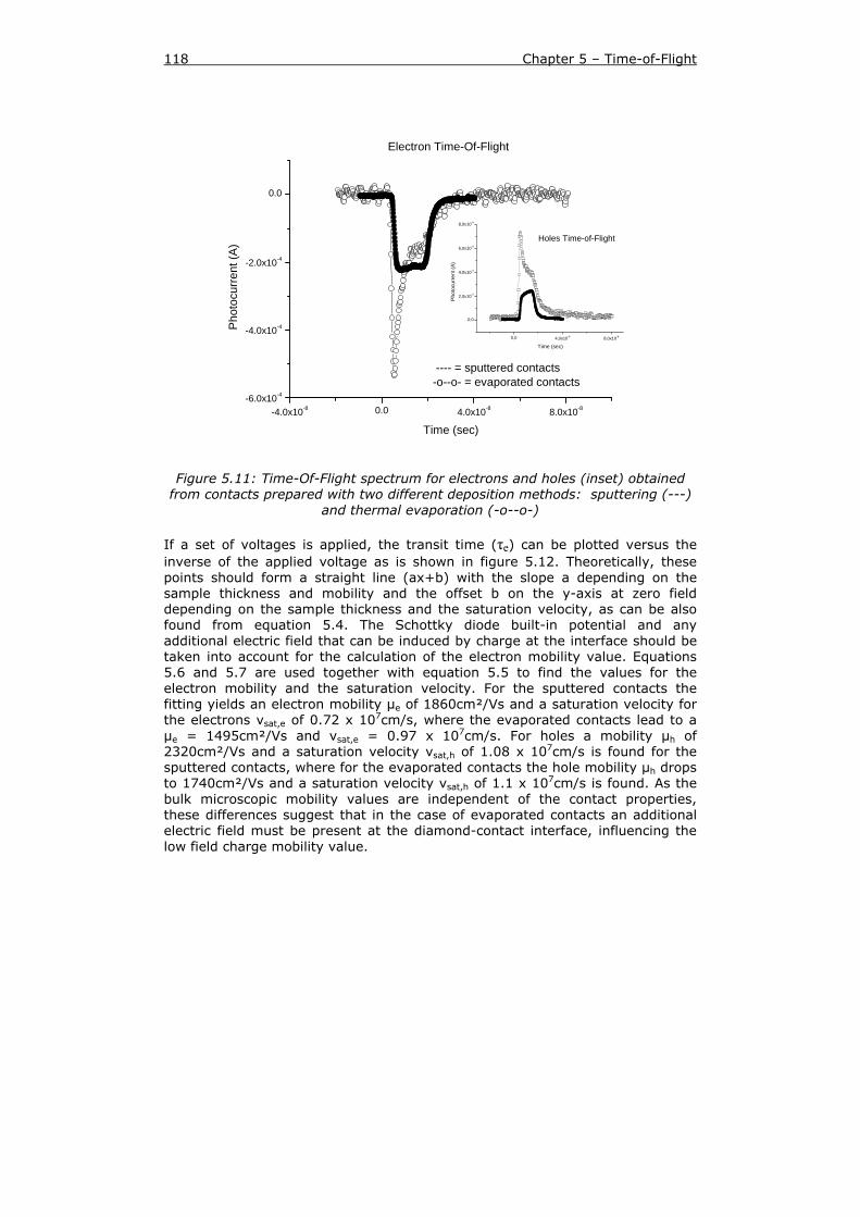
118 Chapter 5 – Time-of-Flight
-4.0x10⁻⁸ 0.0 4.0x10⁻⁸ 8.0x10⁻⁸-6.0x10⁻⁴
-4.0x10⁻⁴
-2.0x10⁻⁴
0.0
Holes Time-of-Flight
0,0 4,0x10⁻⁸ 8,0x10⁻⁸
0,0
2,0x10⁻⁴
4,0x10⁻⁴
6,0x10⁻⁴
8,0x10⁻⁴
Phot
ocur
rent
(A)
Time (sec)
---- = sputtered contacts-o--o- = evaporated contacts
Pho
tocu
rren
t (A
)
Time (sec)
Electron Time-Of-Flight
Figure 5.11: Time-Of-Flight spectrum for electrons and holes (inset) obtained from contacts prepared with two different deposition methods: sputtering (---)
and thermal evaporation (-o--o-) If a set of voltages is applied, the transit time (τe) can be plotted versus the inverse of the applied voltage as is shown in figure 5.12. Theoretically, these points should form a straight line (ax+b) with the slope a depending on the sample thickness and mobility and the offset b on the y-axis at zero field depending on the sample thickness and the saturation velocity, as can be also found from equation 5.4. The Schottky diode built-in potential and any additional electric field that can be induced by charge at the interface should be taken into account for the calculation of the electron mobility value. Equations 5.6 and 5.7 are used together with equation 5.5 to find the values for the electron mobility and the saturation velocity. For the sputtered contacts the fitting yields an electron mobility μe of 1860cm²/Vs and a saturation velocity for the electrons vsat,e of 0.72 x 107cm/s, where the evaporated contacts lead to a μe = 1495cm²/Vs and vsat,e = 0.97 x 107cm/s. For holes a mobility μh of 2320cm²/Vs and a saturation velocity vsat,h of 1.08 x 107cm/s is found for the sputtered contacts, where for the evaporated contacts the hole mobility μh drops to 1740cm²/Vs and a saturation velocity vsat,h of 1.1 x 107cm/s is found. As the bulk microscopic mobility values are independent of the contact properties, these differences suggest that in the case of evaporated contacts an additional electric field must be present at the diamond-contact interface, influencing the low field charge mobility value.
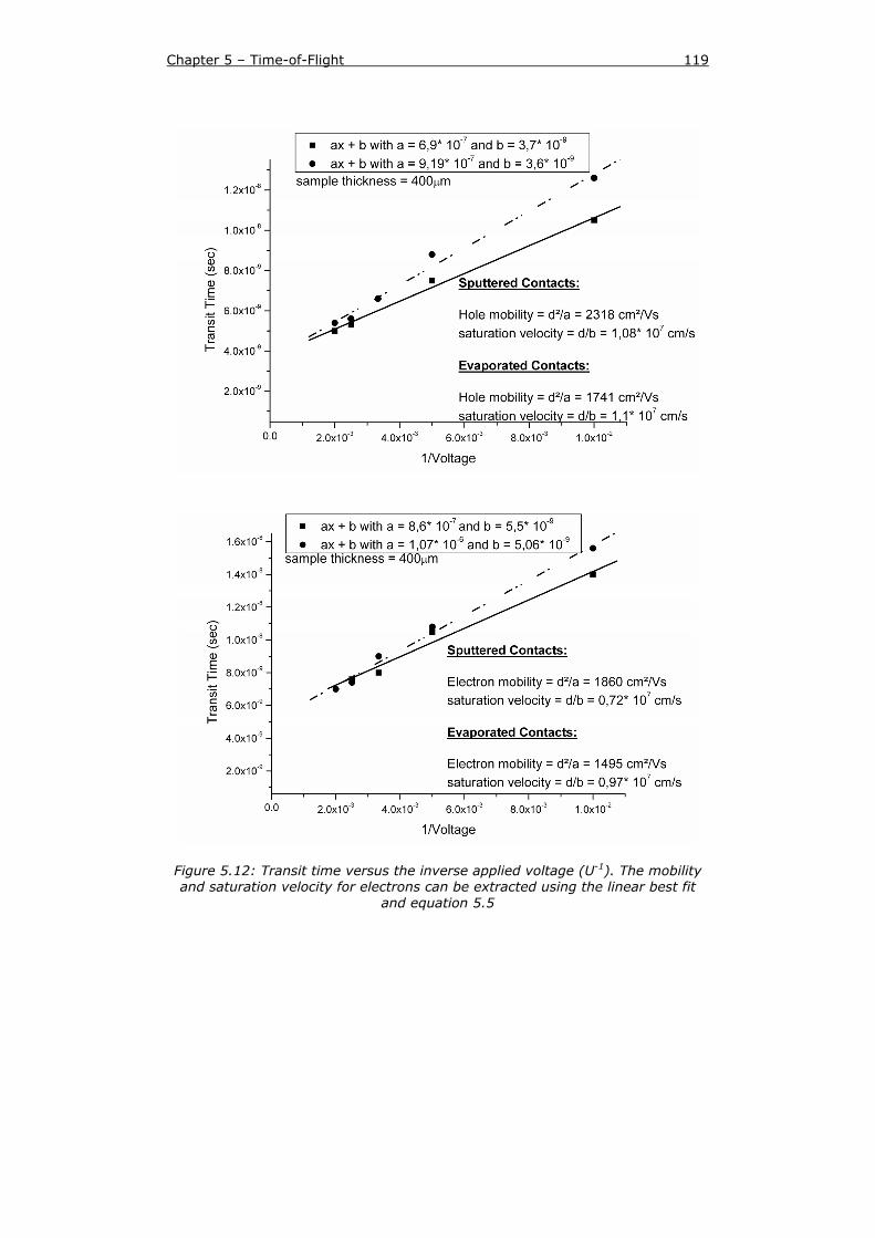
Chapter 5 – Time-of-Flight 119
Figure 5.12: Transit time versus the inverse applied voltage (U-1). The mobility and saturation velocity for electrons can be extracted using the linear best fit
and equation 5.5
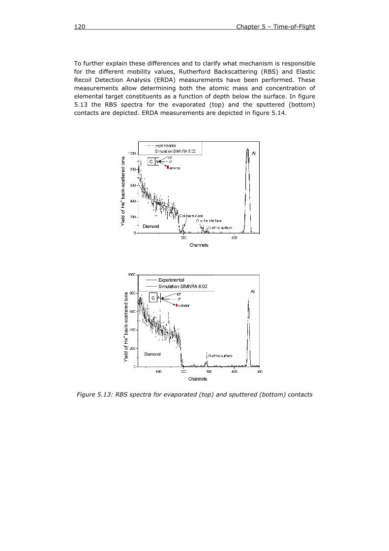
120 Chapter 5 – Time-of-Flight
To further explain these differences and to clarify what mechanism is responsible for the different mobility values, Rutherford Backscattering (RBS) and Elastic Recoil Detection Analysis (ERDA) measurements have been performed. These measurements allow determining both the atomic mass and concentration of elemental target constituents as a function of depth below the surface. In figure 5.13 the RBS spectra for the evaporated (top) and the sputtered (bottom) contacts are depicted. ERDA measurements are depicted in figure 5.14.
Figure 5.13: RBS spectra for evaporated (top) and sputtered (bottom) contacts
Chapter 5 – Time-of-Flight 121
In case of the evaporated contact, a contamination of hydrogen (30 atomic %), carbon (20 atomic %) and oxygen (15 atomic %) at the Al contact surface layer was measured (figure 5.13). Important to notice is the additional presence of 20 atomic % of oxygen in a very thin layer in the contact-diamond interface. In the other case, the sputtered Al contact exhibits a contaminant free Al contact-diamond interface and a comparable surface contamination of oxygen, while the hydrogen surface concentration is more than 2 x lower in this case. The oxygen depth profile at the top of figure 5.13 exhibits two maxima, which are connected with oxygen detected on the surface and in the Al layer. From the bottom part of figure 5.13 it is clear that there is only one maximum connected with oxygen. The sputtered Al contacts exhibit a contaminant free Al contact-diamond interface in the frame of the detection limit of RBS and ERDA analysis, where the lowest detectable amount is about 1015 cm-2 in a background free region of the spectra.
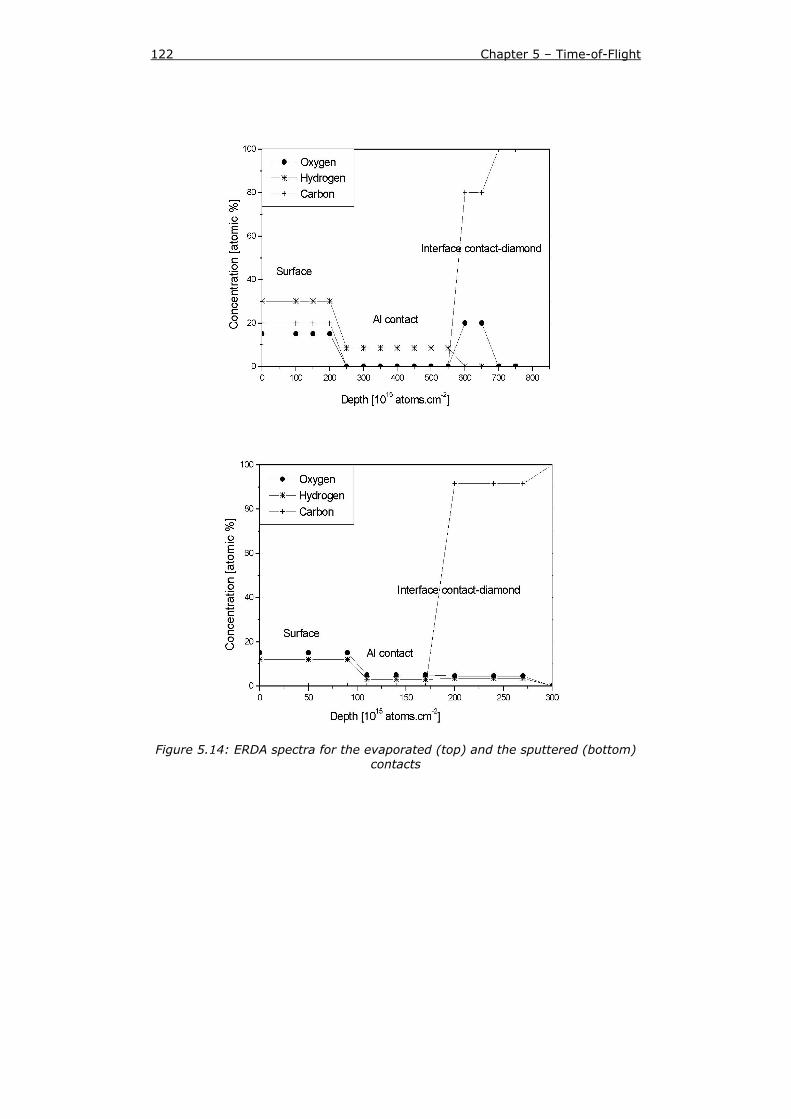
122 Chapter 5 – Time-of-Flight
Figure 5.14: ERDA spectra for the evaporated (top) and the sputtered (bottom) contacts
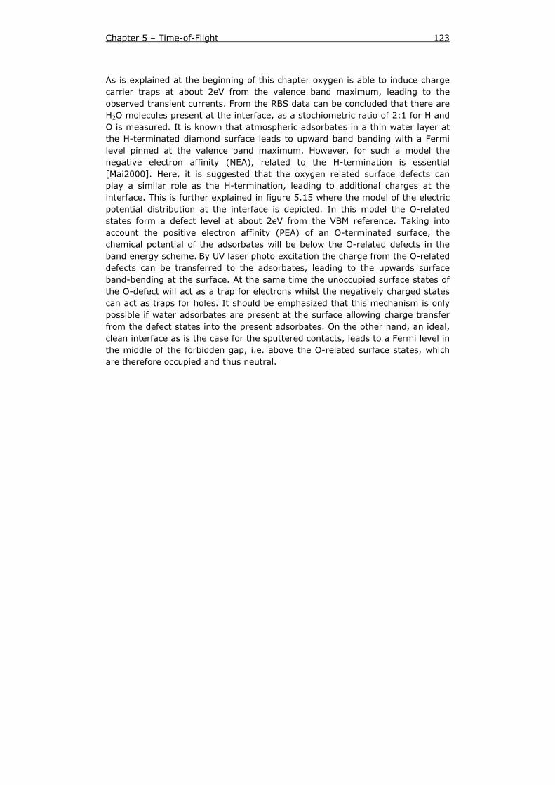
Chapter 5 – Time-of-Flight 123
As is explained at the beginning of this chapter oxygen is able to induce charge carrier traps at about 2eV from the valence band maximum, leading to the observed transient currents. From the RBS data can be concluded that there are H2O molecules present at the interface, as a stochiometric ratio of 2:1 for H and O is measured. It is known that atmospheric adsorbates in a thin water layer at the H-terminated diamond surface leads to upward band banding with a Fermi level pinned at the valence band maximum. However, for such a model the negative electron affinity (NEA), related to the H-termination is essential [Mai2000]. Here, it is suggested that the oxygen related surface defects can play a similar role as the H-termination, leading to additional charges at the interface. This is further explained in figure 5.15 where the model of the electric potential distribution at the interface is depicted. In this model the O-related states form a defect level at about 2eV from the VBM reference. Taking into account the positive electron affinity (PEA) of an O-terminated surface, the chemical potential of the adsorbates will be below the O-related defects in the band energy scheme. By UV laser photo excitation the charge from the O-related defects can be transferred to the adsorbates, leading to the upwards surface band-bending at the surface. At the same time the unoccupied surface states of the O-defect will act as a trap for electrons whilst the negatively charged states can act as traps for holes. It should be emphasized that this mechanism is only possible if water adsorbates are present at the surface allowing charge transfer from the defect states into the present adsorbates. On the other hand, an ideal, clean interface as is the case for the sputtered contacts, leads to a Fermi level in the middle of the forbidden gap, i.e. above the O-related surface states, which are therefore occupied and thus neutral.
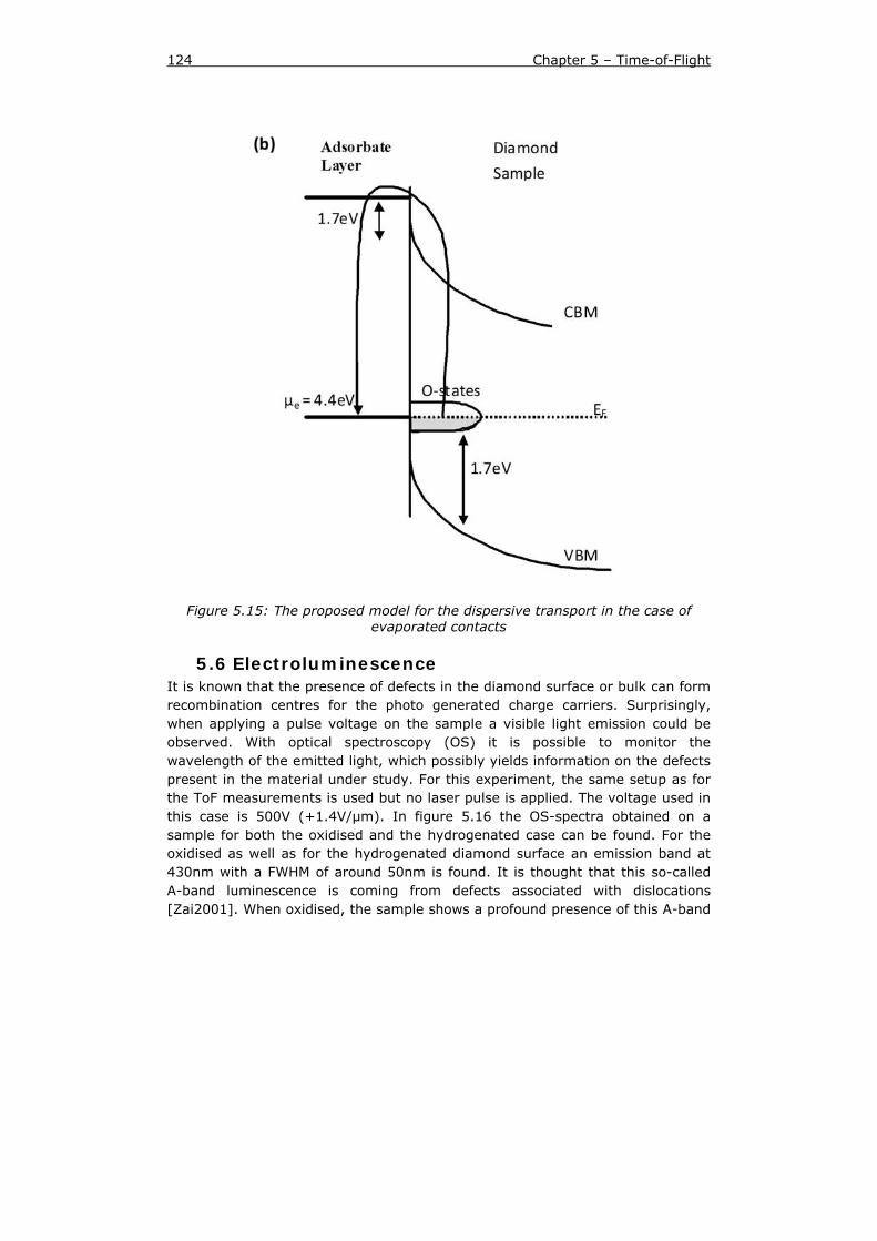
124 Chapter 5 – Time-of-Flight
Figure 5.15: The proposed model for the dispersive transport in the case of evaporated contacts
5.6 Electroluminescence It is known that the presence of defects in the diamond surface or bulk can form recombination centres for the photo generated charge carriers. Surprisingly, when applying a pulse voltage on the sample a visible light emission could be observed. With optical spectroscopy (OS) it is possible to monitor the wavelength of the emitted light, which possibly yields information on the defects present in the material under study. For this experiment, the same setup as for the ToF measurements is used but no laser pulse is applied. The voltage used in this case is 500V (+1.4V/μm). In figure 5.16 the OS-spectra obtained on a sample for both the oxidised and the hydrogenated case can be found. For the oxidised as well as for the hydrogenated diamond surface an emission band at 430nm with a FWHM of around 50nm is found. It is thought that this so-called A-band luminescence is coming from defects associated with dislocations [Zai2001]. When oxidised, the sample shows a profound presence of this A-band
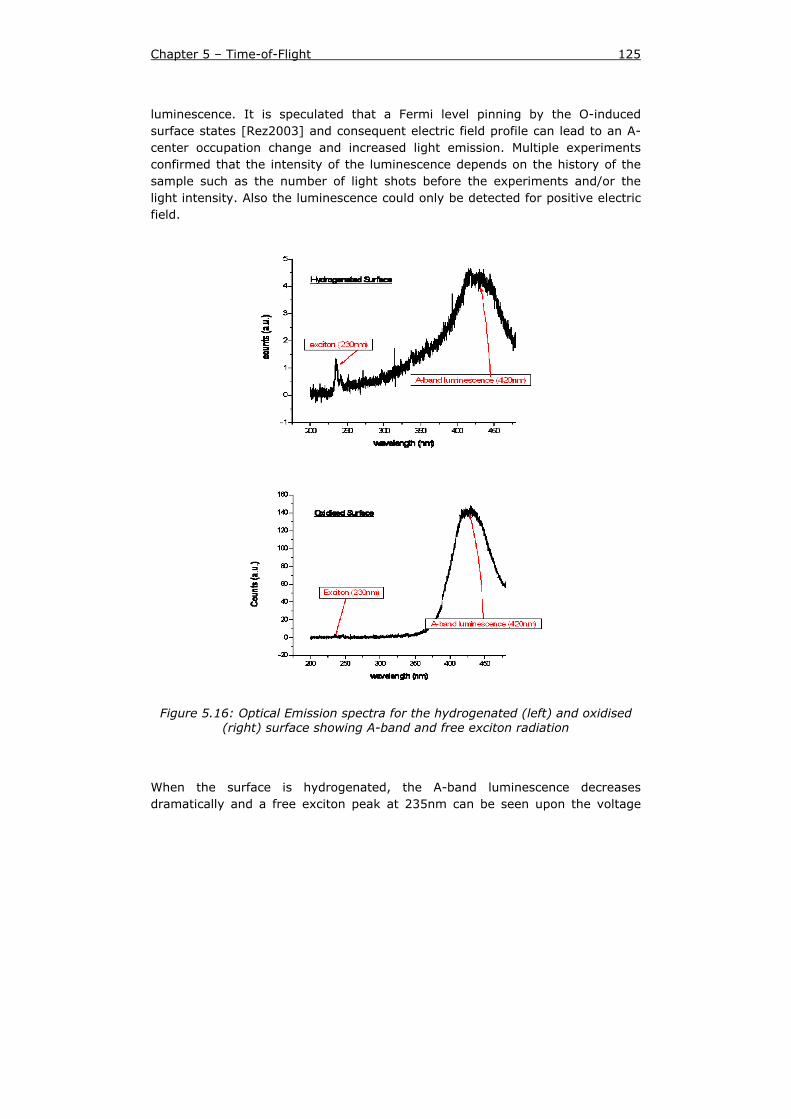
Chapter 5 – Time-of-Flight 125
luminescence. It is speculated that a Fermi level pinning by the O-induced surface states [Rez2003] and consequent electric field profile can lead to an A-center occupation change and increased light emission. Multiple experiments confirmed that the intensity of the luminescence depends on the history of the sample such as the number of light shots before the experiments and/or the light intensity. Also the luminescence could only be detected for positive electric field.
Figure 5.16: Optical Emission spectra for the hydrogenated (left) and oxidised (right) surface showing A-band and free exciton radiation
When the surface is hydrogenated, the A-band luminescence decreases dramatically and a free exciton peak at 235nm can be seen upon the voltage

126 Chapter 5 – Time-of-Flight
pulse. This free exciton peak is coming from exciton recombination [Oku2006]. It suggests that the recombination via A-luminescent channels is reduced upon hydrogenation of the surface, making it more likely for the electron-hole pair to recombine leading to free exciton luminescence. In both cases, the luminescence occurs only at sufficiently high electric fields, causing a carrier injection by tunnelling through the reversely biased Schottky contact. This means that at high electric field our Schottky contacts are leaky. While oxidizing the surface creates defect states at the surface band gap, hydrogenation of the diamond surface creates a fairly better surface with less defect states than for the oxidised surface [Rez2003], leading to less carrier trapping in the surface band gap after the laser photo generation of the electron-hole pairs. These experiments confirm that this luminescence occurs only at high applied electric fields, and only when the polarity of the field was positive with respect to the front contact. In figure 5.17 a picture from the light emission can be seen for the hydrogenated as well as the oxidised surface.
Figure 5.17: Pictures from the light emission from the hydrogenated and oxidised surface
Chapter 5 – Time-of-Flight 127
Bibliography [Bog2007] Bogdan, A., Bogdan, G., De Ceuninck, W., Haenen, K., Nesladek, M., MRS Symp. Proc. 956, 0956-J09-22 (2007)
[Isb2002] Isberg, J., Hammersberg, J., Johansson, E., Wikstrom, T., Twitchen, D.J., Whitehead, A.J., Coe, S.E., Scarsbrook, G.A., Science 297, (2002) 1670
[Isb2004] Isberg, J., Hammersberg, J., Twitchen, D.J., Whitehead, A.J., Diamond and Related Materials 13 (2004) 873
[Mai1991] Main, C., Berkin, J., Bruggemann, R., Marshall, J.M., Journal of Non-Crystalline Solids 137-138 (1991) 442
[Neb1997] Nebel, C.E., Munz, J., Stutzmann, M., Zachai, R. Huttler, H., Physical Review B 55 (1997) 9786
[Nav1980] Nava, F., Canali, C. Ji, C., Reggiani, L., Kozlov, S.F., Solid State Commun. 33, (1980) 475
[Oku2006] Okushi, H., Watanabe, H., Yamasaki, S., Kanno, S., Phys. Stat. Sol. (a) 203 (2006), 3226
[Piv2005] Pivaskas, A., Osterbaka, R., Juska, G., Arlauskas, K., Stubb, H., Synthetic Metals, 155 (2005), 242
[Red1954] Redfield, A.G., Physical Review 94 (1954), 526
[Reg1981] Regianni, L., Bosi, S., Canali, C., Nava, F., Kozlov, S.F., Phys. Rev. B 23, (1981) 3050
[Rez2003] Rezek, B., Sauerer, C., Nebel, C.E., Stutzmann, M., Ristein, J., Ley, L., Snidero, E., Bergonzo, P., Appl. Phys. Lett. 82 (2003), 2266
[Zai2001] Zaitsev, A.M., Optical Properties of Diamond, A Data Handbook, Springer-Verlag, 2001

Wijsheid is de kunst
Per ongeluk de waarheid te zeggen
--- Tim Krabbe, “De Grot” p129 ---
Chapter 6 - Conclusions and Outlook
6.1 Conclusions The main topic of this thesis is to find out about the role of oxygen on (100)-oriented diamond surfaces in the context of the surface electronic structure and the influence on the electrical transport close to the surface. Specifically, the most important property determining the surface electrical properties is the 2DHG conductivity. In the 2DHG conductivity, the role of oxygen is not clear and therefore we tried to deconvolute this important characteristic after studying partially O-terminated (100) diamond surfaces. To achive this goal we have devided this thesis in 3 different parts.
6.1.1 Ultra flat diamond growth In the first part the growth of thin diamond layers has been explored. Based on careful examination of the substrate of the Ib diamond by means of XRD and SEM, the growth procedure has been elucidated. It has been proven that the use of a special designed holder will reduce side effects at the diamond substrate because the density of the hydrogen plasma is homogeneous across the complete surface of the crystal. By SEM it has been shown that changing the growth parameters such as pressure and power will influence the growth mechanism of our diamond layers. By means of the alpha parameter, the possible orientations of growth are examined. When a flat and homogenous layer has finally developed, the surface of the grown (100) layer has been studied with AFM, STM and XRD. It is shown that at the nano-scale the diamond has the 2x1 oriented reconstruction. In the last part of this chapter a big polycrystalline wafer is grown on a silicon substrate with a thickness of more than 1mm. This diamond wafer was made freestanding and cut into smaller diamond samples for surface treatment.
6.1.2 Surface characterization at the nanoscale In the second part of this thesis the surface of our grown, undoped diamond layers has been examined by sensitive surface techniques and terminated with different functional groups. XPS measurements on CVD diamond films, hydrogenated in a H2/O2 plasma (1% of oxygen), show that oxygen is incorporated at the surface of our diamond layer. With a fraction that is clearly a result from the plasma process leading to additional incorporation into the surface as C=O. STS measurements show a wave-like behavior for the second

130 Chapter 6 – Conclusions and Outlook
derivative of the I-V characteristic for the 1% H2/O2-treated diamond layer. This wave-like behavior points to the presence of pinning states in the surface bandgap of the diamond layer due to the presence of oxygen. UPS measurements show that the diamond surface for the 1% H2/O2-treated sample exhibits, just like the well-known fully hydrogenated case, a negative electron affinity (NEA). For this kind of sample the electron affinity is –0.3eV. This demonstrates that although most of the surface of the diamond is covered with hydrogen a small percentage of oxygen quickly reduces the NEA. From these results it can be concluded that oxygen has an influence on the conductivity of the diamond surface. When, after annealing, surface conductivity disappears because of desorption of adsorbates, tunneling is still possible for the 1% H2/O2-treated layer because of the oxygen-related surface states. KPFM (Kelvin Probe Force Microscopy) measurements are performed to check the difference in potential for differently terminated samples. When the diamond surface is hydrogenated it is possible to make the diamond partly oxidised using an AFM tip. On places where the tip is touching the sample, the hydrogenation can be changed to an oxidised and thus resistive surface. This way, new applications such as nano-scale transistors can be made on top of the diamond layer. In a last part of this chapter we have terminated the diamond surface not only with hydrogen and oxygen but also with chlorine. With contact angle measurements the hydrophilic of hydrophobic behavior of these terminations is checked. Further, with IR-SE measurements and XPS it has been proven that a HCl percentage between 15% and 20% in the argon plasma during termination is the most suitable to finish up with a chlorinated surface.
6.1.3 Transport measurements As a last part, Time-of-Flight measurements have been performed on freestanding, undoped diamond layers. These diamond layers are sandwiched between two aluminum contacts and a laser flash is used to create charge carriers at the top contact. ToF measurements have been performed first on oxidised layers and a mobility for holes as big as 2250cm²/Vs and 2050cm²/Vs for electrons has been measured. It is shown that by changing the power of the laser flash ToF measurements can be tuned between 2 different modes, the small signal mode and the space charge limited current mode. In a following approach the surface terminations from the previous chapter are examined. It is shown that for a hydrogenated surface the carrier transport is better than for the oxidised surface. In the case of the oxidised surface defects from O-states at the surface are responsible for trapping of the generated charge carriers. For the hydrogenated surface, less trapping occurs and thus a smoother transport happens. Also temperature dependent measurements, for temperatures in the range of 300 to 600K are performed. It has been proven that the mobility for electrons as well as for holes will go down drastically when the temperature
Chapter 6 – Conclusions and Outlook 131
rises. Acoustic phonon scattering and optical (holes) or intervalley (electrons) phonon scattering mechanism at higher temperatures are the limiting factors for the charge carrier transport. In a last part the influence of contact fabrication on the diamond samples has been studied. It was shown that evaporated contacts on oxidised samples have more incorporation of hydrogen and oxygen in the diamond-contact interface such that O-induced traps appear at the surface creating a dispersive charge transport. The sputtered contacts are created after sputter cleaning such that textbook-like ToF spectra are measured for these contacts. A direct influence of changes of the occupation of O-states by adsorbates is the change of electrical field at the contacts. In the final part the electroluminescence coming from the oxidised surface has been measured with an optical spectroscope. A-band luminescence coming from defects in the diamond is noticed for both surface terminations but a more pronounced exciton emission can be seen for the hydrogenated sample only.
6.2 Outlook As there are three major parts in this thesis also three major areas of interest for future work can be found. In a first stage, the main focus will be put on the deposition conditions and the growth mechanism of thick (100) CVD diamond layers. By carefully mapping all the growth parameters and understanding how experimental parameters such as pressure, power and temperature during growth, influence the physics of the growth, it can be tried to influence and control the main physical characteristics of the diamond layers. Secondary Electron Microscopy (SEM) and Atomic Force Microscopy (AFM) can be used to study the surface of the grown layer and understand better the growth mechanism. Photoelectron Spectroscopy (XPS/UPS), Raman measurements and Time-of-Flight (ToF) studies can give information on the defect incorporation in the bulk of the grown layer. Optical Emission Spectroscopy can be performed to monitor the plasma in-situ such that the influence of different growth species can be studied. Also Scanning Tunneling Microscopy and Spectroscopy (STM/STS) measurements can be measured to confirm results gained by XPS and UPS.
When, by changing all of the important growth parameters, an optimal set of conditions is found, in a second stage the influence of substrate quality and pre-growth plasma treatment on the transport behaviour can be studied by ToF. An O2/H2-plasma will be used to treat the substrate before growth [Tal05, Ach07, Sil08]. It was already shown by the group of Tallaire that high growth rate can be achieved by this pre-growth plasma treatment but the influence on defects was not studied before and can be the focus of this part of the future work. Different concentrations and durations of this plasma treatment can be performed and the quality of the sample after growth, grown with or without pre-treatment can be studied mainly with ToF. Additional characterisation can be
132 Chapter 6 – Conclusions and Outlook
carried out consisting out of photoluminescence (PL), cathodoluminescence (CL) and photocurrent measurements. These measurements will help us to interpret the ToF data according to structural defects induced by the pre-treatment process. This way it should be possible to elucidate the interest of this pre-treatment concerning electron and hole mobilities, and couple this to the possible presence of defects detected with the just mentioned techniques [Neb06].
When the conditions for the growth are set and the pre-treatment is tuned, some 400μm thick diamond layers can be grown. With laser cutting these grown diamond layers can be removed from their substrate followed by a polishing step. The freestanding layers can then be measured with the ToF technique. The mobility measurements for these layers will be compared with the mobility of natural diamond layers and with the theoretically predicted values. Furthermore, temperature dependent ToF measurements will be performed to have a better insight in the transport behaviour of electrons and holes. Even ToF at low temperatures using a cryostat can debate on the limiting factors (phonon scattering) of drift mobilities in diamond. Also ToF can help us to understand the formation of different contacts on the freestanding diamond layer, necessary for electrical applications. Different treatments of the freestanding layer after the growth, such as H-terminated, O-terminated or a mixture between both can be performed to look at the influence of these treatments on the contact formation on our diamond layer. Also different contact preparation techniques such as sputtering or evaporation and the difference between semi-transparent, full contacts or grid structures can be included in this ToF study. Recently the group of Isberg has used a lateral ToF technique where the two contacts are on the same side of the diamond sample, enabling the measurement of transport parallel to the surface. This technique can be used to measure thin layers not removed from the substrate, even allowing to further study the influence of different surface terminations.
Bibliography
[Ach07] J. Achard, F. Silva, O. Brinza, et al. Diamond Relat. Mater. 16 (2007), 685
[Neb06] C.E. Nebel, B. Rezek, D. Shin, H. Watanabe, Phys. Stat. Sol. (a) 203 (2006), 3273
[Sil08] F. Silva, X. Bonnin, J. Achard, et al. Journal of Crystal Growth 310 (2008), 187
[Tal05] A. Tallaire, J. Achard, et al. Phys. Status Solidi, A Appl. Res. 202 (2005), 2059


Appendix 1: List of symbols and abbreviations
α growth parameter
μe Chemical Potential
ρ Density
λ Wavelength
Φ Work function
μ Mobility
τtr Transit Time
τE Extraction Time
ν Frequency
χ Electron Affinity
a Lattice constant
Å Angstrom
2DHG 2-Dimensional Hole Gas
AC Alternating Current
AFM Atomic Force Microscopy
BIOS Biosensor group, IMO
CBM Conduction Band Minimum
CL Cathodoluminescence
CVD Chemical Vapor Deposition
DC Direct Current
DLC Diamond Like Carbon
DNA Deoxyribonucleic acid
DOS Density of States
136 Appendix 1
E Energy
ERDA Elastic Recoil Detection Analysis
ECBM Energy of the conduction band minimum
EB Binding Energy
EF Fermi Level
EG Band gap Energy
EVAC Energy of the vacuum level
EVBM Energy of the valence band maximum
FET field-effect-transistor
FIB Focused Ion Beam
FTIR Fourier Transform Infra-Red Spectroscopy
h Planck’s constant
HPHT High Pressure High Temperature
IMO Institute for Materials Research
IP Ionisation Potential
IR-SE Infra-Red spectroscopic ellipsometry
ISFET ion sensitive field-effect-transistor
KPFM Kelvin Probe Force Microscopy
MOSFET metal-oxide-semiconductor field-effect-transistor
MW PE CVD Microwave Plasma Enhanced Chemical Vapor Deposition
NCD nano-crystalline diamond
NEA Negative Electron Affinity
PEA Positive Electron Affinity
pH Measure of the acidity of a solution
PL Photoluminescence
ppb parts per billion
List of symbols and abbreviations 137
ppm parts per million
Q charge
RBS Rutherford BackScattering
RT Room Temperature
SCLC Space Charge Limited Current
SEM Secondary Electron Microscopy
SHE Standard Hydrogen Electrode (Conditions)
SHG Second Harmonic Generator
STM Scanning Tunneling Microscopy
TBP Tributyl phosphate
THG Third Harmonic Generator
TMB Trimethyl borate
ToF Time-of-Flight
UHV Ultra High Vacuum
UNCD ultra nano-crystalline diamond
UPS Ultraviolet Photoelectron Spectroscopy
UV Ultra Violet
v100 speed of growth in (100) plane
v111 speed of growth in (111) plane
vd Drift Velocity
vsat Saturation Velocity
VBM Valence Band Maximum
VCPD contact potential difference
XPS X-ray Photoelectron Spectroscopy
XRD X-ray Diffraction
Nd:YAG neodymium-doped Yttrium aluminium garnet

Appendix 2: List of figures and tables
Figures
Figure 1.1: The Centenary Diamond is mined in South Africa in 1987 as a rough 500 carat diamond and cut and polished by “The Beers” to produce this optical flawless 300 carat diamond ........................................................................ 5
Figure 1.2: The Phase diagram of carbon where the metastable region for growth of CVD diamond is depicted ............................................................. 7
Figure 1.3: The 3 sp² orbitals and the 4 sp³ orbitals for respectively graphite and diamond formation ............................................................................. 8
Figure 1.4: a) the diamond structure b) the graphite structure [Pre1998] ........ 9
Figure 1.5: The (100) clean surface showing the 2x1 reconstruction, the π-bonded dimmer rows at the surface Left :C(100) 2x1:clean (side view) Right: C(100) 2x1:clean (top view) ................................................................... 11
Figure 1.6: Surface reconstructions for the hydrogenated diamond (100) surface Top: C(100) 2x1:H (side and top view) Bottom: C(100) 1x1:2H (side and top view) .................................................................................................... 12
Figure 1.7: Surface reconstructions for the oxidised diamond (100) surface (side views) Left: C(100) 1x1:O ketone (on-top) Right: C(100) 1x1:O ether (bridge)…. ............................................................................................. 13
Figure 1.8: Surface reconstructions for the (111) diamond surface Left: C(111) 2x1 Right: C(111) 1x1:H ....................................................................... 13
Figure 1.9: Surface reconstructions at the (110) diamond surface Left: C(110) 1x1 Right: C(110) 1x1:H ....................................................................... 14
Figure 1.10: Band bending, electron affinity, work function, Fermi-level, vacuum level, VBM and CBM are introduced ........................................................... 16
Figure 1.11: Conductance measured on two halfs of a (100) diamond showing that adsorbates from the air are needed to induce surface conductivity and that hydrogenation only is not enough [Ris2000] .............................................. 17
Figure 1.12: Due to a difference in electron affinity between C and H a NEA occurs where for the clean and oxidised surface a PEA can be measured [Ris2006] ............................................................................................. 18
Figure 1.13: In the top of this picture, the water layer with adsorbates is depicted on the hydrogenated diamond surface. At the bottom the process of electron transfer up to equilibrium is shown, ending up in an two-dimensional hole gas at the diamond surface ............................................................... 20
140 Appendix 2
Figure 1.14: Measurement of the surface conductivity during the hydrogenation process. Some high sheet conductance can already be seen during the hydrogenation process, without exposure to air [Can2001] .......................... 22
Figure 1.15: Band gaps of several semiconductors as well as for hydrogen-free and hydrogenated diamond. In the inset, the shift in chemical potential can be seen as function of pH ............................................................................ 23
Figure 1.16: Design of a transistor device. Photolithography, e-beam lithography and AFM were combined to fabricate these devices ...................................... 25
Figure 2.1: The 5kW plasma enhanced microwave CVD system (ASTeX PDS17) .. ......................................................................................................... 32
Figure 2.2: The ASTeX 6500 system .......................................................... 33
Figure 2.3: The STS system ..................................................................... 34
Figure 2.4: 3D drawing of the magnetron sputtering system ......................... 35
Figure 2.5: Interaction force as a function of tip-to-sample separation ........... 36
Figure 2.6: The feedback system (PSPD detector) is monitoring the deflection of the cantilever in such a way that a constant normal force is maintained by using the piezoelectric material under the sample ............................................... 37
Figure 2.7: Kelvin Probe Force Microscopy. A conducting cantilever is scanned over a surface at a constant height to map the work function of the surface .... 38
Figure 2.8: Schematic of an STM. Applying a voltage between sample and tip, a tunnelling current will flow. To keep the current or the height above the sample constant a feedback system is used .......................................................... 39
Figure 2.9: Constructive interference for X-ray scattering following Bragg’s law………. ............................................................................................... 41
Figure 2.10: Energy scheme of the XPS process .......................................... 42
Figure 2.11: Hall setup with 2 Tesla magnet and liquid nitrogen cooling .......... 44
Figure 2.12: Contact configuration for the use in Time-Of-Flight measurements. A bias voltage is applied to split the created electrons and holes such that one of them is annihilated at the top contact and the other one drifts to the bottom contact ................................................................................................. 45
Figure 2.13: The Time-Of-Flight setup showing the 3ns laser pulse created from an Nd-YAG laser. The Si-detector used as a trigger for the oscilloscope, the 2 function generators for applying a bias voltage over the sample and triggering of the Q-laser-switch are also shown ............................................................ 46
Figure 2.14: The applied voltage pulse, the laser flash and the measured transit time ..................................................................................................... 47
Figure 2.15: Time-Of-Flight graph showing the 2 different regimes ................ 49
List of figures and tables 141
Figure 2.16: (a) Fitting of transit time to calculate low field mobility and saturation velocity using equation 2.8 (b) Fitting of transit time to calculate low field mobility and saturation velocity using equation 2.10 ............................. 51
Figure 2.17: The forward recoil geometry for ERDA measurements ............... 53
Figure 3.1: The (100)-oriented diamond substrate ..................................... 55
Figure 3.2: Rotating the sample over 180° can give information on the misorientation of the substrate ................................................................ 57
Figure 3.3: The rotation of the diamond sample over an angle of 15 degrees gives different omega values. From the sinusoidal variation found by rotating the sample in steps of 15 degrees the misorientation of the diamond surface can be calculated .............................................................................................. 58
Figure 3.4: {100} and {111} poles of a cubic crystal ................................... 59
Figure 3.5: The pole plots for the {100}, the {110} and the {111} planes showing that the sample is slightly off angle from the (100) orientation .......... 60
Figure 3.6: gas-phase chemistry illustrating the role of CH3 as growth species [May2000] ........................................................................................... 62
Figure 3.7: The Bachmann triangle showing the region where diamond can be grown. It should be noticed that a small addition of methane leads to only a very small region where diamond can be deposited [May2000] ........................... 63
Figure 3.8: A schematic drawing of the deposition system used to grow our thin, atomically flat diamond layers .................................................................. 64
Figure 3.9: The different crystallographic orientations according to the growth parameter α. The arrows are pointing in the direction of fastest growth .......... 65
Figure 3.10: The molybdenum holder to create a smooth connection between substrate and holder ............................................................................... 65
Figure 3.11: AFM images (20 by 20μm) of 4 different layers. (a) CH4/H2-ratio of 0.2% (b) CH4/H2–ratio of 0.4% (c) CH4/H2–ratio of 0.8% (d) CH4/H2–ratio of 1.6% ................................................................................................... 67
Figure 3.12: AFM image of the diamond grown with a CH4/H2-ratio of 1.6%, a power of 500W and a pressure of 105Torr reaching a temperature of 820°C ... 68
Figure 3.13: An AFM image of a very smooth surface on a scale of 20 by 20μm. A roughness of less than 2nm on this scale was achieved ............................. 69
Figure 3.14: X-ray images of the 2θ regions where we expect to see peaks according to crystallographic orientations of the grown diamond .................... 70
Figure 3.15: A topographic image of a diamond surface made by STM. The scanning area is 15 by 15nm .................................................................... 71
Figure 3.16: temperature measurement with a dual wavelength pyrometer for the growth of polycrystalline diamond ....................................................... 72
Figure 3.17: some photographs of the polycrystalline diamond wafer ............. 73
142 Appendix 2
Figure 4.1: The hydrogenation of the diamond surface. Left a fully hydrogenated surface, right a hydrogenation with 1% or 4% of oxygen in the plasma phase is depicted ................................................................................................ 76 Figure 4.2: STM images of the 1% H2/O2 diamond surface (a) without annealing, (b) after UHV annealing for 30min at 200°C and (c) after UHV annealing for 30min at 410°C ...................................................................................... 77
Figure 4.3: The I–V characteristic of the fully hydrogenated surface, showing a quasi-Ohmic character vs. the I–V characteristic of the 1% H2/O2 sample after UHV annealing at 410°C ......................................................................... 79
Figure 4.4: The derivative and second derivative of figure 4.3(b) showing a wave-like behavior pointing to resonances with surface states ..................... 80
Figure 4.5: XPS spectra for the (a) fully hydrogenated surface and (b) for the 1% H2/O2 sample ................................................................................... 81
Figure 4.6: The UPS spectra for the sample hydrogenated in a 1% H2/O2 plasma. The He I spectrum showing a peak corresponding to the NEA of the surface and the He II spectrum to show the fermi level and the work function of this layer……. ............................................................................................... 84
Figure 4.7: A SEM image of the checkerboard pattern as prepared by FIB ....... 85
Figure 4.8: Schematic diagram of the band bending model of the hydrogenated diamond surface in a 1% H2/O2 mixture. The symbols as the electron affinity work function χ, determined by UPS are discussed in the text ....................... 87
Figure 4.9: (a) DOS of the bridging model of the oxidised diamond surface (b) DOS of the on-top model of the oxidised diamond surface ...................... 88
Figure 4.10: (a) Schematics of the setup for local oxidation using an AFM (b) The voltage used to do local oxidation must be at least as big as the 3 parts of the voltage (Vtip , Vwater and Voxide) ........................................................ 90
Figure 4.11: Left is the 2D AFM-image of the diamond surface before oxidation, right is the 2D AFM-image of the surface after oxidation and on the bottom is the 3D AFM-image of the oxidised spot ...................................................... 91
Figure 4.12: A zoom on the oxidised spot from figure 4.11 ........................... 92
Figure 4.13: AFM image of 8 lines written with different speed. The influence on the height and width is obvious ................................................................ 93
Figure 4.14: AFM image of 8 lines written with different tip voltage ................ 93
Figure 4.15: contact angle of a water droplet on a surface ............................ 94
Figure 4.16: Contact angle measurements for the hydrogenated (top-left), oxidised (top-right), chlorinated (bottom-left) and aminated (bottom-right) diamond surface ..................................................................................... 95
List of figures and tables 143
Figure 4.17: Results of IR-SE measurements in the range between 2500 to 3200cm-1. CH2 symmetric (2846 cm-1) and assymmetric (2920 cm-1) stretching vibrations are weaker for samples C and D ................................................. 96
Figure 4.18: The XPS spectrum for the sample chlorinated in a 20% HCl-argon plasma .................................................................................................. 97
Figure 4.19: The amount of Cl at the diamond surface according to the % of HCl in the argon plasma ................................................................................ 98
Figure 5.1: the E6 sample used for Time-of-Flight measurements ................ 102
Figure 5.2: The different steps for contact preparation on oxidised (top) and hydrogenated (bottom) diamond surfaces ................................................ 103
Figure 5.3: the holder for the Time-of-Flight measurements ....................... 104
Figure 5.4: Influence of laser power on the ToF measurements for electrons and holes .................................................................................................. 106
Figure 5.5: ToF spectra for holes (top) and electrons (bottom) for an oxidised sample ................................................................................................ 108
Figure 5.6: Mobility plotted against the electric field for holes (top) and electrons (bottom). The fitting of this curve gives the zero field mobility (μ0) ............. 110
Figure 5.7: ToF spectra for the holes (top) and electrons (bottom) of the hydrogenated diamond sample ............................................................... 111
Figure 5.8: ToF spectrum for the oxidised and hydrogenated diamond surface. The electric field used for these graphs is 1.4 V/µm ................................... 113
Figure 5.9: Hole (top) and electron (bottom) ToF spectra for elevated temperatures at 270°C .......................................................................... 114
Figure 5.10: The temperature dependence of the hole (top) and electron (bottom) mobility for our samples plotted in comparison with the published data……. .............................................................................................. 116
Figure 5.11: Time-Of-Flight spectrum for electrons and holes (inset) obtained from contacts prepared with two different deposition methods: sputtering (---) and thermal evaporation (-o--o-) ............................................................ 118
Figure 5.12: Transit time versus the inverse applied voltage (U-1). The mobility and saturation velocity for electrons can be extracted using the linear best fit and equation 5.5 .................................................................................. 119
Figure 5.13: RBS spectra for evaporated (top) and sputtered (bottom) contacts……. ........................................................................................ 120
Figure 5.14: ERDA spectra for the evaporated (top) and the sputtered (bottom) contacts .............................................................................................. 122
Figure 5.15: The proposed model for the dispersive transport in the case of evaporated contacts ............................................................................. 124
144 Appendix 2
Figure 5.16: Optical Emission spectra for the hydrogenated (left) and oxidised (right) surface showing A-band and free exciton radiation .......................... 125
Figure 5.17: Pictures from the light emission from the hydrogenated and oxidised surface .................................................................................. 126
Tables
Table 1.1: Classification of diamonds according to their nitrogen incorporation……. .................................................................................... 10
Table 1.2: Some properties of diamond as compared to Si and GaN and their related application .................................................................................. 24
Table 4.1: XPS results for samples treated in a 1% H2/O2 plasma and a pure H2 plasma. A chemically oxidised sample is given as a reference........................ 82
Table 5.1: The corresponding data for the ToF measurements for holes (top) and electrons (bottom) from figure 5.5 .......................................................... 109
Appendix 3: List of publications and presentations
Publications
2009 Contact properties of CVD diamond as studied by Time-of-Flight W. Deferme, A. Mackova, K. Haenen, M. Nesládek
Appl. Phys. Lett. (ter publicatie aangeboden) 2008 The influence of different surface terminations on electrical transport and emission properties for freestanding single crystalline (100) CVD diamond samples W. Deferme, A. Bogdan, K. Haenen, W. De Ceuninck, C.F.J. Flipse, M. Nesládek, MRS Symposium Proceedings Volume 1039 (2008), 1039-P15-30, 83-89. In “Diamond Electronics – Fundamentals to Applications II”, Eds. C.E. Nebel, R.B. Jackman, R.J. Nemanich, M. Nesládek, ISBN 978-1-55899-986-2 Charge transport in high mobility single crystal diamond M. Nesladek, A. Bogdan, W. Deferme, N. Tranchant, P. Bergonzo Diamond and Related Materials 17: 1235–1240 (2008) 2007 Transport measurements and emission properties of freestanding single crystalline CVD diamond samples W. Deferme, A. Bogdan, K. Haenen, W. De Ceuninck, M. Nesladek, Electrical physica status solidi (a) 204: 3017-3022 (2007) Titanium nitride growth by sputtering for contacts on boron doped diamond V. Mortet, O. Elmazria, W. Deferme, M. Daenen, J. D'Haen, A. Lazea, A. Morel, K. Haenen, M. D'Olieslaeger, Plasma Processes and Polymers 4/S1 (2007), S139-S143. Electrostatic force microscopy of electrical conductivity of hydrogen-terminated CVD diamond films A. Volodin, C. Toma, G. Bogdan, W. Deferme, K. Haenen, M. Nesladek, C. Van Haesendonck physica status solidi (a) 204: 2915-2919 (2007)
146 Appendix 3
Voltage dependent modification of hydrogen-terminated diamond surface using a conductive atomic force microscope tip C. Toma, A. Volodin, G. Bogdan, W. Deferme, K. Haenen, M. Nesladek, C. Van Haesendonck Physica status solidi (a) 204: 2920-2924 (2007) Electrostatic force microscopy mapping of electrical conductivity of hydrogen-terminated diamond films A.Volodin, C. Toma, G. Bogdan, W. Deferme, K. Haenen, M. Nesladek, C. Van Haesendonck Appl. Phys. Lett.91, 142111 (2007) 2006 Compositional and electrical characterisation of the hydrogen-oxygen terminated diamond (100) surface W. Deferme, K. Haenen, G. Tanasa, C. F. J. Flipse, M. Nesládek Physica Status Solidi (a) 203: 3114-3120 (2006) The role of (sub)-surface oxygen on the surface electronic structure of hydrogen terminated (100) CVD diamond W. Deferme, G. Tanasa, J. Amir, K. Haenen, M. Nesladek, C.F.J. Flipse Diamond and Related Materials 15: 687-691 (2006) Investigation of hydrogenated CVD diamond films by photo-thermal ionization spectroscopy A. Hikavyy, P. Clauws, W. Deferme, G. Bogdan, K. Haenen, M. Nesladek, Diamond and Related Materials 15: 682-686 (2006) Thick single crystal CVD diamond prepared from CH4-rich mixtures G. Bogdan, K. De Corte, W. Deferme, K. Haenen, M. Nesládek Physica Status Solidi (a) 203: 3063-3069 (2006) 2005 Head-on immobilization of DNA fragments on CVD-diamond layers S. Wenmackers, P. Christiaens, W. Deferme, M. Daenen, K. Haenen, M. Nesladek, P. Wagner, V. Vermeeren, L. Michiels, M. vandeVen, M. Ameloot, J. Wouters, L. Naelaerts and Z. Mekhalif Materials Science Forum 492-493: 267-272 (2005) PTIS investigation of hydrogenated CVD diamond films A. Hikavyy, P. Clauws, W. Deferme, G. Bogdan, K. Haenen, M. Nesladek physica status solidi (a) 202: 2171-2176 (2005)
List of articles and presentations 147
Oral Presentations 2009 W. Deferme, A. Mackova, K. Haenen, M. Nesládek
“Contact properties of CVD diamond as studied by Time-of-Flight”, Congres Hasselt Diamond workshop 2009, SBDD XIV, 2 – 4 maart 2009, Cultuurcentrum Hasselt, Hasselt, België. 2008 W. Deferme, A. Bogdan, K. Haenen, W. De Ceuninck, M. Nesladek “Temperature dependent TOF measurements on undoped (100) diamond layers”, Achtste “Diamond Day” (follow-up meeting SBO-project), 30 April 2008, UHasselt (Diepenbeek) 2007 M. Nesladek, N. Tranchant, H. Hamrita, D. Tromson, C. Mer, P. Bergonzo, A. Bogdan, A. Bogdan, W. Deferme, M. Pomorski “Charge Transport in High Mobility CVD Diamond”, 18th European Conference on Diamond, Diamond-like Materials, Carbon nanotubes and Nitrides, September 9-14, 2007, Berlin, Germany, 2007 2006 G. Bogdan, W. Deferme, J. Cervenka, C.F.J. Flipse, B. Willems, G. Van Tendeloo, K. Haenen, M. Nesládek, “The growth mechanism of near-atomically flat single crystal (100) CVD diamond in CH4-rich gas precursors”, 17th European Conference on Diamond, Diamond-like Materials, Carbon Nanotubes, and Nitrides, Estoril Congress Centre, Estoril, Portugal, September 3-8, 2006 2005 W. Deferme, G. Tanasa, J. Amir, K. Haenen, M. Nesládek, C.F.J. Flipse “The role of (sub)-surface oxygen on the surface electronic structure of hydrogen terminated (100) CVD diamond”, 16th European Conference on Diamond, Diamond-Like Materials, Carbon Nanotubes and Nitrides 11-16 September 2005, Toulouse, France W. Deferme, V. Mortet, K. Haenen, M. Nesladek B-doping on (100)-diamond, Derde “Diamond Day” (follow-up meeting SBO-project), 13 April 2005, UHasselt (Diepenbeek)

148 Appendix 3
A. Hikavyy, P. Clauws, W. Deferme, G. Bogdan, K. Haenen, M. Nesládek, “PTIS investigation of hydrogenated CVD diamond films”, Surface and bulk defects in CVD diamond films, X, Limburgs Universitair Centrum, Diepenbeek, Belgium, February 23-25, 2005 2004 W. Deferme, M. Nesladek, S. Wenmackers, G. Tanasa, C.F.J.Flipse “The hydrogenation of the diamond surface examined by XPS and STM in UHV”, Belgian Physical Society (BPS) – International Meeting, 25-26 Mei 2004, Bergen S. Wenmackers, P. Christiaens, W. Deferme, K. Haenen, M. Nesládek, P. Wagner, L. Michiels, M. vandeVen, V. Vermeeren, M. Ameloot, J. Wouters, Z. Mekhalif, “Surface sensitive techniques for the study of DNA immobilized on CVD diamond”, Multifunctional and Functionally Graded Materials, Aula Pieter De Somer, Katholieke Universiteit Leuven, Leuven, Belgium, July 11-14, 2004
Poster Presentations 2008 Best Student Poster Prize W. Deferme, W. De Ceuninck, K. Haenen, M. Nesládek, “Temperature Dependent I-V and TOF measurements on undoped (100) diamond layers”, 19th European Conference on Diamond, Diamond-like Materials, Carbon Nanotubes, and Nitrides, Meliá Sitges Hotel, Sitges, Spain, September 7-11, (2008) W. Deferme, W. De Ceuninck, K. Haenen, M. Nesládek, “Time-Of-Flight study of freestanding single crystalline (100) CVD diamond samples in function of surface termination and temperature”, 2nd International Conference on New Diamond and Nano Carbons (NDNC2008), Grand Hotel, Taipei, Taiwan, May 26-29, (2008) W. Deferme, G. Bogdan, K. Haenen, W. De Ceuninck, C.F.J. Flipse, M. Nesládek, “Effect of the surface termination on the low field electrical mobility in the Time of Flight experiments”, Hasselt Diamond Workshop 2008 – SBDD XIII, cultuurcentrum Hasselt, Hasselt, Belgium, February 25-27, (2008)
List of articles and presentations 149
2007 W. Deferme, A. Bogdan, K. Haenen, W. De Ceuninck, C.F.J. Flipse, M. Nesládek, “The influence of different surface terminations on electrical transport and emission properties for freestanding single crystalline (100) CVD diamond samples”, MRS 2007 Fall Meeting, Hynes Convention Center & Sheraton Boston Hotel, Boston, MA, USA, November 26-30, (2007) V. Mortet, M. Daenen, T. Teraji, A. Lazea, J. D’Haen, W. Deferme, K. Haenen, M. D'Olieslaeger, “Characterization of boron doped diamond epilayers growth in a NIRIM type reactor”, 18th European Conference on Diamond, Diamond-like Materials, Carbon Nanotubes, and Nitrides, Maritim Hotel Berlin, Berlin, Germany, September 9-14, (2007) C. Toma, A. Volodin, G. Bogdan, W. Deferme, K. Haenen, M. Nesládek, C. Van Haesendonck, “Voltage dependent modification of hydrogen-terminated diamond surface using a conductive atomic force microscope tip”, Hasselt Diamond Workshop – SBDD XII, Hasselt University, Diepenbeek, Belgium, February 28-March 2, (2007) A. Volodin, C. Toma, G. Bogdan, W. Deferme, K. Haenen, M. Nesládek, C. Van Haesendonck, “Electrostatic force microscopy of electrical conductivity of hydrogen-terminated CVD diamond films”, Hasselt Diamond Workshop – SBDD XII, Hasselt University, Diepenbeek, Belgium, February 28-March 2, (2007) W. Deferme, A. Bogdan, K. Haenen, W. De Ceuninck, M. Nesládek, “Electrical transport measurements and emission properties of freestanding single crystalline CVD diamond samples”, Hasselt Diamond Workshop – SBDD XII, Hasselt University, Diepenbeek, Belgium, February 28-March 2, (2007) G. Bogdan, O. Douhéret, W. Deferme, K. De Corte, P. Geithner, J. Ristein, B. Cann, M.E. Newton, K. Haenen, M. Nesládek, “Spectroscopic characterisation of single crystal CVD diamond”, Hasselt Diamond Workshop – SBDD XII, Hasselt University, Diepenbeek, Belgium, February 28-March 2, (2007)
150 Appendix 3
2006 V. Mortet, O. Elmazria, W. Deferme, M. Daenen, J. D'Haen, A. Morel, K. Haenen, M. D'Olieslaeger, “Titanium nitride growth by sputtering for contacts on boron doped diamond”, Tenth International Conference on Plasma Surface Engineering (PSE 2006), Kongresshaus, Garmisch-Partenkirchen, Germany, September 10-15, (2006) W. Deferme, C.F.J. Flipse, G. Tanasa , K. Haenen, M. Nesládek, “The role of (sub)-surface oxygen on the surface electronic structure of hydrogen terminated (100) CVD diamond”, Fysica 2006, Leiden University, Leiden, The Netherlands, April 28, (2006)
G. Bogdan, W. Deferme, K. De Corte, K. Haenen, M. Nesládek, “Growth and characterization of single crystal CVD diamond prepared from CH4-rich mixtures”, Fysica 2006, Leiden University, Leiden, The Netherlands, April 28, (2006)
A. Hikavyy, P. Clauws, G. Bogdan, W. Deferme, K. Haenen, M. Nesládek, “PTIS investigation of undoped hydrogenated CVD diamond films”, Materials Congress 2006, Carlton House Terrace, London, UK, April 5-7, (2006)
W. Deferme, M. Daenen, O. Douhéret, C.F.J. Flipse, G. Tanasa, K. Haenen, M. Nesládek, “Mobility and electron affinity of differently hydrogen-oxygen terminated (100) CVD diamond”, Surface and bulk defects in CVD diamond films, XI, Hasselt University, Diepenbeek, Belgium, February 22-24, (2006)
2005 A. Hikavyy, P. Clauws, W. Deferme, G. Bogdan, M. Nesládek, K Haenen, “Investigation of hydrogenated CVD diamond films by photo-thermal ionization spectroscopy”, 16th European Conference on Diamond, Diamond-like Materials, Carbon Nanotubes, and Nitrides, Centre de Congrès Pierre Baudis, Toulouse, France, September 11-16, (2005)
P. Christiaens, S. Wenmackers, W. Deferme, M. Daenen, O. Williams, K. Haenen, V. Vermeeren, L. Michiels, M. vandeVen, P. Wagner, “pH-dependent surface conductivity of synthetic diamond films”, Congrès Général - Société Française de Physique et Belgian Physical Society, Université de Lille, Lille, France, 29.08-02.09.05 (2005)
P. Christiaens, S. Wenmackers, W. Deferme, M. Daenen, O. Williams, K. Haenen, V. Vermeeren, L. Michiels, M. vandeVen, P. Wagner, “pH-sensitive polycrystalline diamond (PCD) films”, 3rd International Symposium on Sensor Science (I3S 2005), Jülich, Germany, July 18-21, (2005)
List of articles and presentations 151
2004 W. Deferme, M. Nesládek, S. Wenmackers, V. Mortet, K. Haenen, G. Tanasa, C.F.J. Flipse, Z. Mekhalif, M. Cannaerts, D. Buntinx, C. Van Haesendonck, “The 2DHG on hydrogenated CVD diamond surfaces: a growth and characterisation study”, Meeting of the Accompanying Committee IAP V/01, Facultés Universitaires Notre-Dame de la Paix, Namur, Belgium, November 8, (2004)
S. Wenmackers, P. Christiaens, W. Deferme, G. Vanhoyland, K. Haenen, M. Nesládek, P. Wagner, V. Vermeeren, L. Michiels, M. vandeVen, M. Ameloot, J. Wouters, Z. Mekhalif, “Surface sensitive techniques for the study of biologically activated CVD diamond”, International Scientific Meeting, Belgian Physical Society, Université de Mons-Hainaut, Mons, Belgium, May 25-26, (2004)
S. Wenmackers, P. Christiaens, W. Deferme, G. Vanhoyland, K. Haenen, M. Nesládek, P. Wagner, V. Vermeeren, L. Michiels, M. vandeVen, M. Ameloot, J. Wouters, Z. Mekhalif, “Surface sensitive techniques for the study of biologically activated CVD diamond”, Cells at work, Life Sciences Limburg, University Maastricht, Maastricht, The Netherlands, May 13, (2004)
S. Wenmackers, P. Christiaens, W. Deferme, K. Haenen, M. Nesládek, P. Wagner, L. Michiels, M. vandeVen, V. Vermeeren, M. Ameloot, J. Wouters, Z. Mekhalif, “Surface sensitive techniques for the study of DNA immobilized on CVD diamond”, Nanostructures and self-assembled monolayers, IAP WP7-symposium, Facultés Universitaires Notre-Dame de la Paix, Namur, Belgium, February 19-20, (2004)