Embed Size (px)
Citation preview
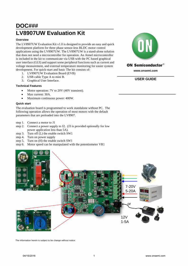
DOC### LV8907UW Evaluation Kit Overview The LV8907UW Evaluation Kit v1.0 is designed to provide an easy and quick development platform for three phase sensor-less BLDC motor control applications using the LV8907UW. The LV8907UW is a stand-alone solution that does not need a microcontroller for operation. An Atmel microcontroller is included in the kit to communicate via USB with the PC based graphical user interface (GUI) and support some peripheral functions such as current and voltage measurement, and external temperature monitoring for easier system development. For quick-start and basic The kit consists of:
1. LV8907UW Evaluation Board (EVB) 2. USB cable Type A to mini B. 3. Graphical User Interface.
Technical Features • Motor operation: 7V to 20V (40V transient). • Max current: 30A. • Maximum continuous power: 400W.
Quick start The evaluation board is programmed to work standalone without PC. The following operation allows the operation of most motors with the default parameters that are preloaded into the LV8907. step 1. Connect a motor to J1 step 2. Connect a power supply to J2. (J3 is provided optionally for low
power application less than 5A). step 3. Turn off (L) the enable switch SW1 step 4. Turn on power supply step 5. Turn on (H) the enable switch SW1 step 6. Motor speed can be manipulated with the potentiometer VR1
www.onsemi.com
USER GUIDE
The information herein is subject to be change without notice.
7-20V5-20A
12V1-5A
or
04/15/2016 1 www.onsemi.com
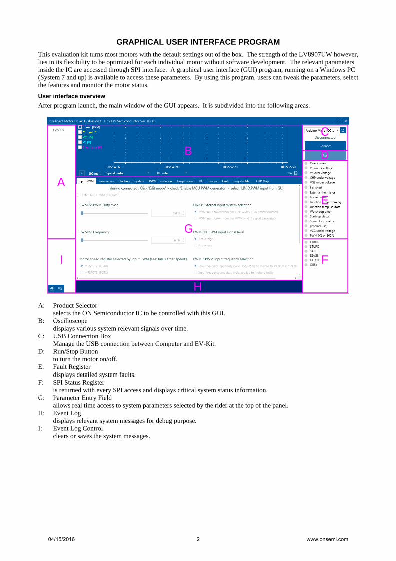
GRAPHICAL USER INTERFACE PROGRAM This evaluation kit turns most motors with the default settings out of the box. The strength of the LV8907UW however, lies in its flexibility to be optimized for each individual motor without software development. The relevant parameters inside the IC are accessed through SPI interface. A graphical user interface (GUI) program, running on a Windows PC (System 7 and up) is available to access these parameters. By using this program, users can tweak the parameters, select the features and monitor the motor status.
User interface overview After program launch, the main window of the GUI appears. It is subdivided into the following areas.
A: Product Selector
selects the ON Semiconductor IC to be controlled with this GUI. B: Oscilloscope
displays various system relevant signals over time. C: USB Connection Box
Manage the USB connection between Computer and EV-Kit. D: Run/Stop Button
to turn the motor on/off. E: Fault Register
displays detailed system faults. F: SPI Status Register
is returned with every SPI access and displays critical system status information. G: Parameter Entry Field
allows real time access to system parameters selected by the rider at the top of the panel. H: Event Log
displays relevant system messages for debug purpose. I: Event Log Control
clears or saves the system messages.
A
CB D
E
G
H
I F
04/15/2016 2 www.onsemi.com
GUI Installation Program installation is required for first time use. The installation is described in “Device Driver and Program Installation” on page 9. Administrator rights are necessary.
Basic GUI Operation These basic instructions explain how to:
1. Setup the board 2. Start the GUI 3. Link the board 4. Run a motor 5. Motor control with GUI 6. Oscilloscope 7. Fault Messages
Setup the board A motor and power supply should be connected as described on page 1 and the USB cable must be connected. The enable switch SW1 must be turned to L to allow control by the GUI program. If it is the first time to connect the board by USB, the device driver installation is required. See “Device Driver and Program Installation” on page 9.
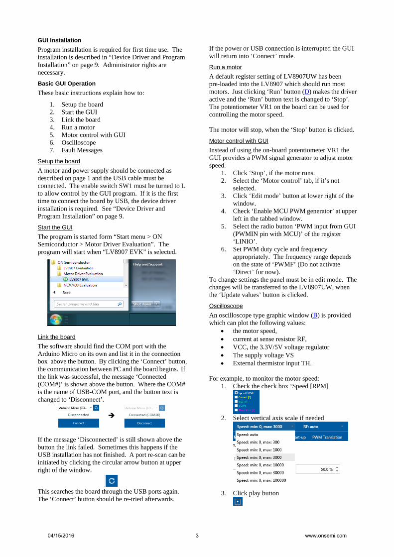
Start the GUI The program is started form “Start menu > ON Semiconductor > Motor Driver Evaluation”. The program will start when “LV8907 EVK” is selected.
Link the board The software should find the COM port with the Arduino Micro on its own and list it in the connection box above the button. By clicking the ‘Connect’ button, the communication between PC and the board begins. If the link was successful, the message ‘Connected (COM#)’ is shown above the button. Where the COM# is the name of USB-COM port, and the button text is changed to ‘Disconnect’.
If the message ‘Disconnected’ is still shown above the button the link failed. Sometimes this happens if the USB installation has not finished. A port re-scan can be initiated by clicking the circular arrow button at upper right of the window.
This searches the board through the USB ports again. The ‘Connect’ button should be re-tried afterwards.
If the power or USB connection is interrupted the GUI will return into ‘Connect’ mode.
Run a motor A default register setting of LV8907UW has been pre-loaded into the LV8907 which should run most motors. Just clicking ‘Run’ button (D) makes the driver active and the ‘Run’ button text is changed to ‘Stop’. The potentiometer VR1 on the board can be used for controlling the motor speed. The motor will stop, when the ‘Stop’ button is clicked.
Motor control with GUI Instead of using the on-board potentiometer VR1 the GUI provides a PWM signal generator to adjust motor speed.
1. Click ‘Stop’, if the motor runs. 2. Select the ‘Motor control’ tab, if it’s not
selected. 3. Click ‘Edit mode’ button at lower right of the
window. 4. Check ‘Enable MCU PWM generator’ at upper
left in the tabbed window. 5. Select the radio button ‘PWM input from GUI
(PWMIN pin with MCU)’ of the register ‘LINIO’.
6. Set PWM duty cycle and frequency appropriately. The frequency range depends on the state of ‘PWMF’ (Do not activate ‘Direct’ for now).
To change settings the panel must be in edit mode. The changes will be transferred to the LV8907UW, when the ‘Update values’ button is clicked.
Oscilloscope An oscilloscope type graphic window (B) is provided which can plot the following values:
• the motor speed, • current at sense resistor RF, • VCC, the 3.3V/5V voltage regulator • The supply voltage VS • External thermistor input TH.
For example, to monitor the motor speed:
1. Check the check box ‘Speed [RPM]
2. Select vertical axis scale if needed
3. Click play button
04/15/2016 3 www.onsemi.com

4. Click ‘Run’ button Be aware, that the displayed speed will be in “electrical revolutions” per minute (i.e. for a two pole motor). To display physical motor speed it is necessary to enter the number of poles in the ‘Parameters’ window described in the next section and clear the plot to display the new scale by selecting stop and play from the graph window. The oscilloscope also includes a recoding function. The CSV button exports data in a .CSV (comma separated values) format file.
The file can be read with Microsoft Excel. The maximum data length is 5000. The sampling interval can be changed by the up-down menu next to the play button. All data traces are exported into the .CSV file, even if they are not displayed. A screen copy function is also provided. It supports JPEG, JPEG FIF and PNG. Its button is located next to the CSV button.
Fault Messages While connected, the GUI will display real time system fault messages in the Fault Register (E). Following is a list of the faults and possible remedies: • Over current:
The maximum system current was exceeded (200mV across the shunt resistor). Since the LV8907UW has cycle by cycle current limit, an overcurrent error can either be caused by a fast transient. If persistent this indicates a serious problem such as a short across the power stage, or a loose connection in the board routing. It is recommended to return the EV-Kit.
• VS under voltage: The supply voltage has fallen below 7V. Probably because the power supply is too soft.
• VS over voltage: The supply voltage has risen above 21V. Maybe because the motor dumped charge into the system after being disabled.
• CHP under voltage: The high-side charge pump capacitor on CHP has lost charge or is malfunctioning, or one of the charge pump caps is faulty.
• VGL under voltage: The low-side charge pump capacitor has lost charge or is malfunctioning, or one of the charge pump caps is faulty.
• FET short The voltage drop across one of the inverter FETs has exceeded its programmed maximum value. Probably a system parameter error, increase FSCDL.
• External Thermistor The voltage at pin TH as fallen below the programmed threshold. Adjust the threshold
parameter THTH or make sure pin TH has been tied to V3RO and not GND to disable it.
• Locked Rotor The motor has gone through “open loop startup” but is not providing a back EMF after the startup timer has run out. Usually this lights up with ‘Start-up Status’. Either there is no motor connected, or the startup parameters are wrong. It may also be that the shunt resistor is too large for this motor, so the current limit prevents a large motor from turning.
• Junction temp. warning The IC temperature has exceeded the warning threshold (125°C or 150°C) depending on TSTS.
• Junction temp. shutoff The IC temperature has exceeded the shutoff level threshold (150°C or 175°C) depending on TSTS.
• Watchdog timer has run out without being triggered. This error will always be displayed if the watchdog register is not being written to within the window. It is usually disabled and has no effect, if enabled in register WDTEN, the LV8907 will respond to the error.
• Start-up Status The LV8907UW is in open loop startup mode. The error goes away once a back EMF has been reliably detected.
• Speed loop status error is flagged if the speed control algorithm within the LV8907UW is enabled and the measured speed is more than 6.25% different from the target speed.
• VCC under voltage The VCC (3.3V/5V) regulator is below its minimum threshold. Probably overloaded.
• PWM 0% or 100% error indicates that input PWM is not switching, probably static low or high.
04/15/2016 4 www.onsemi.com
Advanced GUI Operation and System Setup The LV8907UW parameters and some motor related functions are categorized into the following riders at the top of Parameter Entry Field (G).
- Input PWM - Program Parameters - Start-up parameters - Fundamental System configurations - Command PWM Translation - Target speed setting for the closed loop
control - PI parameter of the closed loop speed control - Inverter control parameters - Fault handling setting - Bit/byte base Registers Map - OTP memory Map
The each serial port register is titled by its name specified in the data sheet with a brief description. For some of multiple bit registers, the three-way input method is provided. It can be set with a slide bar, physical value or direct code. The tabbed windows have ‘Edit mode’ button to change the values and settings. And, once the ‘Update values’ button is clicked, the registers will be updated. It prevents that intermediate values are immediately updated back-and-forward, while the nob of the slide bar is dragged.
In the LV8907UW, there are registers which can be written during the standby mode only. The buttons of such registers are automatically gray-out during the run mode.
Input PWM In this window, a PWM signal generated by the on-bard MCU is controlled. This signal is connected to the PWMIN pin of the LV8907UW. The PWM signal of the on-board potentiometer is connected to the LINPWMIN pin. The input is switched by LINIO bit. The GUI controlled MCU PWM is selected, when the radio button ‘PWM input from GUI (PWMIN pin with MCU)’ is selected.
Parameters The number of poles and the resistance of current sense resistor RF are specified in this window. They are used in the GUI program for the conversion of the rotational speed and the current individually. It is highly recommended to set these parameters at the beginning. When these are changed intermediate of the operation, the following manual operations are required.
- Refresh the oscilloscope plots by toggle Stop/Play button when it is playing.
- Refresh the RPM text boxes of the register FGTs in the tabbed window ‘Target speed’ by clicking ‘Edit mode’ and ‘Cancel’ consecutively.
The ‘Communication timeout’ is not related to the motor nor motor driver. It is used for the USB
communication with the board. Users don’t have to consider it, usually.
Register Map The parameter settings modified in other tabbed windows except OTP Map, are applied to the LV8907UW registers. In this window, the register map is shown, reading back from LV8907UW registers. Where the cell color
- green represents 1 - white represents 0 - dark red represents 1 of a read-only register - pink represents 0 of a read-only register
Whenever the bit cell is clicked, 1 and 0 is toggled. Clicking over the register address or name cell, the byte based modification is activated. For use of next time, or for copy to OTP, the register map can be saved to a CSV file with ‘Export’ button. Optionally, you can add a short note in to the first line of the CSV file with the ‘Export comment’ text box before saving the file.
And, the ‘Import’ button loads the register map values from a CSV file to the LV8907UW registers directly.
OTP Map The LV8907UW has a non-volatile memory for the standalone operation in the user application. The memory is a one-time programing (OTP) type. The board of this EV-kit is not designed to allow users to write OTP. The tools, which are compatible to this GUI program, for OTP memory writing are provided. Please contact to local ON Semiconductor sales office for the technical support. The OTP writing procedure:
1. Load a register map from the file which is saved in the Register Map window by Import button. At this step, the map data are stored in the PC memory.
2. Manual touch up can be done by clicking the bit cells if needed.
3. To write OTP memory, the following conditions must be met.
a. Communication line to the board is successfully connected through a USB.
b. The power supply voltage is higher than 14V.
c. EN pin low (motor stop) 4. Click ‘Write’ button
The following optional functions are provided as well. - Read OTP and show in the map cells - Save the OTP map stored in the PC memory to
the file.
04/15/2016 5 www.onsemi.com
HARDWARE DESCRIPTION
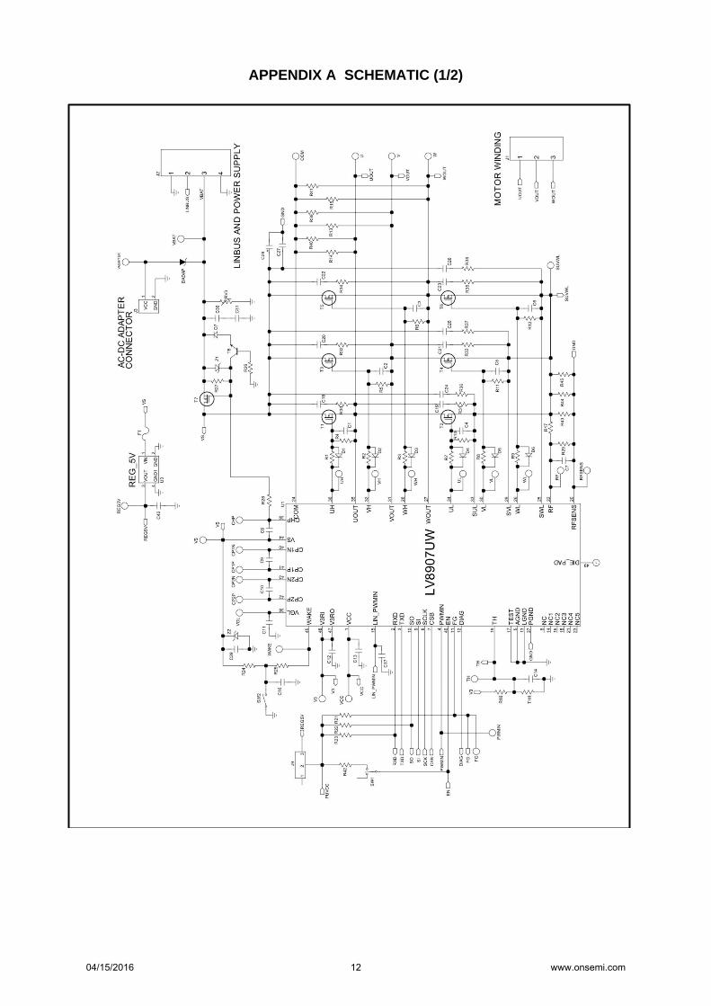
Detailed Description The LV8907 is the central controller on the EVB that implements the sensor-less commutation algorithm, provides user-selectable system control functions and drives the motor through the on-board N-MOSFET based inverter. Refer Appendix A Schematic (1/2) on page 12 and followng pages.
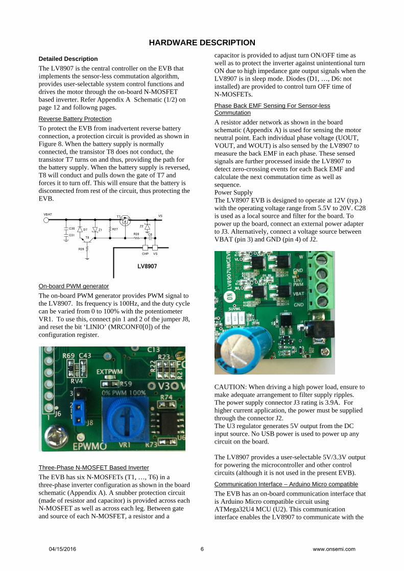
Reverse Battery Protection To protect the EVB from inadvertent reverse battery connection, a protection circuit is provided as shown in Figure 8. When the battery supply is normally connected, the transistor T8 does not conduct, the transistor T7 turns on and thus, providing the path for the battery supply. When the battery supply is reversed, T8 will conduct and pulls down the gate of T7 and forces it to turn off. This will ensure that the battery is disconnected from rest of the circuit, thus protecting the EVB.
VBAT
D7
R26
Z1 R27
T7
R28 C8T8
C30
C31
Z2
CHP VS
LV8907
VS
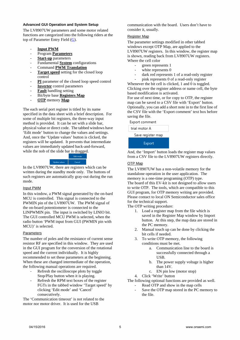
On-board PWM generator The on-board PWM generator provides PWM signal to the LV8907. Its frequency is 100Hz, and the duty cycle can be varied from 0 to 100% with the potentiometer VR1. To use this, connect pin 1 and 2 of the jumper J8, and reset the bit ‘LINIO’ (MRCONF0[0]) of the configuration register.
Three-Phase N-MOSFET Based Inverter The EVB has six N-MOSFETs (T1, …, T6) in a three-phase inverter configuration as shown in the board schematic (Appendix A). A snubber protection circuit (made of resistor and capacitor) is provided across each N-MOSFET as well as across each leg. Between gate and source of each N-MOSFET, a resistor and a
capacitor is provided to adjust turn ON/OFF time as well as to protect the inverter against unintentional turn ON due to high impedance gate output signals when the LV8907 is in sleep mode. Diodes (D1, …, D6: not installed) are provided to control turn OFF time of N-MOSFETs.
Phase Back EMF Sensing For Sensor-less Commutation A resistor adder network as shown in the board schematic (Appendix A) is used for sensing the motor neutral point. Each individual phase voltage (UOUT, VOUT, and WOUT) is also sensed by the LV8907 to measure the back EMF in each phase. These sensed signals are further processed inside the LV8907 to detect zero-crossing events for each Back EMF and calculate the next commutation time as well as sequence. Power Supply The LV8907 EVB is designed to operate at 12V (typ.) with the operating voltage range from 5.5V to 20V. C28 is used as a local source and filter for the board. To power up the board, connect an external power adapter to J3. Alternatively, connect a voltage source between VBAT (pin 3) and GND (pin 4) of J2.
CAUTION: When driving a high power load, ensure to make adequate arrangement to filter supply ripples. The power supply connector J3 rating is 3.9A. For higher current application, the power must be supplied through the connector J2. The U3 regulator generates 5V output from the DC input source. No USB power is used to power up any circuit on the board. The LV8907 provides a user-selectable 5V/3.3V output for powering the microcontroller and other control circuits (although it is not used in the present EVB).
Communication Interface – Arduino Micro compatible The EVB has an on-board communication interface that is Arduino Micro compatible circuit using ATMega32U4 MCU (U2). This communication interface enables the LV8907 to communicate with the
04/15/2016 6 www.onsemi.com
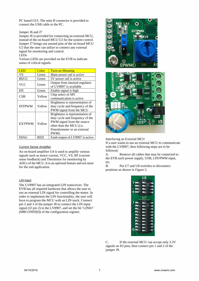
PC based GUI. The mini B connector is provided to connect the USB cable to the PC. Jumper J6 and J7 Jumper J6 is provided for connecting an external MCU, instead of the on-board MCU U2 for the system control. Jumper J7 brings out unused pins of the on-board MCU U2 that the user can utilize to connect any external signal for monitoring and control. LEDs Various LEDs are provided on the EVB to indicate status of critical signals. LED Color Turn-on Meaning VS Green Main power rail is active REG5 Green 5V power rail is active
VCC Green Output from internal regulator of LV8907 is available
EN Green Enable signal is high
CSB Yellow Chip select of SPI communication is active
INTPWM Yellow Brightness is representation of duty cycle and frequency of the PWM signal from the MCU
EXTPWM Yellow
Brightness is representation of duty cycle and frequency of the PWM signal from the source other than the MCU (i.e. Potentiometer or an external PWM)
DIAG RED Fault output of LV8907 is active
Current Sense Amplifier An on-board amplifier U4 is used to amplify various signals such as motor current, VCC, VS, RF (current sense feedback) and Thermistor for monitoring by ADCs of the MCU. It is an optional feature and not must for the end application.
LIN Input The LV8907 has an integrated LIN transceiver. The EVB has all required hardware that allows the user to use an external LIN signal for controlling the motor. In order to implement the LIN functionality, the user will have to program the MCU with an LIN stack. Connect pin 2 and 3 of the jumper J8 to connect the LIN input signal (J2 pin 2) to the LV8907, and set the bit ‘LINIO’ (MRCONF0[0]) of the configuration register.
Interfacing an External MCU If a user wants to use an external MCU to communicate with the LV8907, then following steps are to be followed. A. Remove all cables that may be connected to the EVB such power supply, USB, LIN/PWM input, etc. B. Put U7 and U8 switches to disconnect positions as shown in Figure 5.
C. If the external MCU can accept only 3.3V signals on IO pins, then connect pin 1 and 2 of the jumper J9.
04/15/2016 7 www.onsemi.com
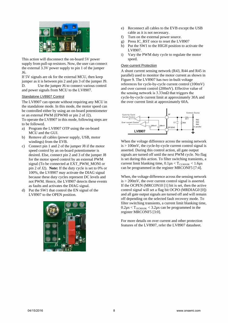
This action will disconnect the on-board 5V power supply from pull-up resistors. Now, the user can connect the external 3.3V power supply to pin 1 of the jumper J6. If 5V signals are ok for the external MCU, then keep jumper as it is between pin 2 and pin 3 of the jumper J9. D. Use the jumper J6 to connect various control and power signals from MCU to the LV8907.
Standalone LV8907 Control The LV8907 can operate without requiring any MCU in the standalone mode. In this mode, the motor speed can be controlled either by using an on-board potentiometer or an external PWM (EPWMI or pin 2 of J2). To operate the LV8907 in this mode, following steps are to be followed. a) Program the LV8907 OTP using the on-board
MCU and the GUI. b) Remove all cables (power supply, USB, motor
windings) from the EVB. c) Connect pin 1 and 2 of the jumper J8 if the motor
speed control by an on-board potentiometer is desired. Else, connect pin 2 and 3 of the jumper J8 for the motor speed control by an external PWM signal (To be connected at EXT_PWM_MONI or pin 2 of J2). Note: If the duty cycle is set to 0% or 100%, the LV8907 may activate the DIAG signal because these duty cycles represent DC levels and not PWM. Hence, the LV8907 detects these events as faults and activates the DIAG signal.
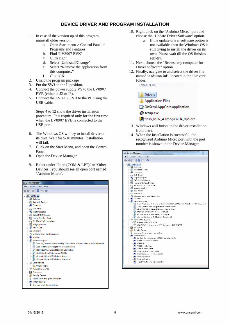
d) Put the SW1 that control the EN signal of the LV8907 to the OPEN position.
e) Reconnect all cables to the EVB except the USB
cable as it is not necessary. f) Turn on the external power source. g) Press IC_RST once to reset the LV8907 h) Put the SW1 to the HIGH position to activate the
LV8907. i) Vary the PWM duty cycle to regulate the motor
speed.
Over-current Protection A shunt current sensing network (R43, R44 and R45 in parallel) used to monitor the motor current as shown in Figure 9. The LV8907 has two in-built voltage references for cycle-by-cycle current control (100mV) and over current control (200mV). Effective value of the sensing network is 3.33mΩ that triggers the cycle-by-cycle current limit at approximately 30A and the over current limit at approximately 60A.
+
-
+
-
200mV 100mV
RF
RFSENS
LV8907
Cycle-by-Cycle Current Control
Over-current Control C7
R17 R43R44R45
in parallel
R29
Common Source
When the voltage difference across the sensing network is > 100mV, the cycle-by-cycle current control signal is asserted. During this control action, all gate output signals are turned off until the next PWM cycle. No flag is set during this action. To filter switching transients, a current limit blanking time, 0.1µs < TCLMASK < 1.6µs can be programmed in the register MRCONF5 [7:4]. When, the voltage difference across the sensing network is > 200mV, the over current control signal is asserted. If the OCPEN (MRCON10 [1] bit is set, then the active control signal will set a flag bit OCPO (MRDIAG0 [0]) and all gate output signals are turned off and will remain off depending on the selected fault recovery mode. To filter switching transients, a current limit blanking time, 0.2µs < TOCMASK < 3.2µs can be programmed in the register MRCONF5 [3:0]. For more details on over current and other protection features of the LV8907, refer the LV8907 datasheet.
04/15/2016 8 www.onsemi.com
DEVICE DRIVER AND PROGRAM INSTALLATION
1. In case of the version up of this program, uninstall older version
a. Open Start menu > Control Panel > Programs and Features
b. Find ‘LV8907 EVK’ c. Click right d. Select ‘Uninstall/Change’ e. Select “Remove the application from
this computer.” f. Clik ‘OK’
2. Unzip the program package 3. Put the SW1 to the L position. 4. Connect the power supply VS to the LV8907
EVB (either at J2 or J3). 5. Connect the LV8907 EVB to the PC using the
USB cable.
Steps 4 to 12 show the driver installation procedure. It is required only for the first time when the LV8907 EVB is connected to the USB port.
6. The Windows OS will try to install driver on
its own. Wait for 5-10 minutes. Installation will fail.
7. Click on the Start Menu, and open the Control Panel.
8. Open the Device Manager.
9. Either under ‘Ports (COM & LPT)’ or ‘Other Devices’, you should see an open port named ‘Arduino Micro’.
10. Right click on the ‘Arduino Micro’ port and choose the ‘Update Driver Software’ option.
a. If the update driver software option is not available, then the Windows OS is still trying to install the driver on its own. Please wait till the OS finishes self-try.
11. Next, choose the "Browse my computer for Driver software" option.
12. Finally, navigate to and select the driver file named ‘arduino.inf’, located in the ‘Drivers’ folder.
13. Windows will finish up the driver installation
from there. 14. When the installation is successful, the
recognized Arduino Micro port with the port number is shown in the Device Manager
04/15/2016 9 www.onsemi.com

15. Run setup.exe of the installation package
16. Launch the program
04/15/2016 10 www.onsemi.com
• Programming the MCU When the firmware of the on-board MCU must be updated, following steps are to be followed. Basically, the firmware is pre-loaded before shipment.
i. Ensure that the EVB is powered up and the USB cable is connected.
ii. Note down the COM port number of the Arduino Micro from the Device Manager window.
iii. Launch ‘flash_MD2_ATmega32U4_0p6.exe’. (The name of this file will be changed based on the revision.)
iv. Two windows will open.
v. Select the COM port from the drop-down menu to ensure that it matches with the COM port as noted in step (ii).
vi. Click ‘Flash’. vii. Programming of the on-board MCU is
initiated.
In case programming fails, unplug and re-plug the board, and re-launch the application. It may be because the required driver was not installed during first attempt.
viii. If the user want to program the MCU with their own source code, then use the on-board ICSP interface (refer schematic in Appendix A) to program the MCU with an external programmer.
04/15/2016 11 www.onsemi.com
APPENDIX A SCHEMATIC (1/2)
04/15/2016 12 www.onsemi.com
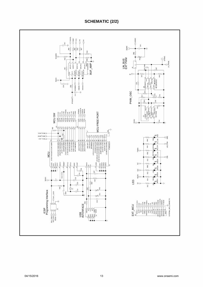
SCHEMATIC (2/2)
04/15/2016 13 www.onsemi.com
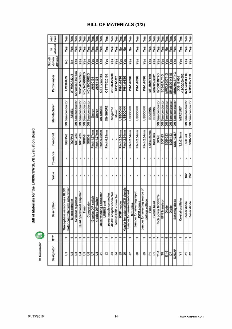
BILL OF MATERIALS (1/3)
04/15/2016 14 www.onsemi.com
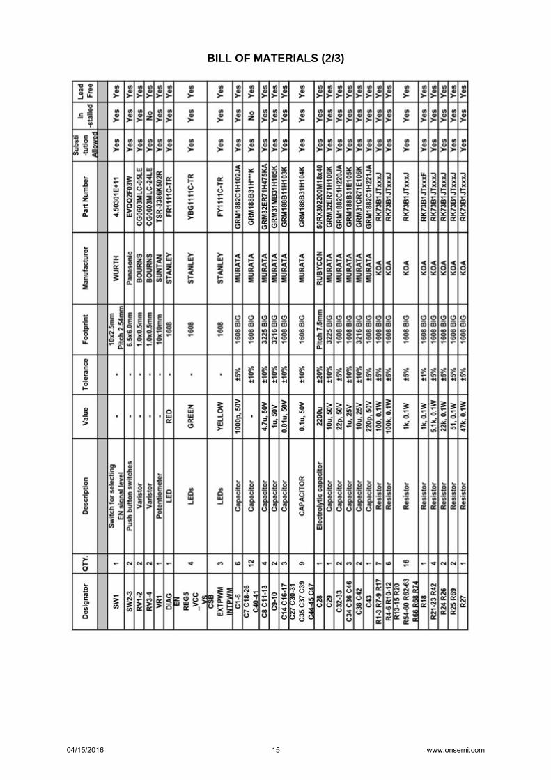
BILL OF MATERIALS (2/3)
04/15/2016 15 www.onsemi.com
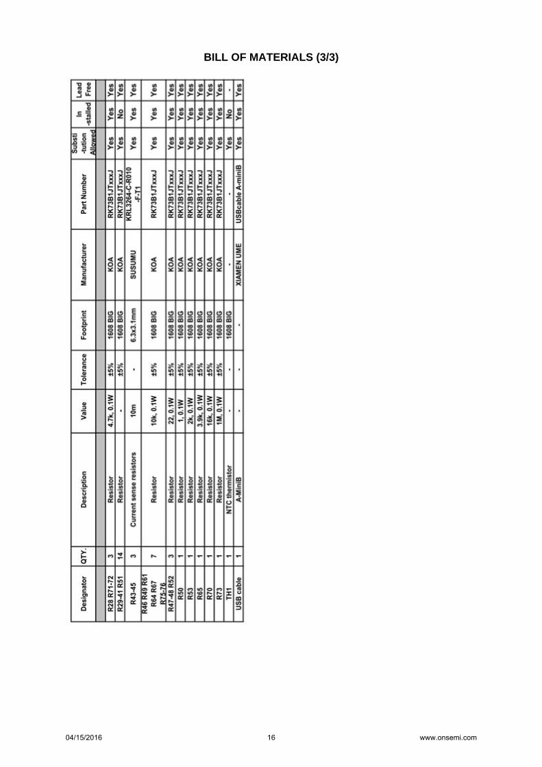
BILL OF MATERIALS (3/3)
04/15/2016 16 www.onsemi.com

ON Semiconductor and the ON logo are registered trademarks of Semiconductor Components Industries, LLC (SCILLC) or its subsidiaries in the United Statesand/or other countries. SCILLC owns the rights to a number of patents, trademarks, copyrights, trade secrets, and other intellectual property. A listing ofSCILLC’s product/patent coverage may be accessed at www.onsemi.com/site/pdf/Patent-Marking.pdf . SCILLC reserves the right to make changes withoutfurther notice to any products herein. SCILLC makes no warranty, representation or guarantee regarding the suitability of its products for any particular purpose,nor does SCILLC assume any liability arising out of the application or use of any product or circuit, and specifically disclaims any and all liability, includingwithout limitation special, consequential or incidental damages. “Typical” parameters which may be provided in SCILLC data sheets and/or specifications canand do vary in different applications and actual performance may vary over time. All operating parameters, including “Typicals” must be validated for eachcustomer application by customer’s technical experts. SCILLC does not convey any license under its patent rights nor the rights of others. SCILLC products arenot designed, intended, or authorized for use as components in systems intended for surgical implant into the body, or other applications intended to support orsustain life, or for any other application in which the failure of the SCILLC product could create a situation where personal injury or death may occur. ShouldBuyer purchase or use SCILLC products for any such unintended or unauthorized application, Buyer shall indemnify and hold SCILLC and its officers,employees, subsidiaries, affiliates, and distributors harmless against all claims, costs, damages, and expenses, and reasonable attorney fees arising out of,directly or indirectly, any claim of personal injury or death associated with such unintended or unauthorized use, even if such claim alleges that SCILLC wasnegligent regarding the design or manufacture of the part. SCILLC is an Equal Opportunity/Affirmative Action Employer. This literature is subject to allapplicable copyright laws and is not for resale in any manner.
04/15/2016 17 www.onsemi.com