Embed Size (px)
Citation preview

I
DMC11 I PL synchronous , line unit
maintenance manual
I

DMC11 IPL synchronous line unit maintenance manual
EK-DMCLU-MM-002
digital equipment corporation • maynard, massachusetts

1 st Edition, April 1977 2nd Printing (Rev), July 1978
Copyright © 1977,1978 by Digital Equipment Corporation
The material in this manual is for informational purposes and is subject to change without notice.
Digital Equipment Corporation assumes no responsibility for any errors which may appear in this manual.
Printed in U.S.A.
This document was set on DIGITAL's DECset-8000 computerized typesetting system.
The following are trademarks of Digital Equipment Corporation, Maynard, Massachusetts:
DIGITAL DEC PDP DECUS UNIBUS
D ECsystem-l 0 DECSYSTEM-20 DIBOL EDUSYSTEM VAX VMS
MASSBUS OMNIBUS OS/8 RSTS RSX lAS

CHAPTER 1
1.1 1.2 1.3 1.4 1.4.1 1.4.2 1.4.3 1.4.4 1.4.5 1.4.6 1.5 1.5.1 1.5.2 1.5.3 1.5.4
CHAPTER 2
2.1 2.2 2.3 2.4 2.5 2.6 2.6.1 2.6.2 2.6.2.1 2.6.2.2 2.6.3 2.7
CHAPTER 3
3.1 3.2 3.3
CONTENTS
Page
INTRODUCTION
SCOPE ................................................................................................................ 1-1 DMCll LINE UNIT GENERAL DESCRIPTION ............................................ .1-1 DMCll LINE UNIT SPECIFICATIONS ........................................................... 1-2 GENERAL DESCRIPTION ............................................................................... 1-3
Introduction ................................................................................................. 1-3 Operating Modes .......................................................................................... 1-4 Microprocessor - Line Unit Data Path ........................................................ .1-4 Transmitter .................................................................................................. 1-5 Receiver ....................................................................................................... 1-5 Signal Conversion and Maintenance Logic ................................................... 1-6
BASICS OF CYCLIC REDUNDANCY CHECKING ...................................... .1-6 Mathematical Background ........................................................................... 1-6 Hardware Implementation of CRC ..... , .......................................................... 1-8 CRC Operation in DDCMP Mode ............................................................... 1-8 CRC Operation in Bit Stuff Mode ............................................................... .1-8
INSTALLATION
SCOPE ................................................................................................................ 2-1 UNPACKING AND INSPECTION ................................................................... 2-1 PREINST ALLATION SETUP PROCEDURES ................................................. 2-2 INSTALLATION AND CHECKOUT ............................................................... 2-7 JUMPER AND SWITCH CHECKLIST ............................................................. 2-8 LOCAL LINK CABLE ...................................................................................... 2-10
Selection ..................................................................................................... 2-1 0 Installation ................................................................................................. 2-11
Connectors ......................... "' .............................................................. 2-12 Grounding ...................................................................... n .................. 2-14
Maintenance ............................................................................................... 2-15 FULL-DUPLEXjHALF-DUPLEX OPERATION ........................................... 2-15
PROGRAMMING
INTRODUCTION .............................................................................................. 3-1 REGISTERS AND DEVICE ADDRESS SELECTION ..................................... 3-1 REGISTER BIT ASSIGNMENTS ...................................................................... 3-1
iii

3.3.1 3.3.2 3.3.3 3.3.4 3.3.5 3.3.6 3.3.7 3.4
CHAPTER 4
4.1 4.2 4.2.1 4.2.1.1 4.2.1.2 4.2.1.3 4.2.1.4 4.2.1.5 4.2.1.6 4.2.1.7 4.2.2 4.2.2.1 4.2.2.2 4.2.2.3 4.2.2.4 4.3 4.3.1 4.3.2 4.3.2.1 4.3.2.2 4.3.2.3 4.3.2.4 4.3.2.5 4.3.2.6 4.3.2.7 4.3.2.8 4.3.3 4.3.4 4.3.5 4.3.5.1 4.3.5.2 4.3.5.3
CONTENTS (Cont)
Page
Data Silo Registers ....................................................................................... 3-3 Out Control Register .................................................................................... 3-3 In Control Register ....................................................................................... 3-6 Modem Control Register .............................................................................. 3-7 Sync Register ................................................................................................. 3-9 Switch Selectable Registers (R15 and RI6) .................................................... 3-9 Maintenance Register ................................................................................... 3-9
PROGRAMMING PROCEDURES ................................................................. 3-10
DETAILED DESCRIPTION
4-1 INTRODUCTION .............................................................................................. 4-1 FUNCTIONAL DESCRIPTION ....................................................................... .4-3
Logic Description ......................................................................................... 4-3 Registers .............................................................................................. 4-3 Out Control Logic ................................................................................ 4-4 In Control Logic ................................................................................... 4-4 Transmitter Control Logic ................................................................... .4-4 Receiver Control Logic ......................................................................... 4-5 CRC Logic ............................................................................................ 4-6 Data Set Interface Logic ....................................................................... 4-7
Major Operating Features ............................................................................ 4-7 Introduction ......................................................................................... 4-7 Modem Control ................................................................................... 4-7 Transmitter Section .............................................................................. 4-7 Receiver Section ................................................................................. 4-10
DETAILED DESCRIPTION ............................................................................ 4-12 Introduction ............................................................................................... 4-12 Registers ..................................................................................................... 4-12
In Data Silo Register .......................................................................... 4-12 Out Data Silo Register ........................................................................ 4-14 Output Control Register .................................................................... .4-17 Input Control Register ........................................................................ 4-19 Modem Control Register .................................................................... 4-21 Sync Register ...................................................................................... 4-23 Reserved Switch Registers (R 15 and R 16) ........................................... 4-23 Maintenance Register ........ , ................................................................ 4-23
Out Control Logic ...................................................................................... 4-24 In Bus Control Logic .................................................................................. 4-26 Transmitter Control Logic .......................................................................... 4-29
ROMs and ROM Sync Buffer ............................................................ .4-29 TX Clock Logic .................................................................................. 4-34 TD Flip-Flop and Is Counter ............................................................. 4-37
IV

4.3.5.4 4.3.5.5 4.3.5.6 4.3.5.7 4.3.5.8 4.3.6 4.3.6.1 4.3.6.2 4.3.6.3 4.3.6.4 4.3.6.5 4.3.6.6 4.3.7 4.3.7.1 4.3.7.2 4.3.7.3 4.3.7.4 4.3.7.5 4.3.8 4.3.8.l 4.3.8.2 4.3.8.3 4.3.9 4.3.9.1 4.3.9.2 4.3.9.3 4.3.l0 4.3.l1 4.3.l1.1 4.3.11.2 4.3.11.3
CHAPTER 5
5.1 5.2 5.3 5.4 5.5 5.5.1 5.5.1.1 5.5.1.2 5.5.1.3 5.5.2
CO NTENTS (Cont)
Page
Transmitter Character Serialization Counter (TCSC) ......................... .4-39 SACT, DONE, and DATA LATE Flip-Flops .................................... .4-40 Transmitter Shift Register (Print D7) ................................................. .4-43 SFG Flip-Flop and Underrun Recovery Circuit (Auto Silo Flush) ..... .4-44 Half-Duplex Fail Safe Circuit (M8202 Only) ...................................... .4-45
Receiver Logic ............................................................................................ 4-46 ROMs and RCS Flip-Flop .................................................................. 4-47 Clock Logic ........................................................................................ 4-49 CFF Flip-Flop and R1BC Counter (Print D10) .................................. .4-52 Shift Register Counter ........................................................................ 4-53 Shift Register and Data Buffer ........................................................... .4-55 In Data Silo ........................................................................................ 4-55
CRC Logic ................................................................................................. 4-57 General .............................................................................................. 4-57 Error Detection Logic ......................................................................... 4-57 Transmitter CRC Register ................................................................. .4-59 Receiver CRC Register ....................................................................... 4-61 Typical CRC Accumulation ............................................................... .4-62
Data Set Interface Logic (M8201 Only) ...................................................... .4-65 General .............................................................................................. 4-65 Conversion of Signals from the Modem .............................................. 4-65 Conversion of Signals to the Modem ................................................... 4-66
Maintenance Logic ..................................................................................... 4-67 General .............................................................................................. 4-67 RC Clock ........................................................................................... 4-68 Maintenance Multiplexers ................................................................. .4-68
Initialization Logic ..................................................................................... 4-71 Integral Modem (M8202 Only) ................................................................... 4-72
General Information ........................................................................... 4-72 Functional Description ....................................................................... 4-72 Detailed Description ........................................................................... 4-76
MAINTENANCE
SCOPE ................................................................................................................ 5-1 MAINTENANCE PHILOSOPHy ...................................................................... 5-1 PREVENTIVE MAINTENANCE ...................................................................... 5-1 TEST EQUIPMENT REQUIRED ...................................................................... 5-1 CORRECTIVE MAINTENANCE ..................................................................... 5-2
Maintenance Modes ..................................................................................... 5-2 Internal Maintenance ........................................................................... 5-2 System Test .......................................................................................... 5-2 External Maintenance Mode ................................................................ 5-2
Troubleshooting Aids ................................................................................... 5-3
v

5.5.2.1 5.5.2.2 5.5.2.3 5.5.3
APPENDIX A
Figure No.
2-1 2-2 2-3 2-4 2-5 3-1 3-2 3-3 3-4 3-5 4-1 4-2 4-3 4-4 4-5 4-6 4-7 4-8 4-9 4-10 4-11 4-12 4-13 4-14 4-15 4-16 4-17 4-18 4-19 4-20 4-21
CONTENTS (Cont)
Page
M8201 Isolation ................................................................................... 5-3 M8202 Isolation ................................................................................... 5-7 Modem Compatibility .......................................................................... 5-8
Sample Waveforms ....................................................................................... 5-8
INTEGRATED CIRCUIT DESCRIPTIONS
FIGURES
Title Page
Jumpers and Switches - M8201 Module ............................................................... 2-2 Jumpers and Switches - M8202 Module ............................................................... 2-3 Local Link Cable Connectors ............................................................................. 2-13 Signal Reflections from a Line Fault ................................................................... 2-16 Full-DuplexjHalf-Duplex Connections .............................................................. 2-17 Line Unit Register Configurations and Bit Assignments ....................................... 3-2 Out Control Register Format ............................................................................... 3-3 In Control Register Format .................................................................................. 3-6 Modem Control register Format .......................................................................... 3-7 Maintenance Register Format .............................................................................. 3-9 Line Unit Simplified Block Diagram .................................................................... 4-2 Logical Representation of3341 FIFO ................................................................ .4-13 Architecture of In Data Silo ................................................................................ 4-15 Logic for Output Control Register Bits 0-4 ........................................................ .4-18 Logic for Output Control Register Bit 7 .............................................................. 4-19 Logic for Input Control Register Bits 0-3 .......................................................... .4-20 Logic for Input Control Bit 7 .............................................................................. 4-21 RTS and DTR Flip-Flops and Associated Drivers .............................................. 4-22 Block Diagram ofOBUS and Associated Logic .................................................. 4-25 Register Decoder ................................................................................................ 4-27 IBUS Control Logic (I-Bit Slice) ........................................................................ 4-28 Transmitter ROMs and Associated Logic .......................................................... .4-31 EIA Transmitter Clock Conversion Logic ........................................................... 4-35 Transmitter Clock Logic and Timing Diagram .................................................. .4-36 TD Flip-Flop and 1 s Counter ............................................................................. 4-38 TCSC Counter ................................................................................................... 4-40 SACT, DONE, and DATA LATE Flip-Flops .................................................... 4-41 Transmitter Shift Register .................................................................................. 4-43 SFG Flip-Flop and U nderrun Recovery Circuit. ................................................ .4-44 Half-Duplex Fail Safe Circuit ............................................................................ .4-46 Receiver ROMs and Associated Logic ................................................................ 4-48
vi

Figure No.
4-22 4-23 4-24 4-25 4-26 4-27 4-28 4-29 4-30 4-31 4-32 4-33 4-34 4-35 4-36 4-37 5-1
5-2
5-3 5-4 5-5 5-6
Table No.
2-1 2-2 2-3 2-4 3-1 4-1 4-2 4-3 4-4 4-5 4-6 4-7 5-1 A-I
FIGURES (Coot)
Title Page
EIA Receiver Clock Conversion Logic ............................................................... .4-50 Receiver Clock Logic and Timing Diagram ....................................................... .4-51 CFF Flip-Flop and RIBC Counter .................................................................... .4-52 Receiver Shift Register Counter ......................................................................... .4-54 Receiver Shift Register and Data Buffer ............................................................. .4-56 CRC Error Detection Logic ................................................................................ 4-58 Transmitter CRC Register .................................................................................. 4-60 Receiver CRC Register ....................................................................................... 4-63 Typical Transmit and Receive CRC Accumulation ............................................ .4-64 Conversion Logic for DSR and CS Signals ........................................................ .4-66 Maintenance Logic ............................................................................................. 4-69 Simplified Block Diagram of Modem Transmitter ............................................. .4-73 Simplified Block Diagram of Modem Receiver ..................................... , ............ .4-75 Schematic and Timing Diagrams for Modem Transmitter Logic ........................ .4-77 Schematic and Timing Diagram for Modem Receiver Logic .............................. .4-82 RESET Retriggerable One-Shot ........................................................................ .4-83 Schematic of H325 Test Connector for DMCll-DA Option (EIA/CCITT V24 Interface) ...................................................................................................... 5-4 Schematic of H3250 Test Connector for DMCII-FA Option (CCITT V.35 Interface) ..................................................................................................... 5-5 Transmitter Output Waveforms for DMCII-MD (56 kHz) Line Unit. .................. 5-9 Transmitter Output Waveforms for DMCII-MA (1 MHz) Line Unit ................. 5-10 Receiver Input Waveforms for DMCII-MD (56 kHz) Line Unit ........................ 5-11 Receiver Input Waveforms for DMCII-MA (1 MHz) Line Unit. ........................ 5-12
TABLES
Title Page
M 820 1 Jumper Configurations .............................................................................. 2-4 M8202 Jumper Configurations ............................................................................. 2-5 Configuration of Switch Pack No.1 ..................................................................... 2-6 Jumper and Switch Checklist ................................................................................ 2-9 Line Unit Registers .............................................................................................. 3-1 Transmitter Function Decode ROM Input Signals ............................................ .4-32 Transmitter Data Path Control ROM Input Signals .......................................... .4-33 Transmitter Data Decode ROM Input Signals ................................................... .4-33 Receiver Decode ROM Input Signals ................................................................ .4-49 Receiver Function ROM Input Signals .............................................................. .4-49 Signals from the Modem ..................................................................................... 4-65 Signals to the Modem ; ........................................................................................ 4-67 Test Equipment Required ..................................................................................... 5-2 Integrated Circuits ......................................................................................... ..... A-l
vii

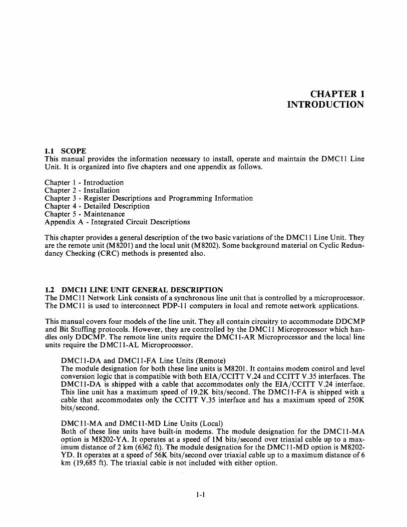
1.1 SCOPE
CHAPTER 1 INTRODUCTION
This manual provides the information necessary to install, operate and maintain the DMCII Line Unit. It is organized into five chapters and one appendix as follows.
Chapter 1 - Introduction Chapter 2 - Installation Chapter 3 - Register Descriptions and Programming Information Chapter 4 - Detailed Description Chapter 5 - Maintenance Appendix A - Integrated Circuit Descriptions
This chapter provides a general description of the two basic variations of the DMCII Line Unit. They are the remote unit (M820l) and the local unit (M8202). Some background material on Cyclic Redundancy Checking (CRC) methods is presented also.
1.2 DMCll LINE UNIT GENERAL DESCRIPTION The DMCII Network Link consists of asynchronous line unit that is controlled by a microprocessor. The DMC 11 is used to interconnect PDP-II computers in local and remote network applications.
This manual covers four models of the line unit. They all contain circuitry to accommodate DDCMP and Bit Stuffing protocols. However, they are controlled by the DMCII Microprocessor which handles only DDCMP. The remote line units require the DMCII-AR Microprocessor and the local line units require the D MC ll-AL Microprocessor.
DMCII-DA and DMCII-FA Line Units (Remote) The module designation for both these line units is M8201. It contains modem control and level conversion logic that is compatible with both EIA/CCITT V.24 and CCITT V.35 interfaces. The DMCll-DA is shipped with a cable that accommodates only the EIA/CCITT V.24 interface. This line unit has a maximum speed of 19.2K bits/second. The DMCII-FA is shipped with a cable that accommodates only the CCITT V.35 interface and has a maximum speed of 250K bits/second.
DMC I1-MA and DMCI1-MD Line Units (Local) Both of these line units have built-in modems. The module designation for the DMCII-MA option is M8202-Y A. It operates at a speed of 1M bits/second over triaxial cable up to a maximum distance of 2km (6362 ft). The module designation for the DMCII-MD option is M8202-YD. It operates at a speed of 56K bits/second over triaxial cable up to a maximum distance of 6 km (19,685 ft). The triaxial cable is not included with either option.
1-1

1.3 DMCll LINE UNIT SPECIFICATIONS
DMCII-MA and DMCll-MD Line Units (Local)
Operating Mode
Data Format
Character Size
Block Check
Data Rate
Maximum Distance DMCII-MA
DMCII-MD
Modulation
Transmitter Timing
Receiver Timing
Line Interface
Common Mode Rejection
Transmitter Signal
Receiver Signal
Connector Type
Mounting Space
Power Consumption
Half-duplex (single cable), Full-duplex (two cables)
Synchronous serial by bit, LSB first
8 bits
16-bit polynomials: CRC-16 and modified CRCCCITT
1,000,000 bits/second (DMCII-MA), 56,000 bits/second (DMCII-MD)
Belden 8232 or equivalent: 1 km (3281 ft) Belden 8233: 2 km (6562 ft)
Belden 8232: 3 km (9843 ft) Belden 8233: 6 km (19,685 ft)
Diphase (double frequency) NRZ
RC Osc., trimmable ± 5%
From received signal
Transformer coupled
500 to 1
4 volts P-P (min.)
150 mV P-P (min.)
AMP 20606X series
One hex SPC slot (DDIIB, C or D), cut out permits use in end slots of backplane as well, provided the Unibus in/out slots contain low height (6.35 cm, 2.5 in) modules like the M930.
3.0 A at +5 V 0.046 A at -15 V 0.018 A at +15 V
DMCll-DA and DMCll-FA Line Units (Remote)
Operating Mode Full- or half-duplex
Communications Channel Private wire or switched
1-2

Data Format
Character Size
Block Check
Data Rate
Interface
Modems
Signals Supported
Cable
Mounting Space
Power Consumption
1.4 GENERAL DESCRIPTION
1.4.1 Introduction
Synchronous, serial by bit, LSB first
8 bits
16-bit polynomials: CRC-16 and modified CRCCCITT
Up to 19,200 bits/second (DMCI1-DA)
Up to 250,000 bits/second (DMCII-FA) using V.35 level conversion, limited by' (DMCII-AR) microcode. Up to 1 M bits/second; limited by hardware.
f{S232C or CCITT V.24 compatible (DMCllDA), CCITT V.35 compatible (DMCII-FA)
Bell 208, 209 or equivalent (DMCII-DA) GTE/Lenkurt L500A-5, WECo. (Bell) 500A Ll/5, or equivalent (DMCII-FA)
BA transmit data DB serial clock transmit (SCT) BB receive data DD serial clock receive (SCR) CC data set ready CD data terminal ready CA request to send CB clear to send CE ring
7.62 m (25 ft) with EIA connector supplied
One hex SPC slot (DDIIB, C, or D), cutout permits use in end slots of backplane as well, provided the Unibus in/out height (~6.35 cm, 2.5 in) modules like the M930.
3.2 A at +5 V 0.31 A at -15 V 0.03 A at +15 V
This section provides a general description of the M8201 andM8202 Line Units. A more detailed description at the function level is contained in Chapter 4, Detailed Description.
1-3

The DMCll Line Units (M8201 and M8202) perform the standard functions associated with a synchronous communications device. They are:
Parallel-to-serial data conversion. Serial-to-parallel data conversion. SYNC character detection. Leading SYNC character stripping.
In addition, the line units can perform the following functions.
Modem control and monitoring Cyclic redundancy character testing. Zero bit stuffing Zero bit stripping A utomatic flag transmission. A utomatic flag recognition. Automatic abort sequence transmission. Automatic abort sequence recognition. Automatic pad character transmission.
1.4.2 Operating Modes The line units may operate in either of two microprogrammable modes. The modes are:
I. DDCMP mode - This is an 8-bit byte mode of operation. It is designed for the highly efficient byte oriented Digital Data Communications Message Protocol (DDCMP) using the CRC-16 polynomial.
NOTE Less efficient character oriented protocols that use many control characters can use this mode of operation but the CRC logic must be disabled. The microprogram within the DMCll Microprocessor would have to compute the CRC.
2. Bit Stuff mode - This is a bit oriented mode of operation. It is designed for the bit oriented message protocols using the flag and abort sequences and the modified CRC-CCITT polynomial.
The line unit provides a data path between the microprocessor and a data set (or local link) and vice versa.
1.4.3 Microprocessor - Line Unit Data Path The following discussion is keyed to the block diagram shown in Figure 4-1.
The microprocessor and line unit communicate through two unidirectional data paths. Signals BALU 0-7 compose the data path from the microprocessor to the line unit. The line unit appears to the microprocessor as eight registers. The data is passed to the correct register by control signals CROM 0-3. Signal OBW is the strobe.
The line unit communicates with the microprocessor through the Line Unit In Bus (LU IBUS). The microprocessor controls all reading of the line unit registers.
Various maintenance signals are passed to the Maintenance and Miscellaneous logic. These signals control the functioning of the receiver and transmitter in the maintenance mode.
1-4

1.4.4 Transmitter The transmitter portion of the line unit consists of three functional groups of logic. They are:
1. Out Data Silo 2. Transmitter Control 3. Transmitter CRC Logic
This logic performs specific parts of the transmission function. The functions are explained below.
The Out Data Silo is seen as a write only register to the microprocessor. The Transmitter Control logic sees it as a buffer. The silo is a 64-word-deep data path between the microprocessor and the Transmitter Control logic.
The hardware implementation of this silo is through the use of FIFO (First In/First Out) devices. The silo effect is necessary because of the speed difference between the serialization process and the data available from the microprocessor. Because of the speed with which the microprocessor could load characters (conceivably, one character every 300 nanoseconds) and the speed at which the characters can be serialized (using dial up facilities, approximately one character every 160 microseconds), there must be a multicharacter buffer. Additionally, in order to relieve the microprogram of the need to have timers to know when to load another message or when to end a message, transmitter control bits Start of Message (SOM) and End of Message (EOM) are siloed also.
A typical sequence of operation is:
1. Microprogram loads Start of Message into the Out Control register. 2. Microprogram loads data into the Out Data Silo. 3. The Transmitter detects SOM at the silo output. 4. Request to Send is asserted by the transmitter, automatically. 5. Clear To Send and Data Set Ready come true. 6. The transmitter is enabled. Serialization begins.
As long as the SOM bit is true, the data beinq serialized is not included in the CRC computation.
When the Tx Control detects a character available from the silo without the SOM bit set, it includes that character, and all the characters following it, in the CRe computation.
When End of Message is detected, the Tx Control transmits the CRC Check Character (called the BCC). If more data follows the EOM, a new CRC computation is begun.
1.4.5 Receiver The receiver portion of the line unit consists of three functional groups of logic. They are:
1. In Data Silo 2. Receiver Control 3. Receiver CRC Logic
This logic performs specific parts of the receive function. The functions are explained below.
The In Data Silo is seen by the microprocessor as a read only register. The Rx Control sees it as an output buffer. The silo is a 64-word-deep data path between the Rx Control and the microprocessor.
The hardware implementation of the silo is similar to that used in the transmitter. Input to the In Data Silo is controlled by the Rx Control while output is controlled by the microprogram. The silo is present for the same reasons mentioned in the discussion of the transmitter.
1-5

A typical sequence of operations is:
I. The receiver becomes active after detecting the first data character preceded by two or more synchronizing sequences (one flag sequence in the case of Bit Stuff mode).
2. ,The data character is included in the CRC computation automatically.
3. The data character is loaded into the silo by the Receive Control.
4. The microprogram detects, by bit testing, both In Active and In Ready (bits 6 and 4, respectively, of the In Control register).
5. The microprogram reads the In Data Silo.
6. The silo presents In Ready with each subsequent character.
7. The microprogram, having determined when the message ends, checks the BCC Match bit (bit 0 of the In Control register). If the bit is set, the message had no detected errors.
8. In Bit Stuff mode, the Block End bit (Bit I of RI2) is set with the BCC Match bit, if no errors were detected.
1.4.6 Signal Conversion and Maintenance Logic The signal conversion and maintenance logic provide automatic modem control, clock sources for the transmitter and receiver, and the receiver data source.
1.5 BASICS OF CYCLIC REDUNDANCY CHECKING
1.5.1 Mathematical Background A cyclic code message consists of a specific number of data bits and a Block Check Character (BCC) that is computed by the CRC logic. Let n equal the total number of bits in the message and k equal the number of data bits; then n-k equals the number of bits in the BCC.
The code message is derived from two polynomials which are algebraic representations of two binary words, the generator polynomial P(X) and the message polynomial G(X). The generator polynomial is the type of code used (CRC-I2, CRC-I6, CRC-CCITT, etc.); the message polynomial is the string of serial data bits. The polynomials are usually represented algebraically by a string of terms in powers of X such as Xn ... + X3 + X2 + X + XO (or I). In binary form, a I is placed in each position that contains a term; absence of a term is indicated by a O. The convention followed in this manual is to place the least significant bit (XO) at the right. For example, if a polynomial is given as X4 + X + I its binary representation is 10011 (3rd and 2nd degree terms are not present).
Given a message polynomial G(X) and a generator polynomial P(X), the objective is to construct a code message polynomial F(X) that is evenly divisible by P(X). It is accomplished as follows.
I. Multiply the message G(X) by Xn-k where n-k is the number of bits in the BCC.
2. The resulting product Xn-k[G(X)] is divided by the generator polynomial P(X).
3. The quotient is disregarded and the remainder C(X) is added to the product to yield the code message polynomial F(X), which is represented as Xn-k[G(X)] + C(X).
1-6

The division is performed in binary without carries or borrows. In this case, the remainder is always one bit less than the divisor. The remainder is the Bee and the divisor is the generator polynomial; therefore, the bit length of the Bee is always one less than the number of bits in the generator polynomial.
A simple example is explained below.
1. Given:
Message polynomial G(X) = 110011 (X5 + X4 + X + XO) Generator polynomial P(X) = 11001 (X4 + X3 + 1) G(X) contains 6 data bits P(X) contains 5 bits and will yield a Bee with 4 bits; therefore, n-k = 4
2. Multiplying the message G(X) by Xn-k gives:
Xn-k[G(X)] = X4(X5 + X4 + X + XO) = X9 + X8 + X5 + X4
The binary equivalent of this product contains 10 bits and is 1100110000.
3. This product is divided by P(X)
P (X)-.11001
100001 ___ quotient
11001100004-- Xn-k [G (X)] 11001
10000 11001
1001 ..... 1--- Remainder=C (X)=BCC
4. The remainder e(X) is added to Xn-k[G(X)] to give F(X) = 1100111001.
The code message polynomial is transmitted. The receiving station divides it by the same generator polynomial. If there is no error, the division will produce no remainder and it is assumed that the message is correct. A remainder indicates an error. The division is shown below.
P(X)--.11001 100001
1100111001 4-- F (X) 11001
11001 11001 00000 ___ no remainder
1-7

1.5.2 Hardware Implementation of eRe The BCC is computed and accumulated in a shift register during transmission. Another shift register is used during reception to examine the received data and BCC. In each register, the number of stages is equal to the degree of the generating polynomial. In the line unit, the registers have 16 stages because 16 degree generating polynomials are used. The Bit Stuff mode uses code CRC-CCITT whose generator polynomial is XI6 + Xl2 + X5 + 1. DDCMP uses code CRC-16 whose generator polynomial is XI6 + XI5 + X2 + 1.
Both the transmitter and receiver CRC registers have control logic that allows the registers to be configured for the selected CRC code.
When a message and accompanying BCC character have been received, the CRC logic only indicates whether the message is in error or not. It does not correct errors nor does it even enumerate or locate errors. Under protocol discipline, the sending station is requested to retransmit the message.
1.5.3 eRe Operation in DneMP Mode Under DDCMP protocol control, CRC operation is exactly like that described in Paragraph 1.3.4.1, Mathematical Background.
The transmitter and receiver CRC registers are initialized to all Os. At the sending station, the transmitter CRC register accepts the information being transmitted and accumulates the BCC. When the last bit of information has been transmitted, the contents of the transmitter CRC register are transmitted.
At the receiving station, the information plus the 16-bit BCC is examined by the receiver CRC register. At the end of the message (information plus BCC), the contents of the receiver CRC register should read 0 if the message is errorless. The CRC error detection logic asserts a flag if the register reads O. If an error is present, the register reads non-O and the flag is not asserted. The line unit does not count characters, so it is the program's responsibility to look for the CRC error flag at the proper time.
1.5.4 eRe Operation in Bit Stuff Mode Under Bit Stuff protocol control, CRC operation is slightly different than that described in Paragraph 1.3.4.1, Mathematical Background. The differences are:
1. The factor Xk (X15 + XI4 ... + X + 1) is added to Xn-k[G(X)] which corresponds to initializing the transmitter CRC register to all Is. This function is equivalent to inverting the first 16 bits of G(X). This allows detection of the addition or deletion of Os at the leading end of the message due to erroneous flag characters.
2. The accumulated BCC, which is called Frame Check Sequence (FSC) in the Bit Stuff mode, is complemented before being transmitted. This results in a unique non-O remainder (0164178) at the receiver. This allows detection of the erroneous addition or deletion of Os at the trailing edge of the message due to errors.
3. At the receiving station, the receiver CRC register is initialized to all Is. The information plus the FCS constitutes the message and it is added to Xk (X15 + XI4 ... + X + 1) and divided by P(X) to give 0164178, if the transmission is errorless. If an error is present, the flag is asserted.
1-8

2.1 SCOPE
CHAPTER 2 INST ALLATION
This chapter provides information for installation and checkout of the M8201 and M8202line units.
2.2 UNP ACKING AND INSPECTION The line unit comes in four versions which are described below.
DMCII-DA (For EIA/CCITT V.24 Interface)
M8201 - Line Unit Module BC08R-l or BC08S-1 - Interconnect Cable BC05C-25 - Modem Cable H325 - Test Connector
DMCII-FA (For CCITT V.35 Interface)
M8201 - Line Unit Module BC08R-l or BC08S-1 Interconnect Cable BC05Z-25 - DSU Cable H3250 - Test Connector
DMCII-MA (Local 1M bits/second)
M8202-YA - Line Unit Module BC08R-l or BC08S-1 Interconnect Cable 12-12528 - Coaxial Test Connector
DMCII-MD (Local 56K bits/second) M8202-YD - Line Unit Module BC08R-l or BC08S-1 - Interconnect Cable 12-12528 - Coaxial Test Connector
NOTE An additional cable may be included with either of the local line units (DMCII-MA and -MD). It is a 30.48 m (100 ft) long coaxial cable that is designated BC03N-AO. This is not part of the DMCl1. It is a DEC catalog item that can be ordered by the customer.
Inspect these parts for visible damage. Report any damage or shortage immediately to the shipper and the DEC representative.
2-1

2.3 PREINSTALLATION SETUP PROCEDURES
NOTE The line unit cannot function without the DMCllAR or -AL Microprocessor (M8200). It is assumed that the microprocessor has been installed and checked out in accordance with Chapter 2, Installation of the Microprocessor manual (EK-DMCMPMM-OOl).
Before installing the line unit, check the jumpers and switches to be sure that they are in the normal configuration. Locations of the switches and jumpers are shown in Figure 2-1 for the M8201 Module and Figure 2-2 for the M8202 Module.
MSB
SWITCH PACK 3 REGISTER 16
SWITCH PACK 2 REGISTER 15
c=J
LSB
c:::::J c::::=:J
L=::J c::::=::!J
L:=::J C=:J
L::J
SWITCH PACK 1
00011100001
C=:J
I c=:::::J
II I: ii Ii ~ ~
W1
Figure 2-1 Jumpers and Switches - M8201 Module
2-2
W5 W2 W3
MK-0309

=F
. M8202 Module d Switches -2 Jumpers an Figure 2-
2-3
MK-0308

I. Jumpers
Jumper Number
WI
W2
W3
W4
W5
The M8201 Line Unit contains five jumpers (WI-W5). The M8202 Line Unit contains six jumpers (WI-W6). The normal jumper configurations are described in Table 2-1 for the M8201 and Table 2-2 for the M8202.
Table 2-1 M8201 Jumper Configurations
Normal Configuration
Installed
Installed
Removed
Installed
Removed
Function
With this jumper installed, the transmitter CRC character is not inverted by the CRC register output gate.
This jumper must be installed to ensure proper operation of codes CRC-16 and CRC-CCITT under the discipline of DDCMP and Bit Stuff protocols.
If the user removes this jumper for some special reason, the Transmitter CRC character is inverted by the CRC register output gate. The diagnostic will fail also.
Jumpers W2 and W3 are used together.
With W2 installed and W3 removed, the modem Data Set Ready line controls the state of signal DI6 MODEM RDYH.
With W3 installed and W2 removed, signal DI6 MODEM RDY H is always asserted. This feature accommodates modems that do not assert Data Set Ready.
Jumpers W4 and W5 are used together.
With W4 installed and W5 removed, signal DI5 RTS H controls the state of the modem Request to Send line.
With W5 installed and W4 removed, the Request to Send line is on continuously. This feature accommodates modems that require this condition.
NOTE If W2-5 jumpers are not installed in the normal configuration, diagnostics will report modem control errors.
2-4

Table 2-2 M8202 Jumper Configurations
Jumper Normal Number Configuration Function
WI Installed With this jumper installed, the transmitter CRC charac-ter is not inverted by the CRC register output gate.
This jumper must be in to ensure proper operation of codes CRC-16 and CRC-CCITT under the discipline of DDCMP and Bit Stuff protocols.
If the user removes this jumper for some special reason, the Transmitter CRC character is inverted by the CRC register output gate. The diagnostic will fail also.
W2,W3 Removed When installed, the modem receiver protection trans-former is disabled. Installation is not recommended.
W4, W5 Removed When installed, the modem transformer protection transformer is disabled. Installation is not recom-mended.
W6 Removed Installed for single cable half-duplex operation only.
2. Switch Packs No.2 and No.3 Switch packs no. 2 and no. 3 are both 8 switch DIPs. Switch pack no. 2 is Register 15 and is installed in location E87 on the M8201 Line Unit and in location E90 on the M8202 Line Unit. Switch pack no. 3 is Register 16 and is installed in location E88 on the M8201 Line Unit and in location E91 on the M8202 Line Unit.
When the line unit module is shipped, all switches in both pack numbers 2 and 3 are OFF. This is the default status (3778).
For both switch pack no. 1 and switch pack no. 2:
Switch OFF = 1. Switch no. 1 = MSB, Switch no. 8 = LSB.
Correct settings of these switches may be verified by examination of ST AT 2 of the diagnostic printout if run with autosize. Check diagnostic listings for which diagnostics support autosize and a detailed description of the status words.
2-5

These switches are a function of the remote load detect feature of the DMCII. After installation, the switches can be positioned to accommodate the user's requirements.
NOTE When used with the DMCII-AR or DMCII-AL Microprocessor, switch pack number 2 is the password and switch pack number 3 is the boot address offset.
For details concerning the use of these switches, refer to Chapter 3 in the microprocessor manual.
3. Switch Pack No.1
Switch Number
2
3
4
Switch pack no. 1 is an 8 switch DIP that is installed in location E26 on the M8201 Line Unit and in location E29 on the M8202 Line Unit.
For the M8201, all switches except no. 5 are used. For the M8202, all switches except no. 4, 5, and 8 are used. The ON and OFF positions and the switch numbers are marked on the package. The switches are the rocker type and are pushed to the desired position.
Table 2-3 describes the normal configuration for switch pack no. I.
Table 2-3 Configuration of Switch Pack No.1
Normal Position
OFF
OFF
OFF
OFF
Function
With SI OFF, signal DI4 GRTP is low which enables the following ROMs.
Transmitter Function Decode ROM Transmitter Data Decode ROM Receiver Decode ROM Receiver Function ROM
During servicing with the automatic module tester, if S 1 is ON, signal DI4 GRTP is high, which disables these ROMs; manufacturing test only.
With S2 OFF, signal D14 NO CRC is low, which allows the CRC function to be enabled.
With S2 ON, the CRC function is inhibited.
With S3 OFF, signal D14 SEC MODE is low which inhibits operation of the line unit in the secondary mode. This mode is applicable only in the Bit Stuff protocols.
With S4 OFF, Received Data, Modem Receive Clock, and Modem Transmit Clock are presented to the line unit through the EIA/CCITT V.24 interface.
2-6

Table 2-3 Configuration of Switch Pack No.1 (Cont)
Switch Number
Normal Position Function
5
6
7
8
OFF
OFF
Module Dependent
ON
With S4 ON, these signals are received through the CCITT V.35 interface.
This switch is used only on the M8201 Line Unit.
Not Used
Reserved
Signal D14 SW is associated with this switch. It is read only bit 1 of the Modem Control Register. It is read by the diagnostics and indicates the type of line unit.
With an M8201 Line Unit, S7 should be ON (D 14 SW is low).
With an M8202 Line Unit, S7 should be OFF (D14 SW is high).
With S8 ON, the internal RC clock is sent to the modem cable connector (J1) on the M8201 Line Unit.
During servicing with the H325 or H3250 test connector installed on the modem cable, the RC clock is sent back to the line unit as the transmit and receive clocks.
During normal operation, the switch should remain ON.
This switch is used only on the M8201 Line Unit.
2.4 INSTALLATION AND CHECKOUT The M8201 and M8202 Line Units are hex modules that do not interface with the Unibus. The corner of the module in the vicinity of the A and B connectors has been removed. This allows the M8201 or M8202 to be installed in the end slots of the DDll-B, C, or D System Interfacing Units. The module plugs into connectors C, D, E, and F and fits over the Unibus cable connectors and short length (approximately 6.35 cm, 2.5 in) Unibus terminator that are installed in connectors A and B.
Proceed with the installation and checkout as follows.
1. Install the M8201 or M8202 Line Unit and check ± 15 V and +5 V supplies.
2. Interconnect the line unit and the microprocessor using cable BC08R-l or BC08S-1 which is a 0.305 m (one foot) long 40 connector flat mylar cable with H856 female connectors on each end. The mating connector on the microprocessor and line unit is an H854 male connector. On the microprocessor this connector is designated Jl. On the M8201 Line Unit it is designated J2 and on the M8202 Line U nit it is Jl.
2-7

3. On the M8201 Line Unit, install the modem (DSU) cable to connector 11. For the DMCllDA Line Unit, use the BC05C-25 cable. For the DMCII-FA Line Unit, use the BC05Z-25 cable. On the other end of this cable, install the test connector. Use the H325 connector for the BC05C-25 cable and the H3250 connector for the BC05Z-25 cable, with SP1, switch 4 on.
On the M8202 Line Unit, install the 12-12528 coaxial test connector which ties the two coaxial pig-tails together. These two 0.915 m (3 foot) cables are soldered to the M8202.
4. Run MAINDEC-II-DZDME and DZDMF to verify correct line unit operation.
5. The M8201 (DMCII-DA or FA) line unit and the M8200-Y A (DMCII-AR) microprocessor, or the M8202-YA through YD (DMCll-MA through MD) line unit and the M8200-YB (DMCII-AL) microprocessor run the MAINDEC-ll-DZDMG to verify the correct microcode, and MAINDEC-II-DZDMH to verify the operation of the line unit and the microprocessor working together.
6. Remove the test connector from the modem (DSU) cable.
M8201 - For the DMCII-DA, connect the BC05C-25 Cinch connector to the customer supplied modem. For the DMCll-FA, connect the BC05Z-25 Winchester connector to the customer supplied DSU.
M8202 - Connect the coaxial pig-tails to the customer supplied coaxial cables or the BC03N-AO cable.
CAUTION The maximum allowable length for the BCOSC or BCOSZ cable is 15.24 m (SO ft).
2.5 JUMPER AND SWITCH CHECKLIST Table 2-4 represents a concise checklist of the M8201 and M8202 Line Unit switch settings andjumper configuration as shipped.
2-8

Table 2-4 Jumper and Switch Checklist
NOTES:
Jumper Designation
WI W2 W3 W4 W5 W6
SI S2 S3 S4 S5 S6 S7 S8
SI-S8
Jumper Configuration
DMCII-DA DMCII-FA M8201 M8201
IN IN IN IN OUT OUT IN IN OUT OUT NA NA
Settings for Switch Pack No. 1
OFF OFF OFF OFF OFF OFF ON ON
OFF OFF OFF ON OFF OFF ON ON
Settings for Switch Pack Nos. 2 and 3
OFF OFF
I. Switch Pack Locations
SPI-E26 on M8201 and EI9 on M8202 SP2-E87 on M8201 and E90 on M8202 SP3-E88 on M8201 and E91 on M8202
DMCII-MA/MD M8202
IN OUT OUT OUT OUT IN FOR HD
OFF OFF OFF OFF OFF OFF OFF OFF
OFF
2. All switches OFF in SP2 and SP3 represents the default status. Reference the DMCII Microprocessor Manual for details on the use of these switches.
2-9

2.6 LOCAL LINK CABLE This section discusses the selection, installation, and maintenance of the local link cable. This cable serves two purposes. It must deliver the generated signal to the receiver with sufficient amplitude to exceed the receiver threshold and it must shield the signal from external electrical noise.
2.6.1 Selection DIGITAL does not sell cables over 100 ft for use with the DMCll-MA and DMCll-MD integral modem line units. DIGITAL recommends Belden 8232 for runs up to f km with the DMCll-MA, and 3 km with the DMCll-MD. Belden 8233 is recommended for longer runs; up to 2 km with the DMCll-MA, and 6 km with the DMCll-MD. Both cables are double shielded (triaxial). The electrical characteristics listed below are maximum/nominal values.
NOTE The cable should be provided and installed by the customer.
Inductance
Capacitance
Vel. of Prop.
Impedance
Voltage Rating
Sweep Test
Center Conductor DC Resistance Belden 8232
Belden 8233
Shield DC Resistance Belden 8232
Belden 8233
Physical Requirements
0.318 microhenry /meter (0.097 microhenry /ft)
56.7 pF /meter (17.3 pF /ft)
78%
75 ohms
175 Vrms
22 dB min.
l120hms/km (35 ohms/lOOO ft)
8.50hms/km (2.6 ohms/lOOO ft)
8.53 ohms/km (2.6 ohms/lOOO ft)
4.60hms/km (1.4 ohms/lOOO ft)
Triaxial, cellular polyethylene insulation, braid shield, and minimum of 20 A WG center conductor
2-10

The cable used must be 75 ohms impedance type. The maximum total dc resistance for the cable shield and center conductor must be less than 200 ohms for the DMCII-MA, and 400 ohms for the DMCllMD. The maximum total capacitance from the shield to the center conductor must be less than 0.14 ~F for the DMCII-MA and 0.4 ~F for th DMCII-MD. The double shield provides excellent noise rejection when properly grounded. The cellular polyethylene dielectric provides low signal loss and low distortion. The polyethylene jacket has excellent weather and abrasion resistance.
NOTE Typical cables using 20 AWG copper weld center conductors vary from 35 to 70 ohms dc resistance. Use of dc resistance over 35 ohms per 1000 ft severely derates the maximum length of the cable. The longer cable must use solid copper, 14 AWG.
When selecting cable, several factors must be considered in determining cable attenuation. The value given by the cable vendor is for room temperature and is nominal, being subject to deviation up to 20 percent. The attenuation increases with temperature at approximately 0.20 percent per degree Celsius (0.11 percent per degree Fahrenheit). At 50° C (122° F) an additional loss of 5 percent over the room temperature specification can be expected. Finally, use at elevated temperatures causes aging at a faster than normal rate and, after 5 years, could produce yet another permanent 10 percent increase in attenuation. Thus the initial nominal 8.53 dB/km (2.6 dB/ 1000 ft) loss could become, after 5 years use at high temperature, 17.06 dB/km (5.2 dB/I000 ft) worst case.
2.6.2 Installation The characteristics of the local link cable should be measured prior to installation. In particular, there are two parameters that the user should measure and note for future reference. These are the propagation time delay, which can be measured with a pulse generator and an oscilloscope, and the dc resistance of the cable with the far end of the center conductor shorted to the inner shield. For the Belden 8232, these parameters can be expected to be nominally 4.26 ns/m (1.30 ns/ft) and 105 ohms/km (320hms/l000 ft). For Belden 8233, these paramters can be expected to be nominally 4.26 ns/m (1.30 ns/ft) and 13 ohms/km (4 ohms/ 1000 ft). Once the cable is installed, and both ends are therefore not available at the same place, the latter parameter can still be measured easily, and the former can be measured by use of the TDR method described in Paragraph 2.6.3.
While installing the cable, make a complete map of its layout, showing the position of the cable with respect to buildings, equipment and so forth, and also the locations of all access points, including not only splices and in-line connectors, but pull boxes also. Carefully measure and record cable lengths between landmarks. Such a map will greatly facilitate maintenance.
The user must take the following factors into account when installing the local link cable.
TEMPERATURE - The polyethylene used as the dielectric material in most coaxial and triaxial cables begins to soften above 80° C. As the conductor moves off center, variations in cable characteristics occur. If installed under tension with sharp bends, the conductor may short to the shield. Additionally, the open circuit resistance should be measured after installation to ensure against shorts incurred during installation. This resistance should be ~ 20 Kilohms. The closed circuit resistance should be 118.4 ohms/km (36.1 ohms/l000ft).
MOISTURE - Moisture or moisture-related impurities may enter the cable through cuts or scratches in the outer jacket or through improperly installed connectors. Minute amounts of water vapor will condense into water, which can migrate along the braid. Water condensed from a polluted atmosphere can contaminate the entire length of cable, shorten its lifetime, and seriously degrade performance.
2-11

PULLING TENSION - For most environmental conditions, it is generally preferred that the cable be installed in conduit, through which the cable must be pulled. During installation, the total pulling tension on the 20 A WG center conductor must not exceed 8.8N (2 pounds).
For ease in maintenance, it is best to divide the cable into sections. For long cable runs in conduit, it is convenient to have a pull box every 30.48 m (100 ft) or equivalent. A 90 degree conduit bend is equal to 9.15 m (30 ft) of straight level conduit. It is recommended that an antifriction agent be used during pulling, provided the agent is compatible with the cable jacket material.
SPLICES AND CONNECTORS - The cable layout should provide access points for test purposes and for replacing defective sections. (See Paragraph 2.6.2.1.) Strain relief must be provided at all splices and in-line connectors.
RECOMMENDED WIRING PRACTICES - Chapter 8, Article 800 of the National Electric Code defines wiring rules for communications circuits. These rules must be observed for safe operation of the DMCII. In particular, note these provisions of the code:
"Communication conductors shall not be placed in a raceway, compartment, outlet box, junction box or similar fitting with conductors for light and power. . ."
"Communication conductors may be run in the same shaft with conductors for light and power provided the conductors of the two systems are separated by at least two inches."
"Suitable protective devices must be employed for wiring between buildings."
SURGE WITHSTAND CAPABILITY - The receiver has no provision for protection against normal mode voltage surges exceeding 30 V. If surge withstand is required, the user must install a separate circuit to condition signals to the receiver.
NOISE - The M8202 is designed to operate with a common mode rejection ratio > 500: 1. Cable selection, installation grounding and noise suppression are means of reducing line error rates.
2.6.2.1 Connectors - The following components are recommended for use in joining cable sections and also for connecting the cable to the M8202 pigtails. All of these components, which are shown in Figure 2-3, are manufactured by AMP Inc., Harrisburg, Pennsylvania.
Component Digital Part Number AMP Part No.
Cable clamp 12-11430 206062-1
Male housing 12-12527 206153-1
Male pin 12-12001 66589-2
Female housing 12-12526 206060-1
Female pin 12-12000 66590-2
14 ga male pin 12-12001-1 66587-2
The connectors are installed by crimping the pins to the cable; the recommended crimper is the AMP Type VI, 90277-1. It is very unlikely that one can install a set of connectors without requiring the use of an ejector, to remove pins that have been inserted incorrectly; the proper ejector for the above pins is the AMP 305183.
2-12

~ CLAMP
FEMALE
~LE PINS
TRIAX OUTER SHIELD FOR GROUND CONNECTION
AT COMPUTER END
~LE PINS
MK-0292
Figure 2-3 Local Link Cable Connectors
The pin holes in the housing and receptacle are numbered. When working with a connector, always orient it so that hole 1 is at the top, then hole 4 is at the bottom, and the holes on either side are 2 and 3.
1. The cable clamp assembly is supplied as a shell, two screws, and three clamps, of which the one for the largest cable size should be used. Slide the shell onto the cable.
2. Dress the center conductor back enough so it will fit into a pin with the pin crimped to its insulation as well as to the conductor. Dress both shields back about another half inch, and taper the final half inch of the inner insulation so that its tip fits into the pin, and about a quarter inch fits into the connector, along with the center conductor. Crimp the pin to both the conductor and its insulation, and insert the pin in hole 1.
3. Separate the inner shield into two parts, attach pins to them, and insert the pins into holes 2 and 3.
4. Pull the outer shield together, insulate it from the inner shield, crimp a pin to it, and insert the pin ih hole 4 for splicing connections. The end connectors should have the outer shield brought out of the shell and tied to the grounded wire.
5. Screw the shell into the housing, and screw the clamp to the shell.
6. After male and female connectors have been plugged together, screw the other ring of the female housing over the male housing.
2-13

Both M8202 pigtails have female connectors, therefore, the local link cable must have a male connector. The connectors at the ends of the cables are installed in the same manner described above except that at the ends the outer shield must be grounded as described in Paragraph 2.6.2.2. The male connector shown in Figure 2-3 is made up for a spliced connection. The wire sticking out the back end of the connector is the outer shield, which must be grounded.
2.6.2.2 Grounding -This paragraph describes the proper grounding techniques that must be used to prevent the possibility of personal injury.
There is a possibility of a difference in ground potential between two computers that are separated by some distance, especially if they are powered from different sockets.
If in doubt about the recommendations in this paragraph, consult a competent professional for advice.
The following warnings should be adhered to.
WARNING 1. Never connect the outer shield of the local link
cable to a computer cabinet or accessory.
2. Always ground both ends of the local link cable.
The outer braided shield of the cable must be grounded near, but not to, the computer system chassis. The grounding conductor should be connected to a water pipe electrode, or if none is available, to the power service conduit, service equipment closure, or grounding electrode conductor where the ground ing conductor of the power service is connected to a water pipe electrode at the building.
When neither of the above means of grounding is available, it is permissible to connect the grounding conductor to the service conduit, service equipment enclosure, grounding electrode conductor, or grounding electrode of the power service of a multigrounded neutral power system.
If it is impossible to ground the cable shield by one of the above methods, connect the grounding conductor to one of the following:
1. A concrete-encased electrode of not less than 6.09 m (20 ft) of bare copper conductor, no smaller than 4 A WG, encased in at least 5.08 cm (2 in) of concrete, and located within and near the bottom of a concrete foundation footing that is in direct contact with the earth.
2. An effectively grounded metal structure.
3. A continuous and extensive underground gas-piping system, where acceptable to both the servicing gas supplier and to the authority having jurisdiction.
4. A ground rod or pipe driven into permanently damp earth.
NOTE The minimum ground wire size is 4 A WG.
WARNING Under no circumstances shall the grounding conductor be connected to a steam or hot water pipe, a lightning rod conductor, or pipe or rod electrodes grounding other than multi ground neutral power circuits.
2-14

2.6.3 Maintenance For maintenance purposes, the user should keep a record of the initial cable characteristics, particularly the propagation time delay and short circuit line resistance as indicated at the beginning of Paragraph 2.6.2. Once the system is operational, record the received signal amplitude at the M8202. Then repeat this measurement at every scheduled PM date (at least four times per year). If a deviation of 20 percent is observed in the signal amplitude, disconnect both ends of the cable from the M8202 and measure both the open circuit and short circuit resistance of the line. If the measured open circuit resistance is less than 20 megohms, inspect the cable for contamination of the dielectric, and for adverse effects of sharp bends or stress points, elevated temperatures, or aging. If the line resistance with a shorted end increases above the value measured at installation, inspect the cable for loose connectors, contaminated connectors, and excessive tension.
LOCATING A DEFECTIVE SECTION - An ohmmeter can be used to diagnose an open line or a low impedance shorted line, by checking one section at a time until the faulty section is located. If the cable is not partitioned into small enough sections, the distance to the fault can be measured by making use of time domain reflectometry (TDR).
Although TDR cable testers are available from Tektronix and others, a pulse generator and oscilloscope can be used for approximate measurements. Disconnect both ends of the cable, and drive one end with a 5 V peak, 100 ns wide pulse with a repetition rate below 10 kHz. Measure the time interval between the leading edge of the driven pulse and the leading edge of the first reflection. The reflected pulse will be in the 10 mV to 1 V range. It will be normal for a line open, but inverted for a line short. Figure 2-4 shows typical oscilloscope traces for both cases. The time interval represents the propagation time delay for a round trip from the signal generator to the fault and back again. The distance D to the fault in feet (meters) is
D = Tp/2p
where T p is the measured time delay in nanoseconds, and p is the propagation time in nanoseconds per foot (meter) recorded before the cable was installed.
2.7 FULL.DUPLEX/HALF.DUPLEX OPERATION The DMC11 is capable of either full-duplex or half-duplex operation. The microprogram controls the transmitter /receiver interaction in half-duplex mode in order to minimize the line control contention problems.
While there are few considerations required when selecting half-duplex operation of the DMCll-DA or DMC11-FA Line Units, careful thought should be given to the selection of full- or half-duplex operation of the DMC11-MA-DMC11-MD Line Units.
Full- or half-duplex operation of the DMC11-DA/FA requires selecting the proper data set and informing the microprogram that half-duplex mode has been selected.
Operation of the DMC11-MA/MD Line Units require hardware considerations. Full-duplex operation requires two separate local link cables. Half-duplex operation requires only one. The two cable requirement for full-duplex operation cannot be eliminated through the use of a dual Coax/Triax cable.
2-15

2V
2V
~--------Tp--------~
SHORTED LINE
~--------Tp--------~
OPEN LINE MK-0315
Figure 2-4 Signal Reflections from a Line Fault
2-16

While full-duplex operation requires two cables, it also provides full throughput potential. Half-duplex operation implies half the throughput potential but requires only one cable. The following factors should be considered when selecting full-duplex or half-duplex operation.
1. Traffic Flow - Is most of the data going one way or is data flow nearly equal in both directions?
2. Data Rate a. Is it necessary to use maximum data rate now and in the foreseeable future?
b. Will the maximum data rate cause unibus latency problems?
3. Cable Expense - Is the two cable full-duplex operation worth the expense?
The local link line units (DMC11-MA/MD) require installation of the W6 jumper for half-duplex operation. This allows either line unit pigtail to be used as the output connection to the local link cable.
The connection to the local link cable is made so that the local transmitter pigtail is connected to the distant receiver pigtail through the local link cable (Figure 2-5).
In the case of half-duplex operation, the connection to the local link cable is made with either of the pigtails (Figure 2-5).
TRANSMITTER \ PIGTAIL
DMC11 -MA/MD LOCAL LINE UNIT
RECEIVERJ PIGTAIL
DMC11 -MA/MD \ LOCAL LINE UNIT
r-
--r-
--
--
0 0 > LOCAL LINK
I -
-CABLES ~
RECEIVER PIGTAIL
DMC11 -MA/MD LOCAL LINE UNIT
0 0 FULL DUPLEX
... ~ TRANSMITTE
;- LOCAL LINK CABLE
D~O r-
CONNECTION TO RECEIVER PIGTAILS PREFERRED FOR COMMONALITY OF I NST A LLAT IONS.
HALF DUPLEX
~I
PIGTAIL
DMC11 -MA/MD LOCAL LINE UNIT
MK-0291
Figure 2-5 Full-Duplex/Half-Duplex Connections
2-17
R


3.1 INTRODUCTION
CHAPTER 3 PROGRAMMING
This chapter contains general programming information. It is divided into two sections: one lists the register bit functions and the other discusses programming procedures.
3.2 REGISTERS AND DEVICE ADDRESS SELECTION The nine registers used in the line unit are shown in Table 3-1. They are all 8-bit registers.
The DMCII (microprocessor plus line unit) is assigned a device address in the floating address space which includes addresses 760010 through 764000. The device address selection logic is located physically on the microprocessor module. The line unit registers are selected by four address signals from the microprocessor.
Table 3-1 Line Unit Registers
Name Address Comments
In Data Silo 10 Read-only
Out Data Silo 10 Write-only
Out Control Register 11 Read/write
In Control Register 12 Read/write
Modem Control Register 13 Read/write
Sync Register 14 Read/write
Register 15 15 Bits are switch selectable Read-only
Register 16 16 Bits are switch selectable Read-only
Maintenance Register 17 Read/write
3.3 REGISTER BIT ASSIGNMENTS Bit assignments for all the registers are shown in Figure 3-1. If applicable, the register is described by showing a bit assignment illustration and an accompanying table that discusses each bit in detail.
3-1

IN DATA SILO REGISTER (10)
7 6 5 4 3 2 o
DATA READ ONLY
OUT CONTROL REGISTER (11)
I .... _g_~R_T-,I_~_~_~....a...I_---I.I_~_g_+--,-I __ ~_....LI_T_Eo_M--,-I T_S_O_M .... I READIWR ITE
IN CLR
OUT DATA SI LO REGISTER (10)
I I I I DATA
IN CONTROL REGISTER (12)
IN LU IN BLK ACT LOOP RDY END
I BCC
MODEM CONTROL REGISTER (13) MATCH
WRITE ONLY
READ/WRITE
IRING I DTR I RS I HD I ~g~ I CS SW READIWRITE
SYNC REGISTER (14)
I I I SYNC CHAR OR SECONDARY ADRS READ/WRITE
REGISTER 15
I I I BITS ARE SWITCH SELECTABLE READ ONLY
REGISTER 16
I I I I ______ B_IT_S_A_R_E_S_W_I_T_C_H_S_E_L_EC_T_A_B_L_E ___ --' READ ONLY
MAINTENANCE REGISTER (17)
00 01 I SI I OCORIICI R I I e~K I I READIWR ITE I
DDCMP MODE
MK-0321
Figure 3-1 Line Unit Register Configurations and Bit Assignments
3-2

The cable that connects the line unit and the microprocessor contains two buses. The IN BUS (IBUS) carries information from line unit to the microprocessor. The OUT BUS (OBUS) carries information from the microprocessor to the line unit.
3~3.1 Data Silo Registers The line unit contains two data silo registers. The In Data Silo is the read-only data path for characters going from the receiver to the microprocessor. The Out Data Silo is the write-only data path for characters going from the microprocessor to the transmitter. The two b\lses (In Bus and Out Bus) that interconnect the line unit and microprocessor allow these registers to share the same address (10 octal). When register 10 is selected on the In Bus, the data in the In Data Silo is read by the microprocessor. This is an 8-bit data character from the receiver. When register lOis selected on the Out Bus, the microprocessor writes data into the Out Data Silo. This is an 8-bit data character to be transmitted.
Both silos are 64 X 12 bit FIFOs. The In Data Silo and Out Data Silo each contain 8 bits (0-7 of the silo). In each case, the remaining 4 bits (8-11) belong to another register. For the In Data Silo, these are bits 0-3 of the In Control Register (11 octal). For the Out Data Silo, these are bits 0-3 of the Out Control Register (12 octal).
In Control Register bits 0-4 are updated every time register 10 is read. Therefore, they must be read before register lOis read or they will be lost.
Out Control Register bits 0-4 are passed to the transmitter through the silo every time register lOis written into. Therefore, if control information is to be passed, these bits must be written into before register lOis written into.
3.3.2 Out Control Register (Figure 3-2)
IN PARALLEL WITH OUT DATA SILO ~
( ---------\
7 6 5 4 3 2 1 0
oj oj I RESERVED TRAJSMI TSTART
AGE ACTIVE READY OF MESS (TSOM)
OUT CLEAR
NOTE:
RESERVED RESERVED TRANSMIT END OF MESSAGE (TEOM)
Bits 0-3 are passed to the transmitter through the silo every time register 10 is written into. Therefore, if control information is to be passed, these bits must be written into before register 10 is written into.
MK-0323
Figure 3-2 Out Control Register Format
3-3

Bit
o
Name
TSOM (Transmit Start of Message)
TEOM (Transmit End of Message)
3-4
Description
This bit is used to initiate the start of a new message.
DDCMP Mode: Each Sync character must be loaded into the Out Data Silo along with the TSOM bit. These characters are usually SYNCs and are transmitted until TSOM is cleared. Until it is cleared, the characters are not included in the eRC accumulation. When TSOM is cleared, the present character is transmitted and is followed by data. All data is included in the eRC accumulation, if eRe is enabled. Once TSOM has been cleared, the eRC accumulation cannot be inhibited unless the line unit is initialized.
Bit Stuff Mode: When TSOM is set, a flag character is automatically transmitted. The character that is loaded with the TSOM bit is lost. Flag characters are automatically transmitted as long as TSOM is set; that is, TSOM is loaded into the silo in order to generate each flag character. When data is to be transmitted, TSOM is cleared and data is loaded into the Out Data Silo. At the completion of the current flag character, the actual transmission of data begins. All information to be transmitted is included in the eRe accumulation, if the eRe function is enabled.
This bit is program write-only. It is cleared by the initialization logic and by the fact that data was loaded into the Out Data Silo. This bit is loaded into the silo and passed to the transmitter through the silo.
This bit is used to terminate the message in progress and control the transmission of the CRe character, if the CRe function IS enabled.
DDCMP Mode: When TEOM is set, the character loaded with it is lost. The eRe character is transmitted. If no more messages are pending (TSOM cleared), the transmitter is shut down.

Bit Name
2 and 3 Reserved
4 OUT RDY (Out Ready)
5 Reserved
6 OUT ACTIVE
7 OCLRP (Out Clear)
3-5
Description
Bit Stuff Mode: When TEOM is set, the character loaded with it is lost. The CRC character is transmitted. If no more messages are pending, the transmitter is shut down by having a second TEO M in the silo. This generates a single terminating or inter-message flag.
This bit is program write-only. It is cleared by the initialization logic and by the TSIP flipflop which is set whenever data is loaded into the Out Data Silo. This bit is loaded into the silo and passed to the transmitter through the silo.
These bits are program write-only. They are cleared by the initialization logic and by the TSIP flip-flop which is set whenever data is loaded into the Out Data Silo.
When asserted, this bit informs the microprocessor that the transmitter is ready to accept data. It indicates that space is available in the Out Data Silo. The microprocessor loads the Out Data Silo and then reads OUT RDY. The speed of the microprocessor allows 0 UT RDY to be read and interpreted as true before the silo has loaded the data. Therefore, two cycles must elapse between loading the silo and reading OUT RDY.
This bit is read-only.
Read-only. This bit is reserved.
OUT ACTIVE informs the microprocessor of the status of the transmitter. When it is set, the transmitter is active.
This bit is read-only. It is set by the hardware and cleared by the initialization logic.
This bit is used to clear all the transmitted functions. OCLRP is program write-only.

3.3.3 In Control Register (Figure 3-3)
Bit
o
IN PARALLEL WITH~ IN DATA SILO _J...
( ---------\
7 6 5 4 3 2
IN A!TIVE I I
IN READY RESERVED
1 0
I BLOCK C HECK
TER CHARAC MATCH (BCC MA TCH)
IN CLEAR ALTERNATE RESERVED BLOCK END LINE UNIT LOOP (ALT LOOP)
NOTE:
Bits 0-3 are updated every time register 10 is read. Therefore, they must be read before register 10 is read or they will be lost.
MK-0324
Figure 3-3 In Control Register Format
Name
BCCMATCH (Block Check Character Match)
BLOCK END
3-6
Description
BCC MATCH is the output of the receiver CRC error logic that monitors the contents of the CRC register. With the CRC function enabled, BCC MATCH is asserted at the end of an errorless message. In the DDCMP protocol, the contents of the Receiver CRC Register equals zero when an errorless message has been received. In the Bit Stuff protocol, the contents of the Receiver CRC Register equals 016417.
This bit is read-only and is updated every time register lOis read.
BLOCK END is used to inform the microprocessor, in Bit Stuff mode, that a terminating flag has been received. This flag may be the leading flag for the next message. The BLOCK END bit is loaded with the high byte of the CRC character; therefore, the BLOCK END bit along with the BCC MATCH bit should be used to indicate reception of a good message.

Bit
2and 3
4
5
6
7
Name
Reserved
IN RDY (In Ready)
ALTLULOOP (Alternate Line Unit Loop
IN ACTIVE
ICLRP (In Clear)
Description
This bit is read-only and is not used in the DDCMP mode. It is updated every time register 10 is read.
Read-only.
When asserted, this bit informs the microprocessor that received data is ready for processing. It indicates that data is available at the output of the In Data Silo.
This bit is read-only.
During maintenance, this bit is set to loop the receiver on the transmitter with no connection to the modem control lines.
This bit is program read/write.
When asserted, this bit informs the microprocessor that the receiver is in the data reception mode; that is, it is receiving data or CRC characters.
DDCMP Mode: IN ACTIVE is asserted upon receipt of the first non-sync character.
Bit Stuff Mode: IN ACTIVE is asserted upon receipt of the first data character.
This bit is used to clear all the receiver functions.
ICLRP is program write-only.
3.3.4 Modem Control Register (Figure 3-4)
7 6 5 4 3 2
I I CL)AR DATA HALF TERMINAL DUPLEX TO SEND
(HDX) (CS) READY (DTR)
RING REQUEST TO SEND (RS)
MODEM READY
1 0
I RESERV
SW
Figure 3-4 Modem Control Register Format
3-7
ED
MK-0325

Bit
o
2
3
4
5
6
7
Name
SW
CS (Clear to Send)
MODEMRDY (Modem Ready)
HDX (Half-Duplex)
RS (Request to Send)
DTR (Data Terminal Ready)
RING
3-8
Description
Reserved
The function of this bit is reserved for future use. This read-only bit is selected by a switch. SW is asserted when the switch is OFF (open).
The CS bit informs the microprocessor of the state of the modem Clear to Send line. This bit and MODEM RDY (bit 3) must be asserted also to generate SEND which is the transmitter enabling signal.
This bit is read-only.
The MODEM RDY bit informs the microprocessor of the state of the Modem Ready line. On the M8201 Line Unit, this signal can be held asserted permanently through the use of a jumper. On the M8202 Line Unit, this signal is asserted when power is turned on.
This bit is read-only.
The HDX bit is used to put the line unit in the half-duplex mode. When this bit and the Request to Send bit are asserted, the receiver clock is inhibited which blinds the receiver during operation in the half-duplex mode.
This bit is program read/write and can be directly cleared by the clear signal from the microprocessor. For details of M8202 HDX operation, refer to Paragraph 4.3.5.8.
The RS bit informs the microprocessor of the state of the modem Request to Send line. This bit is controlled by the line unit logic and not by the microprocessor. It is cleared by absence of data or by the initialization logic.
This bit is read-only.
The DTR bit enables the modem via the Data Terminal Ready line. This bit is program read/write. It is directly set by the initialization logic, but it can be cleared only by writing a 0 into it.
The RING bit informs the microprocessor of the state of the modem Ring line. RING is inhibited on the M8202 Line Unit.
This bit is read-only.

3.3.5 Sync Register The Sync Register is an 8-bit program read/write register.
DDCMP Mode: The register is loaded with a program selectable sync character.
Bit Stuff Mode: In the secondary mode, this register is loaded with secondary station address. This 8-bit character is received following the initial flag in the SDLC message format. In this mode, the receiver does not go active without a secondary station address match.
3.3.6 Switch Selectable Registers (R15 and R16) Both of these registers are DIPs containing eight switches each. The microprocessor program determines the function of both registers.
3.3.7 Maintenance Register (Figure 3-5)
Bit
o
1
2
7 6 5 4 3 2 1 0
I I I OUT JaM QUOTIENT POSIJE OUT RESERVED MODE IN (QI)
QUOTIENT OUT (QO)
PUT READY (OCOR)
SERIAL IN COMPOSITE INTERNAL IN INPUT READY CLOCK
(ICIR)
MK-0326
Figure 3-5 Maintenance Register Format
Name
MODE
ECS (Internal Clock)
Reserved
3-9
Description
The MODE bit selects the protocol (DDCMP or Bit Stuff families). When set, DDCMP is selected; when cleared, Bit Stuff is selected.
During initialization, the CLEAR signal from the microprocessor sets this bit to select DDCMP. This bit can be cleared (Bit Stuff selected) only by writing a 0 into it.
This bit is read/write.
ECS is the output of the internal RC clock (approximately 10 kHz for the M8201 and 20 kHz for the M8202).
This bit is read-only.
Read-only

Bit
3
4
5
6
7
Name
ICIR (In Composite Input Ready)
OCOR (Out Composite Output Ready)
SI (Serial Input)
QI (Quotient In)
QO (Quotient Out)
Description
When asserted, this bit indicates that the In Data Silo is ready to accept data.
This bit is read-only.
When asserted, this bit indicates that data is ready at the output of the Out Data Silo.
This bit is read-only.
SI is the serial input data from the modem.
This bit is read-only.
QI is the least significant bit of the Receiver CR C Register.
This bit is read-only.
QO is the least significant bit of the Transmitter CRC Register.
This bit is read-only.
3.4 PROGRAMMING PROCEDURES The following programming procedures must be used to ensure proper operation of the line unit.
1. Transmit Start of Message (TSOM) and Transmit End of Message (TEaM) are bits 0 and 1 of the Out Control Register. TSOM and TEaM are loaded into this register by the microprocessor. These bits are sent from the Out Control Register to the Transmitter Buffer when the microprocessor loads a character (sync, data, etc.) into the Out Data Silo Register. If set, the control bit (TSOM or TEaM) goes along with the character. However, the Load signal for the Out Data Silo also clocks the TSIP flip-flop which clears the TSOM and TEaM bits in the Out Control Register.
Therefore, always load the TSOM or TEaM bit into the Out Control Register before loading the Out Data Silo. The control information is cleared from this register automatically as the Out Data Silo accepts the data.
2. In the Bit Stuff mode, the data written into the Out Data Silo with either TSOM or TEaM is lost. This is an internal function that is performed automatically by the transmitter control logic. Physically, this is accomplished by inhibiting the loading of the Transmitter Data Shift Register.
In place of the shift register output, the transmitter control logic transmits a flag character when TSOM is set and it sends the transmitter CRC check character when TEaM is set. If both TEaM and TSOM are set, 16 zeros are sent. This function can be repeated in order to generate zeros ad infinitum or longer, if desired!
3-10

3. BCC MATCH and BLOCK END are bits 0 and 1 of the In Control Register. Physically, they are part of the 3341 FIFO that constitute the In Data Silo. When the 8 data bits of the In Data Silo are read by the microprocessor, BCC MATCH and BLOCK END are lost. These bits are read as part of the In Control Register.
Therefore, always read the In Control Register before reading the In Data Silo.
4. In the DDCMP mode, the BCC MATCH flag is presented with the CRC check character that produced the match information.
In the Bit Stuff mode, the BLOCK END bit is asserted when the terminating flag has been received. This bit is loaded with the high byte of the CRC Check Character. Therefore, the BCC MATCH bit along with the BLOCK END bit should be used to indicate reception of an errorless message.
5. When transmitter shut down occurs, 15 ones are guaranteed to be transmitted before the transmitter stops; that is, the M8202 clock is guaranteed. For the M8201, RTS remains asserted.
6. TEaM performs one function at a time in the Bit Stuff mode. The first TEaM causes the CRC to be transmitted. The second and subsequent TEaMs cause flag characters to be transmitted.
NOTE The line unit can lock up if the transmitter is not programmed correctly. If the transmitter locks up, it should be cleared. A minimum of two EOMs and two SOMs must be sent. If the unit is installed in a noisy environment, ten or more SOMs and EOMs each should be sent. The receiver can get out of frame, in bit oriented protocol, on noisy lines. In this case, the receiver will hang up and the EOM will not be reported when it is received. If a character or an EOM is not received in four character times, the receiver should be cleared.
3-11


4.1 INTRODUCTION
CHAPTER 4 DETAILED DESCRIPTION
This chapter provides a two-level discussion of the DMCII line unit. A functional description is presented first. It discusses the line unit logic in major functional groups at the block diagram level (Figure 4-1). The second level of discussion is the detailed description that covers the complete line unit logic at the circuit schematic level as shown in the line unit print set.
NOTE There are two versions of the line unit. The M8202 high-speed line unit is intended for local network applications and contains an integral modem that operates at 1M bits/second or 56K bits/second. The M8201 low-speed line unit is intended for remote network applications. It has no integral modem. The M8201 contains level conversion logic to interface with EIA RS232C / CCITT V.24 compatible modems at speeds up to 19.2K bits/second or CCITT V.35 modems at speeds up to 1 M bits/second when programmed by a KMCll; 250K bits/second limit when used in the DMCII-AR.
The DMCll line unit is not a stand-alone device. It must be used with a DMCll or KMCll microprocessor. A separate manual covers the microprocessor (EK-DMCMP-MM-OOI for the DMCll and EK-KMCMP-MM-OOI for the KMCll).
The first M8200 microprocessors to be shipped have their ROMs configured to operate with the,DDCMP protocol. A subsequent version may have ROMS configured to operate with a Bit Stuff SD LC protocol. The M8201 and M8202line units can operate with both protocols.
4-1

+:>. I
N
TX CRC LOGIC
D9
M8200 MICROPROCESSOR
ALU 0·7 CROM 0·3 OBW
OBUS CONTROL
f LUIBUSO·7
CROM 4·7, IBR
LU LOOP, CLEAR, RUN
ALU BITS
AND REGISTERS D4r---------------~
'---'1""-.-.;;;;.....;.,
SYNC 0·7
TB 0·11 SYNC 0·7
OUT DATA SILO
BTB 0·7 TEOM TSOM
D8
TRANSMIT
OUT ACT
MISC SIGNALS
MISC SYNC MATCH LOGIC RSR 0.7
~ ____ ~--D-1-4.r~~~----~
LU LOOP RUN STEP
I LUIBUS INTERFACE
•
IN ACT
IN
D5
IN DATA SILO 0·7
DATA SILO D12
RCR 0·3 RDR 0·7
SER DATA DATA r------~ '---""lR ECD DATA ,..... ...... """----......., BCC MATCH ,------__.
TX CONTROL TCRC OUT LOGIC TX CLK, SEND
~b'~~~OL RX CONTROL RX CRC LOG IC D 15t--R_E_C_C_L_K_.. LOG IC t--_R_S_R_O_... LOG IC D12
D6·7
CLOCK & CONTROL
« I« Cl
SIGNAL CONVERSION
CLOCK & CONTROL
*
LOGIC D16
~ _____ D_10_·_11~ ~ _________ ~
* For M8201, Signal Conversion Logic interfaces with modem. For M8202, this logic is replaced l5y an integral modem.
MK-0320

4.2 FUNCTIONAL DESCRIPTION
4.2.1 Logic Description For the functional discussion, the line unit logic is divided into 10 major sections as shown below.
Title
Registers Out Control Logic In Control Logic Transmitter Control Logic Receiver Control Logic CRC Logic Data Set Interface Logic* Maintenance Logic Initialization Logic Integral Modem**
Paragraph Number
4.2.1.1 4.2.1.2 4.2.1.3 4.2.1.4 4.2.1.5 4.2.1.6 4.2.1.7 4.2.1.8 4.2.1.9 4.2.1.10
4.2.1.1 Registers - The nine line unit registers are discussed below. They are all 8-bit registers.
In Data Silo Register The In Data Silo is loaded with eight bits of received data from the Receiver Data Register. When the microprocessor performs a read operation on this register, the data is presented to the IBUS. This register uses address 10 (octal) and is read-only.
Out Data Silo Register The Out Data Silo is loaded with eight bits of data to be transmitted and sends it to the Transmitter Shift register. This register uses address 10 (octal) and is write-only.
Out Control Register This register contains the control and status information pertaining to transmitter operation. It controls the start and end of a message and indicates the status of the Out Data Silo.
In Control Register This register contains the control and status information pertaining to receiver operation. It also contains the receiver CRC error bit and a bit that controls looping of the receiver on the transmitter during maintenance.
Modem Control Register This register contains the status information pertaining to the modem control/status lines.
Sync Register The Sync Register is read/write and is loaded with a program-selectable sync character in the DDCMP mode. It is loaded with the secondary station address during secondary station operation in the Bit Stuff mode.
Switch Selectable Registers R15 and R16 These registers are DIPs containing eight switches each. The microprocessor program determines the function of both registers.
*M8201 only **M8202 only
4-3

Maintenance Register This register contains status information of use during the maintenance mode. It monitors the output of the internal RC clock and serial data from the modem. It also contains the bit that controls the choice of protocol.
4.2.1.2 Out Control Logic - The out control logic interfaces with the microprocessor output bus (OBUS) which is used by the microprocessor to send information to the line unit. The out control logic consists of the Out Data Silo, Sync Register, four bits of the Out Control Register and the register decoder.
If the information from the microprocessor is part of a message to be transmitted, it is temporarily stored in the Transmitter Data Buffer. If the information is the line unit secondary station address (Bit Stuff protocol) or the sync character (DDCMP protocol), it is stored in the Sync Register.
4.2.1.3 In Control Logic - The in control logic interfaces with the microprocessor input bus (lBUS) which is used by the microprocessor to obtain information from the line unit. All eight registers in the line unit can be read by the microprocessor. Eight 8-input mUltiplexers are used to perform this function.
4.2.1.4 Transmitter Control Logic - The transmitter control logic controls the transmission of 8-bit characters .with no restrictions on message length or format imposed by the line unit. The network protocol determines the message format. The logic consists of seven functional units that are described below.
ROMs and ROM Sync Buffer Three read-only memories (ROMs) are the major controlling elements for the transmitter.
The Function Decode ROM (FDR) decodes the microprocessor inputs and controls the setting ofTX DONE. This information along with the current state of the logic determines the next event on a character basis.
Six control signals, including three from the FDR, are stored in the ROM Sync Buffer. After the flag or sync characters have been sent, the buffer is clocked only at the end of a character. This allows the logic to set up for the next character during the present character while not affecting the outputs of the buffer.
The Data Path Control ROM (DPCR) formats the Bit Stuff control characters and controls transmitter data path multiplexing.
The Data Decode ROM (DDR) multiplexes the data received from the TX shift register, TX CRC register and DPCR. It also controls the timing of transfers from the Out Data Silo to the TX shift register.
Clock Logic In the user mode, the transmitter clock logic uses the modem transmitter clock to derive a group of clock signals for the transmitter control logic. Separate maintenance logic allows the modem transmitter clock to be replaced by the internal RC clock or the single-stepped clock.
TD Flip-Flop and l's Counter The serialized information that is to be transmitted comes from the output of the DDR and is loaded into the TD flip-flop. The output of this flip-flop goes to the TDS flip-flop to be synchronized with the modem transmitter clock. The output of the TDS flip-flop is converted to EIA logic levels and then on to the modem. The output of the TD flip-flop is also sent to the 1 's Counter.
4-4

The 1 's Counter keeps track of the number of consecutive Is transmitted. In the Bit Stuff mode, this information is used to make protocol decisions when transmitting control characters and to maintain data transparency. Two outputs of the counter are fed back to the DPCR as decision making signals. Counting consecutive 1 s allows the transmitter control logic to decide whether a character is an abort character, flag character or five consecutive Is in the data stream. When five consecutive Is appear in the data stream, the logic stuffs a 0 as the next bit to prevent the sending of a flag configuration (01111110) in the data stream. The receiving station automatically removes the stuffed Os.
TCSC Counter The TCSC counter counts the number of bits in each data character that is transmitted, exclusive of stuffed Os. It also counts the number of bits in a control character. It counts to 16 for a CRC character and to 8 for all others. At the last bit of a character, it generates pulse TCSC MAX H that synchronizes the current action of the transmitter data path to the microprocessor.
SACT, DONE and DATA LATE Flip-Flops The SACT flip-flop informs the microprocessor of the status of the transmitter. When it is set, the transmitter is active.
The transmitter logic sets the DONE flip-flop to ensure continuous data. It sets it when a character has been loaded into the Transmitter Shift register when SACT is set, or when the transmitter is cleared.
During transmission, if DONE is still set at the end of the current character, the hardware sets the DAT A LATE flip-flop. This indicates that the Out Data Silo had not been loaded with the next character in time for it to propagate through the silo.
Shift Register The shift register is loaded in parallel from the Out Data Silo with the information (8-bit character) to be transmitted. This includes data, Bit Stuff control characters and DDCMP sync characters. The register serializes the character starting with the LSB. The serial data (TX SER OUT) from the shift register goes to the Data Decode ROM and CRC logic.
4.2.1.5 Receiver Control Logic - The receiver logic controls the reception of 8-bit characters in accordance with the network protocol. The logic consists of six functional units that are described below.
ROMs and RCS Flip-Flop Two read-only memories (ROMs) are the major controlling elements for the receiver.
The Decode ROM decodes the protocol selected, recognizes sync characters, flag characters, and stuffed Os. It controls the enabling of the Receiver Shift Register clock.
The Function ROM interprets the state of the receiver and controls the timing for loading characters in the Receiver Buffer Register.
The Receiver Control Synchronization (RCS) flip-flop stores three signals from the Function ROM and synchronizes them with the modem receiver clock. One signal, IN ACTIVE, is fed back and is stored as DELAYED ACTIVE.
Clock Logic In the user mode, the receiver clock logic uses the modem receiver clock to derive a group of clock signals for the receiver control logic. Separate maintenance logic allows the modem receiver clock to be replaced by the internal RC clock or the single-stepped clock.
4-5

1 's Counter and Enabling Logic The 1 's counter (R IBC) is enabled by the CFF flip-flop. This flip-flop looks at the received data before it is shifted into the 1 's Counter. During Bit Stuff protocol operation, the switch from the idle state to the active state must start with a 0 to signal the first bit of the Bit Stuff flag character (01111110). The CFF flip-flop enables the 1 's Counter only if this action occurs. This action locks the CFF flip-flop in the set state where it remains until it is directly cleared only when the receiver is cleared. In the DDCMP mode, this flip-flop is set.
The 1 's Counter counts consecutive Is and is cleared when a received 0 is detected. The state of some of its outputs are used as inputs to the Decode ROM to recognize a flag character (six consecutive Is), an abort character (eight consecutive Is), or a stuffed 0 (five consecutive Is). This counter provides no function during DDCMP protocol operation.
Shift Register Counter The Receiver Shift Register Counter (RSRC) counts the number of bits in a character, exclusive of stuffed Os (Bit Stuff mode). At the last bit, it generates signal RSRC MAX H that goes to the Function ROM as a control input to indicate that the In Data Silo should be loaded with a character.
Shift Register and Data Buffer Physically, the Shift Register consists of two separate but interrelated registers. Received serial data is sent to the first register and its 8-bit parallel output is sent to the ADDRS + SYNC comparator to check for a sync character (DDCMP protocol) or the line unit secondary address (Bit Stuff protocol).
The same serial data is sent from the LSB of the first register to the second one which is called the Extended Receiver Shift Register. The 8-bit parallel output of the extended register is sent to the Receiver Data Buffer. From this buffer, the data goes to the In Data Silo and on to the microprocessor.
In Data Silo The In Data Silo is loaded with received data from the Receiver Data Buffer and presents this data to the IBUS where it is read by the microprocessor. Since this register is constructed with 3341 FIFOs, its inputs and outputs are completely independent.
4.2.1.6 CRC Logic - The CRC logic is the circuit implementation of the cyclic redundancy checking method of encoding and decoding messages for error detection. It consists of a Transmitter CRC Register, Receiver CRC Register, and error detection logic that is associated with the Receiver CRC Register. The Bit Stuff mode uses a modified CCITT code and the DDCMP mode uses code CRC-16. Both codes generate 16-bit CRC check characters.
In a typical operation, the sending station's transmitter CRC register looks at the information being transmitted and accumulates a CRC check character. This character is transmitted at the end of the message. The receiving station's receiver CRC register looks at the received message plus the CRC check character. At this point, the contents of the receiver CRC register determine if the message has been received without an error. For the DDCMP mode, the register must read O. For the Bit Stuff mode, the register must read 016417. If the message is errorless, a flag (BCC STATE) is asserted by the error detection logic.
This logic only indicates that the message is or is not in error. It does not detect or correct specific errors. If the message is in error, as indicated by nonassertion of the flag, the protocol requests retransmission of the message.
4-6

4.2.1.7 Data Set Interface Logic -The data set interface logic is used only with the low-speed line unit (M8201). It allows program control of the initiation of communications with the modem and allows monitoring of status signals from the modem. It also provides logic level conversion for all signals between the line unit and the modem. The data set uses EIA logic levels and the line unit uses TTL logic levels. This logic supports two different interfaces. One is EIA/CCITT V.24 which uses singleended signals. The other is CCITT V.35 which uses double-ended or differential signals.
Maintenance Logic The maintenance logic consists of an RC clock and two multiplexers to select the proper source for data, clock, and control signals during servicing of the line unit.
Although not part of the maintenance logic, the outputs of the Request to Send (RS) and Half-Duplex (HDX) flip-flops are used to inhibit the receiver clock when the half-duplex mode of operation is selected.
Initialization Logic The initialization logic is used to clear the receiver section and the transmitter section separately or simultaneously. This logic is controlled by the microprocessor.
4.2.2 Major Operating Features
4.2.2.1 Introduction - This paragraph discusses the major operating features of the line unit at the functional level. The discussion is divided into three sections as shown below.
Title
Modem Control Transmitter Section Receiver Section
Paragraph Number
4.2.2.2 4.2.2.3 4.2.2.4
4.2.2.2 Modem Control - This paragraph applies to the low-speed line unit (M8201) that is used for remote network applications using Bell 208, 209, or equivalent modems.
The modem control and status lines are monitored by the microprocessor. Only Data Terminal Ready (DTR) can be controlled. All others are automatically controlled by the line unit.
In some systems, handshaking is not necessary. The transmitter is simply enabled and transmission starts when the TSOM bit is detected by the transmitter. The receiver starts searching for synchronization without first having received a Ring indication.
The flow of data is interlocked with signals received from the modem. When modem control is being used in a system, the microprocessor must monitor the control signals from the modem.
All clock signals used in conjunction with data received from or transmitted to the modem must emanate from the modem and be in accordance with EIA RS334. No external clock to the modem is supplied by the line unit.
4.2.2.3 Transmitter Section - The transmitter section performs the following functions.
I. Buffers and serializes data to be transmitted. 2. Generates CRC check characters. 3. Creates transparent data stream. 4. Transmits flag, sync and abort/PAD characters.
4-7

This discussion includes basic functional descriptions of transmitter operation in the DDCMP and Bit Stuff modes. A related flowchart is shown in sheet 2 of the circuit schematic print set.
Transmitter Operation In nnCMP Mode
1. The microprocessor loads the selected sync character into the Out Data Silo. It then loads the Start of Message (SOM) bit in the Out Control Register. The SOM bit goes from the Out Control Register to the Out Data Silo.
2. The sync character and SOM bit are propagated through the Out Data Silo. The Out Composite Output Ready (OCOR) bit is asserted to indicate that data (the sync character in this case) and the control bits (the SOM bit in this case) are ready at the output of the Out Data Silo.
3. If both SOM and EOM are asserted simultaneously, the transmitter sends 16 zeros. If the SOM bit is not set but the End of Message (EOM) bit is set, the line unit drops RTS and automatically flushes the silo until an SOM bit is detected.
4. With SOM and OCOR asserted, the transmitter logic causes Request to Send (RS) to be asserted in the modem control logic.
5. The line unit waits for the Clear to Send (CS) and Modem Ready (MR) signals to be turned on by the modem. With both of these signals ON, the line unit asserts SEND. This is the enabling signal for the transmitter.
6. As long as the SOM bit is set, the transmit CRC function is inhibited (transmit CRC register is cleared). The transmitted data is not included in the CRC computation.
7. If SOM is not set with a character loaded into the Out Data Silo, the CRC accumulation starts. If the NO CRC switch is OFF, the CRC function is selected and all subsequent data characters are included in the transmit CRC accumulation.
8. During transmission, if DONE is still asserted at the end of the current character, DATA LA TE is asserted which indicates that the Out Data Silo has not been loaded with the next character. This results in the Request to Send line being turned off after 1 s have been transmitted for one character time and the line unit reverts to the Idle state (transmits MARKs).
9. The normal ending sequence is initiated when the microprocessor sets the End of Message (EOM) bit. The EOM bit and a meaningless character are loaded into the Out Data Silo. This causes the 16 bit CRC character to be transmitted and the last character to be ignored.
10. If the assertion of EOM is not followed by the assertion of SOM and the loading of another character, the line unit goes to the Idle state. The transmitter is shut down by the clearing of Out Active and RS. SEND is cleared when the modem drops Clear to Send (CS).
If the assertion of EOM is followed by the assertion of SOM, the transmitter remains active.
Transmitter Operation In Bit Stuff Mode
1. The microprocessor loads the Start of Message (SOM) bit into the Out Control register. It then loads a null character into the Out Data Silo.
4-8

2. The null character and SOM bit are propagated through the Out Data Silo. The Out Composite Output Ready (OCOR) bit is asserted to indicate that data is ready at the output of the Out Data Silo.
3. If the SOM bit is not set but the End of Message (EOM) bit is set, the line unit hangs up. If both SOM and EOM are asserted simultaneously, the transmitter sends 16 zeros.
4. With SOM and OCOR asserted, the transmitter logic causes Request to Send (RS) to be asserted in the modem control logic.
5. The line unit waits for the Clear to Send (CS) and Modem Ready (MR) signals to be turned on by the modem. With both of these signals ON, the line unit asserts SEND. This is the enabling signal for the transmitter.
6. As long as the SOM bit is set, the transmit CRC function is inhibited (transmit CRC register is cleared).
7. For each SOM loaded into the silo, one flag character (01111110) is transmitted. When the microprocessor loads a character without SOM, that character is data. If the NO CRC switch is OFF, the CRC function is selected and all data characters are included in the transmit CRC accumulation.
8. Zero stuffing is performed on all characters except the flags and aborts. Zero stuffing consists of inserting a 0 following five consecutive Is to preserve the identity of the flag and abort characters.
9. During transmission, if DONE is still asserted at the end of the current character, DATA LATE is asserted which indicates that the Out Data Silo has not been loaded with the next character. This results in the Request to Send line being turned off after transmitting an Abort character (seven or more Is) and the line unit reverts to the Idle state (transmits MARKs).
10. The normal ending sequence is initiated when the microprocessor sets the End of Message (EOM) bit twice. The EOM bit and a meaningless character are loaded into the Out Data Silo twice. This causes the 16-bit CRC character to be transmitted followed by the terminating flag character.
11. When the terminating flag has been transmitted, the Out Active bit is cleared (transmitter deactivated) provided another message is not pending. If another message is pending, the first data character is transmitted following the terminating flag of the previous message. If the SOM bit is asserted following the double assertion of EOM, a second flag is transmitted.
Transmitter CRC Character Generation The NO CRC switch must be off to enable the CRC logic. Two cyclic redundancy checking (CRC) codes are used. The DDCMP family protocols use code CRC-16 and the Bit Stuff type family protocols use code CCITT.
With the CRC function enabled, the transmitter CRC register looks at all data to be transmitted and accumulates a CRC check character. This 16-bit character is transmitted at the end of the message. In the SD LC mode, stuffed Os are not included in the ca1cula tion of the CRC check character.
4-9

In the DDCMP mode, the transmitter CRC register reads all Os when initialized (cleared). The register is cleared right after the CRC check character has been transmitted. This is necessary because the next character may be part of a sequence that requires computation of another CRC character.
In the Bit Stuff mode, the transmitter eRC register reads all Is when initialized. This allows detection of the addition or deletion of Os at the leading end of the message due to erroneous flag characters. The CRC check character is complemented before being transmitted. This allows detection of the erroneous addition or deletion of Os at the trailing edge of the message. As in the D DCMP mode, the register is cleared right after the CRC check character has been transmitted.
4.2.2.4 Receiver Section - The receiver section performs the following functions.
I. Buffers and converts received serial data to parallel data.
2. Interprets transparent data stream in SDLC mode (removes stuffed Os).
3. Recognizes flag and abort sequences.
4. Recognizes secondary station address (SDLC mode) and SYNC characters (DDCMP mode).
5. Detects CRC errors.
This discussion includes basic functional descriptions of receiver operation in the DDCMP and Bit Stuff modes. A related flowchart is shown in sheet 2 of the circuit schematic print set.
Receiver Operation in DDCMP Mode
I. The microprocessor loads the network sync character into the Sync Register. The output of this register goes to one branch of the ADRS+SYNC comparator. The other branch of the comparator comes from the output of the Receiver Data Register. The comparator looks at the output of the Receiver Data Register on a bit by bit basis searching for a sync character.
2. Reception of the first sync character causes FRAME to be asserted. If a second consecutive sync character is not received, FRAME is cleared and the search for sync characters starts over again. When at least two consecutive sync characters have been received, the receiver logic is considered to be synchronized and MESO ACT is set. The first non-sync character received following MESO ACT being set is assembled as an 8-bit data character.
3. The IN ACTIVE bit is asserted by the receiver control logic. This informs the microprocessor that the receiver is in the data reception mode. When the first data character reaches the output of the In Data Silo, IN RDY is asserted which informs the microprocessor that received data is ready for processing.
4. The CRC function is enabled when IN ACTIVE is asserted, provided that the NO CRC switch is off. The receiver CRC register examines all data and the 16-bit CRC check character at which point the register reads 0 if the message contains no errors. The BCC MATCH flag is asserted if the register reads O.
5. The microprocessor decides when the message ends, when the BCC MATCH flag is valid, and when the receiver should be cleared.
4-10

Receiver Operation In Bit Stuff Mode
1. In the Bit Stuff mode, the line unit can operate as a primary or secondary station. The primary and secondary modes are switch selectable.
In the primary mode, -all received messages are presented to the microprocessor. In the secondary mode, the only messages that are presented to the microprocessor are those that are preceded by the line units' secondary address. This address is an 8-bit character that follows the initial flag character.
The secondary address is loaded into the Sync Register by the microprocessor. From the Sync Register, it goes to the ADRS+SYNC comparator which examines the received data in order to detect the line unit secondary address.
2. The receiver searches for the initial flag character. In the primary mode, IN ACTIVE is asserted upon reception of the first data character. In the secondary mode, the line units secondary address must be received before IN ACTIVE is asserted.
In the primary mode, all data subsequent to the flag character is presented to the microprocessor. In the secondary mode, all data subsequent to the secondary address is presented to the microprocessor.
3. The assertion of IN ACTIVE informs the microprocessor that the receiver is in the data reception mode. When the first data- character reaches the output of the In Data Silo, IN RDY is asserted which informs the microprocessor that received data is ready for processing.
4. During data reception, the receiver automatically removes all stuffed Os.
5. The assertion of IN ACTIVE enables the CRC function, provided that the NO CRC switch is off. The receiver CRC register examines all data and the 16-bit CRC check character at which time the register reads 016417 if the message contains no errors. In this case, the BCC MATCH bit is asserted.
BLOCK END is asserted when a terminating flag or abort character is received and is loaded with the high byte of the CRC check character during normal operation. Thus, the microprocessor should look for the simultaneous assertion of BLOCK END and BCC MATCH to indicate reception of an errorless message. The receiver is automatically cleared by BLOCK END.
Receiver, CR C Character Checking , _ As in the case of the transmitter, the NO CRC switch must be off to enable the receiverCRC logic~ The same cyclic redundancy checking (CRC) codes are used: code CRC-16 for'the DDCMP family protocols and code CRC-CCITT for the Bit Stuff family protocols.
The receiver CRC register examines all data and the 16-bit CRe character. In the Bit Stuff mode, this includes all information between the initial and terminating flags and excludes intermessage flags and stuffed Os. - -
In the DDCMP mode, after reception of the CRC check character, the receiver CRC register reads 0 if the message contains no errors. In the Bit Stuff mode, the register reads 016417 if the message contains no errors.
4-11

4.3 DETAILED DESCRIPTION
4.3.1 Introduction The detailed description is divided into 10 major sections as shown below.
Description Registers Out Control Logic In Control Logic Transmitter Control Logic Receiver Control Logic CRC Logic Data Set Interface Logic* Maintenance Logic Initialization Logic Integral Modem**
Paragraph Number 4.3.2 4.3.3 4.3.4 4.3.5 4.3.6 4.3.7 4.3.8 4.3.9 4.3.10 4.3.11
The discussion is keyed to the circuit schematics in the print set. Supplementary illustrations are included in the text.
4.3.2 Registers The line unit contains nine registers and they are discussed in the order shown below.
Register
In Data Silo Register Out Data Silo Register Out Control Register In Control Register Modem Control Register Sync Register Reserved Registers (2) Maintenance Register
Print Ref.
D5, D12 D4,D8 D4,D8 D5, D12 D15 D14 D14 D14
Paragraph Number
4.3.2.1 4.3.2.2 4.3.2.3 4.3.2.4 4.3.2.5 4.3.2.6 4.3.2.7 4.3.2.8
This discussion primarily covers the logical implementation and functional operation of the registers. A description of each bit is contained in Chapter 3, Device Registers.
4.3.2.1 In Data Silo Register - The In Data Silo Register is loaded with received data from the Receiver Data buffer and presents this data to the IBUS where it is read by the microprocessor.
The received data is in the form of 8-bit characters. Physically, the silo contains 12 bits. The other four bits are part of the In Control Register and are discussed in Paragraph 4.3.2.4.
The In Data Silo comprises three 3341 64-word-by-4-bit propagable registers called silos or FIFOs (first in/first out). At this point, the discussion digresses to explain the operation of the 3341 FIFO.
*M8201only **M8202 only
4-12

The logic symbol for the silo is shown in Figure 4-2. The inputs are DO-D3 and the outputs are QO-Q3. There is no common clock so the inputs and outputs are completely independent. SHIFT IN is a control signal that is sent to the silo and INPUT READY is generated by the silo when space is available. When INPUT READY and SHIFT IN are high, the input is loaded into the top word position. INPUT READY goes low and when SHIFT IN goes low, the 4-bit word propagates to the second word position (if empty) and on to the bottom of the silo by internal control signals.
DO
01
02
D3
INPUT 2
FIFO INPUT STAGE
ROY INPUT CONTROL
SHIFT LOGIC IN
2 IN SHIFT ROY OUT
3 SHIFT OUT IN ROY
DO 00
01 01
02 02 7
03 03
LOGIC SYMBOL
64 WORD X 4 BIT MAIN REGISTER
MAIN REGISTER
15
11
10
CONTROL LOGIC .....-__ .....
9
MASTE R RESET
EOUIVALENT LOGIC BLOCK DIAGRAM
Figure 4-2 Logical Representation of 3341 FIFO
4-13
FIFO OUTPUT STAGE
13
12 00
01
02
03
15 SHIFT OUTPUT OUT CONTROL LOGIC OUTPUT
RDY
MK-0322

When data has reached the bottom of the silo, OUTPUT READY goes high to indicate the presence of valid data. When OUTPUT READY and SHIFT OUT are high, the bottom word is transferred out of the silo. This causes OUTPUT READY to go low but the word is maintained in the output stage until SHIFT OUT goes low also. At this point, the word in the adjacent position is transferred into the bottom position which causes OUTPUT READY to go high again but the data does not change. If the silo has been emptied, OUTPUT READY stays low.
In this application, three 3341s are connected to provide a register 64 words deep by 12 bits wide (Figure 4-3). Two devices (8 bits) represent the In Data Silo and one device (4 bits) represents bits 0-3 of the In Control register. The discussion now returns to the description of the In Data Silo and associated logic as shown in circuit schematic D12.
The Smith Super Silo is our name for this unique application of the 3341 FIFO.
The In Data Silo Register contains the 8 bits of received data that are to be read by the microprocessor. Physically, it is composed of three 3341 FIFOs to form a 12 bit register that is 64 words deep. The additional 4 bits are In Control Register bits 0-3. Although functionally separate, the In Data Silo and In Control Register bits 0-3 are loaded and shifted out together. (The In Control register is described in Paragraph 4.3.2.4.)
The inputs to the In Data Silo Register are Dll RDR 0 H - Dll RDR 7 H from the Receiver Data register. They represent the received data. The INPUT RDY outputs of the three FIFOs are ANDed to produce signal D 12 ICIR H at a 74S11 3-input AND gate. This flag indicates that the silo is ready to accept an input. It is bit 3 of the Maintenance register. The SHIFT IN inputs of the three FIFOs are connected to Dll RSIP H (Receive Shift In Pulse) which is asserted by the receiver control logic when a received character has been assembled. The width of this pulse is dependent on the speed of the 3341 FIFO. The common SHIFT OUT signal comes from the 1 output of the RSO flip-flop. The D-input of this flip-flop is connected to + 3 V so it is always set when clocked. The clock signal is D5 RDACP H (Receive Data Accepted Pulse) which is asserted when the In Data Silo has been read. This pulse is approximately 60 ns wide. The RSO flip-flop is clocked by the positive-going edge of this negative pulse. The OUT RDY outputs of the three FIFOs are ANDed to produce signal D12 INRDY H at a 74S 11 gate. This flag informs the microprocessor that received data is available at the silo output. It is bit 4 of the In Control register. Signal D12 INRDY H goes to the CLEAR input of the RSO flip-flop. When data is not ready at the silo output, D12 INRDY H is low which directly clears the RSO flipflop and inhibits the shift out operation.
The MASTER RESET inputs of the three FIFOs are connected to D14 ICLRP L. When this signal goes low, the silo is cleared. D 14 ICLRP L is controlled by the microprocessor to clear the receiver specifically, or to clear it as part of the device reset function.
4.3.2.2 Out Data Silo Register - In this discussion, the Out Data Silo Register is considered to be an 8-bit register that accepts information to be transmitted and sends it to the Transmitter Shift register.
Physically, it is composed of three 3341 FIFOs to form a 12-bit register that is 64 words deep. The architecture and basic operation of the Out Data Silo is similar to the In Data Silo which is described in Paragraph 4.3.2.2.
Bits 8-11 of the Out Data Silo are associated with bits 0-3 of the Output Control register which are described in Paragraph 4.3 .2.3.
The Out Data Silo and associated logic are shown in print D8. The inputs are D4 TBO H-D4 TB7 H and they come from the microprocessor via a buffer. The outputs are D8 BTBO H - DS BTB7 H and go to the Transmitter Shift register. The 3341 inputs and outputs are completely independent because the FIFO has no common clock.
4-14

~ I -V'I
BIT ____
WORDO
2
3
60
61
62
63
INPUT .. 12 11 10 9
SHIFT IN
INPUT ROY
'- - - MASTERCLR - ---OUTPUTRDY
SHIFT OUT .. OUTPUT
8 7 6 5 4--- BIT
I-- I- SHIFT IN - r-t-
I-- INPUT ROY ~,...
0-1- - MASTER CLR 0-
..-- OUTPUT ROY ---
..-- SHIFT OUT ~
4 3
....
~INRDY -P-INCON INPUT R
TROL DY
2 1 4---'- BIT
SHIFT IN
INPUT ROY
- - MASTERCLR
OUTPUTRDY
SHIFT OUT
1--1-
1--1-
0--
-
I--
SHIFT IN MASTER CLEAR SHIFT OUT
MK-0288
Figure 4-3 Architecture of In Data Silo

Some FIFO functions are controlled by the devices internal logic; hence, they are not evident from examining the logic print (D8).
A typical load/unload sequence is described in detail.
1. Initial Conditions It is assumed that the silo contains 62 characters; therefore, the top two positions (0 and 1) are empty. When space is available, the INPUT RDY output goes high as an internal FIFO function. There is data at the bottom of the silo so the OUTPUT RDY output goes high as an internal FIFO function.
Assume that the TSIP flip-flop is cleared so the SHIFT IN input is low. Also assume that the TSOP flip-flop is cleared so the SHIFT OUT input is low.
NOTE The silo is described as a functional unit with one set of inputs. Actually, it is composed of three FIFOs.
The silo has indicated that space is available for loading a character and valid data is available for unloading. In this discussion, a character is to be loaded first and then a character is to be unloaded.
2. Loading a Character With the INPUT RDY output high, a character can be loaded by driving the SHIFT IN input high. The SHIFT IN input is connected to the 1 output of the TSIP flip-flop. When TSIP is set, SHIFT IN goes high. When it is desired to load the Out Data Silo, the microprocessor selects signal D4 RIO SEL L. This 60 ns negative pulse is sent to the clock input of the TSIP flip-flop. The positive-going trailing edge clocks TSIP and sets it because its D input is permanently connected to + 3 V. SHIFT IN goes high and a character is loaded into the top of the silo.
After the character has been loaded, INPUT RDY goes low as an internal FIFO function. In turn, this drives D8 OUT RDY H low which directly clears the TSIP flip-flop via a 7408 2-input AND gate. This drives the SHIFT IN input low. Now, with both SHIFT IN and INPUT RDY low, the loaded character propagates to the second word position under the control of internal signals. The top position is empty, so INPUT RDY goes high again. If the character that was loaded had filled the silo, INPUT RDY would have remained low.
3. Unloading a Character With the OUTPUT RDY output high, a character can be unloaded from the bottom of the silo by driving the SHIFT OUT input high. SHIFT OUT is connected to the 1 output of the TSOP flip-flop. When TSOP is set, SHIFT OUT goes high. At the end of a character, pulse D7 LOAD L is generated by the transmitter control logic. The positive-going trailing edge of this pulse clocks TSOP. This sets TSOP because its D input is permanently connected to +3 V. SHIFT OUT goes high and a character is unloaded from the silo. Now, OUTPUT RDY goes low as an internal FIFO function; however, the character is maintained in the bottom position until SHIFT OUT goes low also. When OUTPUT RDY goes low, D8 OCOR H goes low and directly clears the TSOP flip-flop. This drives the SHIFT OUT input low. At this point, the character in the adjacent position is transferred into the bottom position which causes OUTPUT RDY to go high again. This action is controlled by FIFO internal signals. If the character that was unloaded had emptied the silo, OUTPUT RDY ,would have remained low and the data would have remained at the silo output.
4-16

4.3.2.3 Output Control Register
Bits 0-3 (Print 08) Bits 2 and 3 are reserved, but bit 0 is Transmit Start of Message (TSOM), and bit 1 is Transmit End of Message (TEaM). They are all write-only bits. The logic required to generate these bits is shown in Figure 4-4.
Bits 0-3 are stored in a flip-flop register that is called the OUT CaNT REG (print D4). The register inputs are connected to OBUS lines D3 BALU 0 L - D3 BALU 3 L from the microprocessor. The register outputs go to bits 8-11 of the Out Data Silo buffer (print D4).
This buffer and the OUT CaNT REG are described in Paragraph 4.3.3, Out Control Logic.
Buffer outputs D4 TB 8 H - D4 TB 11 H go to the Out Data Silo (right 3341 on print D8). Reserved bits 2 and 3 are available at 3341 output pins 11 and 10, respectively.
Output pin 13 Siloed Transmit Start of Message (STSOM) goes to a 2-input NAND gate and is high when true. The other input of this gate goes high when the silo OUTPUT RDY signals are high. In the M8202 module, the other input of this gate is the AND function of the silo OUTPUT RDY signals and the output of the Half Duplex Fail Safe Circuit (see Paragraph 4.3.5.8). This drives the gate output low. This signal is inverted to assert D4 TSOM H which is used in the transmitter control logic.
Output pin 12 SHoed Transmit End of Message (STEaM) goes to one input of 2-input AND gate and is high when true. The other input of this gate goes high when the three OUTPUT RDY signals are high. In the M8202 module, the other input of this gate is the AND function of the silo OUTPUT READY signals and the output of the Half-Duplex Fail Safe Circuit (see Paragraph 4.3.5.8). This drives the output high and asserts D8 TEaM H which is used in the transmitter control logic.
Bit 4 (Print 08) Bit 4 is Out Ready (OUT RDY) and is read-only. When asserted, it indicates to the microprocessor that space is available in the Out Data Silo. It is the AND function of the three INPUT RDY outputs from the Out Data Silo. This bit is identified as D8 OUT RDY H and is asserted at the output of a 74 H 11 AND gate when all three INPUT RDY signals are high (Figure 4-4).
Bit 5 (Reserved) This read-only bit is reserved for future use.
Bit 6 (Print 06) Bit 6 is OUT ACTIVE and is read-only. It is generated at the 1 output of the SACT flip-flop which is controlled by the transmitter control logic. The D input of this flip-flop is connected to D6 SENTXAC H which comes from the ROM SYNC BUFF. This signal is the stored state of ENTXAC from the transmitter FUNCTION DECODE ROM. The SACT flip-flop is clocked by the trailing edge of D6 TX CLK L. This flip-flop is directly cleared by D6 BOCLR P L. This signal is derived from D 14 OCLRP H which is bit 7 of the Out Control register.
Bit 7 (Print D14) Bit 7 is Out Clear and is write-only. The actual signals generated when this bit is written into are D14 OCLRP Hand D14 OCLRP L. OCLRP stands for Out Clear Pulse. They are the complementary outputs of a 74123 I-shot. See Figure 4-5. A negative-going edge at the I-shot triggers it and asserts D14 OCLRP Hand D 14 OCLRP H which are complementary 400 ns pulses. The triggering action occurs under two circumstances. In one case, the I-shot is triggered when the microprocessor generates D3 CLEAR L to initiate a device clear operation. The other case is specific and triggering occurs when the microprocessor selects the Out Control register (D4 Rll SEL L goes low) and D4 ALU 7 L goes low. Signal D4 ALU 7 L is the double inversion of D3 BALD 7 L from the microprocessor.
4-17

03 BALU 1 L
03 BALU 0 L
03 BALU 3 L
.a:::. • 03 BALU 2L -00
04 Rl1 SEL L
08 TSIP L ---D 014 OCLRP L
TX BUF
PRINT 041 PRINT 08
.---__ 6-f 02 R2 (1 )J-7 __ ---.
OUT CONT REGISTER
5 01 Rl (1) 7
Rl (OJ 8
R2 (1) 10
12 02 11 R2 (OJ
74175 15 13
03 R3 (1)
R3 {OJ 14
4 DO RO (1) 2
RO (OJ
CLR
014 Rl0 SEL L
.---__ 11-1 03 R3 (1) 10
14 05 R5 (1) 15 3 74174 2
DO RO (1) 13 04 R4 (1) 12
4 01 Rl (1) 5
FROM OUT ROY OUTPUTS OF TWO OTHER 3341s
08 TSOP H SILO
,....-_,2 IN ROY
r-------+-08 OCOR H
CLR CLK 08 TEOM H
3
14
3 SHIFT OUT 14 IN ROY
5 01 3341 12 01
TX BUF 4 DO 00 13 08 TSOM H
DO RO (1) 2 7 03 03 10
05 R5 (1) 15 6 02 02 11
01 Rl (1) 5 MR
04 74174R4 (1) 12
03 R3 (1) 10
02 7
08 TSIP H R2 (1) FROM IN ROY 08 OUT ROY H
CLR CLK 06 BOCLRP L
r---OUTPUTS OF ---0.....-_
TWO OTHER 3341s
OUTPUT OF HOX -,
I FAIL SAFE I FROM OUT ROY CIRCUIT 08 OCOR H
I OUTPUTS OF THREE 74S11 33415 .J L--______ ~O~Y __
MK-0295
Figure 4-4 Logic for Output Control Register Bits 0-4

Used for a device clear operation.
03ClEAR l--n
04 AlU 7 l 04REG11SEll
Used to clear the Out Control Register specifically.
Only negative transition triggers 74123
100 PF 10 K
14 15'13
74'-23 400 ns
ClR 0 4
3
+3 V
Figure 4-5 Logic for Output Control Register Bit 7
4.3.2.4 Input Control Register
Bits 0-3 (Print D12)
+5V
014 OClRP H
014 OClRP l
MK-0280
Bits 2 and 3 are reserved, bit 0 is Block Check Character Match (BCC MATCH), and bit 1 is IN BLOCK END. They are all read-only bits.
These bits are picked off the output of the In Data Silo; specifically pins 10, 11, 12, and 13 of the left 3341 (print 12). The receiver control logic (prints D 10 and D 11) determines the state of bits 0 and 1. This logic is also shown in Figure 4-6.
Bit 0 (BCC MATCH) is asserted when the contents of the receiver BCC register equal zero in the DDCMP mode or 016417 in the Bit Stuff mode. The flag signal from the BCC logic is D 13 BCC ST ATE H. It is clocked into the Receiver Data register (print D 11) and on to the In Data Silo as D 11 RCR 0 H. It comes out of the silo as D12 BCC MATCH H.
Bit 1 (IN BLOCK END) informs the microprocessor that a terminating flag character has been received. This function is useful only for the SDLC family of protocols. The state of this bit is determined by the receiver control logic (prints D 10 and D 11). In the SDLC primary mode, this bit is set when D10 FLG RECD Hand D 11 MESG ACT (1) H are both high. In the SDLC secondary mode, this bit is set when DI0 FLG RECD Hand DI0 ADDRS+SYNC RECD H are both high. The bit is clocked into the Receiver Data register (print D 11) by D 11 REC DAT REG CLK H. This bit is also used to inform the microprocessor that an Abort signal has been received.
Bit 4 (Print D 12) Bit 4 is Input Ready (IN RDY) and is read-only. When asserted, it indicates to the microprocessor that data is ready, It is the AND function of the three OUTPUT RDY signals from the In Data Silo. This bit is identified as D8 IN RDY H and is asserted at a 74S 11 AND gate when all three OUTPUT RDY signals are high.
Bit 5 (Reserved) This bit is reserved for future use.
4-19

~ I
tv o 010 AOORS + SYNC READ H
010 FlG RECO H I -L-__
011 MESG ACT (1) H
PRINT 011 I PRINT 012
RECEIVER DATA REG 012 RSO H
74174 011 RSIP H
r--__ 3-; DO RO (1) ~2;;....-_---.
t--__ 14-105 R5 (1) 15 ClK
74174 2
RO (1)
011 RCR 3 H
011 RCR 2 H
011 RCR 1 H
011 RCR 0 H
FROM IN ROY OUTPUTS OF { TWO OTHER 3341s
IN DATA SilO
3341 15 SHIFT IN 2
OUT ROY 3 SHIFT OUT -14
IN ROY
4 DO 00 5
01 01 6
02 02 7
03 03 MR
. 3 DO
013 BCC STATE HI+-+-14-105
ClK R5 (1 )t-1_5 __ --'
CLR
014 IClRP L
9 FROM OUT ROY OUTPUTS OF { TWO OTHER 3341s
011 REC DATA REG ClK H--'---+--.......
011 FRAME (1) H---'--------'
Figure 4-6 Logic for Input Control Register Bits 0-3
012 IRES 3 H
012 IRES 2 H
012 IN BLOCK END H
012 BCC MATCH H
MK·0282

Bit 6 (Print D11) Bit 6 is IN ACTIVE and is read-only. This bit is identified as D II IN ACTIVE (1) H and is stored in the Receiver Control Synchronization Buffer which is a 74175 quad D-type flip-flop. The input to this section of the flip-flop (pin 4) is DIO EN IN ACT H which is an output of the receiver control ROM.
Bit 7 (Print D 14) Bit 7 is In Clear (IN CLR) and is write-only. It is used to control the receiver section of the line unit. When written into, this bit generates complementary 400 ns pulses from a 74123 I-shot. The pulses are identified as In Clear Pulses DI4 ICLRP Hand DI4 ICLRP L (Figure 4-7) and are triggered by a negative-going pulse at I-shot input pin 9. The triggering action occurs under two circumstances. In one case the I-shot is triggered when the microprocessor generates D3 CLEAR L to indicate a device clear operation. The other case is specific and triggering occurs when the microprocessor selects the Input Control register (D14 RI2 SEL L goes low) and D4 ALU 7 L goes low. Signal D4 ALU 7 Lis the double inversion of D3 BALU 7 L from the microprocessor.
Used to clear the I n Control Register specifically.
04R12SELL-----n.-~
03ALU7L---Q._~
04 CLEAR H -----<..11
Used for a device clear operation.
On Iy negative transition triggers 74123
Figure 4-7 Logic for Input Control Bit 7
4.3.2.5 Modem Control Register
Bits 0 and 1 (Print D 14)
100 PF 10 K
......,-.AoN\,....---+5 V
74123 400 NS
t-----014 ICRLP H
......----014 ICRLP L
~~-
CLR 0 12
11
+3 V
MK·0281
These bits are reserved for future use. Physically, they are switches. One side is grounded and the other side is connected to + 5 V through a resistor; therefore, the output is high when the switch is OFF (open). Bit 0 is identified as SECURE and bit 1 is identified as SW.
Bits 2 and 3 (Print D16 M8201 Only) Bit 2 is Clear to Send (CS) and bit 3 is Modem Ready (MODEM RDY). Both bits are read-only. Both signals come from the modem to 1489 receivers which convert the inputs from EIA logic levels to TTL logic levels. The signals are inverted during level conversion and are inverted again to become DI6 CS Hand DI6 MODEM RDY H. The outputs of the 1489 receivers that are associated with these bits are ANDed at a negated-input AND gate. The output of this gate is DI6 SEND F H (Send Function) which must be asserted to enable the transmitter. For the M8202, the function of the CS signal is described in Paragraph 4.3.11.3. The Modem Ready signal is always asserted.
4-21

Bit 4 (Print D 15) Bit 4 is Half-Duplex (HDX) and is read/write. This bit is stored in the HDX flip-flop. The D input of this flip-flop is D4 ALU 4 H which comes from the microprocessor. It is clocked by the trailing edge of D4 R 13 SEL L which is generated when the microprocessor selects the Modem Control register. When the flip-flop is set, DI5 HDX (1) H is asserted at its 1 output. This signal disables the receiver clock logic when the half-duplex mode is selected. The HDX flip-flop is cleared by D3 CLEAR L.
Bit 5 (Print D 15) Bit 5 is Request to Send (RS) and is read-only. This bit is stored in the RS flip-flop. The D input of this flip-flop is D8 SFG (1) H (Send Function Generator) which is the 1 output of the SFG flip-flop (print D8). A detailed description of the SFG flip-flop is covered in Paragraph 4.3.5.7. Figure 4-8 shows the RS flip-flop and associated line driver. The RS flip-flop is clocked by D 15 TX CLOCK H and directly cleared by D 14 OCLRP L. Inside the line unit, Request to Send is considered to be ON when the RS flip-flop is set. The corresponding state at the driver output which is EIA compatible, is high for the ON condition. This occurs when the Transmit Start of Message bit is set. Once set, it is cleared if the response time to the transmitter DONE bit is longer than one character time (data underrun) or if the transmitter is turned off. This action clears the SFG flip-flop which drives D8 SFG (1) H low at the D input of the RS flip-flop. This produces a low at the driver output (EIA RTS) which indicates that Request to Send is OFF.
+3 V
10
12 PRE D8 SFG (1) H D 1
7474 RS
D15 TX CLOCK H 11 CLK 0 CLR
13
D14 DClRP l
10
+3 V
W5
r D15 RS
1-----.;...( 1...;..) _H-t""-O-N-U-N-E"" D 15 RTS H W4
8
9
lOOP SELECT MUX
EIA RTS +3 V--r----1
D15 DTR H EIA DTR
~---'--D15 DTR (1) L
TTL LEVELS I EIA LEVELS
MARK=H=LOGICAL 1 MARK=L=LOGICAL 1 (OFF) SPACE=L=LOGICAL 0 I SPACE=H=LOGICAL 0 (ON)
MK-0283
Figure 4-8 RTS and DTR Flip-Flops and Associated Drivers
The line unit is shipped with jumper W4 installed which allows the logic to control RS. In a private line application, W4 can be removed and W5 installed to keep RS on permanently.
4-22

Bit 6 (Print D 15) Bit 6 is Data Terminal Ready (DTR) and is read/write. This bit is stored in the DTR flip-flop. It is directly set by D14 OCLRP L which is generated under control of the microprocessor to clear the transmitter or to perform a device clear operation. It can be written into (set or cleared) by the microprocessor using signal D4 ALU 4 H as the D input and D4 R13 SEL L as the clock input. D4 R13 SEL L is a negative pulse that is generated when the microprocessor selects the Modem Control register (138). The positive-going trailing edge of D4 R 13 SEL L clocks the DTR flip-flop. The 0 output of the DTR flip-flop, DIS TR (1) L, goes to the ON LINE LOOP SELECT MUX and emerges as DIS DTR L. This signal is inverted by a 1488 driver (print D16) to generate EIA DTR. When the DTR flip-flop is set, EIA DTR is high which is the ON condition for this signal.
Bit 7 (Print D16 M8201 Only) Bit 7 is RING and is read-only. This signal comes from the modem to a 1489 receiver which converts the signal from EIA logic levels to TTL logic levels. The signal is inverted during level conversion and is inverted again by a 7404 inverter to become D 16 RING H.
4.3.2.6 Sync Register - The Sync register is described in Paragraph 4.3.3, Out Control Logic.
4.3.2.7 Reserved Switch Registers (R15 and R16) - Two switch packs are used as switch selectable registers that are reserved for future use. Each pack contains eight switches. One side of each switch is grounded and the other side is connected to +5 V through a resistor; therefore, the output is high when the switch is OFF (open). Register R15 outputs are D14 REG 15-0 H through D14 REG 15-7 H. Register D16 outputs are D14 REG 16-0 H through D14 REG 16-7 H.
4.3.2.8 Maintenance Register
Bit 0 (Print D 14) Bit 0 is MODE and is read/write. This bit is stored in a 7474 flip-flop. Its preset input is connected to signal D3 CLEAR L. When the microprocessor drives D3 CLEAR L low to initialize the line unit, the flip-flop is set which puts the line unit in the DDCMP mode. To put the line unit in the Bit Stuff mode, the flip-flop must be cleared by using its D input (D4 ALU 0 H) and clock signal D4 R17 SEL L which is generated when the microprocessor selects the Maintenance register (178).
Bit 1 (Print D 15)
NOTE A Device Clear operation puts the line unit in the D DCMP mode. Therefore, when operating in the Bit Stuff mode, exercise caution when clearing the line unit.
Bit 1 is the internal RC clock (ECS) and is read-only. It is picked off the 1 output of the RCC ENABLE flip-flop. The signal is DIS ECS H and its frequency is approximately 10 kHz because the flip-flop divides the basic RC clock frequency by two.
Bit 2 (Reserved) This bit is reserved for future use.
Bit 3 (Print D 12) Bit 3 is In Composite Input Ready (ICIR) and is read only. The actual signal is D 12 ICIR H which is the output ofa 3-input 74S11·AND gate. Functionally, it is the AND of the INPUT RDY output of the three 3341 FIFOs that make up the In Data Silo. When asserted, D12 ICIR H indicates that the silo is ready to accept data.
4-23

Bit 4 (Print 08) Bit 4 is Out Composite Output Ready (OUT RDY) and is read-only. The actual signal is D8 OCOR H which is the output of a 3-input 74S11 AND gate. Functionally, it is the AND of the OUTPUT RDY output of the three 3341 FIFOs that make up the Out Data Silo. In the M8202 module, D8 OCOR H is the AND function of the Silo OUTPUT READY signals and the output of the Half-Duplex Fail Safe circuit (see Paragraph 4.3.5.8). When asserted, D8 OCOR H indicates that data is available to the transmitter.
Bit 5 (Print 010) Bit 5 is Serial In (SI) and is read-only. The actual signal is D 10 SI which is the inversion of D 15 RX DATA. This is the serial data to the receiver input (H = logical 1).
Bit 6 (Print 013) Bit 6 is Quotient In (QI) and is read-only. The actual signal is D 13 QI H which is the output of the sixteenth bit of the receiver BCC register.
Bit 7 (Print 09) Bit 7 is Quotient Out (QO) and is read-only. The actual signal is D9 QO H which is the sixteenth bit of the transmitter BCC register.
4.3.3 Out Control Logic The output bus (OBUS) and associated logic is shown in circuit schematic D4. The OBUS is used by the DMCll microprocessor to send information to the line unit. If the information is part of a message to be transmitted, it is temporarily stored in the transmitter data buffer. If the information is the line unit secondary station address (Bit Stuff protocol) or the sync character (DDCMP protocol), it is stored in the Sync register.
The OBUS consists of eight lines identified as D3 BALU 0 L through D3 BALU 7 L. These eight bits are the buffered outputs of the ALU in the microprocessor. They are inverted to become D4 ALU 0 H through D4 ALU 7 H. These signals are sent to the Sync register and the Transmitter Buffer register.
The Sync register is composed of two 74175 quad D-type flip-flops. The eight D inputs in these two devices are connected to OBUS lines D4 ALU 0 H - D4 ALU 7 H. The common clock signal for these flip-flops is D4 R14 SEL L. This signal is generated by the 74S138 register decoder when the microprocessor selects the sync register. Signal R4 R 14 SEL L is a negative pulse of 60 ns duration that clocks the Sync register on its trailing edge. The common clear signal for these devices is D3 CLEAR L. It comes from the microprocessor and is considered to be a master clear signal.
The output of the Sync register (D4 SYNC 0 H - D4 SYNC 7 H) is compared to the output of the Receiver Shift register (D 11 RSR 0 H - D 11 RSR 7 H). The comparator is composed of eight 2-input 8242 exclusive-NOR gates (print D 14). The outputs of these open-collector gates are wired-ORed and the resulting signal (D14 ADDRS+SYNC H) is pulled up via a lK resistor connected to +5 V. The 8242 output goes high only when both inputs are identical. Because of the wired-OR connection, all 8242s must show a match -condition before D14 ADDRS+SYNC H is asserted. In the DDCMP protocol, the comparator looks for a sync character. In the Bit Stuff protocol, it looks for the line units secondary address, provided it is operating in the secondary mode. Figure 4-9 is a block diagram that shows the interrelation among the OBUS Sync register and the Out Data Silo buffer.
4-24

OBUS from microprocessor.
03 BALU 0 H-03 BALU 7 H
4 BITS
04 R14 SEL L
03 CLEAR L
04 Rl1 SEL L --_ ....
OB TSIP L
04 DCLRP L
SYNC REGISTER
CLK CLR
011 RSR 0 H-011 RSR 7 H r - - --,
I S SITS ::iADDRS/SYNC: Dl~ ADDRS + SYNC H 04 SYNC 0 H - COMPARATOR 04 SYNC 7 H I(PRINT 014) I
8 BITS I L ____ ..J
.,..------ 04 TBO H -04 TBll H
12 BITS
MK·0289
Figure 4-9 Block Diagram of OBUS and Associated Logic
4-25

This buffer contains 12 bits that all go to the Out Data Silo FIFOs. These bits are contained in two 74174 Hex D-type flip-flops. The inputs come from the OBUS lines as shown below.
OBUS Lines
o 1 2 3 4 5 6 7
Buffer Inputs
o and 8* 1 and 9* 2 and 10* 3 and 11 * 4 5 6 7
The buffer outputs are D4 TB 0 H - D4 TB 11 H; bits 0-7 are information bits and bits 8-11 are Out Control register bits. Signal D4 RIO SEL L is used to load this buffer and to shift its outputs into the Out Data Silo. This signal is generated by the register decoder which is controlled by the microprocessor. The designation RIO in this signal denotes the Out Data Silo (l08). This silo can be written into only by the microprocessor; therefore, signal D4 RIO SEL L can be used to load the Out Data Silo.
The buffer is cleared by D 14 OCLRP L which is asserted for 400 ns on demand by the microprocessor during a device clear operation. D 14 OCLRP L also can be specifically selected by the microprocessor.
A 74175 quad D-type flip-flop contains bits 0-3 of the Out Control register. The inputs are connected to OBUS lines D4 ALU 0 H - D4 ALU 3 H and the outputs go to bits 8-11 respectively of the Out Data Silo buffer. These bits are loaded into the register by D4 R 11 SEL L which is generated by the register decoder when the microprocessor selects the Out Control register. These bits are cleared by two signals. The first is D 8 TSIP L which is generated when the Out Data Silo is loaded. The second is D 14 OCLRP L which is controlled by the microprocessor to clear this register specifically or to clear it as part of the device clear function.
The remaining logic on print D4 is the register decoder. This device is a 74S 138 3-to-8 line decoder that is controlled by the microprocessor. The decoder is enabled only when D3 CROM 3 L (pin 4) and D3 OBW L (pin 5) are both low and D3 OUT * H (pin 6) is high. Once enabled, the outputs are selected by the binary decoding of inputs D3 CROM 0 L - D3 CROM 2 L (pins 1-3, respectively). The eight outputs are D4 RIO SEL L - D4 R17 SEL L. The selected output stays low for approximately 60 ns because enabling input D3 OBW * L is a 60 ns pulse. The decoder and a truth table are shown in Figure 4-10.
4.3.4 In Bus Control Logic The input bus (IBUS) control logic is shown in circuit schematic sheet D5. It consists of eight multiplexers that are controlled by the DMCl1 microprocessor to place the contents of anyone of the eight line unit registers on the IBUS. The IBUS is used by the microprocessor to obtain information from the line unit.
A one-bit slice of the IBUS control logic is shown in Figure 4-11. A 74151 8 line-to .. 1 line mUltiplexer is used to handle one bit of all eight registers. Input (register) selection is performed by select inputs S2, S I, and SO which are controlled by microprocessor signals D3 CROM 4 L, D3 CROM 5 L, and D3 CROM 6 L, respectively. A truth table for the 74151 mUltiplexer is also shown in Figure 4-11.
*8-11 are flip-flop outputs and are not connected directly to OBUS lines
4-26

03 CROM 0 L A fO 014 R17 SEL L
03 CROM 1 L 2 B
f1
f2 03 CROM 2 L C
74S138 f3 014 R14 SEL L
03 CROM 3 L G2A 014 R13 SEL L
f5 014 R12 SEL L 03 OBW L G2B
f6 014 R11 SELL
030UT* L G1 f7 014 R10 SEL L
74S138 TRUTH TABLE
INPUTS
ENABLE SELECT OUTPUTS
G1 G2 c- B A fO f1 f2 f3 f4 X H X X X H H H H H L ·X X X X H H. H H H. H L L L L L H H H H H L L L H H L H H H H L L H L H H L H H H- L L H H H H H L H H L H L L H H H H L H L H L H H H H H H H L H H L H H H H H H L H H H H H H H H
G2 IS G2A and G2B, BOTH LOW TO ENABLE. X = IRRELEVANT
fli f6 H H H H H H H H H H H H H H L H H L· H H
f7 H H H H H. H H H H L
MK-0293
Figure 4-10 Register Decoder
4-27

CONN J2 ----, NN
Y
M8200 AA
oMC11 MICRO I PROCESSOR I CC
J
H
__ J
'=' 7
D80COR H 12
07 STB
014 REG16 4 H 13 06 14 5
D14REG1~ 4 H 05 f1
04 SYNC 4 H,15 04 74151 1
015 HoX (1) H 2 03
02 6
D121N ROY fO 3
08 OUT ROY H 01
o121S4H4
DO
S2 Sl SO
9 10 11
03 CROM4 L
03 CROM 5 L
03 CROM6 L
03 IBR L
03 CROM 7 L
OS LUIBUS 4H
CROM
6 5 4
L L L
L L H
L H L
L H H
H L L H L H
H H L
H H H
74151 TRUTH TABLE
INPUT SELECTED
SELECT REGISTER NAME
S2 Sl
H H
H H
H L
H L
L H
L H
L L
L L
NO. SO
H
L
H
L
H
L
H
L
07 MAINTENANCE;
06 RESERVED
05 ooCMP LINE NO.-
04 SYNC
03 MODEM CONTROL
02 IN CONTROL
01 OUT CONTROL
DO IN DATA SILO
60 NS PU LSE IS CLOCK SIGNAL FOR RSO FLIp· FLOP (PRINT 012)
Figure 4 .. 11 IBUS Control Logic (I--Bit Slice)
4 .. 28
OCTAL DESIG
17
16
15
14
13
12
11
10
MK-0276

For example, if the select inputs are all high, the Maintenance Register (input D7) is selected. The output is D5 LUI BUS 4 H and, in this case, represents bit 4 of the Maintenance Register. The multiplexer has complementary outputs; however, in this application only the true output (pin 5) is used. The strobe input (pin 7) is permanently connected to ground to keep the multiplexer enabled.
The multiplexer outputs (D5 LUIBUS 0 H - D5 LUIBUS 7 H) are sent through a connector (J2 on the M8201 and Jl on the M8202) and 0.305 m (one foot) long cable to the microprocessor.
Circuit schematic D5 (and Figure 4-11) shows some additional logic that is associated with reading the In Data Silo register. When the In Data Silo is selected by the microprocessor, all three inputs of a 7427 NOR gate are low which drives its output high. This signal goes to one input of a 74H 11 3-input AND gate. Control signal D3 CROM 7 L from the microprocessor is inverted and puts a high on the second input of this gate. When the silo is read by the microprocessor, D3 IBR L is inverted and puts a high on the third input. The output of the AND gate goes high and is inverted to generate D5 RDACP L. Signal D3 IBR L is a 60 ns pulse; therefore, D5 RDACP L is a negative pulse of 60 ns duration. The positive-going trailing edge of D5 RDACP L is used to clock the RSO flip-flop in the In Data Silo logic (print D 12).
4.3.5 Transmitter Control Logic The detailed discussion of the transmitter logic is divided into six parts as follows.
Discussion
ROMs and ROM Sync Buffer
Clock Logic
TD Flip-Flop and 1 s Counter
TCSC Counter
SACT, DONE and DATA LATE Flip-Flops
Shift Register
SFG Flip-Flop and Underrun Recovery Circuit (Auto Silo Flush)
Half-Duplex Fail Safe Circuit (M8202 Only)
Paragraph
4.3.5.1
4.3.5.2
4.3.5.3
4.3.5.4
4.3.5.5
4.3.5.6
4.3.5.7
4.3.5.8
4.3.5.1 ROMs and ROM Sync Buffer - Three read-only memories (ROMs) are the major controlling elements for the transmitter. Each one is a 1024 bit TTL ROM (5603 or equivalent) that is organized as 256 words of 4 bits each. The ROMs are identified as shown below.
Name
Function Decode ROM (FDR) Data Path Control ROM (DPCR) Data Decode ROM (DCR)
4-29
Print Number
D6 D7 D7

Both enabling inputs (pins 13 and 14) are held low to keep the ROM enabled constantly while power is applied. The inputs represent an 8 bit binary coded address that selects anyone of256 words (decimal addresses 0 through 255). The most significant bit is pin 15 and the least significant bit is pin 5. Each word is pre-programmed and is unalterable. When addressed, a specific word always produces the same states at the four outputs.
As control elements, the ROMs act as compact logic arrays that replace a large amount of distributive logic.
A listing for each ROM is contained in the print set. The listing contains input/output binary equivalents for each address along with a brief note of what the address represents. Many addresses form combinations of inputs that are functionally meaningless or are not allowed. These addresses are defined as illegal.
The circuit schematic for the ROMs and associated logic is contained in prints D6 and D7. A simplified diagram is shown in Figure 4-12.
The data pa\h control ROM has its enabling inputs (pins 13 and 14) connected directly to ground. The other two ROMs are enabled by signal D14 GR TEST POINT. This signal is the output of a 7404 inverter on print D14. The inverter input is connected to one side of a switch in switch pack SP3. This point is also connected to +5 V through a resistor. The other side of the switch is grounded. With the switch open (OFF), D14 GR TEST PT goes low and keeps the ROMs enabled. During maintenance, closing this switch can be used to simulate a disabled ROM.
In the following discussion, the source and destination of the signals associated with the ROMs and ROM sync buffer are described functionally. Some signals, specifically ROM inputs, have relevance only when viewed as a group during a specific point in a transmit operation.
Function Decode ROM This ROM controls the setting of TX DONE and decodes the microprocessor inputs which in some cases are synchronized to the modem clock. This information along with the current state of the logic determines the next event on a character basis. The FDROM responds to the microprocessor, modem, and internal logic as shown in Table 4-1.
Three of the four outputs from the function decode ROM are sent to the ROM Sync buffer. These outputs are: D6 TFLG H, D6 TCRC H, and D6 ENTXAC H. The fourth output (D6 ENTXDNE H) goes to the preset input gating for the TX DONE flip-flop. This signal allows this flip-flop to be set directly at certain times during a transmit sequence.
ROM Sync Buffer The ROM Sync buffer is a 74174 hex D type flip-flop that has a single-rail output (Q = H = 1) for each input. The buffer provides storage for six transmitter control logic signals. After the flag or sync characters have been sent, the ROM Sync buffer is clocked only at the end of a character. This allows the logic to set up for the next character during the present character while not affecting the outputs of the buffer. It has common clock and clear inputs. Three inputs come from the FDROM. They are: TFLG H, TCRC H, and ENTXAC H. The corresponding outputs are D6 SFLG H, D6 CRC Hand D6 SENTXAC H. The fourth and fifth inputs are: D8 TEOM H (Out Control register bit 1) and D8 TSOM H (Out Control register bit 0). TEOM and TSOM are silo bits. The corresponding outputs are: D6 SEOM Hand D6 SSOM H. The sixth input is D6 DATA LATE (1) H, which is hardware controlled, and the corresponding output is D6 SABORT H.
4-30

~ I
W -
D14 DDCMP H
D14 NO CRC H
D15 SEND H
D6 SENTXAC H
D6 SFLG H
D6 SEND FLG H
D8 TEOM H
D7 LOAD H
D6 SCRC H
D8 TSOM H
D7MAXHrL
FUNCTION DECODER ROM D7 DATA
LATE H 3
ROM SYNC BUFFER
DO RO (1)
15 A7
1 A6
2 A5
3 A4
FLAG H 6 D2 D4.-9------I R2 (1)
D3 10 TCRC H 13 D4 R4 (1)
74174
2
7
4 A3 23-345A2
7 A2 D2 11 ENTXAC H 14 D5 R5 (1) 15
6 Al
5 AO Dl 12
MEl ME2
10 R3 (1)
DATA PATH CONTROL ROM
15 D6 SSOM H D14 DDCMP H A7 D4 9 EN TCSC H 15 A7 D6 SABORT H 1 A6 D6 SFLG H 2 D7 LOAD H A6
DATA DECODE ROM
D4 9 D7 EN TXSRC H
.--------tA5 10 TSPACE H 2 ,....D_6_SC_R_C_H_3-tA4 D31-----------tA5 D3 10 D7 CRC CLK EN H
.---___ 4-t A3 23-375A~2 11 EN TCRC H : :;.23-220A2
~TIBC = 6 H 7 A2 D9 TCRC OUT H 7 A2 D2 11 D7 TXBUF -+ SR H
TIBC = 5 H 6 A1 Dl 12 EN TXSR H 6 A1 12
D7 LOAD H 5 5 D1 D7 TXDT H D7 TX SER OUT H ME2
D6 SENTXAC H 14
D6 SEOM H 14
14
TEOMD~ 11 D3
D6 EN TX DONE H 4
D8TSOM H Dl
1....------'-- D 14 G R TP CLK. R1 (1) 5 D6 SSOM H CLR
I";'P3- .., 9
D6BOCLRPL~---~ I ~--=--'----t .,.!; I 1 16.
L. .1W1~
~-L._ D14 GR TP
EN TCSC H --",",,-_, 1----'--- D7 SB LOAD H
220 D6 TX C LK L J\NIr---r--J
11200 PF
GENERATED EACH BIT TIME BEFORESACTISSET.AFTER SACT IS SET, THIS SIGNAL IS GENERATED BY TCSC MAX H AT END OF EACH CHARACTER.
DURING SERVICING, CLOSING SWITCH SIMULATES A DISABLED ROM.
Figure 4-12 Transmitter ROMs and Associated Logic
MK-0277

Table 4-1 Transmitter Function Decode ROM Input Signals
Signal Pin Source
D14 DDCMP H 15 Microprocessor via bit 0 of Maintenance Register.
D14 NO CRC H Hardware selectable using switch no. 1 in switch pack no. 1 (E26 on M8201 and E29 on M8202).
D16 SEND H 2 AND function of CLEAR TO SEND and DATA SET READY from the modem.
D6 SENTXAC H 3 Function Decode ROM via ROM Sync Buffer D6 SFLG H 4
D6 SEND FLG H 7 OR function of D6 SCRC Hand D6 SSOM H from ROM Sync Buffer.
D8 TEOM H 6 Microprocessor indirectly via bit 1 of Out Control Reg-ister. This is a silo bit.
D7 LOAD H 5 Transmitter control logic.
Two gates and several signals are used to provide the clock signal for the ROM Sync buffer. During the idle state and up until the first bit of the sync character (DDCMP) or flag character (Bit Stuff protocol) is transmitted, OUT ACTIVE is cleared. As a result, D6 SACT L is high. This signal goes to a 7432 OR gate and emerges as D7 LOAD H. Signal D7 LOAD H is ANDed with D6 TXCLK L which is a buffered and inverted transmitter clock from the modem. The result of this ANDing is D7 SB LOAD H. The buffer is actually clocked by the positive-going leading edge of D6 TX CLK L. As long as OUT ACTIVE is cleared, the ROM Sync buffer is clocked once each bit time.
When OUT ACTIVE is set, D6 SACT L goes low and drives D7 LOAD H low. D7 LOAD H goes high again for a short time only when the TCSC counter reaches the last bit of a character. At this time, the TCSC counter asserts positive pulse D7 TCSC MAX H. It is ANDed with D6 TX CLK L to generate D7 SB LOAD H which clocks the ROM Sync buffer. The D6 TX CLK L clock pulse in this case is the one associated with the last bit of the current character.
Except during the start-up phase of transmission, the ROM Sync buffer is clocked only at the end of a character. This allows the microprocessor to change the FDROM inputs in anticipation of the next event without interferring with the current event, thus synchronizing the line unit and modem.
The outputs of the ROM Sync buffer can change only when it is clocked. The outputs are considered to be synchronized to the modem transmitter clock because the buffer is clocked by D6 TX CLK L which is a derivative of the modem clock.
4-32

Data Path Control ROM The data path control ROM (DPCROM) formats the Bit Stuff protocol control characters and controls transmitter data path multiplexing. The DPCROM inputs are shown in Table 4-2.
Table 4-2 Transmitter Data Path Control ROM Input Signals
Signal Pin Source
Dl4 DDCMP H 15 Microprocessor via bit 0 of Maintenance Register
D6 SABORT H 1 Transmitter control logic
D6 SFLG H 2 Function Decode ROM via ROM Sync Buffer D6 SCRC H 3
Ground 4
D7 TIBC=6 H 7 T 1 BC Counter D7 TIBC=5 H 6
D7 LOAD H 5 Transmitter control logic.
Three of the four DPCROM outputs go to the data decode ROM. These outputs are: D7 TSPACE H, D7 ENTCRC H, and D6 ENTXSR H. The fourth output, D7 ENTCSC H, is the enabling signal for the TCSC counter. Signal D7 ENTCSC H must be high to allow the counter to count. This signal is not asserted (goes low) when a 0 is being stuffed into the transmitted data stream; therefore, the TCSC counter is inhibited to prevent the stuffed 0 from being counted (Bit Stuff mode only).
Data Decode ROM The data decode ROM (DDROM) multiplexes the data received from the TX shift register, TX CRC register, and DPCROM. It also controls the timing of transfers from the Out Data Silo to the TX Shift register. The DDROM inputs are shown in Table 4-3.
Table 4-3 Transmitter Data Decode ROM Input Signals
Signal
D6SS0MH D7 LOAD H D7TSPACEH Ground D7ENTCRCH D9TCRCOUTH D7ENTXSRH D7 TX SER OUT H
Pin
15 1 2 3 4 7 6 5
4-33
Source
ROM Sync Buffer. Transmitter control logic. Data Path Control ROM.
Data Path Control ROM. TXCRC Register. Data Path Control ROM. TX Shift Register.

The four DDROM outputs are: D7 ENTXSRC H, D7 CRC CLK EN H, D7 TXBUF~SR H, and D7 TXDT H.
Signal D7 ENTXSRC H is a qualifying input for the Transmitter Shift register clock. This register can be clocked only when D7 ENTXSRC H is asserted. This signal is not asserted during the following conditions: during transmission of Bit Stuff mode control character; CRC information; when a 0 is stuffed; and when D7 TXBUF~SR H is asserted.
Signal D7 CRC CLK EN H is a qualifying input for the TX CRC register. This register can be clocked only when D7. CRC CLK EN H is asserted. This signal is not asserted when control or sync charfl.cters are being transmitted.
Signal D7 TXBUF~SR H must be asserted to allow bits 0-7 of the Out Control register to be loaded into the TX Shift register. (This is information to be transmitted.)
Signal D7 TXDT H from the Data Decode ROM represents data to be transmitted. It goes to the TD flip-flop which in turn goes to the TDS flip-flop. The output of the TDS flip-flop goes to the conversion logic (M8201) or the integral modem (M8202).
This arrangement ensures that the transmitted data is synchronized with the leading edge of the modem transmit clock to keep distortion at a minimum.
The TDS flip-flop is clocked by D15 TX CLOCK H which is offset from the modem clock by only 50 ns. Hence, the TDS flip-flop is considered to be synchronized to the modem transmit clock leading edge. Shortly after TDS clocks a data bit on the line, the TD flip-flop has captured the next bit to be transmitted.
4.3.5.2 TX Clock Logic - In the user mode, the transmitter clock is supplied by the modem. Special logic allows selection of an internal RC clock or single step clock during maintenance. This maintenance clock logic is discussed in Paragraph 4.3.9, Maintenance Logic.
The transmitter clock signal from the modem goes to a receiver in the level conversion logic. The logic is shown in print D16 and Figure 4-13. The signal goes toa 1489 receiver for an EIAjCCITT V.24 interface or a 75107 two-channel receiver for a CCITT V.35 interface. The outputs of these receivers go to an 8266 2-input 4-bit multiplexer. Select input S 1 of this multiplexer is connected to ground; therefore, the position of the switch connected to select input SO determines which input is chosen. With the switch closed (ON), SO is low and input B (CCITT V.35) is selected. With the switch open (OFF), SO is high and the inverse of input A (EIAjCCITT V.24) is selected. The output of the multiplexer is D 16 CLOCK TRANS L. This signal is sent to one input of the CLK SRC MUX (print D 15). The multiplexer output is D 15 TX CLOCK H and can represent the modem transmitter clock single step clock, or internal RC clock as explained in Paragraph 4.3.9.
Figure 4-14 shows the TX clock logic and associated timing diagram. Signal D15 TX CLOCK H clocks the TDS flip-flop. It is inverted to generate D 15 TX CLK L which clocks the SACT flip-flop, TCSC counter, and ONES counter.
The positive-going edge of D15 TX CLOCK H triggers the TCP I-shot (print D6) which generates 200 ns complementary pulses D6 TCP H (pin 5) and D6 TCP L (pin 12). Signal D6 TCP H clocks the TX Data Shift register. The positive-going edge of D6 TCP L triggers the DP I-shot which generates 200 ns complementary pulses D6 DP Hand D6 DP L. Signal D6 DP H clocks the TX BCC register. Signal D6 D P L clocks the TD flip-flop.
4-34

MODEM TRANSMIT CLOCK FOR CCITT V35 INTERFACE
MODEM TRANSMIT CLOCK FOR EIA/CCITT V24 INTERFACE
+3V
CC
TT
N
CONN J1
u;] MUX
'----5-1B1
6 .----nA1
4 F1
SO
016 CLOCK TRANS H
ISP31
I ,./, I lK +5V rio--+-, ----L---J\N\f--
L2~J SELECT
SELECTED INPUT S1 SO L L (8) CCITT V35 L H (A) EIA/CCITT V24
Figure 4-13 EIA Transmitter Clock Conversion Logic
4-35
MK-0318

+5 V +5 V
015 TXCLK H--.---I 06 TCP H 06 OP H
06 TCP L 060P L
11
3V +3 V
07 TCSC MAX H
06 SACT L 07 SB LOAD H
015TXCLK L 220
(70 ns DE LAY) 11200 PF
D~: :: :~: : 6 : : : : __ ...... ~ : ;~;;~;C~;:S COUNT.
\.~200ns 06 TCP H ~ I fl fl t CLOCKS TX SH REG
D6TCP L Ib U lJ t CLOCKS OP 1-SHOT
D6 DP H ~",---__ ---Jn,--__ ~fl,-___ t CLOCKS TX BCC REG
060PL ~
06 TX eLK L I~---II
06TXCLK L LJ DELAYED
D7 LOAD H
D7 LOAD L
D7 SB LOAD H f
U LJ
"------JI I I
t CLOCKS TO
fPULSE WHEN TCSC MAX H - HIGH _ --r LEVEL WHEN SACT L-- HIGH
f t CLOCKS TSOP
,--- ONCE PER BIT TIME (TX INACTIVE) r- ---: r-- t CLOCKS ROM SYNC BUF. I I I SFG,RTS
MK-0327
Figure 4-14 Transmitter Clock Logic and Timing Diagram
4-36

Signal D7 LOAD H is asserted at the output of a 7432 OR gate when pulse D7 TCSC MAX H is generated or D6 SACT L is high due to TX ACT being cleared. D7 LOAD H is inverted to generate D7 LOAD L which clocks the TSOP flip-flop. D7 LOAD H is ANDed with D6 TX CLK L, which is delayed approximately 70 ns, to generate D7 SB LOAD H at a 7408 AND gate. Signal D7 SB LOAD H clocks the ROM Sync Buffer, SFG flip-flop and the RTS flip-flop which is part of the integral modem (M 8202 only).
When the transmitter is inactive (D6 SACT L is high), D7 SB LOAD H is generated once per bit time. When the transmitter is active, D7 SB LOAD H is generated once per character time, when the D7 TCSC MAX H pulse is asserted.
4.3.5.3 TD Flip-Flop and Is Counter - The TD flip-flop and Is counter are discussed together because they are closely related. The conversion of transmitter data from TTL to EIA logic levels is also discussed.
TD Flip-Flop The TD flip-flop and associated logic is shown in print D7 and Figure 4-15. It is a D type (7474) and its D input is connected to the D7 TXDT H output (pin 12) of the Data Decode ROM. The logical state of signal D7 TXDT H is the same as the transmitted data at the output of the line unit after signal conversion (EIA XMIT DATA). The definitions for TTL and EIA logic levels are shown below.
Outside the line unit the reference point is the level converter output (EIA XMIT DATA).
SPACE = H = +6 V = logical 0 MARK = L = -6 V = logical 1 (For the 75110 two-output driver, a logical 0 exists when output A is negative with respect to output B; and a logical 1 exists when output A is positive with respect to output B.)
Inside the line unit, the reference point is Data Decode ROM output pin 12 (D7 TXDT H).
SPACE = L = 0 V = logical 0 MARK = H = +5 V = logical 1
Minimum distortion of the transmitted data is accomplished by clocking the data on the line with a clock that has minimum offset from the modem clock. The clock signal is D 15 TX CLOCK H which is offset by approximately 50 ns due to propagation delays in passing through three devices. It is used to clock the TDS flip-flop which receives the data to be transmitted from the TD flip-flop. This flip-flop receives data from the Data Decode ROM (D7 TXDT H) which is clocked by signal D6 DP L. This clock signal is a derivative of D 15 TX CLOCK H and occurs about 400 ns after the positive-going edge of D15 TX CLOCK H. The TDS flip-flop is synchronized to the modem transmitter clock. Shortly after TDS clocks a data bit on the line, the TD flip-flop has captured the next bit to be transmitted.
If the TX DONE flip-flop is not cleared (clocked to a 0 by D8 OCOR H) by the next load time (assertion of D7 LOAD H), the DATA LATE flip-flop is set. Its I-output is clocked into the ROM SYNC BUFFER by D7 SB LOAD H. This occurs at the next SB LOAD time which is one half bit time after D7 LOAD H is asserted. This asserts D6 SABORT H at the ROM SYNC BUFFER. This signal, via the transmitter Data Path Control and Data Decode ROMs, holds the transmitter data line off (MARK). Signal D6 SABORT H also qualifies the SFG flip-flop to be cleared when D7 SB LOAD H is asserted one character time later.
For the M8201 module, clearing the SFG flip-flop allows signal D15 RTS to go high on the next transmitter clock pUlse. This turns off the Request to Send signal to the modemjDSU. When the modemjDSU responds by turning off Clear to Send, signal D15 SEND H goes low. This allows the OUT ACTIVE flip-flop to be cleared which shuts down the transmitter.
4-37

+3V
4
07TXOTH 20PRE1
7474 TO
06 OP L 3 C 0 6 CLR
1
08 SFG (1) H
D3 LU LOOP H
04 RIW H
* OB SFG (1) H
2
015 TX 3 CLOCK H
06 TX CLK L
+3 V
TTL LEVELS EIA LEVELS MARK=H=LOGICAL 1 MARK=L=LOGICAL 1 (OFF) SPACE=L=LOGICAL 0 I SPACE=H=LOGICAL 0 (ON)
r-----~-015LOOPH
9
07 TOLS**
07 TIBC=6H 07 TIBC=5H
F
AA
KK
CONN J1
NOTES *08 SFG(1) for M8202
015SENO H for M8201
DATA OUT FOR EIA/CCITT V24 INTERFACE.
OATA OUT FOR CCITT V35 INTERFACE.
* * For M8202, 07 TO LS goes to OATA flip-flop in integral modem.
MK-0290
Figure 4-15 TD Flip-Flop and Is Counter
4-38

If the modem/DSV turns off Data Set Ready, the transmitter is shut down in the same way.
For the M8202 module, clearing the SFG flip-flop allows signal DIS RTS to go low on the next transmitter clock pulse. This disables the integral modem transmitter line drivers and clears the Clear to Send (CS) flip-flop in the modem. This, in turn, drives D IS SEND H low which turns off the line unit transmitter logic.
During servicing, the microprocessor puts the line unit in the maintenance loop mode by asserting D 3 LV LOOP H. This puts the EIA XMIT DATA line in the MARK state.
Is Counter Functionally, the Is counter keeps track of the number of consecutive Is transmitted. This information is used in the Bit Stuff mode to make protocol decisions when transmitting control characters and to maintain data transparency.
The Is counter is a 74164 8-bit parallel-out serial shift register. Both serial inputs (pins 1 and 2) are connected to the 1 output of the TD flip-flop (Figure 4-lS); therefore, with the flip-flop set a 1 is shifted in when the 1 s counter is clocked by the positive-going edge of D6 TX CLK L. This clock signal is ANDed with the 0 output of the TD flip-flop at a 7400 NAND gate. When the TD flip-flop is cleared, its 0 output goes high. When the clock signal goes high, the NAND gate output goes low and the Is counter is cleared. In this mode of operation, the Is counter counts consecutive Is and is cleared when a 0 is sensed at its serial input.
Only two of the eight outputs of the Is counter are used. They are the Sth most significant output (pin 10) identified as D7 TIBC=S H and the 6th most significant output (pin 11) identified as D7 TIBC=6 H. Signal D7 TIBC=S H goes high when five consecutive Is have been shifted in and D7 TIBC=6 H goes high when six consecutive Is have been shifted in (D7 TIBC=S H remains high).
These two signals are inputs to the Data Path Control ROM. During transmission of a flag character (Bit Stuff protocol) they control the selection of the 7th and 8th flag bits. During the transmission of all other characters, they force the insertion of a 0 after a series of five consecutive 1 s.
The Bit Stuff protocol frame begins and ends with a flag character. All characters between flags must not contain a flag bit pattern. The transmitter inserts (stuffs) a 0 after a sequence of five contiguous Is that occur within the frame so that a flag pattern (01111110) cannot be transmitted by chance. Under these conditions, when five consecutive Is are detected, the Is counter asserts D7 TIBC=S H. The Data Path Control ROM responds by indicating that a 0 (SPACE) is to be sent next. When the Is counter detects this 0, it is cleared.
4.3.5.4 Transmitter Character Serialization Counter (TCSC) - The TCSC counter counts the number of bits in each data character that is transmitted exclusive of stuffed Os (Figure 4-16). It also counts the number of bits in a control character. It counts to 16 for a CRC character and to 8 for all others. At the last bit of a character, it generates pulse D7 TCSC MAX H that synchronizes the current action of the transmitter data path to the microprocessor.
It is a 74161 synchronous 4-bit counter. Both count enable inputs, ENB CN (pin 7) and ENB CR (pin 10), must be high to enable the counter. ENBCR is permanently connected to +3 V and ENB CN is controlled by signal D7 ENTCSC H. The clear input (CLR) is inhibited by connecting it to +3 V. The counter data outputs are not used. A low signal on the load (LD) input inhibits incrementing the counter and causes the outputs to agree with the inputs after the next clock pulses. When the counter reaches its maximum count (all Is or count IS), the carry out pulse D7 MAX H is generated. This positive pulse is of the same duration as the positive portion of the LSB output (pin 14). It times out when the next clock pulse arrives and the counter overflows (all outputs equal 0).
4-39

Goes high when
CRC character is
to be sent. Presets
counter to 16.
06 SCRC H
7404
3 DO
01
02
~---I03
r-----~[]I C L R ~~0~7~L~O_A_0 __ L+-____ uLO
-+------.;;-1 C L K
RO (1) 14
R1 (1) 13
R2(1) 12
R3 (1) 11
74161 TCSC
Generates positive
pulse on last count
of current character.
07 EN TCSC H~+--I
+3V--+-""""'-r-l CNT EN CO ... '_5_""""-----'1--1
~---ICRY EN .
07 LOAD H
Figure 4-16 TCSC Counter
07 TCSC MAX H
MK-0316
The counter can be preset during the load operation to count up to 8 or 16. The CRC character contains 16 bits and when it is coming up for transmission signal D6 SCRC H is high. This signal is inverted which puts a low on the counter MSB input (pin 6). The other three counter data inputs are always held low because they are connected to ground. In this case, when the LD input goes low, the counter is preset to 0 so it counts from 0 to 15 (16 counts) and then overflows.
During the transmission of other data characters, which are 8 bits long, signal D6 SCRC H is low and the counter MSB is high. Now, when the LD input goes low, the counter is preset to 8 so it counts from 8 to 15 (8 counts) and then overflows.
As previously mentioned, the counter is enabled when D7 ENTCSC H is high. This signal is controlled by the Data Path Control ROM. The counter is enabled (D7 ENTCSC H is asserted) during each data character bit exclusive of stuffed Os. When a 0 is to be stuffed, the ROM drives D7 ENTCSC H low to inhibit the counter.
The counter is clocked by the positive-going edge ofD6 TXCLK L which occurs once each bit time.
The LD signal for the counter is D7 LOAD L. When the counter finishes counting a ~character, it overflows and generates D7 TCSC MAX H. This signal is fed back to a 7432 OR gate and then inverted to generate D7 LOAD L. This signal presets the counter for the next data character. Signal D6 SACT L is the other input to the 7432 OR gate. When the transmitter is inactive, OUT ACTIVE is cleared and D6 SACT L is low which presets the counter.
4.3.5.5 SACT, DONE, and'DATA LATE Flip-Flops - The SACT, DONE, and DATA LATE flipflops represent a functional section of the transmitter control logic (print D6). These flip-flops and associated logic are shown in Figure 4-17.
4-40

D6 EN TX DONE H
D6 TCP H
+3V 4
2 PRE 5 D6 OUT ACTIVE H D6 SENTXAC H D 10-;.6 ________ --1
D6 TXCLK L
D7 TFLG H
-~""9 12 PR E t----+-----I
D 1 -= 7474
DONE
DaOCOR H 11 C 0 CLR
13
+3V
7404
Figure 4-17 SACT, DONE, and DATA LATE Flip-Flops
4-41
4
5 D6 DL H
6 D6 DL L
5
6
MK·0299

SACT Flip-Flop The SACT flip-flop informs the microprocessor of the status of the transmitter. When SACT is set, the transmitter is active. The D input of the SACT flip-flop is connected to D6 SENTXAC H which comes from the ROM Sync Buffer. The state of this signal is controlled by D6 ENTXAC H from the Function Decode ROM. The clock signal for this flip-flop is D6 TXCLK L and it is cleared by D6 BOCLRP L.
DONE Flip-Flop The transmitter logic sets the DONE flip-flop when the transmitter has accepted data from the Out Data Silo.
The clear input of the DONE flip-flop (pin 13) is inhibited by connecting it to +3 V. The D input is connected to ground so it can be cleared only when the flip-flop is clocked by the positive edge that occurs when signal D8 OCOR H is asserted. This signal goes high when data from the Out Data Silo is available to the transmitter.
The preset input (pin 10) of the DONE flip-flop is connected to the output of a 7427 3-input NOR gate.
One input of this gate is connected to D 14 OCLRP H; therefore, during initialization of the line unit the DONE flip-flop is set.
The sec~nd input is connected to the output of a 7408 2-input AND gate. This output represents the ANDing of D6 ENTXDNE Hand D6 TCP H. During transmission of flag and data characters, the Function Decode ROM asserts D6 ENTXDNE H to indicate the acceptance of data and control information from the Out Data Silo. Clock signal D6 TCP H is high for 200 ns during each bit time and, if D6 ENTXDNE H is asserted during this period, the DONE flip-flop is set.
The DONE flip-flop is set one half bit time after the last bit of the final message character, provided the SEND bit is cleared. This indicates the end of the message and the transmitter goes to the idle state (send MARKs). The transmitter logic clears the SACT flip-flop. The 0 output of this flip-flop is the third input of the 7427 NOR gate. When SACT is cleared, the high from its 0 output is inverted by the 7427 gate and sets the DONE flip-flop.
DA T A LATE Flip-Flop During transmission, if DONE is still set at the end of the current character, the hardware sets the DATA LATE flip-flop. This indicates that data was not available in time from the Out Data Silo.
The O-output of DATA LATE is fed back to its preset input (pin 4). When DATA LATE is set, its preset input goes low and holds the flip-flop in the set condition. Its D input is connected to the output of a 7408 2-input AND gate. One input of this gate comes from the 1 output of the DONE flip-flop which is high when DONE is set. The other input is the inversion of D7 TFLG H. This signal is high when a Bit Stuff protocol flag is being transmitted which puts a low on the D input of DATA LATE. Hence, the D AT A LATE flip-flop cannot be set if a flag character is being transmitted.
The DATA LATE flip-flop is clocked by the leading edge of D7 LOAD H which is generated at the end of each character. If the DONE flip-flop is still set at this time, and a data or control character is being transmitted, the D input of DATA LATE is high. D7 LOAD H clocks DATA LATE and sets it. The I-output of DATA LATE goes to the D input of the SABORT flip-flop which is set at the next SB LOAD time. This asserts D6 SABORT H which is an input to the Data Path Control ROM (print D7) and the D input of the SFG flip-flop (print D8). The next time D7 SB LOAD H is asserted, the SFG flip-flop is cleared which in turn clears the Request to Send (RS) flip-flop (print D 15). This turns off the RS line to the modem. The line unit transmits MARKs (idle state) until the message is retransmi tted.
4-42

4.3.5.6 Transmitter Shift Register (Print D7) - The transmitter shift register (TXSR) is a 74165 parallel-load 8-bit shift register that serializes the information to be transmitted (Figure 4-18). This includes data, BCC characters, Bit Stuff control characters, and DDCMP sync characters.
08 BTB 7 H
06 TCP H
07 TX BUF--+SR H-----4 08 BTB 6 H 12 01
13 74165 08 BTB 5 H 02 TX DATA R1 (1)
08 BTB 4 H 14 03 SHIFT
08 BTB 3 H 3 04 REG RO (1)
08 BTB 2 H 05
07 EN TXSRC H 08 BTB 1 H 06
08 BTB 0 H 6 07
ClK INH ClK
15 2 ':'
Figure 4-18 Transmitter Shift Register
9 07 TX SER OUT H
Serialized TX data out starts with 08 BTB 0 H
MK-0317
The TXSR inputs are D8 BTBO H - D8 BTB7 H which are the seven least significant bits of the Out Data Silo. The TXSR has complementary serial outputs; however, only the true output, D7 TXSER OUT H, is used. The serialized data out is picked off the TXSR least significant bit (pin 6) so the eight data bits are serialized starting with bit D8 BTBO H.
The clock inhibit input (pin 15) is disabled by connecting it to ground so the clock cannot be inhibited except during loading. The TXSR is clocked by a positive-going edge at its clock input (pin 2). The clock input is connected to the output of a 7408 2-input AND gate. One input to this gate is D7 EN TXSRC H which is asserted by the Data Decode ROM when data is to be transmitted. The other input is clock signal D6 TCP H which is a 200 ns positive pulse that occurs once each bit time.
When the TXSR load input (pin 1) is low, the clock is inhibited and bits D8 BTBO H - D8 BTB07 H are parallel loaded into the register. The load input is connected to the output of a 7400 2-input NAND gate-. One input to this gate is D7 TXBUF~SR H which is asserted by the Data Decode ROM when the Out Data Silo is to be loaded. The other input is clock pulse D6 TCP H. When both of these signals are asserted, the load input goes low.
4-43

4.3.5.7 SFG Flip-Flop and Underrun Recovery Circuit (Auto Silo Flush) - The SFG flip-flop and underrun recovery circuit are shown in print D8 and in Figure 4-19. They are described together because they are interrelated.
D7 SB LOAD H
D8 COCLRP L
D7 SB 4 LOAD H
5· D8 OCOR H
M8201 MODULE
- ----6
96021
3 D8 SFG(O) H ------'
M8202 MODULE
UNDERRUN RECOVERY CIRCUITS
10
D7 LOAD L
13
I I I I I I D14 OCLRP L
D8 OCOR H Xl--"--- D8 COCLRP L
--I I I I
TSOM H 10
12 D PRE 1
7474 SFG
D7 SB LOAD H --I~1 .... 1 C 0 CLR
D6BOCLRPL--~--~
I D6 SACT L
ID6 SABORT H
13
9 D8SFG(1)H
D8 SFG (0) H
MK-0304
Figure 4-19 SFG Flip-Flop and Underrun Recovery Circuit
The SFG (Send Function Generator) flip-flop is a key element in transmitter operation because, when it is set, it allows the setting of the Request to Send (RS) flip-flop which is required to initiate transmissi on.
The underrun recovery circuit allows the line unit to recover from a data underrun condition which occurs when the microprocessor fails to put data into the Out Data Silo in time. This circuit functions also if the SEND signal is lost or the transmitter is shut down. Under these conditions, the transmitted signal is held in the MARK state; however, the underrun recovery circuit keeps shifting data out of the Out Data Silo until a TSO M is detected. The data that is shifted out as a result of this automatic silo flushing action is lost.
4-44

The SFG flip-flop is directly set via a 7400 NAND gate when TSOM is asserted and data is available at the Out Data Silo (D8 OCOR H is asserted). When SFG is set, the Request to Send (RTS) signal to the remote modem is turned on (M8201). For the M8202 module, setting the SFG flip-flop allows the RTS flip-flop in the integral modem to be set which enables the transmitter.
The D input of the SFG flip-flop is connected to the output of a NOR gate. The two inputs are D6 SACT Land D6 SABORT H. During normal operation, both inputs are low. If a data underrun is detected, 06 SABORT H goes high and SFG is cleared when it is clocked by D7 SB LOAD H. Clearing SFG puts the transmitter in the MARK hold state. If SEND is cleared or the transmitter is turned off, 06 SACT L goes high and performs the same action as the assertion of 06 SABORT H. The SFG flip-flop is directly cleared by signal D6 BOCLRP L which is a buffered version of D 14 OCLRP H from the initialization logic.
The underrun recovery circuit performs its function of flushing the Out Data Silo whenever data underrun is detected or the transmitter is shut down. It does this by presetting the TSOP flip-flop which controls the shifting out of data (if available) from the Out Data Silo. It keeps flushing until a TSOM is detected. During this process, the SFG flip-flop is cleared so the transmitter data line is held in the MARK state. As a result, the flushed data is lost but the line unit does not hang up.
The M8201 remote version and the M8202 local version line units use different auto flush circuits, although they provide the same function.
For the M8201 line unit, the preset input (pin 10) of the TSOP flip-flop is connected to a three-gate network (Figure 4-19). When data is available at the Out Data Silo, D8 OCOR H goes high at one input of the 7408 AND gate (shown as the logically equivalent negative OR gate). The other input of this gate is D14 OCLRP L is also high. (It goes low only when the microprocess clears the transmitter.) The resulting high at the 7408 output goes to one input of the 7400 NAND gate. The other input of this gate is D7 SB LOAD H which is the clocking signal in this circuit. The 7400 output goes to one input of the 7432 OR gate (shown as the logically equivalent negative AND gate). The other input of this gate is connected to the I-output of the SFG flip-flop (signal D8-SFG (l) H). This input is low because the SFG flip-flop is cleared; therefore, when the D7 SB LOAD H pulse is asserted at the end of each character, the 7432 output goes low and resets the TSOP flip-flop.
For the M8202 line unit, the preset input (pin 10) of the TSOP flip-flop is connected to 0 output of a 9602 one-shot. The clear input of the one-shot is connected to the O-output of the SFG flip-flop. This inhibits operation of the auto flush circuit during normal operation (SFG flip-flop is set). With SFG cleared, the clear input of the one-shot is disabled. When data is available at the Out Data Silo, signal 08 OCOR H is asserted and goes to the active-low input of the one-shot. Ihe active-high input of the one-shot is connected to D7 SB LOAD H. When this signal is asserted, its positive-going leading edge triggers the one-shot and a 50 ns negative pulse from the O-output presets the TSOP flip-flop.
4.3.5.8 Half-Duplex Fail Safe Circuit (M8202 Only) - When the transmitter is active in the halfduplex mode, the receiver clock logic is inhibited to blind the receiver. This action occurs in both the M8201 and M8202 line units.
For the M8202, which contains the integral modem, the modem receiver must be turned off during transmission. During reception, the transmitter must be turned off. In addition, a 1-1/2 bit time delay must be guaranteed between the end of a received message and the start of transmission. This delay allows the line to settle. These functions are performed by the half-duplex fail safe circuit (Figure 4-20).
4-45

PRINT 016
PRINT 015
I PRINT 08
9602 016 RESET (1) H 1
RESET
FROM OUT ROY { - OUTPUTSOF
THREE 33415
015 HOX (1) H ------&.-f
015 RS (1) H -----I ~"""---: 015 HDX ON L
Figure 4-20 Half-Duplex Fail Safe Circuit
08 aeaR H
MK-0306
During half-duplex transmission, the Half-Duplex (HDX) and the Request to Send (RS) flip-flops are set. Their I-outputs (DI5 HDX (1) Hand DI5 RS (1) H) go to the 7400 NAND gate that is connected to the clear input of the RESET I-shot in the integral modem receiver. With both DI5 HDX (1) Hand DI5 RS (1) H asserted, the 7400 output (DI5 HDX ON L) goes low and clears the RESET I-shot and keeps it from retriggering. Signal DI6 RESET (1) H from the I-output of the I-shot goes low and inhibits operation of the modem receiver.
During half-duplex reception, the HDX flip-flop is set and the RS flip-flop is cleared. As a result, signal DI5 HDX ON L is high and the clear input of the RESET I-shot is inhibited. The I-shot continuously retriggered as long as data is being received; therefore, signal DI6 RESET (1) H remains asserted. This signal, along with the assertion ofD 15 HDX (1) H, goes to the Out Data Silo logic (print D8) to inhibit the assertion of D8 OCOR H which prevents operation of the modem transmitter. The RESET I-shot times out 1.1/2 bit times after the last data bit is received. This drives D 16 RESET (1) H low so that D8 OCOR H can be asserted and the modem transmitter can be turned on.
4.3.6 Receiver Logic The detailed discussion of the receiver logic is divided into six parts as follows.
Discussion
ROMs and RCS Flip-Flop Clock Logic 1 s Counter and Enabling Logic Shift Register Counter Shift Register and Data Buffer In Data Silo
Paragraph
4.3.6.1 4.3.6.2 4.3.6.3 4.3.6.4 4.3.6.5 4.3.6.6
4-46

4.3.6.1 ROMs and RCS Flip-Flop - Two read-only memories (ROMs) are the major controlling elements for the receiver. Each one is a 1024 bit TTL ROM (5603 or equivalent) that is organized as 256 words of 4 bits each. The ROMs are identified as shown below.
Name
Decode ROM (DR) Function ROM (FR)
Print Number
DI0 DI0
Both enabling inputs (pins 13 and 14) are held low to keep the ROMs enabled constantly while power is applied. The inputs represent an 8-bit binary coded address that selects anyone of 256 words (decimal addresses 0-255). The most significant bit is pin 15 and the least significant bit is pin 5. Each word is preprogrammed and is unalterable. When addressed, a specific word always produces the same states at the four outputs.
The circuit schematic for the ROMs and associated logic is contained in prints DI0 and Dl1. A simplified diagram is shown in Figure 4-21.
Both ROMs are enabled by signal D14 GR TEST POINT which is described in Paragraph 4.3.5.1.
In the following discussion, the source and destination of the signals associated with the ROMs and RCS flip-flop are described functionally. Some signals specifically ROM inputs, have relevance only when viewed as a group during a specific point in a receive operation.
Decode ROM This ROM decodes the protocol selected, recognizes sync characters, flag characters and stuffed Os. It controls the enabling of the Receiver Shift register clock. The Decode ROM responds to the microprocessor and internal logic as shown in Table 4-4.
Two outputs of the Decode ROM, DI0 EN FRM Hand DI0 ADDRS+SYNC H, are sent directly to the Function ROM. The third output, DI0 EN RSRC H, is an enabling signal for the clock for the receiver shift register and the RSRC counter. The fourth output, DI0 FLG RCVD H, is ORed with D14 DDCMP H to provide a Function ROM input.
Function ROM This ROM interprets the state of the receiver and controls the timing for loading characters in the Receiver Buffer register. The Function ROM responds to the microprocessor and internal logic as shown in Table 4-5.
RCS Flip-Flop (Print 011) The Receiver Control Synchronization (RCS) flip-flop is a 74175 quad D-type. It stores three signals from the Function ROM. They are: DI0 EN FRAME H, DI0 EN INACT H, and DI0 EN MESG ACT H. Output pin 2 (Dll IN ACT (1) H is fed back to pin 5 as the fourth input). The clock signal for the RCS flip-flop is DIO RCOD L which is a derivative of the modem receiver clock. It is a 200 ns negative pulse that is generated once each bit time. Its positive-going trailing edge clocks the ReS flipflop.
The RCS flip-flop is directly cleared by D14 ICLRP H via a 7402 OR gate. Signal D14 ICLRP H is asserted when the IN CLEAR bit of the In Control register is set or when the microprocessor initiates a general clearing of the line unit.
4-47

014 DDCMP H
014 SEC MODE H
011 FRAME H
014 ADDRS + SYNC H
010 RIBC 7 H
010 RIBC6 H
010 RIBC 5 H
010 RIBC 0 H
DECODE ROM
23-303 15
A7 1 A6
04
2 A5
3 03 A4
4 A3 7 02
A2 6 Al 5 01
AO
MEl ME2
FUNCTION ROM
15 23-304
9 010 EN FRAME H 0]4 DDCMP H A7 04 9 010 EN FRM H 13 014 SEC MODE H 1 A6
011 IN ACT (1) H 2 A5 10 010 ENRSRC H 10 010 EN INACT H 12
011 MESG ACT(l)H 3 03
A4 4
A3 11 11 5 010 ADDRS + SYNC RCVD H 7 02
010 EN MESG ACT H A2 6 Al 12 12 4
011 RSRCMAXH 5 01 010 RSR ..... RBUF H
AO
MEl
D14GRTP----~~--~--------------------------------~----~ 010 RCOD H
010 AODRS + SYNC RCD H
010 FlG RCD H
0131ClRP H
Figure 4-21 Receiver ROMs and Associated Logic
REC CONT SYNC
74145 R3 (1) 15 011 MESG ACT (1) H
03 14 R3 (0)
R2 (1) 10 011 FRAME (1) H
02 11 R2 (0)
Rl (1) 7
011 DEL ACTIVE H 01 6 Rl (0)
RO (1) 2 011 INACT (1) H
DO 3 RO (0)
ClK ClR
MK-0303

Table 4-4 Receiver Decode ROM Input Signals
Signal
DI4 DDCMP H
D 14 SEC MODE H
DII FRAME (1) H
DI4 ADDRS+SYNC H
DIO RIBC 7 H DIO RIBC 6 H DIO RIBC 5 H DIO RIBC 0 H
Pin
15
2
3
4 7 6 5
Source
Microprocessor via bit 0 of Maintenance Register
Hardware selectable using a switch in switch pack no. 1
From Function ROM via RCS flip-flop
Output of sync comparator
Output of RIBC Counter
Table 4-5 Receiver Function ROM Input Signals
Signal Pin Source
D14 DDCMP H 15 Microprocessor via bit 0 of Maintenance Reg-ister
D14 SEC MODE H 1 Hardware selectable using a switch in switch pack no. 1
Dll INACT (1) H 2 From Function ROM via RCS flip-flop Dll MESG ACT (1) H 3
DIO EN FRM H 4 From Decode ROM DIO ADDRS+SYNC RECD H 7 Unlabeled 6 OR function of DIO FLG RECD Hand DI4
DDCMPH.
Dll RSRC MAX H 5 From RSRC Counter.
RCS can also be cleared by an error condition that exists when signals DIO ADDRS+SYNC RECD Hand D 1 0 FLG RECD H are asserted simultaneously. The AND function of these two signals appears at the output of a 7408 AND gate and is inverted to directly clear the RCS flip-flop. This condition exists when a Bit Stuff abort sequence (7 or more Is) is received.
4.3.6.2 Clock Logic - In the user mode, the receiver clock is supplied by the modem. Special logic allows selection of an internal RC clock or single step clock during maintenance. This maintenance clock logic is discussed in Paragraph 4.3.9, Maintenance Logic.
4-49

The receiver clock signal from the modem goes to a receiver in the level conversion logic which is shown in print DI6 and Figure 4-22. The signal goes to a 1489 receiver for an EIA/CCITT V.24 interface or a 75107 differential receiver for a CCITT V.35 interface. The outputs of these receivers go to an 8266 2-input 4-bit multiplexer. Select input S I of the mUltiplexer is connected to ground; therefore, the position of the switch connected to select input SO determines which input is chosen. With the switch closed (ON), SO is low and input B (CCITT V.35) is selected. With the switch open (OFF), SO is high and the inverse of input A (EIA/CCITT V.24) is selected. The output of the multiplexer is D 16 CLOCK RECEIVE L. This signal is sent to one input of the CLK SRC MUX (print DI5). The clock signal from multiplexer output fl (pin 9) can represent the modem receiver clock, single step clock, or internal RC clock as explained in Paragraph 4.3.9.
MODEM RECEIVE CLOCK FOR CCITT V35 INTERFACE
MODEM RECEIVE CLOCK FOR EIA/CCITT V24 INTERFACE.
c;o MUX +3V-r---I
HH 12
11 B2
SS 10 f2 016 CLOCK REC H
A2
R Sl SO
-=
,-;;-j I ~ I 1K
r I I +5V
L2~J
CONN Jl
SELECT SELECTED INPUT
Sl SO L L (B) CCITT V35 L H O~.) EIA/CCITT V24
MK-0319
Figure 4-22 EIA Receiver Clock Conversion Logic
Figure 4-23 shows the RX clock logic and timing diagram. Clock signal D 15 RX CLK is generated at the output of a 7400 2-input N AND gate. One input of this gate is the clock signal that comes from the CLK SRC mux. The other input comes from the output of another 7400 NAND gate and is the AND function of DI5 RS (I) Hand DI5 HDX (1) H. These two signals are used to blind the receiver by inhibiting the RX clock while transmitting in the half-duplex mode. Signal D 15 RS (I) H is used as a qualifying signal because the modem requires the Request to Send (RS) line to be on during transmission. This signal comes from the I output of the RS flip-flop and is high except when RS is cleared as a result of a data late condition or a CLR OUT condition. When it is desired to operate in the halfduplex mode, the HDX flip-flop is set by the microprocessor and DI5 HDX (1) H is asserted. This, in turn, drives DI5 RX CLK high which inhibits the clock.
4-50

015 RX ClK
010 RCOO H
R10 RCOO l
010 RCP H ---010 RCP L
56K ...---...JVV\'- +5V
+3V
5.6K
70 ns
ClR 0 12
11
+3V
010 RCP H
010 RCP l
010 RCOO H
t CLOCKS RSIP
t CLOCKS RCS
t CLOCKS RIBC, CFF
t CLOCKS RSRC, RX SH REG, RX BCC REG
MK·0302
Figure 4-23 Receiver Clock Logic and Timing Diagram
Clock signal D 15 RX CLK triggers two 74123 I-shots (print DI0). The positive-going edge of D 15 RX CLK generates complementary pulses of 300 ns duration which are identified as DIO RCP H ,and DIO RCP L. The negative-going edge of D 15 RX CLK generates complementary pulses of 70 ns duration which are identified as DIO RCOD Hand DI0 RCOD L.
Signal DI0 RCP H clocks the RIBC counter and the CFF flip-flop. Signal DI0 RCPL clocks the RSRC Counter, RX BCC generator, and the Receiver Shift Register. Signal DI0 RCOD H clocks the RSIP flip-flop. Signal D 10 RCOD L clocks the RCS flip-flop.
4-51

4.3.6.3 CFF Flip-Flop and RIDC Counter (Print DIO) - The RIBC Counter counts consecutive Is and is cleared when a received 0 is detected. Some of its outputs are used as inputs to the Decode ROM. They are used to detect Bit Stuff flag characters and stuffed Os.
The CFF flip-flop looks at the received data before it is shifted into the RIBC counter. From the idle (MARK) state in the Bit Stuff protocol the switch to active reception must start with a 0 to signal the first bit of the flag character (01111110). The CFF flip-flop enables the RIBC counter only if this action occurs. The CFF flip-flop, R IBC, and associated logic is shown in print D 10 and Figure 4-24.
014 BIT 3 STF H RO (1) 010 RIBC 0 H
010 S1 H R 1 (1) 4
4 74164 R2 (1) 5
R1BC 6 PRE 015 RX DATA H 2
1 R3 (1)
0 10 7474 R4 (1)
CFF R5 (1) 11
010 RIBC 5 H 010 RCP H 3
C 0 12 R6 (1) 010 RIBC 6 H
CLR 13 2 Sl R7 (1) 010 RIBC 7 H
014 ICLRP L CLR
9
010 RCOO L
MK-0300
Figure 4-24 CFF Flip .. Flop and RIBC Counter
Assume that the line unit is operating in the Bit Stuff protocol user mode and that the receiver line is in the idle state (sending MARKs) using a EIA/CCITT V.24 interface.
The following definitions are provided to clarify the logic levels used in this discussion.
Outside the line unit. Reference signal is EIA REC DATA at the input of 1489 receiver.
SPACE = H = +6 V = logical 0 MARK = L = -6 V = logical I
Inside the line unit. Reference signal is DI6 REC DATA at the output of 1489 receiver.
SPACE = L = 0 V = logical 0 MARK = H = +5 V = logical 1
4-52

In the MARK state, EIA REC DATA is low. It is inverted by the 1489 receiver and the 8266 mux. There is no state change through the On-Line Loop Select Multiplexer, so it appears low as DIS RX DAT A H at the D input of the CFF flip-flop. The CFF flip-flop starts cleared. It is clocked once each bit time by DI0 RCP H but does not change state (remains cleared). DIS RX DATA H is inverted and sent to the serial input of the RIBC counter. This counter is a 74164 8-bit parallel-out shift register with a clear input. It is clocked also by D 10 RCP H; however, a 1 is not shifted in because the counter is held clear via a 7408 AND gate by the low from the 1 output of the CFF flip-flop.
Assume that the transmitting station starts to send a flag (01111110). When the modem receive data goes to a 0 (SPACE), the D input of the CFF flip-flop goes high and the serial input of the R IBC counter goes low. When clock signal DI0 RCP H comes along, both the CFF flip-flop and R IBC counter are clocked. The CFF flip-flop is set and the low from its 0 output is fed back to its preset input (pin 4) via a 7408 AND gate. This locks the flip-flop in the set state until it is directly cleared by D 14 CLRP L going low which happens only on initialization or when it is desired to clear the receiver section.
DI0 RIBC 0 H is low and DI0 RCOD L is high at this time which puts a high on one input of the 7408 AND gate that is connected to the clear input of the RIBC counter. The 1 output of the CFF flip-flop puts a high on the other input of this gate. The output, which is high, inhibits the direct clear input of the R IBC counter. However, now DI0 RCOD L comes along and drives the clear input low which directly clears the counter. Nothing happens because the counter is already clear. This action indicates that the R IBC counter is always cleared when a 0 is detected and the D 10 RCOD L pulse is generated.
When the modem receive data goes to a 1 (the first 1 of the flag character), a 1 is shifted into the R IBC counter and D 10 R IBC 0 H goes high. This inhibits the clear input of the RIBC counter and it is not enabled (driven low) when DI0 RCOD L is generated.
Operating in this manner, the RIBC counter counts Is to recognize a flag character and a 0 that is stuffed after five contiguous Is.
4.3.6.4 Shift Register Counter - The Receiver Shift Register Counter (RSRC) counts the number of bits in a character, exclusive of stuffed Os (Bit Stuff protocol). At the last bit, it generates signal D 11 RSRC MAX H which goes to the Function ROM as a control input to indicate that the In Data Silo should be loaded with a character.
The RSRC counter is shown in print Dll and Figure 4-25.
The counter is actually a 74165 parallel-load 8-bit shift register. Its MSB is connected to +3 V and all other data inputs are connected to ground. When the load input (pin 1) goes low (FRAME cleared), the clock is inhibited and a 1 is loaded in the counters MSB position (pin 6). The clock inhibit input (pin 15) is connected to ground. The counter is clocked by a positive-going edge at its clock input (pin 2). Complementary serial outputs (pins 9 and 7) are picked off the MSB position. The true serial output (pin 9) is fed back externally to the serial input (pin 10). The serial input is fed internally to the LSB position (pin 11).
In operation, the loaded 1 is recirculated back through the counter and, after eight bits are counted, it resides in the MSB position again. At this time, it asserts D 11 RSRC MAX H which is used in the Receiver Function ROM to indicate the end ofa received character.Dll RSRC MAX H is actually asserted at the output of a 74S 11 3-input AND gate. One input is the counter true output (pin 9). The other two inputs are Dll FRAME (1) Hand DI0 ENRSRC H and they must be asserted also.
4-53

011 FRAME (1) H
010 RCP l
010 EN RSRC H
+3V -+-----1 07
ClK INH
10
R 1 (1) .-9_--'-___ ---1
011 FRAME (1) H
74165 RSRC
7 RO (1)
ClK
010 EN RSRC H
15 2
Figure 4-25 Receiver Shift Register Counter
MK-0301
The clock signal for the RSRC counter is DII RSR CLK H. It is the AND function of DIO RCP L and DIO ENRSRC H. DIO RCP L is a clock signal that occurs once each bit time. DIO ENRSRC H comes from the Receiver Decode ROM. It is not asserted when the receiver logic detects a stuffed O. By not clocking the RSRC counter when a stuffed 0 is detected, the stuffed 0 is not counted as part of the character.
A detailed discussion of the RSRC counter operation is given below.
I. Assume that the line unit receiver is in the idle state under Bit Stuff protocol discipline. The RCS flip-flop is cleared and DIl FRAME (1) H is low. As a result, the RSRC counter is loaded with a I and signal Dll RSRC MAX H is low.
2. The receive line goes active and a flag character is received. When the flag is recognized, the control logic asserts Dll FRAME (1) H. This releases the RSRC load function and activates the clock input. Signal D 10 ENRSRC H is also asserted at this time. All three inputs of the 74S 11 AND gate are high so D II RSRC MAX H goes high to indicate the end of the first flag. The Receiver Function ROM recognizes the event, but it does not assert DIO RSR~RBUF H which prevents the flag from being loaded into the Receiver Data register.
NOTE In the Bit Stuff primary mode, all characters subsequent to the last starting flag are presented to the program. In the Bit Stuff secondary mode, the character· following the secondary address is the .first character presented to the program.
4-54

3. When the first bit of the first data character is received, it is clocked into the shift register. The RSRC counter is also clocked. This moves the 1 from the MSB position (pin 6) to the LSB position (pin 11) which drives DII RSRC MAX H low. The character is assembled bit by bit in the shift register and the 1 in the RSRC counter is shifted towards the MSB bit by bit. At the eighth bit, the 1 is in the MSB position and D 11 RSRC MAX H goes high. This signal goes to the Function ROM which asserts DI 0 RSR~RBUF H which loads the assembled data character into the Receiver Data register. From here, the character goes to the In Data Silo. The microprocessor decides when to accept the character.
4.3.6.5 Shift Register and Data Buffer - The shift register, data buffer and associated logic is shown in print D 11 and Figure 4-26.
The shift register is loaded in serial with an 8-bit character. The 8 bit parallel output of the shift register is loaded into the data buffer and out to the microprocessor via the In Data Silo. Actually, two shift registers are used. Received information, as represented by signal D 10 SI H, is sent to the serial input of the first shift register. The outputs of this shift register are D 10 RSR 0 H - D 10 RSR 7 H and they are sent to the comparator on print D 14 to be compared with the contents of the Sync Register. This register contains either the sync character (DDCMP protocol) or the line unit secondary address (secondary mode in Bit Stuff protocol).
The 0 bit output of the first shift register (D 11 RSR 0 H) is sent to the serial input of the second shift register which is called the extended shift register. This signal is also sent to the RX BCC generator. The outputs of this shift register are sent to the data buffer.
Both shift registers are clocked by DII RSR CLK H which is the AND function ofDIO EN RSRC H and DIO RCP L. Signal DIO EN RSRC H is an enabling signal asserted by the Receiver Decode ROM. Signal DI0 RCP H is a derivative of the modem receiver clock and occurs once each bit time. Both shift registers are cleared by D 14 ICLRP L which is generated during initialization or when it is desired to clear the receiver only. This is done through the use of the IN CLEAR bit.
The data buffer consists of two 74174 hex D-type flip-flops to provide storage for 12 bits. Eight bits are used for the received character and the remaining 4 are for bits 0-3 of the In Control register. The data buffer is clocked by D 11 RX DATA REG CLK H which is the AND function of three signals. One signal is DIO~RDBUF H which is asserted by the Receiver Function ROM when the data buffer is to be loaded. The second signal is DII DEL ACTIVE H which is asserted one bit time after Dll INACTIVE (1) H is asserted by the RCS flip-flop. The third signal is DIO RCOD H which is a derivative of the modem receiver clock and occurs about the midpoint during each bit time. The data buffer is cleared by D 11 FRAME (1) H. This signal comes from the RCS flip-flop and is controlled by the Receiver Function ROM. It is asserted when the receiver is framed.
The four bits of the In Control Register that are stored in the data buffer are identified as outputs DII RCR 0 H - DII RCR 3 H. Bits 2 and 3 are reserved for future use so the corresponding data buffer inputs are connected to ground. Bit 0 is BCC MATCH and is represented by signal D 13 BCC ST ATE H from the RX BCC generator error detection logic. Bit 1 is BLOCK END and is used to inform the microprocessor that a terminating flag (Bit Stuff mode) or an abort has been received.
4.3.6.6 In Data Silo - The In Data Silo is one of the eight registers in the line unit. A detailed discussion of the operation of the In Data Silo is contained in Paragraph 4.3.2.2.
4-55

010S1 H
010 RCP H
010 EN RSRC H
010 AOORESS + SYNC RECO H
010 FlG RECO H
RECEIVER SHIFT REGISTER
74164 011 MESG ACT (1) H
EXTENDED RO (1) 011RSR7H REC SHIFT
Rl (1) 011RSR6H REGISTER
R2 (1) 5 74164
011 RSR 5 H
R3 (1) 6 011 RSR 4 H RO (1)
10 011 RSR3H Rl (1)
R4 (1) 11
011 RSR 2 H R2 (1)
R5 (1) 6 12 011RSR1H
R3 (1) R6 (1) 10
13 011 RSR{) H R4 (1)
R7 (1) 11 R5 (1)
12 ClK ClR R6 (1)
SI 13 R7 {1)
013 ICRP l-+---~ ClK ClR
9
011 RSRC CLOCK H
0131CRP l
0110ElACTIVEH Rl0 RCOO H
RECEIVER DATA REGISTER
74174
013 BCC STATE H 14 05 R5 (1) 15 011 RCR 0 H (lCR BITO)
13 04 R4(l) "011 ROR4~ 11 R3 (1) 10 011 RDR 6 H 03
6 02 R2 (1) 7 011 ROR 7 H OATA
4 01 Rl (1) 5 011 ROi'! 5 H
00 RO (1) 2 011 ROR 1 H (lCR BIT 1)
74174 14
05 15 011 RCR 2 H (lCR BIT 2) R5 (1) 13 04 R4 (1)
" 011 ROR2~ 11 03 R3 (1) 10 011 ROR 0 H
6 02 R2 (1) 7 DATA
011 ROR 1 H 4 01 Rl (1) 5 011 ROR 3 H
3 DO 011 RCR 3H (ICR BIT 3) RO 0)
'=" ClK ClR
9 1
011 REC DATA REG elK
011 FRAME (1) H
4.3.7 CRC Logic
4.3.7.1 General - This discussion covers the operation of the transmitter and receiver cyclic redundancy checking (CRC) logic. This discussion is divided into four sections that are covered in the order shown below.
1. Error detection logic. 2. Transmitter CRC register. 3. Receiver CRC register. 4. Typical transmitter and receiver CRC computations.
Some background information on cyclic redundancy checking is found in Chapter 1.
4.3.7.2 Error Detection Logic - The CRC error detection logic is used only by the receiver; however, both the sending and receiving stations must have their CRC logic enabled. The sending station computes a CRC character for the message and transmits it at the end of the message. The receiving station examines the message plus its CRC character. At the end of the message, the receiving stations' CRC register must contain a specific value to indicate that the message has been received error free. For the DDCMP protocol, the receiver CRC register must read 0; for the Bit Stuff protocol, it must read 016417.
NOTE To facilitate the use of different CRe codes in the D DCMP and Bit Stuff protocols, the definition of logical 0 and logical 1 are different for each protocol. They are defined as follows.
DDCMP High = + 3V = Logical 1 Low=OV=LogicaIO
Bit Stuff Logical 0 Logical 1
The CRC detection logic is shown in print D 13 and Figure 4-27.
A comparator circuit is used to check the contents of the receiver CRC register at the end of a message. This circuit consists of 16 8242 2-input exclusive-NOR gates. The output of each 8242 goes high when its inputs match (both high or both low). The 8242 has a bare collector output that allows it to be used in a wired-OR configuration.
Each of the 16 outputs from the receiver CRC register goes to one input of an 8242. For bits 12, 11, 10, 8, 3, 2, 1 and 0, the other input of the associated 8242 is connected to ground which is low. For bits 15, 14,13,9,7,6,5 and 4, the other input of the associated 8242 is connected to signal D14 BIT STF H. This is bit 0 of the Maintenance Register. D14 BIT STF H is high in the SDLC protocol and low in the DDCMP protocol.
In the DDCMP protocol, one input of each 8242 is low because D14 BIT STF H is low. When the message and CRC character has been received, the receiver CRC register must be O. In this case, both inputs of each 8242 are low so that all 8242 outputs go high. Signal D 13 BCC STATE H qoes high which indicates that the received message is errorless. If the message is in error, the register reads non-O. This means that at least one 8242 detects no match at its input so that its output goes low. This pulls the + 5 V to ground through a common collector resistor and the last stage transistor in the 8242 with mismatched inputs. Now, signal D13 BCC STATE H goes low to indicate that an error exists in the received message. The microprocessor must determine the appropriate response to such a condition. Typically, it requests retransmission of the message. Refer to the Microprocessor Manual or protocol documents for details.
This logic only indicates that the received message is in error. It does not determine the number or location of the errors nor does it have error correcting capability.
4-57

CRC BIT 15
CRC BIT 14
CRC BIT 13
CRC BIT 12
CRC BIT 11
CRC BIT 10
CRC BIT 9
CRC BIT 8
CRC BIT 7
+;:. CRC BIT 6 I VI 00
CRC BIT 5
CRC BIT 4
CRC BIT 3
CRC BIT 2
CRC BIT 1
CRC BIT 0
D14 BIT STF H
-=
1K Y)..--------,.....----''N\I- +5V
-=
COMMON COLLECTOR RESISTOR
Wired-OR connection. All 8242 outputs must be high to assert D 13 BCC STATE H. This means that each 8242 must have matched inputs.
D13 BCC STATE ~
REGISTER CONTENTS AT END OF MESSAGE REQUIRED TO ASSERT D13 BCC STATE H WHICH INDICATES NO ERRORS.
BIT STUFF PROTOCOL
I = =10:=:~=~_4_ -i...L1=1_0_3=+-1L. __ "2=:~=1=1 :1=1_1_60:1:=:=:~=8===0=7==:~::=~=:1 =~=:1=3=:=:2=:=::=0::1 :::~~~ 4 7 OCTAL
LOGICAL O=H LOGICAL 1=L
WITH D14 BIT STF H SIGNAL HIGH, BITS 15, 14, 13, 9, 7, 6, 5 AND 4 ARE Os. BITS 12, 11, 10,8,3,2, 1 AND 0 ARE ls BECAUSE OF GROUND CONNECTIONS.
DDCMPPROTOCOL
LOGICAL O=L LOGICAL l=H
ALL BITS ARE 0 BECAUSE OF GROUND CONNECTIONS (LOW) AND BECAUSE SIGNAL D14 BIT STF H IS LOW ALSO.
Figure 4-27 CRC Error Detection Logic
MK-0296

In the Bit Stuff protocol, D14 BIT STF H is high; therefore, one input of the 8242 comparators associated with bits 15, 14, 13, 9, 7, 6, 5, and 4 is high. By definition, these inputs are logical Os. The remaining 8242 comparators (bits 12, 11, 10, 8, 3, 2, 1, and 0), have one input at ground (low). By definition, these inputs are logical 1 s. The binary coded octal equivalent of this binary representation is 016417 (bit 15 is MSB). In order to match these inputs, the contents of the receiver CRC register must be 016417 after receiving the message and CRC character. If a match occurs, signal D 13 BCC STATE H is asserted to indicate that the received message is errorless.
4.3.7.3 Transmitter CRC Register
General The transmitter CRC register consists of a 16-bit shift register, input/feedback logic, and the appropriate number of X-OR gates to operate with the selected CRC codes. Two codes are used: CRC-16 for the DDCMP protocol and CRC-CCITT for the Bit Stuff protocol. CRC-16 requires three X-OR gates; one each for the input (bit 0), bit 2 and bit 15. CRC-CCITT also requires three X-OR gates; one each for the input (bit 0), bit 5, and bit 12. A total of five X-OR gates are used in the register. The one for the input is used by both protocols. For a given protocol, the input/feedback control logic selects the required X-OR gates to provide the feedback path. For example, in the Bit Stuff mode, the X-OR gates for the input, bit 5 and bit 12 provide X-OR functions. The X-OR gates for bits 2 and 15 act as noninverting gates and only shift data from one stage to the next.
The transmitter CRC register is shown in print D9. It is also shown in Figure 4-28. In this illustration, the register stages are shown symbolically as numbered squares. Actually, they consist of three 74174 hex flip-flops that are clocked simultaneously and cleared simu1taneo~sly. The clock signal is D9 CRC CLK H which is the AND function ofD7 CRC CLK EN Hand D6 DP H. Signal D7 CRC CLK EN H is asserted by the Transmitter Data Decode ROM when the CRC logic is enabled. Signal D6 DP H is a 200 ns positive pulse that is derived from the modem transmitter clock. This pulse occurs once each bit time.
The clear signal is generated at the output of a 7402 2-input NAND gate that is shown as a logically equivalent negated-input AND gate. This signal is generated in two ways. At the start of a message, the program sets the Start of Message bit (TSOM) for a short time. When it is set, signal D6 SSOM H goes high at the 7402 gate. This gate inverts the signal which drives it low and clears the transmitter CRC register.
Signal D6 SCRC is enabled by the Transmitter Function Decode ROM at the proper time during transmission, if a CRC computation is desired. This signal goes to the input of a pulse generator composed of two 7402 gates, a resistor and capacitor. This pulse generator provides a 100 ns positive pulse at its output only on the negative-going transition of D6 SCRC. With D6 SCRC high, the pulse generator output is low. The other input of the 7402 gate is low also because TSOM is cleared very early in the transmission; that is, D6 SSOM H is low. With both inputs low, the output of the 7402 gate is high; therefore, the clearing signal is inhibited.
After the accumulated 16-bit CRC character has been transmitted, the transmitter logic clears signal D6 SCRC which generates a positive pulse at the pulse generator output. This pulse is inverted and clears the CRC register. In the DDCMP and Bit Stuff modes, it is necessary to force clear the CRC register at this time because the next character may be part of a sequence that should be included in another CRC computation.
Input/Feedback Control Logic (DDCMP Mode) Operation of the input/feedback control logic in both modes (DDCMP and Bit Stuff protocol) is discussed using Figure 4-28. For ease of discussion, the X-OR gates are identified numerically (0, 2, 5, 12 and 15), and the other gates are identified alphabetically (A, B, C and D).
4-59

D9QOH
D7 CRC CLK EN H
D6DPH
TXCRC REGISTER
BITO 4 01
13 D4
11 03
6 D2
3 DO
BIT5 14 D5
74174
Rl (1)
R4 (1) 12
R3 (1) 10
R2 (1) 7
RO (1) 2
R5 (1) 15
CLR
TIMING DIAGRAM FOR CLEARING PULSE
A~
B~
C~
D~
E-U--b.:=-::-:-:'7:-:---t-------.... CLOCKS ALL REGISTER BITS.
D6SCRCL-A~::;=~~----~f:~~ ___ ~-~ }O--=------'-----.CLEARS ALL REGISTER BITS.
REGISTER CLOCKING AND CLEARING LOGIC
NOTES III Used for both DDCMP and Bit Stuff protocols.
~ Feedback path for ODCMP.
~ Feedback path for Bit Stuff.
TCRC 16 FEEDBACK H o Register Stage.
REGISTER INPUT AND FEEDBACK LOGIC MK-0278

In the DDCMP mode, signal D 14 DDCMP H is asserted. This puts a high on one input of AND gate C and negated-input AND gate B. The other input of gates Band C is the output of AND gate A which is the AND function of D7 EN TXSR Hand D9 TCRC IN H. Signal D7 EN TXSR H is asserted by the Transmitter Data Path Control ROM when the CRC function is enabled. Therefore, the Transmitter CRC Register is active and is computing a CRC on the message being transmitted. Signal D9 TCRC IN H comes from exclusive-OR gate 0 and is the X-OR function of D9 TXSER OUT Hand D9 TXCRC OUT H. Signal D9 TXSER OUT H is the output of the Transmitter Shift Register and is the data being transmitted. Signal D9 TXCRC OUT H is the output of the CRC register (bit 15). The X-ORed states of D9 TCRC IN H are sent to the first stage (bit 0) of the CRC register. They also pass through gates A and C to X-OR gates 2 and 15. The output of gate B, and hence the output of gate D, is held low by D14 DDCMP H. This inhibits the X-OR function of X-OR gates 5 and 12 and they act as noninverting gates. When the CRC character has been accumulated and it is time to transmit the CRC character, D7 EN TXSR H goes low which drives the input of the CRC register low. Thus, the transmitter CRC is not active while its contents are being transmitted.
In summary, the CRC register starts cleared (all Os) by the assertion of D6 SSOM (1) H. The state of D 14 DDCMP H, which is high, sets up the X-OR gates so that the register accumulates a CRC character in accordance with code CRC-16. The feedback path is set up by D9 TCRC IN H prior to the register being clocked. When all the data in the transmitted message has been operated on, the register contains the CRC character. At this point, the transmitter control logic drives D7 EN TXSR H low and the CRC character is transmitted after the last data character. Remember that while the data is being operated on by the CRC register to accumulate a CRC character, it is being transmitted simultaneously without alteration. The CRC character is transmitted by being serially shifted from the output of the CRC register to the Transmitter Decode ROM. All X-OR gates are disabled and the existing data is not altered during the process. When the CRC character has been transmitted, the high-to-Iow transition of D6 SCRC H clears the CRC register. The only contribution that the CRC register makes to the transmitted data is generation of the CRC character which the receiving station uses to determine whether or not the message has been received errorless.
Input/Feedback Control Logic (Bit Stuff Mode) In the SDLC mode, D14 DDCMP H is low which qualifies gate B and disqualifies gate A. Qualification of gate B, with D7 EN TXSR H asserted, sets up the feedback path for operation with code CRC-CCITT by enabling X-OR gates 5 and 12. The low output from gate C goes to X-OR gates 2 and 15 and they operate as noninverting gates.
The CRC register starts cleared (all Is in the Bit Stuff mode). This allows detection of the addition or deletion of Os at the leading end of the message due to erroneous flag characters. All bit positions except 0, 5, and 12 receive the data from the previous stage of the CRC register without modification by the X-OR function. Except for the change in the feedback path, operation is the same as that described in the DDCMP example. The transmitter control logic complements the CRC character before sending it. This allows the detection of the erroneous addition or deletion of Os at the trailing end of the message.
4.3.7.4 Receiver CRC Register - The configuration of the Receiver CRC Register is exactly like the Transmitter CRC Register, with respect to the X-OR feedback paths. The input/feedback logic, cloc\< .. ing logic, and clearing logic are different. The Receiver CRC Register is shown in print D13. It is also shown in Figure 4-29. For ease of discussion, the X-OR gates are identified numerically (0, 2, 5, 12 and 15); and the other gates are identified alphabetically (A, B and C).
The clock signal for the CRC register is Dll RSR CLOCK H which is the AND function of D 10 EN RSRC Hand DI0 RCP L. Signal DI0 EN RSRC H is asserted by the Receiver Decode ROM when information is being received. Signal D 10 RCP L is a 70 ns positive pulse that is derived from the modem receiver clock. This pulse occurs once each bit time.
4-61

The register is cleared by signal D 11 IN ACTIVE (1) H which comes from the RCS flip-flop and is bit 6 of the Input Control Register. This bit is asserted by the receiver control logic when the line unit is in the data reception mode. This means that it is asserted upon receipt of the first non-sync or non-flag character; therefore at the beginning of a message it is not asserted (low) and the Receiver CRC register is cleared.
Input/Feedback Control Logic (DDCMP Mode) Operation of the input/feedback control logic in both modes (DDCMP and Bit Stuff) is discussed using Figure 4-29.
In the DDCMP mode, signal D14 DDCMP H is asserted. This puts a high on one input of NAND gate A and negated-input AND gate B. The output of gate B is held low which makes X-OR gates 5 and 12 perform as noninverting gates. The output of gate A can be high or low depending on the state of D 11 RSR 00 H. This allows X-OR gates 2 and 15 to perform the X-OR function. This sets up the feedback path for code CRC-16 in the DDCMP mode. The input to the register is Dll RSR 00 H which is the bit 0 output of the Receiver Shift Register.
In summary, the state of D11 DDCMP H conditions the input logic to set up the feedback path to conform to code CRC-16. All data and the received CRC character are included in the CRC computation. At the end of the message, the Receiver CRC Register should read all Os. This indicates reception of an errorless message.
Input/Feedback Control Logic (Bit Stuff Mode) In the Bit Stuff mode, D14 DDCMP H is low which qualifies gate B and disqualifies gate A. Qualification of gate B sets up the feedback path for operation with code CRC-CCITT by enabling X-OR gates 5 and 12. Disqualification of gate A, keep a low on input of X-OR gates 2 and 15 which makes them perform as noninverting gates.
In summary, the state of Dll DDCMP H conditions the input logic to set up the feedback path to conform to code CRC-CCITT. All data and the CRC character (called the FCS character in SDLC protocol) are included in the CRC computation. The sending station complements the FCS character before transmitting it. After receiving the data and FCS character, the Receiver CRC Register must read 016417 to indicate an errorless message.
4.3.7.5 Typical CRC Accumulation - Figure 4-30 shows typical transmit and receive CRC accumulations in the Bit Stuff mode.
Remember the following facts concerning CRC operation in the Bit Stuff mode.
1. In the Receiver and Transmitter registers, a high signal represents logical 0 and a low signal represents logical 1.
2. Both registers start cleared (all Is).
3. After the CRC check character (FCS) has been accumulated in the transmit mode, it is transmitted in complementary form.
4. In the receive mode, after reception of the data and FCS character, the Receiver CRC Register must read 016417 (LSB right justified) or else the message is in error.
4-62

NOTES:
D13QI H
D13 DDCMP H
Dl0 RCP L
Dl0 EN RSRC H
m Used for both DDCMP and Bit Stuff protocols.
~ Feedback path for DDCMP.
~ Feedback path for Bit Stuff.
o Register Stage.
74174
BIT 5 14
D5 R5 (1) 15
3 DO RO (1) 2
6 D2 R2 (1) 7
11 D3 R3 (1) 10
13 D4 R4 (1) 12
BIT 0 4 Dl Rl (1) 5
CLK CLR
9
t-=D:....;lc...:.lc...:.R.:..;:S:..:..R:..::C'-'C:o..:L:..:..K,;....~'--'-__ -+ ____ .... CLOCKS ALL REG ISTE R BITS.
DlllN ACTIVE (1) H---'------+CLEARSALL REGISTER BITS.
REGISTER CLOCKING AND CLEARING LOGIC
RSDLC FEEDBACK H
RCRC 16 FEEDBACK H
REGISTER INPUT AND FEEDBACK LOGIC
MK·0305
Figure 4-29 Receiver CRC Register

SHIFT NO. DATA IN
Start 1 MSB 0 2 3 4 5 6 7 8 9
10 11 12
1 o o
® ~ o
13 1 14 0 15 0 16 0 17 18 19 20 21 22 23 24 25 26 27 28 29 30 31 32 33 34 35
®
1 1 11 o 1 1 o 0 1 o 0 0 1 1
o 0 0 1 1 1 000 1 1 0 0 o 1 1 1 0 1 0 1 1
o 1 0 1 00101 10010
o 0 1 100
o
o 1 1 1 0 1 1
10 1 0 1 1 o 0 1 0 1 000 1 0 o 0 0 0 1 o 0 000 o 0 0 0 0 o 0 000 o 0 0 0 0 o 0 0 0 0 o 0 000 o 0 000 o 0 000 o 0 000 o 000 0 o 0 000 00000 o 0 000
11 o 1
o 1 1 1 0 1 1 1 0 o 1 1 1 0 1 o 0 1 1 0 1 1 0 0 1 1 1 0 o 1 0 0 1 1 1 0 1 0 0 1 1 1 0 1 0 0 1 1 1 0 1 0 0 o 1 1 1 0 1 0 1 0 1 1 1 0 1 o 1 0 1 1 1 0
o 1 0 1 1 o 1 0 1
1 0 1 0 1 o 1 1 0 1 0
o 1 1 1 0 1 1 1 0 1 1 1 0 1 1 1 0 1 1 o 1 1 1 0 1 1 0 1 1 0 1 o 1 0 1 1 1 0 o 0 1 0 1 1 1 000 1 011 o 000 1 0 1 0000010 o 0 0 0 0 0 1 o 0 0 0 000 0000000 o 0 0 0 000 0000000 o 0 0 0 000 o 0 0 0 0 0 0
Transmit CRC Accumulation (SOLC)
NOTES
® Transmission of 19 bit data character showing accumulated FCS character.
® Transmission of 16 bit FCS character showing Os being shifted into register.
111 o 1 1
o 1 o 1
1 0 o 1 o 0 1 1 000 1 000 0 000 0 1 000
o 0 o
o 1 1 1 0 1 o 1 0 1 1 0 1 0 o 1 0 1 o 0 1 0 I-- FCS 1 0 0 1 Char
o 1 0 0 010
o 1 1 0 o 1 1 1
o 1 1 1 1 0 1 1 1 1 0 o 1 1 1 0 1 o 1 0 1 001 0
000 1 000 0 o 0 0 0
SHIFT NO. DATA IN
Start 1 MSB 0 2 3 4 5 1 6 0 7 0 8 1
1~ @ ~ 11 0 12 13 1 14 0 15 0 16 0 17 18 1 19 1 20 MSB 1 21 0 22 23 24 25 26 27 28 29 30 31 32 33 34 35
1 o 1 o
® ~
NOTES
1 o o o
o
11 11 o 1 1 o 0 1 000
o 0 0 1 1 1 000 1 1 1 0 0 o 1 1 ~ 0 1 0 1 1 1 o 1 0 1 1 00101
001 0
1 o 1
o 0 1 o 0
o
1 0 1 1 o 1 (J 1 1
o 1 0 1 {) 1 0
o 1 1 0 o 1 1 o 0 1 000 1 1 o 0 0 0 1 1 0 000 1 1 000 1 1 1 0 0 o 1 1 1 0
o 1 1 o 1
1 0 11 1 1 0
1 1 o 1
o 1 1 1 1 0 1 1 1 1 1 0 1 o 1 0 1 o 0 1 1 0 1 1 0 0 1 1 1 0 o 1 0 0 1 1 1 0 1 0 0 1
o 1 0 0 1 10100 o 1 1 0 1 0 1 0 1 1 1 0 1 o 1 0 1 1 1 0
o 1 0 1 1 1 o 1 0 1 1
1 1 1 0 1 0 1 o 1 1 1 0 1 0 1 0 1 1 1 0 1 o 1 0 1 1 1 0 o 0 1 0 1 1 100 1 0 1 o 1 001 0 1 0010010
00100 1 1 1 001 0 0 1 1 0 0 1 0 o 1 0 0 1 1 0 1 0 0 1 1 0 1 1 1 0 o 1 1 0 1 1 1 1 0 1 1 0 1 1 o 1 0 1 1 0 1 0010110 000 1 0 1 1
Receive CRC Accumulation (SOLC)
® Reception of 19 bit data character.
® Reception of complement of FCS character.
© Contents of register at end of message. Contents equal 0164178 (LSB right justified).
Figure 4-30 Typical Transmit and Receive CRC Accumulation
11 o 1 1 1 0 1 1 1 1 0 1 1 1 1 0 o 1 1 o 0 1 000 o 000 o 0 0 0
000 100
o 1
o 1 1 0 1 1 o 1 0 1 1 0 1 0 o 1 0 1 001 0 000 1 100 0 o 1 0 0 001 0 1 0 0 1 o 1 0 0 1 0 1 0 o 1 0 1 1 0 1 0 o 1 0 1 1 0 1 0 o 1 0 1
001 0 000 1 o 0 0 0 10001-@
MK·0328

4.3.8 Data Set Interface Logic (M8201 Only)
4.3.8.1 General The data set interface logic performs signal conversion between the TTL logic levels used in the line unit and the EIA logic levels used outside the line unit. The logic levels are defined below.
TTL Levels (Inside the line unit.)
High = + 5 V = logical 1 Low = 0 V = logical 0
EIA Levels (Outside the line unit.)
High = + 6 V = logical 0 Low = -6 V = logical 1
This logic supports two different interfaces. One is EIA/CCITT V.24 which uses single ended signals. The other is CCITT V.35 which uses double ended or differential signals.
In the EIA/CCITT V.24 interface, signals from the modem are handled by 1489 receivers. Each receiver has an external response control input, consisting of a resistor and capacitor, that sets the threshold for level conversion. The signals to the modem are handled by 1488 drivers.
In the CCITT V .35 interface, signals from the modem are handled by 75107 differential receivers. Each receiver has differential inputs that are converted to a single output. The signals to the modem are handled by 75110 differential drivers. Each driver has a single input that is converted to differential I
outputs.
The level conversion logic is shown in print D 16.
4.3.8.2 Conversion of Signals from the Modem - The signals from the modem that are converted to TTL levels are shown in Table 4-6.
Table 4-6 Signals from the Modem
14S9 75107 Signal Receiver Receiver
DATA SET READY Yes No
CLEAR TO SEND Yes No
RING Yes No
XMITCLOCK Yes Yes
SERIAL DATA IN Yes Yes
RECCLOCK Yes Yes
4-65

The 1489 receiver inverts the signal that it is converting. For EIA control signals, a high state indicates an ON condition.
The outputs of the 1489 receivers for the DATA SET READY, CLEAR TO SEND, and RING signals are inverted again to produce D16 MODEM RDY H, D16 CS H, and D16 RING H, respectively. These signals are part of the Modem Control Register and they are read by the program to determine the status of the modem.
In addition, the outputs of the receivers for DATA SET READY and CLEAR TO SEND are ANDed at a negated-input AND gate to assert D 16 SEND f H only when both these signals are ON (high). SEND is an enabling signal for the transmitter and must be asserted in order to turn on the transmitter. Two jumpers (W2 and W3) are provided in the output of the receiver associated with DATA SET READY (Figure 4-31). With W2 installed and W3 removed, D16 MODEM RDY H can be asserted or nonasserted. For those applications that require DATA SET READY to be permanently ON, W3 is installed and W2 is removed. This holds signal D 16 MODEM RDY H asserted.
EIA DATA SET READY
EIA CLEAR
z
T TOSEND -------~~--------------------~
CONN J1
W2 ----D16 MODEM RDY H
D16 SEND H
~-D16 CS H
MK-0284
Figure 4-31 Conversion Logic for DSR and CS Signals
Signals XMIT CLOCK, SERIAL DATA IN, and REC CLOCK from the modem are each sent to a pair of receivers: 1489 for the EIA/CCITT V.24 interface and 75107 for the CCITT V.35 interface. An 8266 quad 2-input multiplexer is used to select between the two interfaces. For each of these signals, there are two possible outputs; one from the 1489 receiver and one from the 75107 receiver. The 1489 outputs go to the multiplexer A inputs and the 75107 outputs go to the multiplexer B inputs. Select input S 1 is connected to ground; therefore, the position of the switch connected to select input SO determines which input is chosen. With the switch closed (ON), SO is low and input B (CCITT V.35) is selected. With the switch open (OFF), SO is high and the inverse of input A (EIA/CCITT V.24) is selected. The inversion of A in the multiplexer compensates for the non-inverting action of the 75107 receiver.
4.3.8.3 Conversion of Signals to the Modem - The signals to the modem that are converted to EIA levels are shown in Table 4-7.
4-66

Table 4-7 Signals to the Modem
1488 75110 Signal Driver Driver
DI5 DTR I-i Yes No (Data Terminal Ready)
DI5 RTSH Yes No (Request to Send)
D7TDOH Yes Yes (Transmitter Data)
DI5 SECS H Yes Yes (External Clock)
The drivers convert the signals to EIA logic levels. The 1488 drivers supply single-ended output signals and the 75110 drivers supply differential output signals.
Two jumpers (W 4 and W5) are provided in the input to the RTS driver. With W4 installed and W5 out, assertion of the RTS signal is controlled by the RS flip-flop (print DI5). With W5 installed and W 4 out, the R TS signal is held asserted.
Signal D 15 SECS H is the output of the internal RC clock that is used during servicing of the line unit. D 15 SECS H is turned on and off by a switch in package SPI (print DI5).
4.3.9 Maintenance Logic
4.3.9.1 General - The line unit can be operated in three maintenance modes during servicing. The modes are described below.
1. Internal Maintenance Mode - This mode provides a means for analyzing ninety percent of the line unit without disconnecting it from the modem (M8201) or the coaxial cable (M 8202). Level converters and the cable cannot be checked in this mode.
Single step clocking is provided by the diagnostic program via the microprocessor.
2. System Test Mode - Clocking is supplied by the line unit RC clock. In this mode, the line unit may remain connected to the modem.
3. External Maintenance Mode - For the M8201 line unit, the modem must be disconnected and the H325 test connector must be connected to the BC05C-25 cable or the H3250 test connector must be connected to the BC05Z-25 cable. In this mode, the line unit plus the conversion logic and the modem cable are checked. Clocking is supplied by the 10 kHz internal clock which is turned around in the test connector to simulate the modem transmit and receive clock.
For the M8202 line unit, the coaxial cables must be disconnected and the 12-12528 coaxial adapter must be used to connect the pig-tail coaxial cables together. Clocking is supplied by the integral modem.
4-67

The maintenance logic consists of an RC clock and two mUltiplexers to select the proper source for the data, clock, and control signals.
The logic is shown in print D 15 and Figure 4-32.
4.3.9.2 RC Clock - The RC clock consists of two 7404 inverters and feedback capacitors and resistors. It is a free running 20 kHz clock that starts when power is applied to the line unit and stops only when power is removed.
The output of the RC clock goes to the clock input of the RCC SHAPER flip-flop. The 0 output of this flip-flop is connected to its D input so it divides the RC clock output by two. The flip-flop also shapes the RC clock output. The actual RC clock is the 1 output of the RCC SHAPER flip-flop which is a 10 kHz symmetrical square wave called D15 ECS H. This signal goes through a switch and on to the input of a 1488 driver and a 75110 driver. When the H325 test connector is installed for servicing, the output of the 1488 driver (EIA/CCITT V.24 interface) is turned around and simulates the modem transmitter and receiver clock signals. A different cable and test connector are required for the CCITT V.35 interface.
Signal DI5 ECS H also goes to an input of the CLK SRC multiplexer.
4.3.9.3 Maintenance Multiplexers - Two multiplexers are used in the maintenance logic.
ON-LINE LOOP SEL Multiplexer The ON-LINE LOOP SEL multiplexer controls the source of received data to the receiver control logic and the state of three control signals: SEND, Request to Send (RTS) and Data Terminal Ready (DTR). '
These four signals are outputs of the ON-LINE LOOP SEL multiplexer which is a 74157 quad 2-input multiplexer. The multiplexer strobe input is connected to ground which keeps the multiplexer enabled. The select input is connected to the output of a 7402 2-input NOR gate; therefore, the input signals to this gate controls the selection of the multiplexer inputs. These signals are D3 LV LOOP Hand D 14 R/W H. Signal D3 LV LOOP H is controlled by the microprocessor. The microprocessor asserts D3 LV LOOP H to put the line unit in the maintenance mode. Signal D14 R/W H is bit 5 of the In Control Register and can be used also to put the line unit in the maintenance mode. D14 R/W H comes from the 1 output of a 7474 flip-flop that is controlled by the microprocessor.
In the user mode, neither DI4 R/W H nor D3 LV LOOP H are asserted so the SO input of the ON LINE LOOP SEL multiplexer is low which selects input A. The following events occur.
1. D 16 SEND (1) H (input AI) is high because Data Set Ready and Clear to Send from the modem are ON (high). This asserts D 15 SEND H at multiplexer output fl. This signal must be high to activate the transmitter.
2. D15 RS (1) L (input A2) is low because the transmitter control logic has set the RS flip-flop. This drives D15 RTS H low at multiplexer output f2. This signal is inverted by a 1488 driver to put a high on the EIA Request to Send line. This signal must be ON (high) to condition the modem for transmission.
3. D16 RDATA H (input A3) is selected. This is the received data from the modem. It becomes D15 RX DATA H at multiplexer output f3. This signal goes to the receiver control logic.
4. DI5 DTR (1) L (input AO) is low because the microprocessor has set the DTR flip-flop. This drives D15 DTR H low at multiplexer output fO. This signal is inverted by a 1488 driver to put a high on the EIA Data Terminal Ready line. This signal must be ON (high) to prepare the modem to be connected to the communications channel.
4-68

L = 1 13
ON LINE LOOP SELECT MUX
74S158
ON LINE LOOP
I SELECT MUX
L = 1 13 74157 07 TOLS H
016 ROATA H L = 1 14
B3 A3 f3
n12 L = 1 r-
015 RX OATA H 016 ROATA H 14 A3 f3 = 015 RX OATA H I
07 OTLS H L = 1 B3 12 L 1
+3V 015 RS (1) L
015 RS (1) L 016 CS L
+3V 015 TR (1) L
10 L=ON11
L=ON 6 L=ON 5
3
L==ON2
B2 A2
B1 A1
SO AO
SO
f2
fl
fO
·STB
n 3 L = ON r-
~7 H = ON I'"
",4 L = ON r-
015RTSH
015 SENO H I 0150TR I H (NC)
+3V 10 B2 015 RS (1) L L=ON 11 A2 f2 9 L = ON 015 RTS H
015 RS(l) H H=ON 6 B1 016 SENO H=ON 5 A1
(1) H 3 +3V BO
015 TR (1) L L=ON 2 AO
f1 7 H = ON 015 SENO H
to 4 L = ON 015 OTR H
11 ,15 I I
015 RS (1) H
015 HOX (1) H
USEO IN M8202 HIGH SPEEO LU IN PLACE OF 74157
RC CLOCK f "'20K HZ +3V
10 ...... "'-"'--.9
04 ALU5 H 12 OPRE 1 1-----.., 7474 R/W
04 R 12 SE L L 11 C 0 CLR
13
014 ICLRP L
+3V
2 r~~4~~5~ __ ~"'21~0~H~Z~0~15~EC~S~H __ ~ __________ ~
+3V
014 R/W H
03 LULOOP H-----. __
r - --, 016 CLOCK --r--r-~ I SP3 I RECEIVE H
L----+--O' J 015 SECS H I I L_S~ ..J
016 CLOCK TRANSMIT H---'-""1
03 RUN (1) H
015 LOOP H
Figure 4-32 Maintenance Logic
STBO
74153 CLK SRC MUX
f1 015 RX CLK
fO 015 TX CLOCK H
SO
MK-0285

In the maintenance mode, the processor asserts either D3 LU LOOP H or D 14 R/W H. This drives the SO input of the ON-LINE LOOP SEL multiplexer high which selects input B. The following events occur.
1. DIS RS (1) H (input Bl) is high because the transmitter control logic has set the RS flipflop. This asserts DIS SEND H at multiplexer output fl to activate the transmitter.
2. Input B2 is connected to +3 V which drives 015 RTS H high at multiplexer output f2. This is the OFF state for the EIA Request to Send line.
3. Input B3 is connected to D7 TDLS H which is data to be transmitted. This means that the data to be transmitted (D7 TDLS H) is used as the received data (D 15 RX DATA H at mUltiplexer output f3).
4. Input BO is connected to +3 V which drives DIS DTR H high at multiplexer output ro. This is the OFF state for the EIA Data Terminal Ready line.
The above discussion covers the 74157 ON-LINE LOOP SEL mUltiplexer for the low-speed line unit (M8201). A similar mUltiplexer is used in the high-speed line unit (M8202). It is a 74S158 mUltiplexer that is functionally equivalent to the 74157, except that the outputs are inverted.
Because there is no level conversion logic in the M8202, there is no SEND input to the multiplexer. DIS SEND H is a mUltiplexer output but its associated inputs (AI and Bl) are different. In the user mode, input Al is selected. This is D16 CS L from the integral modem which is low. The mUltiplexer inverts this signal to assert DIS SEND H. In the maintenance mode input Bl is selected. This is DIS RS (1) L from the RS flip-flop and it is low. The multiplexer inverts this signal to assert DIS SEND H.
CLK SRC Multiplexer The CLK SRC mUltiplexer controls the source of the transmitter and receiver clocks during normal operation and servicing of the line unit. The eLK SRC mUltiplexer is a 74153 dual 4 line-to 1 line multiplexer. Both strobe inputs are connected to ground which keep both sections of the multiplexer enabled. Select input SO (LSB) is controlled by D3 LU LOOP H or D14 R/W H. Select input SI (MSB) is controlled by D3 RUN (1) H from the microprocessor. Output ro is D15 TX CLOCK H which is the clock signal for the transmitter control logic. Output fl goes to one input of a 7400 2-input NAND gate. The other input of this gate represents [015 RS (1) H][DI5 HDX (1) H]. The output of the gate is D 15 RX CLK which is the clock signal for the receiver control logic. This gate inhibits the receiver clock only when half duplex operation is selected. A truth table for the CLK SCR multiplexer is shown below.
4-70

RUN LOOP/RW SI SO
L L
L H
H L
H H
4.3.10 Initialization Logic
INPUT SELECTED
(A) Modem clocks D 16 CLOCK TRANSMIT Hand 016 CLOCK RECEIVE
(B) Single step clock 03 STEPLUH.
(C) Modem clocks D 16 CLOCK TRANSMIT Hand 016 CLOCK RECEIVE simulated by RC clock.
(D) Internal RC clock 015ECSH.
OPERATING MODE
User
Internal Maintenance
External Maintenance*
System Test
The initialization logic is used to clear the receiver section and transmitter section separately or simultaneously. This logic is shown in print D 14.
For each section, a 74123 one-shot generates complementary pulses that are the clearing signals. Each one-shot is triggered by a negative-going edge at its input. The output pulses are 400 ns in duration.
The microprocessor can clear the receiver and transmitter sections simultaneously by driving signal 03 CLEAR L low. This signal is inverted by a 7404 inverter and sent to one input each of two 7402 NOR gates. The low outputs from these gates trigger the one-shots.
The microprocessor can clear the receiver section or the transmitter section separately by driving D4 ALU 7 L low and addressing the In Control Register for the receiver or the Out Control Register for the transmitter.
For example, assume that it is desired to clear the receiver section. The microprocessor drives signal D4 ALU 7 L low. This signal goes to one input of negated-input AND gate (7402). The microprocessor addresses the In Control Register and the register decoding logic drives D4 R 12 SEL L low. This signal goes to the other input of this gate. The output of the gate goes high and is inverted by another NOR gate to trigger the one-shot that generates 04 ICLRP L.
*Test connector must be used. H325 for EIA/CCITT V.24 interface and H3250 for CCITT V.35 interface. RC clock is used to simulate modem clocks.
4-71
4.3.11 Integral Modem (M8202 Only)
4.3.11.1 General Information - The DMCII-MA and DMCI1-MD Line Units each contain an integral modem. The modem circuitry is located on the corner of the module above the cutout section.
The modem for the DMCII-MA version operates at 1M bps up to a distance of 6000 feet. The DMCII-MD version operates at 56K bps up to a distance of 18,000 feet. Each version requires Belden 8232 coaxial cable or equivalent.
The modem incorporates diphase (double frequency) modulation with non-return-to-zero (NRZ) coding. Transmitted or received data is identified by the number of signal transitions that occur during a bit time. A SPACE (logical 0) is identified by two transitions per bit time. A MARK (logical 1) is identified by one transition per bit time. Basically, this is a frequency modulator-demodulator or FM modem.
The transmitter clock is generated by an RC oscillator. The amplitude of the transmitted signal is 4V peak-to-peak.
The receiver clock is recovered from the received signal which sould be 150 m V peak-to-peak minimum.
4.3.11.2 Functional Description-The functional description discusses the modem operation at the block level. Figure 4-33 is a simplified block diagram of the modem. All pulse durations mentioned are applicable only to the 1 MHz version.
Transmitter Section (Figure 4-33) A free-running RC oscillator supplies the transmitter clocking signal. The oscillator is adjustable within a tolerance of ± 5 percent and contains a temperature compensation network to prevent drift. The oscillator frequency is twice that of the modem operating frequency.
The oscillator output is divided by two which produces a clean symmetrical square wave at the desired modem operating frequency. This signal plus the oscillator output and data to be transmitted are combined in the Clock Phase/Data Anding Network to generate the clocking signal for the OUT flipflop. This clocking signal is a string of positive pulses that occur once or twice per bit time depending on whether the data is a 1 or a 0, respectively.
The 0 UT flip-flop is connected so that it is complemented by successive clock· pulses. Therefore, its output executes one or two state transitions during one bit time depending on whether the data is a 1 or a O.
The TTL output from the OUT flip-flop goes to a bipolar line driver that generates an ac signal with zero crossover points that coincide with the TTL input. In the 56K bits/second version, pulse shapers are included in the line driver to increase the amplitude of the acsignal at the crossover points and to convert it to a square wave.
The output of the line driver goes to the protection transformer and on to the receiving station via the coaxial cable. The transformer protects the modem against damage by voltages up to 1500 V that may be picked up accidentally by the cable.
Data to be transmitted is D7 TDLS which comes from the 0 output of the TDS flip-flop in the transmitter control logic. Signal D7 TDLS goes to the DATA flip-flop which is clocked at the modem operating frequency. The output of the DATA flip-flop goes to the Clock Phase/Data Anding Network.
4-72

....--D1 6 COCK TRANSMIT L
TRANSMITTER CLOCK CLOCK/PHASE OUT BIPOLAR OUTPUT ~ FLIP" FLOP - ~ ANDING f--~ '-I LINE ~ RC CLOCK
NETWORK FLIP" FLOP TRANSFORMER DRIVER
I ,-,1 ~
'-4 DATA ~ ENABLE GLITCH
~ D7 TDLS FLIP" FLOP ----. FLIP" FLOP PREVENTER
I D16 CS L
L...t RTS DELAY ~
D15 RTS H--e FLIP" FLOP AND CS CKT
Figure 4-33 Simplified Block Diagram of Modem Transmitter
i\ T
TRANSMITTED DATA OUT
o local DMC11 a coaxial cable. vi
MK-0298

Transmission cannot be initiated until the RTS flip-flop is set and the Delay and Clear to Send Circuit ~ asserts signal DI6 CS. Until these conditions have been satisfied, the transmit line remains in the I,~
MARK hold state. When the Request to Send (RS) flip-flop in the maintenance select logic (print DI5) is set, DI5 RTS H is asserted. Now, the RTS flip-flop in the modem is set. A minimum of seven bit times after RTS is set, signal D 16 CS L goes low and is sent to the maintenance logic to assert DI5 SEND H which is the enabling signal for the transmitter logic (print D6). After three additional bit times, transmission starts. The M8202-Y A module has a 100 ,."s delay between RTS and CS in order to allow the microprocessor to develop silo depth.
After the R TS flip-flop is set, the ENABLE flip-flop is set. The 1 output of this flip-flop goes to the Bipolar Line Driver. ENABLE must be set to allow the modem to leave the MARK hold state and transmit data as indicated by the state changes of the OUT flip-flop.
The Glitch Preventer senses +5 V and its output goes to the Bipolar Line Driver. During power-up, this circuit holds the modem in the MARK condition for several milliseconds to prevent the transmission of nonsense characters.
Receiver Section (Figure 4-34) The received data is an ac signal that must exceed 150 mV peak-to-peak. It enters the modem through the input protection transformer.
From the transformer, the signal goes to a filter with a FET front end. It is a linear phase bandpass filter for 10kHz to 2 MHz which eliminates low- and high-frequency noise from the input signal. The filter provides complementary signals to the input of the zero crossover detectors.
Two differential comparators are connected to perform as zero crossover detectors. This circuit provides complementary output signals that are TTL compatible and provide levels that are approximately 0 V for a low and 3.5 V for a high.
Each zero crossover detector output is connected to the input of a 200 ns I-shot. A positive-going edge from the detector triggers its associated I-shot. The I-shots do not retrigger nor are they triggered simultaneously; therefore, each one produces a string of 200 ns negative pulses. These two pulse strings are ORed and inverted to form a single string of positive 200 ns pulses. These pulses trigger the 750 ns Clock I-shot which is not retriggerable. It produces a train of 750 ns pulses that are separated by 250 ns. This on-off cycle totals 1 ,."s which is the bit time for the 1M bits/second modem. Other speeds (56K, 250K and 500K bits/second) are obtained by changing component values in the modem circuitry. A component value table is shown in sheet D 16 of the print set.
The output of the 750 ns Clock I-shot goes to the Receiver Data logic. This logic responds to the 750 ns I-shot plus the string of 200 ns pulses to produce a TTL data signal (DI6 R DATA) which represents the state of the received data for one bit time (1 ,."s for the 1M bps modem). This signal goes to the On Line Loop Select multiplexer (sheet DI5), comes out as DI5 RX DATA and is sent to the receiver control logic (sheet DIO) as received data.
The output of the 750 ns Clock I-shot also goes to the Clock Control logic to generate the receiver clock signal D 16 CLOCK RECEIVE. This signal is a string of 250 ns positive pulses. The leading edge of each pulse occurs at the start of each bit time. Signal D 16 CLOCK RECEIVE goes to the receiver clock logic (print D 10) as the receiver clock.
The output of the 750 ns Clock I-shot is constantly monitored by the Reset Timer. This device is a retriggerable I-shot with a 1.5 ,."s pulse duration. As long as data, and hence the clock, is present the 1-shot remains enabled. If there is no clock for one and one half bit times (1.5 ,."s), the I-shot times out and clears the Receiver Data Logic.
4-74

RECEIVED INPUT DATA IN TRANSFORMER
~------. From local DMC11 via coaxial cable.
FilTER ZERO
CROSSOVER DET
TWO 200 ns 1-SHOTS
RESET TIMER
Figure 4-34 Simplified Block Diagram of Modem Receiver
750 ns 1-SHOT
RECD DATA lOGIC
CLOCK CONT lOGIC
016 R DATA
016 ClK REC
MK-0294

4.3.11.3 Detailed Description - This description is divided into two major parts. The first part covers the transmitter and the second covers the receiver. The modem circuit schematic is contained in sheet D 16 of the print set. Additional illustrations are included to supplement the text.
TRANSMITTER The first part of the detailed description of the transmitter covers the portion that is composed of digital circuitry and is described in three functional groups that include the clock, enabling/link-up logic, and data handling logic. The last part of the detailed description covers the linear circuitry that includes the power up enabling circuit and the bipolar line driver. The digital circuitry is shown in Figure 4-35 which also includes appropriate timing diagrams. This description follows the conventions used in Figure 4-35 that is, gates are referenced A through F and signals are referenced 1 through 9.
Clock Logic The source for the transmitter clock is a free-running RC oscillator with a frequency twice that of the transmitter clock. In this description, the modem transmitter clock frequency is 1 MHz. The circuit schematic in print DI6 uses components for a 1 MHz modem. Print DI6 contains two tables that show the component values required for modems with speeds of 1 MHz, 500 KHz, 250 KHz, and 56 KHz.
The oscillator circuit contains a temperature compensation network to minimize drift. The oscillator output, which is 2 MHz or twice the modem data rate, is adjustable within a range of ± 5 percent by means of potentiometer R42.
The oscillator output (2 MHz) goes to the clock input of the CLK flip-flop which divides the oscillator output by two and shapes the waveform. This 1 MHz signal from the CLK flip-flop is the modem transmitter clock and is identified as DI6 CLOCK TRANSMIT. This signal goes to the modem control logic (print D 15), emerges as DI5 TX CLOCK H and goes to the transmitter control logic (print D6).
Enabling Link-up Logic The modem enabling/link-up logic enables the bipolar line driver and allows the transmitter to link-up with the receiver at the other end before transmission starts.
This logic keeps the transmitting line clear when the line unit transmitter is not enabled. Prior to starting transmission, this logic generates a sequence that allows link-up to the receiver on the other end. The sequence (at least four Is followed by two Os) is required by the other modem receiver logic to generate the receiver clock signal. After the sequence, the line unit transmitter control logic normally sends sync characters (DDCMP mode) or flag characters (Bit Stuff mode).
The enabling/link-up logic is described below. Refer to the schematic and timing diagram in Figure 4-35.
1. The initial conditions are as follows:
a. Power is applied and the modem transmitter clock (D 16 CLOCK TRANSMIT) is running.
b. The RTS flip-flop is clocked but it remains cleared because its D input (DI5 RTS) is low.
c. The low signal from the I-output of the RTS flip-flop directly clears the GATE, CS, and OUT flip-flops. This signal also goes to the D-input of the ENAB flip-flop so that it is clocked to the clear state.
d. The Clear to Send Delay (CSD) one-shot is at rest (not triggered).
4-76

D16 CLOCK TRANSMIT
D15 RTS
D7 SB LOAD H
+3 V
+3 V
~:"'-_--L---I BIPOLAR LINE DRIVER
ClK(l) (3) RTS(l)
RTS(O)
CDS
GATE (1)
CS(l)
CS(O)
® ®
DATA(l) @ _____________ ---.J
o ®
OUT(l) 0 ENAB(l)
u-u::::
TRANSMITTER ENABLING/LINK UP SEQUENCE
OSCillATOR
INVERTED OSC.
ClK(l) (3) 0) o @
D7TDlS _~::::
DATA(l) @ _____ ~
CD u-u ® __ ~L.--'
OUT(l) 0 --~
TYPICAL DATA TRANSMISSION

2. Because ENAB is cleared, the bipolar line driver is inhibited and the digital output of the OUT flip-flop is not converted to an AC signal.
3. In preparing for transmission, the line unit modem control logic asserts DI5 RTS.
4. Signal DI5 RTS, which is high, goes to the D input of the RTS flip-flop. The next time that pulse D7 SB LOAD H is generated it clocks RTS and sets it. D7 SB LOAD H is generated once· each bit time until the transmitter goes active (SACT is set) then it is generated once each character time. Duringactive transmission, when a PAD character (all Is) is sent, the transmission line stays active for one character time beyond the PAD charaCter which ensures that it is received at the other end.
5. The high signal from the I-output of the RTS flip-flop inhibits the direct clear input of the GA TE, CS, and OUT flip-flops.
6. When the RTS flip-flop is set, the negative-going edge from its O-output triggers the CSD one-shot.
7. The high from the I-output of the RTS flip-flop goes to the D-input of the ENAB flip-flop. One bit time after RTS is set, ENAB is set. This enables the bipolar line driver.
NOTE The output of the power up enable circuit is wireORed to the I-output of the ENAD flip-flop. Even if the EN AD flip-flop is set, the power up enable circuit must be ready also in order to enable the line driver.
8. Now, the output of the OUT flip-flop can be converted to an ac signal and sent over the cable to the receiving station. The bipolar line driver responds to state changes in the output of the OUT flip-flop. One state change in a bit time corresponds to a 1 and two state changes in a bit time corresponds to a O. The state of the OUT flip-flop is controlled by the state of the DATA flip-flop. This relationship is detailed in the subsequent description of the modem data handling logic. For now, it will suffice to say that when DATA is set a 0 is transmitted and when DATA is cleared a 1 is transmitted.
9. The DATA flip-flop is held directly cleared by the low signal from the I-output of the GATE flip-flop until the Clear to Send Delay (CSD) one-shot times out (100 f.Ls for the 1 MHz modem). This means that at least four Is are transmitted until the CSD one-shot times out.
10. When the CSD one-shot times out, the next clock pulse sets the GATE flip-flop. This puts a high on the D-input of the CS flip-flop and also inhibits the direct clear input of the DATA flip-flop. The high from the I-output of GA TE and the high from the O-output of CS go to NAND gate F. The low output of this gate presets the DATA flip-flop. Zeros are transmitted during the next two bit times.
11. The next clock pulse, after the CSD one-shot times out, sets the CS flip-flop which inhibits the preset input of the DATA flip-flop and generates DI6 CSL.
12. Signal D 16 CSL goes to the line unit transmitter control logic and asserts signal D 15 SEND H which is required to start transmission.
4-78

13. Data to be transmitted is now a function of the state of D7 TDLS which goes to the D input of the DATA flip-flop. After the second 0 has been transmitted, the transmitter control logic sends the first bit of the sync character (DDCMP mode) or the first bit of the flag character (Bit Stuff mode).
Data Handling Logic The last portion of the digital circuitry to be discussed is that associated with the combining of data and clock signals to produce a TTL signal that the bipolar line driver can convert to an ac signal. Refer to the timing diagram and schematic in Figure 4-35.
F or this description, it is assumed that the modem and transmitter logic have been. enabled and data is being transmitted. The data leaves the transmitter control logic as D7 TDLS. This signal comes from the 0 output of the TDS flip-flop. This flip-flop is set when a MARK is to be transmitted. By definition a MARK is a logical 1; therefore, when TDS is set, D7 TDLS is low and a MARK = L = 1.
The state of the bit to be transmitted, as represented by signal D7 TDLS, goes to the D-input of the DA T A flip-flop which is clocked by the positive-going edge of the I-output of the CLK flip-flop. These positive-going edges occur at the boundary between bits; therefore, the state of the DATA flipflop lasts for one bit time. It is delayed by one bit time with respect to the time that the signal is represented by D7 TDLS. As a result, the DATA flip-flop is set during the bit time following a 0 (D7 TDLS is high) and it is cleared during the bit time following a 1 (D7 TDLS is low).
I The next sequence of events concerns the logical combination of the oscillator output, CLK flip-flop outputs, and the I-output of the DATA flip-flop to produce the clocking signal for the OUT flip-flop.
The I-output (signal 6) of the DATA flip-flop is combined with signal 5 at NAND gate D to produce signal 7 at its output. Signal 7 contains a negative pulse in the last quarter of each bit time following a o. Signal 7 is combined with signal 3 at NAND gate E (shown as the logically equivalent negated-input OR) to produce signal 8 at its output. Signal 8 contains a positive pulse in the second quarter in which a 1 occurs and positive pulses in the second and last quarters in which a 0 occurs. The positive transition of each pulse clocks the OUT flip-flop which is connected so that it is complemented by successive clock pulses. Therefore, OUT changes state once in a bit time corresponding to a 1 and twice in a bit time corresponding to a O. The I-output of the OUT flip-flop goes to the bipolar line driver for conversion to an ac signal.
Power-up Enabling Circuit As previously stated, the modem enabling/link logic enables the line driver and allows the transmitter to link-up with the receiver at the other end before transmission starts. However, despite the condition of the enabling/link-up logic, nothing can be transmitted until the power-up enabling circuit is ready. This occurs because the power-up enabling circuit output is wire-ORed with the output of the ENAB flip-flop. The ready state of the power-up enabling circuit occurs approximately 30 milliseconds after power turn on. This prevents the transmission of nonsense characters during power-up.
The power-up enabling circuit is shown in the lower center section of print D 16. The point at which this circuit is wire-ORed to the output of the ENAB flip-flop is the junction of resistor R37, transistor Q6's collector, diodes D7 and D9, and capacitor C73. When power is applied, the base of Q6 goes positive which turns this transistor on. With Q6 conducting, the wire-O Red junction is held at approximately 0.7 V which disables the line driver. Also, when power is applied, capacitor C72 starts to charge and at some point it allows the base of Q7 to go positive (approximately 0.6 V) which turns on Q7. When Q7 conducts, it turns Q6 off and the line driver is enabled.
4-79

Line Driver Circuit The line driver circuit is shown in the center section of print D 16. It consists of transistors Q2 through Q5, associated resistors and diodes, and the LC networks on the emitters of Q2 and Q3. Output transistor Q2 is associated with the top half of the driver circuit which is fed by + 15 V. Q2 is switched on and off by Q4. When the OUT flip-flop is set (pin 5 is high), Q4 is off and Q2 is on which puts a positive voltage on the line. Output transistor Q3 is associated with the bottom half of the driver circuit which is fed by -15 V. Q3 is switched on and off by Q5. When the OUT flip-flop is cleared (pin 6 is high), Q5 is on and Q3 is on which puts a negative voltage on the line. The LC network acts as a pulse shaper for the line driver output signal which appears as a squarewave with some peak distortion. Transformer T2 serves to protect the line driver by isolating it from the line. An accurate representation of the line driver output signal is shown in Figures 5-2 and 5-3.
RECEIVER The first part of the detailed description of the receiver covers the line interface linear circuitry which includes the input transformer, FET front end, filter, and zero crossover detectors. The last part of the detailed description covers the digital circuitry that converts the outputs of the crossover detectors to digital signals from which received data is recovered and the receiver clock is generated.
Line Interface Circuitry The line interface circuitry is shown in the top left section of print D 16.
Received data enters pin 1 of isolation transformer T 1 which provides protection for the modem. Tl is rated at 1500 V RMS and provides a common mode rejection ratio of 500: 1. From the transformer, the received signal goes to the gate of JFET Q1. The voltage of this signal must be 150 mV p-p minimum but normally it is 2 V p-p. The magnitude of the input signal is affected by cable length, operating frequency and the line driver output level. The JFET operates as a phase splitter and supplies complementary (1800 out of phase) signals to the filter.
The in phase signal is sent to the filter via the junction at C53 and R6 and load resistor R8. The inverted signal is sent to the filter via the junction at C55 and R5 and load resistor R9. An accurate representation of these signals is shown in Figures 5-4 and 5-5. The filter is a bandpass type for 10 KHz to 2 MHz (for the 1 MHz modem) which eliminates high- and low-frequency noise from the received signal.
The filter supplies complementary signals to two type 1414 differential comparators that are connected as zero crossover detectors. Each time the comparator input passes through zero, its output changes polarity. For the top 1414, its output (pin 1) is high when input pin 13 is low and input pin 12 is high. For the bottom 1414, its output (pin 8) is high when input pin 6 is low and input pin 5 is high. The 1414 outputs go low when these input polarities are reversed. These output polarities are TTL compatible and provide levels that are approximately 0 V for a low and 3.5 V for a high. The complementary output signals from the zero-crossover detectors go to 9602 I-shots which are described below.
Digital Circuitry The digital portion of the modem receiver circuitry converts the outputs of the crossover detectors to digital signals from which received data is recovered and the receiver clock is generated.
All received information is converted to digital information (signal D 16 R DATA); however, nothing is accepted by the line unit receiver control logic until the receiver ,clock signal (D 16 CLOCK RECEIVE) is generated. The first receiver clock pulse is generated only after the logic recognizes at least four Is followed by two Os. This is the link-up sequence that is sent by the modem transmitter logic.
4-80

The modem receiver digital circuitry is shown in Figure 4-36 along with a timing diagram. This description follows the conventions used in Figure 4-36; that is, gates are referenced as A through D and signals are referenced as 1 through 12.
The crossover detectors generate complementary outputs (signals I and 2) that are TTL compatible (0 V and +3.5 V). Each output is connected to the high active input of a 9602 one-shot. In each case, the O-output of the one-shot is fed back to the low active input. This input is high when the one-shot is at rest. With this qualification, a positive-going edge at the high active input triggers the one-shot and it generates a negative pulse' of 200 ns duration. The one-shots do not ret rigger nor do they trigger simultaneously; therefore, each one-shot produces a negative 200 ns pulse each time its associated zero-crossover detector output goes high. These signals (3 and 4) are ORed at gate A to form a signal that consists of 200 ns positive pulses (signal 5). One pulse per bit time corresponds to a I and two pulses per bit time corresponds to a O. The positive-going edge of these 200 ns pulses is used to clock the RDI flip-flop and to trigger the RDS one-shot which generates a 750 ns pulse.
The RDS one-shot is rendered non-retriggerable by connecting the a-output to its low active input via gate B. This means that when a second triggering pulse occurs while the one-shot is active, it does not retrigger the one-shot and extend the output by another 750 ns. Retriggering is explained in detail in the subsequent description of the RESET one-shot.
As long as information is received, the RDS one-shot generates two complementary 750 ns pulses during the last three quarters of each bit time. The pulses are spaced at 250 ns (one quarter bit time) intervals. The I-output of this one-shot goes to the D-input of the RDI flip-flop and its a-output clocks the RD, C 1, and C flip-flops.
The RDI flip-flop is clocked by the 200 ns pulses from gate A (signal 5). It is set only in any bit time in which a a occurs. It is always cleared in the next bit time and set again if this bit is a 0 (signal 8).
The I-output of the RDI flip-flop goes to the D-input of the RD flip-flop which is clocked by the O-output of the RDS one-shot. It is set when a 0 is present and holds this state for a complete bit time. The a-output of RD is D 16 R D A T A which is the received data signal that goes to the line unit receiver control logic.
The I-output of the RDI and RD flip-flops are ANDed at gate C and the result (signal 10) is sent to the D-input of the C 1 flip-flop. This flip-flop is set at the start of the bit time that immediately follows the last a in the link-up sequence (four Is followed by two Os).
The I-output of CI goes to the D-input of the C flip-flop which is set at the start of the next bit time. The a-output of the C flip-flop is fed back to its preset input; therefore, once it is set by the clocking action, it is held set by the low signal at its preset input. The I-output of the C flip-flop is a qualifying input for 2-input AND gate D. The other input of gate D is the a-output of the RDS one-shot. The output at gate D is the receiver clock signal D 16 CLOCK RECEIVE. The first clock pulse occurs at the start of the first data bit. This signal is a string of positive 250 ns pulses that occur at the start oJ each bit time. D 16 CLOCK RECEIVE goes to the line unit receiver control logic.
The O-output of the RDS one-shot goes to the active low input of the RESET one-shot. The active high input is held low by a permanent connection to ground so RESET is triggered by a negative-going edge at its active low input. The retriggerable function of this one-shot is not inhibited. When triggered, it generates a 1.5 J,LS pUlse. The negative-going edges that trigger the RESET one-shot occur every I J,LS so it does not time-out as long as received data is present. If received data disappears for 1.5 J,LS, the RESET one-shot times out (Figure 4-37). Its I-output goes low and clears the RD1, CI, and C flipflops which puts the modem receiver iIi the state that requires acceptance of the link-up sequence again.
4-81

~ I
00 N
FROM OUTPUT OF04 TOP (UP) 1414 COMPARATOR,
+3 V
+3 V +3 V
LINK-UP 'SEQUENCE DATA 1 1 1 1 0 0 1 0 1
TOP 1414 OUTPUT G) BTM 1414 OUTPUT 0 ~ _~
o UP (0) CD o DOWN (0) CD
GATE A OUTPUT 0 ---.-fL..JL.J
RDS(1) 0 RDS(O) 0 RD1(1) @
RD(1) 0 -----------~ D16R'DATA ~
[RD(l») [RD(l»)@ ~ ____ _
C1(l)@ r--ll-______ _ C(1) @ ____________ J-----
016 CLK REC ------------------------~~
13 13
016 t-___ --'RESET(1) H
Ole CLOCK RECEIVE

TRIGGER PULSES APPEAR AS LONG AS DATA IS BEING RECEIVED.
RESET 1.5JL5
CLR
D15 HDX ON L
TRIGGER fA' PU LSES \.:::,)
9602 TRUTH TABLE
INPUTS OUTPUTS 11 12 10 t L ..J"'I...
H t ...n...
L BIT _I r--TIME-'
9 L....r
"1-J
j.3/4 BT., j.-1/4 BT
WHEN 1-SHOT TIMES OUT, THIS SIGNAL CLEARS THE MODEM RECEIVER.
I--- DATA STOPS
1-SHOT OUTPUT f6\------------------,vTIMES OUT D16 RESET (1) H\!!.J ~ ~
*1.5 BIT TIMES 1.5j.i.S*---1 (1.5,u5 for 1 MHz modem)
MK·0297
Figure 4-37 RESET Retriggerable One-Shot
4-83


5.1 SCOPE
CHAPTER 5 MAINTENANCE
This chapter lists required test equipment and provides a complete description of the DMCll Line U nit preventive and corrective maintenance procedures.
5.2 MAINTENANCE PHILOSOPHY Basically, line unit maintenance consists of preventive and corrective maintenance procedures~ diagnostic programs, and a maintenance log. The preventive maintenance procedures are performed regularly in an attempt to detect any deterioration due to aging and any damage caused by improper handling of the module. The corrective maintenance procedures are performed to isolate and repair faults in module circuitry only after it has been determined that the module is faulty. The maintenance log is used to record all maintenance activities for future reference and analysis; hopefully, the log will facilitate future maintenance action and aid in detecting any component failure pattern that may develop.
5.3 PREVENTIVE MAINTENANCE Preventive maintenance consists of tasks performed at periodiC intervals to ensure proper equipment operation and minimum unscheduled downtime. These tasks consist of running diagnostics, visual inspection and operational checks.
, The preventive maintenance schedule depends on the environmental and operating conditions that exist at the installation site. Under normal conditions, recommended preventive maintenance consists of inspection and cleaning every 600 hours of operation or every 4 months, whichever occurs first. However, relatively extreme conditions of temperature, humidity, dust, and/or abnormally heavy work loads demand more frequent maintenance.
The diagnostic programs constitute the basic tool used by the technician to isolate faults. The diagnostics exercise the DMC 11 in three distinct maintenance modes and provide printouts indicating the results. The printouts point the technician to a particular logic area such as the transmitter or receiver logic. The technician uses standard test equipment (scope and probe) to further isolate the fault to a specific circuit component.
5.4 TEST EQUIPMENT R.EQUIRED Maintenance procedures for the line unit require the standard test equipment and diagnostic programs listed in Table 5-1, in addition to standard hand tools, cleaners, test cables, and probes.
5-1

Table S-1 Test Equipment Required
Equipment Manufacturer
Multimeter Triplett or Simpson
Oscilloscope Tektronix
XIO Probes (2) Tektronix
Module Extenders DEC
Diagnostic Tapes DEC
S.S CORRECTIVE MAINTENANCE
Designation
Model 630-NA or 260
Type 453
P6008
W984 (Double) W987 (Quad)
NOTE For a hex board use a double and a quad
DZDME and DZDMF
The corrective maintenance procedures are designed to aid the maintenance technician in isolating and repairing faults within the line unit module. Hence, the technician must be otherwise equipped to determine that the line unit is, in fact, at fault.
S.S.1 Maintenance Modes The line unit can be operated in three modes. They are:
1. Internal maintenance 2. System test 3. External maintenance
The modes are selected by two signals that come from the microprocessor. The signals are D3 LU LOOP Hand D3 RUN (1) H. They control two multiplexers in the maintenance logic (print D15) to select the clocking source and to condition the interface logic (M8201 only) or the integral modem (M8202 only) for servicing.
S.S.I.1 Internal Maintenance - This mode checks about 90 percent of the line unit without disconnecting it from the modem (M8201) or the coaxial cable (M8202).
Signal D 15 SEND H is asserted to keep the transmitter active. The transmitter output is looped around to become the receiver input. The Request to Send and Data Terminal Ready signals are held OFF~
The clocking source is D3 STEP from the microprocessor. It is single stepped by the diagnostic program.
S.S.1.2 System Test - This mode is set up similar to the internal maintenance mode except that the clock source is the 10 kHz internal RC clock.
S.S.I.3 External Maintenance Mode - This mode provides complete checking of the line unit including level conversion logic and associated cables.
5-2

For the M820lline unit, the modem must be disconnected and the test connector must be connected to the BC05C-25 cable. For the DMCII-DA option (EIA/CCITT V.24 interface), use connector H325 (Figure 5-1). For the DMCII-FA option (CCITT V.35 interface), use connector H3250 (Figure 5-2).
For the M8202 line unit, the coaxial cables must be disconnected and the 12-12528 coaxial adapter must be used to connect the pig-tail coaxial cables together. This tests all the transmitter and receiver logic as well as the integral modem and pig-tail cables.
Clocking for the M820lline unit is supplied by the 10 kHz internal clock which is turned around in the H325 test connector to simulate the modem transmit and receive clocks.
Clocking for the M8202 is supplied by the integral modem clock.
Also, for the M8201, the modem control signals are tested to ensure the proper level conversion and cable paths exist. The signals are turned around in the H325 test connector as follows.
Transmitted data is returned as received data. Request to Send is returned as Clear to Send. Data Terminal Ready is returned as Ring and Data Set Ready.
Diagnostics Two diagnostic tapes are used to verify proper operation of the line unit. They are DZDME which tests under DDCMP control and DZDMF which tests under Bit Stuff protocol control.
Detailed discussions of the content, use and interpretation of each diagnostic tape is documented separately. The documents and tapes are shipped with the line unit.
5.5.2 Troubleshooting Aids A faulty line unit module is a field replaceable unit and, in most cases, line unit diagnostics will detect the fault. However, the line unit can only be tested through the microprocessor and the BC08R-l or BC08S-1 cable connecting the microprocessor to the line unit;if either the microprocessor or the cable are malfunctioning, the malfunction could be falsely attributed to the line unit. Because of this dependency on other elements of the DMC subsystem, each element should be tested, beginning with the basic microprocessor test and continuing through free-running and link tests.
NOTE In most cases, a faulty BCOSR-l or BCOSS-l cable is interpreted as a line unit failure. There is no turnaround capability for these cables and replacement must be considered in difficult to define situations.
5.5.2.1 MS201 Isolation - It may become necesary to isolate the M8201line unit from the modem or DSU. The intent is to determine the ability of the line unit to drive and receive modem control and data leads. The BC05C or BC05Z cable is included in this operation.
The line unit diagnostics, functional diagnostics, and link test all run with the H325 or H3250 turnaround connector in place on the end of its respective cable. In most cases, the line unit and its associated cable are functioning properly if all tests run with the turnaround connector. Some possible exceptions are discussed below.
I. Receivers could be faulty, thereby not detecting the levels put out by the modem transmitters.Likewise, line unit transmitter signal levels may be lower than those required by the modem receivers. In both cases, where the line unit is at fault, the diagnostics may run due to the differences between operating signal al).d test signal levels.
5-3

T SIG GND
2 EIA XMIT DATA
3 EIA SERIAL DATA IN
24 EIA ClK EXT
15 EIA XMIT ClK
17 EIA REC ClK
5 EIA CTS
4 EIA RTS
22 RING
6 EIA DSR
8 EIA CARRIER
20 EIA DTR
11 EIA SEC XMIT
12 EIA SEC REC
14 EIA NEW SYNC
16 EIA DIBIT ClK TX
23 DATA RATE SEl
GND 1
J1 (BERG HEADER)
A -B
... -"'!'
C .-
0 ...
-... E
F -H -
J -~
l -M -N ...
P -R
...
~ T
~ V ...
W -X
Y ... Z ... -
AA -BB ... CC .-
DO ...
EE
FF ... HH -JJ -
KK .-
II ... MM ...
NN PP
RR ... -S ... S
T}
UU ... VV
.-...
MODEM CONN PINS
GND 1
SIG GND 7
jH325C I FOR M
ONLY
I I I 2 I
I 3
I I 24
115
17
5
4
22
6
8
20
11
12
L - _ .... *
*Physically, H 325 connects to modem end of BC05 cable.
MK-0314
Figure 5-1 Schematic of H325 Test Connector for DMCII-DA Option (EIA/CCITT V24 Interface)
5-4

H3250 TEST SEE NOTE CONNECTOR
IPI I l TX DATA DIFF +
: ; : : : RX DATA DIFF +
I I S TX DATA DIFF-
T RX DATA DIFF-
AUX CLOCK DIFF +
TX CLOCK DIFF +
RX CLOCK DIFF +
W AUX CLOCK DI FF -
Q
TX CLOCK DIFF-
RX CLOCK DIFF-
RTS
CTS
I F I CD (NOT USED)
I I I
: H
: DTR ; •
I DSR I ~
L --.J L J NOTE: Pin designations are for Winchester connector on end of BC05Z-25 cable
MK-0307
Figure 5-2 Schematic of H3250 Test Connector for DMCII-FA Option (CCITT V.35 Interface)
5-5

2. The maintenance clock used with the H325 or H3250 turnaround connector is running at approximately 10 kHz. This may not be representative of the operating speed when used with the modem. If a component running with a higher speed modem became speed sensitive, the diagnostic could possibly pass when running at the slower speed.
3. If the line unit jumpers are incorrectly configured for a given modem, the diagnostics may run, but the line unit will be incompatible with the modem.
Some modems support an analog loopback test facility which is useful in determining the ability of the line unit to communicate with its modem. The line unit is isolated from the modem at the opposite end and from the line connecting them.
Some considerations when testing in analog loopback mode are presented below.
1. Various modem vendors may implement the analog loopback feature in their own way. If a test in analog loopback mode does not work, the modem control signals should be checked. Some vendors may only return DATA SET READY and/or CLEAR TO SEND when in analog loopback mode if the respective option is installed. These control signals can be checked by visually inspecting the enabled modem options, scoping the control leads, or using a modem lead breakout box with LED indicators.
2. A typical indication of a working line unit, cable, and modem is a successful run in analog loopback mode.
If the analog loopback test works, and comm unication with the opposite end of the link is still unsuccessful, the opposite end or the line between modems may be at fault.
There is the possibility of incompatibility between modems that work when tested in analog loopback mode. There could be a variety of reasons for this, such a frequency/modulation incompatibility, modem option differences, or a mismatch of line unit and modem options. If any of these are suspected, a careful study should be made of which modem options are available and which ones are implemented. It must be determined whether the modems at each end of the link are optioned to allow the modems to communicate. To make such determinations, refer to the information available in the vendor modem literature and DIGITAL PDP-II Communications Technical Reference Manual, which is on microfiche.
NOTE In dialup systems, an isolation technique is to run the end of the link in question against a "known good" system, another customer system, or a test system set up specifically for this purpose.
Another test feature supported by some modems is the digital loopback. Its function is to take demodulated received data and feed it back into the transmitter modulator, thereby facilitating remote, or long loop testing, of full-duplex lines. This would be accomplished as follows.
I. Place the remote modem in the digital loopback.
2. Leave the modem, attached to the system running the test, in normal data mode.
3. Run a link test set up for full-duplex operation. If there are no errors, data received should equal data transmitted.
5-6

Errors encountered in remote loop, where there were none in local or analog loopback tests, may indicate one or more of the following conditions.
1. Remote modem is faulty.
2. Faulty line between modems.
3. Incompatibility between modems because of faulty or improperly optioned modems.
Various modem manufacturers provide additional help in determining modem or line failures.
The modem self test is a helpful test feature. The modem generates and checks its own data pattern and indicates errors that occur. This test may also be run between two modems, with each end generating the test message and checking the received message at the opposite end of the link. No action is required from the operator other than depressing the respective button and observing the error indicators. For specific information on the use of these test features, consult documents relevant to the modem you are working with.
5.2.2.2 M8202 Isolation - An integral modem is built onto the M8202 module; therefore, isolation of the M8202 from the modem is not possible. If a problem occurs when communicating between two M82021ine units, the following information may be useful in isolating the failing, field replaceable, line unit.
Running the line unit diagnostics with a turnaround connector installed allows testing, through the modem, at full speed. Testing in this mode is similar to placing an external modem that is connected to the M8201 line unit in analog loopback mode (Paragraph 5.2.2.1). If this test fails, a problem is indicated at the end being tested.
NOTE Use of the turnaround connector (PNI2-12588) is unnecessary when in a physical half-duplex link configuration (single cable between M8202 line units and jumper W6 installed). W6 ties the transmitter output to the receiver input. Testing in loopback mode (full-duplex) works since data is turned around through W6.
If a faulty M8202 pigtail is suspected, one of the following steps must be exercised.
1. Remove W6 and install the turnaround connector prior to running the loopback test.
2. Run the link test between systems after connecting the link cable to the other pigtail.
When running the link test between systems in a physical half-duplex configuration, the test must also be run in half-duplex mode.
When running the link test as a loopback test and using either jumper W6 or the turnaround connector, the software must be run in full-duplex mode.
5-7

5.5.2.3 Modem Compatibility - Incompatibility between modems of any type must be considered as the possible reason for their inability to communicate. An M8202 may work in the loop back mode, and yet fail to work with another M8202 at the opposite end, because of the following reasons.
1. Transmitter is off frequency (out of spec).
2. Receiver is not able to track the transmit frequency to the limits of specified tolerance.
3. Transmit level is too low for the cable length.
4. Receiver is insensitive to the transmitted signal.
It is important to identify the voltages applied to the line unit. The M8202 is particularly sensitive to improper voltage settings, and thereby may prevent some modems from communicating because of an apparent incompatibility.
The M8202 line units contain a potentiometer (R42) for adjusting the transmit clock rate. This adjustment is made at the factory. However, if the transmit frequency is in question, the following check and adjustment procedure should be followed.
1. Monitor E18, pin 6, with a Tektronix 465 oscilloscope or equivalent. Pin 6 is the D 16, clock TRANSMIT H. input to the 74153 CLK SRC MUX (see sheet D15 of the engineering drawings).
2. Observe the time elapsed from positive-to-positive transition and compare it against the "Correct Time" column in the following table.
Module No.
M8202-YA M8202-YB M8202-YC M8202-YD
*LE = Leading Edge
Line Speed (bits/second)
1M 500K 250K 56K
Correct Time (LE to LE*)
1.0 p,s 2.0p,s 4.0 p,s 17.8 p,s
NOTE
Tolerance
1.0 to 1.1 p,s 1.8 to 2.2 p,s 3.6 to 4.4 p,s 17.0to 18.6p,s
If the signal timing is incorrect, adjust R42 according to respective values shown in the table.
5.5.3 Sample Waveforms As an aid in troubleshooting the integral modem in the M8202 line unit, four typical waveform diagrams are shown in Figures 5-3 through 5-6 as listed below. All diagrams represent line unit operation under control of MAINDEC-II-DZDME, Test 56.
5-8

OUT Flip-Flop Pin 1 (Signal RTS (1) H)
OUT Flip-Flop Pin 5 (1-output)
OUT Flip-Flop Pin 3 (Clock Input)
Transformer T2 Pin 1 -1------. (Line Driver Output)
MAINDEC-11-DZDME Test 56 DMC11-MD 56 KHz (M8202-YD) Sync on OUT flip-flop pin 1 (RTS (1) H) Transmitter output Horizontal axis - 19 Jlsfcm Vertical axis - 2 V fem
I 1 I 0 I
Figure 5-3 Transmitter Output Waveforms for DMCII-MD (56 kHz) Line Unit
MK-0311

VI I -o
OUT Flip-Flop Pin 1 (Signal RTS (1) H)
OUT Flip-Flop Pin 5 (1 -output)
OUT Flip-Flop Pin 3 (Clock Input)
Transformer T2 Pin 1+ ___ ---, (Line Driver Output)
MAINDEC-11-DZDME Test 56 DMC11-MA 1 MHz (M8202-YA) Sync on OUT flip-flop pin 1 (RTS (1) H) Transmitter output Horizontal axis - 19 p.s/cm Vertical axis - 2 V fcm
o o o o
Figure 5-4 Transmitter Output Waveforms for DMCII-MA (l MHz) Line Unit
o o
MK-0312

VI I --
OUT Flip-Flop Pin 1 (Signal RTS (1) H)
RESET l-Shot Pin 10 (Signal RESET (1) H)
Gate E9 pin 6
RDl Flip-Flop Pin 6 (O-output)
RD Flip-Flop Pin 8 (O-output)
Gate E8 pin 6 (Signal CLOCK REC)
Transformer Tl Pin 1 (Received Data)
Resistor R8 (Filter Input)
Resistor R9 (Filter Input)
MAINDEC-ll-DZDME Test 56 DMCll-MD 56 KHz (M8202-YD) Sync on OUT flip-flop pin 1 (RTS (1) H) Receiver input Horizontal axis - 19 J.l.sfcm Vertical axis - 4 V fcm
Figure 5-5 Receiver Input Waveforms for DMCII-MD (56 kHz) Line Unit
MK-0313

OUT Flip-Flop Pin 1 (Signal RTS (1) H)
RESET l-Shot Pin 10 (Signal RESET (1) H)
Gate E9 pin 6
RDl Flip-Flop Pin 6 (a-output)
RD Flip-Flop Pin 8 (O-output)
Gate E8 pin 6 (Signal CLOCK REC)
Transformer Tl Pin 1 (Received Data)
Resistor R8 (Filter Input)
Resistor R9 (Filter Input)
MAINDEC-ll-DZDME Test 56 DMC11-MA 1 MHz (M8202-YA) Sync on OUT flip-flop pin 1 (RTS (1) H) Receiver -input Horizontal axis - 19 /1sfcm Vertical axis - 4 V fcm
Figure 5-6 Receiver Input Waveforms for DMCII-MA (I MHz) Line Unit
MK-0310

APPENDIX A INTEGRATED CIRCUIT DESCRIPTIONS
This appendix describes the most complex integrated circuits (ICs) shown in the DMCII Line Unit engineering drawings. Each description includes one or more of the following items, as appropriate: text, pin/signal designations, equivalent logic schematic, and truth table. Table A-I lists the ICs. The inclusion of an H or S in the IC designation, such as 74S 138 merely denotes a high-speed version of the device that is physically and functionally equivalent to the standard version.
Part No.
3341 5603 7474 8266 9602 74123 74S138 74151 74153 74157 74161 74164 74165 74174 74175
Table A-I Integrated Circuits
Name
4-Bit X 64-Word Propagable Register (FIFO) 1024-Bit Read-Only Memory Dual D-Type Flip-Flop 2-lnput 4-Bit Multiplexer Dual Retriggerable I-Shot Dual Retriqgerable I-Shot 3-Line to 8-Line Decoder 8-Line to I-Line MUltiplexer Dua14-Line to I-Line MUltiplexer Quad 2-Line to I-Line Multiplexer Synchronous 4-Bit Counter 8-Bit Parallel-Out Serial Shift Register Parallel-Load 8-Bit Shift Register Hex D-Type Flip-Flop Quad D-Type Flip-Flop
A-I

3341 4-BIT X 64-WORD PROPAGABLE REGISTER (FIFO) The 3341 is a 64-word X 4-bit memory that operates in a first in/first out (PI/FO) mode. Inputs and outputs are completely independent (no common clocks). When both INPUT READY and SHIFT IN are high, the four bits on DO-D3 are loaded into the first bit position where they stay until INPUT READY and SHIFT IN go low. This causes the bits to propagate to the second bit position (if empty) where they are propagated to the bottom of the silo by internal control signals.
When data has been transferred to the bottom of the memory, OUTPUT READY goes high indicating the presence of valid data. When both OUTPUT READY and SHIFT OUT are high, data is shifted out of the silo. This causes OUTPUT READY to go low. Data is maintained until both OUTPUT READY and SHIff OUT are low. At this time, the bits in the adjacent upstream cell are transferred into the last cell causing OUTPUT READY to go high again. If the silo has been emptied, OUTPUT READY stays low.
A-2

3341 4-BIT x 64-WORD PROPAGABLE REGISTER (FIFO) (CONT)
DO
D1
D2
INPUT READY
SHIFT IN
2 __ """'-.......... _
3
VSS=PIN 16
VDD=PIN 8
VGG=PIN 1
LOGIC SYMBOL
INPUT SHIFT 2
READY OUT
3 SHIFT IN OUTPUT READY
3341
4
5
6
7,D3 Go MASTER RESET v r
\9
15
14
13
12
11
10
VSS=PIN 16 +5V
VDD=PIN 8 GND
VGG=PIN 1 -12V IC-3341 B
LOGIC BLOCK DIAGRAM
64 WORD x 4 BIT MAIN REGISTER
MAIN REGISTER CONTROL LOGIC
9
MASTER RESET
INPUT
13 QO
12 FIFO Q1
OUTPUT 11 STAGE Q2
. 10
Q3
_---'---... 15 SHIFT OUTPUT OUT
CONTROL 14 LOGIC OUT PUT
READY
IC-3341A
PIN CONFIGURATION
(TOP VIEW)
VGG VSS
READY SHIFT OUT
SHIFT IN OUTPUT READY
DO QO
D1 Q1
D2 Q2
D3 Q3
V DD MR
IC-3341C
A-3

56031024-BIT READ-ONLY MEMORY
ADDRESS SELECTION
INPUTS
MSB
LSB
15
1
2
3
4
7 6
5
5603
A7 M3(1 )
A6 A5 M2( 1)
A4
A3 M 1 (1) A2
A1 MQJ(l )
AO
ME2 MEl
114
~, '
113 ,
T' J
ENABLING INPUTS
A-4
9
10
OUTPUTS
11
12
IC-5603A

5603 1024 READ-ONLY MEMORY (CONT)
B LOCK DIAGRAM
A0 0--
5
A1 0--
6
1024 BIT
A2 ADDRESS 1 OF 32 (32 x 32 ) 0--
7 BUFFER DECODER MEMORY CELLS
A3 4
A4 ~ 3
A5
A6
--- - r---0--
r-- - ~ 2 ADDRESS 1 OF 8 r-- 1 OF 8 ~ 1 OF 8 ~ 1 OF 8 , BUFFER DECODER f-- DECODER i-- DECODER ~ DECODER
1;-~ i-- ~
r-- i-- r---A7
ME1 0--
13 CHIP OUTPUT
ENABLE BUFFER ME2 0--
14 VCC =16 GND=8 19 110 111 112
M3(1) M2 (1) Ml(l)

7474 DUAL FLIP-FLOP
STANDARD CONFIGURATION REDEFINED CONFIGURATION
PRESET
02 D
7474
03 C 0
01 CLEAR
PRESET 10
12 D 1
11 C
Vce= PI N 14 GND=PIN 07
06
09
03
11
TRUTH TABLE FOR 7474 STANDARD CONFIGURATION (EACH FLIP-FLOP)
PRESET
D
C 0
04 CLEAR
PRESET 13
08 D
7474
C
tn tn+1
Preset Clear D Input Pin 4(10) Pin 1 (13) Pin 2(12)
High High High High High Low Low High Low Low
tn = bit time before clock pulse. tn+1 = bit time after clock pulse. X = irrelevant
Low High
X X X
A-6
1 Side o Side Pin 5 Pin 6
Low High High Low Low High High Low High High
IC-7474

8266 2-INPUT, 4-BIT DIGITAL MULTIPLEXER The multiplexer is able to choose from two different input sources, each containing 4 bits: A = (AO, AI, A2, A3), B = (BO, B 1, B2, B3). The selection is controlled by the input SO, while the second control input, S 1, is held at zero.
A-7

.1
I
I
I
I
I
{09 } 50
S1 (07)
8266 2-INPUT, 4-BIT DIGITAL MULTIPLEXER (CONT)
TRUTH TABLE
SelECT LINES OUTPUTS
511 51 F n(O' 1.2.3)
0 0 Bn 0 1 Bn
1 0 An
1 1 1
A(lJ 80 A1 81
I ~-------
I I I
I I I L
F0 F1
A-8
8266
14 83 F3 13
15 A3
11 82
10 A2 F2 12
9j5 81
06 F1 (lJ4
A1
02 80 F0 9j3
01 A0
51 5(lJ
vee = PIN 16 GND= PIN (lJ8 07 (lJ9
A2 82 A3 9'3
(10) (14) - I I J 1 I I 11
I _J
F2 F3 IC- 8266

9602 DUAL RETRIGGERABLE ONE-SHOT The 9602 is an edge-triggered one-shot whose output pulse duration and accuracy are a function of external timing components. It has two inputs, one active LOW and one active HIGH which allows positive or negative edge triggering. An input cycle time shorter than the output cycle time retriggers the 9602 and maintains a continuous true output. Once triggered, a low at the CLR input terminates the output pUlse. Retriggering can be inhibited by connecting the 0 output to its active LOW input or by connecting the 1 output to its active HIGH input.
CONNECTIONS FOR EXTERNAL RC NETWORK TO DETERMINE OUTPUT PULSE DURATION
~
9602 1
o CLR
3/13
9602 TRUTH TABLE
INPUTS OUTPUTS 5/11 4/12 1 0
X H L H L X L H
t L .II- -U-H t .J"'L.. ""'L-r
A-9
PIN 8 - GND PIN 16 - +5 V
IC-9602

74123 RETRIGGERABLE MONOSTABLE MULTIVIBRATOR The 74123 monostable multivibrator provides dc triggering from gated low-level active (A) and highlevel active (B) inputs. Overriding direct clear inputs and complementary outputs are also provided.
By triggering the input before the output pulse is terminated, the output pulse may be extended. The overriding clear capability permits any output pulse to be terminated at a predetermined time, independently of the external timing components.
A 1 --<-lIII
2 B1 ----I
C RIC EXT EXT
74123
4 R 0
A2
B2 ----I
+5V = PIN 16 GND =PIN 8
TRUTH TABLE INPUTS OUTPUTS A B 1 0
H X L H X L L H
L t ..sL -U-
l H ..sL -U-
C RIC EXT EXT
74123
12
IC-74123A
NOTE: H = high level (steady state>. L = low level (stead y state), t: transition from low to high level, ~= transition from high to low level, JL = one high-level pulse, -U- = one low-level pulse, X= irrelevant (any input, including transitions).
IC-74123B
A-IO

74138 DECODER/DEMULTIPLEXER
G1
ENABLE INPUTS
G2B
INPUTS
(6)
(4)
(5)
SELECT INPUTS
B (2)
C (3)
FUNCTION TABLE
ENABLE SELECT
G1 G2* C B A 00 01 02
X H X X X H H H L X X X X H H H H L L L L L H H H L L L H H L H H L L H L H H L H L L H H H H H H L H L L H H H H L H L H H H H H L H H L H H H H L H H H H H H
*G2 = G2A + G2B
OUTPUTS
03 04
H H H H H H H H H H L H H L H H H H H H
05
H H H H H H H L H H
H = HIGH LEVEL, L = LOW LEVEL, X = IRRELEVANT
01
02
OATA OUTPU
04
05
06
07
74S138
00
06 07 01
H H SEL A 02
H H H H
2 03 SEL B
H H 04 H H H H
SEL C 05
H H G2A 06
H H L H G2B 07 H L
G1- VCC = PIN 16 GNO = PIN 8
A-II

74151 8 TO 1 MULTIPLEXER
74151 TRUTH TABLE
Inputs Outputs
S2 S1 SO STB 00 01 02 03 04 05 06 07 f1 fO
X X X 1 X X X X X X X X 0 1 0 0 0 0 0 X X X X X X X 0 1 0 0 0 0 1 X X X X X X X 1 0 0 0 1 0 X 0 X X X X X X 0 1 0 0 1 0 X 1 X X X X X X 1 0 0 1 0 0 X X 0 X X X X X 0 1 0 1 0 0 X X 1 X X X X X 1 0 0 1 1 0 X X X 0 X X X X 0 1 0 1 1 0 X X X 1 X X X X 1 0 1 0 0 0 X X X X 0 X X X 0 1 1 0 0 0 X X X X 1 X X X 1 0 1 0 1 0 X X X X X 0 X X 0 1 1 0 1 0 X X X X X 1 X X 1 0 1 1 0 0 X X X X X X 0 X 0 1 1 1 0 0 X X X X X X 1 X 1 0 1 1 1 0 X X X X X X X 0 0 1 1 1 1 0 X X X X X X X 1 1 0
When used to indicate an input, X = irrelevant.
7
STB
12 07
13 06 5
14 f1 05
15 04
74151 03
2 02 to
6
3 01
4 00
S2 S1 SO
11 IC-74151
A-12

74153 DUAL 4-LINE-TO-I-LINE MULTIPLEXER
ADDRESS STROBE INPUTS DATA INPUTS OUTPUT
S1 SO A B e D STB f
X X X X X X H L L L L X X X L L L L H X X X L H L H X L X X L L L H X H X X L H
H L X X L X L L H L X X H X L H H H X X X L L L
H H X X X H L H
Address inputs SO and S1 are common to both sections. H = high level, L = low level, X = irrelevant.
03 DO 13 01
05 BO 74153 fO 07
11 B 1 74153 f1 09
04 eo 12 e1
06 AO
10 A1
S1 SO STBO
01 15 vee = PIN 16 GNO = PIN 08 IC-74153
A-I3

74157 QUAD 2-LINE TO I-LINE MULTIPLEXER
AO~2--------______ ~
BO 3
A1 5
B1 6
A2 14
B2 13
A3 11
B3 10
so
STB 0-------(1
10 74157 B3 E 9 A3 f3
B2 12 A2
f2
B1 7 A1
f1
BO 4 2 AO
to
STB SO
INPUTS
STROBE SELECT
H X L L L L L H L H
f3
VCC=PIN 16 GND=PIN8
OUTPUT
AB
XX L LX L HX H XL L XH H
H = HIGH LEVEL, L = LOW LEVEL X = IRRELEVANT
IC-741S7
A-14

74161 SYNCHRONOUS 4-BIT COUNTER
LOAD
DO
CLEAR
01
02
CLOCK
COUNT ENABLE
P
03
COUNT ENABLE
T
(9) ....
(3) ,... -'"'-( 1) ....
,.. (4) ...,
(5) ,... -
(2) ('\
(7) ,...
,... (6) ....
,.. (10) ....
Vee = PIN 16 GNO=PIN8
'" -V
~ "'--V ....
~,... V ....
-r--"' - ...... r--
-I 1 ~
-
r--
J '----
r--I I....
r-
-
-J ......
L--
I
A-IS
-J
rL I.... r-
-,oJ
" 1 L-.-/
-J '\ -1 " J .J -
r--
--LJ 1 "\ I I ./ -
-,LJ
-. , I I ./ I
] I
• I --
J
CLOCK
KCLEAR
I
J
CLOCK
KCLEAR
J
J
CLOCK
KCLEAR
I
J
CLOCK
KCLEAR
I
( 14) .... ....
( 13) .0
( 12) ,... ....
( 11 ) ,... ....
( 15) f'O.
RO(1)
R 1 (1)
R2(1)
R3(1)
RIPPLE CARRY
IC-74161A

74161 SYNCHRONOUS 4-BIT COUNTER (CONT)
TYPICAL CLEAR, PRESET, COUNT, AND INHIBIT SEQUENCE:
ILLUSTRATED BELOW IS THE FOLLOWING SEQUENCE: 1. CLEAR OUTPUT TO O. 3. COUNT TO 15, 16, 17,0, l,AND 2. 2. PRESET TO BINARY 14. 4. INHIBIT
CLEAR (ASYNCHRONOUS)
LOAD
DATA INPUTS
A
B
C--.J
CLOCK
CLOCK
ENABLE P
ENABLE T I
I I
u
I
: I
I ,
I I
r
L __
I L
, -----i QA _ _ _ _ ...,&,----4----'
I OUTPUTS I
I" -----, QC ______ , ____
I
I
I QD ---- -, _____ ....I'L....----I
RIPPLE CARRY I
I
I
I' I
OUTPUTS -------..-: 1-4--1-5--16---117 0 2 I
CLEAR I I· COUNT-----4~ ... ....---INHIBIT------..
PRESET A-16
IC·74161 a

74161 SYNCHRONOUS 4-BIT COUNTER (CONT)
DATA INPUTS
3 DO
CLR
74161
LD
--=-tCLK
ENABLE P
ENABLE T 10 CNT EN
L...-----I CRY EN
GND =PIN8 +5V = PIN 16
A-I7
OUTPUTS
15 CARRY co OUTPUT

74164 8-BIT PARALLEL-OUT SERIAL SHIFT REGISTER These 8-bit shift registers feature gated serial inputs and an asynchronous clear. The gated serial inputs (A and B) permit complete control over incoming data as a low at either (or both) input(s) inhibits entry of the new data and resets the first flip-flop to the low level at the next clock pulse. A high-level input enables the other input which will then determine the state of the first flip-flop. Data at the serial inputs may be changed while the clock is high, but only information meeting the setup requirements will be entered. Clocking occurs on the low-to-high transition of the clock input.
A-I8
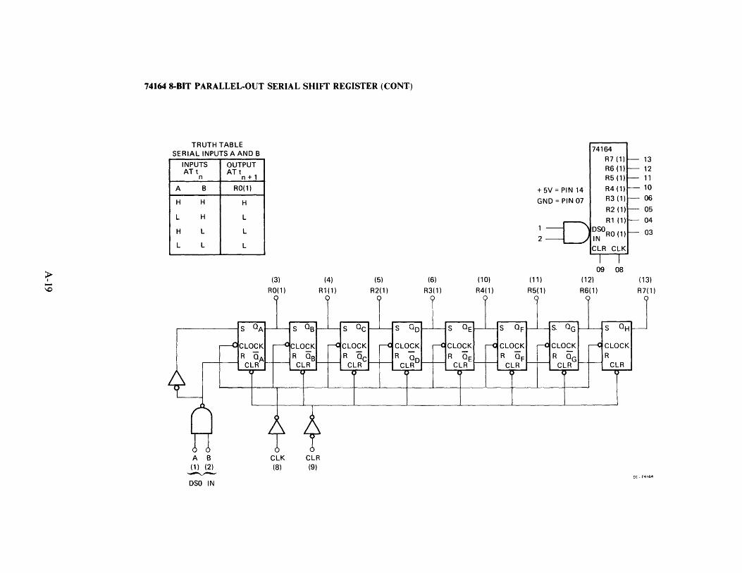
:> I -\0
74164 8-BIT PARALLEL-OUT SERIAL SHIFT REGISTER (CONT)
TRUTH TABLE SERIAL INPUTS A AND B
A
H
L
H
L
INPUTS OUTPUT ATt AT t
n n + 1
B RO(l)
H H
H L
L L
L L
R QA r-----+-------i C L R
A 8 (1) (2) ~
DSO IN
(3)
RO(l)
CLK (8)
(4)
R1(l )
R 0B CLR
CLR (9)
R QC CLR
(5)
R2(1)
CLOCK
R Q CLR
D
(6) (10)
R3(1) R4(1)
74164 R7 (1) R6 (1) R5 (1)
+ 5V = PIN 14 R4 (1)
GND = PIN 07 R3 (1)
R2 (1)
Rl (1) 1 DSORO (1) 2 IN
CLR CLK
09 08 (11 ) (12)
R5(1) R6(1)
CLOCK R
CLR
13 12 11 10
06
05
04
03
(13)
R7(1 )
Ie _74164

74165 PARALLEL-LOAD 8-BIT SHIFT REGISTER
SERIAL (10) INPUT
SH I FT / _(_1 )..-------a LOAD
CLOCK (2)
PARALLEL INPUTS
SERIAL INPUT
6 74165 5 07 4 06
14 04 Rf)(1) 9 COMPLEMENTARY 3 05 }
13 03 7 SERIAL OUTPUTS 12 02 Rf) (f»)
11 D 1 DO
10 SI
LD CLK CI
15
IC-74165A
PARALLEL INPUTS
A-20
D7 (6)
(9) OUTPUT Rf) (1)
(7) OUTPUT Rf) (0)
lC-741658

74174 HEX D-TYPE FLIP-FLOP REGISTER
14 05 R5( 1)
04 R4(1)
03 R3( 1)
6 74174 02 R2(1)
4 01 R 1( 1}
3 DO RO(1)
CLR CLK
9
TRUTH TABLE
INPUT OUTPUT tn tn + 1
0 R( 1)
H H L L
tn = BIT TIME BEFORE CLOCK PU LSE.
tn + 1 = BIT TIME AFTER CLOCK PULSE.
DO (3)
01 (4)
15
12
02 (6)
03 (11)
04 J13)
D5 (14)
CLOCK (9) -
"'"
CLEAR (1 ) -.
PIN (16) = VCC, PIN (8) = GND
A-21
~ RO(1)
,.., ..... CLOCK
CLEAR
9
~ R 1 (1)
,.. CLOCK ~
CLEAR
~
~ R2( 1)
C CLOCK CLEAR .~
~ R3(1)
~ CLOCK CLEAR
'{
( 12) ~ R4(1)
- CLOCK ~
CLEAR
?
(15) r-:---o R5(1)
.... CLOCK " CLEAR
I IC-74174B

74175 QUAD D-TYPE EDGE-TRIGGERED FLIP-FLOP
DATA INPUTS
13 03
12 02
74175 5
01 R 1( 1 ) 7
RHO) 6
DO RO( 1 ) 2
RO(O) 3
ClR ClK
9
TRUTH TABLE INPUT OUTPUTS
tn tn+ 1
0 R(1 )R(O) H H l l l H
tn = Bit time before cloc k pulse.
tn ... 1 = Bit time after clock pulse.
OUTPUTS
(9 ) e L 0 e K 0------1
(1) e lE A R t\..-.----4r'll
(4) RO (2) DO DO (1 )
01 (5) R1 (7) 01 (1 )
R1 elK (0) CLEAR
(12) R2 (10) o 2 n---I----+-_~ 02 (1)
03 (13) R3 03 (1)
Pin (16)= Vce, Pin (S)=GND
Ie -741758
A .. 22

DMCll IPL SYNCHRONOUS LINE UNIT MAINTENANCE MANUAL EK-DMCLU-MM-002
Reader's Comments
Your comments and suggestions will help us in our continuous effort to improve the quality and usefulness of our publications.
What is your general reaction to this manual? In your judgment is it complete, accurate, well organized, well written, etcJ Is ~ easy to us~ ~~~~~~~~~~~~~~~~~~~~~~~~~~~~
What faults or errors have you found in the manual? _~~~~~_~~~_~~_~~~~~_
Does this manual satisfy the need you think it was intended to satisfy? __ ~~~~~_~~_~_
Does it satisfy your needs? ____________ ~ Why? ____________ _
i 0 Please send me the current copy of the Technical Documentation Catalog, which contains information on the remainder of DIGITAL's technical documentation.
Name __ ~ ____ ~~~~~~_~ __ ~ __ Street _~~_~~~~ ___ ~ __ ~_~_
Title City _________________ _
Company_~_~ __ ~~_~_~~~ __ State/Country _____________ _
Department ___ ~~~ _______ _ Zip
Additional copies of this document are available from:
Digital Equipment Corporation 444 Whitney Street Northboro, Ma 01532 Attention: Communications Services (NR2/M15)
Customer Services Section
Order No. ___ E_K_-_D_M_C_L_U_-M_M_-O_O_2 __ _

-----------~~-----------
- - - -- -- -- - - Do Not Tear - Fold Here and Staple - - -- -- -- -- -- -
BUSINESS REPLY MAIL NO POSTAGE STAMP NECESSARY IF MAILED IN THE UNITED STATES
Postage will be paid by:
Digital Equipment Corporation Technical Documentation Department Maynard, Massachusetts 01754
FIRST CLASS PERMIT NO. 33
MAYNARD, MASS.

digital equipment corporation
Pririted in U.S.A.