Embed Size (px)
Citation preview
DM388 Camera Start Kit
User's Guide
Literature Number: SPRUIC7December 2016
2 SPRUIC7–December 2016Submit Documentation Feedback
Copyright © 2016, Texas Instruments Incorporated
Contents
Contents
Preface ........................................................................................................................................ 61 Connecting to DM388 CSK .................................................................................................... 7
1.1 Connecting TMDSCSK388 Module to CSK Carrier Card .............................................................. 8
2 TMDSCSK388 Module ......................................................................................................... 112.1 Key Features................................................................................................................ 122.2 Block Diagram .............................................................................................................. 142.3 Power Supply ............................................................................................................... 16
3 TMDSCSK388 Module Interface Details ................................................................................. 173.1 Clock Distribution........................................................................................................... 183.2 Reset Circuit and Distribution............................................................................................. 193.3 DDR3 Interface ............................................................................................................. 203.4 DDR Timing Control and Software Leveling ............................................................................ 213.5 NAND Flash Interface ..................................................................................................... 223.6 Wi-Fi and BT Interface..................................................................................................... 233.7 Board-to-Board Interface .................................................................................................. 243.8 Boot Mode Configuration .................................................................................................. 253.9 I2C Interface ................................................................................................................. 263.10 I2C Address Mapping ...................................................................................................... 263.11 GPIO Mapping .............................................................................................................. 27
4 TMDSCSK388 Module Physical Specifications ....................................................................... 294.1 Board Layout................................................................................................................ 304.2 Connector Index ............................................................................................................ 31
4.2.1 UFL Connector (J1 and J2) ...................................................................................... 324.2.2 Board-to-Board Male Connector (J3) ........................................................................... 334.2.3 Board-to-Board Male Connector (J4) ........................................................................... 354.2.4 Board-to-Board Termination (J5) ................................................................................ 37
4.3 Switches, Test Points, and LEDs ........................................................................................ 38
5 TMDSCSK388 Power Requirements ...................................................................................... 405.1 Power Distribution .......................................................................................................... 415.2 Power Supply Calculation ................................................................................................. 425.3 Power-up Sequence ....................................................................................................... 43
6 Overview of TMDSCSKCC ................................................................................................... 446.1 Key Features................................................................................................................ 456.2 Block Diagram .............................................................................................................. 466.3 Power Supply ............................................................................................................... 496.4 Overvoltage Protection Circuit ............................................................................................ 50
7 CSK Carrier Card Interface .................................................................................................. 517.1 XDS100 On-Board Emulator Interface .................................................................................. 527.2 Clock Distribution........................................................................................................... 537.3 Reset Circuit and Distribution............................................................................................. 547.4 Camera Interface ........................................................................................................... 557.5 Ethernet Interface .......................................................................................................... 567.6 HDMI and TVOUT Interfaces ............................................................................................. 577.7 LED and Switch Interface ................................................................................................. 57
www.ti.com
3SPRUIC7–December 2016Submit Documentation Feedback
Copyright © 2016, Texas Instruments Incorporated
Contents
7.8 Micro SD Card Interface................................................................................................... 587.9 Audio Codec Interface ..................................................................................................... 587.10 USB Interface ............................................................................................................... 597.11 UART Interface ............................................................................................................. 597.12 I2C Interface ................................................................................................................. 607.13 Connection Between Expansion Connector and CSK Carrier Card................................................. 60
8 CSK Carrier Board Physical Specifications............................................................................ 618.1 Board Layout................................................................................................................ 628.2 Connector Index ............................................................................................................ 64
8.2.1 DC Power Jack (J1)............................................................................................... 678.2.2 Board-to-Board Connector (J3).................................................................................. 678.2.3 Board-to-Board Connector (J4).................................................................................. 698.2.4 Expansion Connector (J15) ...................................................................................... 708.2.5 HDMI Out Type-A Connector (J6)............................................................................... 718.2.6 Camera FPC Connector (J7) .................................................................................... 718.2.7 RJ45 Connector (J8).............................................................................................. 728.2.8 Stereo-Audio Jack (J9 and J10)................................................................................. 728.2.9 Micro USB Connector (J11 and J12) ........................................................................... 738.2.10 Composite Video OUT RCA Connector (J13) ................................................................ 738.2.11 Micro SD Card Connector (J14)................................................................................ 73
8.3 Push Buttons................................................................................................................ 748.4 Test Points .................................................................................................................. 748.5 System LEDs ............................................................................................................... 75
9 CSK Carrier Card Power Requirements ................................................................................. 779.1 Power Distribution .......................................................................................................... 789.2 Power Supply Calculation ................................................................................................. 799.3 Power-up Sequence ....................................................................................................... 80
www.ti.com
4 SPRUIC7–December 2016Submit Documentation Feedback
Copyright © 2016, Texas Instruments Incorporated
List of Figures
List of Figures1-1. Aligned DM388 and CSK Carrier Card ................................................................................... 81-2. DM388 Module Above CSK Carrier Card ................................................................................ 91-3. Connecting DM388 and CSK Carrier Card............................................................................... 91-4. Connected Devices ........................................................................................................ 102-1. TMDSCSK388 Block Diagram............................................................................................ 142-2. TMDSCSK388 Top View .................................................................................................. 152-3. TMDSCSK388 Bottom View .............................................................................................. 153-1. Clock Distribution........................................................................................................... 183-2. Reset Circuit and Distribution............................................................................................. 193-3. DDR3 Bank0 Interface..................................................................................................... 203-4. NAND Flash Interface ..................................................................................................... 223-5. Wi-Fi and BT Interface..................................................................................................... 233-6. Board-to-Board Interface .................................................................................................. 243-7. Boot Mode Configurations ................................................................................................ 253-8. I2C Interface ................................................................................................................. 263-9. GPIO Mapping of LEDs and Switches .................................................................................. 284-1. TMDSCSK388 Assembly Layout (Top View)........................................................................... 304-2. TMDSCSK388 Assembly Layout (Bottom View) ....................................................................... 304-3. TMDSCSK388 Connectors (Top) ........................................................................................ 314-4. TMDSCSK388 Connectors (Bottom) .................................................................................... 324-5. LED, Test Points, and Switches.......................................................................................... 395-1. Power Distribution .......................................................................................................... 415-2. Power Sequencing ......................................................................................................... 436-1. CSK Carrier Card Block Diagram ........................................................................................ 466-2. CSK Carrier Card (Top) ................................................................................................... 476-3. CSK Carrier Card (Bottom) ............................................................................................... 486-4. Overvoltage Protection Circuit ............................................................................................ 507-1. XDS100 On-Board Emulator Interface .................................................................................. 527-2. Clock Distribution........................................................................................................... 537-3. Reset Circuit and Distribution............................................................................................. 547-4. Parallel Camera Interface ................................................................................................. 557-5. Ethernet Interface .......................................................................................................... 567-6. HDMI and TVOUT Interface .............................................................................................. 577-7. Switch and LED Connections............................................................................................. 577-8. Micro SD Card Interface................................................................................................... 587-9. Audio Codec Interface ..................................................................................................... 587-10. USB Interface ............................................................................................................... 597-11. UART Interface ............................................................................................................. 597-12. I2C Interface ................................................................................................................. 607-13. Expansion Connector Interface........................................................................................... 608-1. CSK Carrier Card Assembly Layout (Top) .............................................................................. 628-2. CSK Carrier Card Assembly Layout (Bottom) .......................................................................... 638-3. CSK Carrier Card Connectors (Top)..................................................................................... 658-4. CSK Carrier Card Connectors (Bottom)................................................................................. 668-5. LEDs, Test Points, and Push Buttons on CSK Carrier Card ......................................................... 769-1. CSK Carrier Power Distribution .......................................................................................... 789-2. Power-up Sequence ....................................................................................................... 80
www.ti.com
5SPRUIC7–December 2016Submit Documentation Feedback
Copyright © 2016, Texas Instruments Incorporated
List of Tables
List of Tables2-1. DM388 Power ICs.......................................................................................................... 163-1. Calculated Seed Values ................................................................................................... 213-2. Boot Mode Selection....................................................................................................... 253-3. SW1 Switch Selection ..................................................................................................... 263-4. I2C Address Mapping ...................................................................................................... 263-5. GPIO Mapping .............................................................................................................. 274-1. TMDSCSK388 Module Connectors ...................................................................................... 314-2. UFL Connector J1 and J2................................................................................................. 324-3. Board-to-Board Male Connector (J3) .................................................................................... 334-4. Board-to-Board Male Connector (J4) .................................................................................... 354-5. Board-to-Board Termination (J5) ......................................................................................... 374-6. TMDSCSK388 Module Switch Information ............................................................................. 384-7. TMDSCSK388 Test Points................................................................................................ 385-1. Power Supply Calculations................................................................................................ 426-1. CSK Carrier Card Regulators............................................................................................. 498-1. CSK Carrier Card Connectors ............................................................................................ 648-2. DC Power Jack (J1)........................................................................................................ 678-3. Board-to-Board Connector (J3)........................................................................................... 678-4. Board-to-Board Connector (J4)........................................................................................... 698-5. Expansion Connector (J15) ............................................................................................... 708-6. HDMI Out Type-A Connector (J6) ....................................................................................... 718-7. Camera FPC Connector (J7) ............................................................................................. 718-8. RJ45 Connector (J8)....................................................................................................... 728-9. HP OUT...................................................................................................................... 728-10. MIC IN ....................................................................................................................... 728-11. Micro USB Connector...................................................................................................... 738-12. Composite Video OUT RCA Connector ................................................................................. 738-13. Micro SD Card Connector (J14).......................................................................................... 738-14. CSK Carrier Card Switches ............................................................................................... 748-15. Test Points of CSK Carrier Card ......................................................................................... 748-16. LED Information ............................................................................................................ 759-1. Power Supply Calculation ................................................................................................. 79
6 SPRUIC7–December 2016Submit Documentation Feedback
Copyright © 2016, Texas Instruments Incorporated
About This Manual
PrefaceSPRUIC7–December 2016
About This Manual
This document is for the DM388 processor module.
Related DocumentationInformation regarding the DM388 processor can be found at http://www.ti.com.
Board HistoryPCB Revision HistoryPRDN_REV A Production
AcronymsThe following is a list of acronyms used in this document.
CCS Code Composer Studio™DSP Digital signal processorEEPROM Electrically Erasable Programmable Read-Only MemoryI2C Inter-integrated circuitJTAG Joint test action groupLED Light emitting diodeMMC Multimedia cardUART Universal asynchronous receiver transmitterUSB Universal serial busXDS100 Texas Instruments emulator
TrademarksCode Composer Studio, DaVinci, PowerTune are trademarks of Texas Instruments.ARM, Cortex are registered trademarks of ARM Limited.Skype is a trademark of Skype.
7SPRUIC7–December 2016Submit Documentation Feedback
Copyright © 2016, Texas Instruments Incorporated
Connecting to DM388 CSK
Chapter 1SPRUIC7–December 2016
Connecting to DM388 CSK
Topic ........................................................................................................................... Page
1.1 Connecting TMDSCSK388 Module to CSK Carrier Card ............................................ 8
Connecting TMDSCSK388 Module to CSK Carrier Card www.ti.com
8 SPRUIC7–December 2016Submit Documentation Feedback
Copyright © 2016, Texas Instruments Incorporated
Connecting to DM388 CSK
The DM388 CSK is based on DaVinci™ technology. These digital-media processors are highly integrated,cost-effective, low-power, and have programmable platforms that leverage TI’s DaVinci processortechnology to meet the processing requirements of HD video conferencing, Skype™ endpoints, IPnetcam, digital signage, media players and adapters, mobile medical imaging, network projectors, homeaudio and video equipment, and similar devices in SD, HD, and 4K × 2K resolutions.
The DM388 camera starter kit is a development platform with the DM388 processor module connected toa CSK carrier card over board-to-board connectors. Features of the DM388 module and CSK carrier cardare detailed in the subsections that follow.
DM388 camera starter kit contents:• TMDSCSK388 module• CSK carrier card• Camera module (LI-CAM-AR0331-324-1.8) with FPC cable
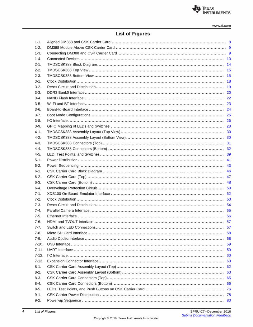
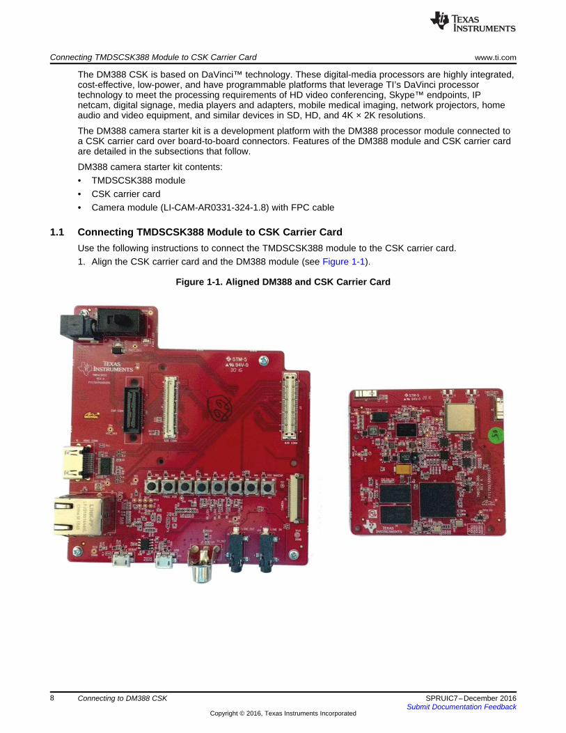
1.1 Connecting TMDSCSK388 Module to CSK Carrier CardUse the following instructions to connect the TMDSCSK388 module to the CSK carrier card.1. Align the CSK carrier card and the DM388 module (see Figure 1-1).
Figure 1-1. Aligned DM388 and CSK Carrier Card
www.ti.com Connecting TMDSCSK388 Module to CSK Carrier Card
9SPRUIC7–December 2016Submit Documentation Feedback
Copyright © 2016, Texas Instruments Incorporated
Connecting to DM388 CSK
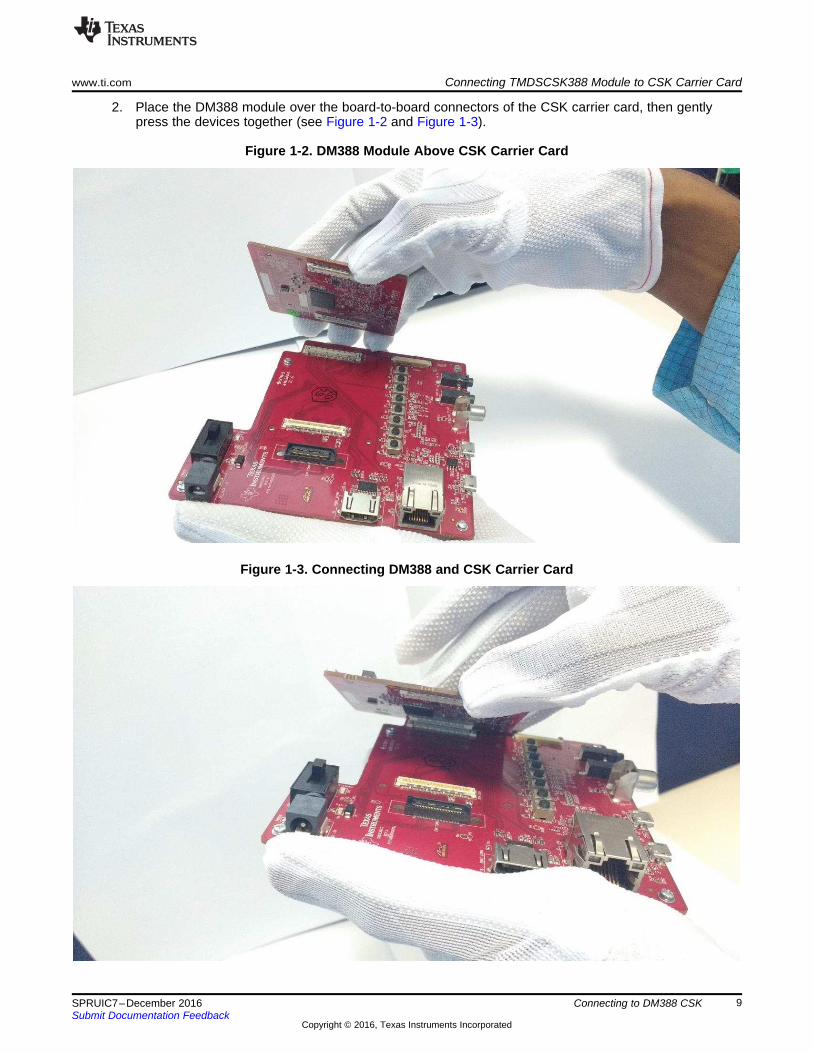
2. Place the DM388 module over the board-to-board connectors of the CSK carrier card, then gentlypress the devices together (see Figure 1-2 and Figure 1-3).
Figure 1-2. DM388 Module Above CSK Carrier Card
Figure 1-3. Connecting DM388 and CSK Carrier Card
Connecting TMDSCSK388 Module to CSK Carrier Card www.ti.com
10 SPRUIC7–December 2016Submit Documentation Feedback
Copyright © 2016, Texas Instruments Incorporated
Connecting to DM388 CSK
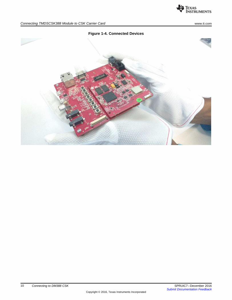
Figure 1-4. Connected Devices
11SPRUIC7–December 2016Submit Documentation Feedback
Copyright © 2016, Texas Instruments Incorporated
TMDSCSK388 Module
Chapter 2SPRUIC7–December 2016
TMDSCSK388 Module
Topic ........................................................................................................................... Page
2.1 Key Features ..................................................................................................... 122.2 Block Diagram ................................................................................................... 142.3 Power Supply .................................................................................................... 16
Key Features www.ti.com
12 SPRUIC7–December 2016Submit Documentation Feedback
Copyright © 2016, Texas Instruments Incorporated
TMDSCSK388 Module
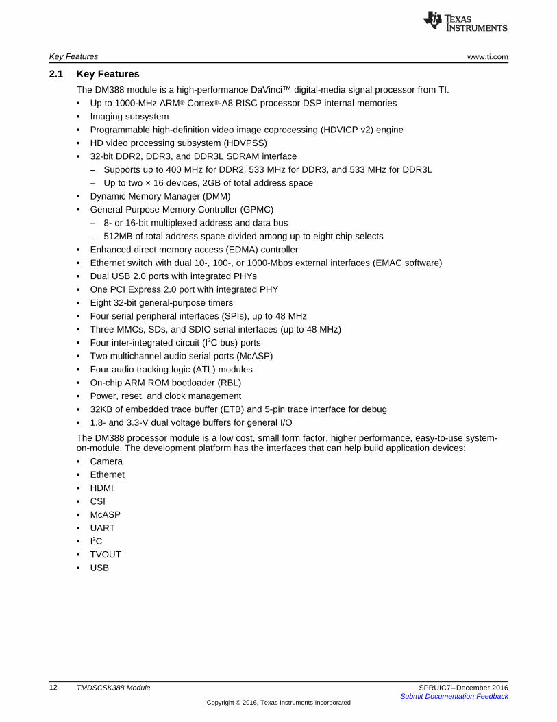
2.1 Key FeaturesThe DM388 module is a high-performance DaVinci™ digital-media signal processor from TI.• Up to 1000-MHz ARM® Cortex®-A8 RISC processor DSP internal memories• Imaging subsystem• Programmable high-definition video image coprocessing (HDVICP v2) engine• HD video processing subsystem (HDVPSS)• 32-bit DDR2, DDR3, and DDR3L SDRAM interface
– Supports up to 400 MHz for DDR2, 533 MHz for DDR3, and 533 MHz for DDR3L– Up to two × 16 devices, 2GB of total address space
• Dynamic Memory Manager (DMM)• General-Purpose Memory Controller (GPMC)
– 8- or 16-bit multiplexed address and data bus– 512MB of total address space divided among up to eight chip selects
• Enhanced direct memory access (EDMA) controller• Ethernet switch with dual 10-, 100-, or 1000-Mbps external interfaces (EMAC software)• Dual USB 2.0 ports with integrated PHYs• One PCI Express 2.0 port with integrated PHY• Eight 32-bit general-purpose timers• Four serial peripheral interfaces (SPIs), up to 48 MHz• Three MMCs, SDs, and SDIO serial interfaces (up to 48 MHz)• Four inter-integrated circuit (I2C bus) ports• Two multichannel audio serial ports (McASP)• Four audio tracking logic (ATL) modules• On-chip ARM ROM bootloader (RBL)• Power, reset, and clock management• 32KB of embedded trace buffer (ETB) and 5-pin trace interface for debug• 1.8- and 3.3-V dual voltage buffers for general I/O
The DM388 processor module is a low cost, small form factor, higher performance, easy-to-use system-on-module. The development platform has the interfaces that can help build application devices:• Camera• Ethernet• HDMI• CSI• McASP• UART• I2C• TVOUT• USB
www.ti.com Key Features
13SPRUIC7–December 2016Submit Documentation Feedback
Copyright © 2016, Texas Instruments Incorporated
TMDSCSK388 Module
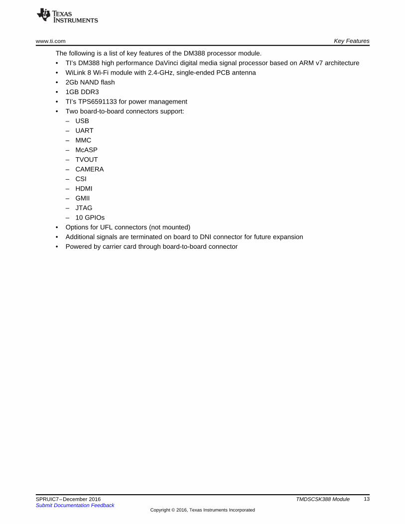
The following is a list of key features of the DM388 processor module.• TI’s DM388 high performance DaVinci digital media signal processor based on ARM v7 architecture• WiLink 8 Wi-Fi module with 2.4-GHz, single-ended PCB antenna• 2Gb NAND flash• 1GB DDR3• TI’s TPS6591133 for power management• Two board-to-board connectors support:
– USB– UART– MMC– McASP– TVOUT– CAMERA– CSI– HDMI– GMII– JTAG– 10 GPIOs
• Options for UFL connectors (not mounted)• Additional signals are terminated on board to DNI connector for future expansion• Powered by carrier card through board-to-board connector
DM388
DDR CORE SUPPLY
DDR0
GPMC
DEVOSC_MXI
DEVOSC_MXOAUXOSC_MXI
AUXOSC_MXO
CLKIN32
JTAG
RESET OUT
PORn
HD DAC SUPPLY CORE SUPPLY
I2C0
TVOUTEMAC0
USB0.1
UART0, 1, 2MMC1HDMI
I2C 2,3SPI0, 1
McASP1CS12CAM
GPIOs3V3 I/O SUPPLY
MMC0, McASP0,UART2
HDDAC VIN McASP0McASP1
MMC2 PCIe UART0UART2 Wi-Fi Module
WL1837
LevelTranslators
Board-to-Board Termination
DDR PowerTPS51216
2 x 4 GbDDR3 X 16
MT41K256M16TW
2 GbNAND Flash
MT29F2G16ABAEAWP:E
Boa
rd-t
o-B
oard
Con
nect
orB
oard-to-Board C
onnector
LDOTPS71711DCKR
PMICTPS6591133
DELAYED 3.3
5 V, 3.3
PWRON
3.3 V
RESET IN
nRESPWRON2DDR PGOOD
20 MHZ
27 MHZ
32.768 KHz OSC
MUXERCAM / UART2
UART2RTS &CTS
CAM CLK& FLD
1.1 V
SPI1
CHIP ANTENNA5 V
Copyright © 2016, Texas Instruments Incorporated
Block Diagram www.ti.com
14 SPRUIC7–December 2016Submit Documentation Feedback
Copyright © 2016, Texas Instruments Incorporated
TMDSCSK388 Module
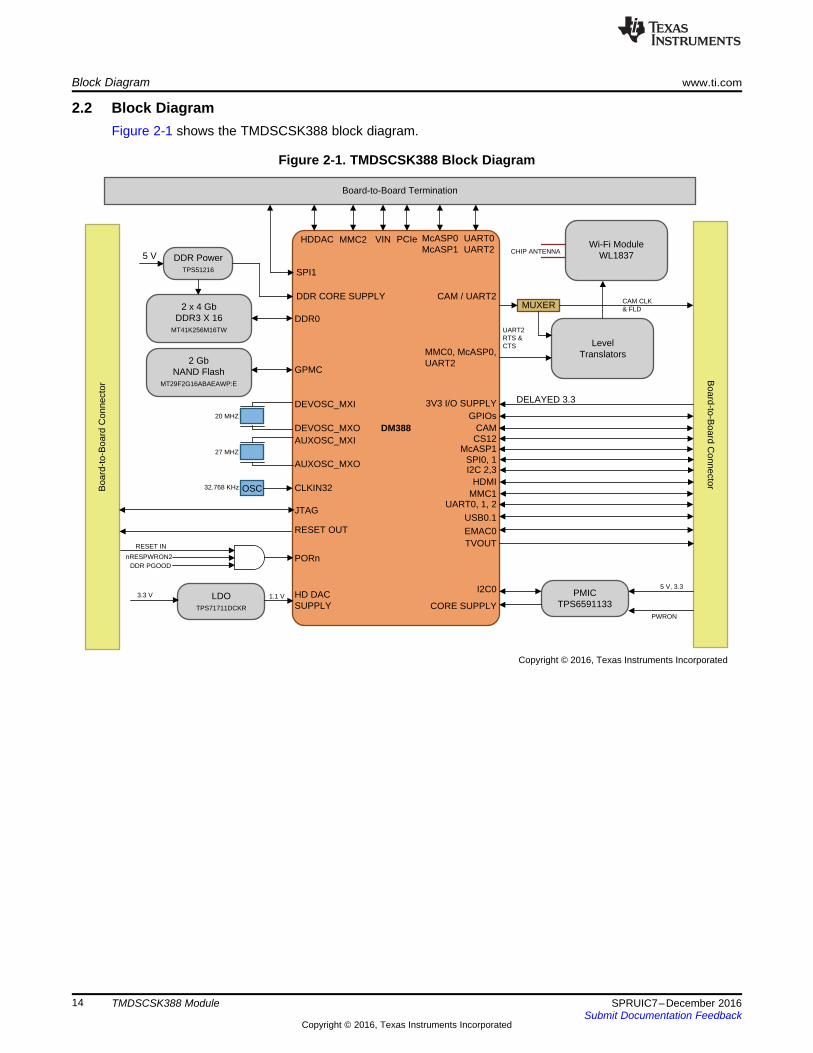
2.2 Block DiagramFigure 2-1 shows the TMDSCSK388 block diagram.
Figure 2-1. TMDSCSK388 Block Diagram
www.ti.com Block Diagram
15SPRUIC7–December 2016Submit Documentation Feedback
Copyright © 2016, Texas Instruments Incorporated
TMDSCSK388 Module
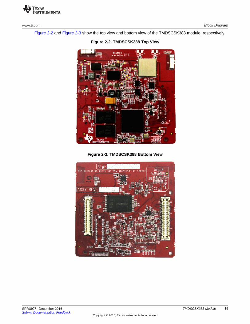
Figure 2-2 and Figure 2-3 show the top view and bottom view of the TMDSCSK388 module, respectively.
Figure 2-2. TMDSCSK388 Top View
Figure 2-3. TMDSCSK388 Bottom View
Power Supply www.ti.com
16 SPRUIC7–December 2016Submit Documentation Feedback
Copyright © 2016, Texas Instruments Incorporated
TMDSCSK388 Module
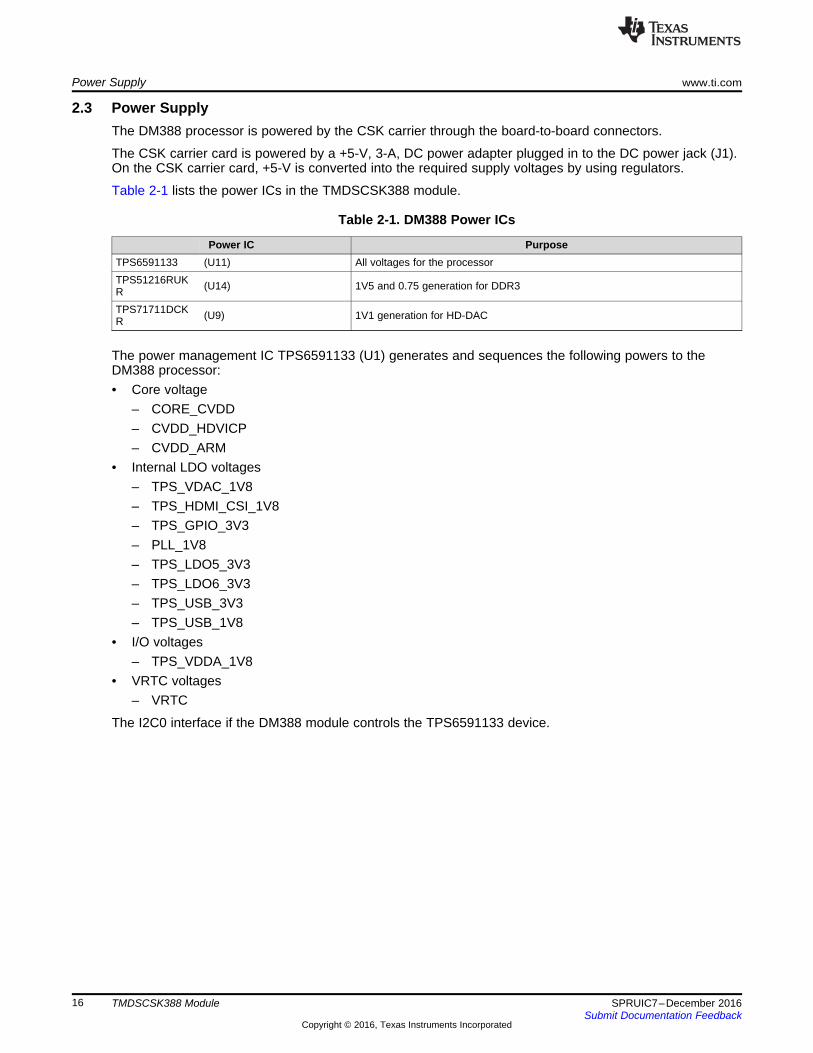
2.3 Power SupplyThe DM388 processor is powered by the CSK carrier through the board-to-board connectors.
The CSK carrier card is powered by a +5-V, 3-A, DC power adapter plugged in to the DC power jack (J1).On the CSK carrier card, +5-V is converted into the required supply voltages by using regulators.
Table 2-1 lists the power ICs in the TMDSCSK388 module.
Table 2-1. DM388 Power ICs
Power IC PurposeTPS6591133 (U11) All voltages for the processorTPS51216RUKR (U14) 1V5 and 0.75 generation for DDR3
TPS71711DCKR (U9) 1V1 generation for HD-DAC
The power management IC TPS6591133 (U1) generates and sequences the following powers to theDM388 processor:• Core voltage
– CORE_CVDD– CVDD_HDVICP– CVDD_ARM
• Internal LDO voltages– TPS_VDAC_1V8– TPS_HDMI_CSI_1V8– TPS_GPIO_3V3– PLL_1V8– TPS_LDO5_3V3– TPS_LDO6_3V3– TPS_USB_3V3– TPS_USB_1V8
• I/O voltages– TPS_VDDA_1V8
• VRTC voltages– VRTC
The I2C0 interface if the DM388 module controls the TPS6591133 device.
17SPRUIC7–December 2016Submit Documentation Feedback
Copyright © 2016, Texas Instruments Incorporated
TMDSCSK388 Module Interface Details
Chapter 3SPRUIC7–December 2016
TMDSCSK388 Module Interface Details
Topic ........................................................................................................................... Page
3.1 Clock Distribution .............................................................................................. 183.2 Reset Circuit and Distribution.............................................................................. 193.3 DDR3 Interface................................................................................................... 203.4 DDR Timing Control and Software Leveling........................................................... 213.5 NAND Flash Interface ......................................................................................... 223.6 Wi-Fi and BT Interface ........................................................................................ 233.7 Board-to-Board Interface..................................................................................... 243.8 Boot Mode Configuration .................................................................................... 253.9 I2C Interface ....................................................................................................... 263.10 I2C Address Mapping .......................................................................................... 263.11 GPIO Mapping.................................................................................................... 27
32.768 KHz
DM388 Processor
Board-to-B
oard Connector
WiLinkTM 8WL1837MOD
PMICTPS6591133
20 MHz 27 MHzDNI
CLK32OUT_PMIC EXT_32CLK
DEVOSCMXI
DEVOSCMXO
AUXMXI
AUXMXO CLKOUT1
McASP1_AHCLKx
EMAC[0]_GMTCLK
MDIO_CLK
JTAG_TCKMMC1_CLK
CAM_PCLK
CLKIN32
Copyright © 2016, Texas Instruments Incorporated
Clock Distribution www.ti.com
18 SPRUIC7–December 2016Submit Documentation Feedback
Copyright © 2016, Texas Instruments Incorporated
TMDSCSK388 Module Interface Details
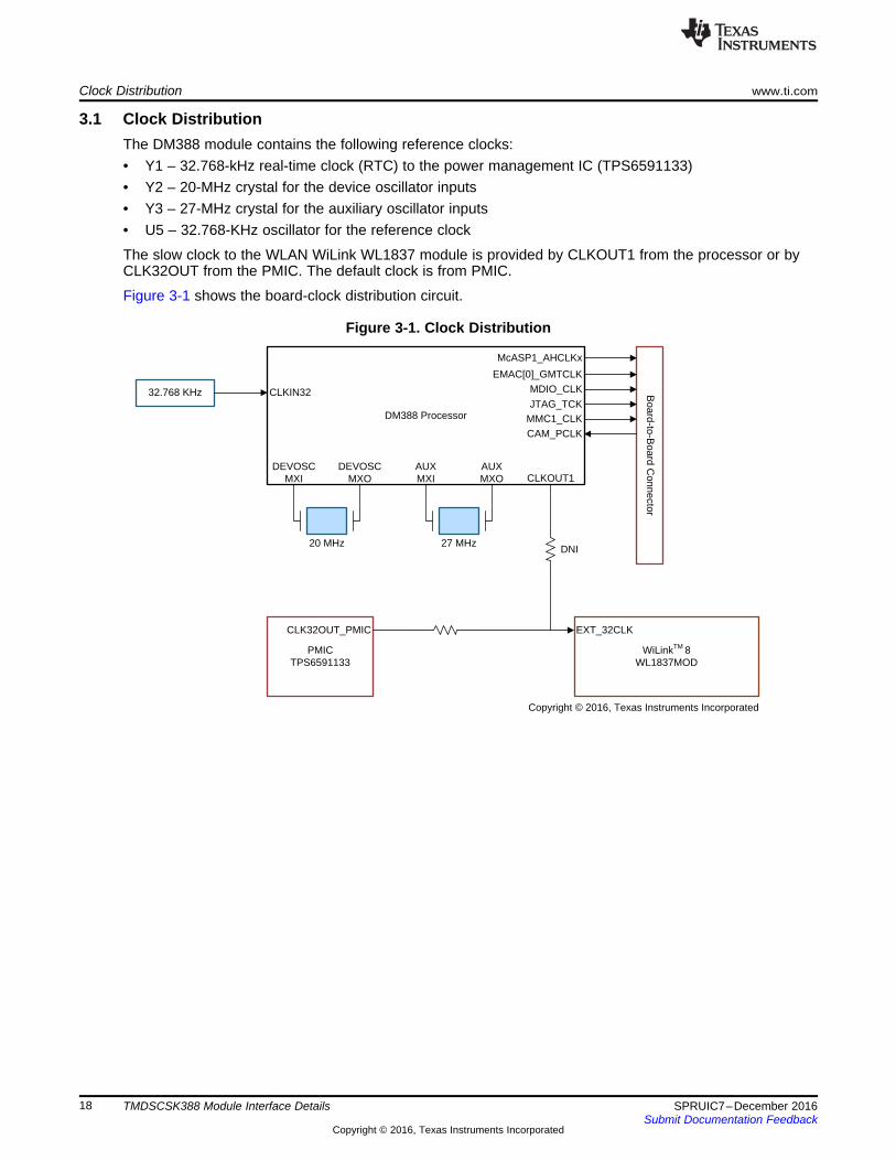
3.1 Clock DistributionThe DM388 module contains the following reference clocks:• Y1 – 32.768-kHz real-time clock (RTC) to the power management IC (TPS6591133)• Y2 – 20-MHz crystal for the device oscillator inputs• Y3 – 27-MHz crystal for the auxiliary oscillator inputs• U5 – 32.768-KHz oscillator for the reference clock
The slow clock to the WLAN WiLink WL1837 module is provided by CLKOUT1 from the processor or byCLK32OUT from the PMIC. The default clock is from PMIC.
Figure 3-1 shows the board-clock distribution circuit.
Figure 3-1. Clock Distribution
DM388 Processor
Ethernet Reset
Camera Reset
Warm Reset
Board-to-Board Connector
BB_PORn from CCA
ND
DDR Power ICTPS51216
PMICTPS6591133
DDR_PGOOD
nRESPWRON2
10 K
10 K 10 K 10 K
3.3 V
PORn
RESETn
RESETOUTn
CAM_RESET
GP[3]_20
Copyright © 2016, Texas Instruments Incorporated
www.ti.com Reset Circuit and Distribution
19SPRUIC7–December 2016Submit Documentation Feedback
Copyright © 2016, Texas Instruments Incorporated
TMDSCSK388 Module Interface Details
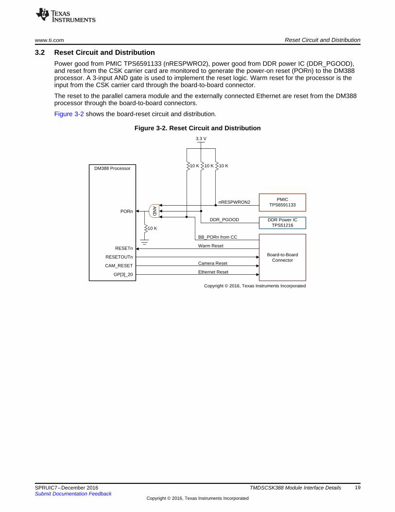
3.2 Reset Circuit and DistributionPower good from PMIC TPS6591133 (nRESPWRO2), power good from DDR power IC (DDR_PGOOD),and reset from the CSK carrier card are monitored to generate the power-on reset (PORn) to the DM388processor. A 3-input AND gate is used to implement the reset logic. Warm reset for the processor is theinput from the CSK carrier card through the board-to-board connector.
The reset to the parallel camera module and the externally connected Ethernet are reset from the DM388processor through the board-to-board connectors.
Figure 3-2 shows the board-reset circuit and distribution.
Figure 3-2. Reset Circuit and Distribution
DM388 Processor
DDR3MT41K256M16TW
DDR3MT41K256M16TW
DDR0_DQ[0:15]
DDR0_DQS[0:1]
DDR0_DQSn[0:1]
DDR0_DQM[0:1]
DDR0_DQ[16:31]
DDR0_DQS[2:3]
DDR0_DQSn[2:3]
DDR0_DQM[2:3]
DDR0_CLKn
DDR0_CLK
DDR0_BA[0:2]
DDR0_A[0:14]
DDR0_CASn
DDR0_WEn
DDR0_CS0n
DDR0_CLKe
DDR0_RST
DDR0_RASn
DDR0_ODT
1.5 V
DVDD_DDR
Copyright © 2016, Texas Instruments Incorporated
DDR3 Interface www.ti.com
20 SPRUIC7–December 2016Submit Documentation Feedback
Copyright © 2016, Texas Instruments Incorporated
TMDSCSK388 Module Interface Details
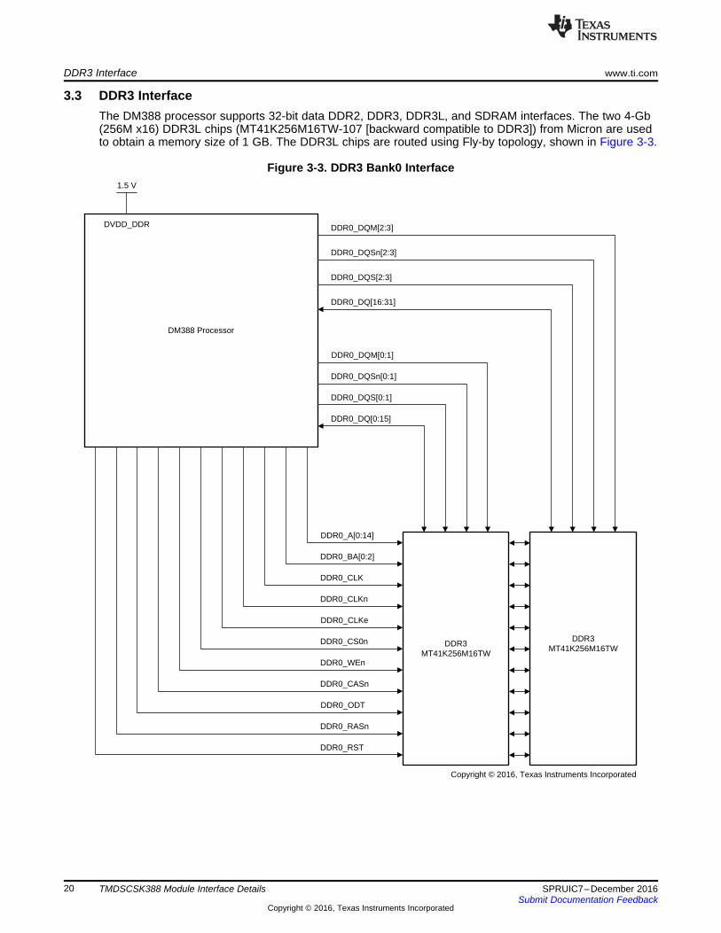
3.3 DDR3 InterfaceThe DM388 processor supports 32-bit data DDR2, DDR3, DDR3L, and SDRAM interfaces. The two 4-Gb(256M x16) DDR3L chips (MT41K256M16TW-107 [backward compatible to DDR3]) from Micron are usedto obtain a memory size of 1 GB. The DDR3L chips are routed using Fly-by topology, shown in Figure 3-3.
Figure 3-3. DDR3 Bank0 Interface
www.ti.com DDR Timing Control and Software Leveling
21SPRUIC7–December 2016Submit Documentation Feedback
Copyright © 2016, Texas Instruments Incorporated
TMDSCSK388 Module Interface Details
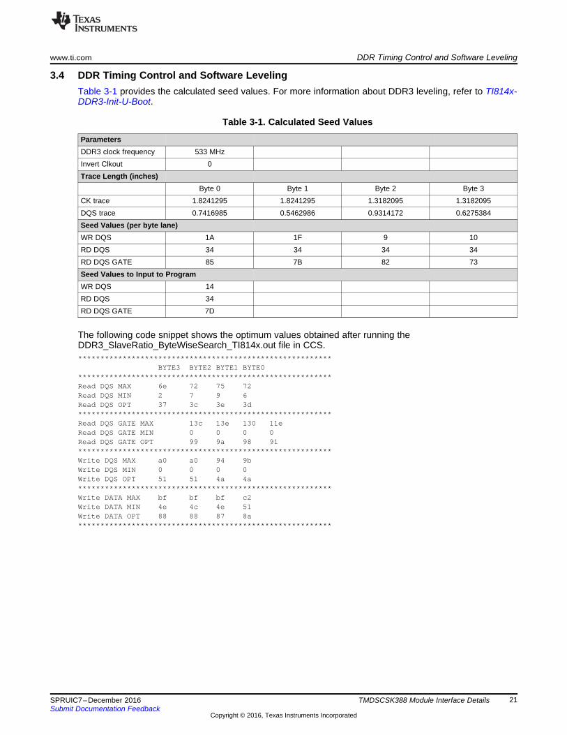
3.4 DDR Timing Control and Software LevelingTable 3-1 provides the calculated seed values. For more information about DDR3 leveling, refer to TI814x-DDR3-Init-U-Boot.
Table 3-1. Calculated Seed Values
ParametersDDR3 clock frequency 533 MHzInvert Clkout 0Trace Length (inches)
Byte 0 Byte 1 Byte 2 Byte 3CK trace 1.8241295 1.8241295 1.3182095 1.3182095DQS trace 0.7416985 0.5462986 0.9314172 0.6275384Seed Values (per byte lane)WR DQS 1A 1F 9 10RD DQS 34 34 34 34RD DQS GATE 85 7B 82 73Seed Values to Input to ProgramWR DQS 14RD DQS 34RD DQS GATE 7D
The following code snippet shows the optimum values obtained after running theDDR3_SlaveRatio_ByteWiseSearch_TI814x.out file in CCS.*********************************************************
BYTE3 BYTE2 BYTE1 BYTE0*********************************************************Read DQS MAX 6e 72 75 72Read DQS MIN 2 7 9 6Read DQS OPT 37 3c 3e 3d*********************************************************Read DQS GATE MAX 13c 13e 130 11eRead DQS GATE MIN 0 0 0 0Read DQS GATE OPT 99 9a 98 91*********************************************************Write DQS MAX a0 a0 94 9bWrite DQS MIN 0 0 0 0Write DQS OPT 51 51 4a 4a*********************************************************Write DATA MAX bf bf bf c2Write DATA MIN 4e 4c 4e 51Write DATA OPT 88 88 87 8a*********************************************************
3.3 V
DM388 Processor
NAND FlashMT29F2G16ABAEAWP:E
CEn
REn
WEn
ALE
CLE
I/O[0:15]
WPn
#RB
GPMC_CS0n
GPMC_Oen_REn
WEn
ALE
CLE
I/O[0:15]
WPn
#RB
3.3 V
Copyright © 2016, Texas Instruments Incorporated
NAND Flash Interface www.ti.com
22 SPRUIC7–December 2016Submit Documentation Feedback
Copyright © 2016, Texas Instruments Incorporated
TMDSCSK388 Module Interface Details
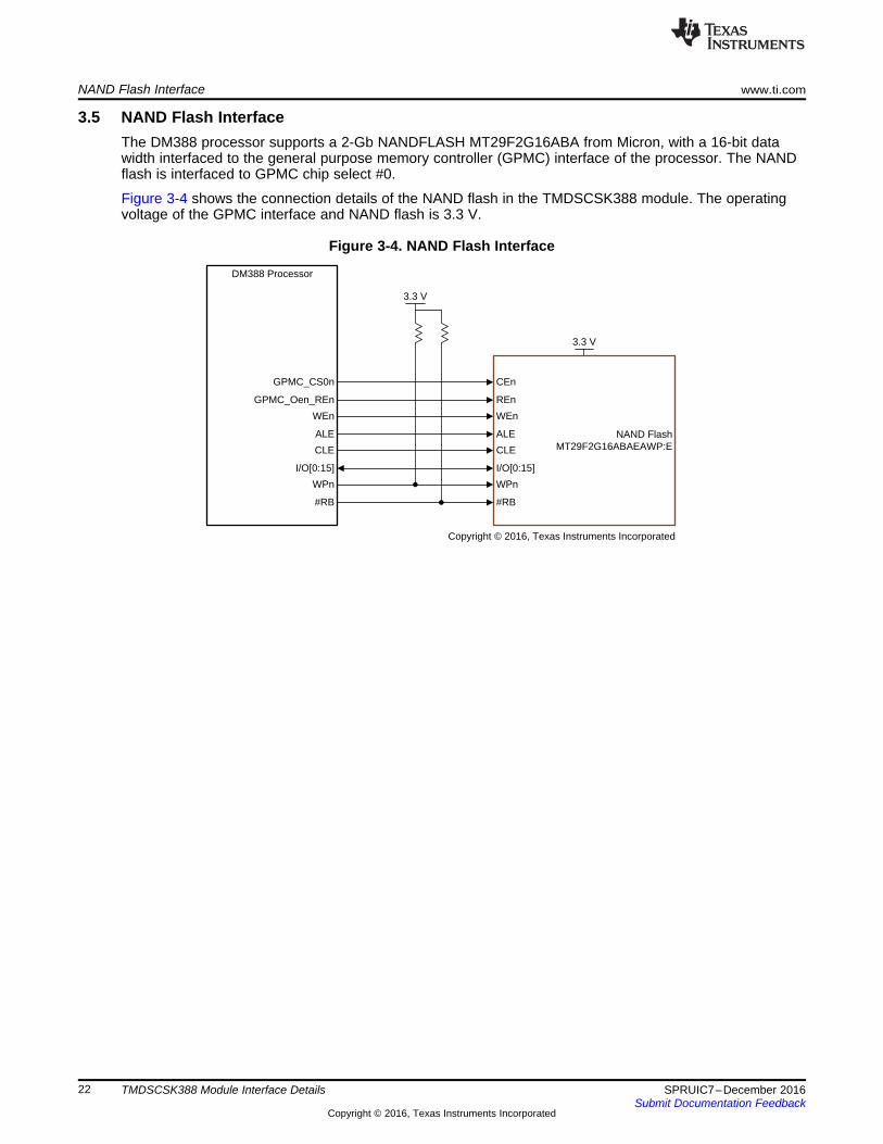
3.5 NAND Flash InterfaceThe DM388 processor supports a 2-Gb NANDFLASH MT29F2G16ABA from Micron, with a 16-bit datawidth interfaced to the general purpose memory controller (GPMC) interface of the processor. The NANDflash is interfaced to GPMC chip select #0.
Figure 3-4 shows the connection details of the NAND flash in the TMDSCSK388 module. The operatingvoltage of the GPMC interface and NAND flash is 3.3 V.
Figure 3-4. NAND Flash Interface
DM388 Processor
Voltage Level Translator
TXS0108ERGYR
Voltage Level Translator (x3)
SN74AVC4T245
WiLinkTM 8 Wi-Fi Module
WL1837MOD
MMC0_DAT[0:3]
MMC0_CLK
MMC0_CMD
1.8 V3.3 V
3.3 V 1.8 V 3.3 V 1.8 V
UART2_TXD
UART2_RXD
BT_EN
WLAN_EN
WLAN_IRQ
WLAN_CLOCKOUT1
McASP0_AXR1
McASP0_AXR0
McASP0_AFSX
McASP0_ACLKX
WL_SDIO
BT_HCI
EN, CLK, IRQ
EXT_32K
BT_AUD
VBAT VIO
RF_ANT1
RF_ANT2
UART3
EN, CLK, IRQ
McASP0
MuxerSN74CBTLV3257RGYR
UART2_TXD
UART2_RXD
CAM_FLD
CAM_PCLK
(To Board-to-Board Connector)
UA
RT
2_R
TS
n
UA
RT
2_C
TS
n
Copyright © 2016, Texas Instruments Incorporated
www.ti.com Wi-Fi and BT Interface
23SPRUIC7–December 2016Submit Documentation Feedback
Copyright © 2016, Texas Instruments Incorporated
TMDSCSK388 Module Interface Details
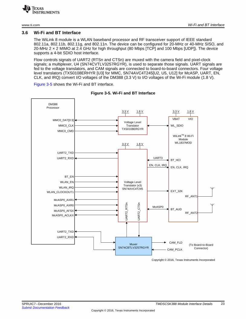
3.6 Wi-Fi and BT InterfaceThe WiLink 8 module is a WLAN baseband processor and RF transceiver support of IEEE standard802.11a, 802.11b, 802.11g, and 802.11n. The device can be configured for 20-MHz or 40-MHz SISO, and20-MHz 2 × 2 MIMO at 2.4 GHz for high throughput (80 Mbps [TCP] and 100 Mbps [UDP]). The devicesupports a 4-bit SDIO host interface.
Flow controls signals of UART2 (RTSn and CTSn) are muxed with the camera field and pixel-clocksignals; a multiplexer, U4 (SN74CVTLV3257RGYR), is used to separate those signals. UART signals arefed to the voltage translators, and CAM signals are connected to board-to-board connectors. Four voltagelevel translators (TXS0108ERHYR [U3] for MMC, SN74AVC4T245[U2, U5, U12] for McASP, UART, EN,CLK, and IRQ) convert I/O voltages of the DM388 (3.3 V) to I/O voltages of the Wi-Fi module (1.8 V).
Figure 3-5 shows the Wi-Fi and BT interface.
Figure 3-5. Wi-Fi and BT Interface
Boa
rd-t
o-B
oard
Con
nect
or
DM388 Processor
USB1
UART0
MMC1
McASP1
SPIO
USB0
JTAG
Board-to-B
oard Connector
Board-to-Board Termination
UA
RT
VIN
PC
Ie
MM
C2
McA
SP
HDMI
UART1
RESET OUT
TVOUT
CAM
EMAC0
GPIOs
I2Cs
CSI
3V3 Enable
VCC_5V0
VCC_3V3
PMIC_3V3
1V8
VCC_CAM
Copyright © 2016, Texas Instruments Incorporated
Board-to-Board Interface www.ti.com
24 SPRUIC7–December 2016Submit Documentation Feedback
Copyright © 2016, Texas Instruments Incorporated
TMDSCSK388 Module Interface Details
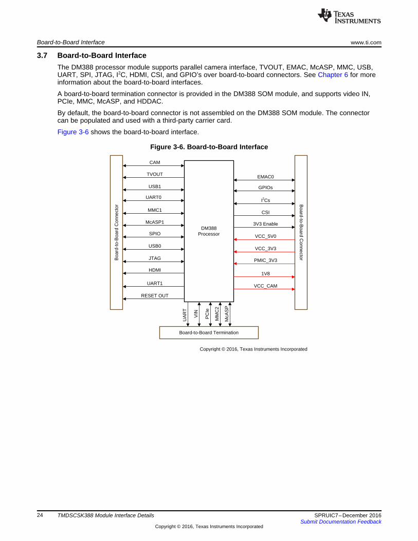
3.7 Board-to-Board InterfaceThe DM388 processor module supports parallel camera interface, TVOUT, EMAC, McASP, MMC, USB,UART, SPI, JTAG, I2C, HDMI, CSI, and GPIO’s over board-to-board connectors. See Chapter 6 for moreinformation about the board-to-board interfaces.
A board-to-board termination connector is provided in the DM388 SOM module, and supports video IN,PCIe, MMC, McASP, and HDDAC.
By default, the board-to-board connector is not assembled on the DM388 SOM module. The connectorcan be populated and used with a third-party carrier card.
Figure 3-6 shows the board-to-board interface.
Figure 3-6. Board-to-Board Interface
www.ti.com Boot Mode Configuration
25SPRUIC7–December 2016Submit Documentation Feedback
Copyright © 2016, Texas Instruments Incorporated
TMDSCSK388 Module Interface Details
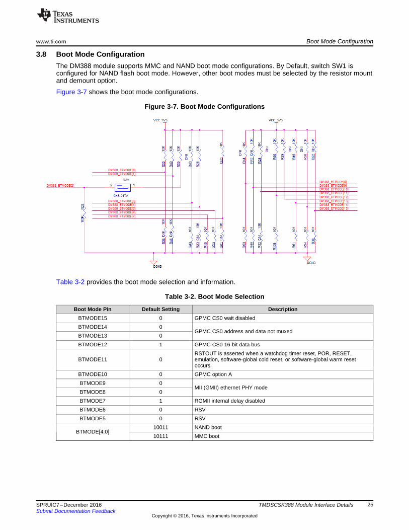
3.8 Boot Mode ConfigurationThe DM388 module supports MMC and NAND boot mode configurations. By Default, switch SW1 isconfigured for NAND flash boot mode. However, other boot modes must be selected by the resistor mountand demount option.
Figure 3-7 shows the boot mode configurations.
Figure 3-7. Boot Mode Configurations
Table 3-2 provides the boot mode selection and information.
Table 3-2. Boot Mode Selection
Boot Mode Pin Default Setting DescriptionBTMODE15 0 GPMC CS0 wait disabledBTMODE14 0
GPMC CS0 address and data not muxedBTMODE13 0BTMODE12 1 GPMC CS0 16-bit data bus
BTMODE11 0RSTOUT is asserted when a watchdog timer reset, POR, RESET,emulation, software-global cold reset, or software-global warm resetoccurs
BTMODE10 0 GPMC option ABTMODE9 0
MII (GMII) ethernet PHY modeBTMODE8 0BTMODE7 1 RGMII internal delay disabledBTMODE6 0 RSVBTMODE5 0 RSV
BTMODE[4:0]10011 NAND boot10111 MMC boot
DM388Processor
PMICTPS6591133
EP Red
I2C0_SCL
I2C0_SDA
HDMI_SCL
HDMI_SDA
I2C2_SCL
I2C2_SDA
Copyright © 2016, Texas Instruments Incorporated
I2C Interface www.ti.com
26 SPRUIC7–December 2016Submit Documentation Feedback
Copyright © 2016, Texas Instruments Incorporated
TMDSCSK388 Module Interface Details
Table 3-3 provides the SW1 switch-selection information.
Table 3-3. SW1 Switch Selection
SW1 SelectionON MMC bootOFF NAND
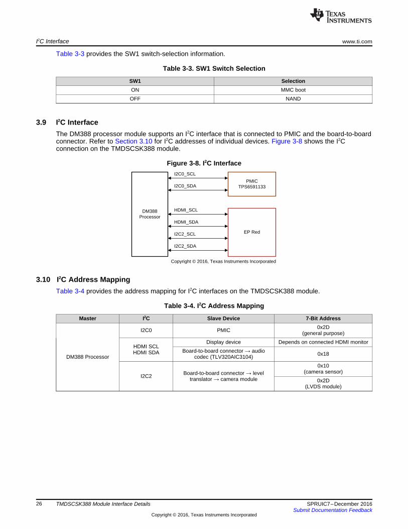
3.9 I2C InterfaceThe DM388 processor module supports an I2C interface that is connected to PMIC and the board-to-boardconnector. Refer to Section 3.10 for I2C addresses of individual devices. Figure 3-8 shows the I2Cconnection on the TMDSCSK388 module.
Figure 3-8. I2C Interface
3.10 I2C Address MappingTable 3-4 provides the address mapping for I2C interfaces on the TMDSCSK388 module.
Table 3-4. I2C Address Mapping
Master I2C Slave Device 7-Bit Address
DM388 Processor
I2C0 PMIC 0x2D(general purpose)
HDMI SCLHDMI SDA
Display device Depends on connected HDMI monitorBoard-to-board connector → audio
codec (TLV320AIC3104) 0x18
I2C2 Board-to-board connector → leveltranslator → camera module
0x10(camera sensor)
0x2D(LVDS module)
www.ti.com GPIO Mapping
27SPRUIC7–December 2016Submit Documentation Feedback
Copyright © 2016, Texas Instruments Incorporated
TMDSCSK388 Module Interface Details
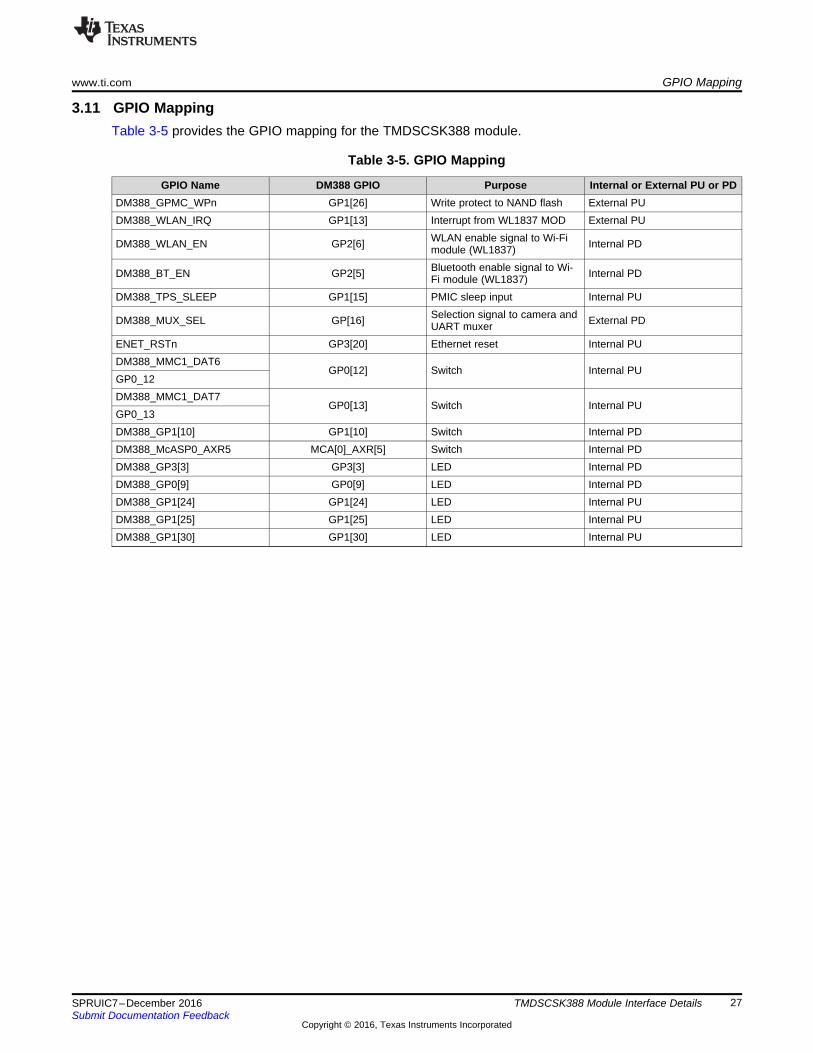
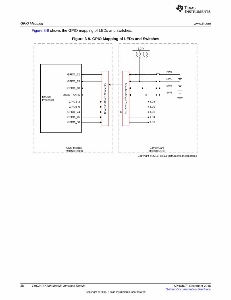
3.11 GPIO MappingTable 3-5 provides the GPIO mapping for the TMDSCSK388 module.
Table 3-5. GPIO Mapping
GPIO Name DM388 GPIO Purpose Internal or External PU or PDDM388_GPMC_WPn GP1[26] Write protect to NAND flash External PUDM388_WLAN_IRQ GP1[13] Interrupt from WL1837 MOD External PU
DM388_WLAN_EN GP2[6] WLAN enable signal to Wi-Fimodule (WL1837) Internal PD
DM388_BT_EN GP2[5] Bluetooth enable signal to Wi-Fi module (WL1837) Internal PD
DM388_TPS_SLEEP GP1[15] PMIC sleep input Internal PU
DM388_MUX_SEL GP[16] Selection signal to camera andUART muxer External PD
ENET_RSTn GP3[20] Ethernet reset Internal PUDM388_MMC1_DAT6
GP0[12] Switch Internal PUGP0_12DM388_MMC1_DAT7
GP0[13] Switch Internal PUGP0_13DM388_GP1[10] GP1[10] Switch Internal PDDM388_McASP0_AXR5 MCA[0]_AXR[5] Switch Internal PDDM388_GP3[3] GP3[3] LED Internal PDDM388_GP0[9] GP0[9] LED Internal PDDM388_GP1[24] GP1[24] LED Internal PUDM388_GP1[25] GP1[25] LED Internal PUDM388_GP1[30] GP1[30] LED Internal PU
Boa
rd-t
o-B
oard
Con
nect
orB
oard-to-Board C
onnector
SOM ModuleTMDSCSK388
Carrier CardTMDSCSKCC
DM388 Processor
GPIO0_12
GPIO0_13
GPIO1_10
McASP_AXR5
GPIO3_3
GPIO0_9
GPIO1_24
GPIO1_25
LD6
GPIO1_30
LD5
LD8
LD4
LD7
SW7
SW6
SW5
SW8
3.3 V
Copyright © 2016, Texas Instruments Incorporated
GPIO Mapping www.ti.com
28 SPRUIC7–December 2016Submit Documentation Feedback
Copyright © 2016, Texas Instruments Incorporated
TMDSCSK388 Module Interface Details
Figure 3-9 shows the GPIO mapping of LEDs and switches.
Figure 3-9. GPIO Mapping of LEDs and Switches
29SPRUIC7–December 2016Submit Documentation Feedback
Copyright © 2016, Texas Instruments Incorporated
TMDSCSK388 Module Physical Specifications
Chapter 4SPRUIC7–December 2016
TMDSCSK388 Module Physical Specifications
Topic ........................................................................................................................... Page
4.1 Board Layout ..................................................................................................... 304.2 Connector Index................................................................................................. 31
4.2.1 UFL Connector (J1 and J2) ........................................................................... 324.2.2 Board-to-Board Male Connector (J3) ................................................................ 334.2.3 Board-to-Board Male Connector (J4) ................................................................ 354.2.4 Board-to-Board Termination (J5) ..................................................................... 37
4.3 Switches, Test Points, and LEDs.......................................................................... 38
Board Layout www.ti.com
30 SPRUIC7–December 2016Submit Documentation Feedback
Copyright © 2016, Texas Instruments Incorporated
TMDSCSK388 Module Physical Specifications
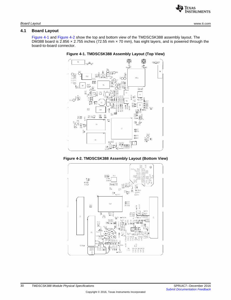
4.1 Board LayoutFigure 4-1 and Figure 4-2 show the top and bottom view of the TMDSCSK388 assembly layout. TheDM388 board is 2.856 × 2.755 inches (72.55 mm × 70 mm), has eight layers, and is powered through theboard-to-board connector.
Figure 4-1. TMDSCSK388 Assembly Layout (Top View)
Figure 4-2. TMDSCSK388 Assembly Layout (Bottom View)
www.ti.com Connector Index
31SPRUIC7–December 2016Submit Documentation Feedback
Copyright © 2016, Texas Instruments Incorporated
TMDSCSK388 Module Physical Specifications
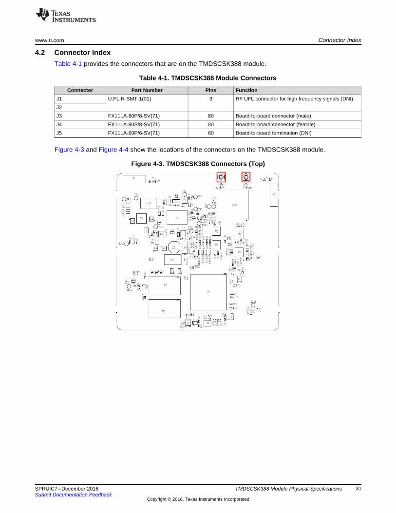
4.2 Connector IndexTable 4-1 provides the connectors that are on the TMDSCSK388 module.
Table 4-1. TMDSCSK388 Module Connectors
Connector Part Number Pins FunctionJ1 U.FL-R-SMT-1(01) 3 RF UFL connector for high frequency signals (DNI)J2J3 FX11LA-80P/8-SV(71) 80 Board-to-board connector (male)J4 FX11LA-80S/8-SV(71) 80 Board-to-board connector (female)J5 FX11LA-60P/6-SV(71) 60 Board-to-board termination (DNI)
Figure 4-3 and Figure 4-4 show the locations of the connectors on the TMDSCSK388 module.
Figure 4-3. TMDSCSK388 Connectors (Top)
Connector Index www.ti.com
32 SPRUIC7–December 2016Submit Documentation Feedback
Copyright © 2016, Texas Instruments Incorporated
TMDSCSK388 Module Physical Specifications
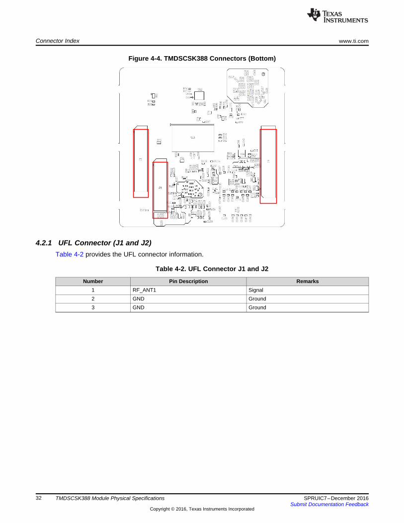
Figure 4-4. TMDSCSK388 Connectors (Bottom)
4.2.1 UFL Connector (J1 and J2)Table 4-2 provides the UFL connector information.
Table 4-2. UFL Connector J1 and J2
Number Pin Description Remarks1 RF_ANT1 Signal2 GND Ground3 GND Ground
www.ti.com Connector Index
33SPRUIC7–December 2016Submit Documentation Feedback
Copyright © 2016, Texas Instruments Incorporated
TMDSCSK388 Module Physical Specifications
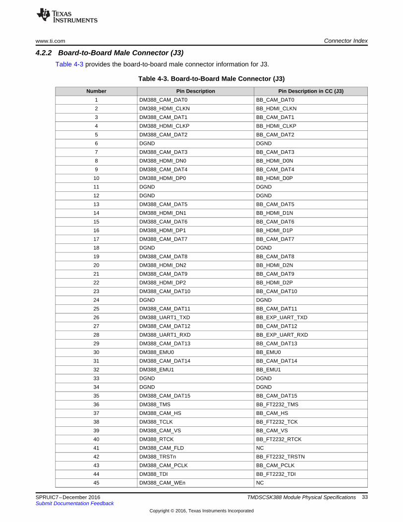
4.2.2 Board-to-Board Male Connector (J3)Table 4-3 provides the board-to-board male connector information for J3.
Table 4-3. Board-to-Board Male Connector (J3)
Number Pin Description Pin Description in CC (J3)1 DM388_CAM_DAT0 BB_CAM_DAT02 DM388_HDMI_CLKN BB_HDMI_CLKN3 DM388_CAM_DAT1 BB_CAM_DAT14 DM388_HDMI_CLKP BB_HDMI_CLKP5 DM388_CAM_DAT2 BB_CAM_DAT26 DGND DGND7 DM388_CAM_DAT3 BB_CAM_DAT38 DM388_HDMI_DN0 BB_HDMI_D0N9 DM388_CAM_DAT4 BB_CAM_DAT4
10 DM388_HDMI_DP0 BB_HDMI_D0P11 DGND DGND12 DGND DGND13 DM388_CAM_DAT5 BB_CAM_DAT514 DM388_HDMI_DN1 BB_HDMI_D1N15 DM388_CAM_DAT6 BB_CAM_DAT616 DM388_HDMI_DP1 BB_HDMI_D1P17 DM388_CAM_DAT7 BB_CAM_DAT718 DGND DGND19 DM388_CAM_DAT8 BB_CAM_DAT820 DM388_HDMI_DN2 BB_HDMI_D2N21 DM388_CAM_DAT9 BB_CAM_DAT922 DM388_HDMI_DP2 BB_HDMI_D2P23 DM388_CAM_DAT10 BB_CAM_DAT1024 DGND DGND25 DM388_CAM_DAT11 BB_CAM_DAT1126 DM388_UART1_TXD BB_EXP_UART_TXD27 DM388_CAM_DAT12 BB_CAM_DAT1228 DM388_UART1_RXD BB_EXP_UART_RXD29 DM388_CAM_DAT13 BB_CAM_DAT1330 DM388_EMU0 BB_EMU031 DM388_CAM_DAT14 BB_CAM_DAT1432 DM388_EMU1 BB_EMU133 DGND DGND34 DGND DGND35 DM388_CAM_DAT15 BB_CAM_DAT1536 DM388_TMS BB_FT2232_TMS37 DM388_CAM_HS BB_CAM_HS38 DM388_TCLK BB_FT2232_TCK39 DM388_CAM_VS BB_CAM_VS40 DM388_RTCK BB_FT2232_RTCK41 DM388_CAM_FLD NC42 DM388_TRSTn BB_FT2232_TRSTN43 DM388_CAM_PCLK BB_CAM_PCLK44 DM388_TDI BB_FT2232_TDI45 DM388_CAM_WEn NC
Connector Index www.ti.com
34 SPRUIC7–December 2016Submit Documentation Feedback
Copyright © 2016, Texas Instruments Incorporated
TMDSCSK388 Module Physical Specifications
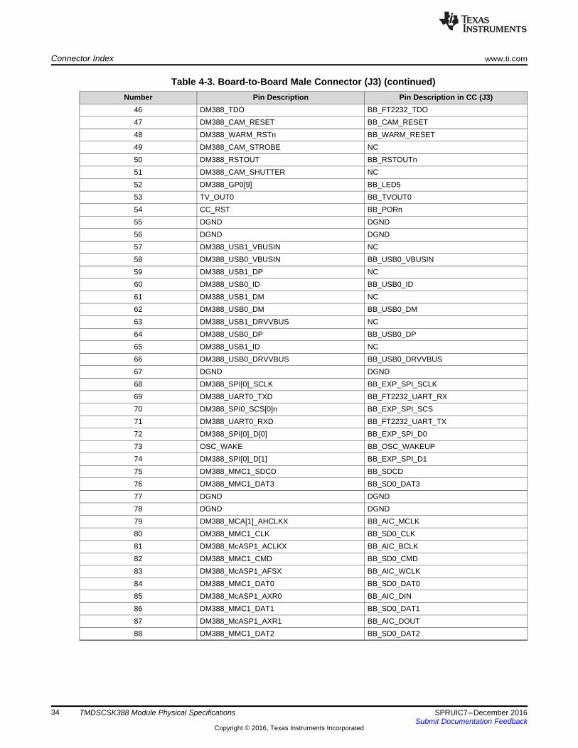
Table 4-3. Board-to-Board Male Connector (J3) (continued)Number Pin Description Pin Description in CC (J3)
46 DM388_TDO BB_FT2232_TDO47 DM388_CAM_RESET BB_CAM_RESET48 DM388_WARM_RSTn BB_WARM_RESET49 DM388_CAM_STROBE NC50 DM388_RSTOUT BB_RSTOUTn51 DM388_CAM_SHUTTER NC52 DM388_GP0[9] BB_LED553 TV_OUT0 BB_TVOUT054 CC_RST BB_PORn55 DGND DGND56 DGND DGND57 DM388_USB1_VBUSIN NC58 DM388_USB0_VBUSIN BB_USB0_VBUSIN59 DM388_USB1_DP NC60 DM388_USB0_ID BB_USB0_ID61 DM388_USB1_DM NC62 DM388_USB0_DM BB_USB0_DM63 DM388_USB1_DRVVBUS NC64 DM388_USB0_DP BB_USB0_DP65 DM388_USB1_ID NC66 DM388_USB0_DRVVBUS BB_USB0_DRVVBUS67 DGND DGND68 DM388_SPI[0]_SCLK BB_EXP_SPI_SCLK69 DM388_UART0_TXD BB_FT2232_UART_RX70 DM388_SPI0_SCS[0]n BB_EXP_SPI_SCS71 DM388_UART0_RXD BB_FT2232_UART_TX72 DM388_SPI[0]_D[0] BB_EXP_SPI_D073 OSC_WAKE BB_OSC_WAKEUP74 DM388_SPI[0]_D[1] BB_EXP_SPI_D175 DM388_MMC1_SDCD BB_SDCD76 DM388_MMC1_DAT3 BB_SD0_DAT377 DGND DGND78 DGND DGND79 DM388_MCA[1]_AHCLKX BB_AIC_MCLK80 DM388_MMC1_CLK BB_SD0_CLK81 DM388_McASP1_ACLKX BB_AIC_BCLK82 DM388_MMC1_CMD BB_SD0_CMD83 DM388_McASP1_AFSX BB_AIC_WCLK84 DM388_MMC1_DAT0 BB_SD0_DAT085 DM388_McASP1_AXR0 BB_AIC_DIN86 DM388_MMC1_DAT1 BB_SD0_DAT187 DM388_McASP1_AXR1 BB_AIC_DOUT88 DM388_MMC1_DAT2 BB_SD0_DAT2
www.ti.com Connector Index
35SPRUIC7–December 2016Submit Documentation Feedback
Copyright © 2016, Texas Instruments Incorporated
TMDSCSK388 Module Physical Specifications
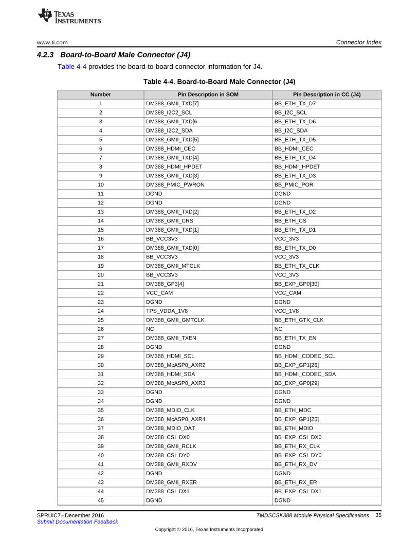
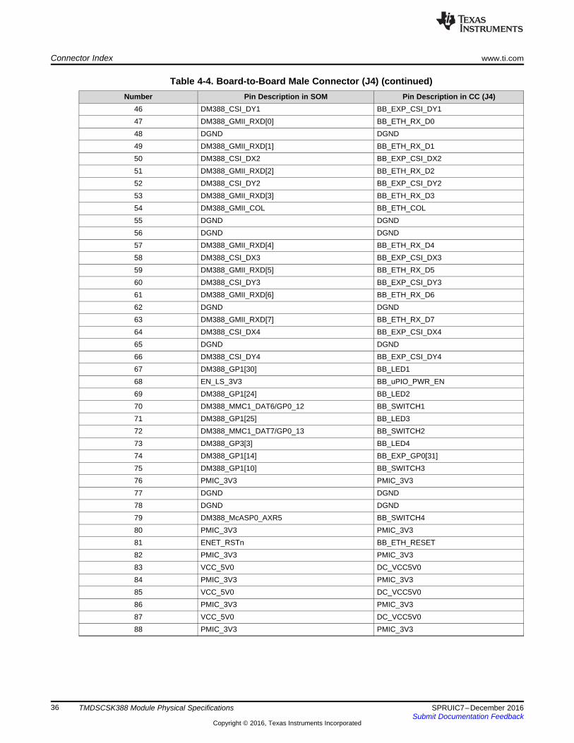
4.2.3 Board-to-Board Male Connector (J4)Table 4-4 provides the board-to-board connector information for J4.
Table 4-4. Board-to-Board Male Connector (J4)
Number Pin Description in SOM Pin Description in CC (J4)1 DM388_GMII_TXD[7] BB_ETH_TX_D72 DM388_I2C2_SCL BB_I2C_SCL3 DM388_GMII_TXD[6 BB_ETH_TX_D64 DM388_I2C2_SDA BB_I2C_SDA5 DM388_GMII_TXD[5] BB_ETH_TX_D56 DM388_HDMI_CEC BB_HDMI_CEC7 DM388_GMII_TXD[4] BB_ETH_TX_D48 DM388_HDMI_HPDET BB_HDMI_HPDET9 DM388_GMII_TXD[3] BB_ETH_TX_D310 DM388_PMIC_PWRON BB_PMIC_POR11 DGND DGND12 DGND DGND13 DM388_GMII_TXD[2] BB_ETH_TX_D214 DM388_GMII_CRS BB_ETH_CS15 DM388_GMII_TXD[1] BB_ETH_TX_D116 BB_VCC3V3 VCC_3V317 DM388_GMII_TXD[0] BB_ETH_TX_D018 BB_VCC3V3 VCC_3V319 DM388_GMII_MTCLK BB_ETH_TX_CLK20 BB_VCC3V3 VCC_3V321 DM388_GP3[4] BB_EXP_GP0[30]22 VCC_CAM VCC_CAM23 DGND DGND24 TPS_VDDA_1V8 VCC_1V825 DM388_GMII_GMTCLK BB_ETH_GTX_CLK26 NC NC27 DM388_GMII_TXEN BB_ETH_TX_EN28 DGND DGND29 DM388_HDMI_SCL BB_HDMI_CODEC_SCL30 DM388_McASP0_AXR2 BB_EXP_GP1[26]31 DM388_HDMI_SDA BB_HDMI_CODEC_SDA32 DM388_McASP0_AXR3 BB_EXP_GP0[29]33 DGND DGND34 DGND DGND35 DM388_MDIO_CLK BB_ETH_MDC36 DM388_McASP0_AXR4 BB_EXP_GP1[25]37 DM388_MDIO_DAT BB_ETH_MDIO38 DM388_CSI_DX0 BB_EXP_CSI_DX039 DM388_GMII_RCLK BB_ETH_RX_CLK40 DM388_CSI_DY0 BB_EXP_CSI_DY041 DM388_GMII_RXDV BB_ETH_RX_DV42 DGND DGND43 DM388_GMII_RXER BB_ETH_RX_ER44 DM388_CSI_DX1 BB_EXP_CSI_DX145 DGND DGND
Connector Index www.ti.com
36 SPRUIC7–December 2016Submit Documentation Feedback
Copyright © 2016, Texas Instruments Incorporated
TMDSCSK388 Module Physical Specifications
Table 4-4. Board-to-Board Male Connector (J4) (continued)Number Pin Description in SOM Pin Description in CC (J4)
46 DM388_CSI_DY1 BB_EXP_CSI_DY147 DM388_GMII_RXD[0] BB_ETH_RX_D048 DGND DGND49 DM388_GMII_RXD[1] BB_ETH_RX_D150 DM388_CSI_DX2 BB_EXP_CSI_DX251 DM388_GMII_RXD[2] BB_ETH_RX_D252 DM388_CSI_DY2 BB_EXP_CSI_DY253 DM388_GMII_RXD[3] BB_ETH_RX_D354 DM388_GMII_COL BB_ETH_COL55 DGND DGND56 DGND DGND57 DM388_GMII_RXD[4] BB_ETH_RX_D458 DM388_CSI_DX3 BB_EXP_CSI_DX359 DM388_GMII_RXD[5] BB_ETH_RX_D560 DM388_CSI_DY3 BB_EXP_CSI_DY361 DM388_GMII_RXD[6] BB_ETH_RX_D662 DGND DGND63 DM388_GMII_RXD[7] BB_ETH_RX_D764 DM388_CSI_DX4 BB_EXP_CSI_DX465 DGND DGND66 DM388_CSI_DY4 BB_EXP_CSI_DY467 DM388_GP1[30] BB_LED168 EN_LS_3V3 BB_uPIO_PWR_EN69 DM388_GP1[24] BB_LED270 DM388_MMC1_DAT6/GP0_12 BB_SWITCH171 DM388_GP1[25] BB_LED372 DM388_MMC1_DAT7/GP0_13 BB_SWITCH273 DM388_GP3[3] BB_LED474 DM388_GP1[14] BB_EXP_GP0[31]75 DM388_GP1[10] BB_SWITCH376 PMIC_3V3 PMIC_3V377 DGND DGND78 DGND DGND79 DM388_McASP0_AXR5 BB_SWITCH480 PMIC_3V3 PMIC_3V381 ENET_RSTn BB_ETH_RESET82 PMIC_3V3 PMIC_3V383 VCC_5V0 DC_VCC5V084 PMIC_3V3 PMIC_3V385 VCC_5V0 DC_VCC5V086 PMIC_3V3 PMIC_3V387 VCC_5V0 DC_VCC5V088 PMIC_3V3 PMIC_3V3
www.ti.com Connector Index
37SPRUIC7–December 2016Submit Documentation Feedback
Copyright © 2016, Texas Instruments Incorporated
TMDSCSK388 Module Physical Specifications
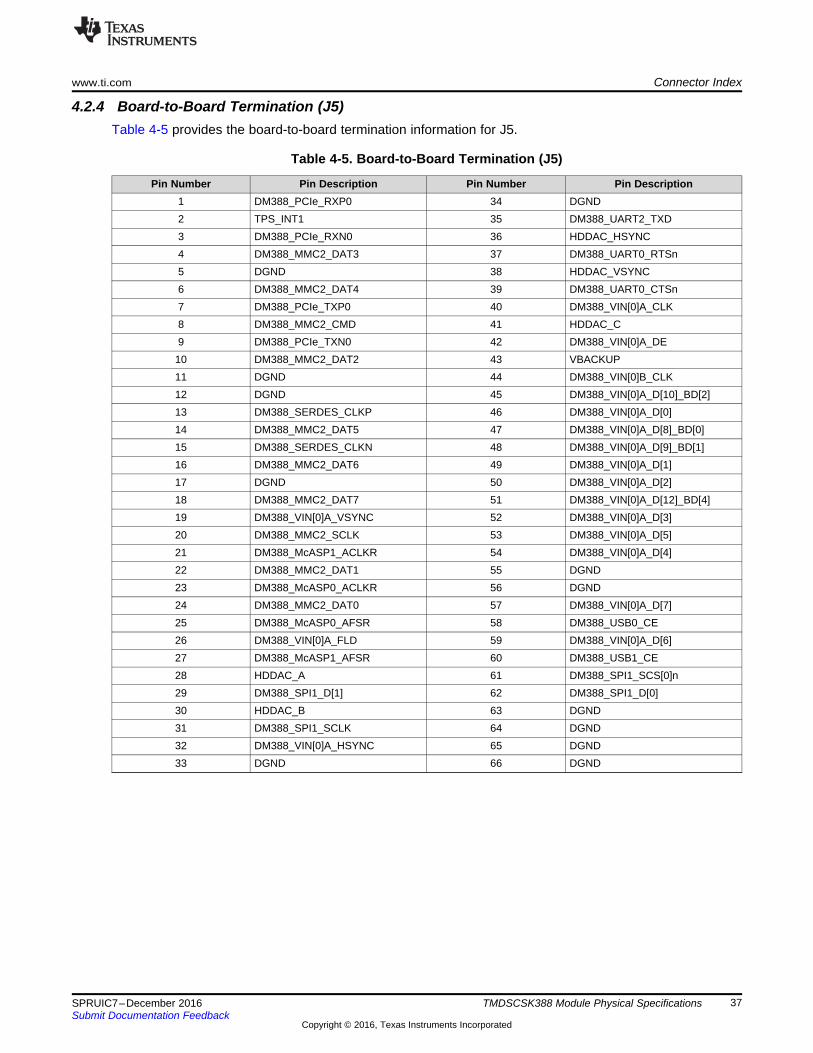
4.2.4 Board-to-Board Termination (J5)Table 4-5 provides the board-to-board termination information for J5.
Table 4-5. Board-to-Board Termination (J5)
Pin Number Pin Description Pin Number Pin Description1 DM388_PCIe_RXP0 34 DGND2 TPS_INT1 35 DM388_UART2_TXD3 DM388_PCIe_RXN0 36 HDDAC_HSYNC4 DM388_MMC2_DAT3 37 DM388_UART0_RTSn5 DGND 38 HDDAC_VSYNC6 DM388_MMC2_DAT4 39 DM388_UART0_CTSn7 DM388_PCIe_TXP0 40 DM388_VIN[0]A_CLK8 DM388_MMC2_CMD 41 HDDAC_C9 DM388_PCIe_TXN0 42 DM388_VIN[0]A_DE
10 DM388_MMC2_DAT2 43 VBACKUP11 DGND 44 DM388_VIN[0]B_CLK12 DGND 45 DM388_VIN[0]A_D[10]_BD[2]13 DM388_SERDES_CLKP 46 DM388_VIN[0]A_D[0]14 DM388_MMC2_DAT5 47 DM388_VIN[0]A_D[8]_BD[0]15 DM388_SERDES_CLKN 48 DM388_VIN[0]A_D[9]_BD[1]16 DM388_MMC2_DAT6 49 DM388_VIN[0]A_D[1]17 DGND 50 DM388_VIN[0]A_D[2]18 DM388_MMC2_DAT7 51 DM388_VIN[0]A_D[12]_BD[4]19 DM388_VIN[0]A_VSYNC 52 DM388_VIN[0]A_D[3]20 DM388_MMC2_SCLK 53 DM388_VIN[0]A_D[5]21 DM388_McASP1_ACLKR 54 DM388_VIN[0]A_D[4]22 DM388_MMC2_DAT1 55 DGND23 DM388_McASP0_ACLKR 56 DGND24 DM388_MMC2_DAT0 57 DM388_VIN[0]A_D[7]25 DM388_McASP0_AFSR 58 DM388_USB0_CE26 DM388_VIN[0]A_FLD 59 DM388_VIN[0]A_D[6]27 DM388_McASP1_AFSR 60 DM388_USB1_CE28 HDDAC_A 61 DM388_SPI1_SCS[0]n29 DM388_SPI1_D[1] 62 DM388_SPI1_D[0]30 HDDAC_B 63 DGND31 DM388_SPI1_SCLK 64 DGND32 DM388_VIN[0]A_HSYNC 65 DGND33 DGND 66 DGND
Switches, Test Points, and LEDs www.ti.com
38 SPRUIC7–December 2016Submit Documentation Feedback
Copyright © 2016, Texas Instruments Incorporated
TMDSCSK388 Module Physical Specifications
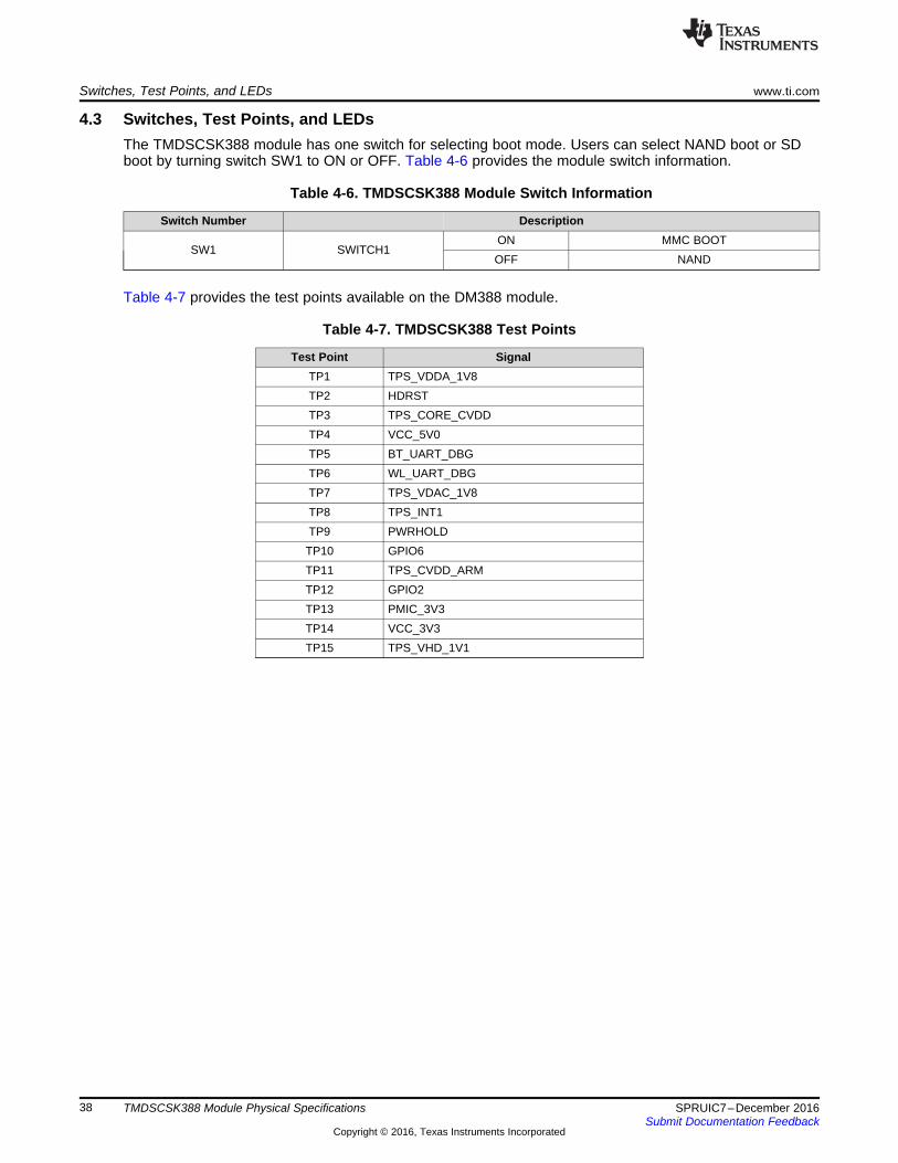
4.3 Switches, Test Points, and LEDsThe TMDSCSK388 module has one switch for selecting boot mode. Users can select NAND boot or SDboot by turning switch SW1 to ON or OFF. Table 4-6 provides the module switch information.
Table 4-6. TMDSCSK388 Module Switch Information
Switch Number Description
SW1 SWITCH1ON MMC BOOTOFF NAND
Table 4-7 provides the test points available on the DM388 module.
Table 4-7. TMDSCSK388 Test Points
Test Point SignalTP1 TPS_VDDA_1V8TP2 HDRSTTP3 TPS_CORE_CVDDTP4 VCC_5V0TP5 BT_UART_DBGTP6 WL_UART_DBGTP7 TPS_VDAC_1V8TP8 TPS_INT1TP9 PWRHOLDTP10 GPIO6TP11 TPS_CVDD_ARMTP12 GPIO2TP13 PMIC_3V3TP14 VCC_3V3TP15 TPS_VHD_1V1
TP14
SW1
TP13
TP11
TP4
TP3 TP8 TP1 TP2 TP5 TP6
TP7
LD1
TP9TP10
TP12
TP15
www.ti.com Switches, Test Points, and LEDs
39SPRUIC7–December 2016Submit Documentation Feedback
Copyright © 2016, Texas Instruments Incorporated
TMDSCSK388 Module Physical Specifications
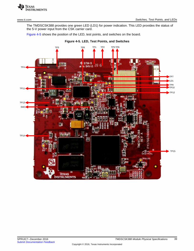
The TMDSCSK388 provides one green LED (LD1) for power indication. This LED provides the status ofthe 5-V power input from the CSK carrier card.
Figure 4-5 shows the position of the LED, test points, and switches on the board.
Figure 4-5. LED, Test Points, and Switches
40 SPRUIC7–December 2016Submit Documentation Feedback
Copyright © 2016, Texas Instruments Incorporated
TMDSCSK388 Power Requirements
Chapter 5SPRUIC7–December 2016
TMDSCSK388 Power Requirements
Topic ........................................................................................................................... Page
5.1 Power Distribution.............................................................................................. 415.2 Power Supply Calculation ................................................................................... 425.3 Power-up Sequence............................................................................................ 43
Board-to-Board Connectors (2)
PMICTPS6591133
DDR3 PowerTPS51216
LED
DDR3 (2)MT41K256M16TW107
VCC_5V0+5 V
VBACK UP
PMIC_3V3+3.3 V
VCC_3V3+3.3 V
EN_LS_3V3
LDOTPS71711DCKR
DM388 Processor
NAND FlashMT29F2G16ABAEAWP:E
MuxerSN74CBTLV3257RGYR
3 Input and GateSN74LVC1G11DCKR
Level TranslatorTXS0106ERGYR
Level Translator (3)SN74AVCT245RGYR
Wi-Fi and BT ModuleWL1837
Shunt RegulatorTLV431ACDBVR
VD
D_D
DR
, +1.5 V
VD
D_D
DR
_VR
EF
, +0.75 V
CV
DD
_AR
M, +
1.2 V
CV
DD
_HD
VIC
P, +
1.2 V
CO
RE
_CV
DD
, +1.2 V
TP
S_V
DD
A_1V
6, +1.6 V
VC
C_3V
3, +3.3 V
TP
S_V
HD
_1V1, +
1.1 V
HD
DA
C_V
RE
F, +
0.5 V
Copyright © 2016, Texas Instruments Incorporated
VDD_DDR+1.5 V
VDD_DDR_VREF+0.75 V
VDDR_VTT+0.75 V
EN_TPS51216
www.ti.com Power Distribution
41SPRUIC7–December 2016Submit Documentation Feedback
Copyright © 2016, Texas Instruments Incorporated
TMDSCSK388 Power Requirements
5.1 Power DistributionFigure 5-1 shows the power distribution diagram.
Figure 5-1. Power Distribution
Power Supply Calculation www.ti.com
42 SPRUIC7–December 2016Submit Documentation Feedback
Copyright © 2016, Texas Instruments Incorporated
TMDSCSK388 Power Requirements
5.2 Power Supply CalculationTable 5-1 provides the power supply calculations.
Table 5-1. Power Supply Calculations
PartNumber Quantity CVDD
CORE_CVDDCVDD_ARMPMIC VDD1
CVDD_HDVICP
PMIC VDD2VDD_1V8PMIC VIO
TPS51216VCC_1V5
TPS71711DCKR
TPS VHD1V1
VCC_3V3Carrier Card
DDR_VIT0.75 PMIC_3V3 VCC_5V0
TMS320DM388 1 1125 365 0 53 402 150 139 382.6968984DDR3MT41K256M16TW
4 520 272
MT29F4G16ABAEAWP 1 30
TXS0108EPWR 1 .036 .036 .108WL1837MOD 1 909.0909091SN74AVC4T245RGYR 3 300 300
SN74LVC1G11DCKR 1 100
SN74CBTLV3257RGYR 1 128
LED 1_Total (mA) 1125 365 0 353.036 922.036 1606.198909 272 382.6968984 320.6470588Input Voltage 5 3.3 3.3 3.3 5 3.3 5 1.5 5 5Efficiency 0.85 0.85 0.8 0.85 0.8 0.85 0.85 0.85 0.75Quiescent current(mA)Output voltage 1.2 1.2 1.2 1.8 1.5 1.1 3.3 0.75 3.3 3.3Current drawnfrom input 317.6470588 156.1497326 0 226.5471658 345.7635 150 1247.166212 160 297.1528858 504
Current drawnfrom VCC_5V0
2210.729656 mA
PORn
VDDA_1V8
VDD_DDR
VCC_3V3
TPS_CORE_CVDD
TPS_CVDD_ARM
TPS_CVDD_HDVICP
3.3 V
663.82 ms
10.64 ms
14.52 ms
16.88 ms
18.70 ms
20.72 ms
1.8 V
1.5 V
3.3 V
1.2 V
1.2 V
1.2 V
www.ti.com Power-up Sequence
43SPRUIC7–December 2016Submit Documentation Feedback
Copyright © 2016, Texas Instruments Incorporated
TMDSCSK388 Power Requirements
5.3 Power-up SequenceFigure 5-2 shows the power-up sequence required for the processor.
Figure 5-2. Power Sequencing
44 SPRUIC7–December 2016Submit Documentation Feedback
Copyright © 2016, Texas Instruments Incorporated
Overview of TMDSCSKCC
Chapter 6SPRUIC7–December 2016
Overview of TMDSCSKCC
Topic ........................................................................................................................... Page
6.1 Key Features ..................................................................................................... 456.2 Block Diagram ................................................................................................... 466.3 Power Supply .................................................................................................... 496.4 Overvoltage Protection Circuit............................................................................. 50
www.ti.com Key Features
45SPRUIC7–December 2016Submit Documentation Feedback
Copyright © 2016, Texas Instruments Incorporated
Overview of TMDSCSKCC
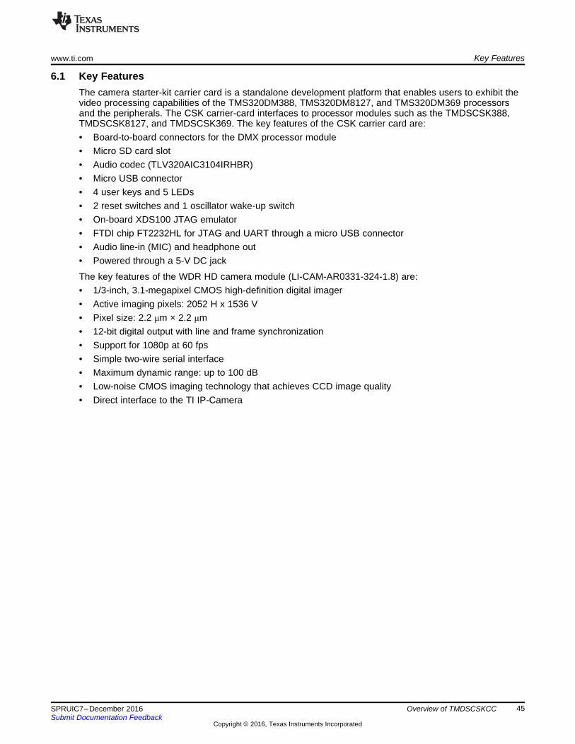
6.1 Key FeaturesThe camera starter-kit carrier card is a standalone development platform that enables users to exhibit thevideo processing capabilities of the TMS320DM388, TMS320DM8127, and TMS320DM369 processorsand the peripherals. The CSK carrier-card interfaces to processor modules such as the TMDSCSK388,TMDSCSK8127, and TMDSCSK369. The key features of the CSK carrier card are:• Board-to-board connectors for the DMX processor module• Micro SD card slot• Audio codec (TLV320AIC3104IRHBR)• Micro USB connector• 4 user keys and 5 LEDs• 2 reset switches and 1 oscillator wake-up switch• On-board XDS100 JTAG emulator• FTDI chip FT2232HL for JTAG and UART through a micro USB connector• Audio line-in (MIC) and headphone out• Powered through a 5-V DC jack
The key features of the WDR HD camera module (LI-CAM-AR0331-324-1.8) are:• 1/3-inch, 3.1-megapixel CMOS high-definition digital imager• Active imaging pixels: 2052 H x 1536 V• Pixel size: 2.2 μm × 2.2 μm• 12-bit digital output with line and frame synchronization• Support for 1080p at 60 fps• Simple two-wire serial interface• Maximum dynamic range: up to 100 dB• Low-noise CMOS imaging technology that achieves CCD image quality• Direct interface to the TI IP-Camera
Ethernet PHYDP83867IRPAP
24.576 MHz
Audio CodecTLV320AIC3106
MMC
USB0
McASP, I2C
LDOTLV1117-33
Level Translator
80-Pin Board-to-Board
Connector
Parallel Camera ConnectorFH12A-36S-0.55H(55)
80-Pin Board-to-Board
Connector
60-Pin Expansion Connector
SPI, UART4, and GPIO
CSI and I2C
UART,JTAG
3.5-mm jack
Headphone out and mic in
5-V input
FT2232HL
EEPROMAT93C46D
12 MHz
Micro SD
USB0
Video Filter
ESD and Level Translator
TPD12S016
CAM
VOUT COM
FPC Cable
HDMI
Debug USB
3.3-V PMIC and Peripherals5-V inputPower
input
Reset switches LEDs
Switches
Copyright © 2016, Texas Instruments Incorporated
Block Diagram www.ti.com
46 SPRUIC7–December 2016Submit Documentation Feedback
Copyright © 2016, Texas Instruments Incorporated
Overview of TMDSCSKCC
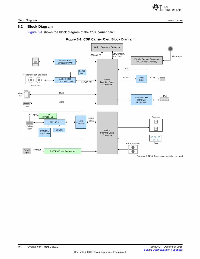
6.2 Block DiagramFigure 6-1 shows the block diagram of the CSK carrier card.
Figure 6-1. CSK Carrier Card Block Diagram
www.ti.com Block Diagram
47SPRUIC7–December 2016Submit Documentation Feedback
Copyright © 2016, Texas Instruments Incorporated
Overview of TMDSCSKCC
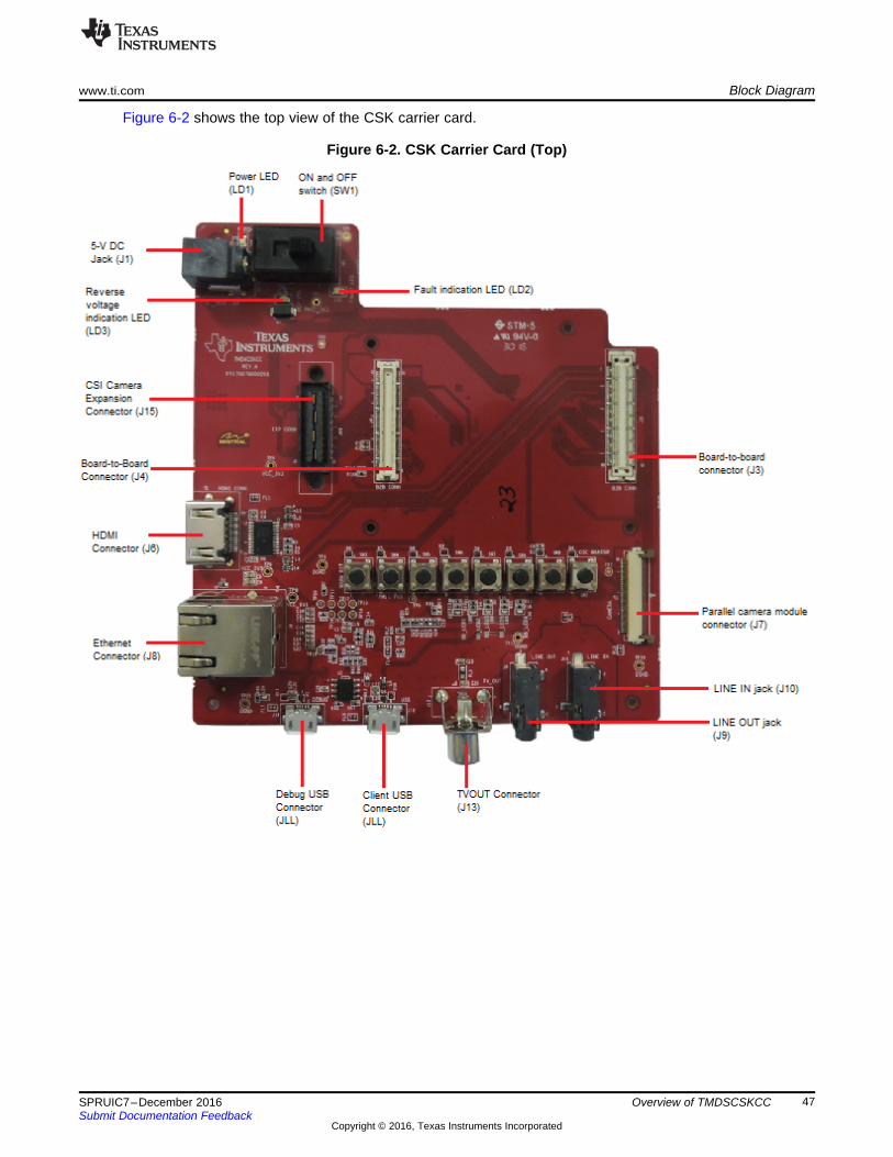
Figure 6-2 shows the top view of the CSK carrier card.
Figure 6-2. CSK Carrier Card (Top)
MICRO SD CARDCONN (J14)
Block Diagram www.ti.com
48 SPRUIC7–December 2016Submit Documentation Feedback
Copyright © 2016, Texas Instruments Incorporated
Overview of TMDSCSKCC
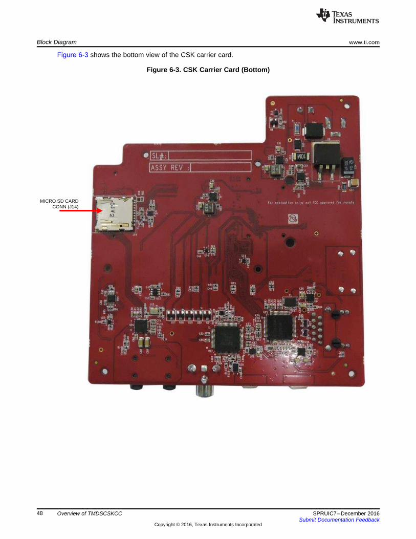
Figure 6-3 shows the bottom view of the CSK carrier card.
Figure 6-3. CSK Carrier Card (Bottom)
www.ti.com Power Supply
49SPRUIC7–December 2016Submit Documentation Feedback
Copyright © 2016, Texas Instruments Incorporated
Overview of TMDSCSKCC
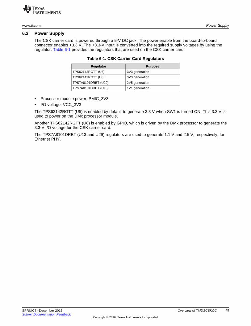
6.3 Power SupplyThe CSK carrier card is powered through a 5-V DC jack. The power enable from the board-to-boardconnector enables +3.3 V. The +3.3-V input is converted into the required supply voltages by using theregulator. Table 6-1 provides the regulators that are used on the CSK carrier card.
Table 6-1. CSK Carrier Card Regulators
Regulator PurposeTPS62142RGTT (U5) 3V3 generationTPS62142RGTT (U8) 3V3 generationTPS7A8101DRBT (U29) 2V5 generationTPS7A8101DRBT (U13) 1V1 generation
• Processor module power: PMIC_3V3• I/O voltage: VCC_3V3
The TPS62142RGTT (U5) is enabled by default to generate 3.3 V when SW1 is turned ON. This 3.3 V isused to power on the DMx processor module.
Another TPS62142RGTT (U8) is enabled by GPIO, which is driven by the DMx processor to generate the3.3-V I/O voltage for the CSK carrier card.
The TPS7A8101DRBT (U13 and U29) regulators are used to generate 1.1 V and 2.5 V, respectively, forEthernet PHY.
Overvoltage Protection Circuit www.ti.com
50 SPRUIC7–December 2016Submit Documentation Feedback
Copyright © 2016, Texas Instruments Incorporated
Overview of TMDSCSKCC
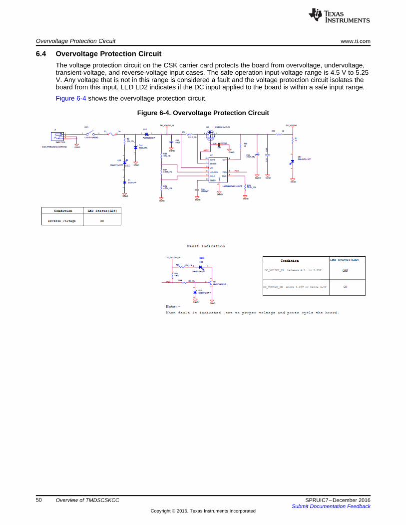
6.4 Overvoltage Protection CircuitThe voltage protection circuit on the CSK carrier card protects the board from overvoltage, undervoltage,transient-voltage, and reverse-voltage input cases. The safe operation input-voltage range is 4.5 V to 5.25V. Any voltage that is not in this range is considered a fault and the voltage protection circuit isolates theboard from this input. LED LD2 indicates if the DC input applied to the board is within a safe input range.
Figure 6-4 shows the overvoltage protection circuit.
Figure 6-4. Overvoltage Protection Circuit
51SPRUIC7–December 2016Submit Documentation Feedback
Copyright © 2016, Texas Instruments Incorporated
CSK Carrier Card Interface
Chapter 7SPRUIC7–December 2016
CSK Carrier Card Interface
Topic ........................................................................................................................... Page
7.1 XDS100 On-Board Emulator Interface ................................................................... 527.2 Clock Distribution .............................................................................................. 537.3 Reset Circuit and Distribution.............................................................................. 547.4 Camera Interface ................................................................................................ 557.5 Ethernet Interface............................................................................................... 567.6 HDMI and TVOUT Interfaces ................................................................................ 577.7 LED and Switch Interface .................................................................................... 577.8 Micro SD Card Interface ...................................................................................... 587.9 Audio Codec Interface ........................................................................................ 587.10 USB Interface..................................................................................................... 597.11 UART Interface................................................................................................... 597.12 I2C Interface ....................................................................................................... 607.13 Connection Between Expansion Connector and CSK Carrier Card........................... 60
Micro USB Connector
(J11)Client
5 V
LDOTLV1117-33CDCY
V3_3FTDI
FT2232HL
VPHY VPLL VREGIN VCCIO
V3_3FTDI
ESDDiodes
DMDP
AT93C46D
EECS
EESK
EEDATA
2.2 K
10 K
V3_3FTDI
V3_3FTDI
12 MHz
Level Translator
TCK
RTCK
TDO
TMS
TRST
UART_TX
UART_RX
EMU0:1
TDI
TCK
TDO
TMS
TRST
UART_TX
UART_RX
EMU0:1
TDI
Board-to-Board Connector
EMU0 EMU1
V3_3FTDI 3.3 V
4.7 K
4.7 K
3.3 V
CS
SK
DIN
DOUTORG
Copyright © 2016, Texas Instruments Incorporated
XDS100 On-Board Emulator Interface www.ti.com
52 SPRUIC7–December 2016Submit Documentation Feedback
Copyright © 2016, Texas Instruments Incorporated
CSK Carrier Card Interface
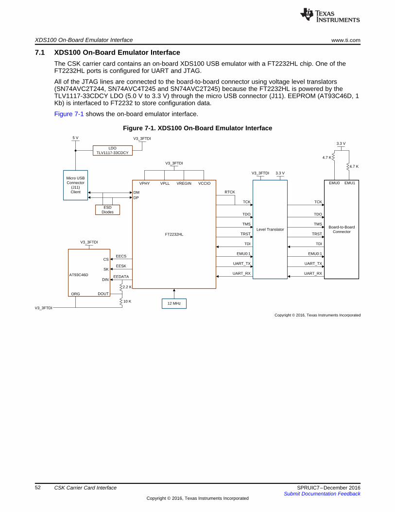
7.1 XDS100 On-Board Emulator InterfaceThe CSK carrier card contains an on-board XDS100 USB emulator with a FT2232HL chip. One of theFT2232HL ports is configured for UART and JTAG.
All of the JTAG lines are connected to the board-to-board connector using voltage level translators(SN74AVC2T244, SN74AVC4T245 and SN74AVC2T245) because the FT2232HL is powered by theTLV1117-33CDCY LDO (5.0 V to 3.3 V) through the micro USB connector (J11). EEPROM (AT93C46D, 1Kb) is interfaced to FT2232 to store configuration data.
Figure 7-1 shows the on-board emulator interface.
Figure 7-1. XDS100 On-Board Emulator Interface
Boa
rd-t
o-B
oard
Con
nect
or
DNI Audio CodecAIC3104
24.576-MHz OscillatorASE-24.576MHZ-LC-T
3.3 V
24.576 MHz
DP83867IRPAPT
25 MHz
FT2232HL
12-MHz OscillatorASDMB-12.00MHZ-LC-T
3.3 V
24.576 MHz
XI XO
Copyright © 2016, Texas Instruments Incorporated
www.ti.com Clock Distribution
53SPRUIC7–December 2016Submit Documentation Feedback
Copyright © 2016, Texas Instruments Incorporated
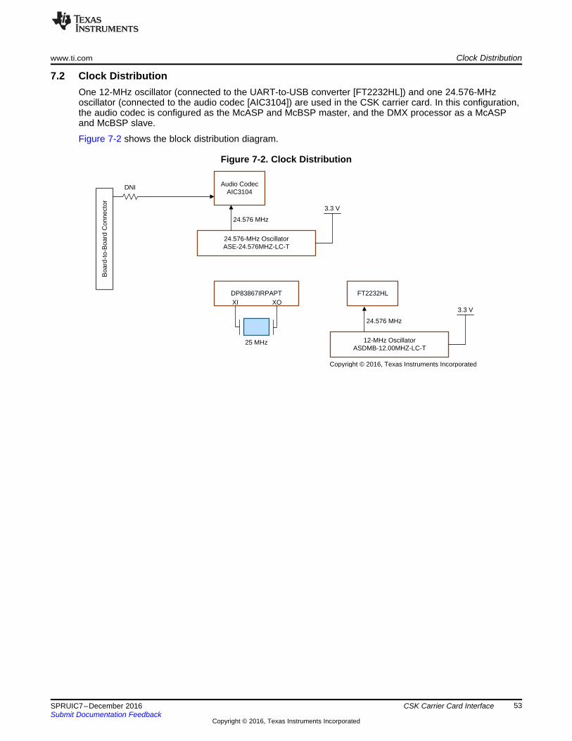
CSK Carrier Card Interface
7.2 Clock DistributionOne 12-MHz oscillator (connected to the UART-to-USB converter [FT2232HL]) and one 24.576-MHzoscillator (connected to the audio codec [AIC3104]) are used in the CSK carrier card. In this configuration,the audio codec is configured as the McASP and McBSP master, and the DMX processor as a McASPand McBSP slave.
Figure 7-2 shows the block distribution diagram.
Figure 7-2. Clock Distribution
Boa
rd-t
o-B
oard
Con
nect
or
RESET Supervisor
AN
D
AN
DA
ND
FT2232HL
Camera Connector
SW9
SW3
5 V
Ethernet PHY
Audio Codec
FT2232HL
BB_PORn
WARM_RESET
BB_CAM_RESET
BB_RSTOUTn
BB_ETH_RESET
CAM_RESET
ETH_RESET
Copyright © 2016, Texas Instruments Incorporated
Reset Circuit and Distribution www.ti.com
54 SPRUIC7–December 2016Submit Documentation Feedback
Copyright © 2016, Texas Instruments Incorporated
CSK Carrier Card Interface
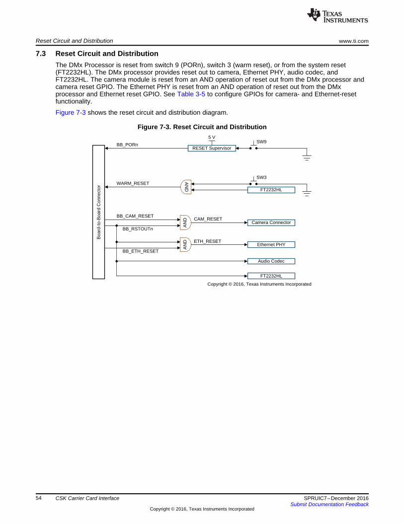
7.3 Reset Circuit and DistributionThe DMx Processor is reset from switch 9 (PORn), switch 3 (warm reset), or from the system reset(FT2232HL). The DMx processor provides reset out to camera, Ethernet PHY, audio codec, andFT2232HL. The camera module is reset from an AND operation of reset out from the DMx processor andcamera reset GPIO. The Ethernet PHY is reset from an AND operation of reset out from the DMxprocessor and Ethernet reset GPIO. See Table 3-5 to configure GPIOs for camera- and Ethernet-resetfunctionality.
Figure 7-3 shows the reset circuit and distribution diagram.
Figure 7-3. Reset Circuit and Distribution
Board-to-Board Connector
Camera Connector
Voltage Level Translator
AND
CAM_DAT0:15CAM_DAT0:15
CAM_VS
CAM_HS
CAM_PCLK
CAM_RESET
CAM_I2C_SCL
CAM_I2C_SDABB_I2C_SDA
BB_I2C_SCL
CAM_RESETBB_CAM_RESET
BB_RSTOUTn
CAM_VS
CAM_HS
CAM_PCLK
3.3 V 5.0 V
Copyright © 2016, Texas Instruments Incorporated
www.ti.com Camera Interface
55SPRUIC7–December 2016Submit Documentation Feedback
Copyright © 2016, Texas Instruments Incorporated
CSK Carrier Card Interface
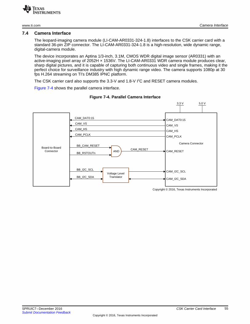
7.4 Camera InterfaceThe leopard-imaging camera module (LI-CAM-AR0331-324-1.8) interfaces to the CSK carrier card with astandard 36-pin ZIP connector. The LI-CAM-AR0331-324-1.8 is a high-resolution, wide dynamic range,digital-camera module.
The device incorporates an Aptina 1/3-inch, 3.1M, CMOS WDR digital image sensor (AR0331) with anactive-imaging pixel array of 2052H × 1536V. The LI-CAM-AR0331 WDR camera module produces clear,sharp digital pictures, and it is capable of capturing both continuous video and single frames, making it theperfect choice for surveillance industry with high dynamic range video. The camera supports 1080p at 30fps H.264 streaming on TI's DM385 IPNC platform.
The CSK carrier card also supports the 3.3-V and 1.8-V I2C and RESET camera modules.
Figure 7-4 shows the parallel camera interface.
Figure 7-4. Parallel Camera Interface
Boa
rd-t
o-B
oard
Con
nect
or
DP83867IRPAPT
ETH_RESET
BB_ETH_MDIO
BB_ETH_MDC
BB_ETH_RX_ER
BB_ETH_RX_CLK
BB_ETH_RX_DV
BB_ETH_GTX_CLK
BB_ETH_TX_CLK
BB_ETH_TX_EN
BB_ETH_RX_D0:7
BB_ETH_TX_D0:7
2.5 V 1.1 V 3.3 V
25 MHz
Eth
erne
t C
onne
ctor
ETHER_D0:3P/N
XI XO
Copyright © 2016, Texas Instruments Incorporated
Ethernet Interface www.ti.com
56 SPRUIC7–December 2016Submit Documentation Feedback
Copyright © 2016, Texas Instruments Incorporated
CSK Carrier Card Interface
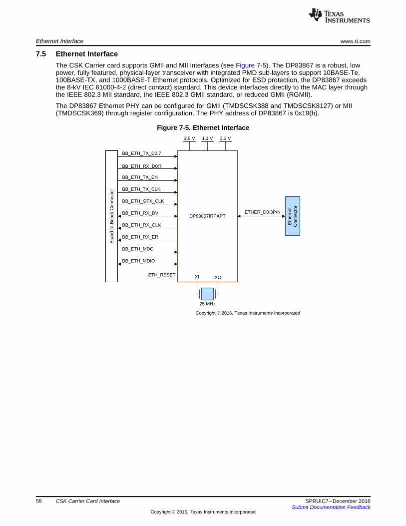
7.5 Ethernet InterfaceThe CSK Carrier card supports GMII and MII interfaces (see Figure 7-5). The DP83867 is a robust, lowpower, fully featured, physical-layer transceiver with integrated PMD sub-layers to support 10BASE-Te,100BASE-TX, and 1000BASE-T Ethernet protocols. Optimized for ESD protection, the DP83867 exceedsthe 8-kV IEC 61000-4-2 (direct contact) standard. This device interfaces directly to the MAC layer throughthe IEEE 802.3 MII standard, the IEEE 802.3 GMII standard, or reduced GMII (RGMII).
The DP83867 Ethernet PHY can be configured for GMII (TMDSCSK388 and TMDSCSK8127) or MII(TMDSCSK369) through register configuration. The PHY address of DP83867 is 0x19(h).
Figure 7-5. Ethernet Interface
SW8
SW7
SW6
SW5
Boa
rd-t
o-B
oard
Con
nect
or
3.3 V
LD7
LD8
LD4
LD6
LD5
Board-to-Board Connector
RCA Jack Connector
Common-mode Choke90E
ESD ProtectionTPD12S016PWR
HDMI Connector
BB_HDMI_DP[0:2]
BB_HDMI_DN[0:2] HDMI_DN[0:2]
HDMI_DP[0:2]
Copyright © 2016, Texas Instruments Incorporated
www.ti.com HDMI and TVOUT Interfaces
57SPRUIC7–December 2016Submit Documentation Feedback
Copyright © 2016, Texas Instruments Incorporated
CSK Carrier Card Interface
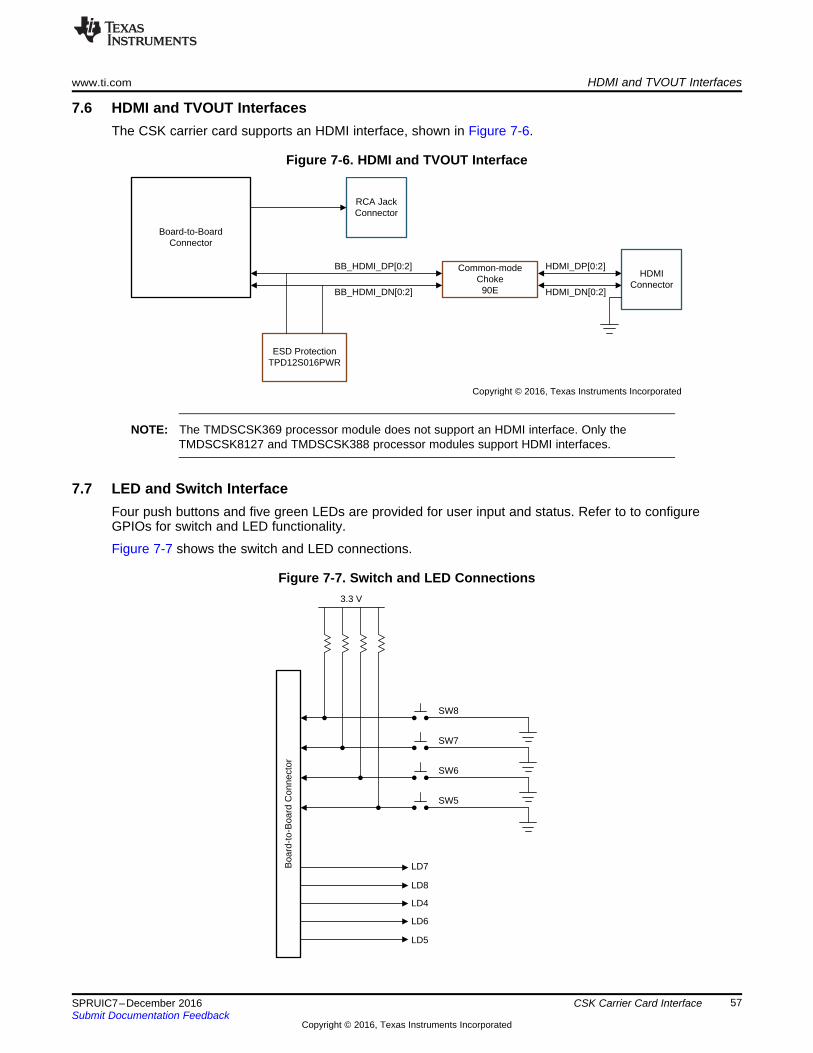
7.6 HDMI and TVOUT InterfacesThe CSK carrier card supports an HDMI interface, shown in Figure 7-6.
Figure 7-6. HDMI and TVOUT Interface
NOTE: The TMDSCSK369 processor module does not support an HDMI interface. Only theTMDSCSK8127 and TMDSCSK388 processor modules support HDMI interfaces.
7.7 LED and Switch InterfaceFour push buttons and five green LEDs are provided for user input and status. Refer to to configureGPIOs for switch and LED functionality.
Figure 7-7 shows the switch and LED connections.
Figure 7-7. Switch and LED Connections
Board-to-Board Connector
Audio Codec(AIC3104)
BB_AIC_DIN
BB_AIC_DOUT
BB_AIC_MCLK
BB_AIC_BCLK
BB_AIC_WCLK
BB_I2C_SDA
BB_I2C_SCL
HP ROUT
HP LOUT
MIC IN
24.576 MHz
1.8 V 3.3 V
Copyright © 2016, Texas Instruments Incorporated
Boa
rd-t
o-B
oard
Con
nect
or
Micro SDCard Connect
CLK
CMD
D[0-4]
Card Detect
BB_SD_CLK
BB_SD_CMD
BB_SD_D(0-4)
BB_SDCD
3.3 V
Micro SD Card Interface www.ti.com
58 SPRUIC7–December 2016Submit Documentation Feedback
Copyright © 2016, Texas Instruments Incorporated
CSK Carrier Card Interface
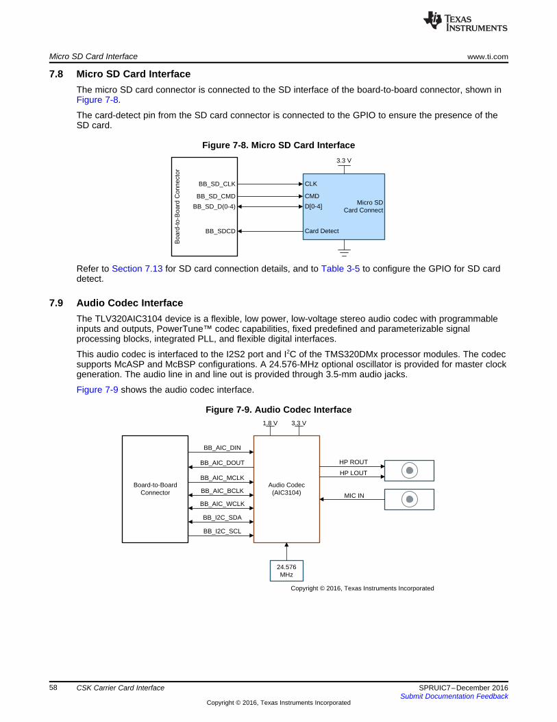
7.8 Micro SD Card InterfaceThe micro SD card connector is connected to the SD interface of the board-to-board connector, shown inFigure 7-8.
The card-detect pin from the SD card connector is connected to the GPIO to ensure the presence of theSD card.
Figure 7-8. Micro SD Card Interface
Refer to Section 7.13 for SD card connection details, and to Table 3-5 to configure the GPIO for SD carddetect.
7.9 Audio Codec InterfaceThe TLV320AIC3104 device is a flexible, low power, low-voltage stereo audio codec with programmableinputs and outputs, PowerTune™ codec capabilities, fixed predefined and parameterizable signalprocessing blocks, integrated PLL, and flexible digital interfaces.
This audio codec is interfaced to the I2S2 port and I2C of the TMS320DMx processor modules. The codecsupports McASP and McBSP configurations. A 24.576-MHz optional oscillator is provided for master clockgeneration. The audio line in and line out is provided through 3.5-mm audio jacks.
Figure 7-9 shows the audio codec interface.
Figure 7-9. Audio Codec Interface
Boa
rd-t
o-B
oard
Con
nect
or
FT2232HL
BB_FT2232_UART_TX
BB_FT2232_UART_RX
ESD ProtectionTPD12S016PWR
FT2232_USB_DM
FT2232_USB_DP
Micro USB Connector
Copyright © 2016, Texas Instruments Incorporated
Boa
rd-t
o-B
oard
Con
nect
or
Common Mode Choke90E
ESD DiodesTPD2EUSB30
Micro USB Connector
Power Distribution Switch
TPS2051B
DMDP
DMDP
ID
USB0_DRVVBUSUSB0_VBUS
DC_VCC5V0
Copyright © 2016, Texas Instruments Incorporated
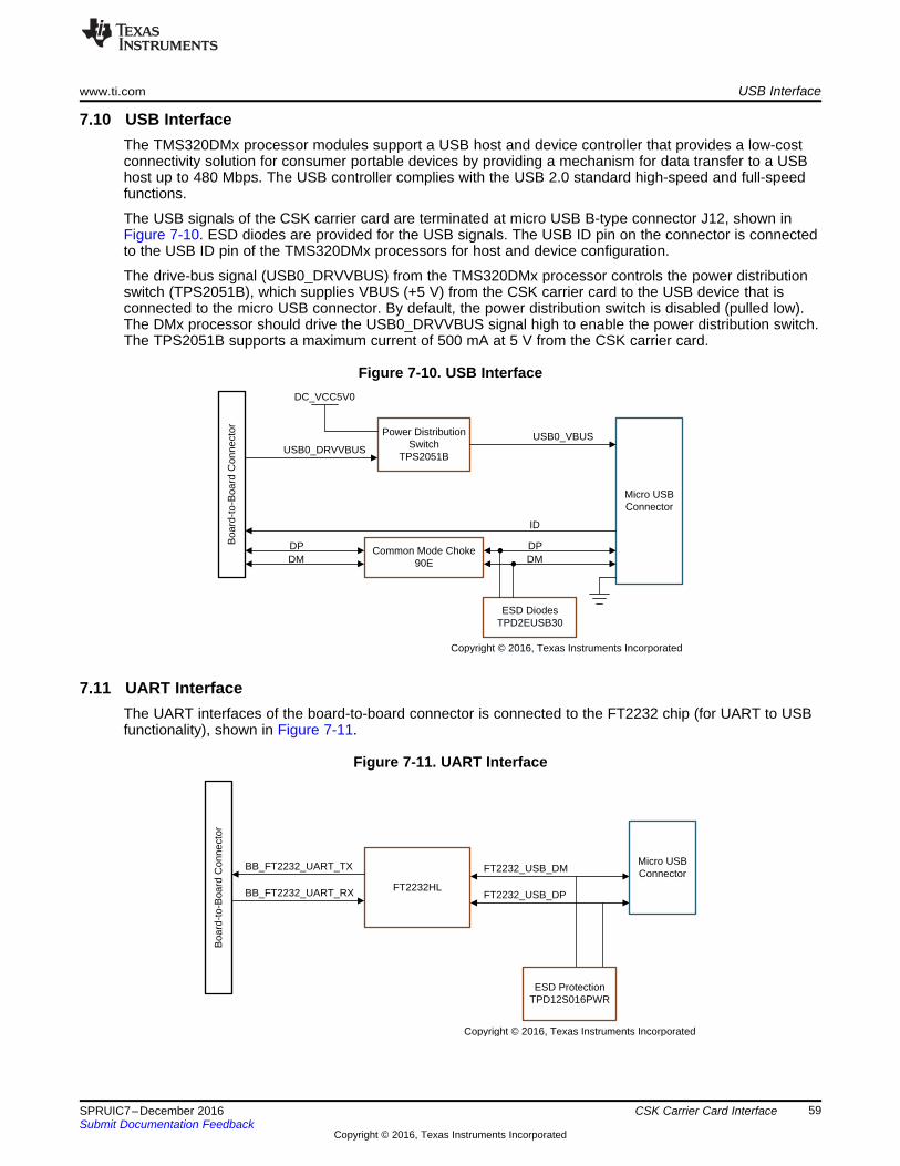
www.ti.com USB Interface
59SPRUIC7–December 2016Submit Documentation Feedback
Copyright © 2016, Texas Instruments Incorporated
CSK Carrier Card Interface
7.10 USB InterfaceThe TMS320DMx processor modules support a USB host and device controller that provides a low-costconnectivity solution for consumer portable devices by providing a mechanism for data transfer to a USBhost up to 480 Mbps. The USB controller complies with the USB 2.0 standard high-speed and full-speedfunctions.
The USB signals of the CSK carrier card are terminated at micro USB B-type connector J12, shown inFigure 7-10. ESD diodes are provided for the USB signals. The USB ID pin on the connector is connectedto the USB ID pin of the TMS320DMx processors for host and device configuration.
The drive-bus signal (USB0_DRVVBUS) from the TMS320DMx processor controls the power distributionswitch (TPS2051B), which supplies VBUS (+5 V) from the CSK carrier card to the USB device that isconnected to the micro USB connector. By default, the power distribution switch is disabled (pulled low).The DMx processor should drive the USB0_DRVVBUS signal high to enable the power distribution switch.The TPS2051B supports a maximum current of 500 mA at 5 V from the CSK carrier card.
Figure 7-10. USB Interface
7.11 UART InterfaceThe UART interfaces of the board-to-board connector is connected to the FT2232 chip (for UART to USBfunctionality), shown in Figure 7-11.
Figure 7-11. UART Interface
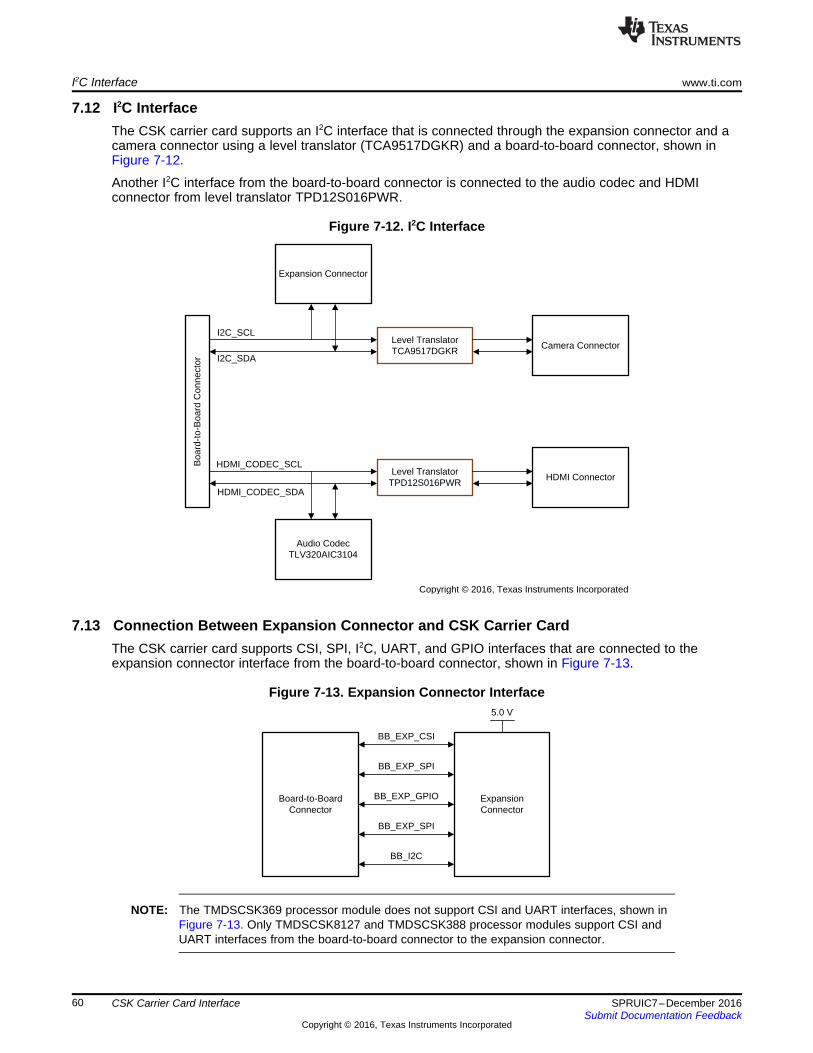
Board-to-Board Connector
Expansion Connector
BB_EXP_CSI
BB_EXP_SPI
BB_EXP_GPIO
BB_EXP_SPI
BB_I2C
5.0 V
Boa
rd-t
o-B
oard
Con
nect
or
Expansion Connector
Audio CodecTLV320AIC3104
I2C_SCL
I2C_SDA
HDMI_CODEC_SCL
HDMI_CODEC_SDA
Camera Connector
HDMI Connector
Level TranslatorTCA9517DGKR
Level TranslatorTPD12S016PWR
Copyright © 2016, Texas Instruments Incorporated
I2C Interface www.ti.com
60 SPRUIC7–December 2016Submit Documentation Feedback
Copyright © 2016, Texas Instruments Incorporated
CSK Carrier Card Interface
7.12 I2C InterfaceThe CSK carrier card supports an I2C interface that is connected through the expansion connector and acamera connector using a level translator (TCA9517DGKR) and a board-to-board connector, shown inFigure 7-12.
Another I2C interface from the board-to-board connector is connected to the audio codec and HDMIconnector from level translator TPD12S016PWR.
Figure 7-12. I2C Interface
7.13 Connection Between Expansion Connector and CSK Carrier CardThe CSK carrier card supports CSI, SPI, I2C, UART, and GPIO interfaces that are connected to theexpansion connector interface from the board-to-board connector, shown in Figure 7-13.
Figure 7-13. Expansion Connector Interface
NOTE: The TMDSCSK369 processor module does not support CSI and UART interfaces, shown inFigure 7-13. Only TMDSCSK8127 and TMDSCSK388 processor modules support CSI andUART interfaces from the board-to-board connector to the expansion connector.
61SPRUIC7–December 2016Submit Documentation Feedback
Copyright © 2016, Texas Instruments Incorporated
CSK Carrier Board Physical Specifications
Chapter 8SPRUIC7–December 2016
CSK Carrier Board Physical Specifications
Topic ........................................................................................................................... Page
8.1 Board Layout ..................................................................................................... 628.2 Connector Index................................................................................................. 64
8.2.1 DC Power Jack (J1) .................................................................................... 678.2.2 Board-to-Board Connector (J3) ....................................................................... 678.2.3 Board-to-Board Connector (J4) ....................................................................... 698.2.4 Expansion Connector (J15) ........................................................................... 708.2.5 HDMI Out Type-A Connector (J6).................................................................... 718.2.6 Camera FPC Connector (J7) ......................................................................... 718.2.7 RJ45 Connector (J8) ................................................................................... 728.2.8 Stereo-Audio Jack (J9 and J10) ...................................................................... 728.2.9 Micro USB Connector (J11 and J12) ................................................................ 738.2.10 Composite Video OUT RCA Connector (J13) ..................................................... 738.2.11 Micro SD Card Connector (J14) ..................................................................... 73
8.3 Push Buttons..................................................................................................... 748.4 Test Points ........................................................................................................ 748.5 System LEDs ..................................................................................................... 75
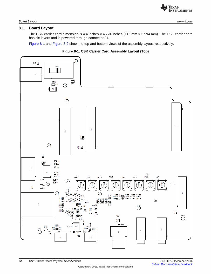
Board Layout www.ti.com
62 SPRUIC7–December 2016Submit Documentation Feedback
Copyright © 2016, Texas Instruments Incorporated
CSK Carrier Board Physical Specifications
8.1 Board LayoutThe CSK carrier card dimension is 4.4 inches × 4.724 inches (116 mm × 37.94 mm). The CSK carrier cardhas six layers and is powered through connector J1.
Figure 8-1 and Figure 8-2 show the top and bottom views of the assembly layout, respectively.
Figure 8-1. CSK Carrier Card Assembly Layout (Top)
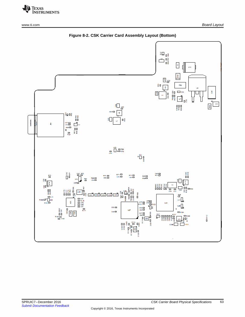
www.ti.com Board Layout
63SPRUIC7–December 2016Submit Documentation Feedback
Copyright © 2016, Texas Instruments Incorporated
CSK Carrier Board Physical Specifications
Figure 8-2. CSK Carrier Card Assembly Layout (Bottom)
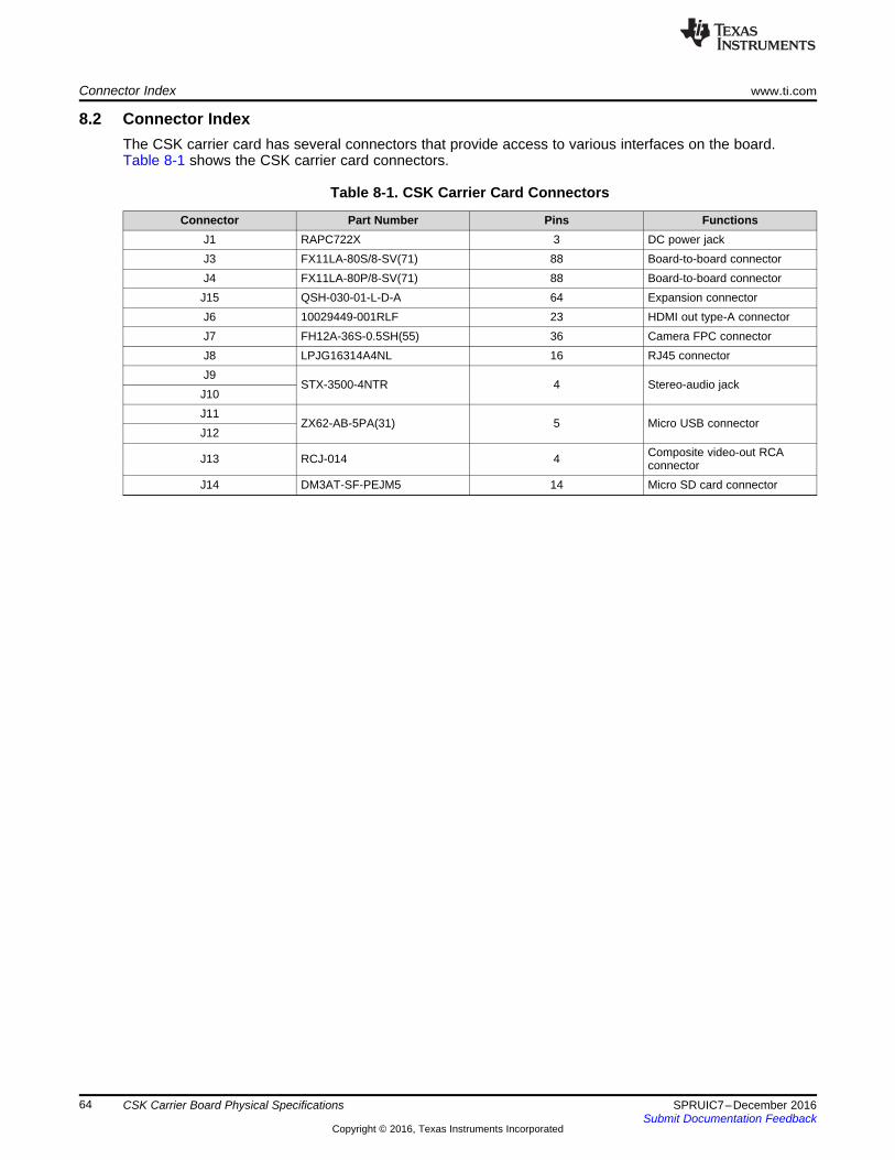
Connector Index www.ti.com
64 SPRUIC7–December 2016Submit Documentation Feedback
Copyright © 2016, Texas Instruments Incorporated
CSK Carrier Board Physical Specifications
8.2 Connector IndexThe CSK carrier card has several connectors that provide access to various interfaces on the board.Table 8-1 shows the CSK carrier card connectors.
Table 8-1. CSK Carrier Card Connectors
Connector Part Number Pins FunctionsJ1 RAPC722X 3 DC power jackJ3 FX11LA-80S/8-SV(71) 88 Board-to-board connectorJ4 FX11LA-80P/8-SV(71) 88 Board-to-board connectorJ15 QSH-030-01-L-D-A 64 Expansion connectorJ6 10029449-001RLF 23 HDMI out type-A connectorJ7 FH12A-36S-0.5SH(55) 36 Camera FPC connectorJ8 LPJG16314A4NL 16 RJ45 connectorJ9
STX-3500-4NTR 4 Stereo-audio jackJ10J11
ZX62-AB-5PA(31) 5 Micro USB connectorJ12
J13 RCJ-014 4 Composite video-out RCAconnector
J14 DM3AT-SF-PEJM5 14 Micro SD card connector
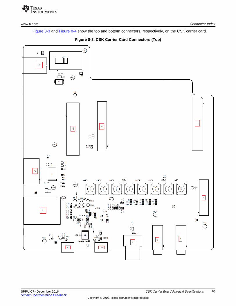
www.ti.com Connector Index
65SPRUIC7–December 2016Submit Documentation Feedback
Copyright © 2016, Texas Instruments Incorporated
CSK Carrier Board Physical Specifications
Figure 8-3 and Figure 8-4 show the top and bottom connectors, respectively, on the CSK carrier card.
Figure 8-3. CSK Carrier Card Connectors (Top)
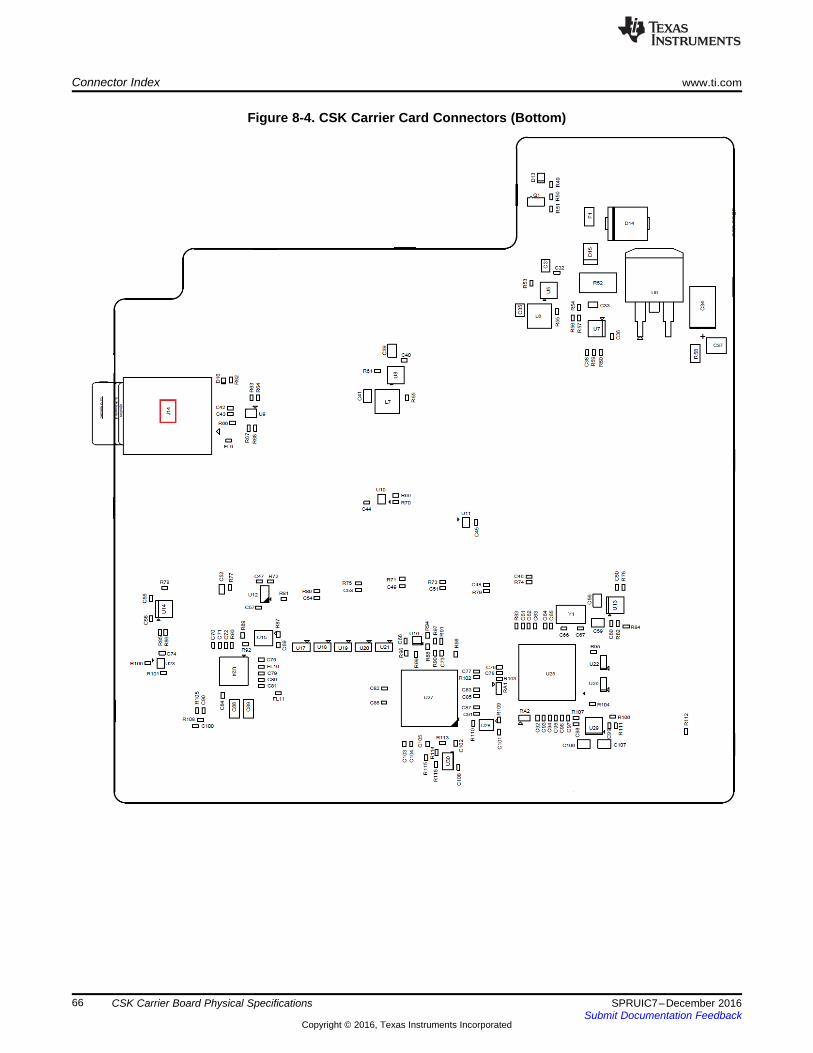
Connector Index www.ti.com
66 SPRUIC7–December 2016Submit Documentation Feedback
Copyright © 2016, Texas Instruments Incorporated
CSK Carrier Board Physical Specifications
Figure 8-4. CSK Carrier Card Connectors (Bottom)
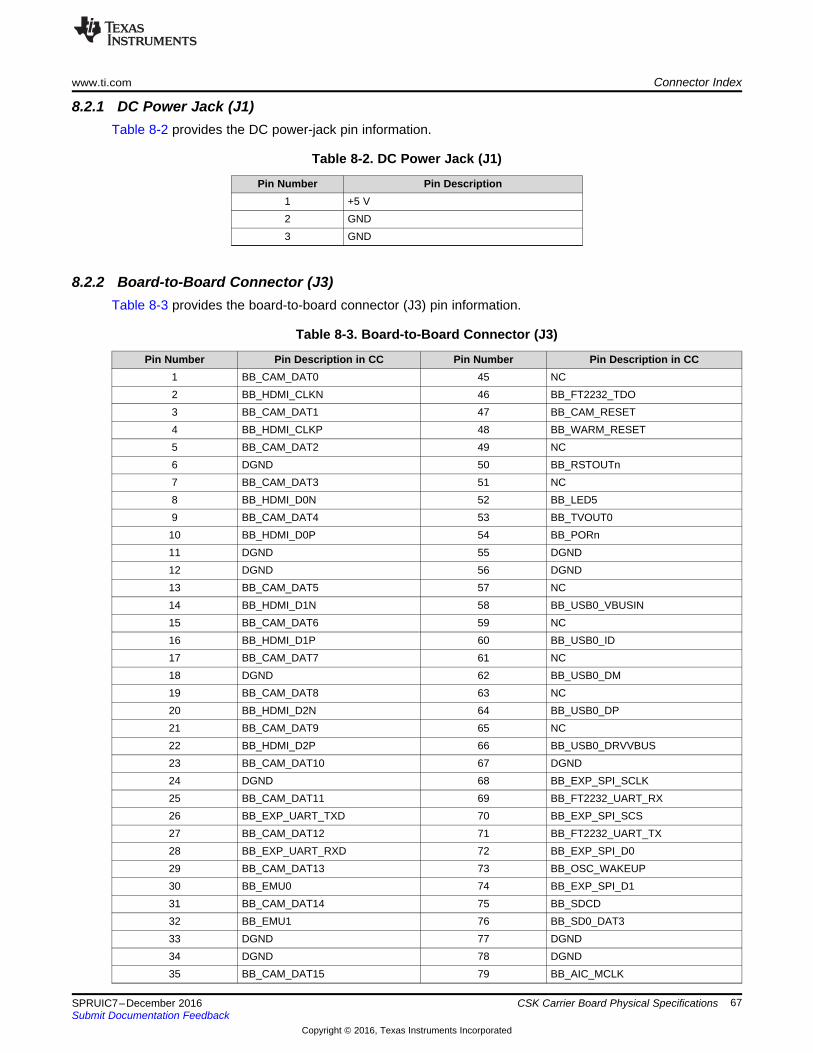
www.ti.com Connector Index
67SPRUIC7–December 2016Submit Documentation Feedback
Copyright © 2016, Texas Instruments Incorporated
CSK Carrier Board Physical Specifications
8.2.1 DC Power Jack (J1)Table 8-2 provides the DC power-jack pin information.
Table 8-2. DC Power Jack (J1)
Pin Number Pin Description1 +5 V2 GND3 GND
8.2.2 Board-to-Board Connector (J3)Table 8-3 provides the board-to-board connector (J3) pin information.
Table 8-3. Board-to-Board Connector (J3)
Pin Number Pin Description in CC Pin Number Pin Description in CC1 BB_CAM_DAT0 45 NC2 BB_HDMI_CLKN 46 BB_FT2232_TDO3 BB_CAM_DAT1 47 BB_CAM_RESET4 BB_HDMI_CLKP 48 BB_WARM_RESET5 BB_CAM_DAT2 49 NC6 DGND 50 BB_RSTOUTn7 BB_CAM_DAT3 51 NC8 BB_HDMI_D0N 52 BB_LED59 BB_CAM_DAT4 53 BB_TVOUT010 BB_HDMI_D0P 54 BB_PORn11 DGND 55 DGND12 DGND 56 DGND13 BB_CAM_DAT5 57 NC14 BB_HDMI_D1N 58 BB_USB0_VBUSIN15 BB_CAM_DAT6 59 NC16 BB_HDMI_D1P 60 BB_USB0_ID17 BB_CAM_DAT7 61 NC18 DGND 62 BB_USB0_DM19 BB_CAM_DAT8 63 NC20 BB_HDMI_D2N 64 BB_USB0_DP21 BB_CAM_DAT9 65 NC22 BB_HDMI_D2P 66 BB_USB0_DRVVBUS23 BB_CAM_DAT10 67 DGND24 DGND 68 BB_EXP_SPI_SCLK25 BB_CAM_DAT11 69 BB_FT2232_UART_RX26 BB_EXP_UART_TXD 70 BB_EXP_SPI_SCS27 BB_CAM_DAT12 71 BB_FT2232_UART_TX28 BB_EXP_UART_RXD 72 BB_EXP_SPI_D029 BB_CAM_DAT13 73 BB_OSC_WAKEUP30 BB_EMU0 74 BB_EXP_SPI_D131 BB_CAM_DAT14 75 BB_SDCD32 BB_EMU1 76 BB_SD0_DAT333 DGND 77 DGND34 DGND 78 DGND35 BB_CAM_DAT15 79 BB_AIC_MCLK
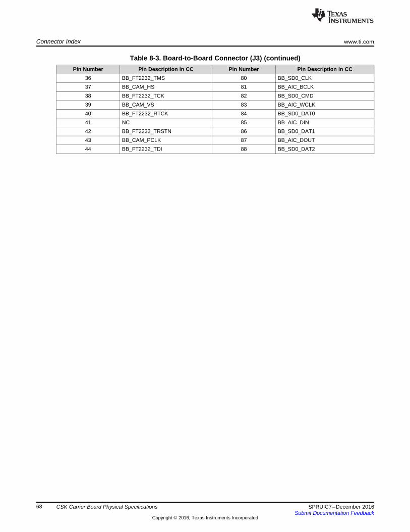
Connector Index www.ti.com
68 SPRUIC7–December 2016Submit Documentation Feedback
Copyright © 2016, Texas Instruments Incorporated
CSK Carrier Board Physical Specifications
Table 8-3. Board-to-Board Connector (J3) (continued)Pin Number Pin Description in CC Pin Number Pin Description in CC
36 BB_FT2232_TMS 80 BB_SD0_CLK37 BB_CAM_HS 81 BB_AIC_BCLK38 BB_FT2232_TCK 82 BB_SD0_CMD39 BB_CAM_VS 83 BB_AIC_WCLK40 BB_FT2232_RTCK 84 BB_SD0_DAT041 NC 85 BB_AIC_DIN42 BB_FT2232_TRSTN 86 BB_SD0_DAT143 BB_CAM_PCLK 87 BB_AIC_DOUT44 BB_FT2232_TDI 88 BB_SD0_DAT2
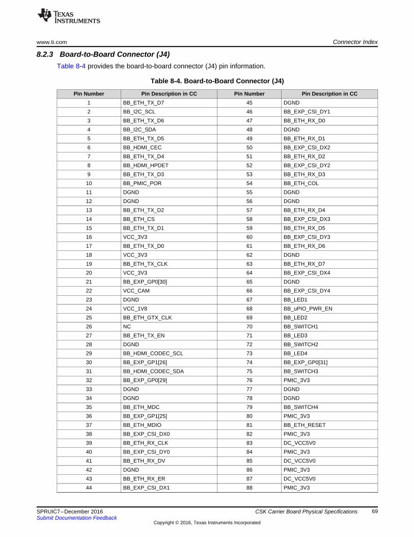
www.ti.com Connector Index
69SPRUIC7–December 2016Submit Documentation Feedback
Copyright © 2016, Texas Instruments Incorporated
CSK Carrier Board Physical Specifications
8.2.3 Board-to-Board Connector (J4)Table 8-4 provides the board-to-board connector (J4) pin information.
Table 8-4. Board-to-Board Connector (J4)
Pin Number Pin Description in CC Pin Number Pin Description in CC1 BB_ETH_TX_D7 45 DGND2 BB_I2C_SCL 46 BB_EXP_CSI_DY13 BB_ETH_TX_D6 47 BB_ETH_RX_D04 BB_I2C_SDA 48 DGND5 BB_ETH_TX_D5 49 BB_ETH_RX_D16 BB_HDMI_CEC 50 BB_EXP_CSI_DX27 BB_ETH_TX_D4 51 BB_ETH_RX_D28 BB_HDMI_HPDET 52 BB_EXP_CSI_DY29 BB_ETH_TX_D3 53 BB_ETH_RX_D310 BB_PMIC_POR 54 BB_ETH_COL11 DGND 55 DGND12 DGND 56 DGND13 BB_ETH_TX_D2 57 BB_ETH_RX_D414 BB_ETH_CS 58 BB_EXP_CSI_DX315 BB_ETH_TX_D1 59 BB_ETH_RX_D516 VCC_3V3 60 BB_EXP_CSI_DY317 BB_ETH_TX_D0 61 BB_ETH_RX_D618 VCC_3V3 62 DGND19 BB_ETH_TX_CLK 63 BB_ETH_RX_D720 VCC_3V3 64 BB_EXP_CSI_DX421 BB_EXP_GP0[30] 65 DGND22 VCC_CAM 66 BB_EXP_CSI_DY423 DGND 67 BB_LED124 VCC_1V8 68 BB_uPIO_PWR_EN25 BB_ETH_GTX_CLK 69 BB_LED226 NC 70 BB_SWITCH127 BB_ETH_TX_EN 71 BB_LED328 DGND 72 BB_SWITCH229 BB_HDMI_CODEC_SCL 73 BB_LED430 BB_EXP_GP1[26] 74 BB_EXP_GP0[31]31 BB_HDMI_CODEC_SDA 75 BB_SWITCH332 BB_EXP_GP0[29] 76 PMIC_3V333 DGND 77 DGND34 DGND 78 DGND35 BB_ETH_MDC 79 BB_SWITCH436 BB_EXP_GP1[25] 80 PMIC_3V337 BB_ETH_MDIO 81 BB_ETH_RESET38 BB_EXP_CSI_DX0 82 PMIC_3V339 BB_ETH_RX_CLK 83 DC_VCC5V040 BB_EXP_CSI_DY0 84 PMIC_3V341 BB_ETH_RX_DV 85 DC_VCC5V042 DGND 86 PMIC_3V343 BB_ETH_RX_ER 87 DC_VCC5V044 BB_EXP_CSI_DX1 88 PMIC_3V3
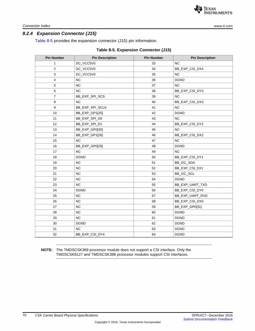
Connector Index www.ti.com
70 SPRUIC7–December 2016Submit Documentation Feedback
Copyright © 2016, Texas Instruments Incorporated
CSK Carrier Board Physical Specifications
8.2.4 Expansion Connector (J15)Table 8-5 provides the expansion connector (J15) pin information.
Table 8-5. Expansion Connector (J15)
Pin Number Pin Description Pin Number Pin Description1 DC_VCC5V0 33 NC2 DC_VCC5V0 34 BB_EXP_CSI_DX43 DC_VCC5V0 35 NC4 NC 36 DGND5 NC 37 NC6 NC 38 BB_EXP_CSI_DY37 BB_EXP_SPI_SCS 39 NC8 NC 40 BB_EXP_CSI_DX39 BB_EXP_SPI_SCLK 41 NC10 BB_EXP_GP1[25] 42 DGND11 BB_EXP_SPI_D0 43 NC12 BB_EXP_SPI_D1 44 BB_EXP_CSI_DY213 BB_EXP_GP0[30] 45 NC14 BB_EXP_GP1[26] 46 BB_EXP_CSI_DX215 NC 47 NC16 BB_EXP_GP0[29] 48 DGND17 NC 49 NC18 DGND 50 BB_EXP_CSI_DY119 NC 51 BB_I2C_SDA20 NC 52 BB_EXP_CSI_DX121 NC 53 BB_I2C_SCL22 NC 54 DGND23 NC 55 BB_EXP_UART_TXD24 DGND 56 BB_EXP_CSI_DY025 NC 57 BB_EXP_UART_RXD26 NC 58 BB_EXP_CSI_DX027 NC 59 BB_EXP_GP0[31]28 NC 60 DGND29 NC 61 DGND30 DGND 62 DGND31 NC 63 DGND32 BB_EXP_CSI_DY4 64 DGND
NOTE: The TMDSCSK369 processor module does not support a CSI interface. Only theTMDSCSK8127 and TMDSCSK388 processor modules support CSI interfaces.
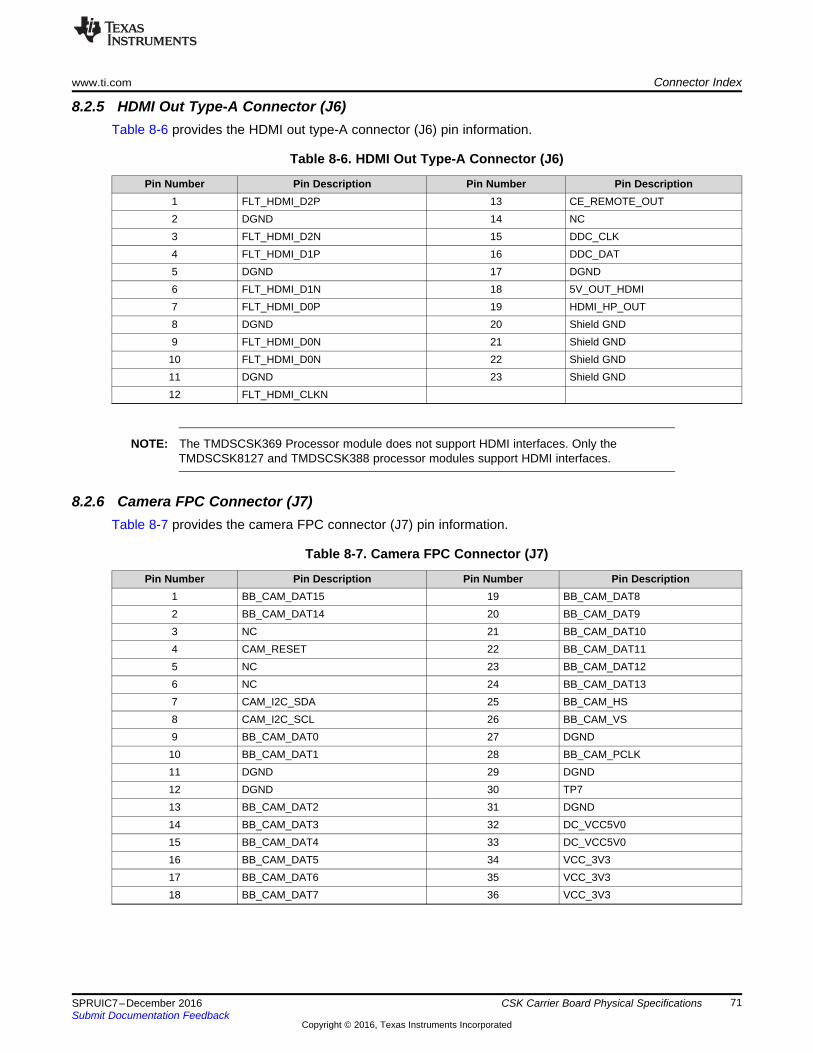
www.ti.com Connector Index
71SPRUIC7–December 2016Submit Documentation Feedback
Copyright © 2016, Texas Instruments Incorporated
CSK Carrier Board Physical Specifications
8.2.5 HDMI Out Type-A Connector (J6)Table 8-6 provides the HDMI out type-A connector (J6) pin information.
Table 8-6. HDMI Out Type-A Connector (J6)
Pin Number Pin Description Pin Number Pin Description1 FLT_HDMI_D2P 13 CE_REMOTE_OUT2 DGND 14 NC3 FLT_HDMI_D2N 15 DDC_CLK4 FLT_HDMI_D1P 16 DDC_DAT5 DGND 17 DGND6 FLT_HDMI_D1N 18 5V_OUT_HDMI7 FLT_HDMI_D0P 19 HDMI_HP_OUT8 DGND 20 Shield GND9 FLT_HDMI_D0N 21 Shield GND10 FLT_HDMI_D0N 22 Shield GND11 DGND 23 Shield GND12 FLT_HDMI_CLKN
NOTE: The TMDSCSK369 Processor module does not support HDMI interfaces. Only theTMDSCSK8127 and TMDSCSK388 processor modules support HDMI interfaces.
8.2.6 Camera FPC Connector (J7)Table 8-7 provides the camera FPC connector (J7) pin information.
Table 8-7. Camera FPC Connector (J7)
Pin Number Pin Description Pin Number Pin Description1 BB_CAM_DAT15 19 BB_CAM_DAT82 BB_CAM_DAT14 20 BB_CAM_DAT93 NC 21 BB_CAM_DAT104 CAM_RESET 22 BB_CAM_DAT115 NC 23 BB_CAM_DAT126 NC 24 BB_CAM_DAT137 CAM_I2C_SDA 25 BB_CAM_HS8 CAM_I2C_SCL 26 BB_CAM_VS9 BB_CAM_DAT0 27 DGND10 BB_CAM_DAT1 28 BB_CAM_PCLK11 DGND 29 DGND12 DGND 30 TP713 BB_CAM_DAT2 31 DGND14 BB_CAM_DAT3 32 DC_VCC5V015 BB_CAM_DAT4 33 DC_VCC5V016 BB_CAM_DAT5 34 VCC_3V317 BB_CAM_DAT6 35 VCC_3V318 BB_CAM_DAT7 36 VCC_3V3
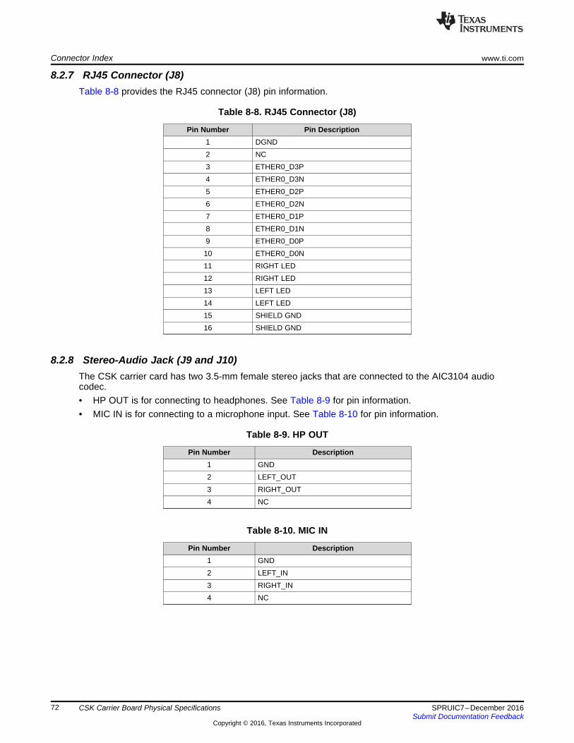
Connector Index www.ti.com
72 SPRUIC7–December 2016Submit Documentation Feedback
Copyright © 2016, Texas Instruments Incorporated
CSK Carrier Board Physical Specifications
8.2.7 RJ45 Connector (J8)Table 8-8 provides the RJ45 connector (J8) pin information.
Table 8-8. RJ45 Connector (J8)
Pin Number Pin Description1 DGND2 NC3 ETHER0_D3P4 ETHER0_D3N5 ETHER0_D2P6 ETHER0_D2N7 ETHER0_D1P8 ETHER0_D1N9 ETHER0_D0P10 ETHER0_D0N11 RIGHT LED12 RIGHT LED13 LEFT LED14 LEFT LED15 SHIELD GND16 SHIELD GND
8.2.8 Stereo-Audio Jack (J9 and J10)The CSK carrier card has two 3.5-mm female stereo jacks that are connected to the AIC3104 audiocodec.• HP OUT is for connecting to headphones. See Table 8-9 for pin information.• MIC IN is for connecting to a microphone input. See Table 8-10 for pin information.
Table 8-9. HP OUT
Pin Number Description1 GND2 LEFT_OUT3 RIGHT_OUT4 NC
Table 8-10. MIC IN
Pin Number Description1 GND2 LEFT_IN3 RIGHT_IN4 NC
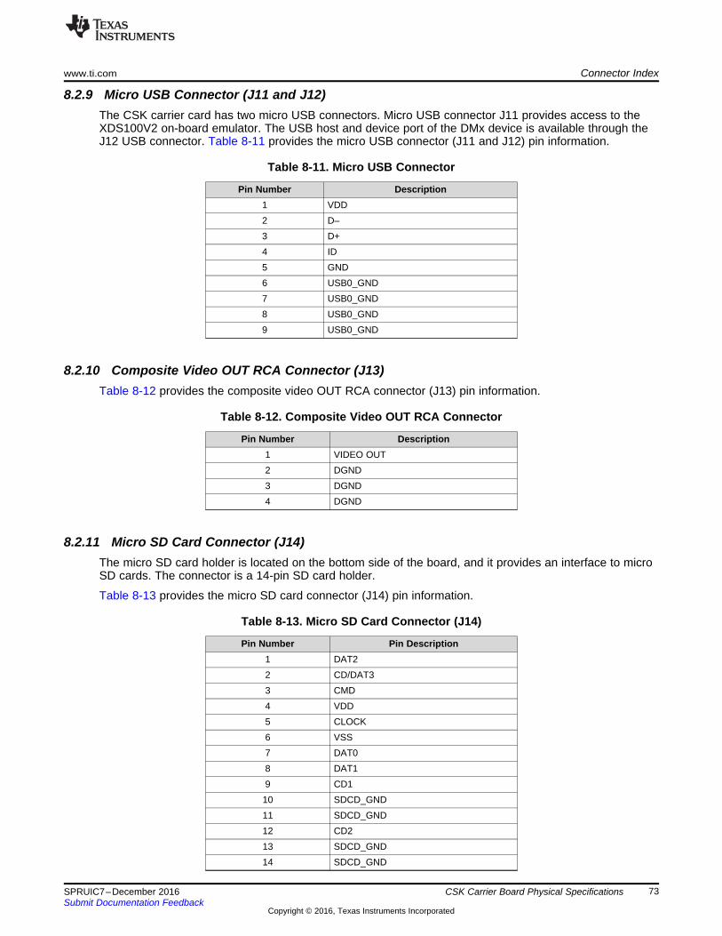
www.ti.com Connector Index
73SPRUIC7–December 2016Submit Documentation Feedback
Copyright © 2016, Texas Instruments Incorporated
CSK Carrier Board Physical Specifications
8.2.9 Micro USB Connector (J11 and J12)The CSK carrier card has two micro USB connectors. Micro USB connector J11 provides access to theXDS100V2 on-board emulator. The USB host and device port of the DMx device is available through theJ12 USB connector. Table 8-11 provides the micro USB connector (J11 and J12) pin information.
Table 8-11. Micro USB Connector
Pin Number Description1 VDD2 D–3 D+4 ID5 GND6 USB0_GND7 USB0_GND8 USB0_GND9 USB0_GND
8.2.10 Composite Video OUT RCA Connector (J13)Table 8-12 provides the composite video OUT RCA connector (J13) pin information.
Table 8-12. Composite Video OUT RCA Connector
Pin Number Description1 VIDEO OUT2 DGND3 DGND4 DGND
8.2.11 Micro SD Card Connector (J14)The micro SD card holder is located on the bottom side of the board, and it provides an interface to microSD cards. The connector is a 14-pin SD card holder.
Table 8-13 provides the micro SD card connector (J14) pin information.
Table 8-13. Micro SD Card Connector (J14)
Pin Number Pin Description1 DAT22 CD/DAT33 CMD4 VDD5 CLOCK6 VSS7 DAT08 DAT19 CD110 SDCD_GND11 SDCD_GND12 CD213 SDCD_GND14 SDCD_GND
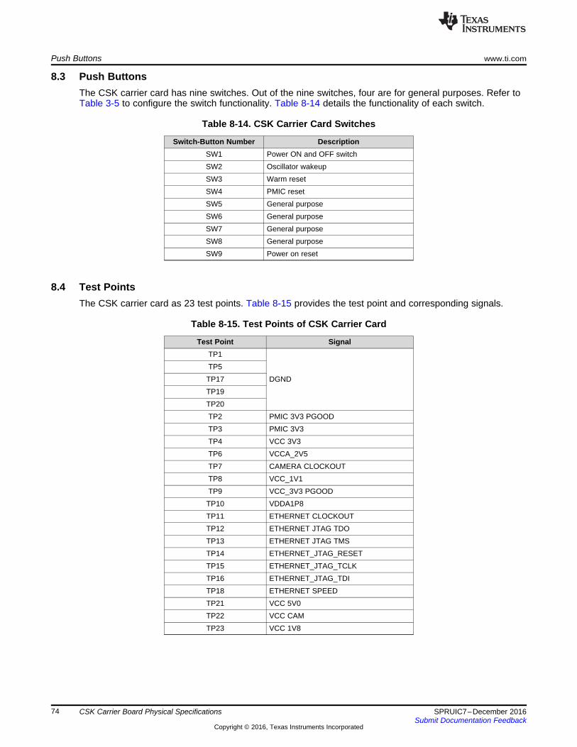
Push Buttons www.ti.com
74 SPRUIC7–December 2016Submit Documentation Feedback
Copyright © 2016, Texas Instruments Incorporated
CSK Carrier Board Physical Specifications
8.3 Push ButtonsThe CSK carrier card has nine switches. Out of the nine switches, four are for general purposes. Refer toTable 3-5 to configure the switch functionality. Table 8-14 details the functionality of each switch.
Table 8-14. CSK Carrier Card Switches
Switch-Button Number DescriptionSW1 Power ON and OFF switchSW2 Oscillator wakeupSW3 Warm resetSW4 PMIC resetSW5 General purposeSW6 General purposeSW7 General purposeSW8 General purposeSW9 Power on reset
8.4 Test PointsThe CSK carrier card as 23 test points. Table 8-15 provides the test point and corresponding signals.
Table 8-15. Test Points of CSK Carrier Card
Test Point SignalTP1
DGNDTP5TP17TP19TP20TP2 PMIC 3V3 PGOODTP3 PMIC 3V3TP4 VCC 3V3TP6 VCCA_2V5TP7 CAMERA CLOCKOUTTP8 VCC_1V1TP9 VCC_3V3 PGOODTP10 VDDA1P8TP11 ETHERNET CLOCKOUTTP12 ETHERNET JTAG TDOTP13 ETHERNET JTAG TMSTP14 ETHERNET_JTAG_RESETTP15 ETHERNET_JTAG_TCLKTP16 ETHERNET_JTAG_TDITP18 ETHERNET SPEEDTP21 VCC 5V0TP22 VCC CAMTP23 VCC 1V8
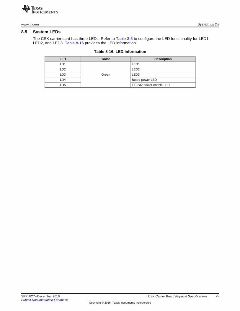
www.ti.com System LEDs
75SPRUIC7–December 2016Submit Documentation Feedback
Copyright © 2016, Texas Instruments Incorporated
CSK Carrier Board Physical Specifications
8.5 System LEDsThe CSK carrier card has three LEDs. Refer to Table 3-5 to configure the LED functionality for LED1,LED2, and LED3. Table 8-16 provides the LED information.
Table 8-16. LED Information
LED Color DescriptionLD1
Green
LED1LD2 LED2LD3 LED3LD4 Board-power LEDLD5 FT2232 power-enable LED
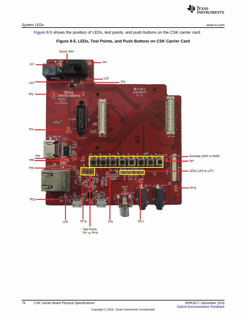
System LEDs www.ti.com
76 SPRUIC7–December 2016Submit Documentation Feedback
Copyright © 2016, Texas Instruments Incorporated
CSK Carrier Board Physical Specifications
Figure 8-5 shows the position of LEDs, test points, and push buttons on the CSK carrier card.
Figure 8-5. LEDs, Test Points, and Push Buttons on CSK Carrier Card
77SPRUIC7–December 2016Submit Documentation Feedback
Copyright © 2016, Texas Instruments Incorporated
CSK Carrier Card Power Requirements
Chapter 9SPRUIC7–December 2016
CSK Carrier Card Power Requirements
Topic ........................................................................................................................... Page
9.1 Power Distribution.............................................................................................. 789.2 Power Supply Calculation ................................................................................... 799.3 Power-up Sequence............................................................................................ 80
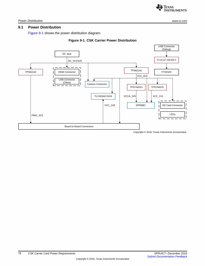
TPS62142
DC Jack
Board-to-Board Connectors
HDMI Connector
USB Connector (Client)
Camera Connector
TLV320AIC3104
TPS62142
TPS7A8101
DP83867 SD Card Connector
LEDs
FT2232H
TLV1117-33CDCY
USB Connector (Debug)
TPS7A8101
PMIC_3V3
DC_VCC5V0
VCC_1V8
VCCA_2V5 VCC_1V1
VCC_3V3
Copyright © 2016, Texas Instruments Incorporated
Power Distribution www.ti.com
78 SPRUIC7–December 2016Submit Documentation Feedback
Copyright © 2016, Texas Instruments Incorporated
CSK Carrier Card Power Requirements
9.1 Power DistributionFigure 9-1 shows the power distribution diagram.
Figure 9-1. CSK Carrier Power Distribution
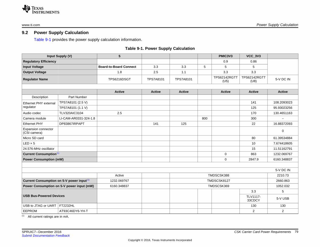
www.ti.com Power Supply Calculation
79SPRUIC7–December 2016Submit Documentation Feedback
Copyright © 2016, Texas Instruments Incorporated
CSK Carrier Card Power Requirements
9.2 Power Supply CalculationTable 9-1 provides the power supply calculation information.
(1) All current ratings are in mA.
Table 9-1. Power Supply Calculation
Input Supply (V) 5 PMIC3V3 VCC_3V3Regulatory Efficiency 0.9 0.86Input Voltage Board-to-Board Connect 3.3 3.3 5 5 5Output Voltage 1.8 2.5 1.1 3.3 3.3
Regulator Name TPS6216DSGT TPS7A8101 TPS7A8101 TPS62142RGTT(U5)
TPS62142RGTT(U8) 5-V DC IN
_Active Active Active Active Active Active
Description Part Number
Ethernet PHY externalregulator
TPS7A8101 (2.5 V) 141 108.2093023TPS7A8101 (1.1 V) 125 95.93023256
Audio codec TLV320AIC3104 2.5 170 130.4651163Camera module LI-CAM-AR0331-324-1.8 800 300 –Ethernet PHY DP83867IRPAPT 141 125 22 16.88372093Expansion connector(CSI camera) 0
Micro SD card 80 61.39534884LED × 5 10 7.67441860524.576-MHz oscillator 15 11.51162791Current Consumption (1) 0 863 1232.069767Power Consumption (mW) 0 2847.9 6160.348837_
5-V DC INActive TMDSCSK388 2210.73
Current Consumption on 5-V power input (1) 1232.069767 TMDSCSK8127 2660.863Power Consumption on 5-V power input (mW) 6160.348837 TMDSCSK369 1052.032
USB Bus-Powered Devices3.3 5
TLV1117-33CDCY 5-V USB
USB to JTAG or UART FT2232HL 130 130EEPROM AT93C46DY6-YH-T 2 2
PMIC_3V3
BB_uPIO_PWER_EN
VCC_3V3
VCCA_2V5
VCC_1V1
30 ms
3.3 V
5.0 V
3.3 V
2.5 V
1.1 V
5.0 V
DC_VCC5V0
Power-up Sequence www.ti.com
80 SPRUIC7–December 2016Submit Documentation Feedback
Copyright © 2016, Texas Instruments Incorporated
CSK Carrier Card Power Requirements
9.3 Power-up SequenceFigure 9-2 shows the power sequencing for the CSK carrier card.
Figure 9-2. Power-up Sequence
IMPORTANT NOTICE FOR TI DESIGN INFORMATION AND RESOURCES
Texas Instruments Incorporated (‘TI”) technical, application or other design advice, services or information, including, but not limited to,reference designs and materials relating to evaluation modules, (collectively, “TI Resources”) are intended to assist designers who aredeveloping applications that incorporate TI products; by downloading, accessing or using any particular TI Resource in any way, you(individually or, if you are acting on behalf of a company, your company) agree to use it solely for this purpose and subject to the terms ofthis Notice.TI’s provision of TI Resources does not expand or otherwise alter TI’s applicable published warranties or warranty disclaimers for TIproducts, and no additional obligations or liabilities arise from TI providing such TI Resources. TI reserves the right to make corrections,enhancements, improvements and other changes to its TI Resources.You understand and agree that you remain responsible for using your independent analysis, evaluation and judgment in designing yourapplications and that you have full and exclusive responsibility to assure the safety of your applications and compliance of your applications(and of all TI products used in or for your applications) with all applicable regulations, laws and other applicable requirements. Yourepresent that, with respect to your applications, you have all the necessary expertise to create and implement safeguards that (1)anticipate dangerous consequences of failures, (2) monitor failures and their consequences, and (3) lessen the likelihood of failures thatmight cause harm and take appropriate actions. You agree that prior to using or distributing any applications that include TI products, youwill thoroughly test such applications and the functionality of such TI products as used in such applications. TI has not conducted anytesting other than that specifically described in the published documentation for a particular TI Resource.You are authorized to use, copy and modify any individual TI Resource only in connection with the development of applications that includethe TI product(s) identified in such TI Resource. NO OTHER LICENSE, EXPRESS OR IMPLIED, BY ESTOPPEL OR OTHERWISE TOANY OTHER TI INTELLECTUAL PROPERTY RIGHT, AND NO LICENSE TO ANY TECHNOLOGY OR INTELLECTUAL PROPERTYRIGHT OF TI OR ANY THIRD PARTY IS GRANTED HEREIN, including but not limited to any patent right, copyright, mask work right, orother intellectual property right relating to any combination, machine, or process in which TI products or services are used. Informationregarding or referencing third-party products or services does not constitute a license to use such products or services, or a warranty orendorsement thereof. Use of TI Resources may require a license from a third party under the patents or other intellectual property of thethird party, or a license from TI under the patents or other intellectual property of TI.TI RESOURCES ARE PROVIDED “AS IS” AND WITH ALL FAULTS. TI DISCLAIMS ALL OTHER WARRANTIES ORREPRESENTATIONS, EXPRESS OR IMPLIED, REGARDING TI RESOURCES OR USE THEREOF, INCLUDING BUT NOT LIMITED TOACCURACY OR COMPLETENESS, TITLE, ANY EPIDEMIC FAILURE WARRANTY AND ANY IMPLIED WARRANTIES OFMERCHANTABILITY, FITNESS FOR A PARTICULAR PURPOSE, AND NON-INFRINGEMENT OF ANY THIRD PARTY INTELLECTUALPROPERTY RIGHTS.TI SHALL NOT BE LIABLE FOR AND SHALL NOT DEFEND OR INDEMNIFY YOU AGAINST ANY CLAIM, INCLUDING BUT NOTLIMITED TO ANY INFRINGEMENT CLAIM THAT RELATES TO OR IS BASED ON ANY COMBINATION OF PRODUCTS EVEN IFDESCRIBED IN TI RESOURCES OR OTHERWISE. IN NO EVENT SHALL TI BE LIABLE FOR ANY ACTUAL, DIRECT, SPECIAL,COLLATERAL, INDIRECT, PUNITIVE, INCIDENTAL, CONSEQUENTIAL OR EXEMPLARY DAMAGES IN CONNECTION WITH ORARISING OUT OF TI RESOURCES OR USE THEREOF, AND REGARDLESS OF WHETHER TI HAS BEEN ADVISED OF THEPOSSIBILITY OF SUCH DAMAGES.You agree to fully indemnify TI and its representatives against any damages, costs, losses, and/or liabilities arising out of your non-compliance with the terms and provisions of this Notice.This Notice applies to TI Resources. Additional terms apply to the use and purchase of certain types of materials, TI products and services.These include; without limitation, TI’s standard terms for semiconductor products http://www.ti.com/sc/docs/stdterms.htm), evaluationmodules, and samples (http://www.ti.com/sc/docs/sampterms.htm).
Mailing Address: Texas Instruments, Post Office Box 655303, Dallas, Texas 75265Copyright © 2017, Texas Instruments Incorporated