Embed Size (px)
Citation preview

Product
Folder
Order
Now
Technical
Documents
Tools &
Software
Support &Community
An IMPORTANT NOTICE at the end of this data sheet addresses availability, warranty, changes, use in safety-critical applications,intellectual property matters and other important disclaimers. PRODUCTION DATA.
DLP3310DLPS077B –JUNE 2016–REVISED JANUARY 2018
DLP3310 0.33 1080p DMD
1
1 Features1• 0.33-Inch (8.47-mm) Diagonal Micromirror Array
– Displays Full-HD 1920 × 1080 Pixels on theScreen
– 5.4-µm Micromirror Pitch– 17° Micromirror Tilt (Relative to Flat Surface)– Side Illumination for Optimal Efficiency and
Optical Engine Size– Polarization Independent Aluminum
Micromirror Surface• 32-Bit SubLVDS Input Data Bus• Dedicated DLPC3437 Display Controller and
DLPA3000 PMIC/LED Driver for ReliableOperation
2 Applications• Mobile Smart TVs• Screenless TVs• Gaming Displays• Digital Signage• Wearable Displays• Pico Projectors• Interactive Displays• Ultra Mobile Displays• Smart Home Displays• Virtual Assistant
3 DescriptionThe DLP3310 digital micromirror device (DMD) is adigitally controlled micro-opto-electromechanicalsystem (MOEMS) spatial light modulator (SLM).When coupled to an appropriate optical system, theDLP3310 DMD displays a very crisp and high qualityimage or video. DLP3310 is part of the chipsetcomprising of the DLP3310 DMD, DLPC3437 displaycontroller, and DLPA3000 PMIC/LED driver. Thecompact physical size of the DLP3310 coupled withthe controller and the PMIC/LED driver provides acomplete system solution that enables small formfactor, low power, and high resolution full-HDdisplays.
Device Information(1)
PART NUMBER PACKAGE BODY SIZE (NOM)
DLP3310 FQM (92) 19.25 mm × 7.2 mm
(1) For all available packages, see the orderable addendum atthe end of the data sheet.
Simplified Schematic
2
DLP3310DLPS077B –JUNE 2016–REVISED JANUARY 2018 www.ti.com
Product Folder Links: DLP3310
Submit Documentation Feedback Copyright © 2016–2018, Texas Instruments Incorporated
Table of Contents1 Features .................................................................. 12 Applications ........................................................... 13 Description ............................................................. 14 Revision History..................................................... 25 Pin Configuration and Functions ......................... 36 Specifications......................................................... 7
6.1 Absolute Maximum Ratings ..................................... 76.2 Storage Conditions.................................................... 76.3 ESD Ratings.............................................................. 86.4 Recommended Operating Conditions....................... 86.5 Thermal Information ................................................ 106.6 Electrical Characteristics......................................... 106.7 Timing Requirements .............................................. 116.8 Switching Characteristics ....................................... 166.9 System Mounting Interface Loads .......................... 166.10 Micromirror Array Physical Characteristics ........... 176.11 Micromirror Array Optical Characteristics ............. 186.12 Window Characteristics......................................... 196.13 Chipset Component Usage Specification ............. 19
7 Detailed Description ............................................ 207.1 Overview ................................................................. 207.2 Functional Block Diagram ....................................... 207.3 Feature Description................................................. 21
7.4 Device Functional Modes........................................ 217.5 Optical Interface and System Image Quality
Considerations ......................................................... 217.6 Micromirror Array Temperature Calculation............ 227.7 Micromirror Landed-On/Landed-Off Duty Cycle .... 23
8 Application and Implementation ........................ 288.1 Application Information............................................ 288.2 Typical Application .................................................. 29
9 Power Supply Recommendations ...................... 319.1 Power Supply Power-Up Procedure ...................... 319.2 Power Supply Power-Down Procedure .................. 319.3 Power Supply Sequencing Requirements .............. 32
10 Layout................................................................... 3410.1 Layout Guidelines ................................................. 3410.2 Layout Example .................................................... 34
11 Device and Documentation Support ................. 3511.1 Device Support...................................................... 3511.2 Related Links ........................................................ 3511.3 Community Resources.......................................... 3511.4 Trademarks ........................................................... 3611.5 Electrostatic Discharge Caution............................ 3611.6 Glossary ................................................................ 36
12 Mechanical, Packaging, and OrderableInformation ........................................................... 36
4 Revision History
Changes from Revision A (January 2017) to Revision B Page
• Removed the ± sign before 17° in Features........................................................................................................................... 1• Removed trace lengths of power supplies VBIAS, VOFFSET, and VRESET from Pin Functions - Connector Pins........................ 4• Updated MIN values for VDD and VDDI from 1.7 to 1.65 in Recommended Operating Conditions ......................................... 8• ILLVIS changed from TBD to Thermally Limited in Recommended Operating Conditions ..................................................... 9
Changes from Original (June 2016) to Revision A Page
• Updated list in Applications section........................................................................................................................................ 1• ILLVIS changed to TBD in Recommended Operating Conditions ........................................................................................... 9• Changed electrical characteristics values from TBD in Electrical Characteristics .............................................................. 10• Changed measured values for Capacitance under Electrical Characteristics .................................................................... 11• Included mechanical load values in System Mounting Interface Loads .............................................................................. 16

12 4 6 8
3 5 7 1718
1920
2122
2324
ABCDEFGH
3
DLP3310www.ti.com DLPS077B –JUNE 2016–REVISED JANUARY 2018
Product Folder Links: DLP3310
Submit Documentation FeedbackCopyright © 2016–2018, Texas Instruments Incorporated
(1) Low speed interface is LPSDR and adheres to the Electrical Characteristics and AC/DC Operating Conditions table in JEDEC StandardNo. 209B, Low Power Double Data Rate (LPDDR). See JESD209B.
(2) Net trace lengths inside the package:Relative dielectric constant for the FQM ceramic package is 9.8.Propagation speed = 11.8 / sqrt (9.8) = 3.769 in/ns.Propagation delay = 0.265 ns/inch = 265 ps/in = 10.43 ps/mm.
5 Pin Configuration and Functions
FQM Package92-Pin CLGABottom View
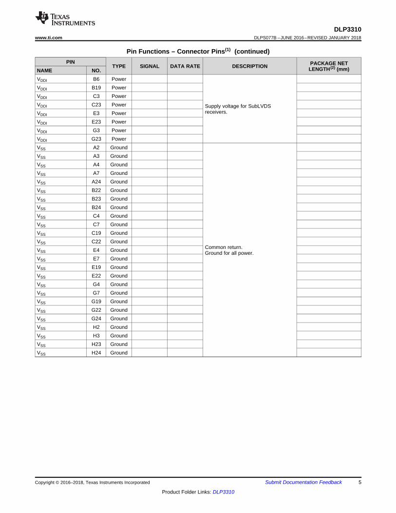
Pin Functions – Connector Pins (1)
PINTYPE SIGNAL DATA RATE DESCRIPTION PACKAGE NET
LENGTH (2) (mm)NAME NO.DATA INPUTSD_AN(0) C6 I SubLVDS Double Data, Negative 2.83D_AN(1) D7 I SubLVDS Double Data, Negative 4.00D_AN(2) D5 I SubLVDS Double Data, Negative 1.97D_AN(3) F7 I SubLVDS Double Data, Negative 4.03D_AN(4) F5 I SubLVDS Double Data, Negative 1.90D_AN(5) G6 I SubLVDS Double Data, Negative 3.08D_AN(6) H5 I SubLVDS Double Data, Negative 2.23D_AN(7) H7 I SubLVDS Double Data, Negative 3.88D_AP(0) C5 I SubLVDS Double Data, Positive 2.72D_AP(1) D6 I SubLVDS Double Data, Positive 3.89D_AP(2) D4 I SubLVDS Double Data, Positive 1.87D_AP(3) F6 I SubLVDS Double Data, Positive 3.93D_AP(4) F4 I SubLVDS Double Data, Positive 1.79D_AP(5) G5 I SubLVDS Double Data, Positive 2.97D_AP(6) H4 I SubLVDS Double Data, Positive 2.12D_AP(7) H6 I SubLVDS Double Data, Positive 3.78D_BN(0) C20 I SubLVDS Double Data, Negative 2.23D_BN(1) D19 I SubLVDS Double Data, Negative 3.27D_BN(2) D21 I SubLVDS Double Data, Negative 1.27D_BN(3) F19 I SubLVDS Double Data, Negative 3.52D_BN(4) F21 I SubLVDS Double Data, Negative 1.34D_BN(5) G20 I SubLVDS Double Data, Negative 2.55D_BN(6) H21 I SubLVDS Double Data, Negative 1.71D_BN(7) H19 I SubLVDS Double Data, Negative 3.37D_BP(0) C21 I SubLVDS Double Data, Positive 2.13
4
DLP3310DLPS077B –JUNE 2016–REVISED JANUARY 2018 www.ti.com
Product Folder Links: DLP3310
Submit Documentation Feedback Copyright © 2016–2018, Texas Instruments Incorporated
Pin Functions – Connector Pins(1) (continued)PIN
TYPE SIGNAL DATA RATE DESCRIPTION PACKAGE NETLENGTH (2) (mm)NAME NO.
(3) The following power supplies are all required to operate the DMD: VDD, VDDI, VOFFSET, VBIAS, VRESET. All VSS connections are alsorequired.
D_BP(1) D20 I SubLVDS Double Data, Positive 3.16D_BP(2) D22 I SubLVDS Double Data, Positive 1.17D_BP(3) F20 I SubLVDS Double Data, Positive 3.42D_BP(4) F22 I SubLVDS Double Data, Positive 1.23D_BP(5) G21 I SubLVDS Double Data, Positive 2.44D_BP(6) H22 I SubLVDS Double Data, Positive 1.61D_BP(7) H20 I SubLVDS Double Data, Positive 3.27DCLK_AN E6 I SubLVDS Double Clock, Negative 2.56DCLK_AP E5 I SubLVDS Double Clock, Positive 2.46DCLK_BN E20 I SubLVDS Double Clock, Negative 2.05DCLK_BP E21 I SubLVDS Double Clock, Positive 1.95CONTROL INPUTSLS_WDATA B3 I LPSDR (1) Single Write data for low speed interface. 1.78LS_CLK B5 I LPSDR Single Clock for low-speed interface. 1.78
DMD_DEN_ARSTZ B2 I LPSDR
Asynchronous reset DMD signal. Alow signal places the DMD in reset. Ahigh signal releases the DMD fromreset and places it in active mode.
0.85
LS_RDATA_A B7 O LPSDR Single Read data for low-speed interface. 4.19LS_RDATA_B B4 O LPSDR Single Read data for low-speed interface. 2.18POWERVBIAS
(3) A6 Power Supply voltage for positive bias levelat micromirrors.VBIAS
(3) A22 PowerVOFFSET
(3) B21 Power Supply voltage for HVCMOS corelogic. Supply voltage for stepped highlevel at micromirror addresselectrodes.Supply voltage for offset level atmicromirrors.
VOFFSET(3) G2 Power
VRESET A5 Power Supply voltage for negative reset levelat micromirrors.VRESET A23 Power
VDD(3) C2 Power
Supply voltage for LVCMOS corelogic. Supply voltage for LPSDRinputs.Supply voltage for normal high level atmicromirror address electrodes.
VDD A19 PowerVDD A20 PowerVDD A21 PowerVDD B20 PowerVDD C2 PowerVDD D2 PowerVDD D3 PowerVDD D23 PowerVDD E2 PowerVDD F2 PowerVDD F3 PowerVDD F23 Power
5
DLP3310www.ti.com DLPS077B –JUNE 2016–REVISED JANUARY 2018
Product Folder Links: DLP3310
Submit Documentation FeedbackCopyright © 2016–2018, Texas Instruments Incorporated
Pin Functions – Connector Pins(1) (continued)PIN
TYPE SIGNAL DATA RATE DESCRIPTION PACKAGE NETLENGTH (2) (mm)NAME NO.
VDDI B6 Power
Supply voltage for SubLVDSreceivers.
VDDI B19 PowerVDDI C3 PowerVDDI C23 PowerVDDI E3 PowerVDDI E23 PowerVDDI G3 PowerVDDI G23 PowerVSS A2 Ground
Common return.Ground for all power.
VSS A3 GroundVSS A4 GroundVSS A7 GroundVSS A24 GroundVSS B22 GroundVSS B23 GroundVSS B24 GroundVSS C4 GroundVSS C7 GroundVSS C19 GroundVSS C22 GroundVSS E4 GroundVSS E7 GroundVSS E19 GroundVSS E22 GroundVSS G4 GroundVSS G7 GroundVSS G19 GroundVSS G22 GroundVSS G24 GroundVSS H2 GroundVSS H3 GroundVSS H23 GroundVSS H24 Ground

6
DLP3310DLPS077B –JUNE 2016–REVISED JANUARY 2018 www.ti.com
Product Folder Links: DLP3310
Submit Documentation Feedback Copyright © 2016–2018, Texas Instruments Incorporated
Pin Functions – Test PadsNUMBER SYSTEM BOARD
A1 Do not connectA17 Do not connectA18 Do not connectB8 Do not connectB17 Do not connectB18 Do not connectC8 Do not connect
7
DLP3310www.ti.com DLPS077B –JUNE 2016–REVISED JANUARY 2018
Product Folder Links: DLP3310
Submit Documentation FeedbackCopyright © 2016–2018, Texas Instruments Incorporated
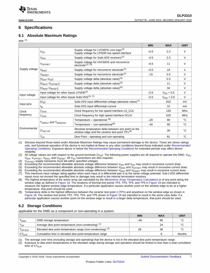
(1) Stresses beyond those listed under Absolute Maximum Ratings may cause permanent damage to the device. These are stress ratingsonly, and functional operation of the device is not implied at these or any other conditions beyond those indicated under RecommendedOperating Conditions. Exposure above or below the Recommended Operating Conditions for extended periods may affect devicereliability.
(2) All voltage values are with respect to the ground terminals (VSS). The following power supplies are all required to operate the DMD: VDD,VDDI, VOFFSET, VBIAS, and VRESET. All VSS connections are also required.
(3) VOFFSET supply transients must fall within specified voltages.(4) Exceeding the recommended allowable absolute voltage difference between VDDI and VDD may result in excessive current draw.(5) Exceeding the recommended allowable absolute voltage difference between VBIAS and VOFFSET may result in excessive current draw.(6) Exceeding the recommended allowable absolute voltage difference between VBIAS and VRESET may result in excessive current draw.(7) This maximum input voltage rating applies when each input of a differential pair is at the same voltage potential. Sub-LVDS differential
inputs must not exceed the specified limit or damage may result to the internal termination resistors.(8) The highest temperature of the active array (as calculated by the Micromirror Array Temperature Calculation) or of any point along the
window edge as defined in Figure 18. The locations of thermal test points TP2, TP3, TP4, and TP5 in Figure 18 are intended tomeasure the highest window edge temperature. If a particular application causes another point on the window edge to be at a highertemperature, that point should be used.
(9) Temperature delta is the highest difference between the ceramic test point 1 (TP1) and anywhere on the window edge as shown inFigure 18. The window test points TP2, TP3, TP4, and TP5 shown in Figure 18 are intended to result in the worst case delta. If aparticular application causes another point on the window edge to result in a larger delta temperature, that point should be used.
6 Specifications
6.1 Absolute Maximum Ratingssee (1)
MIN MAX UNIT
Supply voltage
VDDSupply voltage for LVCMOS core logic (2)
Supply voltage for LPSDR low speed interface –0.5 2.3 V
VDDI Supply voltage for SubLVDS receivers (2) –0.5 2.3 V
VOFFSETSupply voltage for HVCMOS and micromirrorelectrode (2) (3) –0.5 11 V
VBIAS Supply voltage for micromirror electrode (2) –0.5 19 VVRESET Supply voltage for micromirror electrode (2) –15 0.5 V|VDDI–VDD| Supply voltage delta (absolute value) (4) 0.3 V|VBIAS–VOFFSET| Supply voltage delta (absolute value) (5) 11 V|VBIAS–VRESET| Supply voltage delta (absolute value) (6) 34 V
Input voltageInput voltage for other inputs LPSDR (2) –0.5 VDD + 0.5 VInput voltage for other inputs SubLVDS (2) (7) –0.5 VDDI + 0.5 V
Input pins|VID| SubLVDS input differential voltage (absolute value) (7) 810 mVIID SubLVDS input differential current 10 mA
Clockfrequency
ƒclock Clock frequency for low speed interface LS_CLK 130 MHzƒclock Clock frequency for high speed interface DCLK 620 MHz
Environmental
TARRAY and TWINDOWTemperature – operational (8) –20 90 °CTemperature – non-operational (8) –40 90 °C
|TDELTA| Absolute temperature delta between any point on thewindow edge and the ceramic test point TP1 (9) 30 °C
TDP Dew Point - operating and non-operating 81 °C
(1) The average over time (including storage and operating) that the device is not in the elevated dew point temperature range.(2) Exposure to dew point temperatures in the elevated range during storage and operation should be limited to less than a total cumulative
time of CTELR.
6.2 Storage Conditionsapplicable for the DMD as a component or non-operating in a system.
MIN MAX UNITTDMD DMD storage temperature –40 85 °CTDP Average dew point temperature (non-condensing) (1) 24 °CTDP-ELR Elevated dew point temperature range (non-condensing) (2) 28 36 °CCTELR Cumulative time in elevated dew point temperature range 6 Months
8
DLP3310DLPS077B –JUNE 2016–REVISED JANUARY 2018 www.ti.com
Product Folder Links: DLP3310
Submit Documentation Feedback Copyright © 2016–2018, Texas Instruments Incorporated
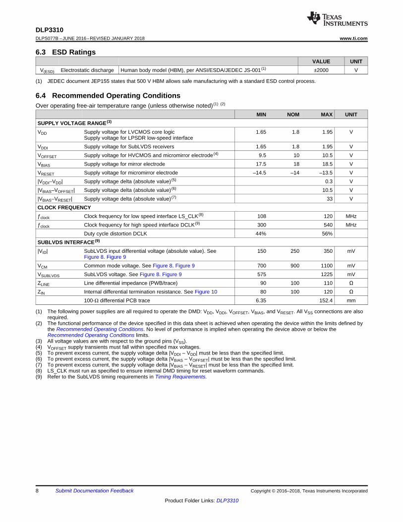
(1) JEDEC document JEP155 states that 500 V HBM allows safe manufacturing with a standard ESD control process.
6.3 ESD RatingsVALUE UNIT
V(ESD) Electrostatic discharge Human body model (HBM), per ANSI/ESDA/JEDEC JS-001 (1) ±2000 V
(1) The following power supplies are all required to operate the DMD: VDD, VDDI, VOFFSET, VBIAS, and VRESET. All VSS connections are alsorequired.
(2) The functional performance of the device specified in this data sheet is achieved when operating the device within the limits defined bythe Recommended Operating Conditions. No level of performance is implied when operating the device above or below theRecommended Operating Conditions limits.
(3) All voltage values are with respect to the ground pins (VSS).(4) VOFFSET supply transients must fall within specified max voltages.(5) To prevent excess current, the supply voltage delta |VDDI – VDD| must be less than the specified limit.(6) To prevent excess current, the supply voltage delta |VBIAS – VOFFSET| must be less than the specified limit.(7) To prevent excess current, the supply voltage delta |VBIAS – VRESET| must be less than the specified limit.(8) LS_CLK must run as specified to ensure internal DMD timing for reset waveform commands.(9) Refer to the SubLVDS timing requirements in Timing Requirements.
6.4 Recommended Operating ConditionsOver operating free-air temperature range (unless otherwise noted) (1) (2)
MIN NOM MAX UNITSUPPLY VOLTAGE RANGE (3)
VDD Supply voltage for LVCMOS core logicSupply voltage for LPSDR low-speed interface
1.65 1.8 1.95 V
VDDI Supply voltage for SubLVDS receivers 1.65 1.8 1.95 VVOFFSET Supply voltage for HVCMOS and micromirror electrode (4) 9.5 10 10.5 VVBIAS Supply voltage for mirror electrode 17.5 18 18.5 VVRESET Supply voltage for micromirror electrode –14.5 –14 –13.5 V|VDDI–VDD| Supply voltage delta (absolute value) (5) 0.3 V|VBIAS–VOFFSET| Supply voltage delta (absolute value) (6) 10.5 V|VBIAS–VRESET| Supply voltage delta (absolute value) (7) 33 VCLOCK FREQUENCYƒclock Clock frequency for low speed interface LS_CLK (8) 108 120 MHzƒclock Clock frequency for high speed interface DCLK (9) 300 540 MHz
Duty cycle distortion DCLK 44% 56%SUBLVDS INTERFACE (9)
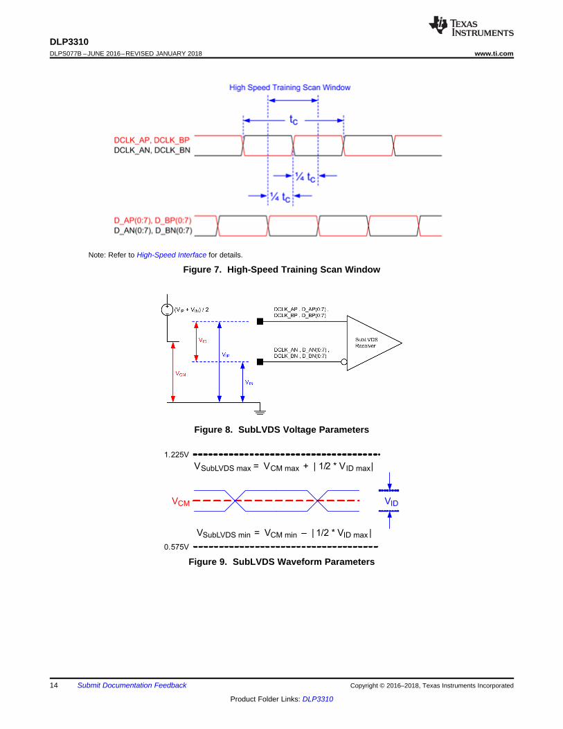
|VID| SubLVDS input differential voltage (absolute value). SeeFigure 8. Figure 9
150 250 350 mV
VCM Common mode voltage. See Figure 8. Figure 9 700 900 1100 mVVSUBLVDS SubLVDS voltage. See Figure 8. Figure 9 575 1225 mVZLINE Line differential impedance (PWB/trace) 90 100 110 ΩZIN Internal differential termination resistance. See Figure 10 80 100 120 Ω
100-Ω differential PCB trace 6.35 152.4 mm

Micromirror Landed Duty Cycle
Ope
ration
al (°
C)
0/100 5/95 10/90 15/85 20/80 25/75 30/70 35/65 40/60 45/5530
40
50
60
70
80
D001
50/50100/0 95/5 90/10 85/15 80/20 75/25 70/30 65/35 60/40 55/45
Max R
ecom
me
nd
ed
Arr
ay
Tem
pe
ratu
re–
9
DLP3310www.ti.com DLPS077B –JUNE 2016–REVISED JANUARY 2018
Product Folder Links: DLP3310
Submit Documentation FeedbackCopyright © 2016–2018, Texas Instruments Incorporated
Recommended Operating Conditions (continued)Over operating free-air temperature range (unless otherwise noted)(1) (2)
MIN NOM MAX UNIT
(10) Simultaneous exposure of the DMD to the maximum Recommended Operating Conditions for temperature and UV illumination willreduce device lifetime.
(11) The array temperature cannot be measured directly and must be computed analytically from the temperature measured at test point 1(TP1) shown in Figure 18 and the package thermal resistance using Micromirror Array Temperature Calculation.
(12) Per Figure 1, the maximum operational array temperature should be derated based on the micromirror landed duty cycle that the DMDexperiences in the end application. Refer to Micromirror Landed-On/Landed-Off Duty Cycle for a definition of micromirror landed dutycycle.
(13) Long-term is defined as the useful life of the device.(14) Short-term is the total cumulative time over the useful life of the device.(15) The locations of thermal test points TP2, TP3, TP4, and TP5 shown in Figure 18 are intended to measure the highest window edge
temperature. For most applications, the locations shown are representative of the highest window edge temperature. If a particularapplication causes additional points on the window edge to be at a higher temperature, test points should be added to those locations.
(16) The maximum marginal ray angle of the incoming illumination light at any point in the micromirror array, including Pond of Micromirrors(POM), should not exceed 55 degrees from the normal to the device array plane. The device window aperture has not necessarily beendesigned to allow incoming light at higher maximum angles to pass to the micromirrors, and the device performance has not been testednor qualified at angles exceeding this. Illumination light exceeding this angle outside the micromirror array (including POM) willcontribute to thermal limitations described in this document, and may negatively affect lifetime.
(17) Temperature delta is the highest difference between the ceramic test point 1 (TP1) and anywhere on the window edge shown inFigure 18. The window test points TP2, TP3, TP4, and TP5 shown in Figure 18 are intended to result in the worst case deltatemperature. If a particular application causes another point on the window edge to result in a larger delta temperature, that point shouldbe used.
(18) The average over time (including storage and operating) that the device is not in the elevated dew point temperature range.(19) Exposure to dew point temperatures in the elevated range during storage and operation should be limited to less than a total cumulative
time of CTELR.
ENVIRONMENTALTARRAY Array temperature – long-term operational (10) (11) (12) (13) 0 40 to 70 (12) °C
Array temperature – short-term operational, 25 hr max (11) (14) –20 –10 °CArray temperature – short-term operational, 500 hr max (11) (14) –10 0 °CArray temperature – short-term operational, 500 hr max (11) (14) 70 75 °C
TWINDOW Window temperature – operational (15) (16) 90 °C|TDELTA| Absolute temperature delta between any point on the window
edge and the ceramic test point TP1 (17)30 °C
TDP-AVG Average dew point temperature, non-condensing (18) 24 °CTDP-ELR Elevated dew point temperature range, non-condensing (19) 28 36 °CCTELR Cumulative time in elevated dew point temperature range. 6 MonthsILLUV Illumination wavelengths < 420 nm (10) 0.68 mW/cm2
ILLVIS Illumination wavelengths between 420 nm and 700 nm Thermally LimitedILLIR Illumination wavelengths > 700 nm 10 mW/cm2
ILLθ Illumination marginal ray angle (16) 55 degrees
Figure 1. Maximum Recommended Array Temperature – Derating Curve

10
DLP3310DLPS077B –JUNE 2016–REVISED JANUARY 2018 www.ti.com
Product Folder Links: DLP3310
Submit Documentation Feedback Copyright © 2016–2018, Texas Instruments Incorporated
(1) The DMD is designed to conduct absorbed and dissipated heat to the back of the package. The cooling system must be capable ofmaintaining the package within the temperature range specified in the Recommended Operating Conditions. The total heat load on theDMD is largely driven by the incident light absorbed by the active area; although other contributions include light energy absorbed by thewindow aperture and electrical power dissipation of the array. Optical systems should be designed to minimize the light energy fallingoutside the window clear aperture since any additional thermal load in this area can significantly degrade the reliability of the device.
6.5 Thermal Information
THERMAL METRIC (1)DLP3310
UNITFQM (LGA)92 PINS
Thermal resistance Active area to test point 1 (TP1) (1) 6.0 °C/W
(1) Device electrical characteristics are over Recommended Operating Conditions unless otherwise noted.(2) All voltage values are with respect to the ground pins (VSS).(3) To prevent excess current, the supply voltage delta |VDDI – VDD| must be less than the specified limit.(4) Supply power dissipation based on non–compressed commands and data.(5) To prevent excess current, the supply voltage delta |VBIAS – VOFFSET| must be less than the specified limit.(6) Supply power dissipation based on 3 global resets in 200 µs.(7) The following power supplies are all required to operate the DMD: VDD, VDDI, VOFFSET, VBIAS, VRESET. All VSS connections are also
required.(8) LPSDR specifications are for pins LS_CLK and LS_WDATA.(9) Low-speed interface is LPSDR and adheres to the Electrical Characteristics and AC/DC Operating Conditions table in JEDEC Standard
No. 209B, Low-Power Double Data Rate (LPDDR) JESD209B.
6.6 Electrical CharacteristicsOver operating free-air temperature range (unless otherwise noted) (1)
PARAMETER TEST CONDITIONS (2) MIN TYP MAX UNITCURRENT
IDD Supply current: VDD(3) (4) VDD = 1.95 V 135
mAVDD = 1.8 V 123.6
IDDI Supply current: VDDI(3) (4) VDDI = 1.95 V 35.34
mAVDD = 1.8 V 32
IOFFSET Supply current: VOFFSET(5) (6) VOFFSET = 10.5 V 2.55
mAVOFFSET = 10 V 2.5
IBIAS Supply current: VBIAS(5) (6) VBIAS = 18.5 V 1.25
mAVBIAS = 18 V 1.2
IRESET Supply current: VRESET(6) VRESET = –14.5 V –2.55
mAVRESET = –14 V –2.5
POWER (7)
PDD Supply power dissipation: VDD(3) (4) VDD = 1.95 V 263.25
mWVDD = 1.8 V 222.48
PDDI Supply power dissipation: VDDI(3) (4) VDDI = 1.95 V 68.91
mWVDD = 1.8 V 57.6
POFFSETSupply power dissipation: VOFFSET
(5)(6)
VOFFSET = 10.5 V 26.78mW
VOFFSET = 10 V 25
PBIAS Supply power dissipation: VBIAS(5) (6) VBIAS = 18.5 V 23.13
mWVBIAS = 18 V 21.6
PRESET Supply power dissipation: VRESET(6) VRESET = –14.5 V 36.98
mWVRESET = –14 V 35
PTOTAL Supply power dissipation: Total 361.68 419.05 mWLPSDR INPUT (8)
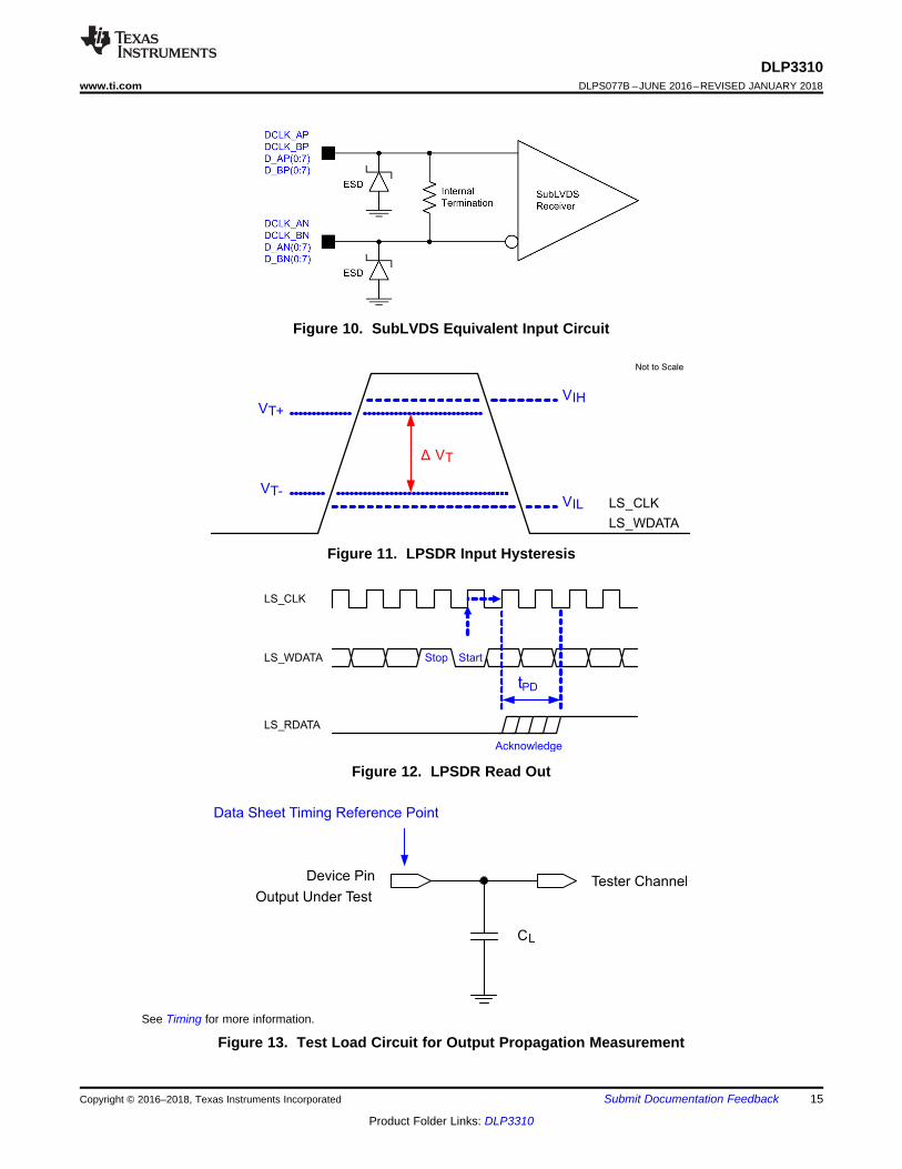
VIH(DC) DC input high voltage (9) 0.7 × VDD VDD + 0.3 VVIL(DC) DC input low voltage (9) –0.3 0.3 × VDD VVIH(AC) AC input high voltage (9) 0.8 × VDD VDD + 0.3 VVIL(AC) AC input low voltage (9) –0.3 0.2 × VDD V∆VT Hysteresis ( VT+ – VT– ) Figure 10 0.1 × VDD 0.4 × VDD V

11
DLP3310www.ti.com DLPS077B –JUNE 2016–REVISED JANUARY 2018
Product Folder Links: DLP3310
Submit Documentation FeedbackCopyright © 2016–2018, Texas Instruments Incorporated
Electrical Characteristics (continued)Over operating free-air temperature range (unless otherwise noted)(1)
PARAMETER TEST CONDITIONS (2) MIN TYP MAX UNIT
(10) LPSDR specification is for pin LS_RDATA.
IIL Low–level input current VDD = 1.95 V; VI = 0 V –100 nAIIH High–level input current VDD = 1.95 V; VI = 1.95 V 100 nALPSDR OUTPUT (10)
VOH DC output high voltage IOH = –2 mA 0.8 × VDD VVOL DC output low voltage IOL = 2 mA 0.2 × VDD VCAPACITANCE
CINInput capacitance LPSDR ƒ = 1 MHz 10 pFInput capacitance SubLVDS ƒ = 1 MHz 20 pF
COUT Output capacitance ƒ = 1 MHz 10 pFCRESET Reset group capacitance ƒ = 1 MHz; (768 × 344) micromirrors 400 500 pF
(1) Specification is for LS_CLK and LS_WDATA pins. Refer to LPSDR input rise slew rate and fall slew rate in Figure 3.(2) Specification is for DMD_DEN_ARSTZ pin. Refer to LPSDR input rise and fall slew rate in Figure 3.(3) Window time derating example: 0.5-V/ns slew rate increases the window time by 0.7 ns, from 3 to 3.7 ns.(4) Specification is for SubLVDS receiver time only and does not take into account commanding and latency after commanding.
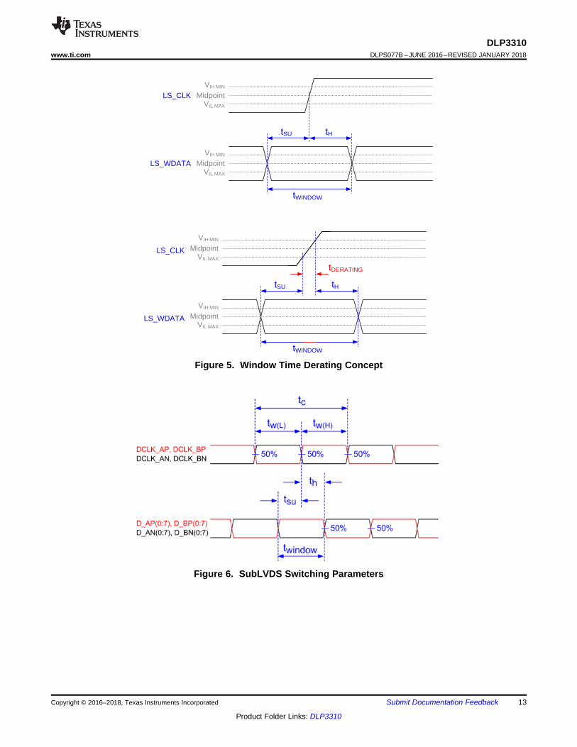
6.7 Timing RequirementsDevice electrical characteristics are over Recommended Operating Conditions unless otherwise noted.
MIN NOM MAX UNITLPSDRtr Rise slew rate (1) (30% to 80%) × VDD, See Figure 3 1 3 V/nstƒ Fall slew rate (1) (70% to 20%) × VDD, See Figure 3 1 3 V/nstr Rise slew rate (2) (20% to 80%) × VDD, See Figure 3 0.25 V/nstƒ Fall slew rate (2) (80% to 20%) × VDD, See Figure 3 0.25 V/nstc Cycle time LS_CLK, See Figure 2 7.7 8.3 nstW(H) Pulse duration LS_CLK
high 50% to 50% reference points, See Figure 2 3.1 ns
tW(L) Pulse duration LS_CLK low 50% to 50% reference points, See Figure 2 3.1 nstsu Setup time LS_WDATA valid before LS_CLK ↑, See
Figure 21.5 ns
t h Hold time LS_WDATA valid after LS_CLK ↑, SeeFigure 2
1.5 ns
tWINDOW Window time (1) (3) Setup time + Hold time, Figure 2 3 ns
tDERATING Window time derating (1) (3) For each 0.25 V/ns reduction in slew ratebelow 1 V/ns, See Figure 5
0.35 ns
SubLVDStr Rise slew rate 20% to 80% reference points, See Figure 4 0.7 1 V/nstƒ Fall slew rate 80% to 20% reference points, See Figure 4 0.7 1 V/nstc Cycle time DCLK See Figure 6 1.79 1.85 nstW(H) Pulse duration DCLK high 50% to 50% reference points, See Figure 6 0.79 nstW(L) Pulse duration DCLK low 50% to 50% reference points, See Figure 6 0.79 ns
tsu Setup time D(0:7) valid beforeDCLK ↑ or DCLK ↓, See Figure 6
t h Hold time D(0:7) valid afterDCLK ↑ or DCLK ↓, See Figure 6
tWINDOW Window time Setup time + Hold time, See Figure 6, Figure 7 0.3 nstLVDS-ENABLE+REFGEN
Power-up receiver (4) 2000 ns

0.0 * VDD
0.2 * VDD0.3 * VDD
0.7 * VDD0.8 * VDD
1.0 * VDD
VIH(AC)
VIH(DC)
VIL(DC)
VIL(AC)
tftr
LS_CLK, LS_WDATA
0.0 * VDD
0.2 * VDD
0.8 * VDD
1.0 * VDD
tftr
DMD_DEN_ARSTZ
LS_WDATA
LS_CLK
tw(H) tw(L)
tc
50%50%50%
50% 50%
th
tsu
twindow
12
DLP3310DLPS077B –JUNE 2016–REVISED JANUARY 2018 www.ti.com
Product Folder Links: DLP3310
Submit Documentation Feedback Copyright © 2016–2018, Texas Instruments Incorporated
Low-speed interface is LPSDR and adheres to the Electrical Characteristics and AC/DC Operating Conditions table inJEDEC Standard No. 209B, Low Power Double Data Rate (LPDDR) JESD209B.
Figure 2. LPSDR Switching Parameters
Figure 3. LPSDR Input Rise and Fall Slew Rate
Figure 4. SubLVDS Input Rise and Fall Slew Rate
LS_WDATA
LS_CLK
tSU tH
tWINDOW
VIH MIN
VIL MAX
Midpoint
VIH MIN
VIL MAX
Midpoint
tSU tH
tWINDOW
VIH MIN
VIL MAX
Midpoint
VIH MIN
VIL MAX
Midpoint
LS_WDATA
LS_CLK
tDERATING
13
DLP3310www.ti.com DLPS077B –JUNE 2016–REVISED JANUARY 2018
Product Folder Links: DLP3310
Submit Documentation FeedbackCopyright © 2016–2018, Texas Instruments Incorporated
Figure 5. Window Time Derating Concept
Figure 6. SubLVDS Switching Parameters
VCM VID
VSubLVDS max = VCM max + | 1/2 * VID max|
0.575V
1.225V
VSubLVDS min = VCM min – | 1/2 * VID max |
14
DLP3310DLPS077B –JUNE 2016–REVISED JANUARY 2018 www.ti.com
Product Folder Links: DLP3310
Submit Documentation Feedback Copyright © 2016–2018, Texas Instruments Incorporated
Note: Refer to High-Speed Interface for details.
Figure 7. High-Speed Training Scan Window
Figure 8. SubLVDS Voltage Parameters
Figure 9. SubLVDS Waveform Parameters
CL
Tester ChannelOutput Under Test
Data Sheet Timing Reference Point
Device Pin
Stop Start
LS_CLK
LS_WDATA
LS_RDATA
Acknowledge
tPD
VIH
Δ VT
VT+
VT-VIL
LS_WDATA
LS_CLK
Not to Scale
15
DLP3310www.ti.com DLPS077B –JUNE 2016–REVISED JANUARY 2018
Product Folder Links: DLP3310
Submit Documentation FeedbackCopyright © 2016–2018, Texas Instruments Incorporated
Figure 10. SubLVDS Equivalent Input Circuit
Figure 11. LPSDR Input Hysteresis
Figure 12. LPSDR Read Out
See Timing for more information.
Figure 13. Test Load Circuit for Output Propagation Measurement
Datum 'A' Areas(3 Place)
Datum 'E' Area(1 Place)
Thermal Interface Area
Electrical Interface Area
16
DLP3310DLPS077B –JUNE 2016–REVISED JANUARY 2018 www.ti.com
Product Folder Links: DLP3310
Submit Documentation Feedback Copyright © 2016–2018, Texas Instruments Incorporated
(1) Device electrical characteristics are over Recommended Operating Conditions unless otherwise noted.
6.8 Switching Characteristics (1)
Over operating free-air temperature range (unless otherwise noted).PARAMETER TEST CONDITIONS MIN TYP MAX UNIT
tPD
Output propagation, Clock to Q, risingedge of LS_CLK input to LS_RDATAoutput (See Figure 12).
CL = 5 pF 11.1 nsCL = 10 pF 11.3 nsCL = 85 pF 15 ns
Slew rate, LS_RDATA 0.5 V/nsOutput duty cycle distortion, LS_RDATA 40% 60%
(1) Uniformly distributed within area shown in Figure 14.
6.9 System Mounting Interface Loads
PARAMETER MIN NOM MAX UNITMaximum system mounting interface load to be applied to the:
• Thermal Interface Area (1) 60 N
• Clamping and Electrical Interface Area (1) 110 N
Figure 14. System Interface Loads

ε
ε
εε
17
DLP3310www.ti.com DLPS077B –JUNE 2016–REVISED JANUARY 2018
Product Folder Links: DLP3310
Submit Documentation FeedbackCopyright © 2016–2018, Texas Instruments Incorporated
(1) The structure and qualities of the border around the active array includes a band of partially functional micromirrors called the POM.These micromirrors are structurally and/or electrically prevented from tilting toward the bright or ON state, but still require an electricalbias to tilt toward OFF.
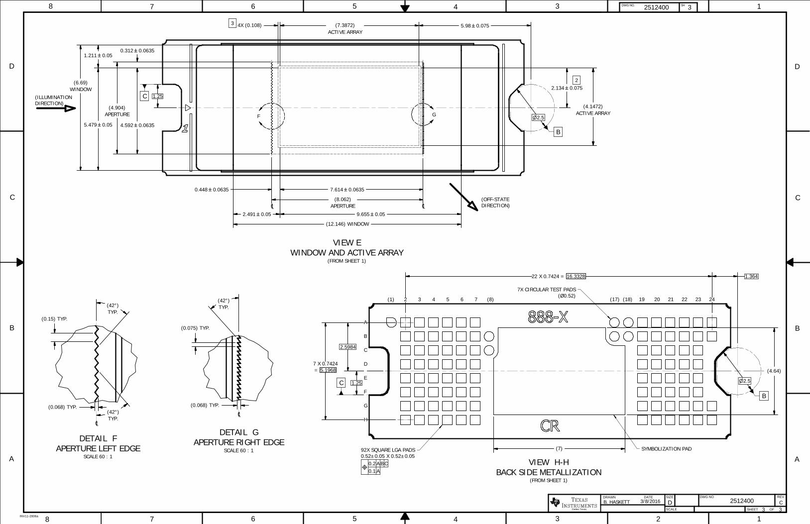
6.10 Micromirror Array Physical Characteristics
PARAMETER VALUE UNITNumber of active columns See Figure 15 1368 micromirrorsNumber of active rows See Figure 15 768 micromirrors
ε Micromirror (pixel) pitch See Figure 16 5.4 µmMicromirror active arraywidth Micromirror pitch × number of active columns; see Figure 15 7.387 mm
Micromirror active arrayheight Micromirror pitch × number of active rows; see Figure 15 4.147 mm
Micromirror active border Pond of micromirror (POM) (1) 20 micromirrors/side
Figure 15. Micromirror Array Physical Characteristics
Figure 16. Mirror (Pixel) Pitch

18
DLP3310DLPS077B –JUNE 2016–REVISED JANUARY 2018 www.ti.com
Product Folder Links: DLP3310
Submit Documentation Feedback Copyright © 2016–2018, Texas Instruments Incorporated
(1) Measured relative to the plane formed by the overall micromirror array.(2) Additional variation exists between the micromirror array and the package datums.(3) Represents the landed tilt angle variation relative to the nominal landed tilt angle.(4) Represents the variation that can occur between any two individual micromirrors, located on the same device or located on different
devices.(5) For some applications, it is critical to account for the micromirror tilt angle variation in the overall system optical design. With some
system optical designs, the micromirror tilt angle variation within a device may result in perceivable non-uniformities in the light fieldreflected from the micromirror array. With some system optical designs, the micromirror tilt angle variation between devices may result incolorimetry variations, system efficiency variations, or system contrast variations.
(6) When the micromirror array is landed (not parked), the tilt direction of each individual micromirror is dictated by the binary contents ofthe CMOS memory cell associated with each individual micromirror. A binary value of 1 results in a micromirror landing in the ON Statedirection. A binary value of 0 results in a micromirror landing in the OFF State direction.
(7) Micromirror tilt direction is measured as in a typical polar coordinate system: measuring counter-clockwise from a 0° reference which isaligned with the +X Cartesian axis.
(8) The time required for a micromirror to nominally transition from one landed state to the opposite landed state.(9) The minimum time between successive transitions of a micromirror.(10) An out-of-specification micromirror is defined as a micromirror that is unable to transition between the two landed states within the
specified Micromirror Switching Time.
6.11 Micromirror Array Optical Characteristics
PARAMETER TEST CONDITIONS MIN NOM MAX UNITMicromirror tilt angle DMD landed state (1) 17 degreeMicromirror tilt angle tolerance (2) (3) (4) (5) –1.4 1.4 degree
Micromirror tilt direction (6) (7) Landed ON state 180degree
Landed OFF state 270Micromirror crossover time (8) Typical Performance 1 3
µsMicromirror switching time (9) Typical Performance 10
Number of out-of-specificationmicromirrors (10)
Adjacent micromirrors 0micromirrors
Non-adjacent micromirrors 10
Figure 17. Landed Pixel Orientation and Tilt

19
DLP3310www.ti.com DLPS077B –JUNE 2016–REVISED JANUARY 2018
Product Folder Links: DLP3310
Submit Documentation FeedbackCopyright © 2016–2018, Texas Instruments Incorporated
(1) See Optical Interface and System Image Quality Considerations for more information.(2) See the package mechanical characteristics for details regarding the size and location of the window aperture.(3) The active area of the DLP3310 device is surrounded by an aperture on the inside of the DMD window surface that masks structures of
the DMD device assembly from normal view. The aperture is sized to anticipate several optical conditions. Overfill light illuminating thearea outside the active array can scatter and create adverse effects to the performance of an end application using the DMD. Theillumination optical system should be designed to limit light flux incident outside the active array to less than 10% of the average fluxlevel in the active area. Depending on the particular system's optical architecture and assembly tolerances, the amount of overfill light onthe outside of the active array may cause system performance degradation.
6.12 Window Characteristics
PARAMETER (1) MIN NOM MAX UNITWindow material Corning Eagle XGWindow refractive index at wavelength 546.1 nm 1.5119Window aperture (2) See (2)
Illumination overfill (3) See (3)
Window transmittance, single-passthrough both surfaces and glass
Minimum within the wavelength range420 to 680 nm. Applies to all angles 0°to 30° AOI.
97%
Window Transmittance, single-passthrough both surfaces and glass
Average over the wavelength range 420to 680 nm. Applies to all angles 30° to45° AOI.
97%
6.13 Chipset Component Usage Specification
NOTETI assumes no responsibility for image quality artifacts or DMD failures caused by opticalsystem operating conditions exceeding limits described previously.
The DLP3310 is a component of one or more DLP® chipsets. Reliable function and operation of the DLP3310requires that it be used in conjunction with the other components of the applicable DLP chipset, including thosecomponents that contain or implement TI DMD control technology. TI DMD control technology consists of the TItechnology and devices for operating or controlling a DLP DMD.
20
DLP3310DLPS077B –JUNE 2016–REVISED JANUARY 2018 www.ti.com
Product Folder Links: DLP3310
Submit Documentation Feedback Copyright © 2016–2018, Texas Instruments Incorporated
7 Detailed Description
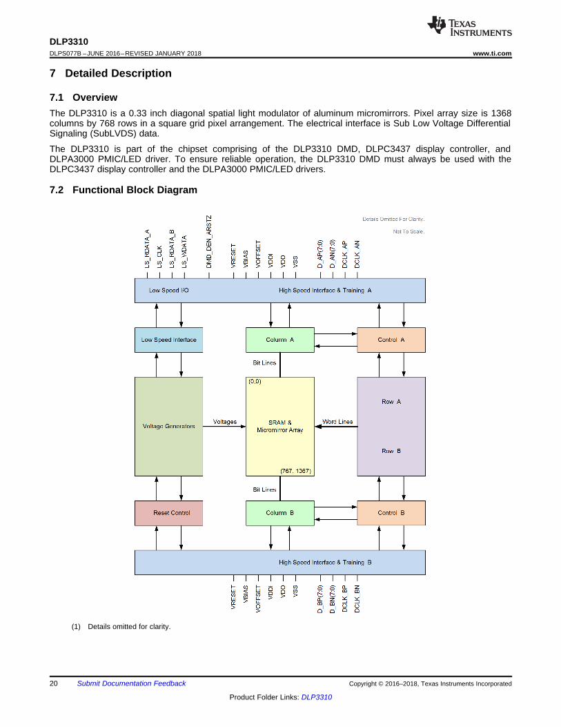
7.1 OverviewThe DLP3310 is a 0.33 inch diagonal spatial light modulator of aluminum micromirrors. Pixel array size is 1368columns by 768 rows in a square grid pixel arrangement. The electrical interface is Sub Low Voltage DifferentialSignaling (SubLVDS) data.
The DLP3310 is part of the chipset comprising of the DLP3310 DMD, DLPC3437 display controller, andDLPA3000 PMIC/LED driver. To ensure reliable operation, the DLP3310 DMD must always be used with theDLPC3437 display controller and the DLPA3000 PMIC/LED drivers.
7.2 Functional Block Diagram
(1) Details omitted for clarity.

21
DLP3310www.ti.com DLPS077B –JUNE 2016–REVISED JANUARY 2018
Product Folder Links: DLP3310
Submit Documentation FeedbackCopyright © 2016–2018, Texas Instruments Incorporated
7.3 Feature Description
7.3.1 Power InterfaceThe power management IC DLPA3000 contains 3 regulated DC supplies for the DMD reset circuitry: VBIAS,VRESET and VOFFSET, as well as the 2 regulated DC supplies for the DLPC3437 controller.
7.3.2 Low-Speed InterfaceThe Low Speed Interface handles instructions that configure the DMD and control reset operation. LS_CLK is thelow–speed clock, and LS_WDATA is the low speed data input.
7.3.3 High-Speed InterfaceThe purpose of the high-speed interface is to transfer pixel data rapidly and efficiently, making use of high speedDDR transfer and compression techniques to save power and time. The high-speed interface is composed ofdifferential SubLVDS receivers for inputs, with a dedicated clock.
7.3.4 TimingThe data sheet provides timing at the device pin. For output timing analysis, the tester pin electronics and itstransmission line effects must be taken into account. Figure 13 shows an equivalent test load circuit for theoutput under test. Timing reference loads are not intended as a precise representation of any particular systemenvironment or depiction of the actual load presented by a production test. System designers should use IBIS orother simulation tools to correlate the timing reference load to a system environment. The load capacitance valuestated is only for characterization and measurement of AC timing signals. This load capacitance value does notindicate the maximum load the device is capable of driving.
7.4 Device Functional ModesDMD functional modes are controlled by the DLPC3437 controller. See the DLPC3437 controller data sheet orcontact a TI applications engineer.
7.5 Optical Interface and System Image Quality ConsiderationsTI assumes no responsibility for end-equipment optical performance. Achieving the desired end-equipmentoptical performance involves making trade-offs between numerous component and system design parameters.Optimizing system optical performance and image quality strongly relate to optical system design parametertrades. Although it is not possible to anticipate every conceivable application, projector image quality and opticalperformance is contingent on compliance to the optical system operating conditions described in the followingsections.
7.5.1 Numerical Aperture and Stray Light ControlThe angle defined by the numerical aperture of the illumination and projection optics at the DMD optical areashould be the same. This angle should not exceed the nominal device micromirror tilt angle unless appropriateapertures are added in the illumination and/or projection pupils to block out flat-state and stray light from theprojection lens. The micromirror tilt angle defines DMD capability to separate the "ON" optical path from anyother light path, including undesirable flat-state specular reflections from the DMD window, DMD borderstructures, or other system surfaces near the DMD such as prism or lens surfaces. If the numerical apertureexceeds the micromirror tilt angle, or if the projection numerical aperture angle is more than two degrees largerthan the illumination numerical aperture angle (and vice versa), contrast degradation and objectionable artifactsin the display border and/or active area could occur.
7.5.2 Pupil MatchTI’s optical and image quality specifications assume that the exit pupil of the illumination optics is nominallycentered within 2° of the entrance pupil of the projection optics. Misalignment of pupils can create objectionableartifacts in the display’s border and/or active area, which may require additional system apertures to control,especially if the numerical aperture of the system exceeds the pixel tilt angle.

22
DLP3310DLPS077B –JUNE 2016–REVISED JANUARY 2018 www.ti.com
Product Folder Links: DLP3310
Submit Documentation Feedback Copyright © 2016–2018, Texas Instruments Incorporated
Optical Interface and System Image Quality Considerations (continued)7.5.3 Illumination OverfillThe active area of the device is surrounded by an aperture on the inside DMD window surface that masksstructures of the DMD chip assembly from normal view, and is sized to anticipate several optical operatingconditions. Overfill light illuminating the window aperture can create artifacts from the edge of the windowaperture opening and other surface anomalies that may be visible on the screen. The illumination optical systemshould be designed to limit light flux incident anywhere on the window aperture from exceeding approximately10% of the average flux level in the active area. Depending on the particular system’s optical architecture, overfilllight may have to be further reduced below the suggested 10% level in order to be acceptable.
7.6 Micromirror Array Temperature Calculation
Figure 18. DMD Thermal Test Points

23
DLP3310www.ti.com DLPS077B –JUNE 2016–REVISED JANUARY 2018
Product Folder Links: DLP3310
Submit Documentation FeedbackCopyright © 2016–2018, Texas Instruments Incorporated
Micromirror Array Temperature Calculation (continued)Micromirror array temperature cannot be measured directly, therefore it must be computed analytically frommeasurement points on the outside of the package, the package thermal resistance, the electrical power, and theillumination heat load. The relationship between array temperature and the reference ceramic temperature(thermal test TP1 in Figure 18) is provided by the following equations:
TARRAY = TCERAMIC + (QARRAY × RARRAY-TO-CERAMIC)QARRAY = QELECTRICAL + QILLUMINATION
where• TARRAY = computed array temperature (°C)• TCERAMIC = measured ceramic temperature (°C) (TP1 location)• RARRAY-TO-CERAMIC = thermal resistance of package specified in Thermal Information from array to ceramic TP1
(°C/Watt)• QARRAY = Total (electrical + absorbed) DMD power on the array (Watts)• QELECTRICAL = nominal electrical power• QILLUMINATION = (CL2W × SL)• CL2W = Conversion constant for screen lumens to power on DMD (Watts/Lumen)• SL = measured screen Lumens
The electrical power dissipation of the DMD is variable and depends on the voltages, data rates and operatingfrequencies. A nominal electrical power dissipation to use when calculating array temperature is 0.16 Watts. Theabsorbed power from the illumination source is variable and depends on the operating state of the micromirrorsand the intensity of the light source. The equations shown above are valid for a 1-Chip DMD system withprojection efficiency from the DMD to the screen of 87%.
The conversion constant CL2W is calculated to be 0.00266 W/lm based on array characteristics. It assumes aspectral efficiency of 300 lumens/Watt for the projected light and illumination distribution of 83.7% on the activearray, and 16.3% on the array border.
Sample calculations for typical projection application:CL2W = 0.00266 W/lmSL = 450 lmQELECTRICAL = 0.16 WTCERAMIC = 55.0°CQARRAY = 0.16 W + (0.00266 W/lm × 450 lm) = 1.36 WTARRAY = 55.0°C + (1.36 W × 6°C/W) = 63.2°C
7.7 Micromirror Landed-On/Landed-Off Duty Cycle
7.7.1 Definition of Micromirror Landed-On/Landed-Off Duty CycleThe micromirror landed-on/landed-off duty cycle (landed duty cycle) denotes the amount of time (as apercentage) that an individual micromirror is landed in the On state versus the amount of time the samemicromirror is landed in the Off state.
As an example, a landed duty cycle of 100/0 indicates that the referenced pixel is in the On state 100% of thetime (and in the Off state 0% of the time), whereas 0/100 would indicate that the pixel is in the Off state 100% ofthe time. Likewise, 50/50 indicates that the pixel is On 50% of the time and Off 50% of the time.
Note that when assessing landed duty cycle, the time spent switching from one state (ON or OFF) to the otherstate (OFF or ON) is considered negligible and is thus ignored.
Since a micromirror can only be landed in one state or the other (ON or OFF), the two numbers (percentages)always add to 100.
7.7.2 Landed Duty Cycle and Useful Life of the DMDKnowing the long-term average landed duty cycle (of the end product or application) is important becausesubjecting all (or a portion) of the DMD’s micromirror array (also called the active array) to an asymmetric landedduty cycle for a prolonged period of time can reduce the DMD’s usable life.

24
DLP3310DLPS077B –JUNE 2016–REVISED JANUARY 2018 www.ti.com
Product Folder Links: DLP3310
Submit Documentation Feedback Copyright © 2016–2018, Texas Instruments Incorporated
Micromirror Landed-On/Landed-Off Duty Cycle (continued)Note that it is the symmetry/asymmetry of the landed duty cycle that is of relevance. The symmetry of the landedduty cycle is determined by how close the two numbers (percentages) are to being equal. For example, a landedduty cycle of 50/50 is perfectly symmetrical whereas a landed duty cycle of 100/0 or 0/100 is perfectlyasymmetrical.

25
DLP3310www.ti.com DLPS077B –JUNE 2016–REVISED JANUARY 2018
Product Folder Links: DLP3310
Submit Documentation FeedbackCopyright © 2016–2018, Texas Instruments Incorporated
Micromirror Landed-On/Landed-Off Duty Cycle (continued)7.7.3 Landed Duty Cycle and Operational DMD TemperatureOperational DMD Temperature and Landed Duty Cycle interact to affect the DMD’s usable life, and thisinteraction can be exploited to reduce the impact that an asymmetrical Landed Duty Cycle has on the DMD’susable life. This is quantified in the de-rating curve shown in Figure 1. The importance of this curve is that:• All points along this curve represent the same usable life.• All points above this curve represent lower usable life (and the further away from the curve, the lower the
usable life).• All points below this curve represent higher usable life (and the further away from the curve, the higher the
usable life).
In practice, this curve specifies the Maximum Operating DMD Temperature that the DMD should be operated atfor a given long-term average Landed Duty Cycle.
7.7.4 Estimating the Long-Term Average Landed Duty Cycle of a Product or ApplicationDuring a given period of time, the Landed Duty Cycle of a given pixel follows from the image content beingdisplayed by that pixel.
For example, in the simplest case, when displaying pure-white on a given pixel for a given time period, that pixelwill experience a 100/0 Landed Duty Cycle during that time period. Likewise, when displaying pure-black, thepixel will experience a 0/100 Landed Duty Cycle.
Between the two extremes (ignoring for the moment color and any image processing that may be applied to anincoming image), the Landed Duty Cycle tracks one-to-one with the gray scale value, as shown in Table 1.
Table 1. Grayscale Value andLanded Duty Cycle
GrayscaleValue Landed Duty Cycle
0% 0/10010% 10/9020% 20/8030% 30/7040% 40/6050% 50/5060% 60/4070% 70/3080% 80/2090% 90/10100% 100/0
Accounting for color rendition (but still ignoring image processing) requires knowing both the color intensity (from0% to 100%) for each constituent primary color (red, green, and/or blue) for the given pixel as well as the colorcycle time for each primary color, where “color cycle time” is the total percentage of the frame time that a givenprimary must be displayed in order to achieve the desired white point.
During a given period of time, the landed duty cycle of a given pixel can be calculated as follows:Landed Duty Cycle = (Red_Cycle_% × Red_Scale_Value) + (Green_Cycle_% × Green_Scale_Value) +(Blue_Cycle_%×Blue_Scale_Value)
whereRed_Cycle_%, Green_Cycle_%, and Blue_Cycle_% represent the percentage of the frame time that Red, Green, andBlue are displayed (respectively) to achieve the desired white point. (1)
For example, assume that the red, green and blue color cycle times are 50%, 20%, and 30% respectively (inorder to achieve the desired white point), then the Landed Duty Cycle for various combinations of red, green,blue color intensities would be as shown in Table 2.

Input Level (%)
Out
put L
evel
(%
)
0 10 20 30 40 50 60 70 80 90 1000
10
20
30
40
50
60
70
80
90
100
D002
Gamma = 2.2
26
DLP3310DLPS077B –JUNE 2016–REVISED JANUARY 2018 www.ti.com
Product Folder Links: DLP3310
Submit Documentation Feedback Copyright © 2016–2018, Texas Instruments Incorporated
Table 2. Example Landed Duty Cycle for Full-ColorPixels
Red CyclePercentage
Green CyclePercentage
Blue CyclePercentage
50% 20% 30%
Red ScaleValue
Green ScaleValue
Blue ScaleValue
Landed DutyCycle
0% 0% 0% 0/100100% 0% 0% 50/50
0% 100% 0% 20/800% 0% 100% 30/70
12% 0% 0% 6/940% 35% 0% 7/930% 0% 60% 18/82
100% 100% 0% 70/300% 100% 100% 50/50
100% 0% 100% 80/2012% 35% 0% 13/870% 35% 60% 25/75
12% 0% 60% 24/76100% 100% 100% 100/0
The last factor to account for in estimating the Landed Duty Cycle is any applied image processing. Within theDLP Controller DLPC3437, the two functions which affect Landed Duty Cycle are Gamma and IntelliBright™.
Gamma is a power function of the form Output_Level = A × Input_LevelGamma, where A is a scaling factor that istypically set to 1.
In the DLPC3430/DLPC3435 controller, gamma is applied to the incoming image data on a pixel-by-pixel basis.A typical gamma factor is 2.2, which transforms the incoming data as shown in Figure 19.
Figure 19. Example of Gamma = 2.2

27
DLP3310www.ti.com DLPS077B –JUNE 2016–REVISED JANUARY 2018
Product Folder Links: DLP3310
Submit Documentation FeedbackCopyright © 2016–2018, Texas Instruments Incorporated
From Figure 19, if the gray scale value of a given input pixel is 40% (before gamma is applied), then gray scalevalue will be 13% after gamma is applied. Therefore, it can be seen that since gamma has a direct impactdisplayed gray scale level of a pixel, it also has a direct impact on the landed duty cycle of a pixel.
The IntelliBright algorithms content adaptive illumination control (CAIC) and local area brightness boost (LABB)also apply transform functions on the gray scale level of each pixel.
But while the amount of gamma applied to every pixel (of every frame) is constant (the exponent, gamma, isconstant), CAIC and LABB are both adaptive functions that can apply a different amounts of either boost orcompression to every pixel of every frame.
Consideration must also be given to any image processing which occurs before the DLPC3437 controller.
28
DLP3310DLPS077B –JUNE 2016–REVISED JANUARY 2018 www.ti.com
Product Folder Links: DLP3310
Submit Documentation Feedback Copyright © 2016–2018, Texas Instruments Incorporated
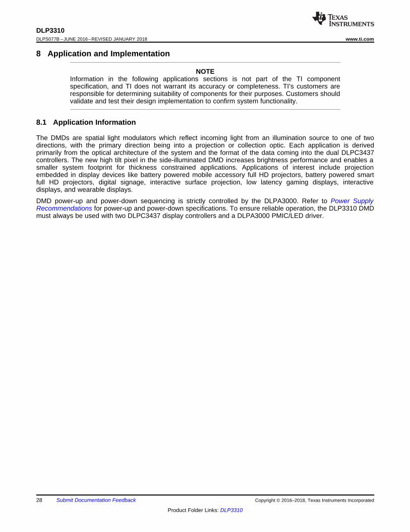
8 Application and Implementation
NOTEInformation in the following applications sections is not part of the TI componentspecification, and TI does not warrant its accuracy or completeness. TI’s customers areresponsible for determining suitability of components for their purposes. Customers shouldvalidate and test their design implementation to confirm system functionality.
8.1 Application Information
The DMDs are spatial light modulators which reflect incoming light from an illumination source to one of twodirections, with the primary direction being into a projection or collection optic. Each application is derivedprimarily from the optical architecture of the system and the format of the data coming into the dual DLPC3437controllers. The new high tilt pixel in the side-illuminated DMD increases brightness performance and enables asmaller system footprint for thickness constrained applications. Applications of interest include projectionembedded in display devices like battery powered mobile accessory full HD projectors, battery powered smartfull HD projectors, digital signage, interactive surface projection, low latency gaming displays, interactivedisplays, and wearable displays.
DMD power-up and power-down sequencing is strictly controlled by the DLPA3000. Refer to Power SupplyRecommendations for power-up and power-down specifications. To ensure reliable operation, the DLP3310 DMDmust always be used with two DLPC3437 display controllers and a DLPA3000 PMIC/LED driver.

Projector Module Electronics
SPI_0
PARKZ
VCC_FLSH
I2C_0
LED_SEL(2)
WVGADDR DMD
0.33 1080PDMD
RESETZ
PROJ_ON
CMP_OUT
INTZ Illumination
Optics3
VBIAS, VRST, VOFS
Thermistor
LABB
L3SYSPWR
1.1 VReg
L1
L2
VLED
BLUEGREEN
RED
CurrentSense
WPC
GPIO_8 (Normal Park) 1.8 V VSPI
PARKZ
SPI_1
Sub-LVDS DATALS CTRL & DATA
L41.8 VReg
DLPA3000
PAD Control 4
L5DCReg
3.3 V (to front-end chip)2.5 V (to front-end chip)
LDO#1LDO#2
Fan or a programmable DC supply
1.8 V for DMD and DLPC3437s
1.1 V for DLPC3437sVIN
Oscillator
eDRAM
DLPC3437
1.1 V VCOREVIO
SPI_0VCC_FLSH
FLASH, SDRAM
Keypad
PROJ_ONHDMI Receiver
Triple ADC
DC Supplies
Charger
BAT+ ±
6-20VDC
VDD
On/Off
HDMI
VGA
SD Card Reader, Video
Decoder, etc.
1.1V VCORE
VIO
eDRAM
DLPC3437
VCC_INTF
Parallel
3DR
I2C
28Parallel
3DR
HOST_IRQ
FPD-Link
1.0 V
1.8 V
VCOREVIO
SPIFlash
DDR3LI/FVCC_DDRFrame
Memory
FPGA
XC7Z020-1CLG484I4493
VCC_INTF
Parallel
3DRI2C_1I2C_1
GPIO_14-19
Image Sync
I2C_0I2C_1HOST_IRQ
I2C_0
RESETZ
INTZ
3D L/RGPIO_09
ACT_SYNC
ActuatorDriveCircuit
DAC_Data
DAC_CLK
FPGA_RDY
RESETZ
DSI I/F, CPU I/F, and BT656 I/F are not supported for dual ASIC.
Included in DLP® Chip Set
Non-TI components
DC_IN
Front-EndChip
- OSD- AutoLock - Scaler- uController
Flash
Sub-LVDS DATA
LS_RDATA
Flash
CMP_PWM
1.35 V
1.8 V
1.8 V
VCC_FLSH
29
DLP3310www.ti.com DLPS077B –JUNE 2016–REVISED JANUARY 2018
Product Folder Links: DLP3310
Submit Documentation FeedbackCopyright © 2016–2018, Texas Instruments Incorporated
8.2 Typical Application
A common application when using a DLP3310 DMD and two DLPC3437s is for creating a pico-projector that canbe used as an accessory to a smartphone, tablet or a laptop. The two DLPC3437s in the pico-projector receiveimages from the XC7Z020-1CLG484I4493 FPGA, which receives images from a multimedia front end within theproduct as shown in Figure 20.
Figure 20. Typical Application Diagram
8.2.1 Design Requirements
A pico-projector is created by using a DLP chip set comprised of a DLP3310 DMD, two DLPC3437 controllers, aXC7Z020-1CLG484I4493 FPGA, and a DLPA3000 PMIC/LED driver. The XC7Z020-1CLG484I4493 FPGA andDLPC3437 controllers do the digital image processing, the DLPA3000 provides the needed analog functions forthe projector, and the DLP3310 DMD is the display device for producing the projected image.
In addition to the three DLP chips in the chip set, other chips are needed. At a minimum a Flash part is neededto store the software and firmware to control the XC7Z020-1CLG484I4493 FPGA, and each of the DLPC3437controllers.
The illumination light that is applied to the DMD is typically from red, green, and blue LEDs. These are oftencontained in three separate packages, but sometimes more than one color of LED die may be in the samepackage to reduce the overall size of the pico-projector.
For connecting the XC7Z020-1CLG484I4493 FPGA to the multimedia front end for receiving images, either a 24-bit parallel interface can be used, or the dual FPD-Link interface can be used. An I2C interface should beconnected from the multimedia front end for sending commands to one of the DLPC3437 controllers forconfiguring the chipset for different features.

LED CURRENT (A)
RE
LAT
IVE
LU
MIN
AN
CE
LE
VE
L
0 0.5 1 1.5 2 2.5 3 3.5 4 4.5 5 5.5 60
0.1
0.2
0.3
0.4
0.5
0.6
0.7
0.8
0.9
1
D001
30
DLP3310DLPS077B –JUNE 2016–REVISED JANUARY 2018 www.ti.com
Product Folder Links: DLP3310
Submit Documentation Feedback Copyright © 2016–2018, Texas Instruments Incorporated
Typical Application (continued)8.2.2 Detailed Design Procedure
For connecting together the XC7Z020-1CLG484I4493 FPGA, the two DLPC3437 controllers, the DLPA3000, andthe DLP3310 DMD, see the reference design schematic. When a circuit board layout is created from thisschematic a very small circuit board is possible. An example small board layout is included in the referencedesign data base. Layout guidelines should be followed to achieve a reliable projector.
The optical engine that has the LED packages and the DMD mounted to it is typically supplied by an opticalOEM who specializes in designing optics for DLP projectors.
8.2.3 Application Curve
As the LED currents that are driven time-sequentially through the red, green, and blue LEDs are increased, thebrightness of the projector increases. This increase is somewhat non-linear, and the curve for typical whitescreen lumens changes with LED currents is as shown in Figure 21. For the LED currents shown, it’s assumedthat the same current amplitude is applied to the red, green, and blue LEDs.
Figure 21. Luminance vs Current

31
DLP3310www.ti.com DLPS077B –JUNE 2016–REVISED JANUARY 2018
Product Folder Links: DLP3310
Submit Documentation FeedbackCopyright © 2016–2018, Texas Instruments Incorporated
9 Power Supply RecommendationsThe following power supplies are all required to operate the DMD: VDD, VDDI, VOFFSET, VBIAS, and VRESET. All VSSconnections are also required. DMD power-up and power-down sequencing is strictly controlled by theDLPA3000 devices.
CAUTIONFor reliable operation of the DMD, the following power supply sequencingrequirements must be followed. Failure to adhere to the prescribed power-up andpower-down procedures may affect device reliability.
VDD, VDDI, VOFFSET, VBIAS, and VRESET power supplies have to be coordinated duringpower-up and power-down operations. Failure to meet any of the below requirementswill result in a significant reduction in the DMD’s reliability and lifetime. Refer toFigure 23. VSS must also be connected.
9.1 Power Supply Power-Up Procedure• During power-up, VDD and VDDI must always start and settle before VOFFSET, VBIAS, and VRESET voltages are
applied to the DMD.• During power-up, it is a strict requirement that the delta between VBIAS and VOFFSET must be within the
specified limit shown in Recommended Operating Conditions. Refer to Table 3 and the Layout Example forpower-up delay requirements.
• During power-up, the DMD’s LPSDR input pins shall not be driven high until after VDD and VDDI have settledat operating voltage.
• During power-up, there is no requirement for the relative timing of VRESET with respect to VOFFSET and VBIAS.Power supply slew rates during power-up are flexible, provided that the transient voltage levels follow therequirements listed previously and in Figure 22.
9.2 Power Supply Power-Down Procedure• Power-down sequence is the reverse order of the previous power-up sequence. VDD and VDDI must be
supplied until after VBIAS, VRESET, and VOFFSET are discharged to within 4 V of ground.• During power-down, it is not mandatory to stop driving VBIAS prior to VOFFSET, but it is a strict requirement that
the delta between VBIAS and VOFFSET must be within the specified limit shown in Recommended OperatingConditions (Refer to Note 2 for Figure 22).
• During power-down, the DMD’s LPSDR input pins must be less than VDDI, the specified limit shown inRecommended Operating Conditions.
• During power-down, there is no requirement for the relative timing of VRESET with respect to VOFFSET andVBIAS.
• Power supply slew rates during power-down are flexible, provided that the transient voltage levels follow therequirements listed previously and in Figure 22.
32
DLP3310DLPS077B –JUNE 2016–REVISED JANUARY 2018 www.ti.com
Product Folder Links: DLP3310
Submit Documentation Feedback Copyright © 2016–2018, Texas Instruments Incorporated
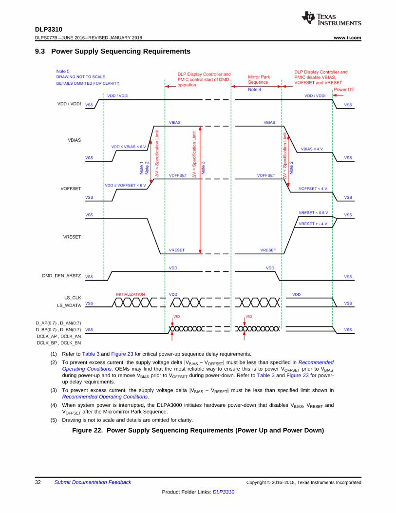
9.3 Power Supply Sequencing Requirements
(1) Refer to Table 3 and Figure 23 for critical power-up sequence delay requirements.(2) To prevent excess current, the supply voltage delta |VBIAS – VOFFSET| must be less than specified in Recommended
Operating Conditions. OEMs may find that the most reliable way to ensure this is to power VOFFSET prior to VBIASduring power-up and to remove VBIAS prior to VOFFSET during power-down. Refer to Table 3 and Figure 23 for power-up delay requirements.
(3) To prevent excess current, the supply voltage delta |VBIAS – VRESET| must be less than specified limit shown inRecommended Operating Conditions.
(4) When system power is interrupted, the DLPA3000 initiates hardware power-down that disables VBIAS, VRESET andVOFFSET after the Micromirror Park Sequence.
(5) Drawing is not to scale and details are omitted for clarity.
Figure 22. Power Supply Sequencing Requirements (Power Up and Power Down)

VOFFSET
VBIAS
VSS
VDD VOFFSET≤ < 6 V
VDD VBIAS≤ < 6 V
VSS
tDELAY
20 V
16 V
12 V
8 V
4 V
0 V
12 V
8 V
4 V
0 V
33
DLP3310www.ti.com DLPS077B –JUNE 2016–REVISED JANUARY 2018
Product Folder Links: DLP3310
Submit Documentation FeedbackCopyright © 2016–2018, Texas Instruments Incorporated
Power Supply Sequencing Requirements (continued)Table 3. Power-Up Sequence Delay Requirement
PARAMETER MIN MAX UNITtDELAY Delay requirement from VOFFSET power up to VBIAS power up 2 msVOFFSET Supply voltage level at beginning of power–up sequence delay (see Figure 23) 6 VVBIAS Supply voltage level at end of power–up sequence delay (see Figure 23) 6 V
Refer to Table 3 for VOFFSET and VBIAS supply voltage levels during power-up sequence delay.
Figure 23. Power-Up Sequence Delay Requirement

34
DLP3310DLPS077B –JUNE 2016–REVISED JANUARY 2018 www.ti.com
Product Folder Links: DLP3310
Submit Documentation Feedback Copyright © 2016–2018, Texas Instruments Incorporated
10 Layout
10.1 Layout GuidelinesThe DLP3310 DMD is connected to a PCB or a Flex circuit using an interposer. For additional layout guidelinesregarding length matching, impedance, etc. see the DLPC3437 controller datasheet. For a detailed layoutexample refer to the layout design files. Some layout guidelines for routing to the DLP3310 DMD are:
• Match lengths for the LS_WDATA and LS_CLK signals.• Minimize vias, layer changes, and turns for the HS bus signals. Refer to Figure 24.• Minimum of two 220-nF (35 V) capacitors - one close to VBIAS pin. Capacitors C10 and C14 in Figure 24.• Minimum of two 220-nF (35 V) capacitors - one close to each VRST pin. Capacitors C11 and C13 in Figure 24.• Minimum of two 220-nF (35 V) capacitors - one close to each VOFS pin. Capacitors C4 and C12 in Figure 24.• Minimum of four 220-nF (10 V) capacitors - two close to each side of the DMD. Capacitors C1, C3, C2, and
C5 in Figure 24.
10.2 Layout Example
Figure 24. Power Supply Connections
Lot Trace Code
Part Marking
Two-dimension matrix code DMD part number and lot
trace code
GHJJJJK
DLP 3310FQM
35
DLP3310www.ti.com DLPS077B –JUNE 2016–REVISED JANUARY 2018
Product Folder Links: DLP3310
Submit Documentation FeedbackCopyright © 2016–2018, Texas Instruments Incorporated
11 Device and Documentation Support
11.1 Device Support
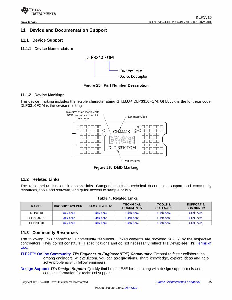
11.1.1 Device Nomenclature
Figure 25. Part Number Description
11.1.2 Device MarkingsThe device marking includes the legible character string GHJJJJK DLP3310FQM. GHJJJJK is the lot trace code.DLP3310FQM is the device marking.
Figure 26. DMD Marking
11.2 Related LinksThe table below lists quick access links. Categories include technical documents, support and communityresources, tools and software, and quick access to sample or buy.
Table 4. Related Links
PARTS PRODUCT FOLDER SAMPLE & BUY TECHNICALDOCUMENTS
TOOLS &SOFTWARE
SUPPORT &COMMUNITY
DLP3310 Click here Click here Click here Click here Click hereDLPC3437 Click here Click here Click here Click here Click hereDLPA3000 Click here Click here Click here Click here Click here
11.3 Community ResourcesThe following links connect to TI community resources. Linked contents are provided "AS IS" by the respectivecontributors. They do not constitute TI specifications and do not necessarily reflect TI's views; see TI's Terms ofUse.
TI E2E™ Online Community TI's Engineer-to-Engineer (E2E) Community. Created to foster collaborationamong engineers. At e2e.ti.com, you can ask questions, share knowledge, explore ideas and helpsolve problems with fellow engineers.
Design Support TI's Design Support Quickly find helpful E2E forums along with design support tools andcontact information for technical support.

36
DLP3310DLPS077B –JUNE 2016–REVISED JANUARY 2018 www.ti.com
Product Folder Links: DLP3310
Submit Documentation Feedback Copyright © 2016–2018, Texas Instruments Incorporated
11.4 TrademarksIntelliBright, E2E are trademarks of Texas Instruments.All other trademarks are the property of their respective owners.
11.5 Electrostatic Discharge CautionThese devices have limited built-in ESD protection. The leads should be shorted together or the device placed in conductive foamduring storage or handling to prevent electrostatic damage to the MOS gates.
11.6 GlossarySLYZ022 — TI Glossary.
This glossary lists and explains terms, acronyms, and definitions.
12 Mechanical, Packaging, and Orderable InformationThe following pages include mechanical, packaging, and orderable information. This information is the mostcurrent data available for the designated devices. This data is subject to change without notice and revision ofthis document. For browser-based versions of this data sheet, refer to the left-hand navigation.
PACKAGE OPTION ADDENDUM
www.ti.com 22-Jun-2018
Addendum-Page 1
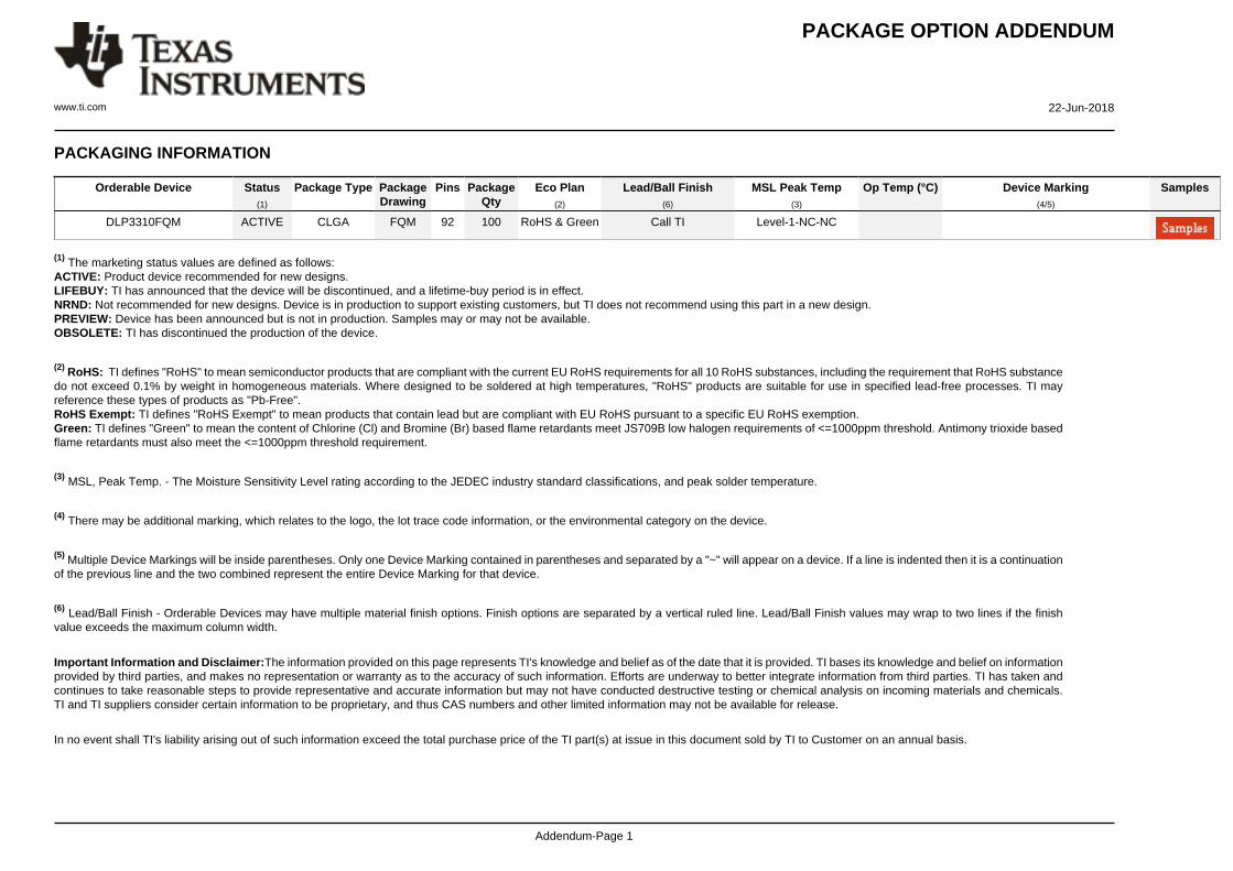
PACKAGING INFORMATION
Orderable Device Status(1)
Package Type PackageDrawing
Pins PackageQty
Eco Plan(2)
Lead/Ball Finish(6)
MSL Peak Temp(3)
Op Temp (°C) Device Marking(4/5)
Samples
DLP3310FQM ACTIVE CLGA FQM 92 100 RoHS & Green Call TI Level-1-NC-NC
(1) The marketing status values are defined as follows:ACTIVE: Product device recommended for new designs.LIFEBUY: TI has announced that the device will be discontinued, and a lifetime-buy period is in effect.NRND: Not recommended for new designs. Device is in production to support existing customers, but TI does not recommend using this part in a new design.PREVIEW: Device has been announced but is not in production. Samples may or may not be available.OBSOLETE: TI has discontinued the production of the device.
(2) RoHS: TI defines "RoHS" to mean semiconductor products that are compliant with the current EU RoHS requirements for all 10 RoHS substances, including the requirement that RoHS substancedo not exceed 0.1% by weight in homogeneous materials. Where designed to be soldered at high temperatures, "RoHS" products are suitable for use in specified lead-free processes. TI mayreference these types of products as "Pb-Free".RoHS Exempt: TI defines "RoHS Exempt" to mean products that contain lead but are compliant with EU RoHS pursuant to a specific EU RoHS exemption.Green: TI defines "Green" to mean the content of Chlorine (Cl) and Bromine (Br) based flame retardants meet JS709B low halogen requirements of <=1000ppm threshold. Antimony trioxide basedflame retardants must also meet the <=1000ppm threshold requirement.
(3) MSL, Peak Temp. - The Moisture Sensitivity Level rating according to the JEDEC industry standard classifications, and peak solder temperature.
(4) There may be additional marking, which relates to the logo, the lot trace code information, or the environmental category on the device.
(5) Multiple Device Markings will be inside parentheses. Only one Device Marking contained in parentheses and separated by a "~" will appear on a device. If a line is indented then it is a continuationof the previous line and the two combined represent the entire Device Marking for that device.
(6) Lead/Ball Finish - Orderable Devices may have multiple material finish options. Finish options are separated by a vertical ruled line. Lead/Ball Finish values may wrap to two lines if the finishvalue exceeds the maximum column width.
Important Information and Disclaimer:The information provided on this page represents TI's knowledge and belief as of the date that it is provided. TI bases its knowledge and belief on informationprovided by third parties, and makes no representation or warranty as to the accuracy of such information. Efforts are underway to better integrate information from third parties. TI has taken andcontinues to take reasonable steps to provide representative and accurate information but may not have conducted destructive testing or chemical analysis on incoming materials and chemicals.TI and TI suppliers consider certain information to be proprietary, and thus CAS numbers and other limited information may not be available for release.
In no event shall TI's liability arising out of such information exceed the total purchase price of the TI part(s) at issue in this document sold by TI to Customer on an annual basis.

SECTION A-A(ROTATED 90°)
SCALE 20 : 1
2 1345678
D
C
B
A
DWG NO. SH8 7 6 5 4 3 1
D
C
B
A
INV11-2006a
2512400 1
TITLE
SIZE DWG NO REV
SCALE SHEET OF
DATE
ENGINEER
QA/CE
CM
APPROVED
DRAWN
INSTRUMENTSDallas Texas
APPLICATIONNEXT ASSY USED ON
THIRD ANGLEPROJECTION
TEXASUNLESS OTHERWISE SPECIFIEDDIMENSIONS ARE IN MILLIMETERSTOLERANCES: ANGLES 1
2 PLACE DECIMALS 0.25
1 PLACE DECIMALS 0.50DIMENSIONAL LIMITS APPLY BEFORE PROCESSESINTERPRET DIMENSIONS IN ACCORDANCE WITH ASME Y14.5M-1994REMOVE ALL BURRS AND SHARP EDGESPARENTHETICAL INFORMATION FOR REFERENCE ONLY
ICD, MECHANICAL, DMD,.33 1080p SERIES 315
(FQM PACKAGE)
25124001 3
CD
3/8/2016
20:1
P. KONRAD
S. SUSI
E. CARPENTER
3/8/2016
3/10/2016
3/10/2016
3/8/2016
0314DA
B. HASKETT
NOTES UNLESS OTHERWISE SPECIFIED:REVISIONSCOPYRIGHT 2016 TEXAS INSTRUMENTS
UN-PUBLISHED, ALL RIGHTS RESERVED.C
B. HASKETT
M. DORAK 3/8/2016
A
A
H H
REV DESCRIPTION DATE BYA ECO 2156795: INITIAL RELEASE 3/8/2016 BMH
B ECO 2157307: UPDATE SUBSTRATE THICKNESS TOLERANCE & SYMBOLIZATION PAD SIZE/SHAPE 4/1/2016 BMH
C ECO 2159285: CORRECT SUBSTRATE BACK SIDE MARKING IN VIEW H-H (SH. 3) FROM "465" TO "888" 7/7/2016 BMH
0.780.063
1.4030.0771.10.05
D
(2.183)
A 3 SURFACES INDICATEDIN VIEW B (SHEET 2)
DIE PARALLELISM TOLERANCE APPLIES TO DMD ACTIVE ARRAY ONLY.
ROTATION ANGLE OF DMD ACTIVE ARRAY IS A REFINEMENT OF THE LOCATIONTOLERANCE AND HAS A MAXIMUM ALLOWED VALUE OF 0.6 DEGREES.
BOUNDARY MIRRORS SURROUNDING THE DMD ACTIVE ARRAY.
NOTCH DIMENSIONS ARE DEFINED BY UPPERMOST LAYERS OF CERAMIC,AS SHOWN IN SECTION A-A.
ENCAPSULANT TO BE CONTAINED WITHIN DIMENSIONS SHOWN IN VIEW C(SHEET 2). NO ENCAPSULANT IS ALLOWED ON TOP OF THE WINDOW.
ENCAPSULANT NOT TO EXCEED THE HEIGHT OF THE WINDOW.
DATUM B IS DEFINED BY A DIA. 2.5 PIN, WITH A FLAT ON THE SIDE FACING TOWARD THE CENTER OF THE ACTIVE ARRAY, AS SHOWN IN VIEW B (SHEET 2).
WHILE ONLY THE THREE DATUM A TARGET AREAS A1, A2, AND A3 ARE USEDFOR MEASUREMENT, ALL 4 CORNERS SHOULD BE CONTACTED, INCLUDING E1,TO SUPPORT MECHANICAL LOADS.
1
4
3
2
7
6
5
8
(ILLUMINATIONDIRECTION)
ACTIVE ARRAY
0.038 A 0.02D
(SHEET 3)(SHEET 3)
4
4 4
4
4
4
4
4
5
8
1
4
4
7
4
8
6
4
(OFF-STATEDIRECTION)
2.5
B
90°1°
3.6 - 0.10.2+
7.2 - 0.10.3+
2.50.075
2.35 - 0.10.2+
1.1760.05
1.25
C
0.4R 0.14X
0.8 - 0.10.2+17.450.08
19.25 - 0.10.3+
(R0.2)4X
1.60.16(2.5)
(1.6)
0 MIN TYP
0.4 MIN TYP
FRONT SIDE INDEX MARK
2X ENCAPSULANT
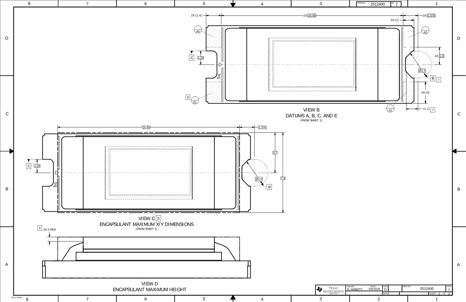
VIEW BDATUMS A, B, C, AND E
(FROM SHEET 1)
VIEW CENCAPSULANT MAXIMUM X/Y DIMENSIONS
(FROM SHEET 1)
VIEW DENCAPSULANT MAXIMUM HEIGHT
2 1345678
D
C
B
A
DWG NO. SH8 7 6 5 4 3 1
D
C
B
A
INV11-2006a
2512400 2
SIZE DWG NO REV
SCALE SHEET OF
DATE
INSTRUMENTSDallas Texas
TEXASDRAWN
25124002 3
CDB. HASKETT 3/8/2016
(1.4)2X 16.852X (1)2X
(2)4X
A3 A2
A1
E1
8
7
7.4
16.85
6
5
2.5
1.251.64X C
B
(1.1)
1.3762X
7
2.5
1.25C
B
3.7
1.376
2X 0 MIN
VIEW EWINDOW AND ACTIVE ARRAY
(FROM SHEET 1)
VIEW H-HBACK SIDE METALLIZATION
(FROM SHEET 1)
DETAIL FAPERTURE LEFT EDGE
SCALE 60 : 1
DETAIL GAPERTURE RIGHT EDGE
SCALE 60 : 1
2 1345678
D
C
B
A
DWG NO. SH8 7 6 5 4 3 1
D
C
B
A
INV11-2006a
2512400 3
SIZE DWG NO REV
SCALE SHEET OF
DATE
INSTRUMENTSDallas Texas
TEXASDRAWN
25124003 3
CDB. HASKETT 3/8/2016
F G
(7.3872)ACTIVE ARRAY
(4.1472)ACTIVE ARRAY
1.2110.05
5.4790.05
(6.69)WINDOW
0.3120.0635
4.5920.0635
(4.904)APERTURE
9.6550.05
3
2
0.2 A B C 0.1 A
(ILLUMINATIONDIRECTION)
(1) 2 3 4 5 6 7 (8)
(0.108)4X
7.6140.06350.4480.0635
(8.062)APERTURE
2.4910.05
(0.15) TYP.
(42°)TYP.
(0.068) TYP. (0.068) TYP.
(0.075) TYP.
(42°)TYP.
A B C D E F G H
2.5
B
1.25C
5.980.075
2.1340.075
(42°)TYP.
16.332822 X 0.7424 =
2.5
B
1.364
1.25C
5.1968= 7 X 0.7424
2.5984
92X SQUARE LGA PADS0.52±0.05 X 0.52±0.05
7X CIRCULAR TEST PADS(Ø0.52)
SYMBOLIZATION PAD
(17) (18) 19 20 21 22 23 24
(12.146) WINDOW
(OFF-STATEDIRECTION)
(7)
(4.64)

IMPORTANT NOTICE
Texas Instruments Incorporated (TI) reserves the right to make corrections, enhancements, improvements and other changes to itssemiconductor products and services per JESD46, latest issue, and to discontinue any product or service per JESD48, latest issue. Buyersshould obtain the latest relevant information before placing orders and should verify that such information is current and complete.TI’s published terms of sale for semiconductor products (http://www.ti.com/sc/docs/stdterms.htm) apply to the sale of packaged integratedcircuit products that TI has qualified and released to market. Additional terms may apply to the use or sale of other types of TI products andservices.Reproduction of significant portions of TI information in TI data sheets is permissible only if reproduction is without alteration and isaccompanied by all associated warranties, conditions, limitations, and notices. TI is not responsible or liable for such reproduceddocumentation. Information of third parties may be subject to additional restrictions. Resale of TI products or services with statementsdifferent from or beyond the parameters stated by TI for that product or service voids all express and any implied warranties for theassociated TI product or service and is an unfair and deceptive business practice. TI is not responsible or liable for any such statements.Buyers and others who are developing systems that incorporate TI products (collectively, “Designers”) understand and agree that Designersremain responsible for using their independent analysis, evaluation and judgment in designing their applications and that Designers havefull and exclusive responsibility to assure the safety of Designers' applications and compliance of their applications (and of all TI productsused in or for Designers’ applications) with all applicable regulations, laws and other applicable requirements. Designer represents that, withrespect to their applications, Designer has all the necessary expertise to create and implement safeguards that (1) anticipate dangerousconsequences of failures, (2) monitor failures and their consequences, and (3) lessen the likelihood of failures that might cause harm andtake appropriate actions. Designer agrees that prior to using or distributing any applications that include TI products, Designer willthoroughly test such applications and the functionality of such TI products as used in such applications.TI’s provision of technical, application or other design advice, quality characterization, reliability data or other services or information,including, but not limited to, reference designs and materials relating to evaluation modules, (collectively, “TI Resources”) are intended toassist designers who are developing applications that incorporate TI products; by downloading, accessing or using TI Resources in anyway, Designer (individually or, if Designer is acting on behalf of a company, Designer’s company) agrees to use any particular TI Resourcesolely for this purpose and subject to the terms of this Notice.TI’s provision of TI Resources does not expand or otherwise alter TI’s applicable published warranties or warranty disclaimers for TIproducts, and no additional obligations or liabilities arise from TI providing such TI Resources. TI reserves the right to make corrections,enhancements, improvements and other changes to its TI Resources. TI has not conducted any testing other than that specificallydescribed in the published documentation for a particular TI Resource.Designer is authorized to use, copy and modify any individual TI Resource only in connection with the development of applications thatinclude the TI product(s) identified in such TI Resource. NO OTHER LICENSE, EXPRESS OR IMPLIED, BY ESTOPPEL OR OTHERWISETO ANY OTHER TI INTELLECTUAL PROPERTY RIGHT, AND NO LICENSE TO ANY TECHNOLOGY OR INTELLECTUAL PROPERTYRIGHT OF TI OR ANY THIRD PARTY IS GRANTED HEREIN, including but not limited to any patent right, copyright, mask work right, orother intellectual property right relating to any combination, machine, or process in which TI products or services are used. Informationregarding or referencing third-party products or services does not constitute a license to use such products or services, or a warranty orendorsement thereof. Use of TI Resources may require a license from a third party under the patents or other intellectual property of thethird party, or a license from TI under the patents or other intellectual property of TI.TI RESOURCES ARE PROVIDED “AS IS” AND WITH ALL FAULTS. TI DISCLAIMS ALL OTHER WARRANTIES ORREPRESENTATIONS, EXPRESS OR IMPLIED, REGARDING RESOURCES OR USE THEREOF, INCLUDING BUT NOT LIMITED TOACCURACY OR COMPLETENESS, TITLE, ANY EPIDEMIC FAILURE WARRANTY AND ANY IMPLIED WARRANTIES OFMERCHANTABILITY, FITNESS FOR A PARTICULAR PURPOSE, AND NON-INFRINGEMENT OF ANY THIRD PARTY INTELLECTUALPROPERTY RIGHTS. TI SHALL NOT BE LIABLE FOR AND SHALL NOT DEFEND OR INDEMNIFY DESIGNER AGAINST ANY CLAIM,INCLUDING BUT NOT LIMITED TO ANY INFRINGEMENT CLAIM THAT RELATES TO OR IS BASED ON ANY COMBINATION OFPRODUCTS EVEN IF DESCRIBED IN TI RESOURCES OR OTHERWISE. IN NO EVENT SHALL TI BE LIABLE FOR ANY ACTUAL,DIRECT, SPECIAL, COLLATERAL, INDIRECT, PUNITIVE, INCIDENTAL, CONSEQUENTIAL OR EXEMPLARY DAMAGES INCONNECTION WITH OR ARISING OUT OF TI RESOURCES OR USE THEREOF, AND REGARDLESS OF WHETHER TI HAS BEENADVISED OF THE POSSIBILITY OF SUCH DAMAGES.Unless TI has explicitly designated an individual product as meeting the requirements of a particular industry standard (e.g., ISO/TS 16949and ISO 26262), TI is not responsible for any failure to meet such industry standard requirements.Where TI specifically promotes products as facilitating functional safety or as compliant with industry functional safety standards, suchproducts are intended to help enable customers to design and create their own applications that meet applicable functional safety standardsand requirements. Using products in an application does not by itself establish any safety features in the application. Designers mustensure compliance with safety-related requirements and standards applicable to their applications. Designer may not use any TI products inlife-critical medical equipment unless authorized officers of the parties have executed a special contract specifically governing such use.Life-critical medical equipment is medical equipment where failure of such equipment would cause serious bodily injury or death (e.g., lifesupport, pacemakers, defibrillators, heart pumps, neurostimulators, and implantables). Such equipment includes, without limitation, allmedical devices identified by the U.S. Food and Drug Administration as Class III devices and equivalent classifications outside the U.S.TI may expressly designate certain products as completing a particular qualification (e.g., Q100, Military Grade, or Enhanced Product).Designers agree that it has the necessary expertise to select the product with the appropriate qualification designation for their applicationsand that proper product selection is at Designers’ own risk. Designers are solely responsible for compliance with all legal and regulatoryrequirements in connection with such selection.Designer will fully indemnify TI and its representatives against any damages, costs, losses, and/or liabilities arising out of Designer’s non-compliance with the terms and provisions of this Notice.
Mailing Address: Texas Instruments, Post Office Box 655303, Dallas, Texas 75265Copyright © 2018, Texas Instruments Incorporated