Embed Size (px)
Citation preview

Rev. 1.1 (April 2012) 1 © DLP Design, Inc.
DDLLPP--HHSS--FFPPGGAA33LEAD FREE
UUSSBB -- FFPPGGAA MMOODDUULLEE
FEATURES: • Xilinx XC3S1400A-4FTG256C FPGA Utilized on the DLP-HS-FPGA3 • Micron 32M x 8 DDR2 SDRAM Memory • Built-In Configuration Loader; Writes the Bit File Directly to SPI Flash via High-Speed USB 2.0
Interface • 63 User I/O Channels: 21 Differential Pairs and 8 Global Clocks • 66.666 MHz Oscillator • 133 MHz DDR2 Interface Reference Design Provided • USB Port Powered or 5V External Power Barrel Jack • USB 1.1 and 2.0 Compatible Interface • Small Footprint: 3.0 x 1.2-Inch PCB and Standard 50-Pin, 0.9-Inch DIP Interface

Rev. 1.1 (April 2012) 2 © DLP Design, Inc.
APPLICATIONS: • Rapid Prototyping • Educational Tool • Industrial/Process Control • Data Acquisition/Processing • Embedded Processor 1.0 INTRODUCTION The DLP-HS-FPGA3 module is a low-cost, compact prototyping tool that can be used for rapid proof of concept or within educational environments. The module is based on the Xilinx Spartan™ 3A and Future Technology Devices International’s FT2232H Dual-Channel High-Speed USB IC. The DLP-HS-FPGA3 provides both the beginner as well as the experienced engineer with a rapid path to developing FPGA-based designs. When combined with the free ISE™ WebPACK™ tools from Xilinx, this module is more than sufficient for creating anything from basic logical functions to a highly complex system controller. As a bonus feature, one channel of the dual-channel USB interface is used to load user bit files directly to the SPI Flash—no external programmer is required. This represents a savings of as much as $200 in that no additional programming cable is required for configuring the FPGA. All that is needed to load bit files to the DLP-HS-FPGA3 is a Windows software utility (free with purchase), a Windows PC and a USB cable. The module can also be programmed from within the Xilinx ISE tool environment using a Xilinx programming cable (purchased separately). The DLP-HS-FPGA3 is fully compatible with the free ISE™ WebPACK™ tools from Xilinx. ISE™ WebPACK™ offers the ideal development environment for FPGA designs with HDL synthesis and simulation, implementation, device fitting and JTAG programming. The DLP-HS-FPGA3 has on-board voltage regulators that generate all required power supply voltages from a single, 5-volt source. Power for the module can be taken from either the host USB port or from a user-supplied, external 5-volt power supply via an onboard standard barrel connector.
Connection to user electronics is made via a 50-pin, 0.9-inch wide, industry-standard 0.025-square inch post DIP header on the bottom of the board and a 26-pin, 0.05-inch wide top-side 2x13 header. The bottom-side 50-pin header provides access to 41 of the FPGA user input/output pins. The top-side header provides access to 22 of the FPGA user input/output pins. The bottom-side header mates with a user-supplied, standard, 50-pin, 0.9-inch spaced DIP socket. The top-side header mates with a user-supplied, 0.05-inch spaced, 2x13 connector such as the FFSD-13-D-xx.xx-01 (xx.xx = cable length) ribbon cable assembly from Samtec.

Rev. 1.1 (April 2012) 3 © DLP Design, Inc.
DIP Socket
Ribbon Cable
Other on-board features include a 32M x 8 DDR2 SDRAM memory IC for user projects and both JTAG and SPI Flash interface ports for connection to Xilinx programming tools. 2.0 REFERENCE DESIGN A 10,000-line reference design is available for the Spartan™ 3A FPGA on the DLP-HS-FPGA3 to those who purchase the module. The design was written in VHDL and built using the free Xilinx ISE™ WebPACK™ tools. The reference design consists of the following blocks:
It contains a USB Interface Block, a User I/0 Block, a DDR2 SDRAM interface, a Heartbeat Pulse Generator and a Clock Generator. The SPI Flash is used to store the design’s FPGA configuration file. The USB interface captures, interprets and returns command and data information sent from the host PC through the FTDI USB interface to the FPGA. Commands include Ping, Return Status, Loopback Data, Set a User I/O Pin High or Low, Read a User I/O Pin, Initialize the DDR2 SDRAM Memory and Read (from) or Write (to) the DDR2 SDRAM Memory. (Section 11 explains these in detail.)

Rev. 1.1 (April 2012) 4 © DLP Design, Inc.
The User I/O Block controls access to the 63 user I/O pins accessible through the top- and bottom- side headers. Every one of these pins can be either an input or an output. The User I/O Block can configure these pins as inputs and read their state, or as outputs and drive them high or low. (As a side note, 48 of these user I/O pins can be configured as 24 differential pairs, 8 can be configured as global clock inputs and 6 can be configured as regional clock inputs.) The DDR2 SDRAM interface block manages the memory’s initialization, the refresh cycle and the read and write access. Read and write access is available in 4-byte bursts. The traces between the DDR2 SDRAM and FPGA are matched within 10 mils to accommodate reliable data transfer at 266 Mbit/s (clocked at 133MHz). The interface creates and aligns the Data Strobes (DQS) based on an external feedback trace that matches two times the trace length between the FPGA and the DDR2 SDRAM. The Initialization, Read and Write commands are initiated by the USB interface block and executed by the DDR2 SDRAM interface block. The Heartbeat Pulse Generator takes the internal system clock and divides it down so that the onboard Heartbeat LED will be turned on and off for a duration of approximately one-half second. The Clock Generator Block receives the 66.666-MHz clock and produces both the 133-MHz clocks required to run the DDR2 SDRAM memory device and the 100-MHz clock for the remaining internal logic in the FPGA. It also handles reset and lock synchronization between internal DCM blocks. The design occupies the following FPGA resources on the DLP-HS-FPGA3 module’s XC3S1400A:
More reference designs are planned. Please contact DLP Design with any specific requests.

Rev. 1.1 (April 2012) 5 © DLP Design, Inc.
3.0 FPGA SPECIFICATIONS
The FPGA device used on the DLP-HS-FPGA3 is the Xilinx Spartan™ 3A: • Part Number: XC3S1400A-4FTG256C • System Gates: 1,400,000 • Equivalent Logic Cells: 25,344 • CLB Array:
Rows: 72 Columns: 40 Total CLB’s: 2,816 Total Slices: 11,264 Total Flip Flops: 22,528 Total 4-Input LUT’s: 22,528
• Distributed RAM Bits: 176K • Block RAM Bits: 576K • Dedicated Multipliers: 32 • DCM’s: 8 4.0 ABSOLUTE MAXIMUM RATINGS Stresses above those listed here may cause permanent damage to the DLP-HS-FPGA3: Operating Temperature: 0-70°C Voltage on Digital Inputs with Respect to Ground: -0.5V to +4.1 V Sink/Source Current on Any I/O: 24 mA (using LVTTL as the FPGA I/O standard) 5.0 WARNINGS • Unplug from the host PC and power adapter before connecting to I/O on the DLP-HS-FPGA3.
• Isolate the bottom of the board from all conductive surfaces.
• Observe static precautions to prevent damage to the DLP-HS-FPGA3 module.

Rev. 1.1 (April 2012) 6 © DLP Design, Inc.
6.0 BITLOADAPP SOFTWARE Windows software is provided for use with the DLP-HS-FPGA3 that will load an FPGA configuration (*.bit) file directly to the SPI Flash device via the USB interface. This application (illustrated below) will allow the user to erase the Flash, verify the erasure and then program and verify the Flash:
7.0 JTAG INTERFACE The easiest way to load an FPGA configuration (*.bit) file to the FPGA is to run the BitLoadApp software then select and program a file from the local hard drive directly to the SPI Flash. Once written to the SPI Flash, the configuration will load to the FPGA and execute. Alternatively, a traditional JTAG header location is provided on the DLP-HS-FPGA3 giving the user access to the specific pins required by the development tools. (Refer to the schematic contained within this datasheet for details.) 8.0 EEPROM SETUP / MPROG The DLP-HS-FPGA3 has a dual-channel USB interface to the host PC. Channel B is used exclusively to load an FPGA configuration (*.bit) file to the SPI Flash. This configuration data is automatically transferred to the FPGA when power is applied to the module or when the PROG pin is driven low and then released by the application software. Channel A is used for communication between the FPGA and the host PC at run time. A 93LC56B EEPROM connected to the USB interface IC is used to store the setup for the two channels. The parameters stored in the EEPROM include the Vendor ID (VID), Product ID (PID), Serial Number, Description String, driver selection (VCP or D2XX) and port type (UART serial or FIFO parallel). As mentioned above, Channel B is used exclusively for loading the FPGA’s configuration to the SPI Flash, and Channel A is used for communication between the host PC and the DLP-HS-FPGA3. As such, the D2XX drivers and 245 FIFO mode must be selected in the EEPROM for Channel B. Channel A must use the 245 FIFO mode, but it can use either the VCP or D2XX drivers. The VCP drivers make the DLP-HS-FPGA3 appear as an RS232 port to the host application. The D2XX drivers provide faster throughput but require working with a *.lib or *.dll library in the host application. The operational modes and other EEPROM selections are written to the EEPROM using the MPROG utility. This utility and its manual are available for download from the bottom of the page at www.dlpdesign.com.

Rev. 1.1 (April 2012) 7 © DLP Design, Inc.
9.0 TEST BIT FILE A test file is provided as a download from the DLP Design website that provides rudimentary access to the I/O features of the DLP-HS-FPGA3. The following features are provided: • Ping
• Read the High/Low State of the Input-Only Pins
• Drive I/O Pins High/Low or Read their High/Low State
• Simple Loopback on Channel A
• 4-Byte Read/Write Access of the Row, Column, and Bank Address in the DDR2 SDRAM This bit file is available from the DLP-HS-FPGA3 download page. The command structure that supports these features is explained in Section 11. 10.0 USB DRIVERS USB drivers for the following operating systems are available for download from the DLP Design website at www.dlpdesign.com:
OPERATING SYSTEM SUPPORT Windows 7 32-bit Windows 7 64-bit
Windows Vista, Vista x64 Mac OSX Windows XP, XP x64 Mac OS9
Windows Server 2008, x64 Mac OS8 Windows Server 2003, x64 Linux
Windows 2000 Windows CE 4.2 – 6.0 Notes: 1. The bit file load utility only runs on the Windows platforms. 2. The bit file load utility requires the use of USB channel B, and channel B is dedicated to this
function. 3. If you are utilizing the dual-mode drivers from FTDI (CDM2.x.x) and you want to use the Virtual COM Port (VCP) drivers, then it may be necessary to disable the D2XX drivers first via Device Manager. To do so, right click on the entry under USB Controllers that appears when the
DLP-HS-FPGA3 is connected, select Properties, select the Advanced tab, check the option for “Load VCP” and click OK. Then unplug and replug the DLP-HS-FPGA3, and a COM port should appear in Device Manager under Ports (COM & LPT).

Rev. 1.1 (April 2012) 8 © DLP Design, Inc.
11.0 USING THE DLP-HS-FPGA3 Select a power source via Header Pins 23 and 24, and connect the DLP-HS-FPGA3 to the PC to initiate loading of the USB drivers. The easiest way to do this is to connect Pins 23 and 24 to each other. This will result in operational power being taken from the host PC. Once the drivers are loaded, the DLP-HS-FPGA3 is ready for use.
Simply connect the DLP-HS-FPGA3 to the PC to initiate the loading of USB drivers.
You can either utilize the Test Application available from http://www.dlpdesign.com/test.shtml with the DLP-HS-FPGA3 (as described in Section 12), or you can write your own program in your language of choice. If you are using the VCP drivers, begin by opening the COM port, and send multi-byte commands as shown in Table 1 below. There is no need to set the baud rate because the DLP-HS-FPGA3 uses a parallel interface between the USB IC and the FPGA. (The Ping Command can be used to locate the correct COM port used for communicating with the DLP-HS-FPGA3, or you can look in Device Manager to see which port was assigned by Windows.) If you are using the D2XX drivers as with the Test Application, no COM port selection is necessary.
TABLE 1

Rev. 1.1 (April 2012) 9 © DLP Design, Inc.
Command Packets Command
Packet Description
Byte
Hex Value
Return/Comments
Ping Issues Ping 0 0x00 Ping Command - 0x56 will be returned indicating that the DLP-HS-FPGA3 is found on the selected port.
Read Version/ Status
Accesses the internal version/ status registers
0 0x10 Read Version/Status Registers Command 1 0xnn Register Address: 0xnn =
0x00 = Board ID (0x30 = Production PCB) 0x01 = FPGA Type ID : 0x6A = XC3S1400A 0x02 = Design Version ID 1 (Design Month) 0x03 = Design Version ID 2 (Design Day) 0x04 = Design Version ID 3 (Design Year) 0x05 = Design Version ID 4 (Design Version) 0x06 = DDR2 Status: 0x00 = Not Initialized 0x01 = Initialized
Loopback Returns the data byte received
0 0x20 Loopback Command 1 0xnn The byte sent to the DLP-HS-FPGA3 (0xnn) will be
returned back. Loopback
Compliment Returns the compliment of data byte received
0 0x21 Loopback Compliment Command 1 0xnn The byte sent to the DLP-HS-FPGA3 (0xnn) will be
complimented and returned back.
Read Pin Reads the state of one of the user I/O pins
0 0x30 Read Pin Command 1 0x00
– 0x3E
The user I/O pin numbers are described in Table 2. User I/O pin 0xnn is read and returns: 0x00 = User I/O pin 0xnn is low 0x01 = User I/O pin 0xnn is high
Clear Pin Forces the selected user I/O pin low
0 0x40 Clear Pin Command 1 0x00
– 0x3E
The user I/O pin numbers are described in Table 2. User I/O pin 0xnn is cleared. The specified user I/O number is returned.
Set Pin Forces the selected user I/O pin high
0 0x41 Set Pin Command 1 0x00
– 0x3E
The user I/O pin numbers are described in Table 2. User I/O pin 0xnn is set. The specified user I/O number is returned.
Initialize Memory
Initializes DDR2 SDRAM
0 0x70 The Initialize Memory Command configures the DDR2 SDRAM for access by the FPGA. The memory cannot be accessed without being initialized.
IMPORTANT NOTE ON DDR2 SDRAM DATA ACCESS: Writes and reads made to and from the DDR2 SDRAM using the reference design on the DLP-HS-FPGA3 module are always performed 4 bytes at a time due to the fact that the device is configured for a burst length of four. What this means is that Column Address Bits 0 and 1 only change the order of the read or write bytes; they still refer to the same 4 bytes. Therefore, to increment the DDR2 SDRAM address for consecutive memory locations, the column address must be incremented by 4. Incrementing the column address by anything less than 4 simply changes the order in which the 4 bytes specified by Column Address 9:3 are written to the memory or returned to the user.
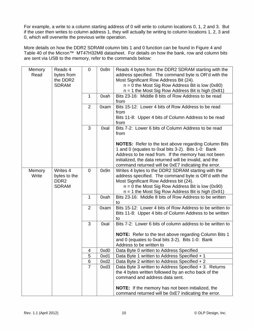
Rev. 1.1 (April 2012) 10 © DLP Design, Inc.
For example, a write to a column starting address of 0 will write to column locations 0, 1, 2 and 3. But if the user then writes to column address 1, they will actually be writing to column locations 1, 2, 3 and 0, which will overwrite the previous write operation. More details on how the DDR2 SDRAM column bits 1 and 0 function can be found in Figure 4 and Table 40 of the Micron™ MT47H32M8 datasheet. For details on how the bank, row and column bits are sent via USB to the memory, refer to the commands below:
Memory Read
Reads 4 bytes from the DDR2 SDRAM
0 0x8n Reads 4 bytes from the DDR2 SDRAM starting with the address specified. The command byte is OR’d with the Most Significant Row Address Bit (24). n = 0 the Most Sig Row Address Bit is low (0x80) n = 1 the Most Sig Row Address Bit is high (0x81)
1 0xah Bits 23-16: Middle 8 bits of Row Address to be read from
2 0xam Bits 15-12: Lower 4 bits of Row Address to be read from Bits 11-8: Upper 4 bits of Column Address to be read from
3 0xal Bits 7-2: Lower 6 bits of Column Address to be read from NOTES: Refer to the text above regarding Column Bits 1 and 0 (equates to 0xal bits 3-2). Bits 1-0: Bank Address to be read from. If the memory has not been initialized, the data returned will be invalid, and the command returned will be 0xE7 indicating the error.
Memory Write
Writes 4 bytes to the DDR2 SDRAM
0 0x9n Writes 4 bytes to the DDR2 SDRAM starting with the address specified. The command byte is OR’d with the Most Significant Row Address bit (24). n = 0 the Most Sig Row Address Bit is low (0x90) n = 1 the Most Sig Row Address Bit is high (0x91)
1 0xah Bits 23-16: Middle 8 bits of Row Address to be written to
2 0xam Bits 15-12: Lower 4 bits of Row Address to be written to Bits 11-8: Upper 4 bits of Column Address to be written to
3 0xal Bits 7-2: Lower 6 bits of column address to be written to NOTE: Refer to the text above regarding Column Bits 1 and 0 (equates to 0xal bits 3-2). Bits 1-0: Bank Address to be written to
4 0xd0 Data Byte 0 written to Address Specified 5 0xd1 Data Byte 1 written to Address Specified + 1 6 0xd2 Data Byte 2 written to Address Specified + 2 7 0xd3 Data Byte 3 written to Address Specified + 3. Returns
the 4 bytes written followed by an echo back of the command and address data sent. NOTE: If the memory has not been initialized, the command returned will be 0xE7 indicating the error.
Rev. 1.1 (April 2012) 11 © DLP Design, Inc.
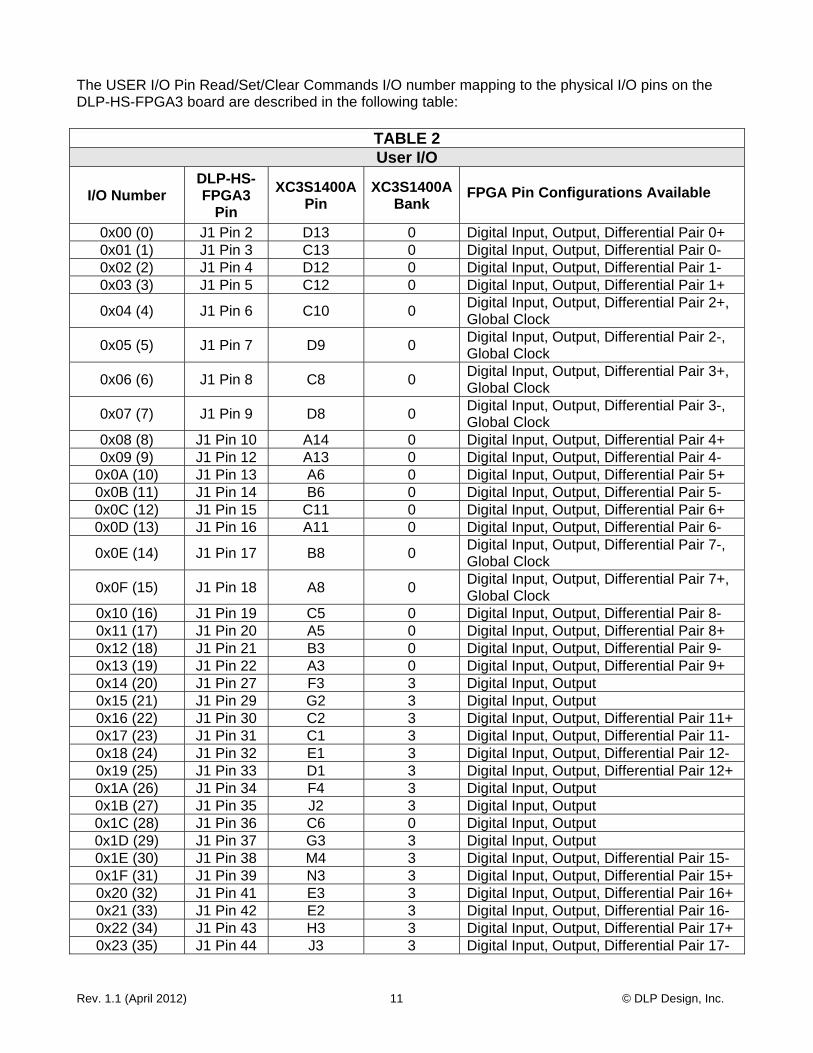
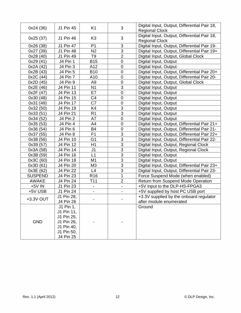
The USER I/O Pin Read/Set/Clear Commands I/O number mapping to the physical I/O pins on the DLP-HS-FPGA3 board are described in the following table:
TABLE 2 User I/O
I/O Number DLP-HS-FPGA3
Pin XC3S1400A
Pin XC3S1400A
Bank
FPGA Pin Configurations Available
0x00 (0) J1 Pin 2 D13 0 Digital Input, Output, Differential Pair 0+ 0x01 (1) J1 Pin 3 C13 0 Digital Input, Output, Differential Pair 0- 0x02 (2) J1 Pin 4 D12 0 Digital Input, Output, Differential Pair 1-0x03 (3) J1 Pin 5 C12 0 Digital Input, Output, Differential Pair 1+
0x04 (4) J1 Pin 6 C10 0 Digital Input, Output, Differential Pair 2+, Global Clock
0x05 (5) J1 Pin 7 D9 0 Digital Input, Output, Differential Pair 2-, Global Clock
0x06 (6) J1 Pin 8 C8 0 Digital Input, Output, Differential Pair 3+, Global Clock
0x07 (7) J1 Pin 9 D8 0 Digital Input, Output, Differential Pair 3-, Global Clock
0x08 (8) J1 Pin 10 A14 0 Digital Input, Output, Differential Pair 4+0x09 (9) J1 Pin 12 A13 0 Digital Input, Output, Differential Pair 4-
0x0A (10) J1 Pin 13 A6 0 Digital Input, Output, Differential Pair 5+0x0B (11) J1 Pin 14 B6 0 Digital Input, Output, Differential Pair 5-0x0C (12) J1 Pin 15 C11 0 Digital Input, Output, Differential Pair 6+0x0D (13) J1 Pin 16 A11 0 Digital Input, Output, Differential Pair 6-
0x0E (14) J1 Pin 17 B8 0 Digital Input, Output, Differential Pair 7-, Global Clock
0x0F (15) J1 Pin 18 A8 0 Digital Input, Output, Differential Pair 7+, Global Clock
0x10 (16) J1 Pin 19 C5 0 Digital Input, Output, Differential Pair 8-0x11 (17) J1 Pin 20 A5 0 Digital Input, Output, Differential Pair 8+0x12 (18) J1 Pin 21 B3 0 Digital Input, Output, Differential Pair 9-0x13 (19) J1 Pin 22 A3 0 Digital Input, Output, Differential Pair 9+0x14 (20) J1 Pin 27 F3 3 Digital Input, Output 0x15 (21) J1 Pin 29 G2 3 Digital Input, Output 0x16 (22) J1 Pin 30 C2 3 Digital Input, Output, Differential Pair 11+0x17 (23) J1 Pin 31 C1 3 Digital Input, Output, Differential Pair 11-0x18 (24) J1 Pin 32 E1 3 Digital Input, Output, Differential Pair 12-0x19 (25) J1 Pin 33 D1 3 Digital Input, Output, Differential Pair 12+0x1A (26) J1 Pin 34 F4 3 Digital Input, Output 0x1B (27) J1 Pin 35 J2 3 Digital Input, Output 0x1C (28) J1 Pin 36 C6 0 Digital Input, Output 0x1D (29) J1 Pin 37 G3 3 Digital Input, Output 0x1E (30) J1 Pin 38 M4 3 Digital Input, Output, Differential Pair 15-0x1F (31) J1 Pin 39 N3 3 Digital Input, Output, Differential Pair 15+0x20 (32) J1 Pin 41 E3 3 Digital Input, Output, Differential Pair 16+0x21 (33) J1 Pin 42 E2 3 Digital Input, Output, Differential Pair 16-0x22 (34) J1 Pin 43 H3 3 Digital Input, Output, Differential Pair 17+0x23 (35) J1 Pin 44 J3 3 Digital Input, Output, Differential Pair 17-
Rev. 1.1 (April 2012) 12 © DLP Design, Inc.
0x24 (36) J1 Pin 45 K1 3 Digital Input, Output, Differential Pair 18, Regional Clock
0x25 (37) J1 Pin 46 K3 3 Digital Input, Output, Differential Pair 18, Regional Clock
0x26 (38) J1 Pin 47 P1 3 Digital Input, Output, Differential Pair 19-0x27 (39) J1 Pin 48 N2 3 Digital Input, Output, Differential Pair 19+0x28 (40) J1 Pin 49 T9 2 Digital Input, Output, Global Clock0x29 (41) J4 Pin 1 B15 0 Digital Input, Output 0x2A (42) J4 Pin 3 A12 0 Digital Input, Output 0x2B (43) J4 Pin 5 B10 0 Digital Input, Output, Differential Pair 20+0x2C (44) J4 Pin 7 A10 0 Digital Input, Output, Differential Pair 20-0x2D (45) J4 Pin 9 A9 0 Digital Input, Output, Global Clock0x2E (46) J4 Pin 11 N1 3 Digital Input, Output 0x2F (47) J4 Pin 13 E7 0 Digital Input, Output 0x30 (48) J4 Pin 15 C4 0 Digital Input, Output 0x31 (49) J4 Pin 17 C7 0 Digital Input, Output 0x32 (50) J4 Pin 19 K4 3 Digital Input, Output 0x33 (51) J4 Pin 21 R1 3 Digital Input, Output 0x34 (52) J4 Pin 2 A7 0 Digital Input, Output 0x35 (53) J4 Pin 4 A4 0 Digital Input, Output, Differential Pair 21+0x36 (54) J4 Pin 6 B4 0 Digital Input, Output, Differential Pair 21-0x37 (55) J4 Pin 8 F1 3 Digital Input, Output, Differential Pair 22+0x38 (56) J4 Pin 10 G1 3 Digital Input, Output, Differential Pair 22-0x39 (57) J4 Pin 12 H1 3 Digital Input, Output, Regional Clock0x3A (58) J4 Pin 14 J1 3 Digital Input, Output, Regional Clock0x3B (59) J4 Pin 16 L1 3 Digital Input, Output 0x3C (60) J4 Pin 18 M1 3 Digital Input, Output 0x3D (61) J4 Pin 20 M3 3 Digital Input, Output, Differential Pair 23+0x3E (62) J4 Pin 22 L4 3 Digital Input, Output, Differential Pair 23-SUSPEND J4 Pin 23 R16 1 Force Suspend Mode (when enabled)
AWAKE J4 Pin 24 T11 2 Return from Suspend Mode Operation +5V IN J1 Pin 23 - - +5V input to the DLP-HS-FPGA3
+5V USB J1 Pin 24 - - +5V supplied by host PC USB port
+3.3V OUT J1 Pin 28, J4 Pin 26 - - +3.3V supplied by the onboard regulator
after module enumerated
GND
J1 Pin 1, J1 Pin 11, J1 Pin 25, J1 Pin 26, J1 Pin 40, J1 Pin 50, J4 Pin 25
- -
Ground

Rev. 1.1 (April 2012) 13 © DLP Design, Inc.
12.0 USING THE DLP TEST APPLICATION (OPTIONAL) Users can design their own application interface to send USB commands to the DLP-HS-FPGA3 module or utilize the test application tool available from DLP Design. The DLP Test Application is available in a free version for download from the DLP Design website at www.dlpdesign.com/ test.shtml. Using this tool, single- and multi-byte commands can be sent to the DLP-HS-FPGA3 board. Once installed the test application is used as follows:
The commands used to interface to the DLP-HS-FPGA3 are detailed in Section 11 of this datasheet.

Rev. 1.1 (April 2012) 14 © DLP Design, Inc.
13.0 MECHANICAL DIMENSIONS IN INCHES (MM) (PRELIMINARY)

Rev. 1.1 (April 2012) 15 © DLP Design, Inc.
14.0 DISCLAIMER © DLP Design, Inc., 2000-2012 Neither the whole nor any part of the information contained herein nor the product described in this manual may be adapted or reproduced in any material or electronic form without the prior written consent of the copyright holder. This product and its documentation are supplied on an as-is basis, and no warranty as to their suitability for any particular purpose is either made or implied. DLP Design, Inc. will not accept any claim for damages whatsoever arising as a result of the use or failure of this product. Your statutory rights are not affected. This product or any variant of it is not intended for use in any medical appliance, device or system in which the failure of the product might reasonably be expected to result in personal injury. This document provides preliminary information that may be subject to change without notice. 15.0 CONTACT INFORMATION DLP Design, Inc. 1605 Roma Lane Allen, TX 75013 Phone: 469-964-8027 Fax: 415-901-4859 Email Sales: [email protected] Email Support: [email protected] Website URL: http://www.dlpdesign.com

55
44
33
22
11
DD
CC
BB
AA
PRELIMINARY
DL
P-H
S-F
PG
A3
Pa
ge
1
v1.0
1000 mA
DC
:+3.6
to +
6.0
V
13
2
Bottom side FPGA IO (top view)
Top side FPGA IO
For FPGA configuration
via SPI only.
DNS
Downloading
FPGA Code
UPLOAD
DNS
DNS
DNS
DNSPOWER-UP DELAY CAP C78
200uS (No cap) to 300mS (0.1uF)
EE
DA
TA
PW
RE
N#
EE
CS
P1V
8
EE
SK
P5V
0U
SE
R_IO
39_D
P19
US
ER
_IO
36_D
N18_R
C
US
ER
_IO
31_D
P15
US
ER
_IO
2_D
N1
US
ER
_IO
33_D
N16
US
ER
_IO
38_D
N19
US
ER
_IO
40_G
C
US
ER
_IO
3_D
P1
US
ER
_IO
32_D
P16
US
ER
_IO
34_D
P17_R
CU
SE
R_IO
5_D
N2_G
CU
SE
R_IO
35_D
N17_R
C
US
ER
_IO
0_D
P0
US
ER
_IO
18_D
N9
US
ER
_IO
13_D
N6
US
ER
_IO
17_D
P8
US
ER
_IO
24_D
N12
US
ER
_IO
23_D
N11
US
ER
_IO
12_D
P6
US
ER
_IO
20
US
ER
_IO
26
US
ER
_IO
21
US
ER
_IO
25_D
P12
US
ER
_IO
37_D
P18_R
C
US
ER
_IO
22_D
P11
US
ER
_IO
11_D
N5
US
ER
_IO
16_D
N8
US
ER
_IO
19_D
P9
US
ER
_IO
15_D
P7_G
CU
SE
R_IO
14_D
N7_G
CU
SE
R_IO
27
US
ER
_IO
7_D
N3_G
C
US
ER
_IO
29
US
ER
_IO
6_D
P3_G
C
US
ER
_IO
8_D
P4
US
ER
_IO
28
US
ER
_IO
9_D
N4
US
ER
_IO
30_D
N15
US
ER
_IO
4_D
P2_G
C
US
ER
_IO
1_D
N0
VP
LL
VP
HY
VP
LL
VP
HY
PO
RT
VC
C
5V
IN
VC
CS
W
PO
RT
VC
C
5V
INU
SE
R_IO
10_D
P5
US
ER
_IO
41
US
ER
_IO
52
US
ER
_IO
42
US
ER
_IO
43_D
P20
US
ER
_IO
44_D
N20
US
ER
_IO
45_G
CU
SE
R_IO
46
US
ER
_IO
47
US
ER
_IO
48
US
ER
_IO
49
US
ER
_IO
50
US
ER
_IO
51
FP
GA
_S
US
PE
ND
US
ER
_IO
53_D
P21
US
ER
_IO
54_D
N21
US
ER
_IO
55_D
P22
US
ER
_IO
56_D
N22
US
ER
_IO
57_R
CU
SE
R_IO
58_R
CU
SE
R_IO
59
US
ER
_IO
60
US
ER
_IO
61_D
P23
US
ER
_IO
62_D
N23
FP
GA
_A
WA
KE
VC
CS
W
FT
DI_
RD
FT
DI_
SI
FT
DI_
RX
F
FT
DI_
WR
FT
DI_
D6
FT
DI_
D5
FT
DI_
D2
FT
DI_
D4
FT
DI_
D3
FT
DI_
TX
E
FT
DI_
D7
FT
DI_
D0
FT
DI_
D1
SP
I_C
LK
SP
I_M
OS
IS
PI_
DIN
SP
I_C
SO
_B
SP
I_P
RO
G
FP
GA
_A
WA
KE
FP
GA
_S
US
PE
ND
FP
GA
_R
ES
ET
FT
DI_
CLK
OU
T
US
ER
_IO
63
VC
CS
W
US
ER
_IO
64
5V
0
3V
3
3V
3
3V
3
3V
3
3V
3
3V
33V
3
5V
0
3V
3
5V
0
3V
3
R36
0
CN
1C
N-U
SB
1234
5
C8
1.0
uF
/0603
C77
.1uF
CN
2DC
BA
RR
EL J
AC
K
2 3 1
D4
MB
R130T
1G
C2
.1uF
TP
4S
PA
RE
_B
DB
US
31
C1
.01
C47
.1uF
C78
1000pF
R38
0
R24
2.2
K
C18
0.1
uF
JP
3
PR
OG
Dis
able
12
R31
1K
J1
CO
NN
PC
B 2
5x2
8 7 6 12345
10 9
12
11
13
15
14
17
16
18
20
19
25
24
23
22
21
34
33
32
31
30
29
28
27
26
40
39
38
37
36
35
50
49
48
47
46
45
44
43
42
41
8 7 6 1234510
912
11
13
15
14
17
16
18
20
19
25
24
23
22
21
34
33
32
31
30
29
28
27
26
40
39
38
37
36
35
50
49
48
47
46
45
44
43
42
41
Q2
IRLM
L6402
R27
24.9
K
Y1
12M
Hz
FB
2240-1
018-1
12
C5
.1uF
C48
.1uF
R3
10K
R33
27
C39
10uF
/10V
C17
0.1
uF
R28
10K
5%
R4
2.2
K
C3
.1uF
R19
0
U1
FT
1232H
Q
5147
4256
8
62
3120
643712
94
507
10
1511152535
59
58
57
55
54
53
52
48
16
17
18
19
21
22
23
24
26
27
28
29
30
32
33
34
38
39
40
41
43
44
45
46
3 2
146
49
63
61
13
60
36
GNDGND
VCCIOVCCIO
DP
EE
CLK
VCCIOVCCIO
VCOREVCOREVCORE
VPLLVPHY
VR
EG
IN
DM
AGND
GNDGNDGNDGNDGNDGND
BC
BU
S7/P
WR
SA
V#/P
WR
SA
V#/G
PIO
H7
BC
BU
S6/-/-/G
PIO
H6
BC
BU
S5/-/-/G
PIO
H5
BC
BU
S4/R
XLE
D#/S
IWU
B/G
PIO
H4
BC
BU
S3/T
XLE
D#/W
R#/G
PIO
H3
BC
BU
S2/R
DS
TB
#/R
D#/G
PIO
H2
BC
BU
S1/W
RS
TB
#/T
XE
#/G
PIO
H1
BC
BU
S0/T
XD
EN
/RX
F#/G
PIO
H0
AD
BU
S0/T
XD
/D0/T
CK
SK
AD
BU
S1/R
XD
/D1/T
DI D
OA
DB
US
2/R
TS
#/D
2/T
DO
DI
AD
BU
S3/C
TS
#/D
3/T
MS
CS
AD
BU
S4/D
TR
#/D
4/G
PIO
L0
AD
BU
S5/D
SR
#/D
5/G
PIO
L1
AD
BU
S6/D
CD
#/D
6/G
PIO
L2
AD
BU
S7/R
I#/D
7/G
PIO
L3
AC
BU
S0/T
XD
EN
/RX
F#/G
PIO
H0
AC
BU
S1/W
RS
TB
#/T
XE
#/G
PIO
H1
AC
BU
S2/R
DS
TB
#/R
D#/G
PIO
H2
AC
BU
S3/T
XLE
D#/W
R#/G
PIO
H3
AC
BU
S4/R
XLE
D#/S
IWU
A/G
PIO
H4
AC
BU
S5/-/C
LK
OU
T/G
PIO
H5
AC
BU
S6/-/O
E#/G
PIO
H6
AC
BU
S7/-/-/G
PIO
H7
BD
BU
S0/T
XD
/DO
/TC
K S
KB
DB
US
1/R
XD
/D1/T
DI D
OB
DB
US
2/R
TS
#/D
2/T
DO
DI
BD
BU
S3/C
TS
#/D
3/T
MS
CS
BD
BU
S4/D
TR
#/D
4/G
PIO
L0
BD
BU
S5/D
SR
#/D
5/G
PIO
L1
BD
BU
S6/D
CD
#/D
6/G
PIO
L3
BD
BU
S7/R
I#/D
7/G
PIO
L4
OS
CO
OS
CI
RE
SE
T#
RE
F
VR
EG
OU
T
EE
CS
EE
DA
TA
TE
ST
PW
RE
N#
SU
SP
EN
D#
C33
.1uF
C34
10/1
0 T
ant
Q4
MM
BT
3904L
3
1
2
R39
100K
FB
3240-1
018-1
12
J4
CO
NN
HD
R 1
3x2
15
13
11 13579
19
17
23
21
25
22
24
26
246810
12
14
16
18
20
15
13
11
1357919
17
23
21
25
22
24
26 2468
10
12
14
16
18
20
FB
1240-1
018-1
12
R34
0
C4
.1uF
R37
0
D5
RE
D
C9
.1uF
C49
.1uF
R35
0
R6
10K
R32
0
C10
4.7
uF
C11
27pF
U3
93LC
46
1234
8765
CS
SK
DIN
DO
UT
VC
CN
CN
C/O
RG
GN
D
R16
27
TP
5S
PA
RE
_B
DB
US
51
C6
4.7
uF
R17
27
R2
12K
C26
.1uF
R13
150
C85
.1uF
C19
10/1
0 T
ant
R7
10K
C25
4.7
uF
TP
6S
PA
RE
_B
CB
US
11
U2
MC
P1726-3
302E
/MF
81
5
4 23
76
VO
UT
VIN
PW
RG
D
GN
D
VIN
SH
DN
VO
UT
CD
ELA
Y
C46
.1uF
C12
27pF

55
44
33
22
11
DD
CC
BB
AA
PRELIMINARY
Pa
ge
2
DL
P-H
S-F
PG
A3
TDI
SPI
Flash
TMS
TDO
TCK
350mA Maximum
1.5A Maximum
1.2
V R
EG
UL
AT
OR
1.8
V R
EG
UL
AT
OR
2.5 mS ramp up
DD
R II p
ara
llel
term
ina
tion
s
Use Ceramic caps
DNS
DNS
V1
.0
DNS
DNS
DNS
DNSDNS
DNS
DNS
DNS
SP
I_P
RO
G
JT
AG
_D
INJT
AG
_T
MS
JT
AG
_T
CK
JT
AG
_D
OU
T
JT
AG
_T
MS
JT
AG
_T
CK
JT
AG
_D
INJT
AG
_D
OU
TLE
DG
_D
ON
E
SP
I_D
IN
SP
I_C
LK
SP
I_M
OS
I
SP
I_C
SO
_B
VC
CS
W
VR
EF
_0V
9
VT
T_0V
9
DD
R2_A
10
DD
R2_R
FU
_B
A2
VT
T_0V
9
VT
T_0V
9
DD
R2_A
11
DD
R2_A
6D
DR
2_R
FU
_A
15
DD
R2_A
4
DD
R2_B
A1
DD
R2_B
A0
VT
T_0V
9
DD
R2_A
7D
DR
2_A
12
DD
R2_A
3D
DR
2_W
En
DD
R2_R
FU
_A
14
DD
R2_A
9
DD
R2_A
1D
DR
2_A
5
DD
R2_A
2
DD
R2_C
KE
DD
R2_R
FU
_A
13
DD
R2_A
8D
DR
2_O
DT
DD
R2_R
AS
nD
DR
2_C
Sn
DD
R2_C
AS
nD
DR
2_A
0
VT
T_0V
9
VT
T_0V
9
VT
T_0V
9
CLK
IN
VC
CS
W
1V
2
VC
CS
W
VC
CS
W
VC
CS
W
VC
CS
W
VC
CS
W
1V
2
1V
8
VC
CS
W
VC
CS
W
VC
CS
W
1V
8V
CC
SW
RN
2
CA
T25-5
00JA
LF
50 O
hm
1 2 3 4 56789
10
R1
27
C14
0.01 uF
0603
C42
0.1uF
0603
C20
0.1uF
0603
R5
4.7
K
C73
22 u
F
C63
0.1
uF
R94.7
K
R14
0
Y2
FX
O-H
C735-6
6.6
66M
HZ
12
3
4
EN
GN
D
OU
T
VD
D
C62
2.2 uF
0603
C32
0.0
1uF
C22
22 uF
TANT
C74
0.1
uF
Q3
IRLM
L6401
R8
4.7
K
C15
2.2 uF
0603
C69
2.2 uF
0603
C23
4.7uF
0603
C71
0.0
1uF
J2
Tra
ditio
nal J
TA
G
123456
R21
4.7
K
R18
50
D2
GR
EE
N
U4
M25P
80
678
3 1
4
52
CHO
LD
VCC
W S
VSS
>D
in<
Dout
C66
0.0
1uF
C76
0.1
uF
RN
3
CA
T25-5
00JA
LF
50 O
hm
1 2 3 4 56789
10
U8
ST
1S
06P
U1Z
R
3
21
456
SW
GN
DF
B
VIN
_S
WV
IN_A
INH
IBIT
J3
Xilin
x Para
llel C
able
Header
123456
C68
0.0
1uF
R30
100 5
%
C72
2.2
uF
C13
0.1
uF
R11
4.7
K
R12
220K
5%
C75
0.1
uF
U5E
XC
3S
1400A
_F
T256
B1
B2
T15
B16
A15
A2
TD
IT
MS
DO
NE
TD
OT
CK
PR
OG
_B
RN
1
CA
T25-5
00JA
LF
50 O
hm
1 2 3 4 56789
10
C70
0.1
uF
U5F
XC
3S
1400A
_F
T256
A1
T1
F2
K2
C3
P3
E5
M5
F6
R6
B7
K7
G8
J8
H9
K9
G10
R10
B11
L11
E12
M12
C14
P14
G15
L15
A16
T16
L12
E11
M6
F5
K10
J9
G9
K8
H8
G7
E10
F11
F7
F8
F9
G12
G5
G6
H11
H5
H7
J10
J6
K11
K12
K5
L10
L6
L8
M8
N10
N7
D6
F12
H14
H4
L5
M10
F10
G11
H10
H6
J11
J7
K6
L7
L9
GN
DG
ND
GN
DG
ND
GN
DG
ND
GN
DG
ND
GN
DG
ND
GN
DG
ND
GN
DG
ND
GN
DG
ND
GN
DG
ND
GN
DG
ND
GN
DG
ND
GN
DG
ND
GN
DG
ND
GN
DG
ND
VC
CA
UX
VC
CA
UX
VC
CA
UX
VC
CA
UX
VC
CIN
TV
CC
INT
VC
CIN
TV
CC
INT
VC
CIN
TV
CC
INT
GN
DG
ND
GN
DG
ND
GN
DG
ND
GN
DG
ND
GN
DG
ND
GN
DG
ND
GN
DG
ND
GN
DG
ND
GN
DG
ND
GN
DG
ND
GN
DG
ND
VC
CA
UX
VC
CA
UX
VC
CA
UX
VC
CA
UX
VC
CA
UX
VC
CA
UX
VC
CIN
TV
CC
INT
VC
CIN
TV
CC
INT
VC
CIN
TV
CC
INT
VC
CIN
TV
CC
INT
VC
CIN
T
U7
AD
130A
UJZ
-1.8
-R7C
T
1234 5
INGN
D
EN
BY
PA
SS
OU
T
R15
49.9
K 1
%
R25
330
R10
4.7
K
C64
0.0
1uF
U6
LP
2997 S
OIC
8
4
1 2 67583
VR
EF
GN
D
SD
#
AV
INP
VIN
VD
DQ
VT
T
VS
EN
SE
L1
3.3
uH
JP
1P
RO
G12
C67
0.1
uF
C65
0.1
uF

55
44
33
22
11
DD
CC
BB
AA
Suspend powered by Vccaux (3.3V)
Mode 001 = SPI Flash
Variant Select =
111 (Fast Read
0x0B)
v1.0
Pa
ge
3
DL
P-H
S-F
PG
A3
PRELIMINARY
HEARTBEAT
DNS
DD
R2_D
QS
DD
R2_D
QS
n
DD
R2_C
Kn
DD
R2_C
K
DD
R2_C
KD
DR
2_C
Kn
DD
R2_D
QS
DD
R2_D
QS
n
FD
BK
US
ER
_IO
3_D
P1
US
ER
_IO
2_D
N1
US
ER
_IO
34_D
P17_R
C
US
ER
_IO
32_D
P16
US
ER
_IO
21
US
ER
_IO
33_D
N16
US
ER
_IO
20
US
ER
_IO
29
US
ER
_IO
9_D
N4
US
ER
_IO
28
DD
R2_C
KE
DD
R2_C
AS
nD
DR
2_R
AS
nD
DR
2_W
En
DD
R2_C
Sn D
DR
2_B
A1
DD
R2_B
A0
DD
R2_A
12
DD
R2_A
11
DD
R2_A
10
DD
R2_A
9D
DR
2_A
8D
DR
2_A
7D
DR
2_A
6D
DR
2_A
5D
DR
2_A
4D
DR
2_A
3D
DR
2_A
2D
DR
2_A
1D
DR
2_A
0
DD
R2_D
Q0
DD
R2_D
Q1
DD
R2_D
Q2
DD
R2_D
Q3
DD
R2_D
Q4
DD
R2_D
Q5
DD
R2_D
Q6
DD
R2_D
Q7
DD
R2_O
DT
DD
R2_A
10
DD
R2_A
11
DD
R2_A
12
DD
R2_D
Q0
DD
R2_D
Q1
DD
R2_D
Q2
DD
R2_D
Q3
DD
R2_D
Q4
DD
R2_D
Q5
DD
R2_D
Q6
DD
R2_D
Q7
DD
R2_O
DT
DD
R2_W
En
DD
R2_C
AS
n
DD
R2_A
8
DD
R2_C
Sn
DD
R2_A
1D
DR
2_A
2
DD
R2_A
6
DD
R2_C
KE
DD
R2_A
5
DD
R2_A
0D
DR
2_B
A1
DD
R2_A
4
DD
R2_A
7
DD
R2_A
3
DD
R2_R
AS
n
DD
R2_B
A0
DD
R2_A
9
DD
R2_R
FU
_B
A2
DD
R2_R
FU
_A
13
DD
R2_R
FU
_A
14
DD
R2_R
FU
_A
15
DD
R2_R
FU
_A
14
VR
EF
_0V
9
VR
EF
_0V
9
VR
EF
_0V
9V
RE
F_0V
9
DD
R2_R
FU
_A
13
VR
EF
_0V
9
FP
GA
_S
US
PE
ND
US
ER
_IO
35_D
N17_R
C
US
ER
_IO
36_D
N18_R
CU
SE
R_IO
37_D
P18_R
C
US
ER
_IO
27
US
ER
_IO
26
US
ER
_IO
61_D
P23
US
ER
_IO
62_D
N23
US
ER
_IO
39_D
P19
US
ER
_IO
31_D
P15
US
ER
_IO
30_D
N15
US
ER
_IO
38_D
N19
US
ER
_IO
5_D
N2_G
CU
SE
R_IO
4_D
P2_G
C
US
ER
_IO
0_D
P0
US
ER
_IO
1_D
N0
SP
I_M
OS
I
DD
R2_ID
ON
E
FP
GA
_A
WA
KE
DD
R2_E
RR
OR
CLK
IN
FP
GA
_R
ES
ET
DD
R2_D
VA
LID
LE
DR
_H
EA
RT
B
US
ER
_IO
24_D
N12
US
ER
_IO
25_D
P12
US
ER
_IO
23_D
N11
US
ER
_IO
22_D
P11
SP
I_IN
ITU
SE
R_IO
13_D
N6
US
ER
_IO
10_D
P5
US
ER
_IO
11_D
N5
US
ER
_IO
14_D
N7_G
C
US
ER
_IO
17_D
P8
US
ER
_IO
16_D
N8
SP
I_C
SO
_B
US
ER
_IO
7_D
N3_G
C
US
ER
_IO
18_D
N9
US
ER
_IO
19_D
P9
US
ER
_IO
40
US
ER
_IO
41
US
ER
_IO
42
US
ER
_IO
43_D
P20
US
ER
_IO
44_D
N20
US
ER
_IO
45_G
C
US
ER
_IO
46
US
ER
_IO
47
US
ER
_IO
48
US
ER
_IO
50
US
ER
_IO
52
US
ER
_IO
53_D
P21
US
ER
_IO
54_D
N21
US
ER
_IO
55_D
P22
US
ER
_IO
56_D
N22
US
ER
_IO
57_R
C
US
ER
_IO
58_R
C
US
ER
_IO
59
US
ER
_IO
60
DD
R2_E
RR
OR
DD
R2_D
VA
LID
DD
R2_ID
ON
E
FT
DI_
D4
FD
TI_
D7
FD
TI_
D2
FT
DI_
TX
E
FD
TI_
D3
FT
DI_
SI
FD
TI_
D6
FT
DI_
D0
FT
DI_
WR
FT
DI_
RD
FD
TI_
D1
SP
I_C
LK
SP
I_D
IN
DD
R2_R
FU
_B
A0
DD
R2_R
FU
_A
15
US
ER
_IO
12_D
P6
US
ER
_IO
8_D
P4
US
ER
_IO
6_D
P3_G
C
US
ER
_IO
15_D
P7_G
C
US
ER
_IO
49
US
ER
_IO
51
FD
TI_
CLK
OU
T
FT
DI_
RX
F
FT
DI_
D5
US
ER
_IO
63
US
ER
_IO
64
1V
8
1V
8
VC
CS
W
VC
CS
W
VC
CS
W
VC
CS
W
VC
CS
W
VC
CS
W
VC
CS
W
TP
1D
DR
2_E
RR
OR
1
C35
0.0
1uF
D3
GR
EE
N
U5B
XC
3S
1400A
_F
T256
R16
N13
N14
R15
P15
P16
N16
M14
L13
K13
M15
M16
L14
L16
J12
J13
K15
K14
K16
J16
J15
E15
H12
C15
C16
D14
E13
D15
D16
F13
E14
F14
G13
F15
E16
G14
H13
F16
G16
H16
H15
J14
N15
M13
SU
SP
EN
DIO
_L01P
_1/H
DC
IO_L01N
_1/L
DC
2IO
_L02P
_1/L
DC
1IO
_L02N
_1/L
DC
0IO
_L03P
_1/A
0IO
_L03N
_1/A
1
IP_1/V
RE
F_1
IO_L06P
_1/A
2IO
_L06N
_1/A
3IO
_L07P
_1/A
4IO
_L07N
_1/A
5IO
_L08P
_1/A
6IO
_L08N
_1/A
7
IO_L10P
_1/A
8IO
_L10N
_1/A
9IO
_L11P
_1/R
HC
LK
0IO
_L11N
_1/R
HC
LK
1IO
_L12P
_1/R
HC
LK
2IO
_L12N
_1/T
RD
Y1/R
HC
LK
3V
CC
O_1
VC
CO
_1
IP_1/V
RE
F_1
IO_L24N
_1/A
25
IO_L24P
_1/A
24
IO_L23N
_1/A
23
IO_L23P
_1/A
22
IO_L22N
_1/A
21
IO_L22P
_1/A
20
IO_L20N
_1/A
19
IO_L20P
_1/A
18
IO_L19N
_1/A
17
IO_L19P
_1/A
16
IO_L18N
_1/A
15
IO_L18P
_1/A
14
IO_L17N
_1/A
13
IO_L17P
_1/A
12
IO_L16N
_1/A
11
IO_L16P
_1/A
10
IO_L15N
_1/R
HC
LK
7IO
_L15P
_1/IR
DY
1/R
HC
LK
6
IP_1/V
RE
F_1
VC
CO
_1
IP_1/V
RE
F_1
C54
0.0
1uF
C59
0.1
uF
C52
0.1
uF
C28
0.0
1uF
C31
0.1
uF
C57
0.1
uF
C37
0.0
1uF
R26
330
JP
2S
US
PE
ND
12
R23
4.7
K
U5D
XC
3S
1400A
_F
T256
C2
C1
D4
D3
D1
E1
E4
F4
E3
E2
F3
F1
G1
G3
G2
H1
H3
J3
M2
H2
D2
M4
N3
P2
R1
P1
N2
N1
M1
L4
M3
L3
K4
J4
L2
L1
K1
K3
J1
J2
J5
G4
IO_L01P
_3
IO_L01N
_3
IO_L02P
_3
IO_L02N
_3
IO_L03P
_3
IO_L03N
_3
IO_L04P
_3
IO_L04N
_3
IO_L05P
_3
IO_L05N
_3
IO_L07P
_3
IO_L08P
_3
IO_L08N
_3/V
RE
F_3
IO_L07N
_3
IO_L11P
_3/L
HC
LK
0IO
_L11N
_3/L
HC
LK
1IO
_L12P
_3/L
HC
LK
2IO
_L12N
_3/IR
DY
2/L
HC
LK
3
VC
CO
_3
VC
CO
_3
VC
CO
_3
IO_L24N
_3
IO_L24P
_3
IO_L23N
_3
IO_L23P
_3
IO_L22N
_3
IO_L22P
_3/V
RE
F_3
IO_L20N
_3
IO_L20P
_3
IO_L19N
_3
IO_L19P
_3
IO_L18N
_3
IO_L18P
_3
IP_3
IO_L16N
_3
IO_L16P
_3/V
RE
F_3
IO_L15N
_3/L
HC
LK
7IO
_L15P
_3/T
RD
Y2/L
HC
LK
6IO
_L14N
_3/L
HC
LK
5
IO_L14P
_3/L
HC
LK
4IP
_3/V
RE
F_3
IP_3/V
RE
F_3
C27
0.1
uF
R22100
TP
2D
DR
2_D
VA
LID
1
U5C
XC
3S
1400A
_F
T256
N4
P4
N5
R2
T2
R3
T3
N6
P5
M7
T4
R5
T5
T6
P6
P7
N8
R7
T7
P8
T8
N9
P9
R12
M9
R8
R4
R14
T14
M11
P13
N12
R13
T13
P12
T12
N11
P11
R11
T11
P10
T10
T9
R9
IO_L01P
_2/M
1IO
_L01N
_2/M
0IP
_2/V
RE
F_2
IO_L02P
_2/M
2IO
_L02N
_2/C
SO
_B
IO_L03P
_2/R
DW
R_B
IO_L03N
_2/V
S2
IO_L04P
_2/V
S1
IO_L04N
_2/V
S0
IP_2/V
RE
F_2
IO_L05P
_2
IO_L05N
_2
IO_L06P
_2/D
7IO
_L06N
_2/D
6
IP_2/V
RE
F_2
IO_L08P
_2/D
5IO
_L08N
_2/D
4IO
_L09P
_2/G
CLK
12
IO_L09N
_2/G
CLK
13
IO_L10P
_2/G
CLK
14
IO_L10N
_2/G
CLK
15
IO_L11P
_2/G
CLK
0IO
_L11N
_2/G
CLK
1V
CC
O_2
IP_2/V
RE
F_2
VC
CO
_2
VC
CO
_2
IO_L20N
_2/C
CLK
IO_L20P
_2/D
0/D
IN/M
ISO
IP_2/V
RE
F_2
IO_L19N
_2
IO_L19P
_2
IO_L18N
_2/D
1IO
_L18P
_2/D
2IO
_L17N
_2/D
3IO
_L17P
_2/IN
IT_B
IO_L16N
_2
IO_L16P
_2
IO_L15N
_2/D
OU
TIO
_L15P
_2/A
WA
KE
IO_L14N
_2/M
OS
I/CS
I_B
IO_L14P
_2
IO_L12N
_2/G
CLK
3IO
_L12P
_2/G
CLK
2
C40
0.0
1uF
C55
0.1
uF
C41
0.0
1uF
C38
0.0
1uF
C61
2.2 uF
0603
C29
0.0
1uF
C30
0.1
uF
C56
0.0
1uF
C24
0.1
uF
R20100
TP
3D
DR
2_ID
ON
E1
C50
2.2 uF
0603
VIA
UNUSED_R3
1
C44
0.1
uF
C60
0.0
1uF
C53
0.1
uF
C43
0.1
uF
C58
0.1
uF
U9
MT
47H
32M
8B
P-3
7E
C8
C2
D7
D3
F3
G7
F7
G8
G2
G3
H2
H8
H3
H7
J2
F8
J8
J3
J7
K2
K8
K3
K7
F2
E8
B7
A3E3
D1
D9
B1
B9
A1E9H9L1
A9C1C3B8
D2
B2A7
C9D8C7
L2
K9J1
E7
A8
E1
G1
L8
L3
L7
E2
F9
B3
A2
DQ
0D
Q1
DQ
2D
Q3
WE
CA
SR
AS
CS
BA
0B
A1
A10
A0
A1
A2
A3
CK
#
A4
A5
A6
A7
A8
A9
A11
CK
E
CK
DQ
S
VSSVSS
DQ
4D
Q5
DQ
6D
Q7
VDDVDDVDDVDD
VDDQVDDQVDDQVSSQ
VSSQ
VSSQVSSQ
VDDQVSSQVDDQ
A12
VSSVSS
VSSDL
DQ
S#
VDDL
RF
U_B
A2
RF
U_A
13
RF
U_A
14
RF
U_A
15
VR
EF
OD
T
DM
RD
SQ
#/N
U
C21
0.0
1uF
C51
2.2 uF
0603
C7
0.1
uF
R29
4.7
K
C36
0.1
uF
C45
0.1
uF
U5A
XC
3S
1400A
_F
T256
D13
C13
B15
B14
C12
D12
A14
A13
B12
A12
D10
D11
C11
A11
B10
A10
C10
D9
C9
A9
C8
D8
B13
B9
E8
B5
D5
C4
E6
B3
A3
B4
A4
C5
A5
C6
D7
B6
A6
E7
E9
C7
A7
B8
A8
IO_L01P
_0
IO_L01N
_0
IO_L02P
_0/V
RE
F_0
IO_L02N
_0
IO_L03P
_0
IO_L03N
_0
IO_L04P
_0
IO_L04N
_0
IO_L05P
_0
IO_L05N
_0
IO_L06N
_0/V
RE
F_0
IO_L06P
_0
IO_L07P
_0
IO_L07N
_0
IO_L08P
_0
IO_L08N
_0
IO_L09P
_0/G
CLK
4IO
_L09N
_0/G
CLK
5
IO_L10P
_0/G
CLK
6IO
_L10N
_0/G
CLK
7IO
_L11P
_0/G
CLK
8IO
_L11N
_0/G
CLK
9V
CC
O_0
VC
CO
_0
VC
CO
_0
VC
CO
_0
IO_L20N
_0/P
UD
C_B
IO_L20P
_0/V
RE
F_0
IP_0
IO_L19N
_0
IO_L19P
_0
IO_L18N
_0
IO_L18P
_0
IO_L17N
_0
IO_L17P
_0
IO_L16N
_0
IO_L16P
_0
IO_L15N
_0
IO_L15P
_0
IO_L14N
_0/V
RE
F_0
IO_L14P
_0
IO_L13N
_0
IO_L13P
_0
IO_L12N
_0/G
CLK
11
IO_L12P
_0/G
CLK
10
C16
0.1
uF