Embed Size (px)
Citation preview
D
BIG
a
ARA
KADcSPR
1
csTpovmpspwmb
v
Icput
w
1h
Int. J. Electron. Commun. (AEÜ) 68 (2014) 282– 290
Contents lists available at ScienceDirect
International Journal of Electronics andCommunications (AEÜ)
journa l h o me pa ge: www.elsev ier .com/ locate /aeue
istributed NGD active circuit for RF-microwave communication
laise Ravelo ∗
RSEEM (Research Institute in Electronic and Embedded Systems), EA 4353, Graduate School of Engineering ESIGELEC, Technopole du Madrillet, Avenuealilée, BP 10024, 76801 St Etienne du Rouvray Cedex, France
r t i c l e i n f o
rticle history:eceived 20 May 2013ccepted 14 September 2013
eywords:ctive microwave device
a b s t r a c t
This paper is aimed to the investigation on innovative distributed negative group delay (DNGD) circuitsfor RF communication. Thanks to the analogy between the lumped and distributed circuits, NGD circuittopologies were identified. By using the S-parameter theory, analysis and synthesis methods of thesetopologies are proposed. The DNGD circuits developed are mainly comprised of a transistor combinedwith a series resistance ended by a stub. Then, synthesis relations enabling to determine the NGD circuit
istributed negative group delay (DNGD)ircuitynthesis methodhase shifter (PS)F communication
parameters from the desired NGD and gain values are established. As application, an active phase shifter(PS) operating independently with the frequency based on the cascade of PGD and NGD devices wassynthesized. First, an NGD PS with transmission phase of (135 ± 5)◦ around 2.56 GHz over the bandwidthof about 1.02 GHz was obtained. Then, a two-stage DNGD PS exhibiting 90◦ with ±10◦ flatness from4.1 GHz to 6.8 GHz was designed. The DNGD circuit presented can be used in various telecommunication
ng RF
areas notably for correcti. Introduction
Since twenty years, several investigations have confirmed thatertain physical structures and passive microwave circuits areusceptible to exhibit negative group delay (NGD) effect [1–6].his outstanding phenomenon is occurred when the phase shiftresents a positive slope in function of the frequency. The existencef the NGD which was at the beginning based on the negative groupelocity (NGV) effect was initiated in [7–11]. This typical abnor-al phenomenon was investigated with the problem of the light
ropagation in the region of the dispersive media having disper-ive refractive index n(ω) at the angular frequency ω [7–9]. It wasointed out by theory that in this region which appeared generallyithin an absorption line, the group velocity vg(ω) can be superlu-inal, i.e., greater than the vacuum speed of light c and can even
ecome negative:
g(ω) = c
�e[n(ω)] + ω · �e[∂n(ω)/∂ω](1)
n the later case, we realize the NGV phenomenon. This effect wasonfirmed by Garrett and McCumber by calculating in details, theossibility to propagate superluminally a Gaussian pulse [10]. Theynderlined that the Gaussian output pulse still suffer of little dis-
ortion from its initial one.The first experimental verification of this NGV phenomenonas performed in 1982, by Chu and Wong by using laser pulses
∗ Tel.: +33 06 45 33 47 22.E-mail address: [email protected]
434-8411/$ – see front matter © 2013 Elsevier GmbH. All rights reserved.ttp://dx.doi.org/10.1016/j.aeue.2013.09.003
/numerical signal delays in the RF-microwave analogue-digital devices.© 2013 Elsevier GmbH. All rights reserved.
propagating a GaP:N sample [11]. To confirm more concretelythe existence and illustrate the significance of this extraordinaryphenomenon, many theoretical and experimental demonstrationswere performed [12–21]. Practically, NGV function with elec-tromagnetic (EM) pulses was apparently verified by Ségard andMacke [12,13]. Based on the analysis of single absorption-lineor a gain-doublet transfer function, the distortion effect asso-ciated to the anomalous dispersion was investigated under theNGV. Furthermore, it was also demonstrated by the groups ofSteinberg and Chiao [14] and Dogariu et al. [15,16] that in suchmedium with a gain doublet enables dispersionless propagation,EM wave pulses can propagate superluminally. The mechanismof the NGV in the anomalous dispersion was addressed in [17].Thanks to the analogy of 1D and 3D medium transfer func-tions, it was pointed out also that the NGV function can beincorporated in left handed transmission lines inspired from themetamaterial concept [18,19]. Owing to this counterintuitive NGVphenomenon, the group Chiao emphasized that the superluminal-ity in the transparent media provided with inverted populationrespects the causality [20,21]. In addition, this counterintuitivephenomenon was explained from the pulse reshaping which iscaused by the constructive and destructive interferences in the fre-quency band of anomalous dispersion [17]. In this region, it wasshown several times, that the group refractive index ng(ω) canbecome negative [17–21]. In this case, the group velocity which isdefined as:
vg(ω) = c
ng(ω)(2)
mmun. (AEÜ) 68 (2014) 282– 290 283
a
�
bndtdb
�
Betponiotcdti
scthremdhIteodmbdeTd[
mfaptcicMdigpde
t
B. Ravelo / Int. J. Electron. Co
nd the group delay �(ω) whose both are related by:
(ω) = L
vg(ω), (3)
y considering a medium with geometrical length L can be alsoegative. To study this counterintuitive phenomenon in electronicomain, it is more general to refer with the group delay parame-er �(ω) instead of the group velocity vg(ω) [18]. Moreover, for allevices modelled by a transfer function T(jω), the group delay cane determined directly via the analytical definition:
(ω) = −∂∠T(jω)∂ω
. (4)
ased on the analogy between the NGV atomic vapour and anlectronic circuit transfer function, a typically low frequency NGDopology based on the operational amplifier in feedback withassive RLC networks was developed [22–30]. It was shown the-retically and experimentally that the NGD effect existence doesot contradict the basic electronic functions as matching, stabil-
ty and especially the causality principle [23,24]. Because of theperational amplifier operating frequency limitations, this activeopology cannot be used for the applications up to GHz. So, activeircuit topologies based-on the use of transistor were recentlyeveloped [31–37]. It was demonstrated that this transistor NGDopologies are susceptible to work up to several GHz with possibil-ty of loss compensation.
Applications of NGD circuits for the improvement of electronicignal degradation [38] and RF communication systems [39,40]an be envisaged. Due to the unceasing increase of the elec-ronic system integration density and operating frequency, modernigh-speed communication devices know different technologicaloadblocks [38–41]. In addition to the occurrence of EM interfer-nces, it was emphasized that interconnect delay constitutes on theajor breakthrough susceptible to delimit the RF/digital or mixed
evice performances [38–43]. Moreover, since the early 1990s, itas been found that the interconnect delays of high speed digital
C dominate widely gate delays. In telecommunication area, theseechnological issues can be sources of distortions, asynchronousffects of the transmitted analogue signals and erroneous symbolsf numerical data [38–43]. In order to deal with this bottleneck,ifferent techniques enabling microelectronic interconnect opti-ization by using the transfer response moment calculations have
een deployed. Among them, the NGD circuits are good candi-ate for the process of signal delay reduction propagating in thelectronic system notably the telecommunication devices [39–43].he principle is based on the equalization technique enabling theelay compensation and also the signal recovery was introduced in44–47].
Moreover, various applications were also proposed for theicrowave and communication engineering as the design of feed
orward amplifier topology with enhanced linearity [48–50]. First,n innovative technique of synthesis and design of broadband inde-endent frequency phase shifter (PS) was initiated [51,52]. Thankso the cascade of the PGD (positive GD) and NGD circuits, this PSan present group delay theoretically equal to zero with possibil-ty to generate gain. Till now, the existing NGD microwave activeircuit topologies were designed with lumped R, L, C components.oreover, the existing distributed ones were designed with passive
evices. Therefore, significant losses in order of tens of dB appearn the NGD bandwidth [1,2]. For this reason, innovative topolo-ies of distributed NGD (DNGD) active circuits are proposed in thisaper. By using the electrical equivalence between the lumped and
istributed microwave networks, innovative DNGD topologies arestablished.This paper is organized as follows. Section 2 is focused on theheoretical characterization and identification of the topologies
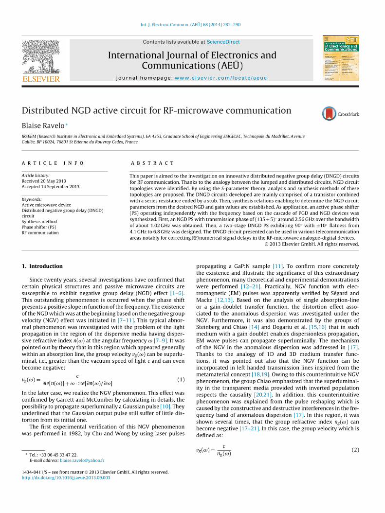
Fig. 1. Equivalence between the lumped LC network and distributed stub circuit atthe resonance.
family of DNGD active microwave circuits. It will be examinedwhen the established distributed microwave circuits exhibit NGD.Then, the synthesis relations allowing to design DNGD circuits infunction of the desired NGD, gain and matching levels will be alsointroduced. Section 3 is focused on the application of the NGD activedistributed topology for the design of independent-frequency PS.Lastly, Section 4 is the conclusion.
2. Theory of the DNGD active circuit under investigation
As illustrated in Fig. 1(a), the reactive passive network formedby LC-series is electrically equivalent to the stub or a distributedtransmission line (TL). For the simplification, the latter has a char-acteristic impedance Zc and physical length d, and quarter angularfrequency ω0.
In the remainder of this paper, this equivalence will be appliedto the NGD microwave active circuit topology in the left of Fig. 1(b)[33,34]. It is interesting to note that the NGD function is ensured bythe lumped cell mainly constituted by the shunt RLC-series passivenetwork. According to the TL theory, the input impedance of theopen-end stub line can be assumed as an inductance or capacitancein certain frequency range. So that, by considering a distributedline with characteristic impedance Zc and physical length d havingEM medium propagation speed v = c
√εr (c is the light speed in
the vacuum), the input impedance of the short-circuited and open-ended stubs are respectively written as:
Zins = j · Zc · tan
(ω · d
√εr
c
), (5)
Zino = Zc
j · tan(ω · d√
εr/c), (6)
where ω is the angular frequency.
2.1. General configuration of the DNGD circuit proposed
In order to generalize the different configurations of the DNGDactive cells, let us consider the electrical equivalence shown inFig. 1(a). This lumped circuit is equivalent to the distributed cellshown in the right of Table 1 at the resonance ω0 = 1/
√LC for cer-
tain values of charge Rl (Rl = 0 short-circuited resonant stub andRl = ∞: open-ended resonant stub). These active topologies can begeneralized by the family of circuit comprised of an FET in cascadewith shunt impedance Zin as represented in Fig. 2(a).
To simplify the analytical calculations, the FET is assumed asconsisted of a voltage-controlled current source with transcon-ductance gm in cascade with drain-source resistor Rds. The inputimpedance seen in the reference plane A–A′ of the circuit shown inFig. 2(b) is expressed as:
Zin(jω) = R + Zc
[Rl + j · Zc · tan( ̌ · d)
Zc + j · Rl · tanh( ̌ · d)
], (7)
284 B. Ravelo / Int. J. Electron. Commun. (AEÜ) 68 (2014) 282– 290
Table 1NGD microwave active circuit with lumped RLC-network and its equivalence with distributed circuit together with its S-parameters and group delay expressions.
NGD active topology S-parameters and group delay
S21[jω0(k)] = −2gmZ0RdsRlZ2c
(RRl + Z2c )(Rds + Z0) + RlRdsZ0
(11)
S22[jω0(k)] = (RRl + Z2c )(Rds − Z0) − RlRdsZ0
(RRl + Z2c )(Rds + Z0) + RlRdsZ0
(12)
�[ω0(k)] =�RdsZ0Zc(Z2
c − R2l)
2ω0(Z2c + RRl)[(RRl + Z2
c )(Rds + Z0) + RlRdsZ0](13)
wp
S
S
waStc
2l
p
ω
tia
here ̌ = ω√
εr/c represents the phase constant. The S-arameters of this NGD circuit are written as:
21(jω) = −2Z0 · gm · Rds · Zin(jω)Rds · Zin(jω) + Z0 · [Zin(jω) + Rds]
, (8)
22(jω) = Rds · Zin(jω) − Z0 · [Zin(jω) + Rds]Rds · Zin(jω) + Z0 · [Zin(jω) + Rds]
, (9)
ith Z0 is the reference impedance. In this case, the FET is supposeds unilateral. Then, the other S-parameters are equal to S11 = 1 and12 = 0. According to the behaviour of the passive network consti-uting the DNGD cell shown in Fig. 2(a), one distinguishes differentategories of NGD circuits.
.1.1. NGD cell composed of FET and an ideal line associated withumped resistances
At the quarter wavelength angular frequencies of the TL (k is aositive integer):
(k) = (1 + 4k)√
εr , (10)
0 2che transmission and reflection parameters expressed respectivelyn (8) and (9) will be transformed as expressed in (11) and (12)ddressed in Table 1. At the same frequencies, the group delay is
Fig. 2. FET in cascade with
defined in (13). One remarks that this group delay is negative underthe condition Zc < Rl. Meanwhile, the group delay is always nega-tive if the load resistance Rl is equal to ∞. This finding enables toinvestigate the circuit composed of passive network assumed as asingle lossy-line in the next subsection.
2.1.2. NGD cell composed of FET and a single lossy-lineFig. 2(b) represents the configuration of the DNGD circuit by
taking R = 0 and Rl = ∞. Knowing that coth(� · d) = 1/tanh( ̨ · d), onedemonstrates that the transmission and output reflection param-eters are expressed in (14) and (15) figured out in Table 2. Then,the corresponding group delay is written in (16). By inverting theequation
∣∣S21(jωk)∣∣ = T21, one can determine the TL parameters
indicated in (17) and (18) allowing to achieve the desired valueof gain T21. By inverting the equation �(ωk) = �, the following char-acteristic impedance expression is established in (19). In practice,the control of the TL parameters ̨ and Zc according to the desiredvalues of gain and NGD is relatively difficult. Moreover, the loss
constant ̨ is almost negligible for most of applications. To passthis ambiguous limitation, one proposes to study a distributed cellcomposed of theoretically lossless line and a resistance R in the nextsection.shunt impedance Zin .

B. Ravelo / Int. J. Electron. Commun. (AEÜ) 68 (2014) 282– 290 285
Table 2Topologies of DNGD circuits together with their corresponding analysis and synthesis expressions.
DNGD topologies Analysis and synthesis relations
S21(jωk) = −2gmRdsZ0Zc
Zc(Rds + Z0) + RdsZ0 tanh( ̨ · d)(14)
S22(jωk) = Zc(Rds − Z0) − RdsZ0 tanh( ̨ · d)Zc(Rds + Z0) + RdsZ0 tanh( ̨ · d)
(15)
�(ωk) = 2�Z0Rds/ω0
2Zc(Z0 + Rds) + [Zc(Z0 + Rds) + Z0Rds]e2˛·d
+[Zc(Z0 + Rds) − Z0Rds]e−2˛·d
(16)
Zc = T21Z0 tanh( ̨ · d)2gmRdsZ0 − T21(Rds + Z0)
(17)
˛d = arg tanh
{Zc[2gmRdsZ0 − T21(Rds + Z0)]
T21Z0
}(18)
˛d = arg tanh
{Zc[2gmRdsZ0 − T21(Rds + Z0)]
T21Z0
}(19)
S21(ωk) = −2gmRdsZ0R
R(Rds + Z0) + RdsZ0(20)
S22(ωk) = R(Rds − Z0) − RdsZ0
R(Rds + Z0) + RdsZ0(21)
�(ωk) = −�RdsZ0Zc
2Rω0 [R(Rds + Z0) + RdsZ0](22)
R =Z0Rds
∣∣S21(ω0)∣∣
2gmZ0Rds −∣∣S21(ω0)
∣∣ (Z0 + Rds)(24)
Zc = 2Rω0�(ω0)[R(Rds + Z0) + RdsZ0]−�RdsZ0
(25)
Zc = 2Rω0�(ω0)[R(Rds + Z0) + RdsZ0]−�RdsZ0
(27)
� [ω0(k)] = −d · RdsZ0Zc
vR[RRds + Z0(R + Rds)]= −�RdsZ0Zc
2ω0R[RRds + Z0(R + Rds)](29)
R =
∣∣S21(0)∣∣RdsZ0
2gmRdsZ0 −∣∣S21(0)
∣∣ (Z0 + Rds)(31)
Zc = −vR�(0)[RRds + Z0(R + Rds)]dRdsZ0
(32)
2s
scZ
e
.1.3. NGD cell composed of FET and open-ended lossless-line ineries with a resistance
Fig. 2(c) of Table 2 represents the DNGD circuit under con-ideration which is constituted by an open-ended TL. In this
ase, the input impedance seen in the plane A–A′ is equal toin = R + j · Zccoth(2ˇ · d).The S-parameters and the group delay are respectivelyxpressed in (20), (21) and (22). The group delay of this circuit is
negative in the periodical frequency bands [ωc(k), ωc(k + 1)] definedby the following equation:
[�ωc(k)
] Zc
√R(Rds + Z0)[R(Rds + Z0) + RdsR]
tan2ω0
− k� =R[R(Rds + Z0) + RdsR]
. (23)
By taking ω0(k) → ω0(0) = ω0, one deduces from (20)and (22), synthesis relations (24) and (25). To achieve a
286 B. Ravelo / Int. J. Electron. Commun
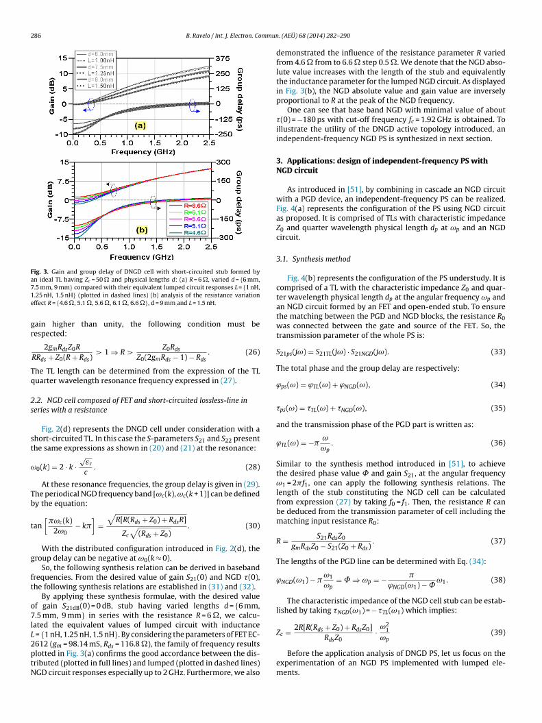
Fig. 3. Gain and group delay of DNGD cell with short-circuited stub formed byan ideal TL having Zc = 50 � and physical lengths d: (a) R = 6 �, varied d = {6 mm,71e
gr
Tq
2s
st
ω
Tb
t
g
ft
o7lL2ptN
p
.5 mm, 9 mm} compared with their equivalent lumped circuit responses L = {1 nH,
.25 nH, 1.5 nH} (plotted in dashed lines) (b) analysis of the resistance variationffect R = {4.6 �, 5.1 �, 5.6 �, 6.1 �, 6.6 �}, d = 9 mm and L = 1.5 nH.
ain higher than unity, the following condition must beespected:
2gmRdsZ0R
RRds + Z0(R + Rds)> 1 ⇒ R >
Z0Rds
Z0(2gmRds − 1) − Rds. (26)
he TL length can be determined from the expression of the TLuarter wavelength resonance frequency expressed in (27).
.2. NGD cell composed of FET and short-circuited lossless-line ineries with a resistance
Fig. 2(d) represents the DNGD cell under consideration with ahort-circuited TL. In this case the S-parameters S21 and S22 presenthe same expressions as shown in (20) and (21) at the resonance:
0(k) = 2 · k ·√
εr
c. (28)
At these resonance frequencies, the group delay is given in (29).he periodical NGD frequency band [ωc(k), ωc(k + 1)] can be definedy the equation:
an[
�ωc(k)2ω0
− k�]
=√
R[R(Rds + Z0) + RdsR]
Zc
√(Rds + Z0)
. (30)
With the distributed configuration introduced in Fig. 2(d), theroup delay can be negative at ω0(k ≈ 0).
So, the following synthesis relation can be derived in basebandrequencies. From the desired value of gain S21(0) and NGD �(0),he following synthesis relations are established in (31) and (32).
By applying these synthesis formulae, with the desired valuef gain S21dB(0) = 0 dB, stub having varied lengths d = {6 mm,.5 mm, 9 mm} in series with the resistance R = 6 �, we calcu-
ated the equivalent values of lumped circuit with inductance = {1 nH, 1.25 nH, 1.5 nH}. By considering the parameters of FET EC-
612 (gm = 98.14 mS, Rds = 116.8 �), the family of frequency resultslotted in Fig. 3(a) confirms the good accordance between the dis-ributed (plotted in full lines) and lumped (plotted in dashed lines)GD circuit responses especially up to 2 GHz. Furthermore, we also. (AEÜ) 68 (2014) 282– 290
demonstrated the influence of the resistance parameter R variedfrom 4.6 � from to 6.6 � step 0.5 �. We denote that the NGD abso-lute value increases with the length of the stub and equivalentlythe inductance parameter for the lumped NGD circuit. As displayedin Fig. 3(b), the NGD absolute value and gain value are inverselyproportional to R at the peak of the NGD frequency.
One can see that base band NGD with minimal value of about�(0) = −180 ps with cut-off frequency fc = 1.92 GHz is obtained. Toillustrate the utility of the DNGD active topology introduced, anindependent-frequency NGD PS is synthesized in next section.
3. Applications: design of independent-frequency PS withNGD circuit
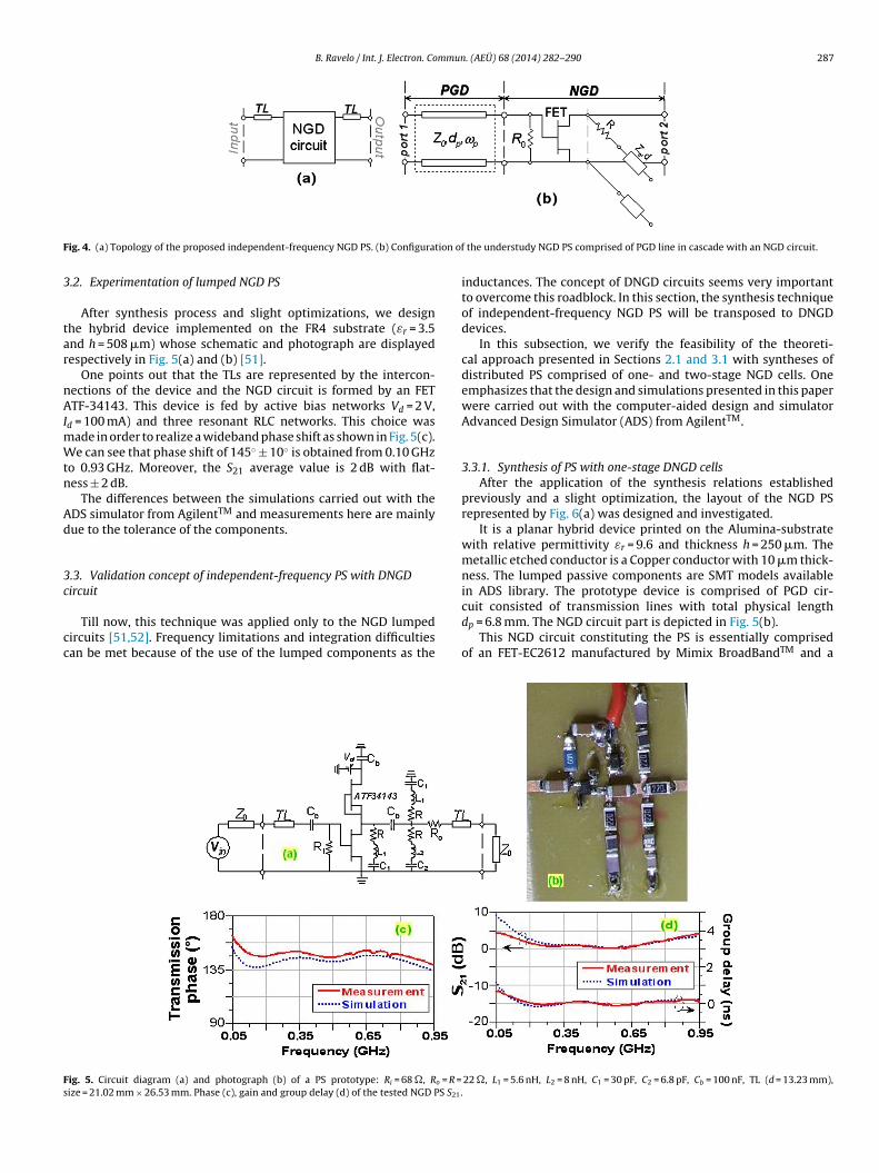
As introduced in [51], by combining in cascade an NGD circuitwith a PGD device, an independent-frequency PS can be realized.Fig. 4(a) represents the configuration of the PS using NGD circuitas proposed. It is comprised of TLs with characteristic impedanceZ0 and quarter wavelength physical length dp at ωp and an NGDcircuit.
3.1. Synthesis method
Fig. 4(b) represents the configuration of the PS understudy. It iscomprised of a TL with the characteristic impedance Z0 and quar-ter wavelength physical length dp at the angular frequency ωp andan NGD circuit formed by an FET and open-ended stub. To ensurethe matching between the PGD and NGD blocks, the resistance R0was connected between the gate and source of the FET. So, thetransmission parameter of the whole PS is:
S21ps(jω) = S21TL(jω) · S21NGD(jω). (33)
The total phase and the group delay are respectively:
ϕps(ω) = ϕTL(ω) + ϕNGD(ω), (34)
�ps(ω) = �TL(ω) + �NGD(ω), (35)
and the transmission phase of the PGD part is written as:
ϕTL(ω) = −�ω
ωp. (36)
Similar to the synthesis method introduced in [51], to achievethe desired phase value ̊ and gain S21, at the angular frequencyω1 = 2�f1, one can apply the following synthesis relations. Thelength of the stub constituting the NGD cell can be calculatedfrom expression (27) by taking f0 = f1. Then, the resistance R canbe deduced from the transmission parameter of cell including thematching input resistance R0:
R = S21RdsZ0
gmRdsZ0 − S21(Z0 + Rds). (37)
The lengths of the PGD line can be determined with Eq. (34):
ϕNGD(ω1) − �ω1
ωp= ̊ ⇒ ωp = − �
ϕNGD(ω1) − ˚ω1. (38)
The characteristic impedance of the NGD cell stub can be estab-lished by taking �NGD(ω1) = − �TL(ω1) which implies:
Zc = 2R[R(Rds + Z0) + RdsZ0]R Z
· ω21
ω(39)
ds 0
Before the application analysis of DNGD PS, let us focus on theexperimentation of an NGD PS implemented with lumped ele-ments.
B. Ravelo / Int. J. Electron. Commun. (AEÜ) 68 (2014) 282– 290 287
F tion of
3
tar
nAImWtn
Ad
3c
cc
Fs
ig. 4. (a) Topology of the proposed independent-frequency NGD PS. (b) Configura
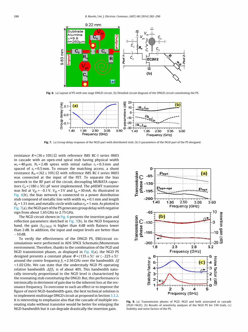
.2. Experimentation of lumped NGD PS
After synthesis process and slight optimizations, we designhe hybrid device implemented on the FR4 substrate (εr = 3.5nd h = 508 �m) whose schematic and photograph are displayedespectively in Fig. 5(a) and (b) [51].
One points out that the TLs are represented by the intercon-ections of the device and the NGD circuit is formed by an FETTF-34143. This device is fed by active bias networks Vd = 2 V,
d = 100 mA) and three resonant RLC networks. This choice wasade in order to realize a wideband phase shift as shown in Fig. 5(c).e can see that phase shift of 145◦ ± 10◦ is obtained from 0.10 GHz
o 0.93 GHz. Moreover, the S21 average value is 2 dB with flat-ess ± 2 dB.
The differences between the simulations carried out with theDS simulator from AgilentTM and measurements here are mainlyue to the tolerance of the components.
.3. Validation concept of independent-frequency PS with DNGDircuit
Till now, this technique was applied only to the NGD lumpedircuits [51,52]. Frequency limitations and integration difficultiesan be met because of the use of the lumped components as the
ig. 5. Circuit diagram (a) and photograph (b) of a PS prototype: Ri = 68 �, Ro = R =ize = 21.02 mm × 26.53 mm. Phase (c), gain and group delay (d) of the tested NGD PS S21.
the understudy NGD PS comprised of PGD line in cascade with an NGD circuit.
inductances. The concept of DNGD circuits seems very importantto overcome this roadblock. In this section, the synthesis techniqueof independent-frequency NGD PS will be transposed to DNGDdevices.
In this subsection, we verify the feasibility of the theoreti-cal approach presented in Sections 2.1 and 3.1 with syntheses ofdistributed PS comprised of one- and two-stage NGD cells. Oneemphasizes that the design and simulations presented in this paperwere carried out with the computer-aided design and simulatorAdvanced Design Simulator (ADS) from AgilentTM.
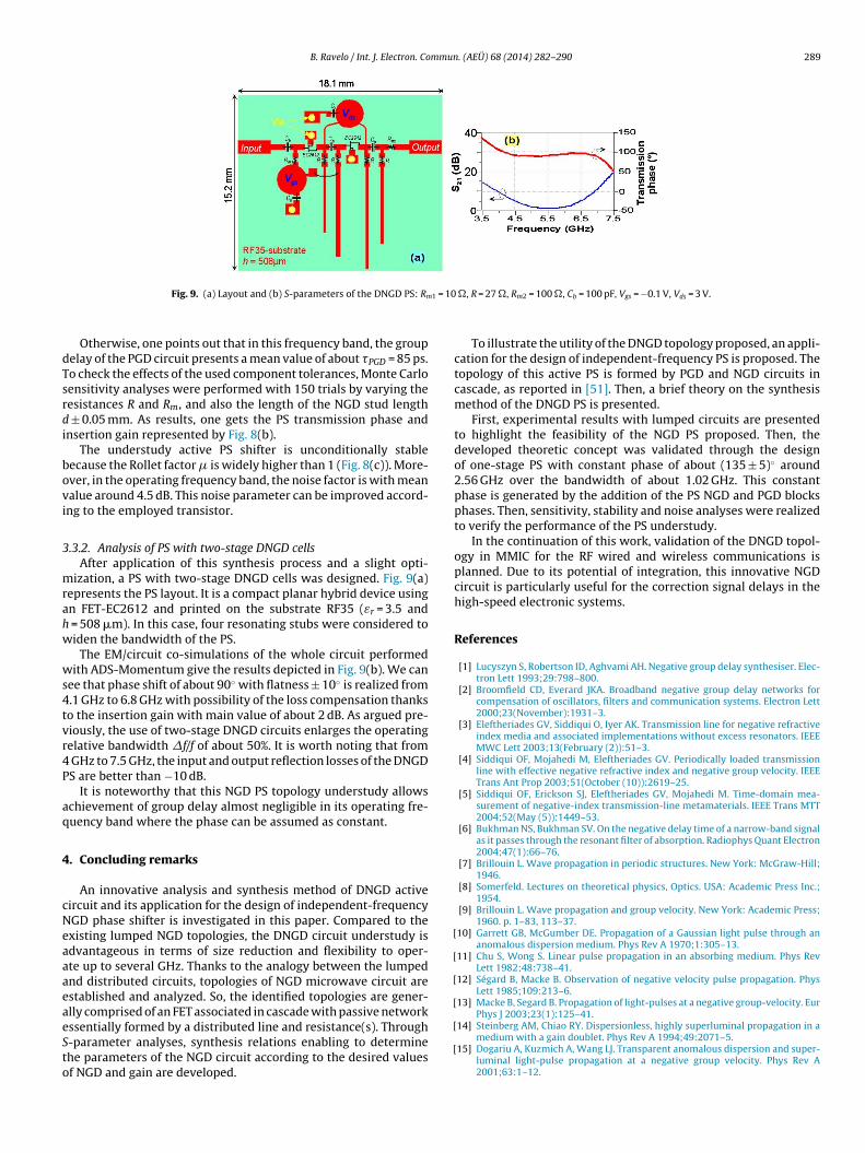
3.3.1. Synthesis of PS with one-stage DNGD cellsAfter the application of the synthesis relations established
previously and a slight optimization, the layout of the NGD PSrepresented by Fig. 6(a) was designed and investigated.
It is a planar hybrid device printed on the Alumina-substratewith relative permittivity εr = 9.6 and thickness h = 250 �m. Themetallic etched conductor is a Copper conductor with 10 �m thick-ness. The lumped passive components are SMT models availablein ADS library. The prototype device is comprised of PGD cir-
cuit consisted of transmission lines with total physical lengthdp = 6.8 mm. The NGD circuit part is depicted in Fig. 5(b).This NGD circuit constituting the PS is essentially comprisedof an FET-EC2612 manufactured by Mimix BroadBandTM and a
22 �, L1 = 5.6 nH, L2 = 8 nH, C1 = 30 pF, C2 = 6.8 pF, Cb = 100 nF, TL (d = 13.23 mm),
288 B. Ravelo / Int. J. Electron. Commun. (AEÜ) 68 (2014) 282– 290
Fig. 6. (a) Layout of PS with one stage DNGD circuit. (b) Detailed circuit diagram of the DNGD circuit constituting the PS.
ibuted stub. (b) S-parameters of the NGD part of the PS designed.
riwsrwniwFsdFs
rbt−
seNda≈rrtiofitIoN
Fig. 7. (a) Group delay response of the NGD part with distr
esistance R = (36 ± 10%) � with reference IMS RC-I series 0603n cascade with an open-end spiral stub having physical width
s = 40 �m, Ns = 2.48 spires with initial radius rs = 0.3 mm andpaced of ss = 0.5 mm. To ensure the matching access, a shuntesistance Rm = (62 ± 10%) � with reference IMS RC-I series 0603as connected at the input of the FET. To separate the biasetwork to the RF part of the circuit, decoupling MURATA capac-
tors Cb = (180 ± 5%) pF were implemented. The pHEMT transistoras fed at Vgs = −0.1 V, Vds = 3 V and Ids = 30 mA. As illustrated in
ig. 6(b), the bias network is connected to a power distributiontub composed of metallic line with width wb = 0.1 mm and lengthb = 1.51 mm, and metallic circle with radius rb = 1 mm. As plotted inig. 7(a), the NGD part of the PS generates group delay with negativeign from about 1.65 GHz to 2.75 GHz.
The NGD circuit shown in Fig. 6 presents the insertion gain andeflection parameters sketched in Fig. 7(b). In the NGD frequencyand, the gain |S21|NGD is higher than 4 dB with flatness lowerhan 2 dB. In addition, the input and output levels are better than10 dB.
To verify the effectiveness of the DNGD PS, EM/circuit co-imulations were performed in ADS SPICE Schematic/Momentumnvironment. Therefore, thanks to the combination of the PGD andGD transmission phases, as displayed in Fig. 8(a), the NGD PSesigned presents a constant phase ̊ = (135 ± 5)◦ or (−225 ± 5)◦
round the centre frequency f1 = 2.56 GHz over the bandwidth f1.02 GHz. We can state that the understudy NGD PS operating
elative bandwidth f/f1 is of about 40%. This bandwidth natu-ally inversely proportional to the NGD level is characterized byhe resonating stub constituting the DNGD. But, this performance isntrinsically in detriment of gain due to the inherent loss at the res-nance frequency. To overcome to such an effect or to improve thegure of merit NGD-bandwidth-gain, the best technical solution is
o implement multistage DNGD circuit as proposed in Section 3.3.2.t is interesting to emphasize also that the cascade of multiple res-nating stubs without transistor would be better for enlarging theGD bandwidth but it can degrade drastically the insertion gain.Fig. 8. (a) Transmission phases of PGD, NGD and both associated in cascade(PGD + NGD). (b) Results of sensitivity analyses of the NGD PS for 150 trials. (c)Stability and noise factors of the PS.
B. Ravelo / Int. J. Electron. Commun. (AEÜ) 68 (2014) 282– 290 289
1 = 10
dTsrdi
bovi
3
mrahw
ws4tvr4P
aq
4
cNeaaaeaeSto
[
[
[
[
Fig. 9. (a) Layout and (b) S-parameters of the DNGD PS: Rm
Otherwise, one points out that in this frequency band, the groupelay of the PGD circuit presents a mean value of about �PGD = 85 ps.o check the effects of the used component tolerances, Monte Carloensitivity analyses were performed with 150 trials by varying theesistances R and Rm, and also the length of the NGD stud length
± 0.05 mm. As results, one gets the PS transmission phase andnsertion gain represented by Fig. 8(b).
The understudy active PS shifter is unconditionally stableecause the Rollet factor � is widely higher than 1 (Fig. 8(c)). More-ver, in the operating frequency band, the noise factor is with meanalue around 4.5 dB. This noise parameter can be improved accord-ng to the employed transistor.
.3.2. Analysis of PS with two-stage DNGD cellsAfter application of this synthesis process and a slight opti-
ization, a PS with two-stage DNGD cells was designed. Fig. 9(a)epresents the PS layout. It is a compact planar hybrid device usingn FET-EC2612 and printed on the substrate RF35 (εr = 3.5 and
= 508 �m). In this case, four resonating stubs were considered toiden the bandwidth of the PS.
The EM/circuit co-simulations of the whole circuit performedith ADS-Momentum give the results depicted in Fig. 9(b). We can
ee that phase shift of about 90◦ with flatness ± 10◦ is realized from.1 GHz to 6.8 GHz with possibility of the loss compensation thankso the insertion gain with main value of about 2 dB. As argued pre-iously, the use of two-stage DNGD circuits enlarges the operatingelative bandwidth f/f of about 50%. It is worth noting that from
GHz to 7.5 GHz, the input and output reflection losses of the DNGDS are better than −10 dB.
It is noteworthy that this NGD PS topology understudy allowschievement of group delay almost negligible in its operating fre-uency band where the phase can be assumed as constant.
. Concluding remarks
An innovative analysis and synthesis method of DNGD activeircuit and its application for the design of independent-frequencyGD phase shifter is investigated in this paper. Compared to thexisting lumped NGD topologies, the DNGD circuit understudy isdvantageous in terms of size reduction and flexibility to oper-te up to several GHz. Thanks to the analogy between the lumpednd distributed circuits, topologies of NGD microwave circuit arestablished and analyzed. So, the identified topologies are gener-lly comprised of an FET associated in cascade with passive network
ssentially formed by a distributed line and resistance(s). Through-parameter analyses, synthesis relations enabling to determinehe parameters of the NGD circuit according to the desired valuesf NGD and gain are developed.[
[
�, R = 27 �, Rm2 = 100 �, Cb = 100 pF, Vgs = −0.1 V, Vds = 3 V.
To illustrate the utility of the DNGD topology proposed, an appli-cation for the design of independent-frequency PS is proposed. Thetopology of this active PS is formed by PGD and NGD circuits incascade, as reported in [51]. Then, a brief theory on the synthesismethod of the DNGD PS is presented.
First, experimental results with lumped circuits are presentedto highlight the feasibility of the NGD PS proposed. Then, thedeveloped theoretic concept was validated through the designof one-stage PS with constant phase of about (135 ± 5)◦ around2.56 GHz over the bandwidth of about 1.02 GHz. This constantphase is generated by the addition of the PS NGD and PGD blocksphases. Then, sensitivity, stability and noise analyses were realizedto verify the performance of the PS understudy.
In the continuation of this work, validation of the DNGD topol-ogy in MMIC for the RF wired and wireless communications isplanned. Due to its potential of integration, this innovative NGDcircuit is particularly useful for the correction signal delays in thehigh-speed electronic systems.
References
[1] Lucyszyn S, Robertson ID, Aghvami AH. Negative group delay synthesiser. Elec-tron Lett 1993;29:798–800.
[2] Broomfield CD, Everard JKA. Broadband negative group delay networks forcompensation of oscillators, filters and communication systems. Electron Lett2000;23(November):1931–3.
[3] Eleftheriades GV, Siddiqui O, Iyer AK. Transmission line for negative refractiveindex media and associated implementations without excess resonators. IEEEMWC Lett 2003;13(February (2)):51–3.
[4] Siddiqui OF, Mojahedi M, Eleftheriades GV. Periodically loaded transmissionline with effective negative refractive index and negative group velocity. IEEETrans Ant Prop 2003;51(October (10)):2619–25.
[5] Siddiqui OF, Erickson SJ, Eleftheriades GV, Mojahedi M. Time-domain mea-surement of negative-index transmission-line metamaterials. IEEE Trans MTT2004;52(May (5)):1449–53.
[6] Bukhman NS, Bukhman SV. On the negative delay time of a narrow-band signalas it passes through the resonant filter of absorption. Radiophys Quant Electron2004;47(1):66–76.
[7] Brillouin L. Wave propagation in periodic structures. New York: McGraw-Hill;1946.
[8] Somerfeld. Lectures on theoretical physics, Optics. USA: Academic Press Inc.;1954.
[9] Brillouin L. Wave propagation and group velocity. New York: Academic Press;1960. p. 1–83, 113–37.
10] Garrett GB, McGumber DE. Propagation of a Gaussian light pulse through ananomalous dispersion medium. Phys Rev A 1970;1:305–13.
11] Chu S, Wong S. Linear pulse propagation in an absorbing medium. Phys RevLett 1982;48:738–41.
12] Ségard B, Macke B. Observation of negative velocity pulse propagation. PhysLett 1985;109:213–6.
13] Macke B, Segard B. Propagation of light-pulses at a negative group-velocity. EurPhys J 2003;23(1):125–41.
14] Steinberg AM, Chiao RY. Dispersionless, highly superluminal propagation in amedium with a gain doublet. Phys Rev A 1994;49:2071–5.
15] Dogariu A, Kuzmich A, Wang LJ. Transparent anomalous dispersion and super-luminal light-pulse propagation at a negative group velocity. Phys Rev A2001;63:1–12.

2 mmun
[
[[
[
[
[
[
[
[
[
[
[
[
[
[
[
[
[
[
[
[
[
[
[[
[
[
[
[
[
[
[
[
[
[
[
90 B. Ravelo / Int. J. Electron. Co
16] Wang LJ, Kuzmich A, Dogariu A. Gain-assisted superluminal light propagation.Nature 2000;406:277–9.
17] McDonald KT. Negative group velocity. Am J Physiol 2001;69(May (5)):607–14.18] Siddiqui OF, Mojahedi M, Eleftheriades GV. Periodically loaded transmission
line with effective negative refractive index and negative group velocity. IEEETran Ant Prop 2003;51(October (10)):2619–25.
19] Woodley JF, Mojahedi M. Negative group velocity and group delay in left-handed media. Phys Rev E 2004;70:1–6.
20] Chiao RY. Superluminal (but causal) propagation of wave packets in transparentmedia with inverted atomic populations. Phys Rev A 1993;48:R34–7.
21] Chiao RY. Population inversion and superluminality. In: Amazing light. NewYork: Springer-Verlag; 1996. p. 91–108.
22] Chiao RY, Bolda EL, Bowie J, Boyce J, Mitchell MW. Superluminality and ampli-fiers. Prog Cryst Growth Charact Mater 1996;33:319–25.
23] Mitchell MW, Chiao RY. Causality and negative group delays in a simple band-pass amplifier. Am J Physiol 1998;66:14–9.
24] Mitchell MW, Chiao RY. Negative group delay and ‘fronts’ in a causal sys-tems: an experiment with very low frequency bandpass amplifiers. Phys LettA 1997;230(June):133–8.
25] Solli D, Chiao RY, Hickmannn JM. Superluminal effects and negative groupdelays in electronics, and their applications. Phys Rev E 2002;66:1–4.
26] Nakanishi T, Sugiyama K, Kitano M. Demonstration of negative group delays ina simple electronic circuit. Am J Physiol 2002;70(11):1117–21.
27] Kitano M, Nakanishi T, Sugiyama K. Negative group delay and superluminalpropagation: an electronic circuit approach. IEEE J Sel Top Quant Electron2003;9(February (1)):43–51.
28] Munday JN, Henderson RH. Superluminal time advance of a complex audiosignal. Appl Phys Lett 2004;85(July):503–4.
29] Erickson SJ, Khaja M, Mojahedi M. Time- and frequency-domain measurementsfor an active negative group delay circuit. In: Proceedings of IEEE antennapropagation society international symposium, vol. 3A. 2005. p. 790–3.
30] Munday JN, Robertson WM. Observation of negative group delays within acoaxial photonic crystal using an impulse response method. Opt Commun2007;273(1):32–6.
31] Ravelo B. Methodology of elementary NGD active topologies identification. IETCircuits Devices Syst 2013:1–9, http://dx.doi.org/10.1049/iet-cds.2012.0317.
32] Ravelo B. Similitude between the NGD and filter gain behaviors. Int J Circ TheorAppl 2013;(March):1–17, http://dx.doi.org/10.1002/cta.1902.
33] Ravelo B. Investigation on microwave negative group delay circuit. Electromag-netics 2011;31(November (8)):537–49.
34] Ravelo B, De Blasi S. An FET-based microwave active circuit with dual-band negative group delay. J Microw Optoelectron Electromagnet Appl2011;10(December (2)):355–66.
35] Ravelo B. Baseband NGD circuit with RF amplifier. Electron Lett 2011;47(June(13)):752–4.
[
. (AEÜ) 68 (2014) 282– 290
36] Kandic M, Bridges GE. Transient-imposed limitations of negative group delaycircuits. In: Proceedings of 14th international symposium ANTEM-AMEREMconference. 2010. p. 1–4.
37] Kandic M, Bridges GE. Asymptotic limits of negative group delay inactive resonator-based distributed circuits. IEEE Trans CAS I: Regul Pap2011;58(August (8)):1727–35.
38] Ravelo B. Delay modelling of high-speed distributed interconnect for the signalintegrity prediction. Eur Phys J Appl Phys 2012;57(February):1–8.
39] White P. Group delay explanations and applications. Appl Radio Labs 1999:1–6.40] Abate Z. WiMAX RF systems engineering. Mobile communication series. Nor-
wood, MA, USA: Artech House; 2009.41] Mumford R. European carriers face capacity crunch challenges. Int Rep
Microwave J 2010;(April):169–70.42] Myoung S-S, Kwon B-S, Kim Y-H, Yook J-G. Effect of group delay in RF BPF on
impulse radio systems. IEICE Trans Commun 2007;90(12):3514–22.43] Gupta S, Parsa A, Perret E, Snyder RV, Wenzel RJ, Caloz C. Group-delay engi-
neered noncommensurate transmission line all-pass network for analog signalprocessing. IEEE Trans MTT 2010;58(December (9)):2392–407.
44] Ravelo B, Ben Hadj Slama J. Equalization of digital/mixed-signal disturbanceswith an negative group delay circuit. In: Proceedings of 16th IEEE MELECON,Medine Yasmine Hammamet, 25–28 March. 2012. p. 844–7.
45] Ravelo B, Liu Y. Microwave/digital signal correction with integrable NGD cir-cuits. In: Proceedings of 2012 IEEE MTT-S international microwave symposiumdigest. 2012. p. 1–3.
46] Ahn K-P, Ishikawa R, Honjo K. Group delay equalized UWB InGaP/GaAsHBT MMIC amplifier using negative group delay circuits. IEEE Trans MTT2009;57(September (9)):2139–47.
47] Podilchak SK, Frank BM, Freundorfer AP, Antar YMM. High speed metamaterial-inspired negative group delay circuits in CMOS for delay equalization. In:Proceedings of 2nd Microsystems and Nanoelectronics Research Conference.2009. p. 9–12.
48] Noto H, Yamauchi K, Nakayama M, Isota Y. Negative group delay circuit forfeed-forward amplifier. IEEE Int Microw Symp Dig 2007;(June):1103–6.
49] Choi H, Jeong Y, Kim CD, Kenney JS. Bandwidth enhancement of an analog feed-back amplifier by employing a negative group delay circuit. Prog ElectromagnetRes 2010;105:253–72.
50] Choi H, Jeong Y, Kim CD, Kenney JS. Efficiency enhancement of feedfor-ward amplifiers by employing a negative group-delay circuit. IEEE Trans MTT2010;58(May (5)):1116–25.
51] Ravelo B. In: Etomsa GmbH., Co K.G., editors. Theory and design of analogue and
numerical elementary NGD circuits: theoretical characterization of analogueand numerical elementary NGD circuits. Chapter 10. Sarrebruck, Germany: LAPLambert Academic Publishing; 2012. March.52] Keser S, Mojahedi M. Broadband negative group delay microstrip phase shifterdesign. In: Proceedings of IEEE APSURSI’09. 2009. p. 1–4.