Embed Size (px)
Citation preview

I
AD-769 585
DESIGN AND ANALYSIS OF 90-DEGREE PHASE
DIFFERENCE NETWORKS
W. Wiebach
Harry Diamond LaboratoriesWashington, D. C.
May 1973
DISTRIBUTED BY:
National Technical Information ServiceU. S. DEPARTMENT OF COMMERCE5285 Pori Royal-Road, Springfield Va. 22151

Ii NC LASSIFIEDSecurity C0,.3ificatior.
DOCUMENT CONTR~OL DATA.- R & D
I oflCimAINI: ACTIVITY (Co~,cafe auho) 2& flRsC~jntry CLAISIFICATION
Harr DiaondLaboatores b. CROUP
DESIGN & ANALYSIS OF 90 DEGREE PHASE DIFFERENCE NETWORK
4. CEsctIPTIve tdoTas (?'pt of report and Incte.Ie, date#)
S. AU 1"4OR4') (First (141M, xr~ddlo intticI Moct naome)
W. Wiebach
June 197:3 D ~ RGNtRSRPR
(his report)
APPRVEDFORPUBIC RLEAE; ORMAUT N SERVICE ED
U~U S. Armyi~vn Maere Command
IS. AOSTRACT
R!PLAUU NFORM 47. AT4IN SRICE
DI .. 17 .,* OS0O-STU VO* ARMY U12. UC&SFE
Security Closelicetion

UNCLASSIFIED£ SoCurity CZlasfifcation
_4 LINKA L IKa LINK C
Differenve
Network
UNi LASSJYJ'EDS~ccwity CLSM1ication

ABISTRACT
The parameters or a 9O-degrec- [)hsc difference (Dome) filter, and theirrelationship to the filter chara ecris ties, a ce derived and discussed. The dcsignof two RC impleentfatiois and their worst- ?ase analyses a.,e shown.
:3

TABLE OF CONTENTS
Section Title Page
ABSTRACT 2.................................. 2
1 INTRODUC TION ............................... 7
2 OBJECTIVE o) THfS REPORT ......................... 8
3 DERIVAT:ON OF THE FILTER PARAMETERS ............ 9
3.1 lrequearhy -Response of the Phase Anglo ............. 93.2 Condit'n or Equal Maxihaa ..... .................. 123.3 Conditions for Equa! Ripple Around 90 Degrees ..... 153.4 Bandwidth.. ........... 153.5 Filter Parameters for a Specified Bandwi ith........... 173.6 Filter Parameters for a Specified Deviation ....... 18
4 RC REAIJZATION WITH BALANCED GENERATOR ....... 22
4.1 All-pass Conditions ........................ 224.2 Dimensioning .............................. 244.3 Effect of Component Tolerances .................... 264.4 Amplifier Considerations ...................... 284.5 Example . ............................... 30
5 RC REALIZATION WITH DTFFERENTIAL AMPLIFIER 35
5.1 All-pass Condition ......................... 365.2 Dimensioning.............................. 375.3 Effect of Component Tolerances ................ 385.4 Example ............................... 38
6 SUMMARY ........ .............................. 39
LITERATU RE CITED ............................ 43
APPENDIX I ................................. 45
APPENDTX 2. .................................
APPENDIX 3 ........................... 53
DISTRIBUTION IST ........ ........... . ....... 55
p
_rrPrcdn pg ln

LIST OF ILLUSTRATIONS
Figure Tte Page
1 Phase response versus frequency obtained withI me's Dimensionhx" ........................... 7
2 Equal-ripple phase response ......................... 7" Poles and zeros of second-degree all-pass ............. 9
4 Basic dome filter ... ........................... .. 125 Phase shift and pnase difierence of an arbitrary dome filter.. 136 Frequency finction z ................................ 137 Definition of edge frequencies fl, f 2 .................. 168 Order of calculation, and equations used, when the band
edges are specified ................................. 189 Order of calculation, and equations used, when the mximurn
deviation is specified ....... 20
10 Pole and zero locato-, for.. > 2 ...................... 2011 All-pass circuit with balanco d generator ............... 2112 Possible circuit paameter for s = 4 ............. 2513 Dome filter fed by simple ph-ise splitter, not recommended . 2914 Dome filter fed bv two transistors ................... 2915 Dome filter fed by two -operational amplifiers ........... 3016 Basic all--.ass network .......................... 3517 Sebol's all-pass circuit ................... 351.8 Solutions of r, k vs c fors=4...................... 37
LIST OF TABLES
Table Title Page
I Drive Circuit With Bandwidth Generator .............. 33II Dome Effect With Differential Amplifier .............. 40
Computer Program For the Worst Case Analysis of theDome Filter Circuit With Balanced Generator ........... 46Subprogram ARCT Required By Programs in AppendixesAppendixes 1 and 2 .......... .................. 49Computer Program For the Worst Case Analysis of theDome Filt tr Circuit With Operational Amplifier ......... 52
}-6
I . . . . = w m mm a m~mu
1. INTRODUCTION
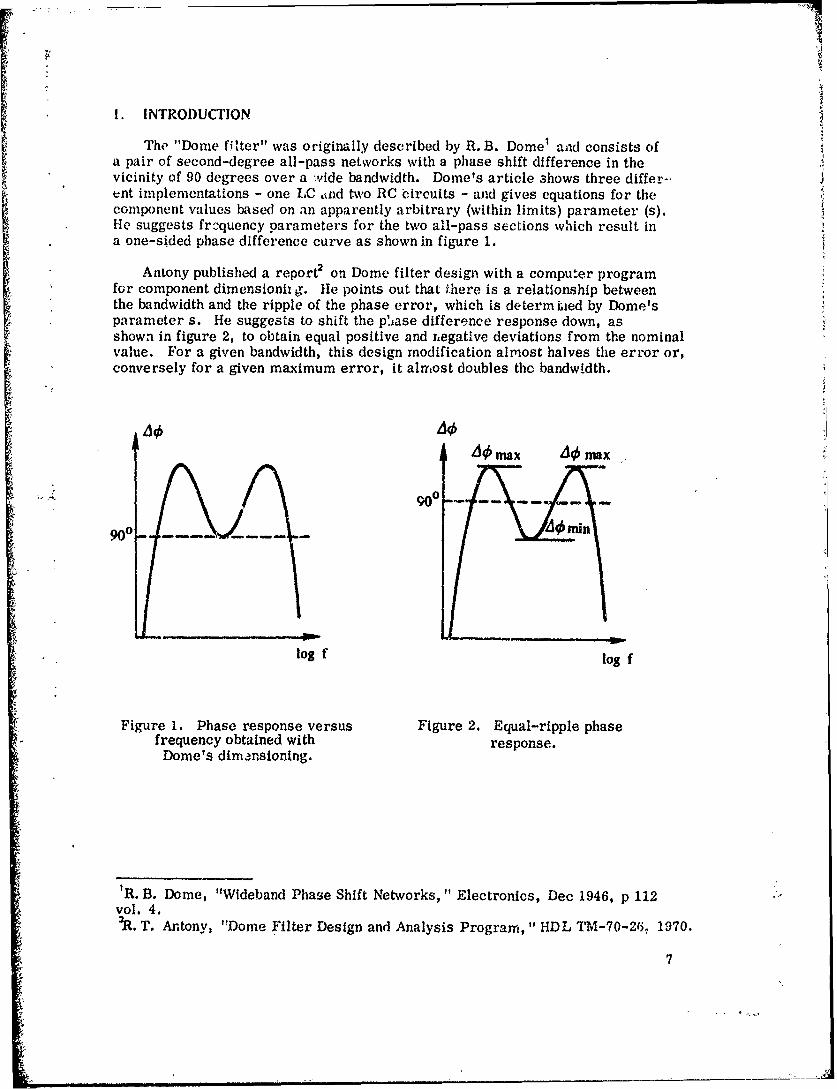
The "Dome filter" was originally described by R.B. Dome' ald consists ofa pair of second-degree all-pass networks with a phase shift difference in thevicinity of 90 degrees over a vide bandwidth. Dome's article shows three differ-.ent implementations - one LC mid two RC bircuits - and gives equations for thecomponent values based on in apparently arbitrary (within limits) parameter (s).He suggests frequency parameters for the two all-pass sections which result ina one-sided phase difference curve as shown in figure 1.
Antony published a report2 on Dome filter design with a computer programfor component dimensionih j. lie points out that there is a relationship betweenthe bandwidth and the ripple of the phase error, which is determ i~ied by Dome'sparameter s. He suggests to shift the phase difference response down, asshown in figure 2, to obtain equal positive and regative deviations from the nominalvalue. For a given bandwidth, this design modification almost halves the error or,conversely for a given maximum error, it almost doubles the bandwidth.
4#max emx
A - -900
900- --- ii
log f log f
Figure 1. Phase response versus Figure 2. Equal-ripple phasefrequency obtained with response.Dome's dimensioning.
1R. B. Dome, "Wideband Phase Shift Networks," Electronics, Dec 1946, p 112vol. 4.2R. T. A.ntony, "Dome Filter Design and Analysis Program," HDL TM-70-26: 1970.
7

Another RC realization of the Dome filter with a differential amplifier wasgiven by Sebol. He use, as filter parameters tabulated data published byBedrosian, 4 which also permit the design of higher order phase difference net-works by cascading second-degree all-pass sections. The phase responsecorresponds to figure 2.
2. OBJECTIVE OF THIS REPORT
Neither one of the cited papers presents much of the theoretical backgroundof the Dome filter, the knowledge and understanding of which can add signifi-cantly to the designer's confidence. This is one gap which this report intendsto fill. While the higher-order filters are not accessible by elementary analy-sis, the second order (Dome) filter is readily so.
The cited papers present various graphs showing the relationship betweenthe filter parameters, bandwidth and ripple; Antony's computer program calcu-lates the component values from the phase deviation.* This report derives thecalculation of the filter parameters based, at the designer's choice, either onthe required bandwidth or on the permissible phase error. It also shows theflexibility which exists in dimensioning component values.
Dome uses an arbitrary capacitance ratio in his formulas for the compon-ent values, but deprives the designer of one degree of freedom. Antony usesthis capacitance ratio in his computer program. Also, the user of his programseems to have little choice as to the component determining the impedance levelof the fil.-r. However, as this paper shows, any component of a filter sectionmay be seiz.ted for this purpose, and the impedance of the two sections neednot necessarily loc the same. It is deemed impor:ant to acquaint the designerwith the flexibility avdailble in this circuit so that he may realize it with as lowan impedance spread as possible and as many as possible standard values for thecapacitors, because non-standard capacito.:s -,;.,e expensive and hard to get.
The calculation of the component values for Sebol's circuit is also summa-rized to make it available to the user in the same frame of reference.
As this paper shows, the calcti.ation method for filter parameters and com-ponrmts, even with the described full flexibility, is not unduly complicated,requiring only a desk calculator.
Finally, this report presents worst-case analyses of the effects of compon-ent zolerances on the phase difference for a Dome circuit and the Sebol circuit.Computer programs for this purpose, and representative sample outputs arelisted.
Sebol, R., "Design of Active 90-Degree Phase Difference Networks,"HI L-TM-68-184Bedrosian, S.D., "Normalized Design of 90-Degree Phase DifferenceNetworks," IRE Trans. on r'frzuit Theory, June 1960.
*With some error: in one particular case the component values from the
computer prcgram were up to three percent off.
5a

F3. DERIVATION OF THE FILTER PARAMETERS
A
3. 1 Fre~quency Response of the Phase un io
The transfer function of a seconcJ-degree all-pass network with the complexfrequency p is (fig. 3)5
V2(p) (p .4 p 1) (p 4, T )V (p pl ) (p__-1_ (1)
Where p, 1 : ig j jp'.T
It has two conjugate-complex poles and two conjugate-complex zeros locatedsymmetrically to the poles with~ respect to both the origin and j-axis. The :
frequency response can be written as
v2(-) - +j(+][-a + j o-13)](2)
g..-" Magn.
P3 x -4
ix o-p!
Figure 3. Poles and zeros of second-degree all-p., ss.
see, for instance, L. Weinberg, "Network Analysis and Synthesis, McGrawWill 19612, p 2A5.
9

with the phase angle : 1 2 3 4
The phase angles of the individual terms are expressed by
tanO, - .
a
tan4,4 -a
_'--nO- tan .-
-a
* -2 (4,3444)
a~ + 2 - w2
a" - 2 arctan (3)
a2 l p2 - 2
arntan 4 a (w2,2_2)
(0 , 4)(2 p2'2 2 2
artn( 2 t2_f12)2 2 2(4
and substituting w - 2rf
2f 2 2+ /._2
6 aretan 4 7r
10

Comparing this result with Dome's equation
2s ffo (f2-f )
(ao 2~ 2 (5)
shows that Dome's parameters s, f are related too, 13 by
fo - 27r
(6)
- 2a7r fo V2 f
Using (6) to eliminate ,L and R from (3) yields
= 2 arctan ffo sf2 _ 2
where f and f can be substituted by the frequency function
f fov to f (7)
resulting in
S
2arctan v (8)
The function v is often used to describe the response of tuned ci.. Uit N; orband pass filters which are symmetrical (although not linearly) abou. Lt'.-quency fo, corresponding to v = 0. So the phase response of this a!'.-pwu.,-, net-work is in the same way symmetrical about f , which could be caild ;,center frequency; 0 (fo) = -1800.
11
The dome ffiter uses two all-pass sections connected as in figure 4, Ofinterest is the phase difference of the output signals:
2 S
v 2 v1IA= arctan (9)2 SlS2
i+-
where v, and v2 are defined by (7) with the center frequencies f.1 and fo2 ,respectively. An example of the phase shift with some arbitrary parametersis shown in figure 5.
3.2 Condition For Equal Maxima
Setting the derin ative d' equal to zero, solving for the locations of thedfextrema fmaxl, fmax2, fmin and letifti A maxl = "€max2 would result in acondition between the filter parameters for vqual maxima. However, this istoo unwieldy to be done in a general way. But It turns out that
sI = s2 =s (10)
is one condition resulting in equal maxima, as will be shcwn. For this purposethe following new frequency function is introduced (fig. 6):
+ fm Il
f'm f
/0 ol-
S2 Vo2
io mf
Figure 4. Bage domne filter.
12

000
10 3 - J i
- ~ 2
-200 M11% -
-400m fm fm 2 fm 4 fm logf
Figure 5. Phase shift and phase Figure 6. Frequency function z.difference of an arbitrary
dome filter(fol 0.6; s1 = 3.5;
fo2 2. 0; s2 4.6)
wvhere
fi= f (12)
With
b T1* (13)
the center frequencies of the two all-pass sections can bc expressed as
I' fm)1j b
(14)f - b fm.
13
A
Using these frequency functions and equation 10, eqiation 9 can be writtenas a function of z:
arctan - b) (15)
2 , 2(b. 2 2z b b+ b)+s
Under the condition of (10), the phase difference A is obviously symmetricalabout fro, since there are always two values of f (geometrically symmetr'calto frn) which give the same z, and A4 is a function of z on-ly. So the z-valueZnAx where (15) has a maximum translates into two frequencies, located onopposite sides of fm, where AA has the same maximum amplitude a#4,(Zmax).
Zmax could be found by setting 0, but this procedure does not also
yield the minimum. The locaticn of the minimum can be ascertained byre-introducing the frequency into (15) and differentiating with respect to f. Asit turns out,
f fmin m
corresponding to z min = 2; at this point, A4(z) has an absolute, not a relative
minimum. The frequencies of the maxima are
1max I b2 1 7 2..~12 (16)
f 2
The values of the function at the minimum and at the maxima are as follows:
2s (b-1)-Imin arctan (17)2 - (2,1 2
b)1
14-Oma = arctan2 2- b- 4 (1 8)
14

3.3 Conditions for Equal Ripple Around 90 Degrees
For most practical applications, a phase difference of 90 degrees isrequired. The condition for equal positive and negative maximum errors withrespect to 90 degrees (fig. 7) is
Aomax 4 Aomin 9002
(tA0 max + otmintan - + tan
I -tan _. tan
2 2I -tan a atan =~i 0
2 2
which, with (17) and (18), leads to
s 2 (b_1)2
s2 1b ) 2 - [s2 bDJ(19)
This equation may be combined with one other condition to solve for the
parameters s and b: either the maximum deviation or the required bandwidth.
3.4 Banidwidth
The edge frequencies (fig. 7) that diescribe the useful frequency range aredefined as the frequencies where the error of the phase difference is the sameas at the minimum, 6, which is equal in magnitude to the deviation at the
maximum. At this band edge, the frequency function z has the value
ZL - fm - fm f;
11
15 '2
-' '.

Tr~m.;~w~m I
solved for' f and z
f T-1 - (20)
ZL 2z Lf2 1 (21)
or solved for f and f9
1 2
(22)
f.f
-I I z
ZL z=2 zL
Figure 7. Definition of edge frequencies f, f2
16

3.5 Filter P-rameLers for a Specified BarwiJ 'h
If the edge frequencies fl, f2 are specified, fm and zL follow from (20) and(21). At the band] edge, )
-P(z L ) = n !m:i.
'Pie two sides of this equation are given by (15) and (17). Combined wit., tieecrdition of equal ripple (19), a solution for the parameters s and b is obtined:
2 j4T zL 4~ -2" z1 -4
T 2z- 2 :2 -4 (23)L L L (pos.solution)
2 2_ 22 z L 2 z 2 )
(+sig if f02 >i > fo1 ).
The phase deviation 6 occuring in this case follows from
90 -. 5 - e, min
tan (45 o ) ta821 +tan
=
using (17) and solving for tan2*
2_tan b- 1- (25)
The order of calculation is shown in figure 8.
17
(20) fSz L W. s (14)
(21) - 23) b .-
(25)
-max 1, fmax 2}--(16)
Figure 8. Order of calculation, and equations used,when the band edges are specified.
3. 6 Filter Parameters For a Specified Deviation
Instead of the bandwidth, the maximum deviation 8 from 90 degrees may bespecified. The two equations to be solved for s and b are (19) and'(25). Withthe abbreviation
1 -tanD 2 (26)'
I tan8'2
b is eliminated by
2 2b = x ' - + s 4+ (2'7)
sD+4 D +4
and a polynom o; 8th degree in s is obtained:
F(s) (s4D 2 +16)2 16 s2 (s2 - (s 2 D2 4) 0. (28)
18 r.I
-1-747i
It may be solved numerically using Newton's method:
F' (Sl)(s)
the derivative is
F'(s : 2 25 3, 4 -2 1sF'(s) - 8Ds - 96D s + 128s D +2D2 - 2) 512s.
After the solution of s has been found, b is calculated from (27). The
resulting oandwidth is obtained again by considering that, at the band edge
Z = zL
= Amin
Substituting botb parts of this equation by (15) and (17) and solving for ZL:
I [s2 (b -1 )2]ZL 4=
(29)
1 _ [Q ) 2 2 )
The edge frequencies are obtained from (22). Figure 9 summarizes the order
of calculations. The following tabulation shows some numerical examples:
I 2 dog 3 deg 4 deg
S 3. 668144 4.102830 4.325051
1b 2.050514 I 2.110651 ,.165476
z L 4.260048 5.076946 5.901764
f 16.0358 23.7332 32.8003
19

SR
(27) 2)
S(29)
fmax' fnax 2fm ' (16 :
S (14)
[if. 1 flf2S(22)
Figure 9. Order of calculation, and equations used,when the maximum deviation is specified.
For 8 0, the smallesc possible value of s is obtained (s = 3,107543). Goingba.ck to the original parameters c, /3 of the all-pass network and solving (6)
for /3:
/3 = f o Vf4 - s
shows that, for all practical filters, i3 Is imaginary, jr/ i5 real and all polesand zeros are located on the real axis (fig. 10). Hence, the network 1. suitedfor RC realization.
a 4I a( +18 a -1.1 0+9
Figure 10. Pole and z,-ro location for s > 2.
2
220
_____________________________

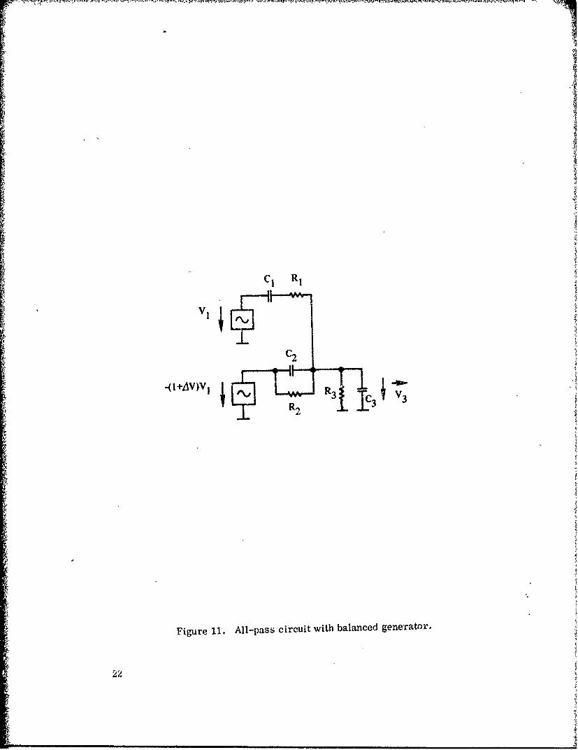
4. RC REALIZATION WITH BALANCED GENERATOR
One of the implementations of the all-pass filter suggested by Dome is anRC network fod by two out-of-phase signals, figure 11. In view of the worst-case analysis, performed later, a possible difference of the magnitdes of theinput voltagc ] has been considered. The frequency response of the transferf,'nct.on is,
V3 (1+.aW)C
) - +av C1I 1 C2 + 3
L ( +'xv)Ra 1 R 2 C + " r1 2C'C,,>
4. 1 Il-as..' Conditions
T"he all-pass conditions of tbe circuit of figure 11 are derived for 'aV = 0.TIhe general all-pass transfer function (2) may be written as
O 2 2W 7 0 0 0
1l 0w,) + 2cj + a2 2(1
Compared to (30), it follows that (31) describes an all-pass if
2 1 1 1 1 2azR: + + .I + #..L 1.._
C2 +C RIC 1 RIC+C R1 C2 - R1C1 - R2 C2
V 2 2 1
21 22 + a +(31)
I- O) ew
C RI
C2
Figure 11. Al-pas5 circuit with balanced generator.
22
-(I+AV)
I R3 vC 3
R?
aind
it RC)
2 3RCI~CO+C R 11C
1 ~ 3 i1,' 2l 12
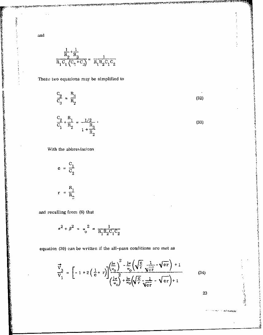
Theso two equations may be simplified to
2 13C2 R 13
:
C R (32)3 2
C RS 1/ (33)
C 1 RR 12 -
With the abbreviations
C 1
C2
R,
Rn-'
and recalling from (6) that
a2 +,?2 2 1
RIR 2 CIC 2
equation (30) can be written if the all-pass conditions are met as
v = +r - -/.Vr (34
23(LI JrC i
[- 1 2(-!+r (34
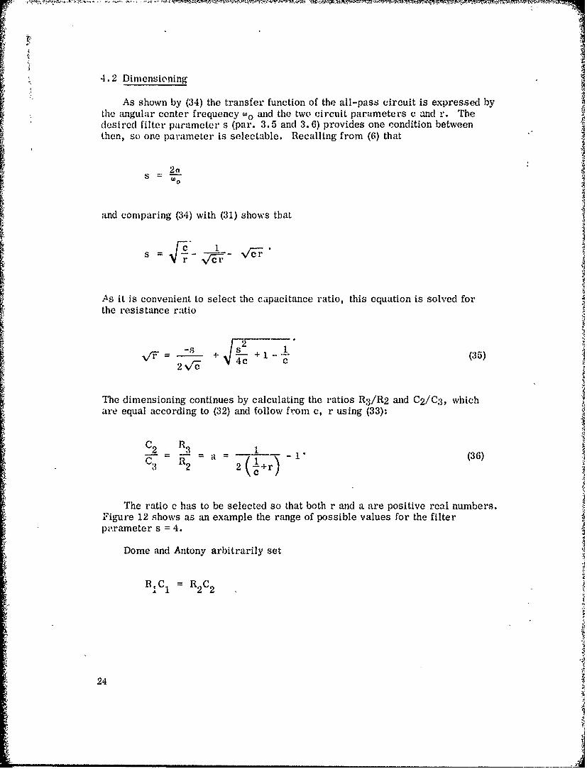
4.2 Dimensioning
As shown by (34) the transfer function of the all-pass circuit is expressed bythe angular center frequency wo and the two circuit parameters c and r. Thedesired filter parameter s (par. 3.5 and 3.6) provides one condition betweenthen, so one parameter is selectable. Recalling from (6) that
2a
and comparing (34) with (31) shows that
As it is convenient to select the capacitance ratio, this equation is solved forthe resistance ratio
s2 1
-s9 + (35)2v'~ 4c
The dimensioning continues by calculating the ratios R 3 /R2 and C2 /C 3 , whichare equal according to (32) and follow from c, r using (33):
C2 3 (36)
C R3 2 - 2 -+r
The ratio c has to be selected so that both r and a are positive real numbers.Figure 12 shows as an example the range of possible values for the filterparameter s = 4.
Dome and Antony arbitrarily set
RCI = R2C224 2
24

15
a5
I 1 I 1 I0 5 10 15
C.. C
Figure 12. Possible circuit parameters for s ; 4.
25

wbich mcnies
i
and
c s +2
a
After a set of circuit parameters c, r, a has been found, continue by
selecting one of the three
resistors or capacitors
R " Ra c 0 aR R 2 R3 1 -<--- - - 3
then obtain
ci 1 (37)C1 o R- 1 w ooCI
c C a C R RCI-- 2 - - 30 3 R1~ R2--- R3
4.3 Effect of Component Tolerances
With
nominal parameters ao a. c,,.r;
nominal componen'ts R R R Co C Co, V 0;Lis 2o' 3o' C1 0 2o' :3o'
actual components P,, R2, R3 , Cl, C2 , C31, AV;
26

the transfer function of one all-pass section (31) can be written as:
V I.- (+jA _E 1 +E 23 '2 =(38)
VC +C (i 2 E1 2 3 W +J E +E
where
E R10 20 C10 1 C201 f R R C N,- C1 2 R C 2 2
10 -R210 C-0 C20E2 R R C C1 2 1 2
R20 1 R30 R10R aR 11C C1 1+
E = C; RI el0 __2 +1 C3 R1 C1 / r
2 C3
20 a 30 20 30
R10 (20 +1 300
R I I aR 31 2 1 _ 3
10 a20 C
Equation (38) contains only the nominal circuit parameters and ratios of nomi-nal to actual component values. In this way, the effert of percent',e variationsof components on the frequency response can be studied for ,.Fiore generalnetwork. A compkter program, listed in appendix 1, has been written to calcu-l' e the worst-cise phase difference for combination of specified componenttoleranccq.
Tolerances may be specified for each of the three resistors, for each ofthe three capacitors and for the symmetry of the input voltages. The programas,umes the same tolerances for corresponding elements in the two channels.It furth r uses the fact thnt the tolerance of ; pair of components (e.g., 112 inchanne' I and 2) affects the response most if the two components are at
22

opposite ends of their tolerance range (channel 1: R2 = R20 + _R2;channel 2: R2 = R20 - 4R 2 ). The program goes through all possible combina-tions of tolerances (27 combinations if all tolerances arespecified as non-zero);and in each case sweeps through the frequency range and notes the phase c.iffer-ences at the extramra and the band edges. The smallest and largest values forall combinations at each of these points is printed out.
The band edges are specified as the ratio f2 /fl, from which the filteiparameters s,b, 8 are immediately computed (eq. 23, 24, 25). The running
ffrequency variable is x = ff and it is swept from
in
- 1- f to X 2 ' ;
The frequency variable actually substituted into equation (38) is (using (12)and (13)):
For Channel 1 For Channel 2
_ f b 1;o1 2 fm b
Since the absolute frequency limits need not be specified, the worst-caseanalysis is valid for any filter of such configuration characterized by band widthf2/ii and implementtion parameters c(chan. 1), c(chan. 2).
4.4 Amplifier Considerations
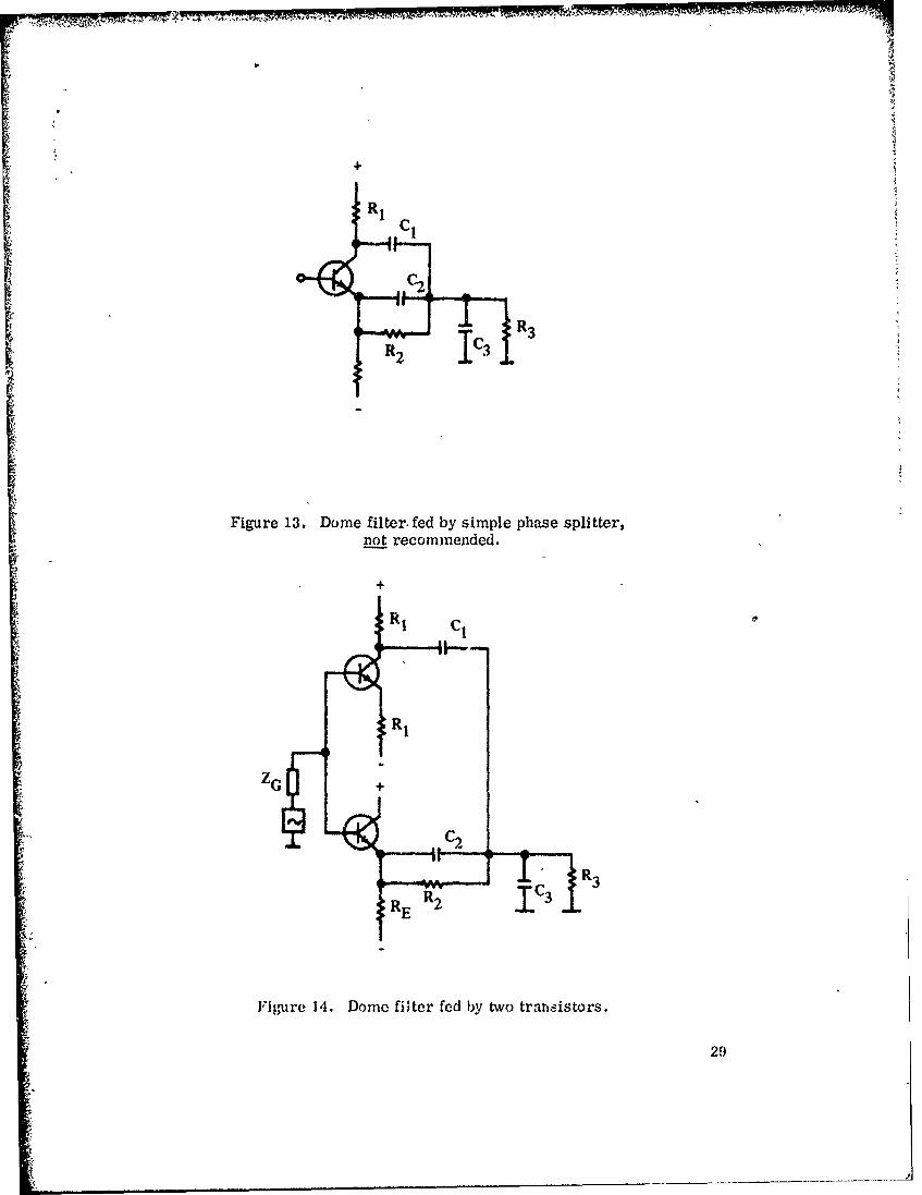
The Dome filter implementation treated in thi ' chapter must be fed by twosignals of eoual amplitude and opposite phase (fig. 11). A simple one--tram,--torphase splitter as in figure 13 probably does not suffice when a phase error of afew degrees is desired. * The change of the emitter load C2 I R2 with frequencyreflects onto the equivalent collector voltage source.
This interaction is considerably reduced in the two-transistor circuit offigure 14. It should work satisfactorily when the emitter load impedances R1and RE II R2 II C2 , multiplied by the transistor current gain, each are largecompared to the generator impedance Z .
*supported by experience relayed by K. Sann, IIDL
28
C
C2
Figure 13. Dome filter, fed by simple phase splitter,not recommended.
+
RI l
ZG +
R 2
RE R2 3
Figure 14. Dome fiiter fed by two transistors.
29

Impedance relationships need not be considered when feeding the Dome filterby a pair of integrated-circuit operational amplifiers (fig. 15). One operationalamplifier works in the inverting mode, the other in the noninverting mode.With unity gain, as shown, the voltage symmetry depends upon the two resis-
AIRFtors R F being equal. With , resistor tolerance -- , the gain tolerance is
R F
AV = 2 - - •'~~F
The amplifiers may provide voltage gain; in that case there are two pairs ofresistors whose ratio must be equal.
A phase difference between the outputs of the inverting and noninvertingamplifier is possible, particulariy at frequencies approaching the upper limit ofthe operational amplifier; this error is not included in the worst-case analysis.
4.5 Example
Design a phase difference network of 90 degrees with a maximum nominaldeviation of :E2 degrees and a bandwidth as great as possible, extending, ifpos, ible, from 600 to 10000 Hz.
8 20
RF
+ C2
Figure 15. Dome filoler fed by two operational amplifiers.

, According to the scheme of figure 9:
s 3. 868144
b = 2. 050514
z = -1.260048
Using the desired edge frequencies to find a suitable center frequency
f V 600"1O00Hz ; 2449.5 t1zm
f 2450 Hz.m
The actual band limits are then
f, = 610.9 H1z
f2 9826 IN
and the other characteristic frequencies are
f 01 1194.82 Hz
f fo2 5023.76 iz
1 971. i Hz
fmax2 6180 Iz
rn "x2

It is generally advantageous to select capacitor, rather than resistorvalues, to be standard values. * For each all-pass section, two capacitorscan be selected. In this example, C1 and C2 were chosen by trial and error sothat C3 comes close to a standard value too. Depending on the permissibleactual phase error, this standard value may be usable. If nothing else, itmakes breadboarding easier.
Section 1 Section 2
C1 :-- 12nF C = 6.8nFC2 - 2.2nF C2 1 ni'
c = 5.454545 c = 6.800000
r = 0.158105 r = 0.196085
a = 0.464393 a 0.457115
C3 4.737nF C3 2.188nF33
R1 10.31 k a R = 5.380 kB
1 2 = 65.20kQ R 2 - 27. 44 kfl2 2
R,, - 30.28ki R= 12.54 k Q
The results of the worst-case analysis are shown in table I. After listingof the parameters, the frequency is swept once with the nominal values to ensurethat the input data are correct. The next seven resultis show the effect of thevariation of one component at a time. As it is, R1 and C2 affect the phase dif-ference mainly at the higher frequencies, R 2 and C1 mainly at the lower frequen-cies. A voltage unbalance shows up, although to a lesser degree, at both endsof the band. The effect of variations of 113 and C3 is only about one-fourth of thatof the other resistors and capacitors.
With one percent tolerance of all components (except one-half percent forR F if the circuit shown in figure 15 is used), the possible phase error is almostthree degree, in addition to the nominal two degree error with ideal compon-ents. If all resistor tolerances arce reduced to one-fourth percent, the possibleerror is close to four degrees, or twice the nominal arror. If standard values
"(±1 percent) are ordered for C,3, its possible variation may be up to 1.7 percentfrom the theoretical value; as the last output shows, the error is increased onlyvery slightly.
*Although one-pcr'cent capacitors way be ordered with any arbitrary nominal value,nonstandard values have higher prices and longer delivery time. This was foundto be the case with ceramic capacitors from Aerovox, Erie and Vitramon.
32

TABLE I. l)OME CIRCUIT WITH BALANCED GENERATOR
NOMINAL tANDWIOTH F2/FI= 16.0800NOM. DERIVEG PARAN. Sz3.867941 8*2.050461 DELTA=2.00
NON. REALIZ. CHAN.1 A= 0.46434 C= 5.45450 R= 0.15811CHAN.2 0.45706 6.80000 0.19610
Fl I.MAX MIN 2.4AX F2
OP NOM./DEG 88.00 92.00 88.00 92.00 88.00
COMPONENT VARIATION 1./-PCT) RI R2 R3 Cl C2 C3 Dv( O P P O S I T E I N C H A N .I , 2 ) .........
1.00 -0.00 -0.00 -0.00 -0.00 -0.00 -0.00
0P MAX /DEG 88.14 92.26 88.64 92.93 88.9bOP MIN /DEG 87.86 V.74 87.35 91.06 87.04
COMPONENT VARIATION (+/-PCT) RI R2 R3 CI C2 C3 DV(OPPOSITE IN CHAN* 1tZ) --- - -- -- -- - - -- - - -- - - -- - - -
-0.00 1.00 -0.00 -0.00 -0.00 -0.00 -0.00
OP MAX /DEG 88.71 92.68 88.43 92.11 88.nzOP MIN /DEG 87.29 91.32 87,57 91.89 87.)8
COMPONENT VARIATION (+/-PCT) RI R2 R3 Cl C2 C3 OV(OPPOSITE IN CHAN.1,2)
-0.00 -0.00 1.00 -0 00 -0.00 -0.00 -0.CO
DP MAX /DEG 83.25 92.25 88 .fL 92.15 88.12OP.MIN /DEG 87.75 91.74 87.79 91.85 87.88
COMPONENT VARIATION (+I-VCT) Rl R2 R3 Cl C2 C3 OV(OPPOSITE IN CHAN.l,2) --
-0.00 -C.00 -0.00 1.00 -0.00 -0.00 -0.00
OP MAX /OEG 88.96 92,93 88.65 92.26 8814DP MIN /DEG 87.04 91.06 d7.35 91.74 87.86
COMPONENT VARIATION (+/-PCT) RI R2 R3 C1 C2 C3 ;V(OPPOSITE IN CHAN.1,2 ----------------------
-0.00 -0.00 -0.00 -0.00 1.00 -0.00 -O.CO
DP MAX /CEG 88.02 92.12 88.43 92.67 88.70DP MIN /OEG 87.98 91.88 87.57 91.32 87.30
COMPONENT VARIATION (+/-PCT) RI R2 R3 CI C2 C3 OV(OPPOSITE IN CHAN.1,2)
-0.00 -0.00 -0.00 -0.00 -0.00 1.00 -0.00
DP MAX /OEG 88.12 92.14 88.21 92.26 88.26OP MIN /OEG 87.88 91.85 87.79 91.74 87.74
COMPONENT VARIATION (+/-PCT) R! R2 R3 Cl C2 C3 OV(OPPOSITE IN CHAN.lj2)- ------------------------------------------
-0.00 -0.00 -0.00 -0.00 -3.00 -0.00 1.00
OP MAX /DEG 88.62 92.51 87.99 92.51 A8.62OP MIN /DEG 87.37 91.48 87.99 91.48 87.37

TABLE I. DOME CIRCCIT WITH BALANCED GENERATOR (Continued)
COMPONENT VAOIATION (+/-PCT) RI RZ R3 CI C2 C3 Ov(OPPOSITE IN CI*.N.192.................
1.00 1.00 1.00 1.00 1.00 1.00 1.00
OP MAX /DEG 90.80 94.89 90.58 94.89 90.80OP MIN /DEG 85.15 89.07 85.41 89.07 85.15
COMPONENT VARIATION (+/-PCT) RI R2 R3 Cl C2 C3 oV(OPPOSITE IN CHAN192) -
0.25 0.25 L.00 1.00 1.00 1.0 0.50
OP MAX /OEG 89.87 93.94 89.78 93.86 89.T7OP MIN /OEG 86.11 90.05 86.22 9G.13 86.21
COMPONENT VARIATION (+/-PCT) RI R2 R3 Cl C2 C3 BV(OPPOSITE IN CHAN.I,2)
0.25 0.7= 1.00 1.00 1.00 1.70 0.50
OP MA-X /OEG 89.95 94.0 89.9, 94*.04 89.95OP PIN /DEG 86.03 89.95 86.07 C1.95 86.03
3
I.
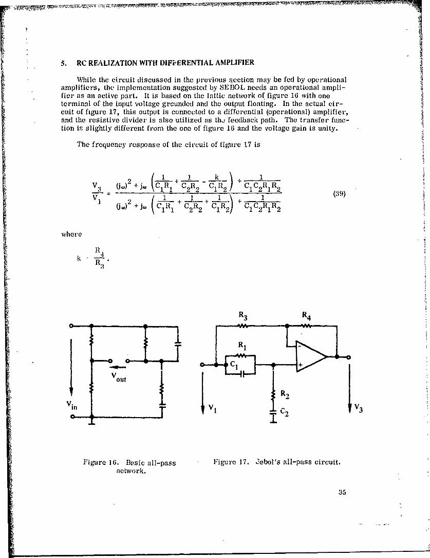
5. RC REALIZATION WITH DIFi'ERENTIAL AMIPLIFIER
While the circuit discussed in thc previous section may be fed by operationalamplifiers, the implementation suggested by SEBOL needs an operational ampli-fier as an active part. It is based on the lattic network of figure 16 with oneterminal of the input voltage grounded and the output floating. In the actual cir-cult of figure 17, this output is connected to a differential (operational) amplifier,and the resistive divider is also utilized as th,! feedback path. The transfer func-tion is slightly different from the one of figure 16 and the voltage gain is unity.
The frequency response of the circuit of fig-e 17 is
( 1 j - +V1 j) +o C 1 R1 C 2 R2 C1R /t C IC 2f RR2
1(39)V ~ + L + 1CR
a.) ++ CR CR C 2RR\11 2 2 1 2/ 1 2 1 2
4
R3 Rh3 R4
Vi V1 %V 3
RI
ou!
in0- V1 [1V3
Figure 16. B,,sic all-pass Figure 17. .3ebol's all-pass circuit.network.
35

5.1 All-pass Condition
Comparing equation (39) with the general all-pass transfer function (31) showsthat the constant terms of numerator and denominator arc always identical, and,comparing with (16)
10o .IC2R 1 R2
The other condition for an all-pass function is then
-I i k - 1 i1 1-1I{ + _+ + ___ _ -C R C R C R C R C R C R1 1 2 2 1 2 1 1 2 2 1 2
or with the abbreviations
Cl
C
the all-pass condition is
9k - . 2c -' 1. (40)
If it is met, the transfer function may be written as
V-1 ,_ :SL(41)
3(;

~5.92 Dimensioning
dI
The desired filter parameter s provides again one relation between thecircuit parameters c and r, so one of them is selectable. Comparing (41) with(31) and (16) shows that
S - V"V + ;
$
this is solved for r to seleelt
s c (42)V 2 (0+1) (L 21 -
Figure 18 shows the possible range of c, r, k in a typical case.
100
30
10 - e k
3
0.3
0.1C
0.03
0.01 I _ I 10.2 0.5 1 2 5
-. .C
Figure 18. Solutions of r,k vs c for s = 4.Solid curves are for the + sign in equation (42).
37

This all-pass realization contains only two capacitors, both of which can beselected. Furthermore, they may be the same. These are two attractive featuresof this circuit.
After C1, C2 and thus c have been selected, r and k are found from equa-tions (42) and (40);
R!R2 -o[C1C--r'
2~ 1
and R1 follows from r. The absolute values of R3, R4 do not enter; their ratiois given by k. The impedance level should be between the operational amplifierinput and output impedances.
5.3 Effect of Component Tolerances
A worst-case analysis has been worked ouc similar to the one described insection 4.3. The computer program is listed in appendix 2. The analysisconsiders variations of the passive components only, not imperfections of theoperational amplifier. As the latter is involved very tightly in the performanceof the circuit, and finite gain, input impedance or common mode rejection cer-tainly show an effect, the analysis is not as useful as in the other case. It showsnecessary tolerances for the passive, components; however, keeping these toler-.ances does not in itself guarantee the desired performance.
5.4 Example
Requirements and filter parameters as in section 4.5. For each channel,both capacitors are selected, and selected equal. For r, the + sign in equa--tion (42) is used, because it results in a lower impedance spread.
Section 1 Section 2
c Cc:
C1 C2 10nF C C2 2.2nF
r =2.646158 2.646158
k 3.755813 k 3.755813
i2 t 8.85kvi
It 21. 7kfl it 1 23.4 kf0
It 5.6 kf R. 5.6 kfl3
R 21.0 kf Q l 21.0 kfo
38

The result of the worst-case analysis is shown in table 1I. R1 and C2affect the phase difference mostly at lower frequencies, 1R2 and C 1 mostly athigher frequencies. Deviations of R:3 and R4 have a lesser, effect at both endsof the band, none in the center. A tolerance of one percent of all passive com-
ponents results in a worst-case error of almost 3.5 degrees in addition to thenominal error of two degrees. Resistor tolerances of 0. 25 percent approxi-mately halve the excess error.
The last result of table I shows that somewhat different circuit parametersgive about the same tolerance sensitivity.
The sensitivity of this implementation is also about the same as the onetreated in section 4.
6. SUMMARY
This report describes a simple method of determining the parameter andcomponent values and tolerances for a cla,'s of 90 degree phase differencenetworks. After a short discussion of previously published papers on this sub-ject and the limitations of their theoretical treatment, the transfer function onsecond order all-pass networks, the parameters of two such networks providinga 90-degree phase difference between their output signals, and the relationshipsof these parameters to the phase ripple and bandwidth are derived. Simple andstraightforward computational methods, requiring only a desk calculator, fordetermining the filter parameters based on either the required bandwidth oe thepermissible phase deviation are then outlined.
Two different inductorless networks for the implementation of the all-passfunction and their respective advantages and disadvantages are described, andequations defining component values are derived. Here, as with the filterparamecers above, the flexibility and options available to the designer arestressed. For each circuit, a computer program is listed and discussed whiclkperipits the ca!culation of the worst effect of component tolerances on the phasedifference. Transistor and integrated-circuit amplifiers suitable for the activeparts of the circuits are considered briefly. Computational methods are illus-trated by examples where the filter parameters, the circuit components, andworst-case phase errors for both implementations are calculated.
39
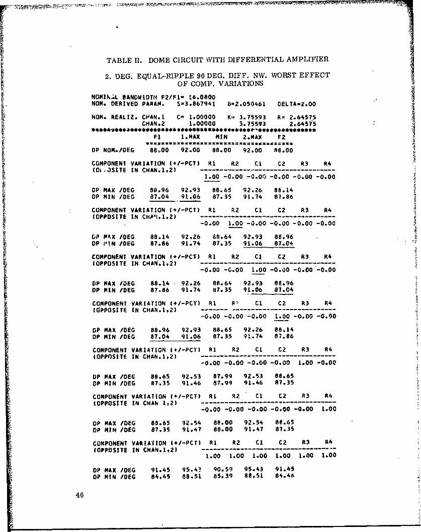
r]
TABLE II. DOME CIRCUIT WITH DIFFERENTIAL AMPLIFIER
2. DEG. EQUAL-RIPPLE 90 DEG. DIFF. NW. WORST EFFECTOF COMP. VARIATIONS
NOMIN.L SANDWIOTH F2/Fl- 16.0800NON. DERIVED PARAN. Sx3.867941 8=2.050461 OELTA-2.0O
NON. REALIZ. CFAN.1 Cz 1.00000 K- 3.75593 R= 2.64575CHANs2 1.00000 3.75593 2.64575
Fl l.MAX MIN 2.MAX F2
OP NOM./OEG 88000 92.00 88.00 92.00 88.00
COMPONENT VARIATION (+/-PCT) R1 R2 Cl Cz R3 R4(0ir3SITE IN CHAN.192)
1.00 -0.00 -0.00 -0.00 -0.00 -0.00
OP MAX /DEG 8a,96 92.93 88.65 92.26 88.14DP MIN /DEG 87,04 91.06 87.35 91.74 87.86
COMPONENT VARIATION (+/-PCT) RI R2 Cl C2 R3 R4(OPPOSITE IN CH4.1--2)------------------------
-0.00 1.00 -0.00 -0.00 -0.00 -0.00
GP MAX /OEG 88.14 92.26 68.64 92.93 88.96OP PIN /DEG 87.86 91.74 87.35 91.06 87.0'
COMPONENT VARIATION (+/-PCT) RI R2 Cl C2 R3 R4(OPPOSITE IN CHAN.I,2)- ----------------------------
-0.00 -C.00 1.00 -0.00 -0.00 -0.00
OP MAX /DEG 88.14 92.26 88.64 92.93 88.96
DP MIN /DEG 87-86 91.74 87.35 91.06 87.04
COMPONENT VARIATION (+/-PCT) RI R, Cl C2 R3 R4(OPPOSITE IN CHAN.1,2) -0.00 -0.00 -0.00 1.00 -0.00 -0.00
DP MAX /EG 88.96 92.93 88.65 92.26 8-.14OP MIN /DEG 87.04 91.06 87.35 91.74 87.86
COMPONENT VARIATION (+/-PCY) RI R2 Cl C2 R3 R4(OPPSTE IN CHAN.1,2)- --------------------------
-0.00 -0.00 -0.00 -0.00 1.00 -0.00
OP MAX /DEG 88.65 92.53 87.99 92.53 88.65OP MIN /DEG 87.35 91.46 17.99 91.46 87.35
COMPONENT VARIATION ( /-PCT) RI R2 Cl C2 R3 R4(OPPOSITE IN CHAN 1,2)------------------------
-0.00 -0.00 -0.00 -0.00 -0.00 1.00
OP MAX /DEG 88.65 92.54 88.00 92.54 88.65
OP MIN /DEG 87.35 91o47 88.00 91.47 87.35
COMPONENT VARIATION (./-PCT) RI R2 Cl C2 R3 R4
(OPPOSITE IN CHAN.*E2) ""1.00 1.00 1.00 1.00 1.00 1.00
OP MAX /DEG 91.45 95.4! 90.59 95.43 91.45OP NIN /OEG 84.45 88,51 85.39 88.51 84.46
40

TABLE II. DOME CIRCUIT WITH DIFFERENTIAL AMPLIF!.b (Continued)
COMPONENT VARIATION ( /-PCT) RI R2 C1 CZ R3 R410PPOSITE IN CMAN.192)-- - - - - - - - - - - - - - - - -0.25 0.25 L.00 1o00 0.25 0.25
OP MAX /DEG 89.69 93.76 89.62 93.76 39.69DP MIN /OEG 86.2 90.23 86.39 90.23 86.29
NON. REALIZ. CtAN.1 C= 0.50000 K- 3.15261 Ra 1.73519C"AN.2 0.50000 3.15261 1.73519
Fl 1.MAX MIN 2.MAX F2
OP NO./CEG 88.00 92.00 d8.00 92.00 88.00
COMPONENT VARIAtION (./-PCT) RI R2 Cl C2 R3 R4IOPPOSITE ;N C"AN.1,Z) .......
O A9 .1.00 ).0 O0.0 1.00 1.00 1.00OP NAX /DEG 91 40 95.39 90.59 95.39 91.41UP MIN /DEG 8'.51 86.55 85.39 88.55 84.51
*1I

LITERATURE CITED
1. Dome, R. B., "Wideband Phase Shift Networks," Electronics, Vol 4,Dec 1946, p 112
2. Antony, R.T., "Dome Filter Design and Analysis Programs,"HDL-TM-70-26, 1970
3. Sebol, R., "Design of Active 90-Degree Phase Difference Networks,HDL-TM-68-18
4. Bedrosian, S.D., "Normialized Design of 90-Degree Phase DifferenceNetworks," fRE Trans. on Circuit Theory, June 1960
5. See, for instance, L. Weinberg, Network of Analysis and Synthesis,McGraw Hill, 1962, p 285
Preceding page blank 43

APPENDIX I
COMPLiTER PROGRAM FOR THE WORST--CASE ANALYSIS OF THE DOME FILTERCIRCUIT WITH BALANCED GENERATOR.
INPUT DATA:
Data J Format Comment
f2/f FI0.6
c(chin. 1), c(chan. 2) 2F10.6
-AR11 .R, AR 3 , - C , AC AC AV 7][5.2 Relative deviations in percent(tolerance set)
......... .Any number of tolerance sets
blank I If analysis for different
c(chan. 1), c(chan.2) circuit parameters is
. desired *
. . . .Any number of tolerance
setsJ
-'As many sets of data cards may be used as desired.
Preceding page blank 45

PROGRAM LISTING
IPE45)EQUIVALENCE ( IA(1),Il),t IA(Z),12),( IA(3),13),(IA(4)914)1
P1=3.1415926RE*D(591) F
I FORMAT(2f10.6)91-SQRT( 1./F)XZ=SQRT(F)GuI (XI+KC2)**2-4. )/(XI+X2-2.1S-SQRT(G*SvRNTVG*G.2.*G*SQkT( 2.*G-4.)))B=SQRT(1.+S*S/2.-G+SQRT((1.4S*S/2ZG)**2-1Id)DELTAZ2.*ATAN(4 S*S-2.*S*(B-1 ./B3-(8-l./B)**2)/tS*S+2.*S(B-.I
WRITE(6v2)FSv8,DELTA2 FORI4AT(IIHI 2.DEG.EQUAL-RIPPLE 9ODEG.DJFF.NW. WORST EFFECT OF
ICOMP.VARIATIONS/25HONONINAL BANDWIDTH F2/Flu*F8.4/ZSH NON. DERIVEDr2 PARAN. SzeFS.6,5P BaPF8.699P DELTAtF4.2)
3 EAO(5.1), C00 4 Izl92I, R(I~at-S,2./SQRT(C(I))+SQRT(S*S/4./CII)4L.-I./CIIJ))**2I WRITE(6t5) (A( I) C(I) ,RU), 1,I2)
5 FORMAT(25HONOM. REALIZ. CHAN.i A=,F8.5t5H CxvF8.5,5H RavF8.51/14X,6HCHAN.2,3F13.5/1X,584 11*)DO 6 Na1,8
6 DIN)u0.GO TO 12
* 7 ftEA045,8):(O(N),N=lt7)8 FORKAT(7F5*2)
IF(D( 1) .80.0..AND.D( 2) *EQ.O. .AND.Of 3i.EQ.O. .AND.O( 4) kg. .AND.10(5),oEQ.0..ANO.0(6).EQ.O..AND.(7.Ek'.G.) GO TO 300 10 14195PEFPIl1.
10 PEI(l)=PI12 00 13 Naly7
IA(N)%l13 IFIDINP.E0.) AAIN)=2
DO 50 NtaltJ1
Y(I*2J*I. 0(1)1100.*(-1.)**NXDO 50 N?n1,I2Y(2v1)1.9OV(2)/I00.*f1. )**KZ
Y(3*2)sJ.-0(3)/I00.*i-1.)**N3
D0 50 tal14
Y(4#2)u1,.Q(4)ILOO.*(-1. 3**N4
DO 5:' N51l,15
DO 50 P48.1916
46

-T1PROGRAM LISTING (Continued)
I DO 50 N7uli?
Y(79Z)al.-0(7?I100.*(-1. )**N700 15 1414
1/Y$1.1)/Y(',,I)-SQRT(R(I)*C( 1) /Yt2,I)/Y( 5,I)E4ZI)1l./YtlIJIY(291)/Yf4,1)/Y(5,l3
I/A(l)) 1./SORT(R( )*C(1) )/YI 1,L /Vt ',1 )4SQRT(C(I)/R(1) )/Y( 1,11/2 (Yf5I14'Y(6#I)/At1))
15 Et4,1)stl./Y12,I)+1./Y(3,I3/AII))/Y(l1. 1/Y(4.II/(V(5.1)4Yt6.1)/IAt I))NalDo 30 14101O1lF(N.EQ.J..ANO.I.LT.1OA) GO TO 30XmX1*(X2/X1)**(FLOATl 1-1)1100.)[ ~ ~~a-ARC'(-X*B*E( 1, 13.( 2, 1)-C X* ) **2 j.ARCT( X*B*E(3,1) , 491)-C X*B)1**234ARCTC-X/B*E(1,2),E(2,2)-(X/B)**2)-ARCT(X/8*E(3,2),E(4,2)-2(X/B)**2)
20 1-i) 20920,2120 PE(1)-P
GO 70 3021 IF(P-PO) 26,3092222 IFIN-2) 23,24,25
r-23 PE1Z)aPGO TO 30
24 N03
GO T0 30
21 IFIN-2) 27,28,2917 PNu2
GO 10 3028 PEf3loP
GO TO 3029 Nu430 POOP
PE15loPf?0 35Iq.IF1PE(I).GT*PE~fl()) PEP(I)wPE(I)
35 IF(PE(I)*LT.PENC 13) PENt 1)xPEfJ)50 CONTINUE
IF(D18)) 51,51,6051 00 52 1*19552 pECI)wPEII)/PI*180.
WRITEt6v55) PE*55 FORMAYC17X,2HFl.5X,5H1.NAX,4X,3HNN4X,5N2.MAX,4X,2HF2/
115Xt38(IH*)/I3H DP NON./OEG 95F8.2)D(8121.GO TO?7
60 00 62 lil#5PEP(1)=PHPt I)/PI*I80.
62 PECI)=PaI()/PI*lao.WRITE46965) (D(N)*Nx1,?)tPEPPEM
*65 FORMAT(69HOCOMPONENT VARIATION (*/-PCT) RI R2 R3 CI c;12 C3 DV/2314 IOPPOSITE IN CHAN.192)*6Xv42(lH-)/2$X,7F6.23/13HODP MAX /DEG t5FO%2/13g OP MIN /DEG #SFO.21Gao TO 7'No
47

APPENDIX 2
COMPUTER PROGRAM FOR THE WORST-CASE ANALYSIS OF THE DOME FILTER
CIRCUIT WITH OPERATIONAL AMPLIFIER
INPUT DATA:
Data Format Comment -
f2fl F0. 6
c(chan. 1), c(chan. 2) 2F10.6
AR1, AR2' AC1' AC 2 , AR 3, AR 4 16F5.2 Tolerance in percent(tolerance set)
. . . . . . . . !Any number of tolerance sets
blank If analysis for different
c(chan.1), c(chan.2) circuit parameters is
desired *
Any number of tolerancesets
*As many sets of data cards may be used as desired.
49Preceding page blank
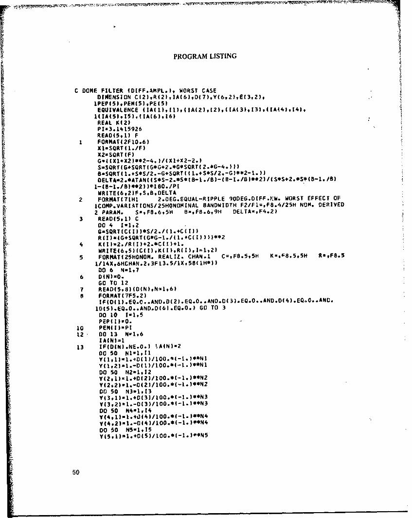
PROGRAM LISTING
C COME FILTER (DIFF.AMPL.19 WORST CASE
D1I4ENSION C(2),R(2),JA(6),D(7),Y(6,2,EI 3,2),1PEPf5),PEM(5) ,PE(5)EQUIVALENCE (IAE )1),1),(!A(2)912),(IA(3).13),(1A44)914)t
REAL K(2)PIx3. 1415926REAO(591) F
I FORMAT(2FI0.6)Xl- SQRT(1./F)X2*SQRT(F)GUIXI+X2)**2-4. )/IXI+X2-2.)SaSQfT(G,QRT(G*G+2.*G*SgRT(2.*G-4.)))BuSQRftl.S*S/2.-G+SgRT(41.+S*S/2.-G)**2-1.))DELTAs2.*ATAN((S*S-2.*S*t8-l./8)-(8-l./B)**2)/(S*S+2.*S*(B-l./B)
WRITE(692)FtS,B*DELTA2 FORMAY(71N1 2.OEG.EQUAL-RIPPLE 9CDEG.DIFF*KW. WORST EFFECT OF
ICOMP.VARIATIONS/25HONOMINAL BANDWIDTH F2/Fl=9F8.4/25H NOM. DERIVED2 PARAM. SaFB.695H BuF8.6t9H DELTA2,F4.2)
3 READ(5,1) CDO 4 11.#2
4 K(I)=29/R(I)+2.*C(I)41.WRITE(6,5) (C(I) ,K( 1) R( I), 1- 12)
5 FORKAT(Z5HONOM. REALIZ. CHAN-1 C=9F8.595H K3[,r8.5,5H Ra,F8.51/14X,6HCHAN.2,3FI3.5/1X,58(IH*))00 6 N-197
6 D(NI-O.Go To 12
? READ(598)1O(N),N21961a FORMAT(7F5.Z)
IF( DI ).*EQ.0. .AND.D( 2). EQ.0. *AND.D( 3). EQ.0. .AND.D(4) .EQ.0. .ANC.ID(5).EQ.0.*AND.D(6)*EQ.O.) GO TO 300 10 1-1,5PEPt I)SO.
10 PENII)"PI12 - DO 13 N-1,6
IA (NI =l13 IF(D(N).NE.O.) 'A(N)x2
00 50 NIz,.I1Y(1,1)-l.40(I/100.*(-1. I**NIY4192)al.-D( I)/100.*(I- **00 50 N2=1012Y(2,1)xi.,D(2)/100.*(-l. )**N2Y(2*21.1.-0(23/100.*(I. )**N2DO 50 N3*1913Y(3*1)wl.+O(3)/100.*('1. )**N3
Y(3t2)xl.4O(3)I100.*It1. I*N4
00 50 N~ultI5
Yi5,1)zlo+0(5)I100.*(I. )**N5
50

PROGRAM LISTING (Continued)
DO 50 N6-1,16
Y(6v1)-l.o(6)/jO.* .)**N6DO 15 1*1,2Gal./Ytl.J)/Y(3,1)/SQRT4C(I,.R(fI
15 E(3,I)2uG+HSQRT(R(I)/CI I))/(9)Y3N=Z00 30 1*1#101IF(N.EQ.4.ANO*..1lo) GO TO leD
G*E(2#1)-(X*B)**2
Pu-ARCT(X*8.E(I l)eG)+ARCT(X*a*E(3,1ttG)+ARCT(X/B*E(!9)z )lARCT(X/8*Ef3t2!,H)
IF(1 11'P20,2092120 PEIkP
GO TO .O2L IF(P-P01 26,30,2222 IF(N-21 23,24.2523 PE(2)*P
GO TO 3024 Nac3
GO TO 3025 PE(4)uP
GO TO 3026 IF(N-2) 27#28.29
GO TO 3028 PE(3)mP
29 *
PE(5 i-P
35 IF(Pktl)4LT*PEMII)) PEMII)UPEtI)5o CONTIN4UE
MFOM)j 51,51t6051 00 52 1*1,552 PE(I)xPE(1)PIp*180.
WRZ1E(69551 PE55 FORMATI l?Xt2HFI,5X,5HlMAX4X3HMN,4Xt5H2MAXf
4X 2HF2,115Xq38UlHwp,13kl OP NOM./DEG t5F8.2)
GO TO 76C 00 62 1*195
PEF(IIZPEP( l1/PI*ia0.62 PEpfI)=PEN(1/PIsp*180.
WRITEf6t65u0D(N) ,NmI,6),pPEPPEN65 FORMAT(63HOCOMPONENT VARIATION (+/-PCT) Al R2 cI C2 R13 R4/23H (OPPOSITE IN CHANo1,2)v6Xv35flp.-)/28X 6 2/213HOOP MAX /DEG v5F8*2/13H DP MIN /DEG S5FB.Z)
GO TO 7E NO
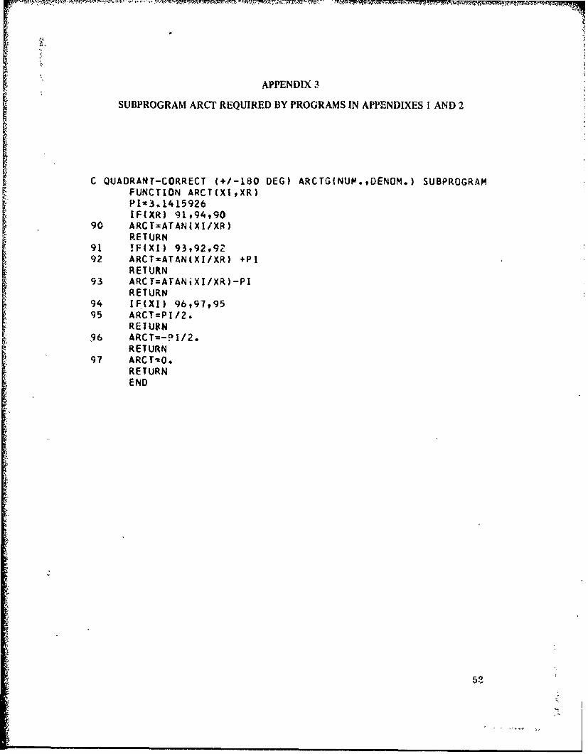
APPENDIX 3
SUBPROGRAM ARCT REQUIRED BY PROGRAMS IN APPENDIXES I AND 2
C QUADRANT-CORRECT (+/-180 DEG) ARCTG(NUP.tDENOM.) SUBPROGRAMFUNCTION ARCT(XIXR)PI-3*1415926IF(XR) 91,94,90
90 ARCT=ATANIXI/XR)RETURN
91 !F(XI) 93,9920292 ARCT-ATAN(XI/XR) +Pl
RETURN93 ARCT=ATANiXI/XR)-PI
RETURN94 IF(XI) 9697,9595 ARCT=PI/2.
REIURN96 ARCT=-PI/2.
RETURN97 ARCT'O.
RETURNEND
54