Embed Size (px)
Citation preview
Distributed Amplifiers
Ali Medi
Outline
• Introduction
• DA principles of operation
• DA with artificial T-lines
• DAs with improved gain stages
• Noise in DAs
• DAs with tapered T-lines
• Loss compensation in DAs
• Transformer-based DA
2
Introduction
• Distributed amplifier basic idea first introduced in
1936 [Percival 36] to overcome traditional GBW
limit of vacuum tube amplifiers.
• The name distributed amplifier first introduced in
[Ginzton 48].
• The key idea is to absorb parasitic capacitances of
the transistors into T-lines to improve the amplifier
bandwidth.
3
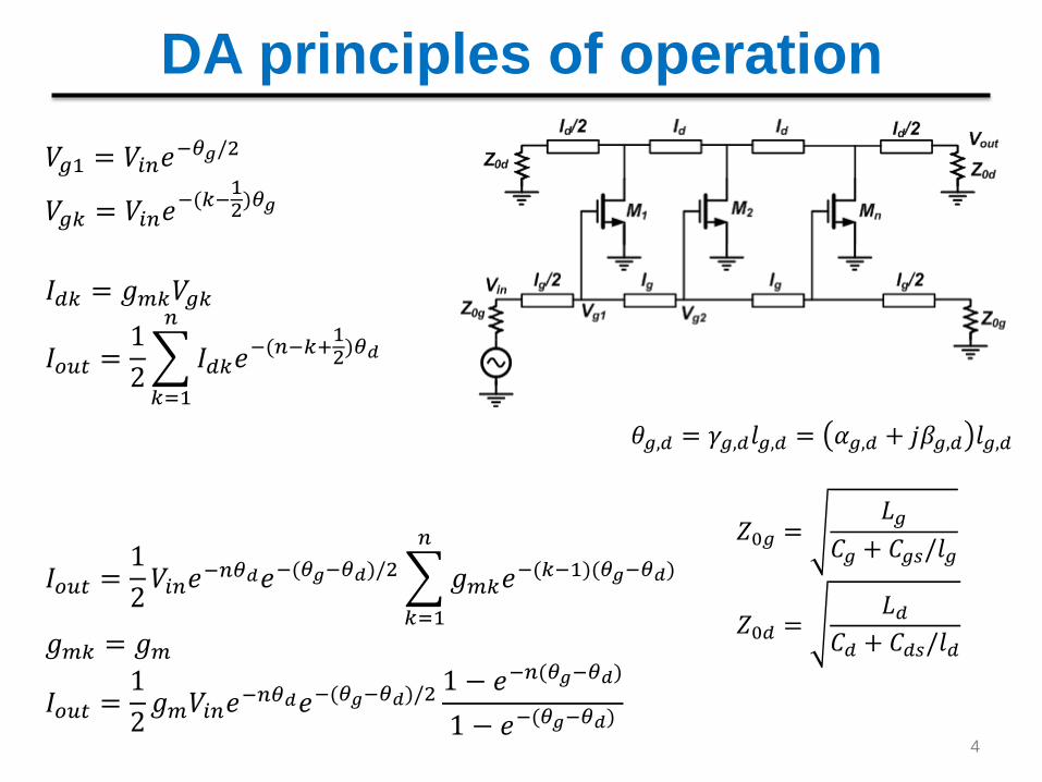
DA principles of operation
𝑉𝑔1 = 𝑉𝑖𝑛𝑒−𝜃𝑔/2
𝑉𝑔𝑘 = 𝑉𝑖𝑛𝑒−(𝑘−12)𝜃𝑔
𝐼𝑑𝑘 = 𝑔𝑚𝑘𝑉𝑔𝑘
𝐼𝑜𝑢𝑡 =1
2 𝐼𝑑𝑘𝑒
−(𝑛−𝑘+12)𝜃𝑑
𝑛
𝑘=1
𝐼𝑜𝑢𝑡 =1
2𝑉𝑖𝑛𝑒−𝑛𝜃𝑑𝑒−(𝜃𝑔−𝜃𝑑)/2 𝑔𝑚𝑘𝑒
−(𝑘−1)(𝜃𝑔−𝜃𝑑)
𝑛
𝑘=1
𝑔𝑚𝑘 = 𝑔𝑚
𝐼𝑜𝑢𝑡 =1
2𝑔𝑚𝑉𝑖𝑛𝑒
−𝑛𝜃𝑑𝑒−(𝜃𝑔−𝜃𝑑)/21 − 𝑒−𝑛(𝜃𝑔−𝜃𝑑)
1 − 𝑒−(𝜃𝑔−𝜃𝑑)
4
𝑍0𝑔 =𝐿𝑔
𝐶𝑔 + 𝐶𝑔𝑠/𝑙𝑔
𝑍0𝑑 =𝐿𝑑
𝐶𝑑 + 𝐶𝑑𝑠/𝑙𝑑
𝜃𝑔,𝑑 = 𝛾𝑔,𝑑𝑙𝑔,𝑑 = 𝛼𝑔,𝑑 + 𝑗𝛽𝑔,𝑑 𝑙𝑔,𝑑
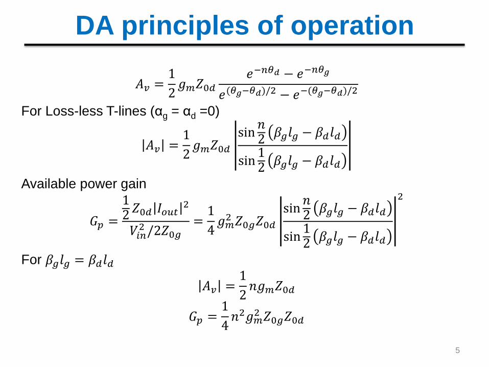
DA principles of operation
𝐴𝑣 =1
2𝑔𝑚𝑍0𝑑
𝑒−𝑛𝜃𝑑 − 𝑒−𝑛𝜃𝑔
𝑒(𝜃𝑔−𝜃𝑑)/2 − 𝑒−(𝜃𝑔−𝜃𝑑)/2
For Loss-less T-lines (αg = αd =0)
𝐴𝑣 =1
2𝑔𝑚𝑍0𝑑
sin𝑛2𝛽𝑔𝑙𝑔 − 𝛽𝑑𝑙𝑑
sin12𝛽𝑔𝑙𝑔 − 𝛽𝑑𝑙𝑑
Available power gain
𝐺𝑝 =
12𝑍0𝑑 𝐼𝑜𝑢𝑡
2
𝑉𝑖𝑛2 /2𝑍0𝑔
=1
4𝑔𝑚2 𝑍0𝑔𝑍0𝑑
sin𝑛2𝛽𝑔𝑙𝑔 − 𝛽𝑑𝑙𝑑
sin12𝛽𝑔𝑙𝑔 − 𝛽𝑑𝑙𝑑
2
For 𝛽𝑔𝑙𝑔 = 𝛽𝑑𝑙𝑑
𝐴𝑣 =1
2𝑛𝑔𝑚𝑍0𝑑
𝐺𝑝 =1
4𝑛2𝑔𝑚2 𝑍0𝑔𝑍0𝑑
5
DA principles of operation
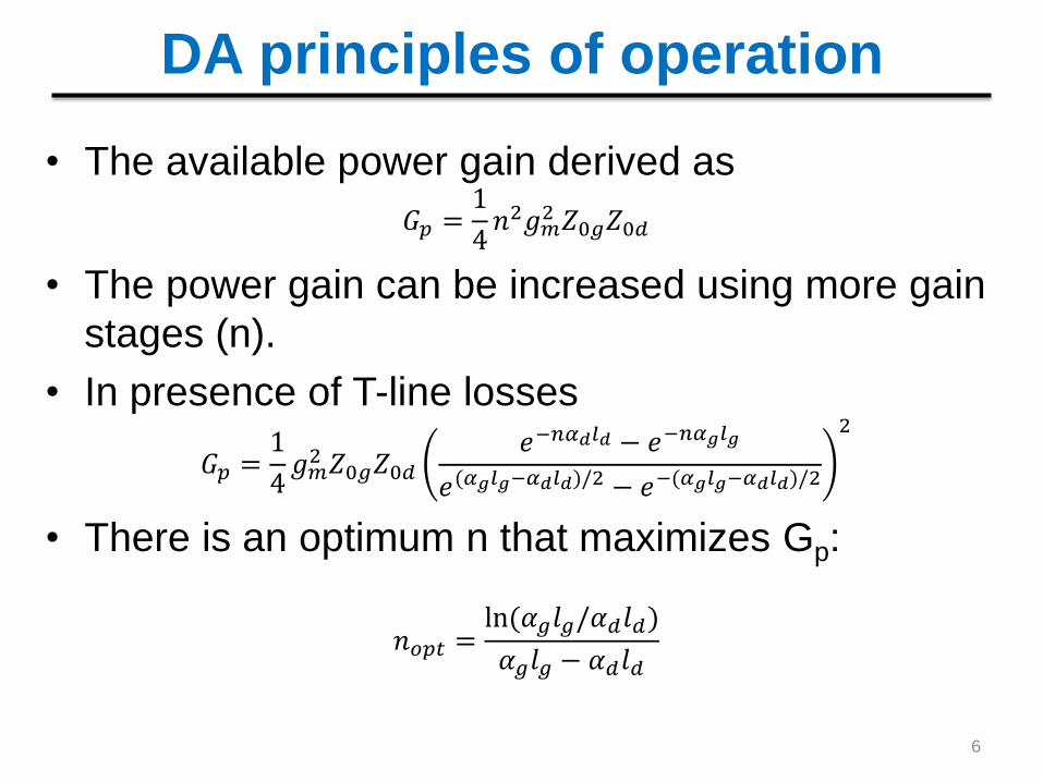
• The available power gain derived as
𝐺𝑝 =1
4𝑛2𝑔𝑚2 𝑍0𝑔𝑍0𝑑
• The power gain can be increased using more gain
stages (n).
• In presence of T-line losses
𝐺𝑝 =1
4𝑔𝑚2 𝑍0𝑔𝑍0𝑑
𝑒−𝑛𝛼𝑑𝑙𝑑 − 𝑒−𝑛𝛼𝑔𝑙𝑔
𝑒(𝛼𝑔𝑙𝑔−𝛼𝑑𝑙𝑑)/2 − 𝑒−(𝛼𝑔𝑙𝑔−𝛼𝑑𝑙𝑑)/2
2
• There is an optimum n that maximizes Gp:
𝑛𝑜𝑝𝑡 =ln(𝛼𝑔𝑙𝑔/𝛼𝑑𝑙𝑑)
𝛼𝑔𝑙𝑔 − 𝛼𝑑𝑙𝑑
6
DA principles of operation
• It is desired to have T-lines with high Z0.
• Narrow T-line: higher loss (ohmic and skin effect),
electron-migration limit (~ 1mA/um2).
• Line losses are frequency-dependent; affecting
gain flatness.
7
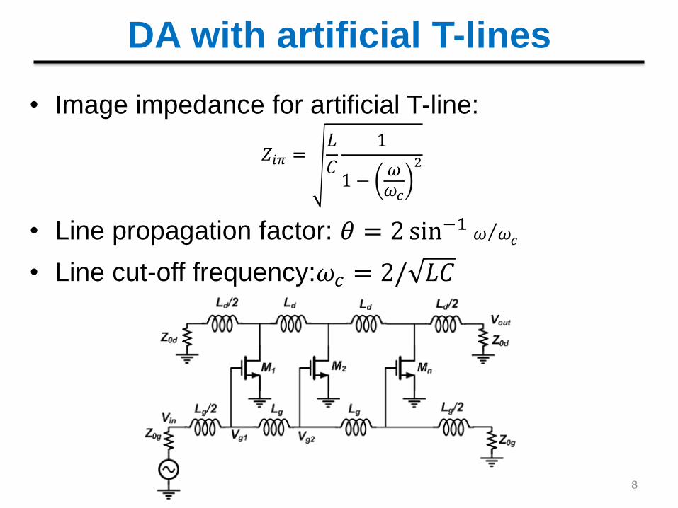
DA with artificial T-lines
• Image impedance for artificial T-line:
𝑍𝑖𝜋 =𝐿
𝐶
1
1 −𝜔𝜔𝑐
2
• Line propagation factor: 𝜃 = 2 sin−1 𝜔 𝜔𝑐
• Line cut-off frequency:𝜔𝑐 = 2/ 𝐿𝐶
8
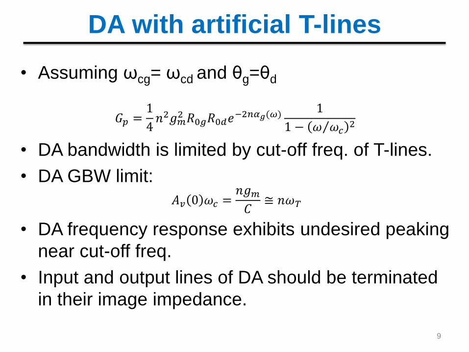
DA with artificial T-lines
• Assuming ωcg= ωcd and θg=θd
𝐺𝑝 =1
4𝑛2𝑔𝑚2 𝑅0𝑔𝑅0𝑑𝑒
−2𝑛𝛼𝑔(𝜔)1
1 − 𝜔 𝜔𝑐 2
• DA bandwidth is limited by cut-off freq. of T-lines.
• DA GBW limit: 𝐴𝑣 0 𝜔𝑐 =
𝑛𝑔𝑚𝐶≅ 𝑛𝜔𝑇
• DA frequency response exhibits undesired peaking
near cut-off freq.
• Input and output lines of DA should be terminated
in their image impedance.
9
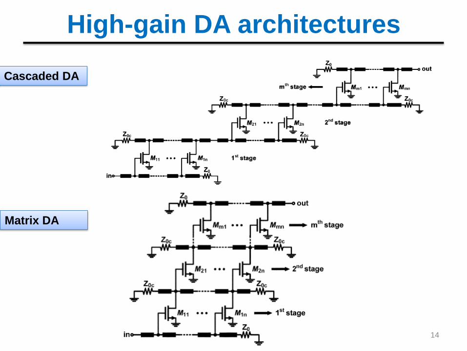
High-gain DA architectures
14
Cascaded DA
Matrix DA
DA with improved gain stage
Design issues in DA gain stages:
• High Gm value is desired to enhance DA gain.
• Gm variations with freq. affect the DA gain flatness.
• BW of DA is limited by BW of Gm stages.
• Noise contribution of Gm stage should be low.
• The DA stability is compromised when using multi-
stage amplifiers as gain stage.
15
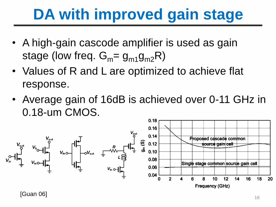
DA with improved gain stage
• A high-gain cascode amplifier is used as gain
stage (low freq. Gm= gm1gm2R)
• Values of R and L are optimized to achieve flat
response.
• Average gain of 16dB is achieved over 0-11 GHz in
0.18-um CMOS.
16 [Guan 06]
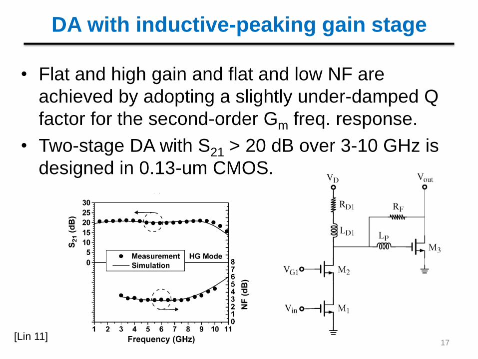
DA with inductive-peaking gain stage
• Flat and high gain and flat and low NF are
achieved by adopting a slightly under-damped Q
factor for the second-order Gm freq. response.
• Two-stage DA with S21 > 20 dB over 3-10 GHz is
designed in 0.13-um CMOS.
17 [Lin 11]
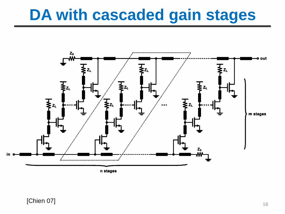
DA with cascaded gain stages
18 [Chien 07]
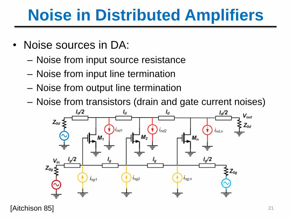
Noise in Distributed Amplifiers
• Noise sources in DA:
– Noise from input source resistance
– Noise from input line termination
– Noise from output line termination
– Noise from transistors (drain and gate current noises)
21 [Aitchison 85]
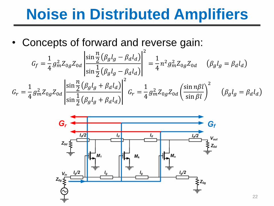
Noise in Distributed Amplifiers
• Concepts of forward and reverse gain:
𝐺𝑓 =1
4𝑔𝑚2 𝑍0𝑔𝑍0𝑑
sin𝑛2 𝛽𝑔𝑙𝑔 − 𝛽𝑑𝑙𝑑
sin12 𝛽𝑔𝑙𝑔 − 𝛽𝑑𝑙𝑑
2
=1
4𝑛2𝑔𝑚2 𝑍0𝑔𝑍0𝑑 𝛽𝑔𝑙𝑔 = 𝛽𝑑𝑙𝑑
𝐺𝑟 =1
4𝑔𝑚2 𝑍0𝑔𝑍0𝑑
sin𝑛2 𝛽𝑔𝑙𝑔 + 𝛽𝑑𝑙𝑑
sin12 𝛽𝑔𝑙𝑔 + 𝛽𝑑𝑙𝑑
2
𝐺𝑟 =1
4𝑔𝑚2 𝑍0𝑔𝑍0𝑑
sin 𝑛𝛽𝑙
sin 𝛽𝑙
2
𝛽𝑔𝑙𝑔 = 𝛽𝑑𝑙𝑑
22
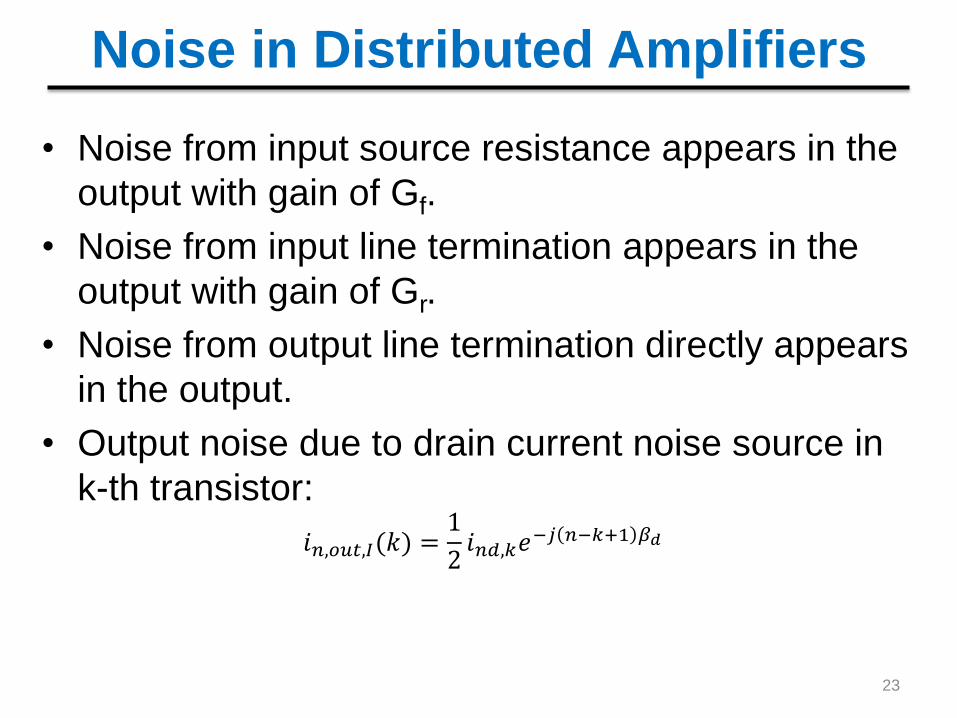
Noise in Distributed Amplifiers
• Noise from input source resistance appears in the
output with gain of Gf.
• Noise from input line termination appears in the
output with gain of Gr.
• Noise from output line termination directly appears
in the output.
• Output noise due to drain current noise source in
k-th transistor:
𝑖𝑛,𝑜𝑢𝑡,𝐼(𝑘) =1
2𝑖𝑛𝑑,𝑘𝑒
−𝑗 𝑛−𝑘+1 𝛽𝑑
23
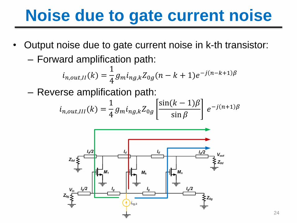
Noise due to gate current noise
• Output noise due to gate current noise in k-th transistor:
– Forward amplification path:
𝑖𝑛,𝑜𝑢𝑡,𝐼𝐼(𝑘) =1
4𝑔𝑚𝑖𝑛𝑔,𝑘𝑍0𝑔(𝑛 − 𝑘 + 1)𝑒
−𝑗 𝑛−𝑘+1 𝛽
– Reverse amplification path:
𝑖𝑛,𝑜𝑢𝑡,𝐼𝐼𝐼(𝑘) =1
4𝑔𝑚𝑖𝑛𝑔,𝑘𝑍0𝑔
sin(𝑘 − 1)𝛽
sin𝛽𝑒−𝑗 𝑛+1 𝛽
24
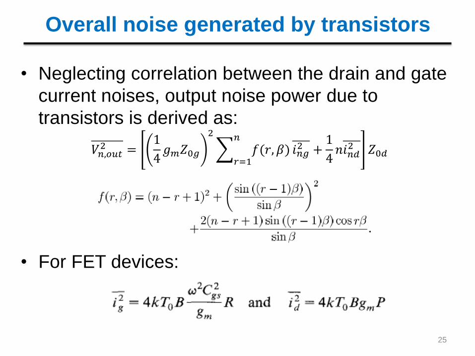
Overall noise generated by transistors
• Neglecting correlation between the drain and gate
current noises, output noise power due to
transistors is derived as:
𝑉𝑛,𝑜𝑢𝑡2 =
1
4𝑔𝑚𝑍0𝑔
2
𝑓(𝑟, 𝛽)𝑛
𝑟=1𝑖𝑛𝑔2 +1
4𝑛𝑖𝑛𝑑2 𝑍0𝑑
• For FET devices:
25
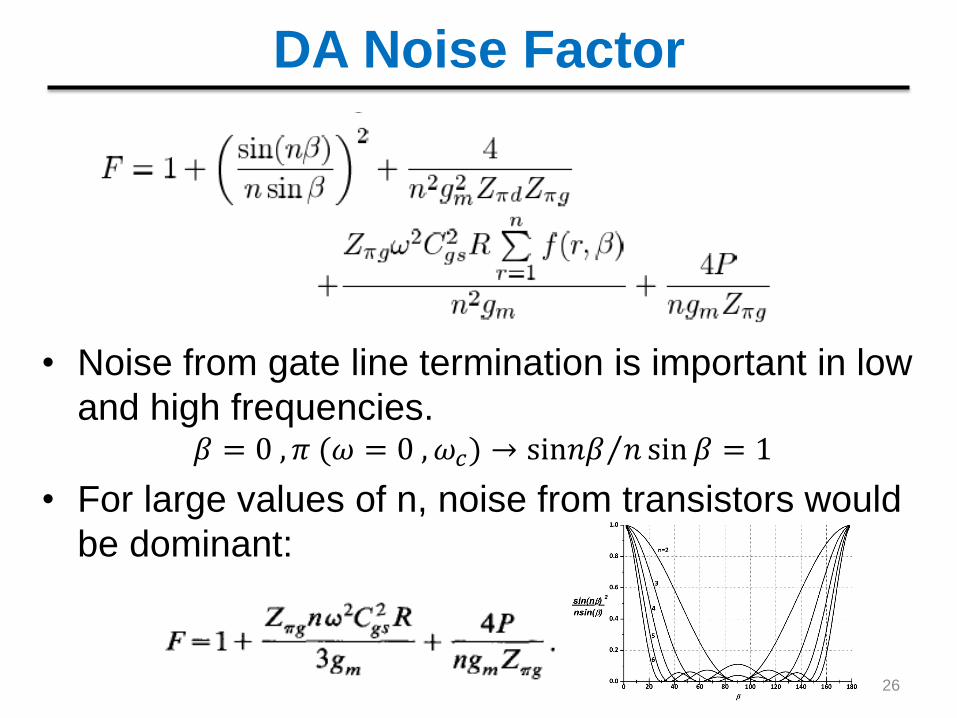
DA Noise Factor
• Noise from gate line termination is important in low
and high frequencies. 𝛽 = 0, 𝜋(𝜔 = 0, 𝜔𝑐) → sin𝑛𝛽 𝑛 sin 𝛽 = 1
• For large values of n, noise from transistors would
be dominant:
26
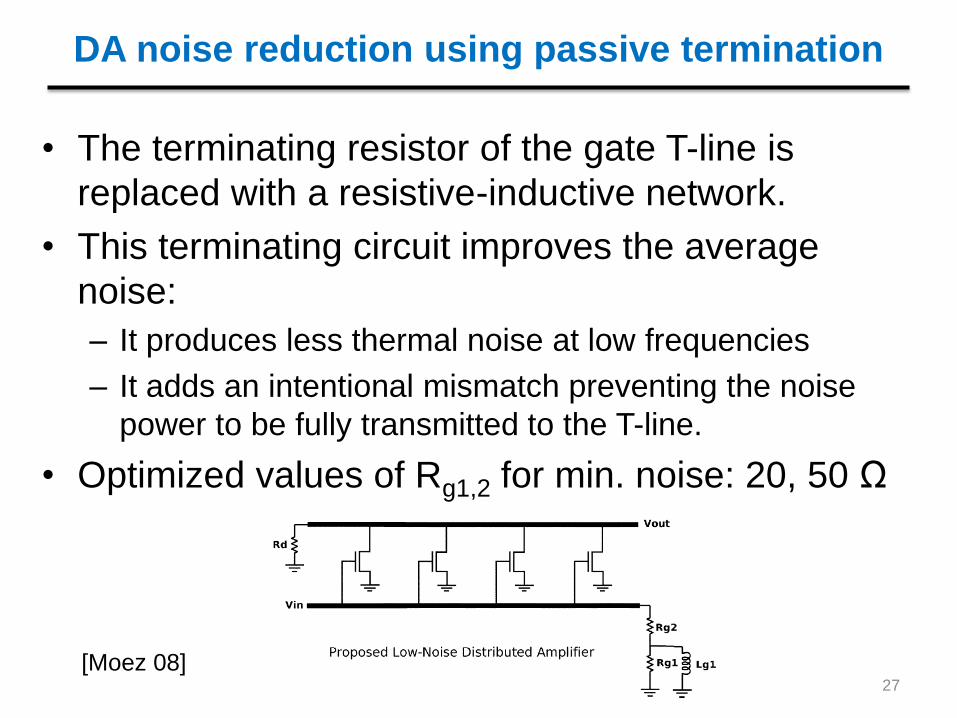
DA noise reduction using passive termination
• The terminating resistor of the gate T-line is
replaced with a resistive-inductive network.
• This terminating circuit improves the average
noise:
– It produces less thermal noise at low frequencies
– It adds an intentional mismatch preventing the noise
power to be fully transmitted to the T-line.
• Optimized values of Rg1,2 for min. noise: 20, 50 Ω
27
[Moez 08]
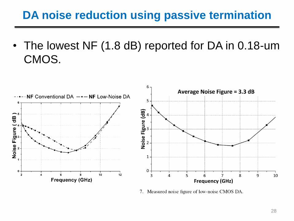
DA noise reduction using passive termination
• The lowest NF (1.8 dB) reported for DA in 0.18-um
CMOS.
28
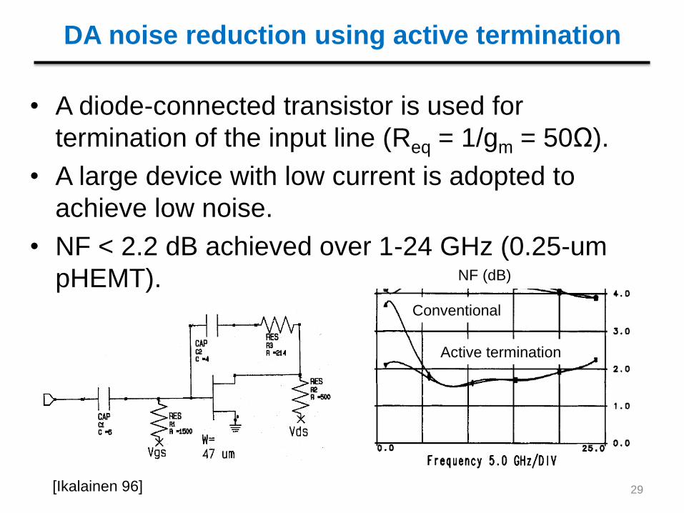
DA noise reduction using active termination
• A diode-connected transistor is used for
termination of the input line (Req = 1/gm = 50Ω).
• A large device with low current is adopted to
achieve low noise.
• NF < 2.2 dB achieved over 1-24 GHz (0.25-um
pHEMT).
29 [Ikalainen 96]
Conventional
Active termination
NF (dB)
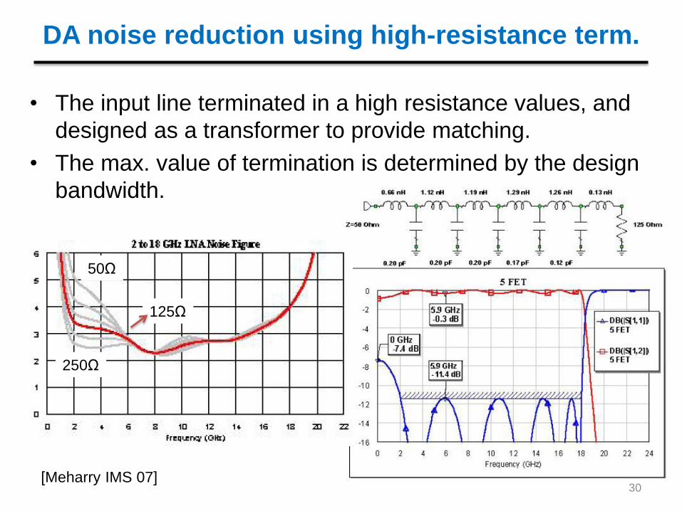
DA noise reduction using high-resistance term.
• The input line terminated in a high resistance values, and
designed as a transformer to provide matching.
• The max. value of termination is determined by the design
bandwidth.
30 [Meharry IMS 07]
50Ω
125Ω
250Ω
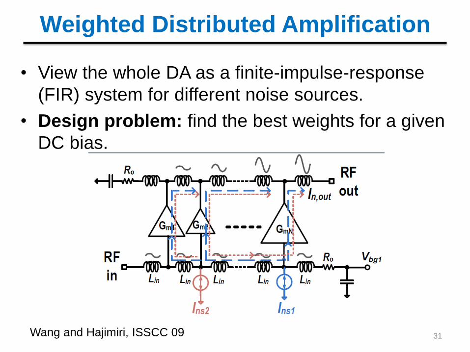
Weighted Distributed Amplification
• View the whole DA as a finite-impulse-response
(FIR) system for different noise sources.
• Design problem: find the best weights for a given
DC bias.
31 Wang and Hajimiri, ISSCC 09
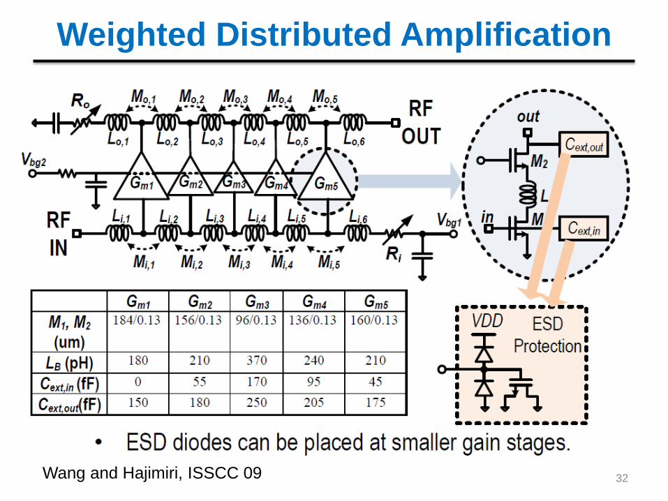
Weighted Distributed Amplification
32 Wang and Hajimiri, ISSCC 09
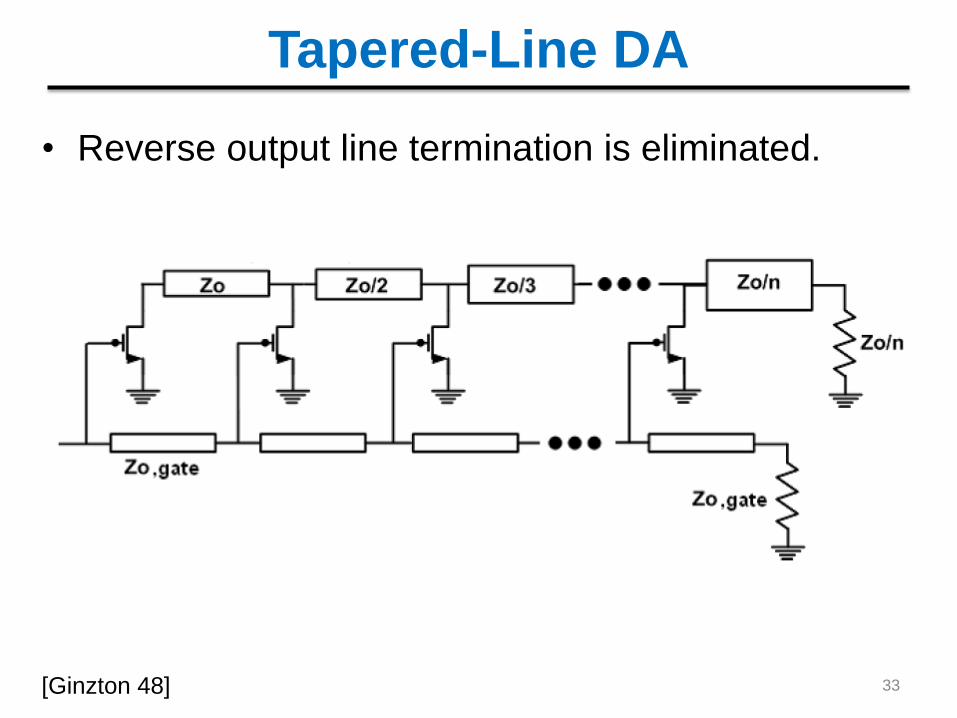
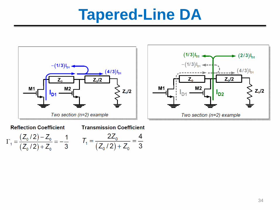
Tapered-Line DA
• Reverse output line termination is eliminated.
33 [Ginzton 48]
Tapered-Line DA
34
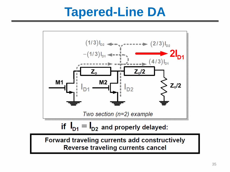
Tapered-Line DA
35
Tapered-Line DA design issues
• Condition ID1 = ID2 cannot be satisfied perfectly;
leading to reflection in output line.
• If Z0/n is different with load termination, a
transformer would be needed at the output.
• For large values of n, very narrow or wide lines
would be required in the output line sections.
36
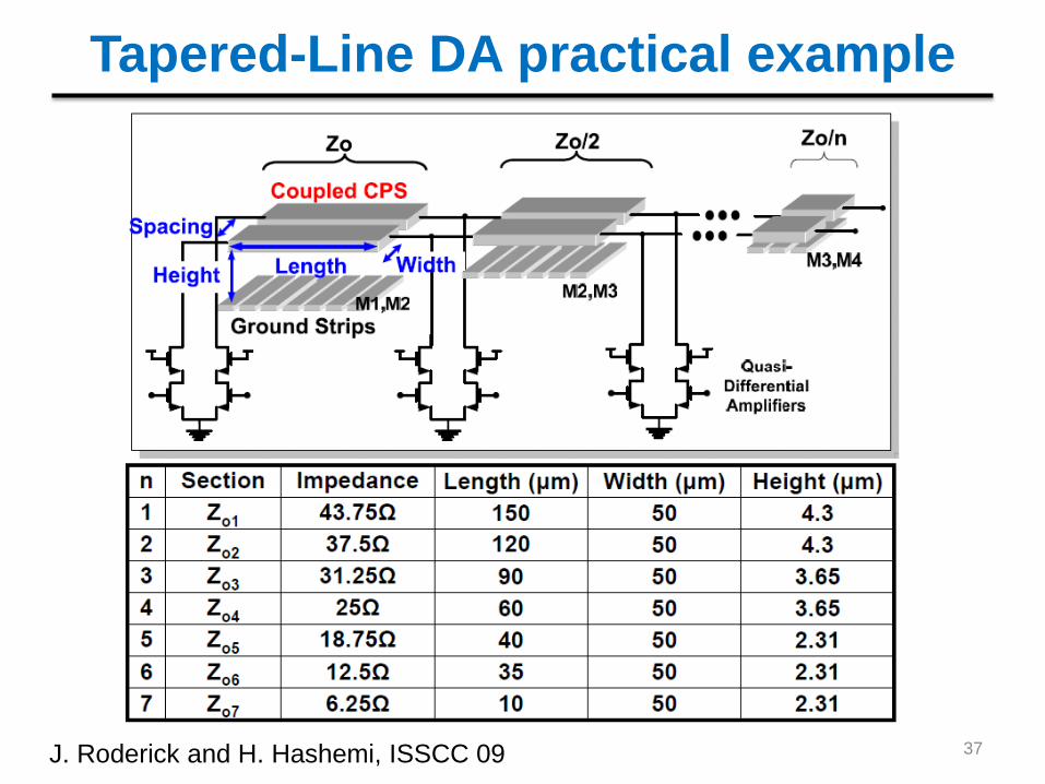
Tapered-Line DA practical example
37 J. Roderick and H. Hashemi, ISSCC 09
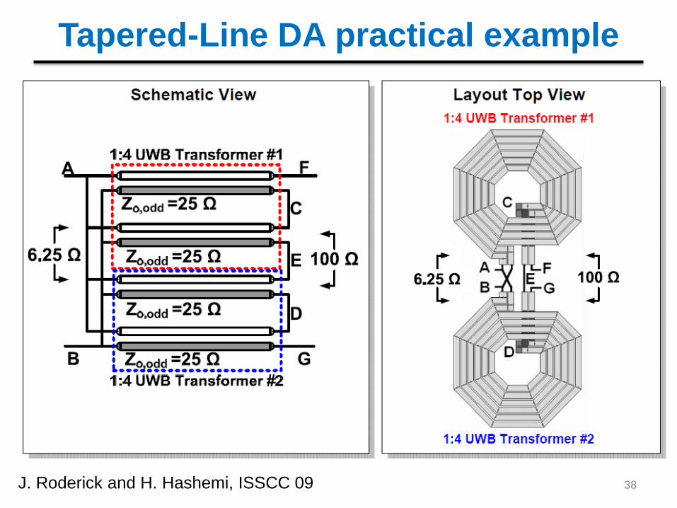
Tapered-Line DA practical example
38 J. Roderick and H. Hashemi, ISSCC 09
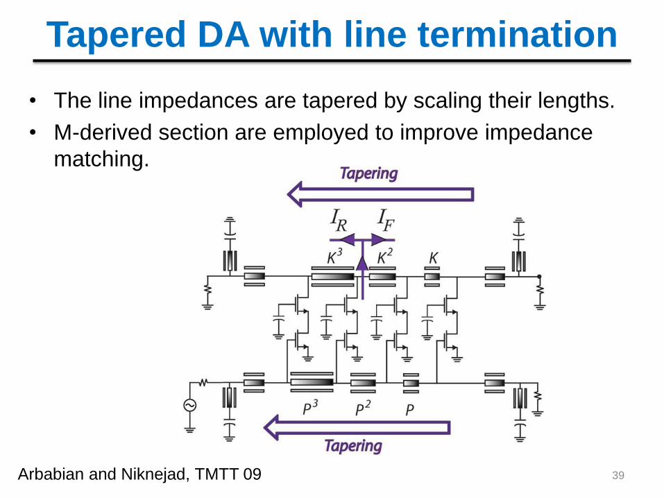
Tapered DA with line termination
• The line impedances are tapered by scaling their lengths.
• M-derived section are employed to improve impedance
matching.
39 Arbabian and Niknejad, TMTT 09
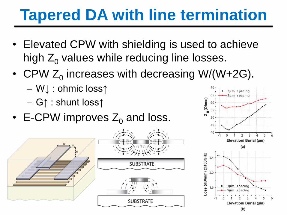
Tapered DA with line termination
• Elevated CPW with shielding is used to achieve
high Z0 values while reducing line losses.
• CPW Z0 increases with decreasing W/(W+2G).
– W↓ : ohmic loss↑
– G↑ : shunt loss↑
• E-CPW improves Z0 and loss.
40
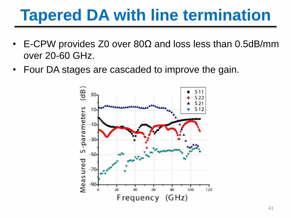
Tapered DA with line termination
• E-CPW provides Z0 over 80Ω and loss less than 0.5dB/mm
over 20-60 GHz.
• Four DA stages are cascaded to improve the gain.
41
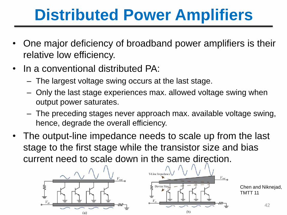
Distributed Power Amplifiers
• One major deficiency of broadband power amplifiers is their
relative low efficiency.
• In a conventional distributed PA:
– The largest voltage swing occurs at the last stage.
– Only the last stage experiences max. allowed voltage swing when
output power saturates.
– The preceding stages never approach max. available voltage swing,
hence, degrade the overall efficiency.
• The output-line impedance needs to scale up from the last
stage to the first stage while the transistor size and bias
current need to scale down in the same direction.
42
Chen and Niknejad,
TMTT 11
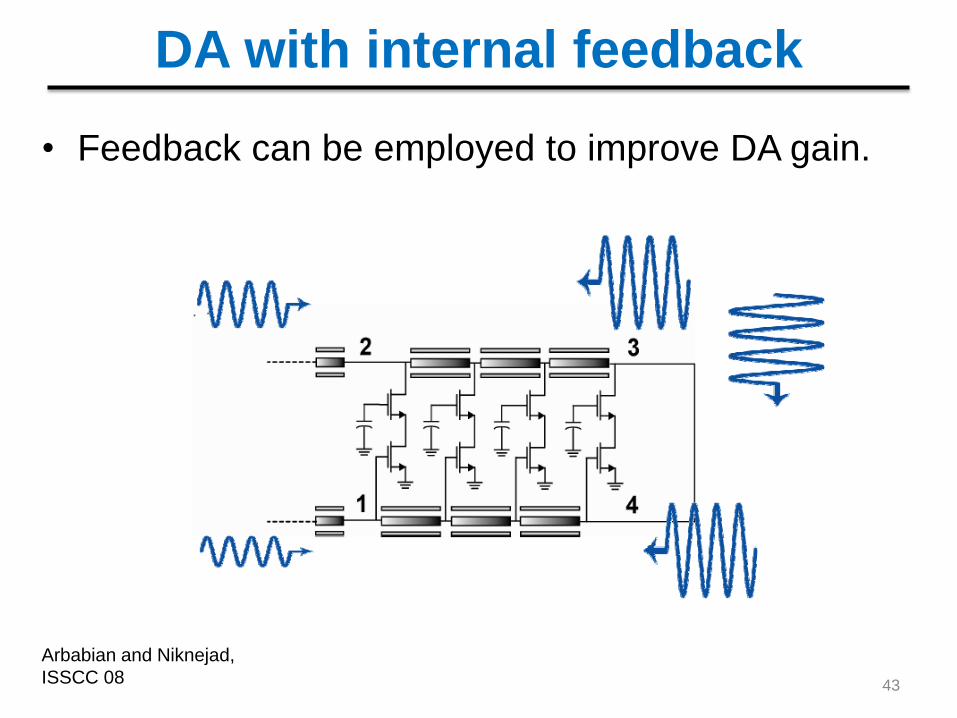
DA with internal feedback
• Feedback can be employed to improve DA gain.
43
Arbabian and Niknejad,
ISSCC 08
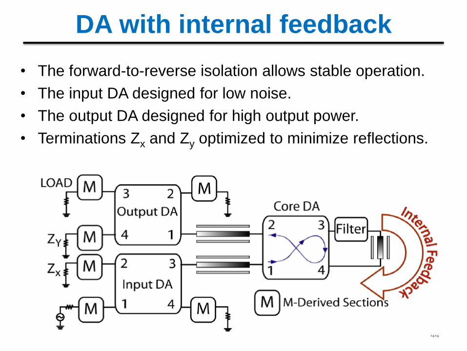
DA with internal feedback
• The forward-to-reverse isolation allows stable operation.
• The input DA designed for low noise.
• The output DA designed for high output power.
• Terminations Zx and Zy optimized to minimize reflections.
44
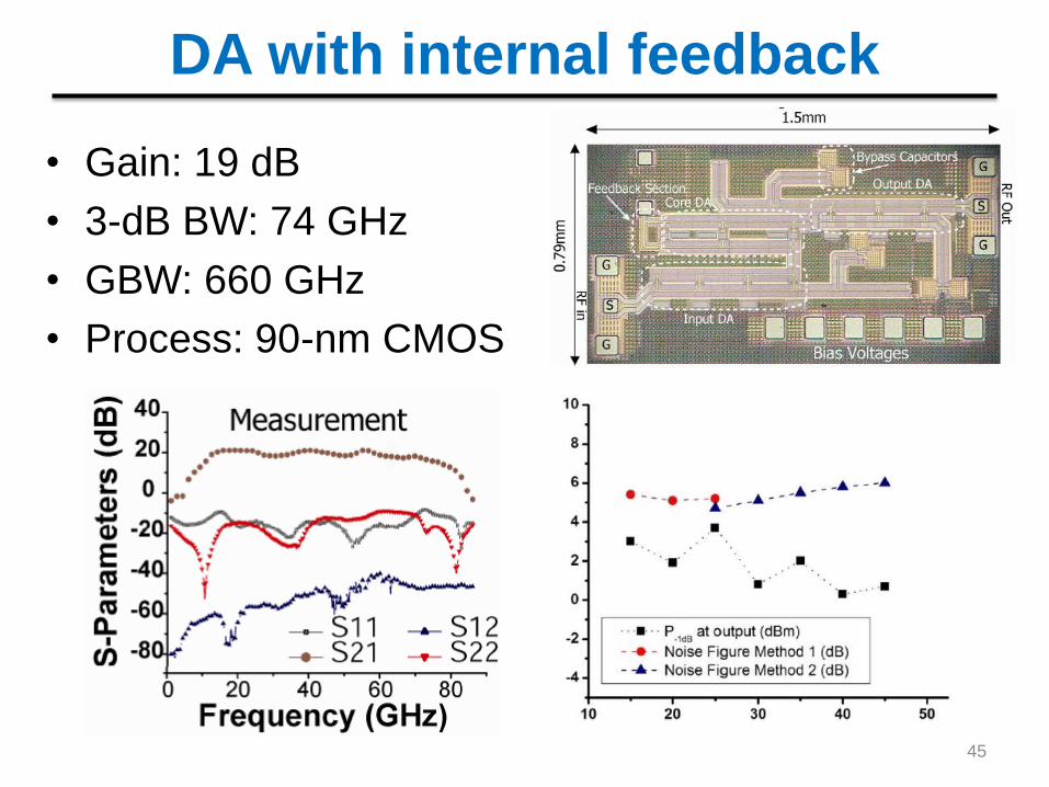
DA with internal feedback
• Gain: 19 dB
• 3-dB BW: 74 GHz
• GBW: 660 GHz
• Process: 90-nm CMOS
45
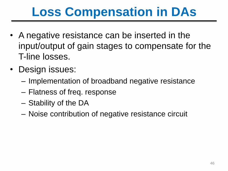
Loss Compensation in DAs
• A negative resistance can be inserted in the
input/output of gain stages to compensate for the
T-line losses.
• Design issues:
– Implementation of broadband negative resistance
– Flatness of freq. response
– Stability of the DA
– Noise contribution of negative resistance circuit
46
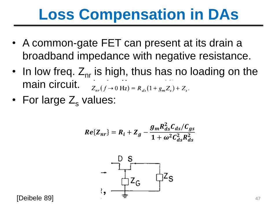
Loss Compensation in DAs
• A common-gate FET can present at its drain a
broadband impedance with negative resistance.
• In low freq. Znr is high, thus has no loading on the
main circuit.
• For large Zs values:
𝑹𝒆 𝒁𝒏𝒓 = 𝑹𝒊 + 𝒁𝒈 −𝒈𝒎𝑹𝒅𝒔
𝟐 𝑪𝒅𝒔/𝑪𝒈𝒔
𝟏 +𝝎𝟐𝑪𝒅𝒔𝟐 𝑹𝒅𝒔𝟐
47 [Deibele 89]
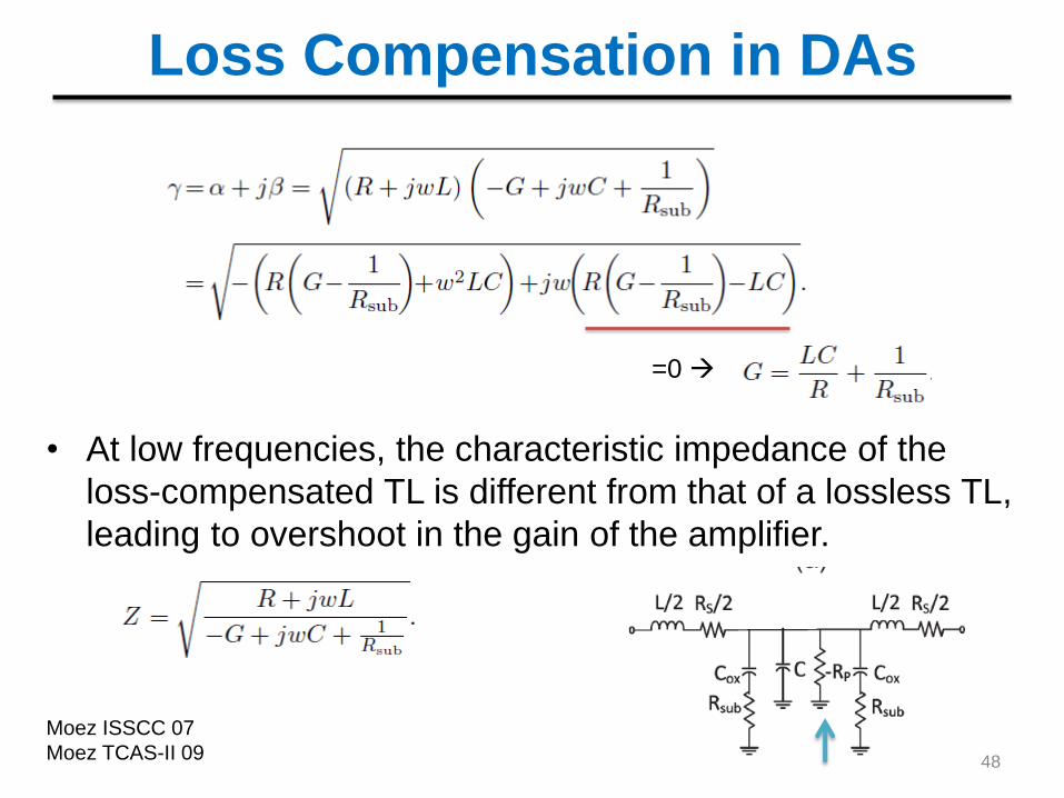
Loss Compensation in DAs
• At low frequencies, the characteristic impedance of the
loss-compensated TL is different from that of a lossless TL,
leading to overshoot in the gain of the amplifier.
48
=0
Moez ISSCC 07
Moez TCAS-II 09
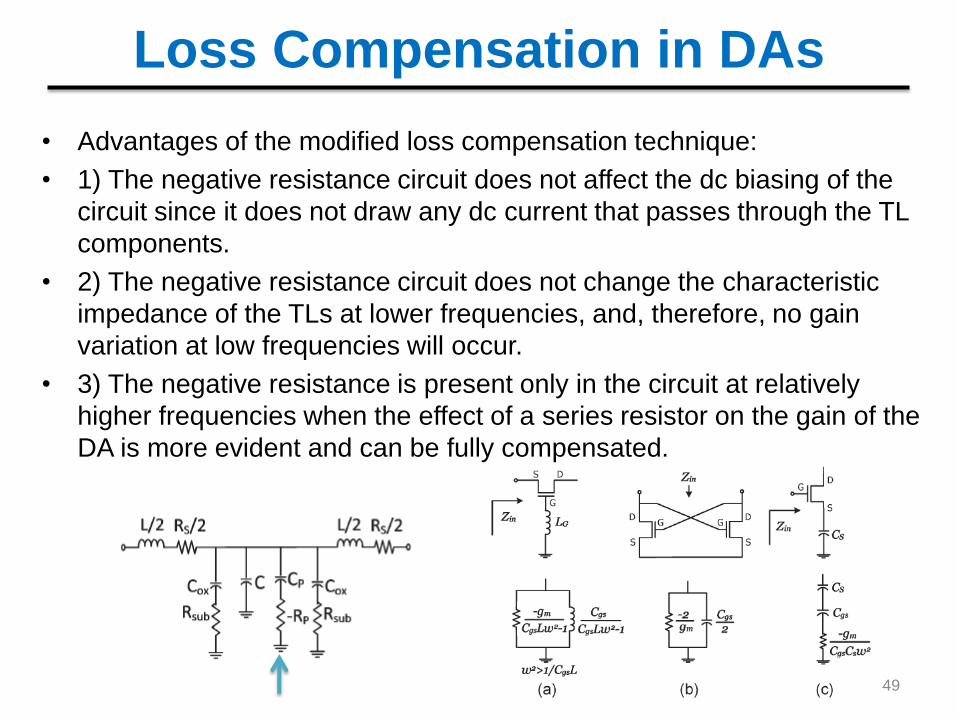
Loss Compensation in DAs
• Advantages of the modified loss compensation technique:
• 1) The negative resistance circuit does not affect the dc biasing of the
circuit since it does not draw any dc current that passes through the TL
components.
• 2) The negative resistance circuit does not change the characteristic
impedance of the TLs at lower frequencies, and, therefore, no gain
variation at low frequencies will occur.
• 3) The negative resistance is present only in the circuit at relatively
higher frequencies when the effect of a series resistor on the gain of the
DA is more evident and can be fully compensated.
49
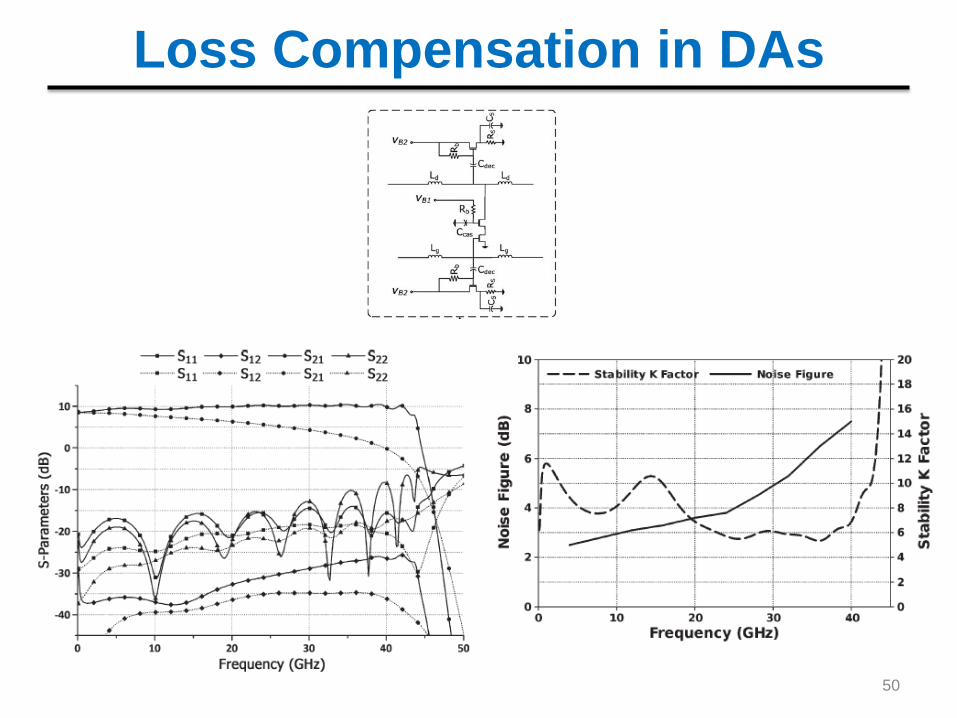
Loss Compensation in DAs
50
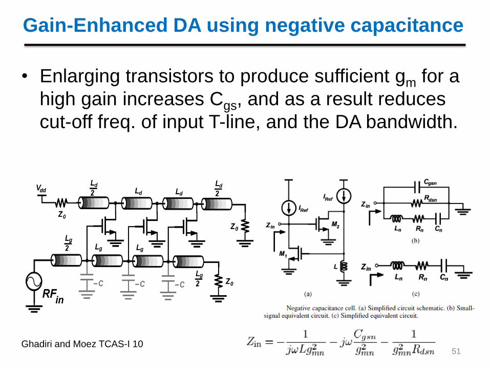
Gain-Enhanced DA using negative capacitance
• Enlarging transistors to produce sufficient gm for a
high gain increases Cgs, and as a result reduces
cut-off freq. of input T-line, and the DA bandwidth.
51 Ghadiri and Moez TCAS-I 10
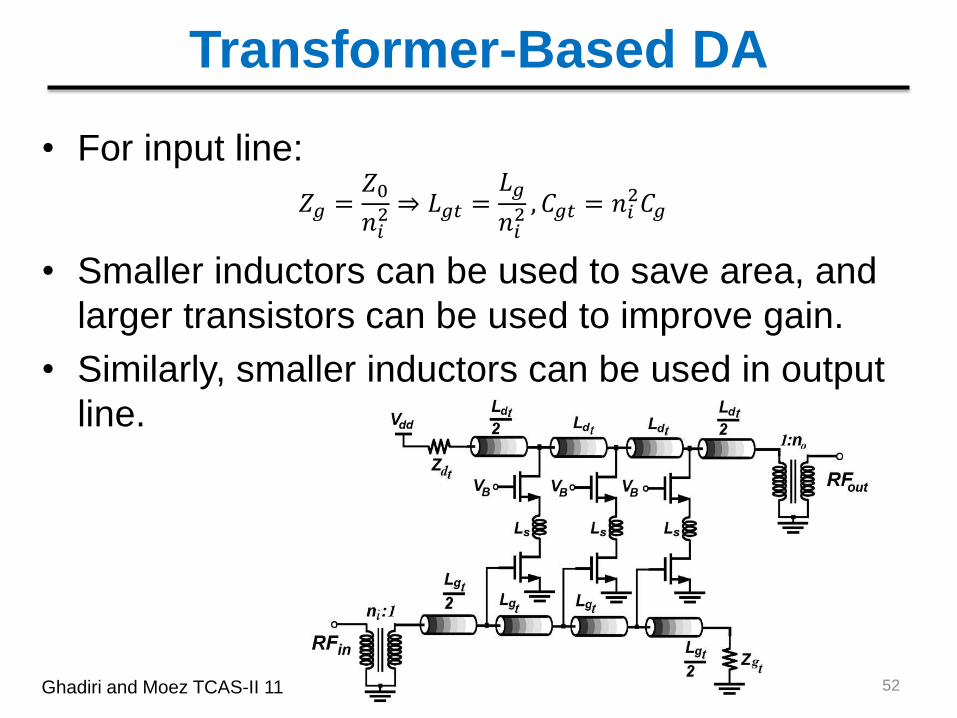
Transformer-Based DA
• For input line:
𝑍𝑔 =𝑍0
𝑛𝑖2 ⇒ 𝐿𝑔𝑡 =
𝐿𝑔
𝑛𝑖2 , 𝐶𝑔𝑡 = 𝑛𝑖
2𝐶𝑔
• Smaller inductors can be used to save area, and
larger transistors can be used to improve gain.
• Similarly, smaller inductors can be used in output
line.
52 Ghadiri and Moez TCAS-II 11
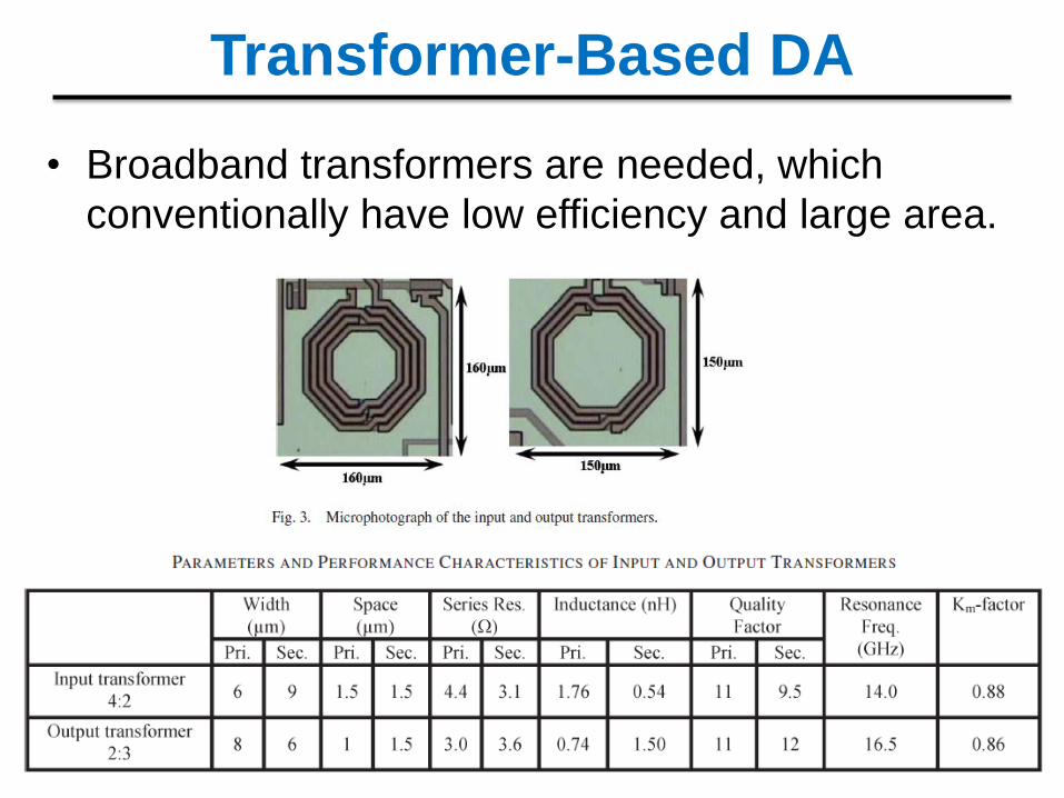
Transformer-Based DA
• Broadband transformers are needed, which
conventionally have low efficiency and large area.
53
Transformer-Based DA
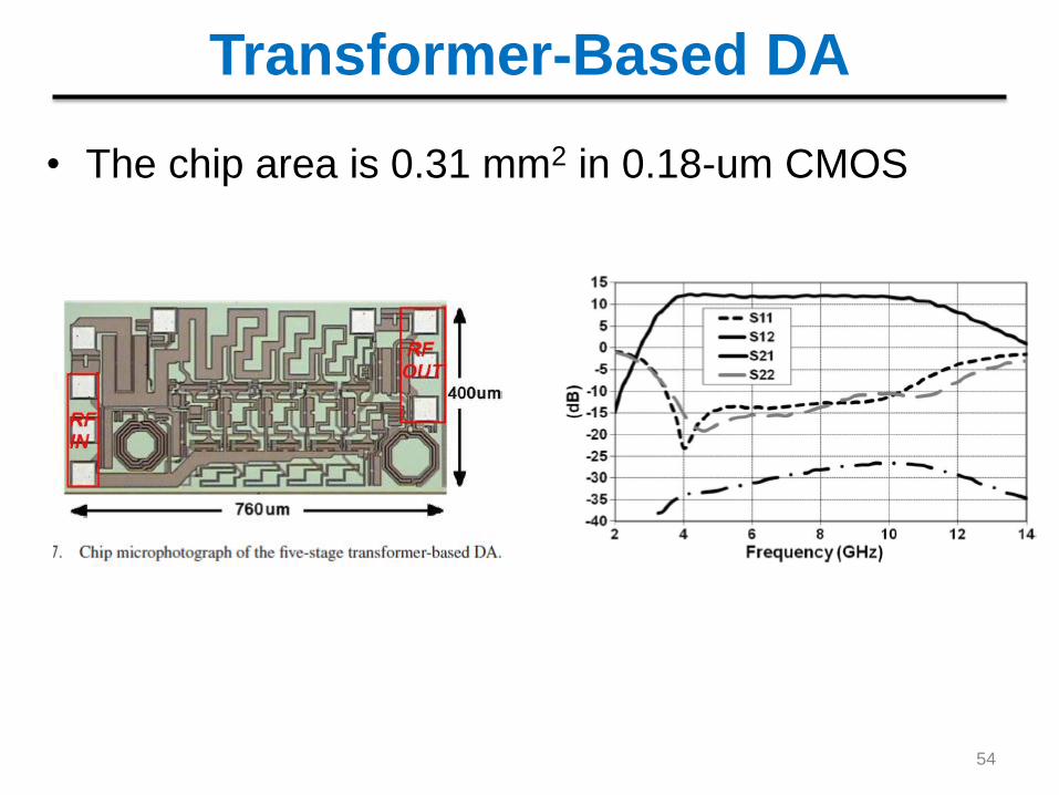
• The chip area is 0.31 mm2 in 0.18-um CMOS
54