Embed Size (px)
Citation preview
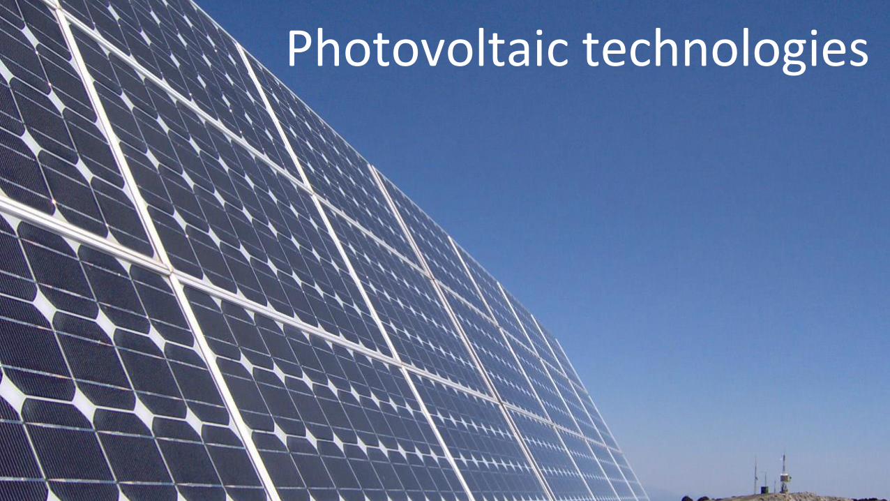
Photovoltaic technologies
Photovoltaic technologies
• Photovoltaic energy today
• Crystalline silicon technologies
• Limitations of crystalline silicon and monojunction solar cells
• Future PV technologies
PV energy today
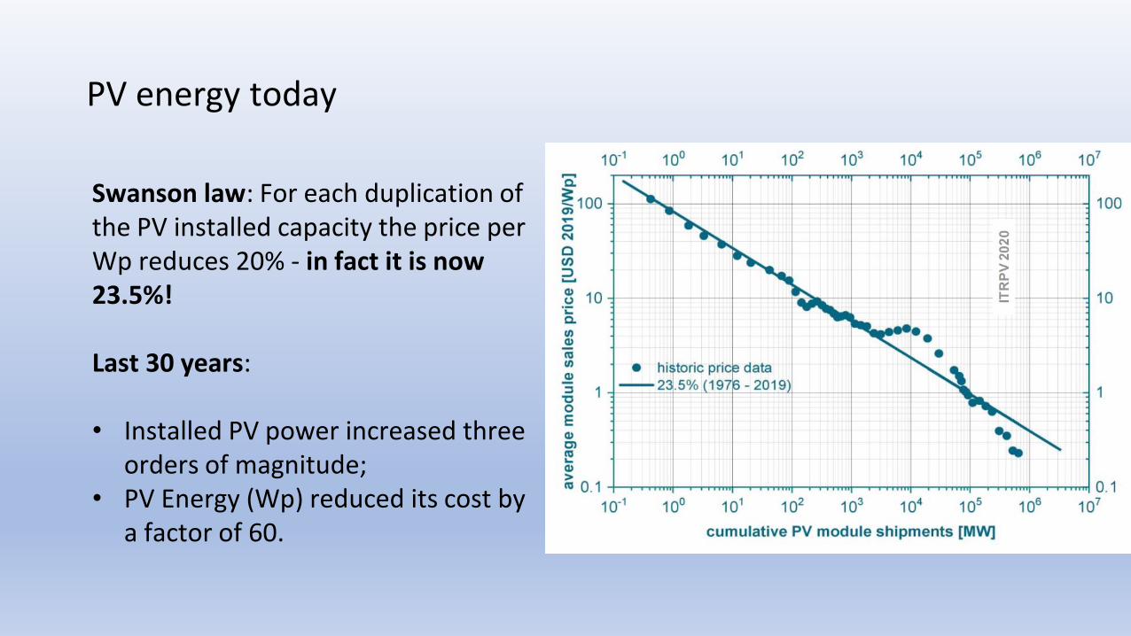
Swanson law: For each duplication of the PV installed capacity the price per Wp reduces 20% - in fact it is now 23.5%!
Last 30 years:
• Installed PV power increased three orders of magnitude;
• PV Energy (Wp) reduced its cost by a factor of 60.
PV energy today
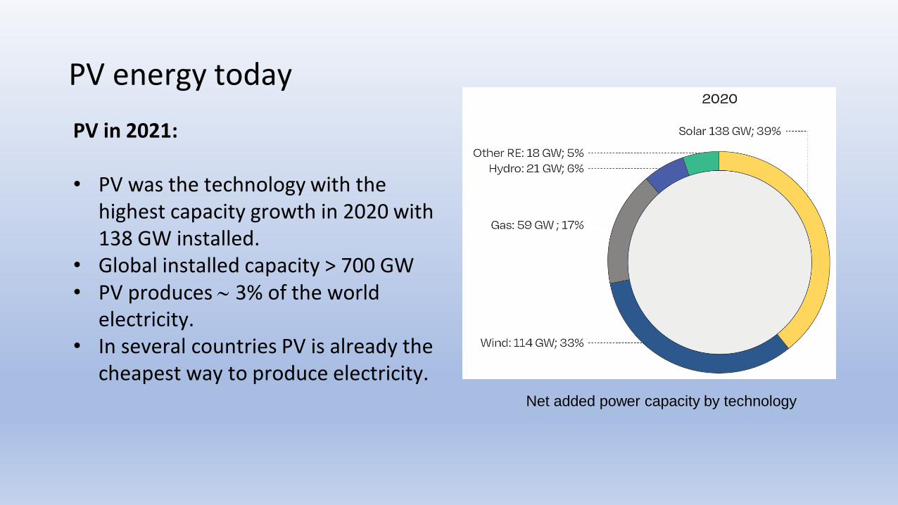
PV in 2021:
• PV was the technology with the highest capacity growth in 2020 with 138 GW installed.
• Global installed capacity > 700 GW • PV produces 3% of the world
electricity. • In several countries PV is already the
cheapest way to produce electricity.Net added power capacity by technology
Crystalline Silicon solar cell technologies
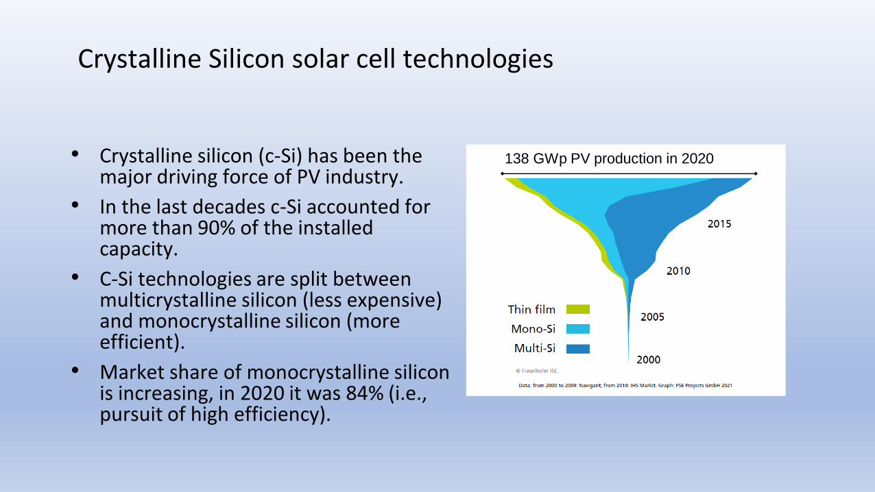
• Crystalline silicon (c-Si) has been the major driving force of PV industry.
• In the last decades c-Si accounted for more than 90% of the installed capacity.
• C-Si technologies are split between multicrystalline silicon (less expensive) and monocrystalline silicon (more efficient).
• Market share of monocrystalline silicon is increasing, in 2020 it was 84% (i.e., pursuit of high efficiency).
138 GWp PV production in 2020
Crystalline Silicon solar cell technologies
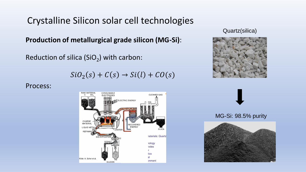
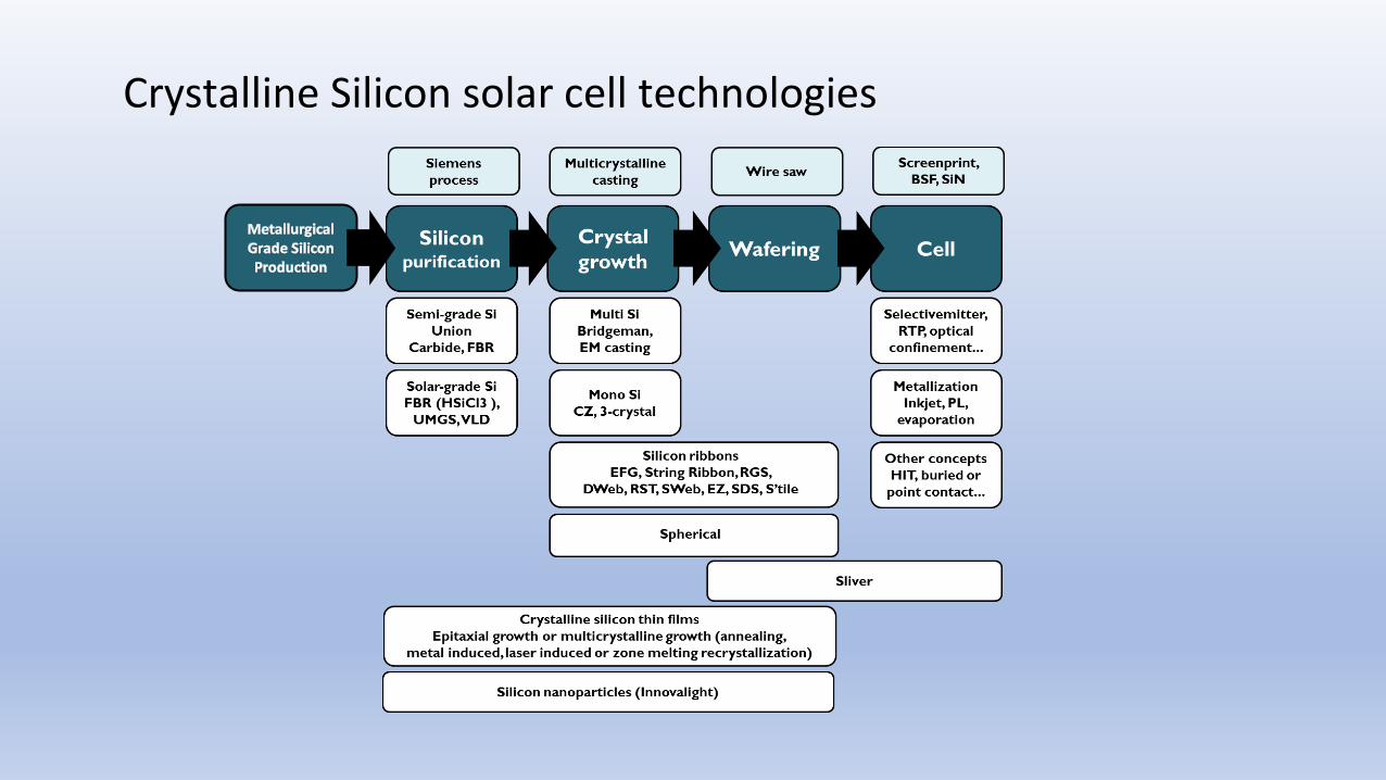
Production of metallurgical grade silicon (MG-Si):
Reduction of silica (SiO2) with carbon:
𝑆𝑖𝑂2 𝑠 + 𝐶 𝑠 → 𝑆𝑖 𝑙 + 𝐶𝑂(𝑠)
Process:
Crystalline Silicon solar cell technologies
MG-Si: 98.5% purity
Quartz(silica)
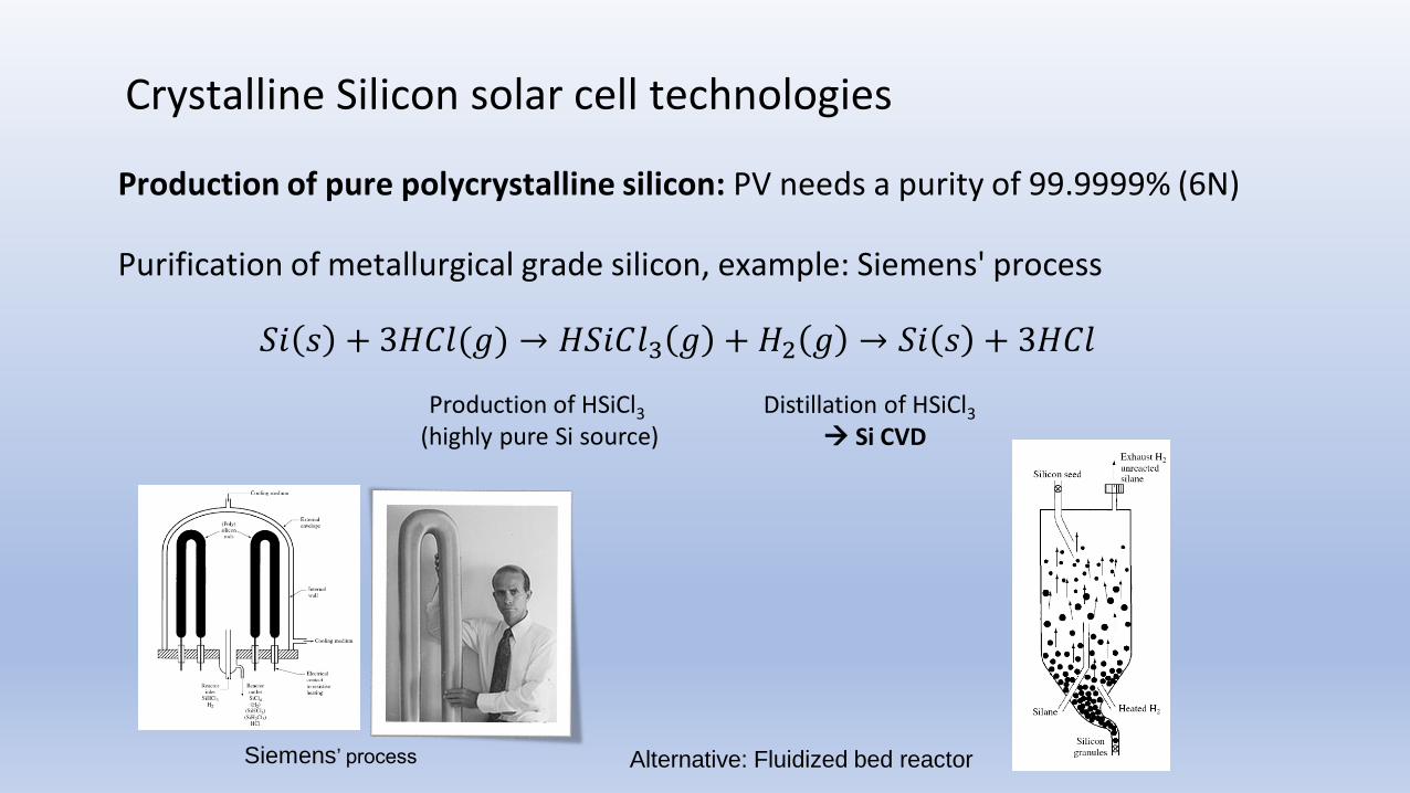
Production of pure polycrystalline silicon: PV needs a purity of 99.9999% (6N)
Purification of metallurgical grade silicon, example: Siemens' process
Crystalline Silicon solar cell technologies
Siemens’ process Alternative: Fluidized bed reactor
Production of HSiCl3
(highly pure Si source)
𝑆𝑖 𝑠 + 3𝐻𝐶𝑙(𝑔) → 𝐻𝑆𝑖𝐶𝑙3 𝑔 + 𝐻2 𝑔 → 𝑆𝑖 𝑠 + 3𝐻𝐶𝑙
Distillation of HSiCl3
→ Si CVD
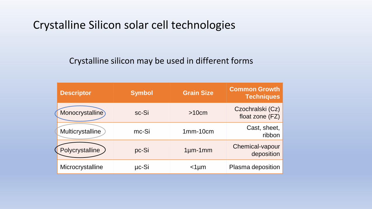
Crystalline silicon may be used in different forms
Crystalline Silicon solar cell technologies
Descriptor Symbol Grain SizeCommon Growth
Techniques
Monocrystalline sc-Si >10cmCzochralski (Cz)
float zone (FZ)
Multicrystalline mc-Si 1mm-10cmCast, sheet,
ribbon
Polycrystalline pc-Si 1µm-1mmChemical-vapour
deposition
Microcrystalline µc-Si <1µm Plasma deposition
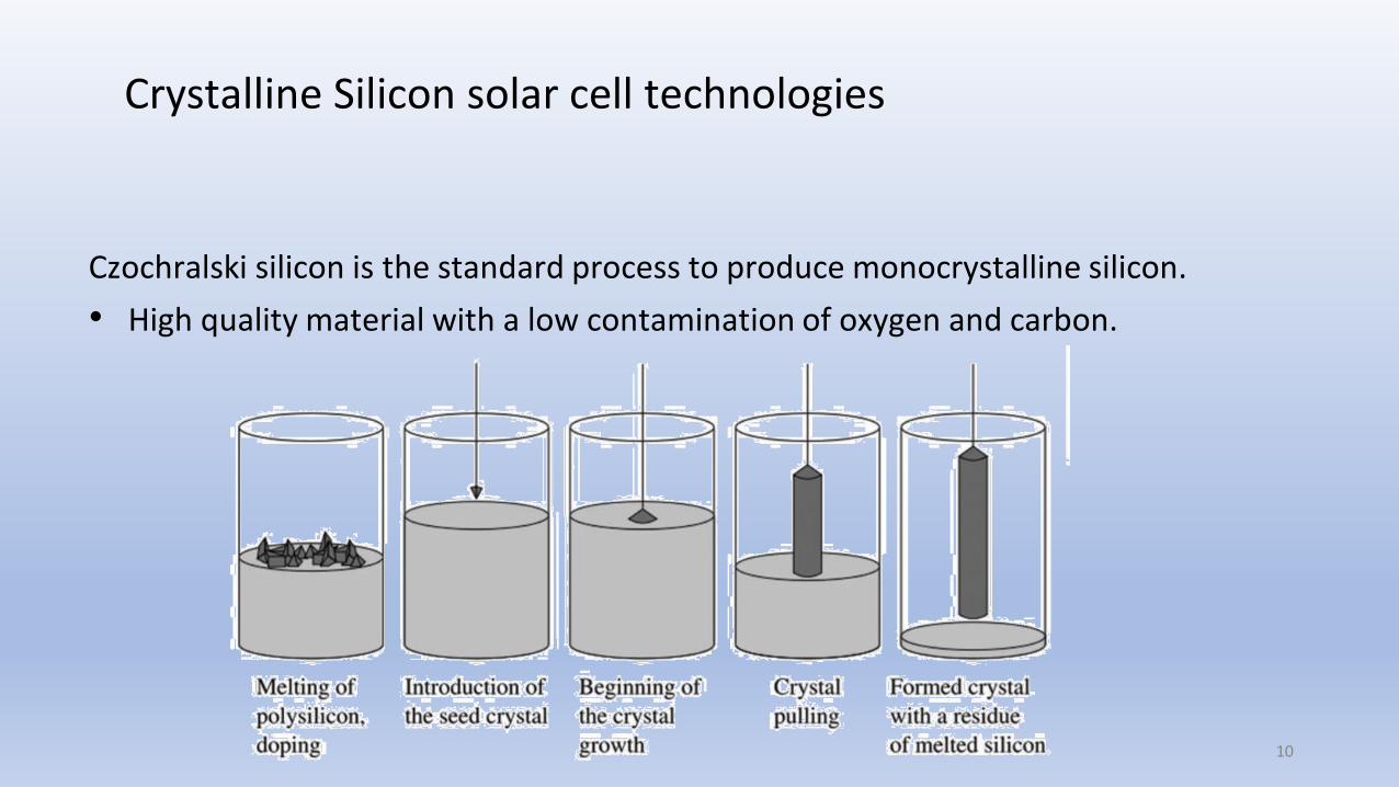
Czochralski silicon is the standard process to produce monocrystalline silicon.
• High quality material with a low contamination of oxygen and carbon.
10
Crystalline Silicon solar cell technologies
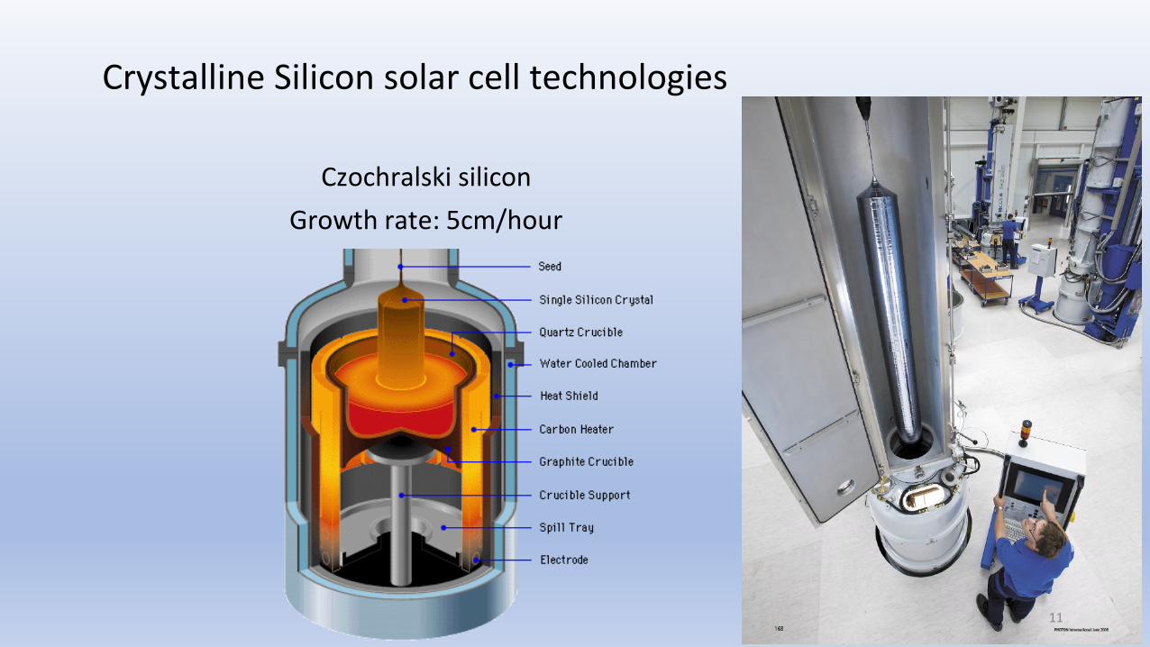
Czochralski silicon
Growth rate: 5cm/hour
11
Crystalline Silicon solar cell technologies
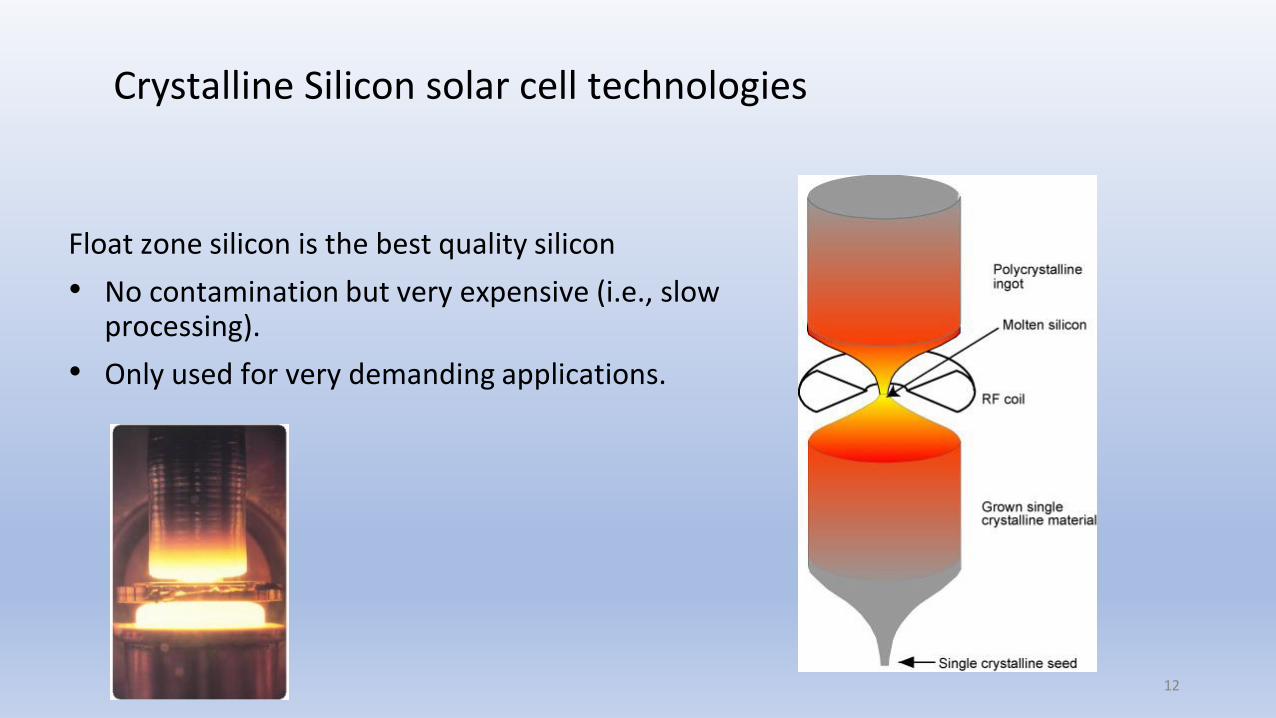
Float zone silicon is the best quality silicon
• No contamination but very expensive (i.e., slow processing).
• Only used for very demanding applications.
12
Crystalline Silicon solar cell technologies
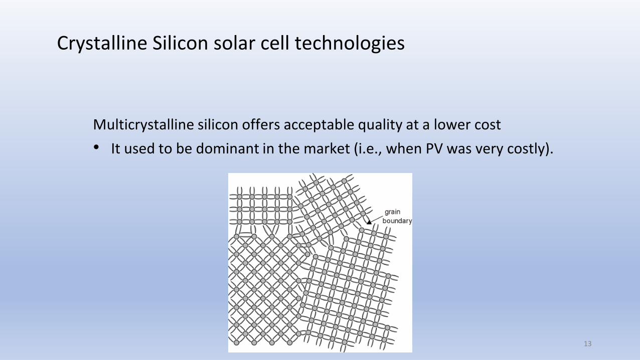
Multicrystalline silicon offers acceptable quality at a lower cost
• It used to be dominant in the market (i.e., when PV was very costly).
13
Crystalline Silicon solar cell technologies
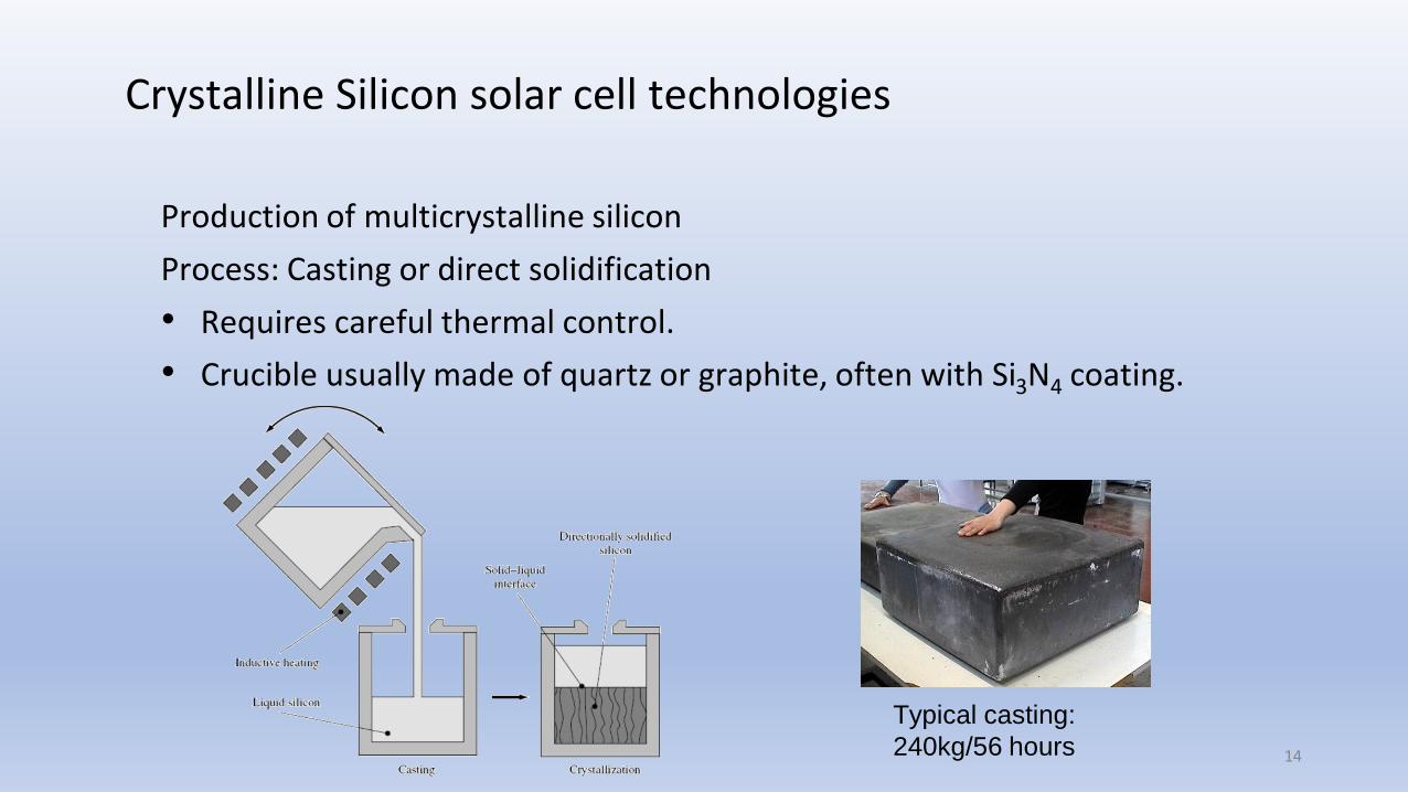
Production of multicrystalline silicon
Process: Casting or direct solidification
• Requires careful thermal control.
• Crucible usually made of quartz or graphite, often with Si3N4 coating.
Typical casting:
240kg/56 hours 14
Crystalline Silicon solar cell technologies
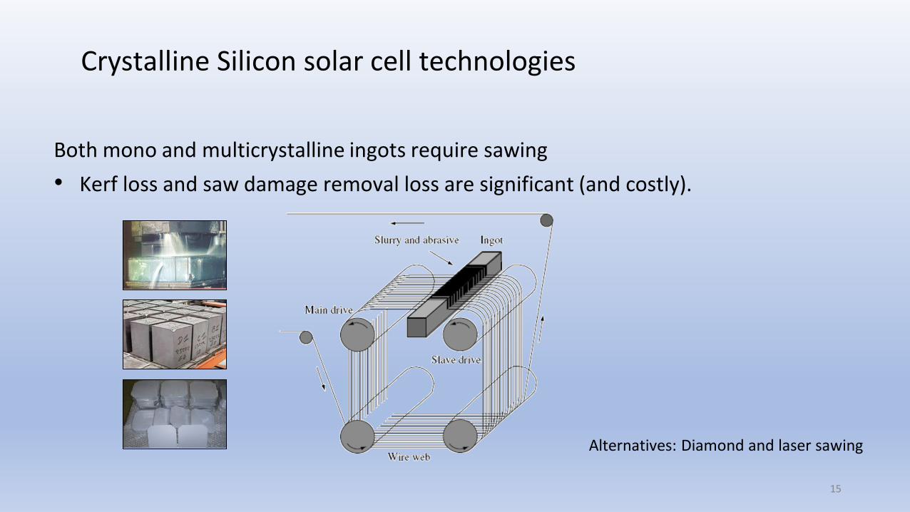
Both mono and multicrystalline ingots require sawing
• Kerf loss and saw damage removal loss are significant (and costly).
15
Crystalline Silicon solar cell technologies
Alternatives: Diamond and laser sawing
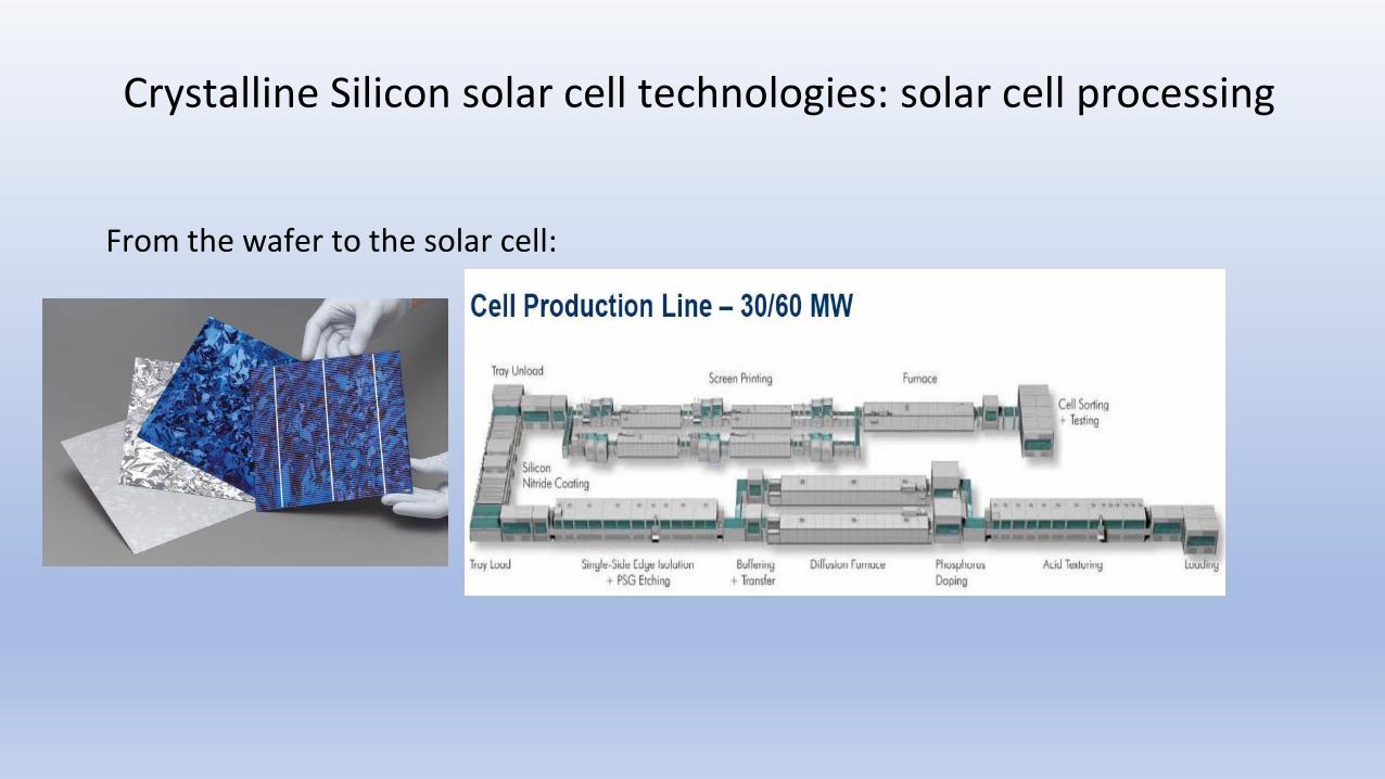
From the wafer to the solar cell:
Crystalline Silicon solar cell technologies: solar cell processing
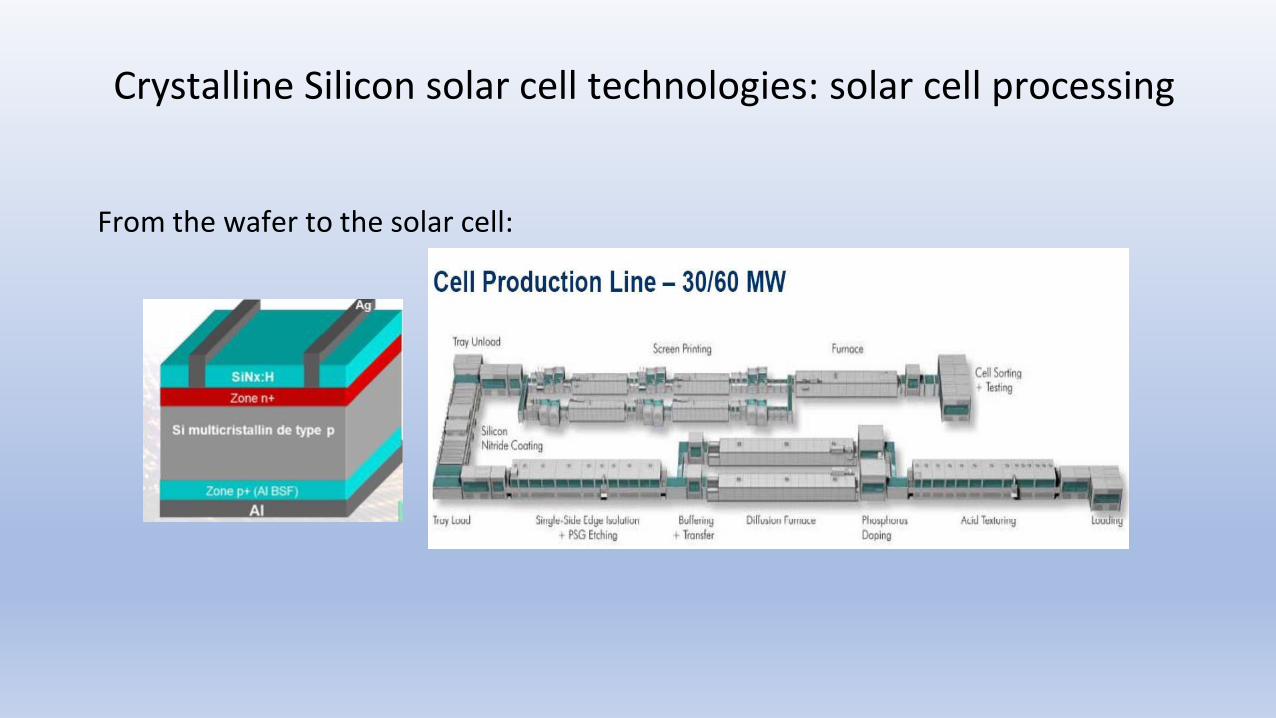
From the wafer to the solar cell:
Crystalline Silicon solar cell technologies: solar cell processing
18
Crystalline Silicon solar cell technologies: solar cell processing
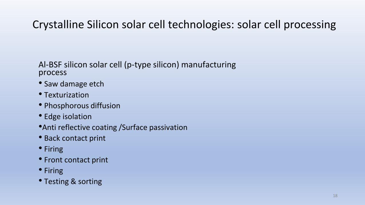
Al-BSF silicon solar cell (p-type silicon) manufacturing process• Saw damage etch
• Texturization
• Phosphorous diffusion
• Edge isolation
•Anti reflective coating /Surface passivation
• Back contact print
• Firing
• Front contact print
• Firing
• Testing & sorting
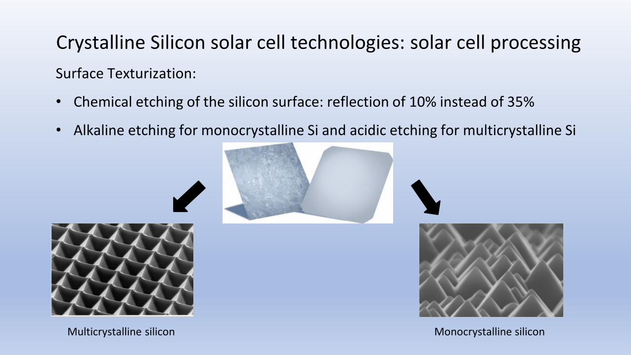
Surface Texturization:
• Chemical etching of the silicon surface: reflection of 10% instead of 35%
• Alkaline etching for monocrystalline Si and acidic etching for multicrystalline Si
Crystalline Silicon solar cell technologies: solar cell processing
Multicrystalline silicon Monocrystalline silicon
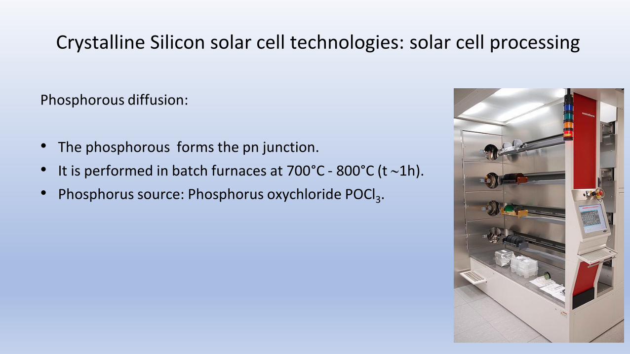
Phosphorous diffusion:
• The phosphorous forms the pn junction.
• It is performed in batch furnaces at 700°C - 800°C (t 1h).
• Phosphorus source: Phosphorus oxychloride POCl3.
Crystalline Silicon solar cell technologies: solar cell processing
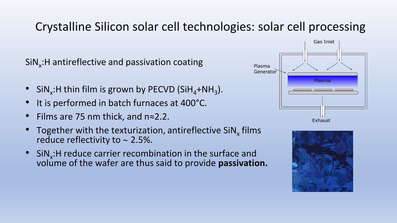
SiNx:H antireflective and passivation coating
• SiNx:H thin film is grown by PECVD (SiH4+NH3).
• It is performed in batch furnaces at 400°C.
• Films are 75 nm thick, and n≈2.2.
• Together with the texturization, antireflective SiNx films reduce reflectivity to 2.5%.
• SiNx:H reduce carrier recombination in the surface and volume of the wafer are thus said to provide passivation.
Crystalline Silicon solar cell technologies: solar cell processing
Crystalline Silicon solar cell technologies: solar cell processing
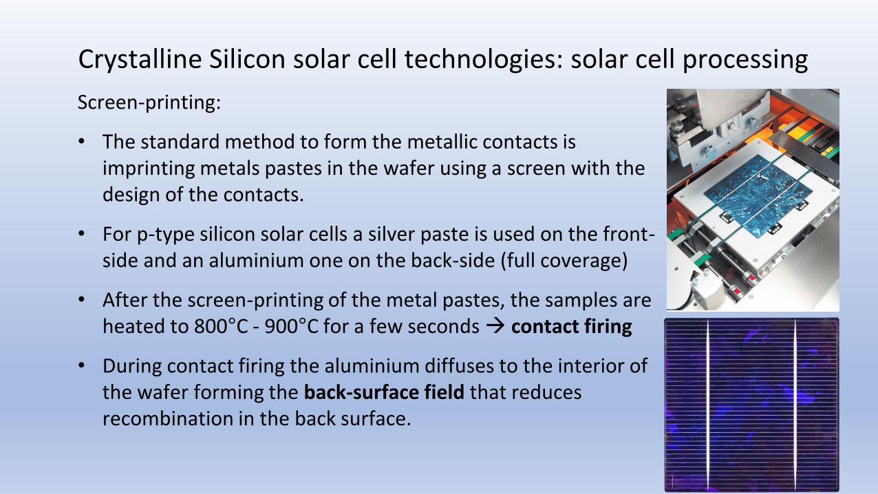
Screen-printing:
• The standard method to form the metallic contacts is imprinting metals pastes in the wafer using a screen with the design of the contacts.
• For p-type silicon solar cells a silver paste is used on the front-side and an aluminium one on the back-side (full coverage)
• After the screen-printing of the metal pastes, the samples are heated to 800°C - 900°C for a few seconds → contact firing
• During contact firing the aluminium diffuses to the interior of the wafer forming the back-surface field that reduces recombination in the back surface.
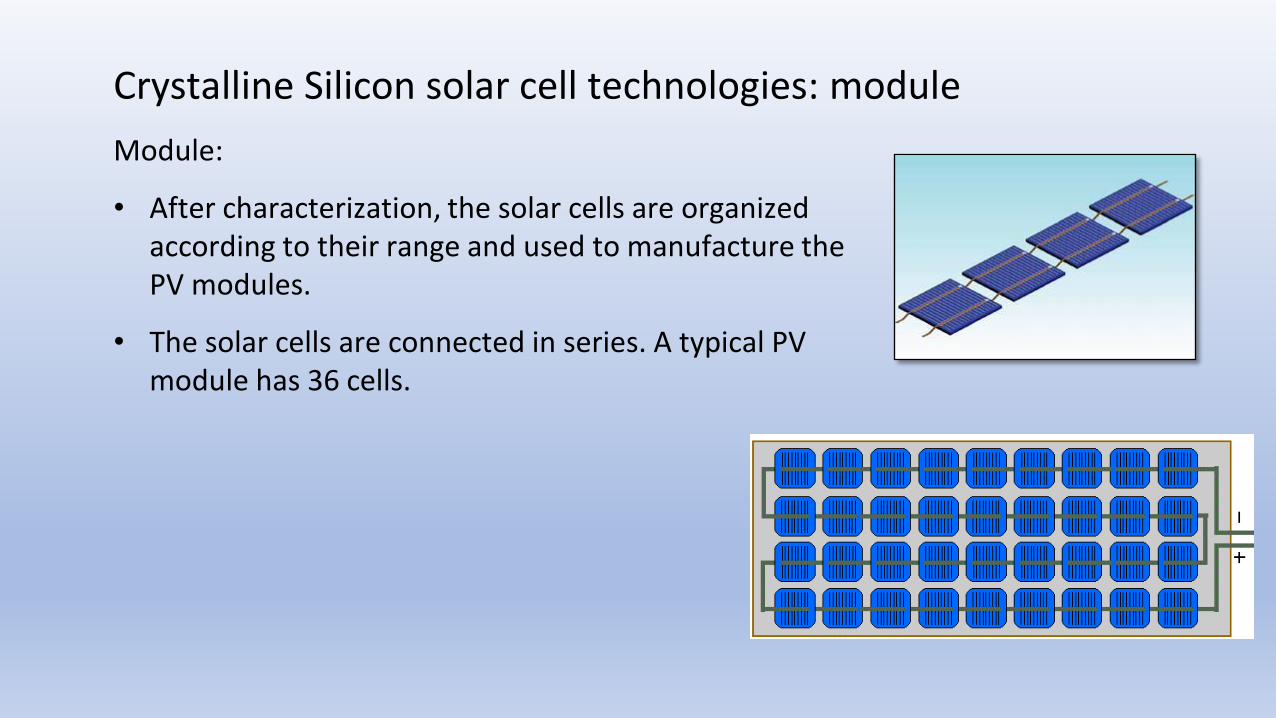
Crystalline Silicon solar cell technologies: module
Module:
• After characterization, the solar cells are organized according to their range and used to manufacture the PV modules.
• The solar cells are connected in series. A typical PV module has 36 cells.
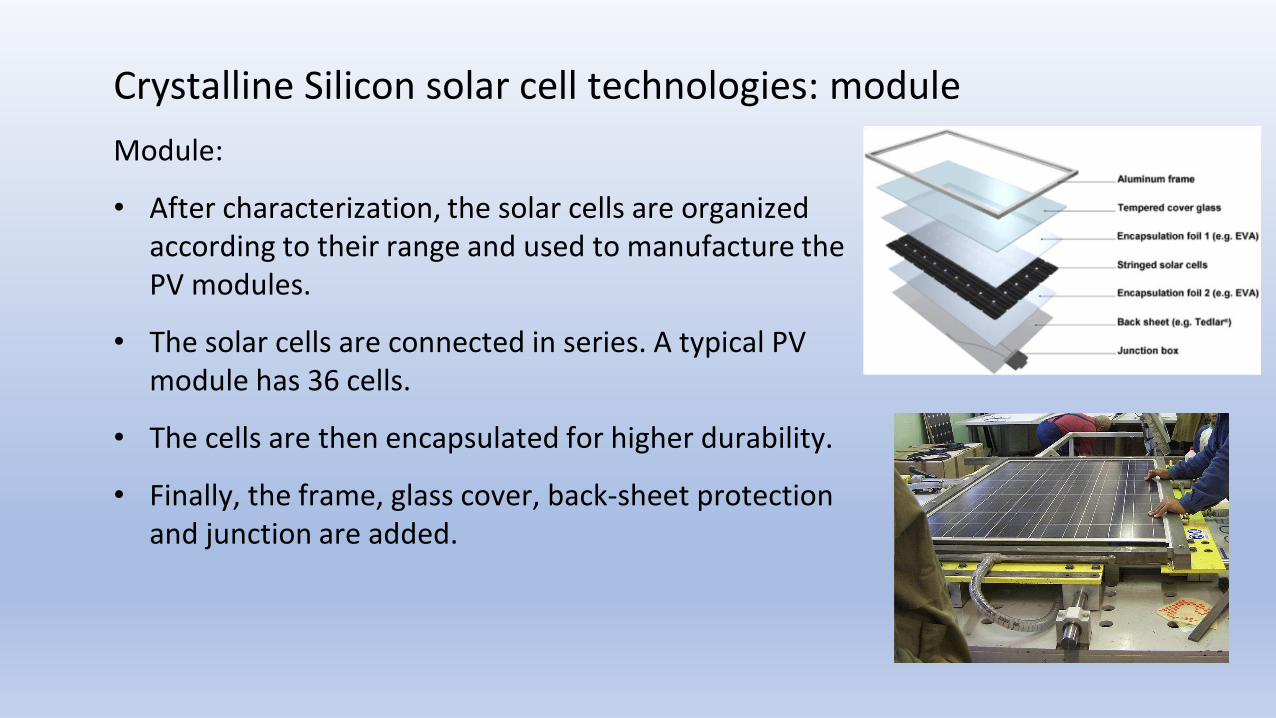
Crystalline Silicon solar cell technologies: module
Module:
• After characterization, the solar cells are organized according to their range and used to manufacture the PV modules.
• The solar cells are connected in series. A typical PV module has 36 cells.
• The cells are then encapsulated for higher durability.
• Finally, the frame, glass cover, back-sheet protection and junction are added.
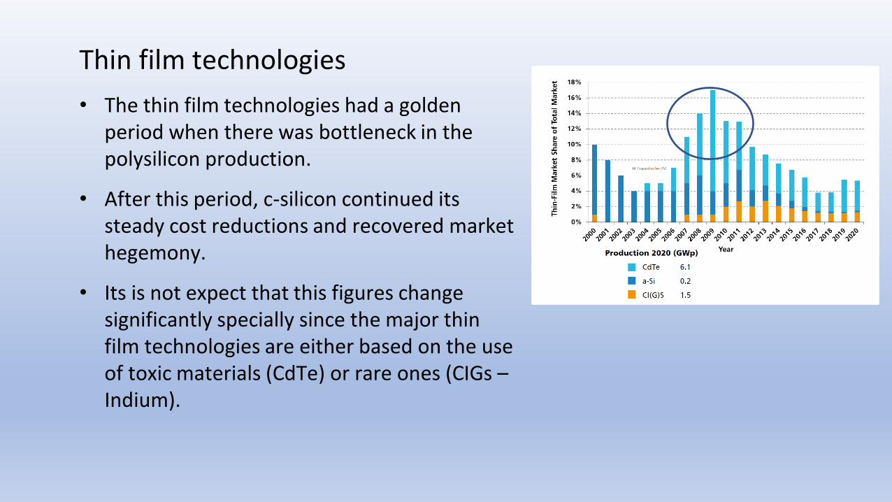
Thin film technologies
• The thin film technologies had a golden period when there was bottleneck in the polysilicon production.
• After this period, c-silicon continued its steady cost reductions and recovered market hegemony.
• Its is not expect that this figures change significantly specially since the major thin film technologies are either based on the use of toxic materials (CdTe) or rare ones (CIGs –Indium).
Limitations of crystalline silicon and monojunction solar cells
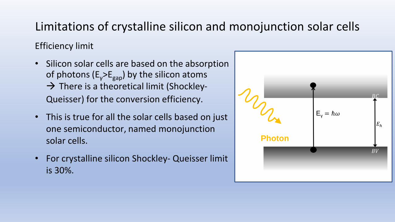
Efficiency limit
• Silicon solar cells are based on the absorption of photons (Eγ>Egap) by the silicon atoms → There is a theoretical limit (Shockley-
Queisser) for the conversion efficiency.
• This is true for all the solar cells based on just one semiconductor, named monojunctionsolar cells.
• For crystalline silicon Shockley- Queisser limit is 30%.
Eγ = ℏ𝜔
Photon
𝐵𝐶
𝐵𝑉
𝐸ℎ
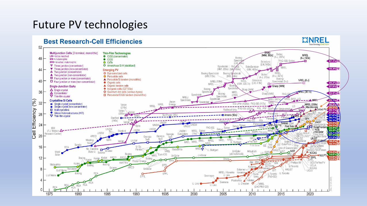
Future PV technologies
Future PV technologies
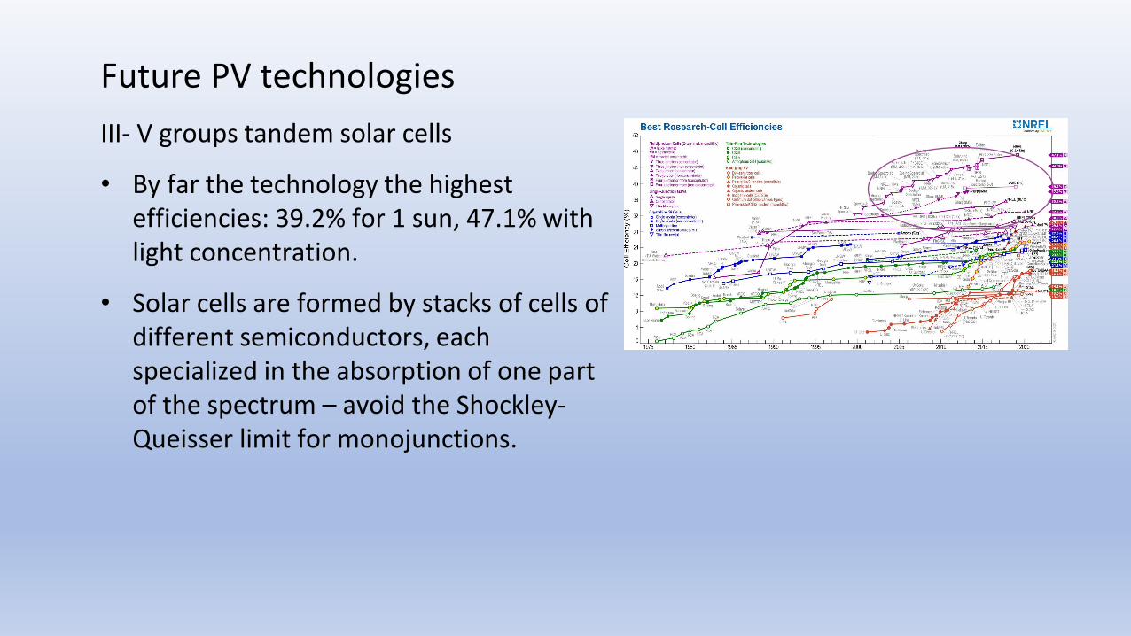
III- V groups tandem solar cells
• By far the technology the highest efficiencies: 39.2% for 1 sun, 47.1% with light concentration.
• Solar cells are formed by stacks of cells of different semiconductors, each specialized in the absorption of one part of the spectrum – avoid the Shockley-Queisser limit for monojunctions.
Future PV technologies
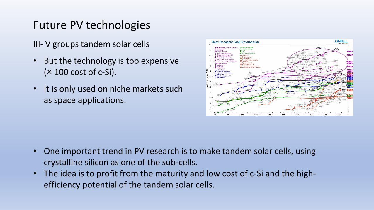
III- V groups tandem solar cells
• But the technology is too expensive (× 100 cost of c-Si).
• It is only used on niche markets such as space applications.
• One important trend in PV research is to make tandem solar cells, using crystalline silicon as one of the sub-cells.
• The idea is to profit from the maturity and low cost of c-Si and the high-efficiency potential of the tandem solar cells.
Future PV technologies
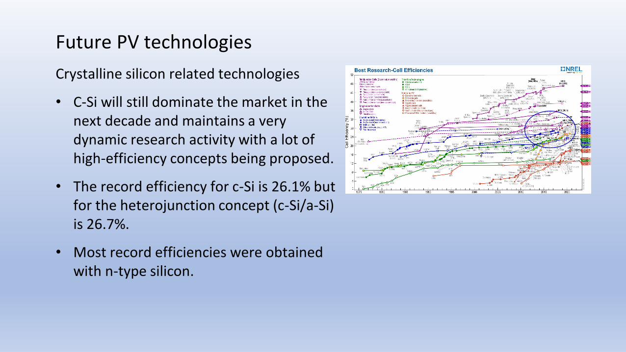
Crystalline silicon related technologies
• C-Si will still dominate the market in the next decade and maintains a very dynamic research activity with a lot of high-efficiency concepts being proposed.
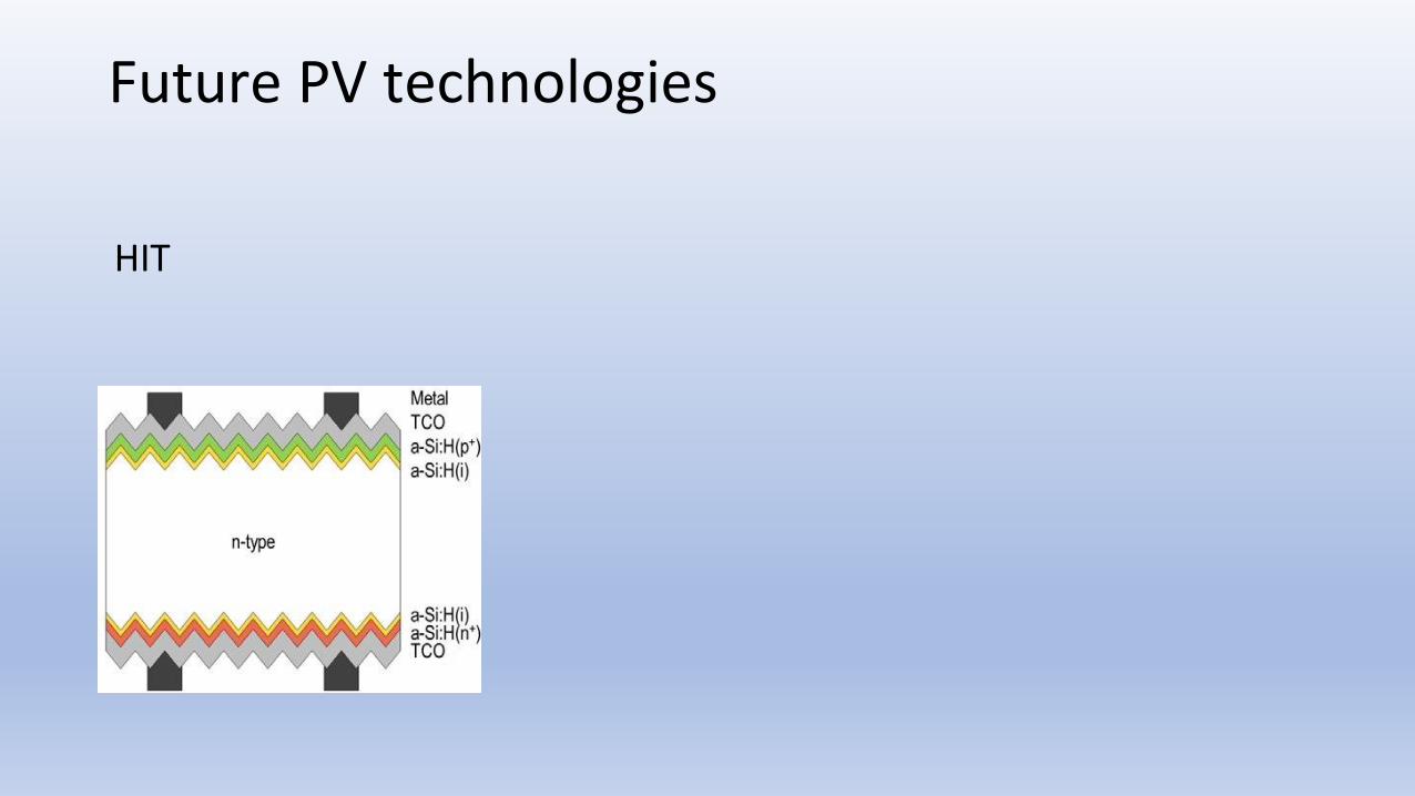
• The record efficiency for c-Si is 26.1% but for the heterojunction concept (c-Si/a-Si) is 26.7%.
• Most record efficiencies were obtained with n-type silicon.
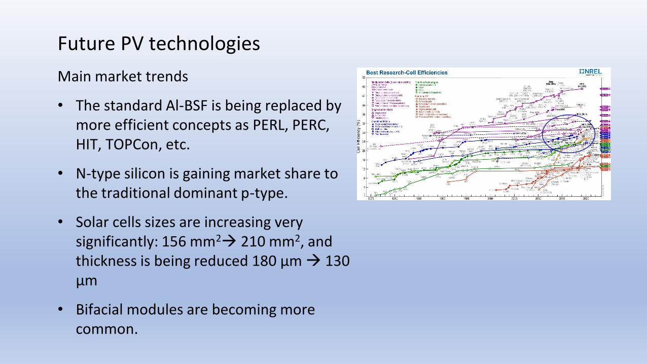
Future PV technologies
Main market trends
• The standard Al-BSF is being replaced by more efficient concepts as PERL, PERC, HIT, TOPCon, etc.
• N-type silicon is gaining market share to the traditional dominant p-type.
• Solar cells sizes are increasing very significantly: 156 mm2
→ 210 mm2, and thickness is being reduced 180 μm → 130μm
• Bifacial modules are becoming more common.
Future PV technologies
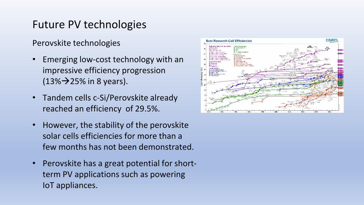
Perovskite technologies
• Emerging low-cost technology with an impressive efficiency progression (13%→25% in 8 years).
• Tandem cells c-Si/Perovskite already reached an efficiency of 29.5%.
• However, the stability of the perovskite solar cells efficiencies for more than a few months has not been demonstrated.
• Perovskite has a great potential for short-term PV applications such as powering IoT appliances.
Future PV technologies
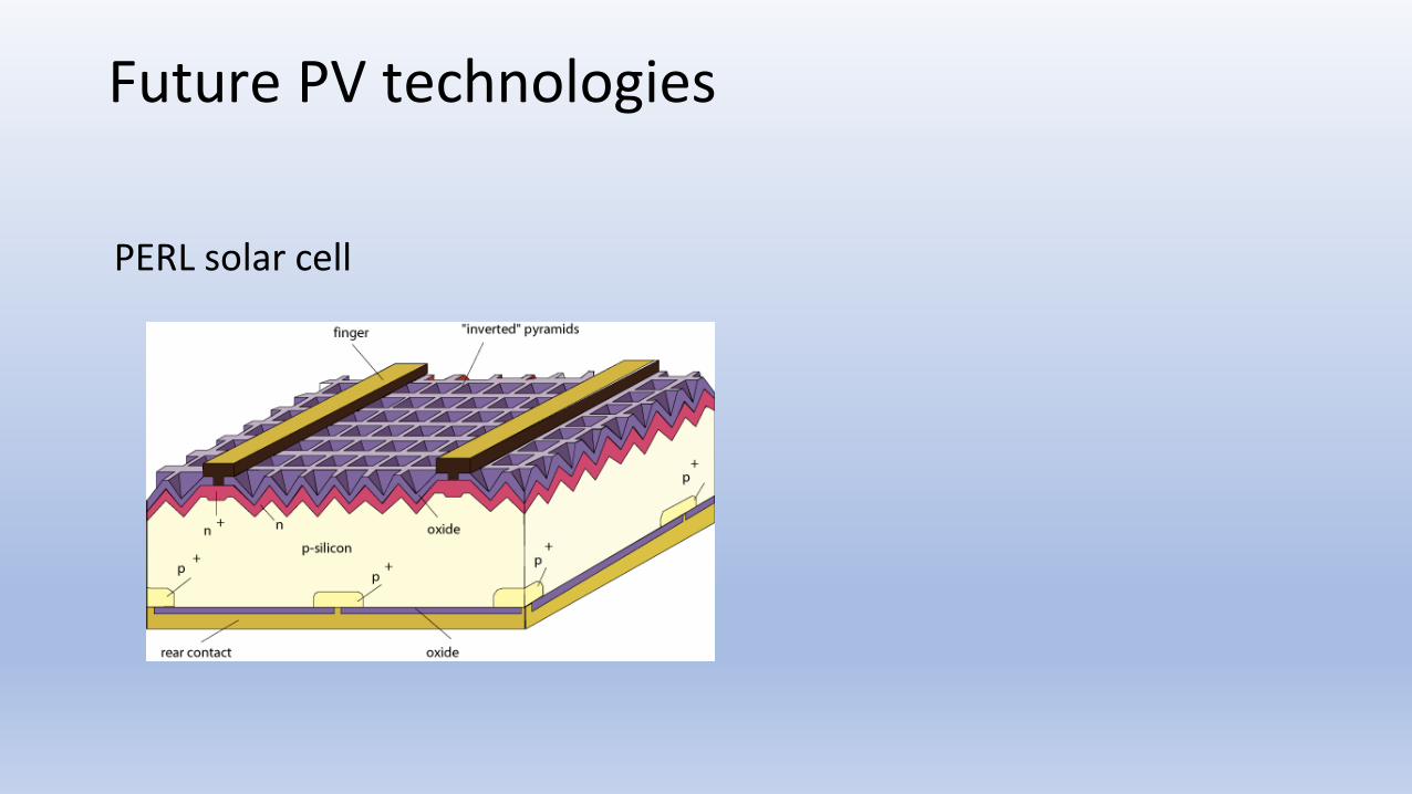
PERL solar cell
Future PV technologies
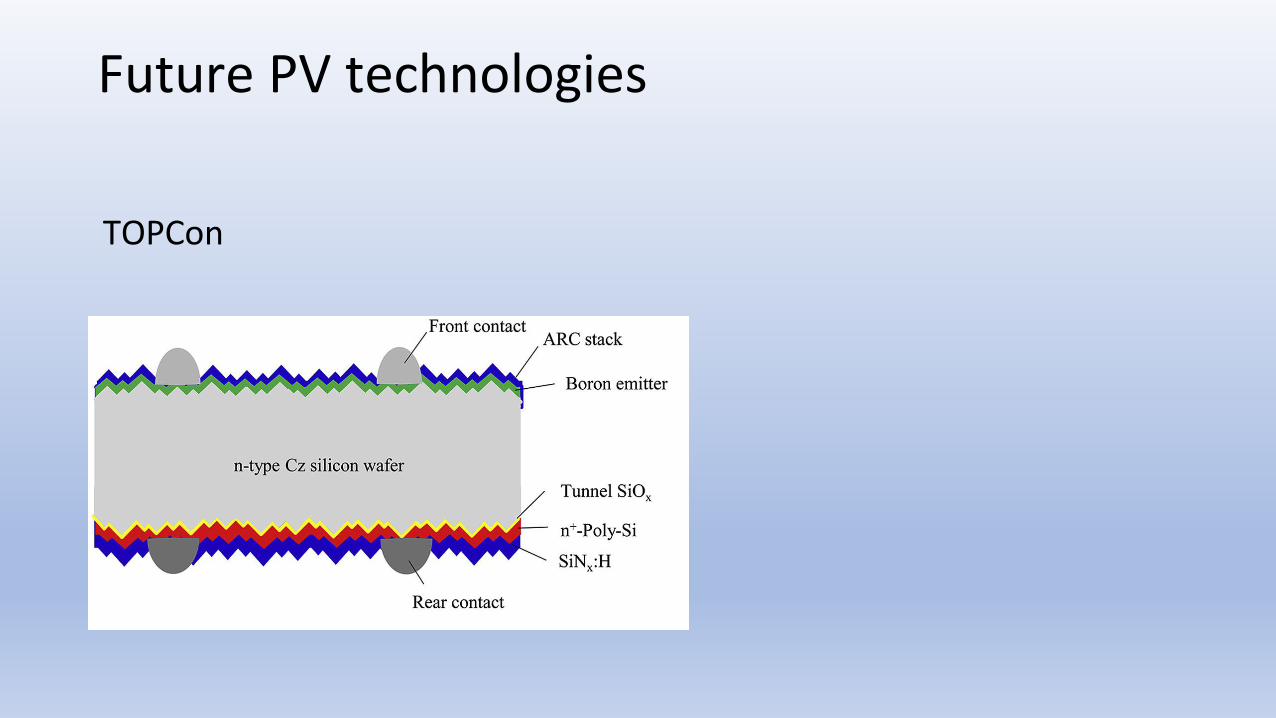
TOPCon
Future PV technologies
HIT