Embed Size (px)
Citation preview
VOLUME 64, NUMBER 16 PHYSICAL REVIEW LETTERS 16 APRIL 1990
Dislocation-Free Stranski-Krastanow Growth of Ge on Si(1QQ)
D. J. Eaglesham and M. CerulloA Td'c T Bell Laboratories, 600 Mountain Avenue, Murray Hill, New Jersey 07974
(Received 27 December 1989)
We show that the islands formed in Stranski-Krastanow (SK) growth of Ge on Si(100) are initiallydislocation free -Isla. nd formation in true SK growth should be driven by strain relaxation in large,dislocated islands. Coherent SK growth is explained in terms of elastic deformation around the islands,which partially accommodates mismatch. The limiting critical thickness, h„ofcoherent SK islands isshown to be higher than that for 2D growth. We demonstrate growth of dislocation-free Ge islands onSi to a thickness of = 500 A, 50 X higher than h„for 2D Ge/Si epitaxy.
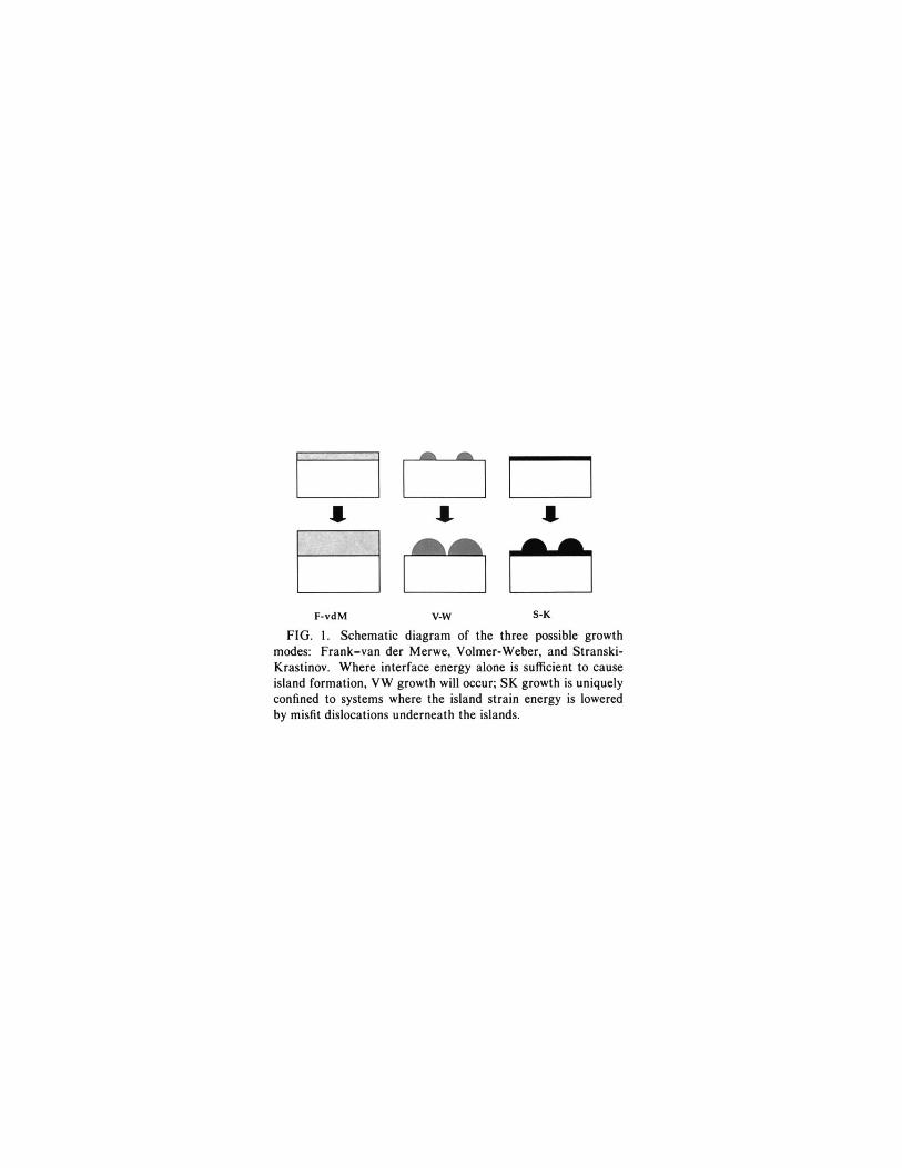
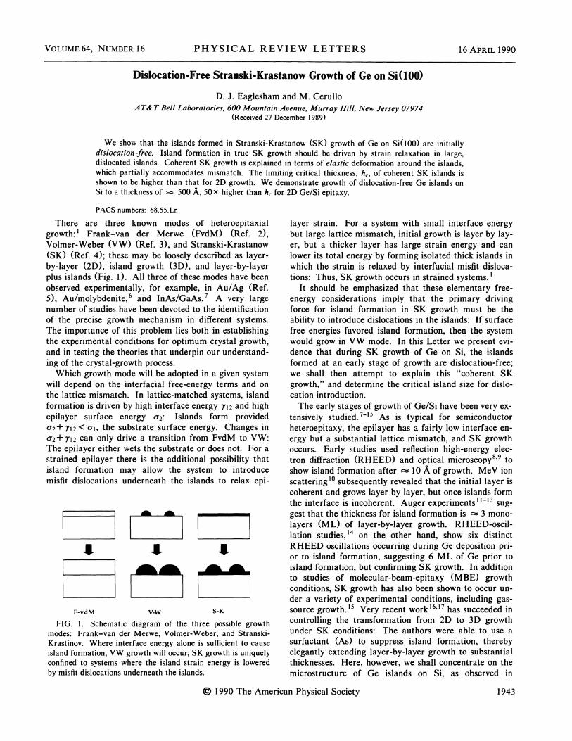
F-vdM V-%V S-K
FIG. 1. Schematic diagram of the three possible growthmodes: Frank-van der Merwe, Volmer-Weber, and Stranski-Krastinov. Where interface energy alone is suScient to causeisland formation, VW growth will occur; SK growth is uniquelyconfined to systems where the island strain energy is lowered
by misfit dislocations underneath the islands.
PACS numbers: 68.55.Ln
There are three known modes of heteroepitaxialgrowth:' Frank-van der Merwe (FvdM) (Ref. 2),Volmer-Weber (VW) (Ref. 3), and Stranski-Krastanow(SK) (Ref. 4); these may be loosely described as layer-by-layer (2D), island growth (3D), and layer-by-layerplus islands (Fig. 1). All three of these modes have beenobserved experimentally, for example, in Au/Ag (Ref.5), Au/molybdenite, and InAs/GaAs. A very largenumber of studies have been devoted to the identificationof the precise growth mechanism in different systems.The importance of this problem lies both in establishingthe experimental conditions for optimum crystal growth,and in testing the theories that underpin our understand-
ing of the crystal-growth process.Which growth mode will be adopted in a given system
will depend on the interfacial free-energy terms and on
the lattice mismatch. In lattice-matched systems, islandformation is driven by high interface energy y~2 and high
epilayer surface energy a2. Islands form providedcrt+ y~2 & a~, the substrate surface energy. Changes in
a2+ y~2 can only drive a transition from FvdM to VW:The epilayer either wets the substrate or does not. For astrained epilayer there is the additional possibility thatisland formation may allow the system to introducemisfit dislocations underneath the islands to relax epi-
layer strain. For a system with small interface energybut large lattice mismatch, initial growth is layer by lay-er, but a thicker layer has large strain energy and canlower its total energy by forming isolated thick islands in
which the strain is relaxed by interfacial misfit disloca-tions: Thus, SK growth occurs in strained systems. '
It should be emphasized that these elementary free-energy considerations imply that the primary drivingforce for island formation in SK growth must be theability to introduce dislocations in the islands: If surfacefree energies favored island formation, then the systemwould grow in VW mode. In this Letter we present evi-dence that during SK growth of Ge on Si, the islandsformed at an early stage of growth are dislocation-free;we shall then attempt to explain this "coherent SKgrowth,
" and determine the critical island size for dislo-cation introduction.
The early stages of growth of Ge/Si have been very ex-tensively studied. ' As is typical for semiconductorheteroepitaxy, the epilayer has a fairly low interface en-
ergy but a substantial lattice mismatch, and SK growthoccurs. Early studies used reflection high-energy elec-tron diffraction (RHEED) and optical microscopys 9 toshow island formation after = 10 A of growth. Mev ionscattering' subsequently revealed that the initial layer iscoherent and grows layer by layer, but once islands formthe interface is incoherent. Auger experiments" " sug-gest that the thickness for island formation is = 3 mono-layers (ML) of layer-by-layer growth. RHEED-oscil-lation studies, ' on the other hand, show six distinctRHEED oscillations occurring during Ge deposition pri-or to island formation, suggesting 6 ML of Ge prior toisland formation, but confirming SK growth. In additionto studies of molecular-beam-epitaxy (MBE) growthconditions, SK growth has also been shown to occur un-der a variety of experimental conditions, including gas-source growth. ' Very recent work ' ' has succeeded in
controlling the transformation from 2D to 3D growthunder SK conditions: The authors were able to use asurfactant (As) to suppress island formation, therebyelegantly extending layer-by-layer growth to substantialthicknesses. Here, however, we shall concentrate on themicrostructure of Ge islands on Si, as observed in
1990 The American Physical Society 1943
VOLUME 64, NUMBER 16 PHYSICAL REVIEW LETTERS 16 APRIL 1990
transmission electron microscopy (TEM).Ge/Si epilayers were grown in an MBE chamber with
a base pressure of 5 x 10 ' ' r using e-gun sources. Sub-strates were initially cleaned using a modified Shirakiprocedure; the Si(100) surface was then prepared bydesorbing the thick oxide and growing a thick (0.1-0.S-pm) Si buffer layer. Ge deposition was commenced = 1
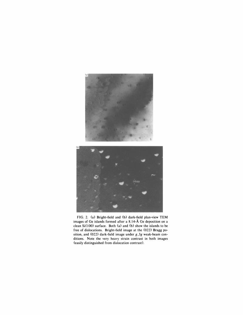
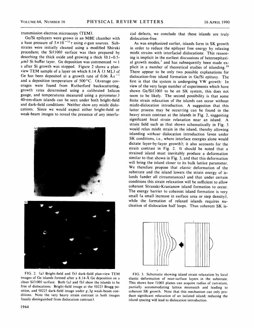
s after Si growth was stopped. Figure 2 shows a plan-view TEM sample of a layer on which 8.14 A (3 ML) ofGe has been deposited at a growth rate of 0.06 Asand a deposition temperature of 500'C. (Average cov-erages were found from Rutherford backscattering,growth rates determined using a calibrated Inficongauge, and temperatures measured using a pyrometer. )40-nm-diam islands can be seen under both bright-fieldand dark-field conditions: Neither show any misfit dislo-cations. Since we would expect either bright-field orweak-beam images to reveal the presence of any interfa-
'G'
cial defects, we conclude that these islands are trulydislocation-free.
As was emphasized earlier, islands form in SK growthin order to reduce the epilayer free energy by relaxingmisfit strains with interfacial dislocations: This reason-ing is implicit in the earliest discussions of heteroepitaxi-al growth modes, ' and has subsequently been made ex-plicit in a number of theoretical studies of islanding. '
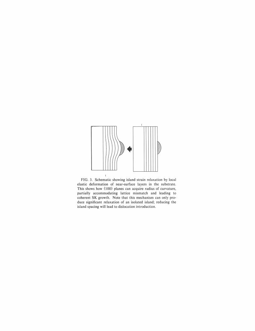
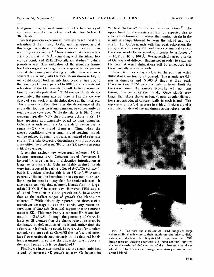
There appear to be only two possible explanations fordislocation-free island formation in Ge/Si epitaxy. Thefirst is that the system is undergoing VW growth: Inview of the very large number of experiments which haveshown Ge/Si(100) to be an SK system, this does notseem to be likely. The second possibility is that somefinite strain relaxation of the islands can occur withoutmisfit-dislocation introduction. A suggestion that thislatter process may be occurring can be found in theheavy strain contrast at the islands in Fig. 2, suggestingsignificant local strain relaxation near an island. Astrain field such as that shown schematically in Fig. 3would relax misfit strain in the island, thereby allowingislanding without dislocation introduction (even underSK conditions, i.e., where interface energies alone woulddictate layer-by-layer growth); it also accounts for thestrain contrast in Fig. 2. It should be noted that astrained island must inevitably produce a deformationsimilar to that shown in Fig. 3, and that this deformationwill bring the island closer to its bulk lattice parameter.%e therefore propose that elastic deformation of thesubstrate and the island lowers the strain energy of is-lands (under all circumstances) and that under certainconditions this strain relaxation will be sufficient to allowcoherent Stranski-Krastanow island formation to occur.The energy barrier to coherent island formation is verysmall (a small increase in surface area or step density),while the formation of relaxed islands requires nu-cleation of dislocation half loops. Thus coherent SK is-
FIG. 2. (a) Bright-field and (b) dark-field plan-view TEMimages of Ge islands formed after a 8.14-A Ge deposition on aclean Si(100) surface. Both (a) and (b) show the islands to befree of dislocations. Bright-field image at the (022) Bragg po-sition, and (022) dark-field image under g, 3g weak-beam con-ditions. Note the very heavy strain contrast in both images(easily distinguished from dislocation contrast).
I
FIG. 3. Schematic showing island strain relaxation by localelastic deformation of near-surface layers in the substrate.This shows how (100) planes can acquire radius of curvature,partially accommodating lattice mismatch and leading tocoherent SK growth. Note that this mechanism can only pro-duce significant relaxation of an isolated island; reducing theisland spacing will lead to dislocation introduction.
1944
VOLUME 64, NUMBER 16 PHYSICAL REVIEW LETTERS 16 APRIL 1990
land growth may be local minimum in the free energy ofa growing layer that has not yet nucleated true (relaxed)SK islands.
Several previous experiments have examined the strainrelaxation of thin films of Ge/Si, and it is appropriate atthis stage to address the discrepancies. Various ion-scattering experiments' ' have shown that strain relax-ation occurs at = 10 A, coinciding with the island for-mation point, and RHEED-oscillation studies' (whichprovide a very clear indication of the islanding transi-tion) also suggest a change in the in-plane lattice param-eter at the same point during growth. However, in acoherent SK island, with the local strain shown in Fig. 3,we would expect both an interface peak, arising due tothe bending of planes parallel to [0011, and a significantrelaxation of the Ge towards its bulk lattice parameter.Finally, recently published' TEM images of islands ap-proximately the same size as those in Fig. 2 show evi-
dence of a network of misfit dislocations at the interface.This apparent conflict illustrates the dependence of thestrain distributions on island densities, or equivalently ontotal average coverage. While the islands in Fig. 2 havespacings typically ) 3 && their diameter, those in Ref. 17have spacings approximately equal to their diameter.Coherent islands require substrate deformation over arange = 2X the island diameter: Thus, when thegrowth conditions give a small island spacing, islandswill be relaxed by misfit dislocations instead of substratestrain. This island-spacing dependence will thus producea transition from coherent SK to true SK growth at somecritical coverage.
It remains unclear how widespread coherent SK is-landing processes are. Coherent island formation isfavored by large barriers to dislocation introduction atlarge lattice mismatch. Coherent highly strained islandswere first reported in early studies of P-Co/Cu epitaxy,but it is unclear whether this is an SK or VW system;generally, dislocation introduction is expected at an ear-lier stage for metal epitaxy than for semiconductors. Italso seems unlikely that coherent islands form in large-misfit III-V/III-V heteroepitaxy. However, TEM studiesof island formation in GaAs growth on Si have shownthat at the earliest stages of growth the islands arecoherent. ' While this study reported the absence of amonolayer coverage outside the islands, very recent ob-servations of GaAs/Si (Ref. 22) suggest that the growthmode is SK. This may imply a coherent SK island for-mation in GaAs/Si, although the geometry of GaAs is-lands on Si dictates that the elastic relaxation must bedominated by deformation of the island, rather than thesubstrate. (It should be noted, however, that for a polar/nonpolar system such as GaAs/Si the surface and inter-face free energies depend strongly on the detailed bond-ing arrangements, so that the discussion given above in
the second paragraph is too simplified. )Finally, we have attempted to use the strain-stabilized
islands of coherent SK growth to grow Ge beyond its
"critical thickness" for dislocation introduction. Theupper limit for the strain stabilization expected due tosubstrate deformation is where the nominal strain in theisland is equipartitioned between the island and sub-strate: For Ge/Si islands with this peak relaxation, theepilayer strain is only 2%, and the experimental criticalthickness would be expected to increase by a factor of= 10, from 10 to 100 A. We accordingly grew a seriesof Ge layers of different thicknesses in order to establishthe point at which dislocations will be introduced intothese partially relaxed islands.
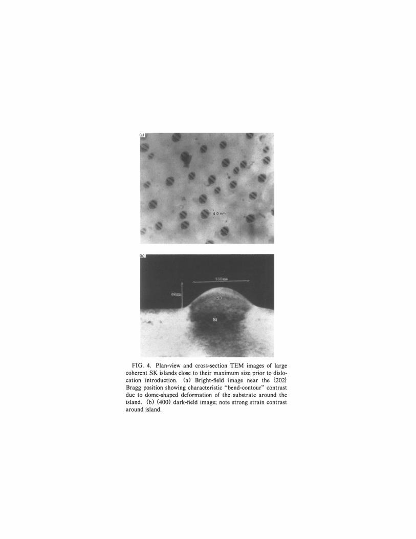
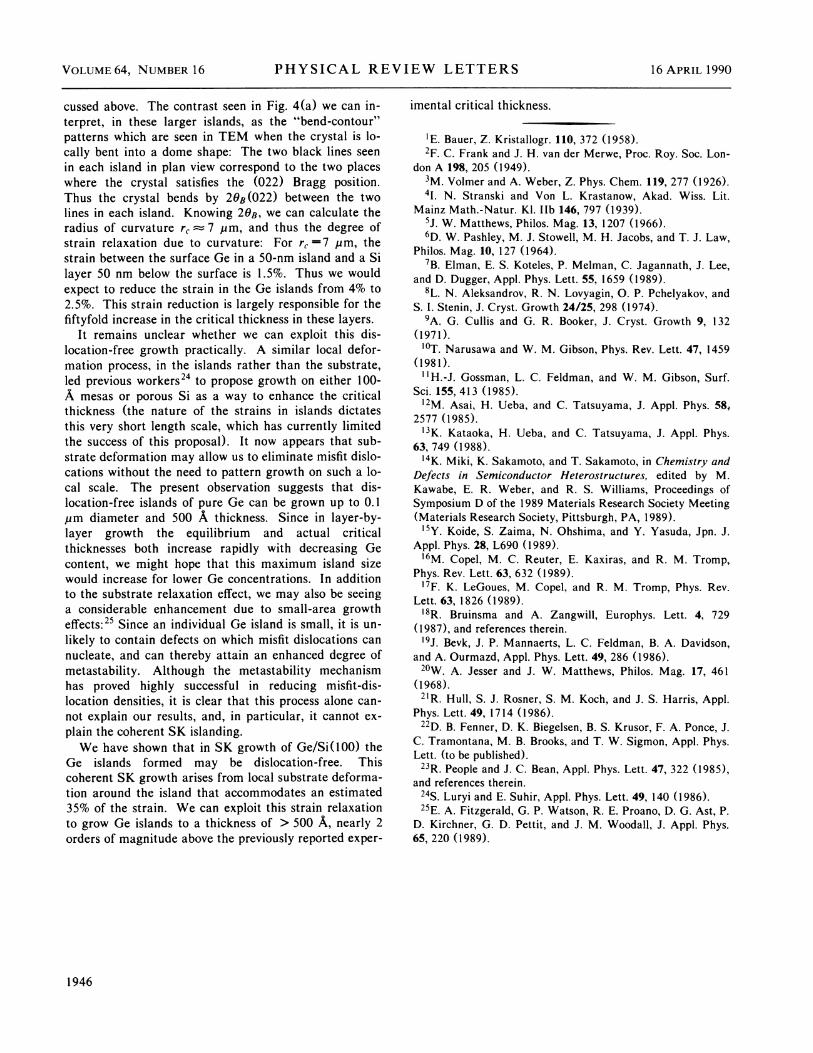
Figure 4 shows a layer close to the point at whichdislocations are finally introduced. The islands are 0.14pm in diameter and &500 A thick at their peak.(Cross-section TEM provides only a lower limit forthickness, since the sample typically will not passthrough the center of the island. ) Once islands growlarger than those shown in Fig. 4, near-circular disloca-tions are introduced concentrically in each island. Thisrepresents a fiftyfold increase in critical thickness, and issurprising in view of the maximum strain relaxation dis-
~@~a.wW .:
(b)
FIG. 4. Plan-view and cross-section TEM images of largecoherent SK islands close to their maximum size prior to dislo-cation introduction. (a) Bright-field image near the (202}Bragg position showing characteristic "bend-contour" contrastdue to dome-shaped deformation of the substrate around theisland. (b) (400) dark-field image; note strong strain contrastaround island.
1945
VOLUME 64, NUMBER 16 PHYSICAL REVIEW LETTERS 16 APRIL 1990
cussed above. The contrast seen in Fig. 4(a) we can in-
terpret, in these larger islands, as the "bend-contour"patterns which are seen in TEM when the crystal is lo-
cally bent into a dome shape: The two black lines seenin each island in plan view correspond to the two placeswhere the crystal satisfies the (022) Bragg position.Thus the crystal bends by 28tt(022) between the twolines in each island. Knowing 20q, we can calculate theradius of curvature r, = 7 pm, and thus the degree ofstrain relaxation due to curvature: For r, =7 pm, thestrain between the surface Ge in a 50-nm island and a Silayer 50 nm below the surface is 1.5%. Thus we would
expect to reduce the strain in the Ge islands from 4% to2.5%. This strain reduction is largely responsible for thefiftyfold increase in the critical thickness in these layers.
It remains unclear whether we can exploit this dis-
location-free growth practically. A similar local defor-mation process, in the islands rather than the substrate,led previous workers to propose growth on either 100-A mesas or porous Si as a way to enhance the criticalthickness (the nature of the strains in islands dictatesthis very short length scale, which has currently limited
the success of this proposal). It now appears that sub-
strate deformation may allow us to eliminate misfit dislo-cations without the need to pattern growth on such a lo-
cal scale. The present observation suggests that dis-location-free islands of pure Ge can be grown up to 0. 1
pm diameter and 500 A thickness. Since in layer-by-layer growth the equilibrium and actual criticalthicknesses both increase rapidly with decreasing Gecontent, we might hope that this maximum island sizewould increase for lower Ge concentrations. In additionto the substrate relaxation eA'ect, we may also be seeinga considerable enhancement due to small-area growtheffects: Since an individual Ge island is small, it is un-
likely to contain defects on which misfit dislocations cannucleate, and can thereby attain an enhanced degree ofmetastability. Although the metastability mechanismhas proved highly successful in reducing misfit-dis-location densities, it is clear that this process alone can-not explain our results, and, in particular, it cannot ex-plain the coherent SK islanding.
We have shown that in SK growth of Ge/Si(100) theGe islands formed may be dislocation-free. Thiscoherent SK growth arises from local substrate deforma-tion around the island that accommodates an estimated35% of the strain. %e can exploit this strain relaxationto grow Ge islands to a thickness of )500 A, nearly 2
orders of magnitude above the previously reported exper-
imental critical thickness.
'E. Bauer, Z. Kristallogr. 110, 372 (1958).2F. C. Frank and J. H. van der Merwe, Proc. Roy. Soc. Lon-
don A 198, 205 (1949).3M. Volmer and A. Weber, Z. Phys. Chem. 119, 277 (1926).4I. N. Stranski and Von L. Krastanow, Akad. Wiss. Lit.
Mainz Math. -Natur. Kl. IIb 146, 797 (1939).5J. W. Matthews, Philos. Mag. 13, 1207 (1966).D. W. Pashley, M. J. Stowell, M. H. Jacobs, and T. J. Law,
Philos. Mag. 10, 127 (1964).7B. Elman, E. S. Koteles, P. Melman, C. Jagannath, J. Lee,
and D. Dugger, Appl. Phys. Lett. 55, 1659 (1989).8L. N. Aleksandrov, R. N. Lovyagin, O. P. Pchelyakov, and
S. I. Stenin, J. Cryst. Growth 24/25, 298 (1974).A. G. Cullis and G. R. Booker, J. Cryst. Growth 9, 132
(1971).' T. Narusawa and W. M. Gibson, Phys. Rev. Lett. 47, 1459
(1981).''H. -J. Gossman, L. C. Feldman, and W. M. Gibson, Surf.
Sci. 155, 413 (1985).' M. Asai, H. Ueba, and C. Tatsuyama, J. Appl. Phys. 58,
2577 (1985).' K. Kataoka, H. Ueba, and C. Tatsuyama, J. Appl. Phys.
63, 749 (1988).' K. Miki, K. Sakamoto, and T. Sakamoto, in Chemistry and
Defects in Semiconductor Heterostructures, edited by M.Kawabe, E. R. Weber, and R. S. Williams, Proceedings ofSymposium D of the 1989 Materials Research Society Meeting(Materials Research Society, Pittsburgh, PA, 1989).
' Y. Koide, S. Zaima, N. Ohshima, and Y. Yasuda, Jpn. J.Appl. Phys. 28, L690 (1989).
' M. Copel, M. C. Reuter, E. Kaxiras, and R. M. Tromp,Phys. Rev. Lett. 63, 632 (1989).
' F. K. LeGoues, M. Copel, and R. M. Tromp, Phys. Rev.Lett. 63, 1826 (1989).
'SR. Bruinsma and A. Zangwill, Europhys. Lett. 4, 729(1987), and references therein.
' J. Bevk, J. P. Mannaerts, L. C. Feldman, B. A. Davidson,and A. Ourmazd, Appl. Phys. Lett. 49, 286 (1986).
W. A. Jesser and J. W. Matthews, Philos. Mag. 17, 461(1968).
'R. Hull, S. J. Rosner, S. M. Koch, and J. S. Harris, Appl.Phys. Lett. 49, 1714 (1986).
D. B. Fenner, D. K. Biegelsen, B. S. Krusor, F. A. Ponce, J.C. Tramontana, M. B. Brooks, and T. W. Sigmon, Appl. Phys.Lett. (to be published).
z3R. People and J. C. Bean, Appl. Phys. Lett. 47, 322 (1985),and references therein.
24S. Luryi and E. Suhir, Appl. Phys. Lett. 49, 140 (1986).25E. A. Fitzgerald, G. P. Watson, R. E. Proano, D. G. Ast, P.
D. Kirchner, G. D. Pettit, and J. M. Woodall, J. Appl. Phys.65, 220 (1989).
1946