Embed Size (px)
Citation preview
Disentangling the magnetoelectric and thermoelectric transport
in topological insulator thin films
Jinsong Zhang1, Xiao Feng
1,2, Yong Xu
3,4, Minghua Guo
1, Zuocheng Zhang
1, Yunbo Ou
2,
Yang Feng1, Kang Li
2, Haijun Zhang
3, Lili Wang
1,5, Xi Chen
1,5, Zhongxue Gan
4, Shou-
Cheng Zhang3,4
, Ke He1,5†
, Xucun Ma1,5
, Qi-Kun Xue1,5
, Yayu Wang1,5†
1State Key Laboratory of Low Dimensional Quantum Physics, Department of Physics,
Tsinghua University, Beijing 100084, P. R. China
2Institute of Physics, Chinese Academy of Sciences, Beijing 100190, P. R. China
3Department of Physics, Stanford University, Stanford, CA 94305–4045, USA
4ENN Intelligent Energy Group, ENN Science Park, Langfang, Hebei 065001, China
5Collaborative Innovation Center of Quantum Matter, Beijing 100084, China
†Emails: [email protected]; [email protected]
We report transport studies on (Bi1−xSbx)2Te3 topological insulator thin films with
tunable electronic band structure. We find a doping and temperature regime in which the
Hall coefficient is negative indicative of electron-type carriers, whereas the Seebeck
coefficient is positive indicative of hole-type carriers. This sign anomaly is due to the
distinct transport behaviors of the bulk and surface states: the surface Dirac fermions
dominate magnetoelectric transport while the thermoelectric effect is mainly determined
by the bulk states. These findings may inspire new ideas for designing topological
insulator-based high efficiency thermoelectric devices.
I. INTRODUCTION
Thermoelectric power generation and refrigeration utilize the conversion between
heat and electricity carried by electrons in solids, and thus have the advantages of being
quiet, reliable, flexible, and eco-friendly [1-4]. The main hurdle for the widespread
application of thermoelectricity is its low efficiency compared to conventional
technologies. The performance of thermoelectric devices is evaluated by a dimensionless
figure of merit defined as ZT = S2T/, where S, , T, and are the Seebeck coefficient,
electrical conductivity, absolute temperature, and thermal conductivity, respectively.
Despite extensive efforts in the past few decades, the maximum room-temperature ZT for
commercial thermoelectric materials has remained at ~ 1 [3-6]. In recent years, many
novel ideas for improving the thermoelectric efficiency have been proposed [3]. A
particularly attractive proposal is to improve ZT through nanostructuring, which modifies
the electronic structure by quantum size effect and reduces the thermal conductivity by
boundary scatterings [2,7]. This idea has inspired continuing experimental efforts to
search for the proof-of-principle devices consisting of nanocomposites [6,8], nanowires
[9] and superlattices [10,11].
Very recently, Bi2Te3 and Sb2Te3, known for decades as the best room-temperature
thermoelectric materials, were discovered to be topological insulators (TIs) [12-14]. The
topological surface states (SSs) enclosing the TIs provide new opportunity for enhancing
their thermoelectric efficiency, because the additional surface transport channel may help
circumvent the problems of a single channel where various transport parameters are all
entangled and thus cannot be manipulated separately. There have been numerous
theoretical discussions on the effect of topological SSs on the thermoelectric behavior of
TIs [15-22]. It has been argued that the topological protection of the SSs leads to superb
electrical conductivity [16], thus may give a further boost to ZT. On the downside, the
Dirac-like linear dispersion of the SSs is not optimal for the Seebeck coefficient, which
prefers a sharp change of electron density of state (DOS) near the Fermi level (EF) [23].
There are further complications and meanwhile opportunities caused by the interplay
between the surface and bulk states [17], as well as the top and bottom SSs themselves
[16,24]. In particular, a recent theoretical work shows that topological SSs can
dramatically enhance ZT when the EF is tuned close to the bottom of the bulk conduction
band or top of the bulk valence band [17]. In this case, the life-times for quasi-particle
excitations above and below the EF are strongly asymmetrical, leading to opposite sign
for the Seebeck and Hall coefficients.
At the current stage, most of these issues have not been investigated adequately by
experiments. In this paper we report transport studies on molecular beam epitaxy (MBE)-
grown (Bi1−xSbx)2Te3 TI thin films with tunable band structure by varying the Bi/Sb ratio
[25]. We find a doping and temperature regime in which the Hall coefficient is negative
indicative of electron-type carriers, whereas the Seebeck coefficient is positive indicative
of hole-type carriers. This sign anomaly is due to distinct transport behaviors of the bulk
and surface states: the surface Dirac fermions dominate magnetoelectric transport while
the thermoelectric effect is mainly determined by the bulk states. These findings may
inspire new ideas designing TI-based high efficiency thermoelectric devices.
II. METHODOLOGY
A. MBE sample growth
The (Bi1−xSbx)2Te3 thin films are grown on insulating SrTiO3 substrates (2 mm 8
mm 0.25 mm) by using the same growth method described in our previous report [25].
All the samples have the same thickness d = 5 quintuple layers (QLs). Before sample
growth, the substrates are degassed at 550 °C for 10 min and then heated at 650 °C for 25
min in the ultrahigh vacuum chamber. To reduce Te vacancies, the growth is kept in Te-
rich condition with the substrate temperature at 200 °C. Finally, an amorphous Te layer
(~10 nm) is deposited on the top to prevent unintentional contamination from ambience.
B. Transport measurements
Figure 1(a) shows the schematic setup of the transport measurements on the TI
films. Electrical transport properties including resistance and the Hall effect are measured
in an isothermal condition. Thermoelectric measurements are carried out in high-vacuum
condition with the pressure lower than 110-6
mbar. A thin-film heater is mounted on the
right end of the substrate to produce the temperature gradient. A pair of fine-gauge
thermocouples (type E, CHROMEGA®/Constantan) are connected in subtractive series
and thermally anchored to the substrate to monitor the temperature difference. The DC
voltages of the Seebeck effect (or the thermopower) and thermocouples are recorded by
nano-voltmeters (Keithley 2002 multimeter with 1801 preamplifier), and the Seebeck
coefficient of the gold leads for thermoelectric measurement is subtracted.
C. Theoretical calculations
To carry out ab initio calculations of the TI band structure, the BSTATE package
[26] with the plane-wave pseudo-potential is employed in the framework of the Perdew–
Burke–Ernzerhof-type exchange-correlation functional [27] with generalized gradient
approximation of the density functional theory. The kinetic energy cutoff is fixed to 340
eV, and a k-mesh is taken as 8×8×1 for the 5 QL free-standing slab with a 25 Bohr
vacuum layer. Virtual crystal method [28] is used to simulate the mixing of Bi and Sb.
The lattice constant and the atomic position are obtained by linearly interpolating
between Bi2Te3 and Sb2Te3. The Seebeck coefficient as a function of temperature and
Fermi level is calculated by the Landauer transport approach with the constant mean free
path model [29] based on the band structure in a dense k-mesh 400×400×1 from the
maximally localized Wannier functions [30].
III. EXPERIMENTAL RESULTS
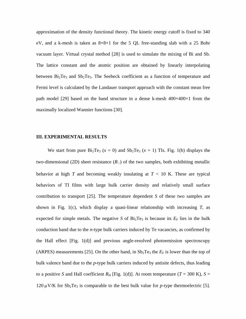
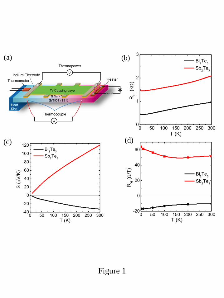
We start from pure Bi2Te3 (x = 0) and Sb2Te3 (x = 1) TIs. Fig. 1(b) displays the
two-dimensional (2D) sheet resistance (R□) of the two samples, both exhibiting metallic
behavior at high T and becoming weakly insulating at T < 10 K. These are typical
behaviors of TI films with large bulk carrier density and relatively small surface
contribution to transport [25]. The temperature dependent S of these two samples are
shown in Fig. 1(c), which display a quasi-linear relationship with increasing T, as
expected for simple metals. The negative S of Bi2Te3 is because its EF lies in the bulk
conduction band due to the n-type bulk carriers induced by Te vacancies, as confirmed by
the Hall effect [Fig. 1(d)] and previous angle-resolved photoemission spectroscopy
(ARPES) measurements [25]. On the other hand, in Sb2Te3 the EF is lower than the top of
bulk valence band due to the p-type bulk carriers induced by antisite defects, thus leading
to a positive S and Hall coefficient RH [Fig. 1(d)]. At room temperature (T = 300 K), S =
120V/K for Sb2Te3 is comparable to the best bulk value for p-type thermoelectric [5].
While for Bi2Te3 the amplitude of S is only about 30 V/K, much lower than that for the
best n-type bulk thermoelectric [5]. This can be understood based on the Drude model for
free electron gas, in which the Seebeck coefficient is expressed as
=
. (1)
A large carrier density, hence a large EF, could significantly reduce S. Indeed, for our
Bi2Te3 film the nominal carrier density estimated from the Hall coefficient is n3D = 1/eRH
= 1.21020
cm-3
at 300 K, which is much larger than the optimal carrier density (~ 21019
cm-3
) for bulk thermoelectric [5].
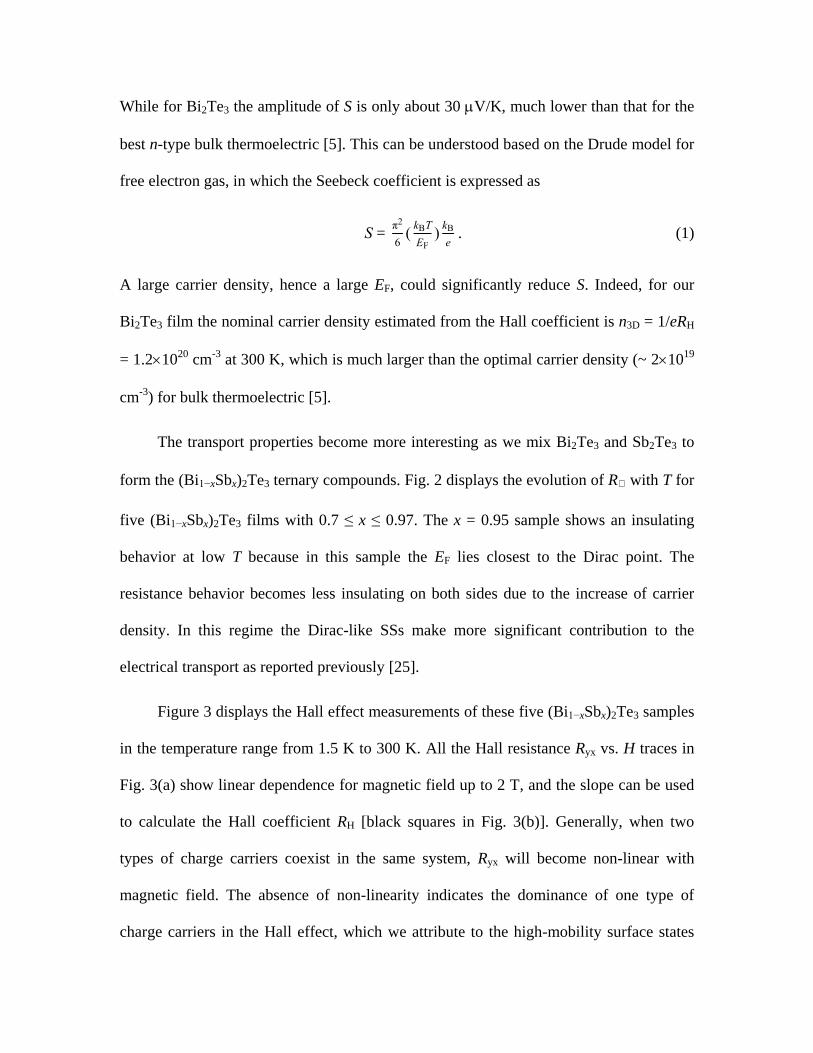
The transport properties become more interesting as we mix Bi2Te3 and Sb2Te3 to
form the (Bi1−xSbx)2Te3 ternary compounds. Fig. 2 displays the evolution of R□ with T for
five (Bi1−xSbx)2Te3 films with 0.7 ≤ x ≤ 0.97. The x = 0.95 sample shows an insulating
behavior at low T because in this sample the EF lies closest to the Dirac point. The
resistance behavior becomes less insulating on both sides due to the increase of carrier
density. In this regime the Dirac-like SSs make more significant contribution to the
electrical transport as reported previously [25].
Figure 3 displays the Hall effect measurements of these five (Bi1−xSbx)2Te3 samples
in the temperature range from 1.5 K to 300 K. All the Hall resistance Ryx vs. H traces in
Fig. 3(a) show linear dependence for magnetic field up to 2 T, and the slope can be used
to calculate the Hall coefficient RH [black squares in Fig. 3(b)]. Generally, when two
types of charge carriers coexist in the same system, Ryx will become non-linear with
magnetic field. The absence of non-linearity indicates the dominance of one type of
charge carriers in the Hall effect, which we attribute to the high-mobility surface states
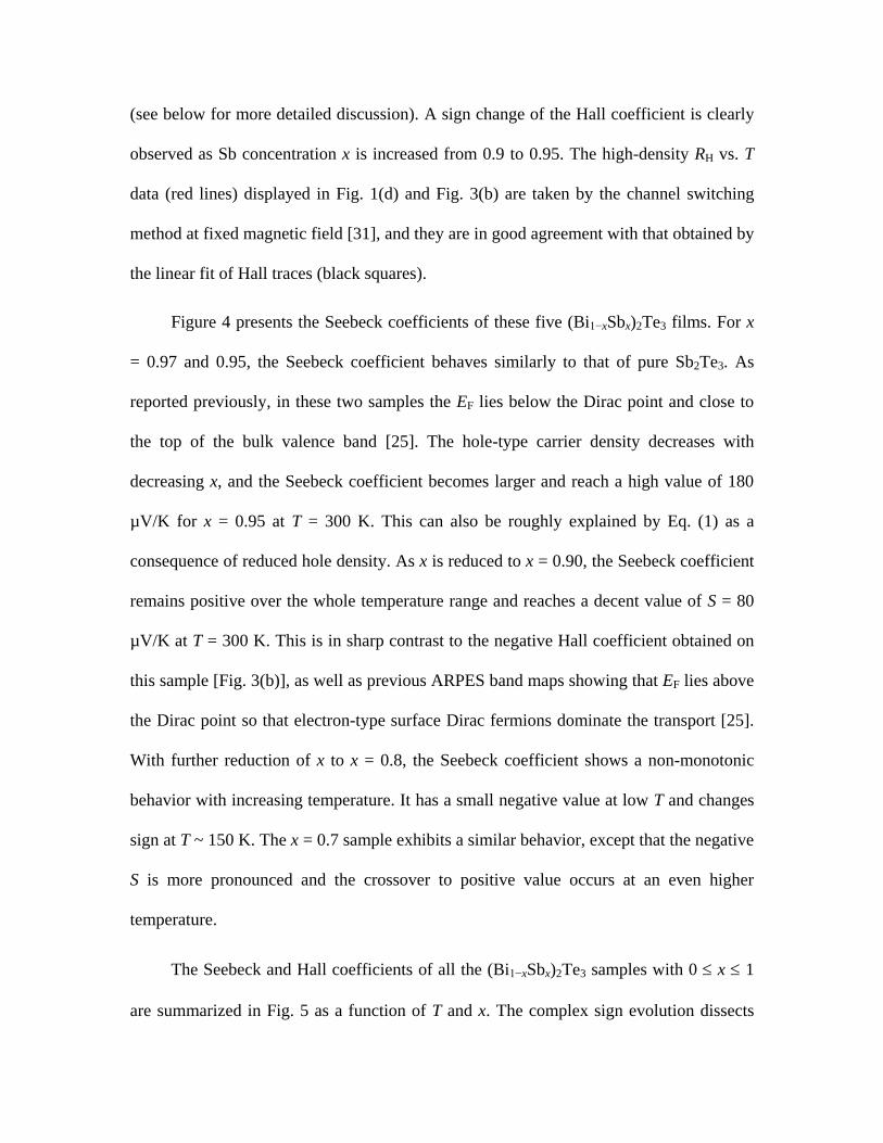
(see below for more detailed discussion). A sign change of the Hall coefficient is clearly
observed as Sb concentration x is increased from 0.9 to 0.95. The high-density RH vs. T
data (red lines) displayed in Fig. 1(d) and Fig. 3(b) are taken by the channel switching
method at fixed magnetic field [31], and they are in good agreement with that obtained by
the linear fit of Hall traces (black squares).
Figure 4 presents the Seebeck coefficients of these five (Bi1−xSbx)2Te3 films. For x
= 0.97 and 0.95, the Seebeck coefficient behaves similarly to that of pure Sb2Te3. As
reported previously, in these two samples the EF lies below the Dirac point and close to
the top of the bulk valence band [25]. The hole-type carrier density decreases with
decreasing x, and the Seebeck coefficient becomes larger and reach a high value of 180
µV/K for x = 0.95 at T = 300 K. This can also be roughly explained by Eq. (1) as a
consequence of reduced hole density. As x is reduced to x = 0.90, the Seebeck coefficient
remains positive over the whole temperature range and reaches a decent value of S = 80
µV/K at T = 300 K. This is in sharp contrast to the negative Hall coefficient obtained on
this sample [Fig. 3(b)], as well as previous ARPES band maps showing that EF lies above
the Dirac point so that electron-type surface Dirac fermions dominate the transport [25].
With further reduction of x to x = 0.8, the Seebeck coefficient shows a non-monotonic
behavior with increasing temperature. It has a small negative value at low T and changes
sign at T ~ 150 K. The x = 0.7 sample exhibits a similar behavior, except that the negative
S is more pronounced and the crossover to positive value occurs at an even higher
temperature.
The Seebeck and Hall coefficients of all the (Bi1−xSbx)2Te3 samples with 0 x 1
are summarized in Fig. 5 as a function of T and x. The complex sign evolution dissects
the phase diagram into three distinct regions: negative S with negative RH (region I),
positive S with negative RH (region II), and positive S with positive RH (region III). In
most materials the sign of S is consistent with the type of charge carriers estimated from
the Hall effect [5,32,33]. In other words, if the sign of S changes at a critical doping or
temperature [34], the Hall coefficient is expected to reverse sign simultaneously.
However, in the (Bi1−xSbx)2Te3 TI films studied here, the sign consistency between the
Seebeck coefficient and Hall coefficient is violated in certain region of the phase diagram.
IV. THEORETICAL DISCUSSIONS
To understand the anomalous transport properties of the (Bi1−xSbx)2Te3 films, we
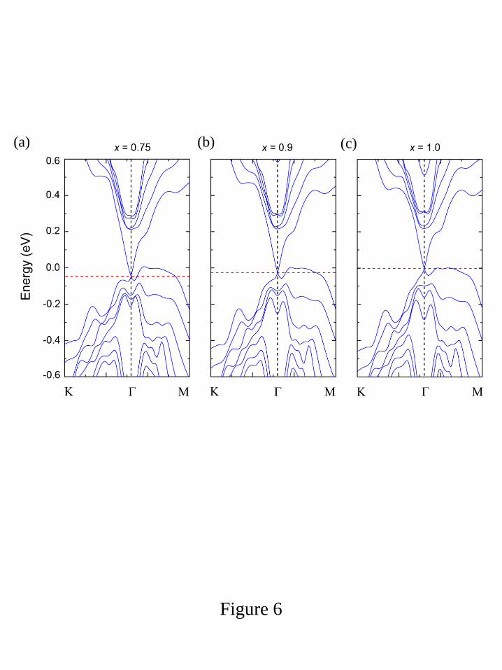
have performed first principle electronic structure calculations. Fig. 6 shows the
calculated band structures of 5 QL (Bi1−xSbx)2Te3 films along the K M direction for
x = 0.75, 0.90 and 1.0. The surface states can be clearly identified by two linear bands
crossing at the point. For 0.75 ≤ x ≤ 1.0, the overall band structures are almost the same
and the only differences happen at the relative positions between the Dirac point and the
bulk VBM along the M direction. Therefore, it is reasonable to calculate the
thermoelectric properties of various (Bi1−xSbx)2Te3 samples by tuning the EF for different
doping levels based on the band structure for x = 0.90.
The transport coefficients are calculated by the Landauer approach, in which the
Seebeck coefficient S is described as B 1 0( / )( / )S k e I I . Here kB is the Boltzmann
constant, e is the elementary charge, and In (n = 0, 1) is the dimensionless integrals given
by 2
( )( 1)
n x
n x
x eI dx x
e
T , in which F B( ) / ( )x E E k T and ( ) ( )x ET T is the
electronic transmission function. ( ) ( ) ( )E M E ET T . M(E) is the distribution of
conduction modes, which counts the number of conduction channels at a given energy E
and is proportional to the group velocity along the transport direction times the density of
states. Fig. 7 shows the M(E) for the 5 QL (Bi1−xSbx)2Te3 film with x = 0.9 obtained by
directly counting the conduction channels over the whole Brillouin zone. ( )ET is the
transmission probability, which for diffusive transport is given by ( ) ( ) /E E LT ,
where ( )E represents the mean free path and L is the transport length. ( )ET is usually
calculated using the approximation of constant scattering time or constant mean free path
[35]. However, a dual scattering time model is necessary for TIs [17] because the
topological surface states are protected from backscattering and thus have longer
scattering time than the bulk states. Here we use 1( )E for surface states with energies
within the bulk gap and 2( )E otherwise. The ratio 1 2/r is the only variable
relevant to S, and should be larger than 1 to account for the topological protection of
surface states. To reproduce the experimental S for x = 0.9 at 300 K, r = 5 is selected.
Notice that r in reality is sample-dependent and might be different. However, according
to our tests, this would not influence the calculated S qualitatively, and thus would not
affect our theoretical discussion that is kept at a qualitative level.
To understand the sign anomaly between the Seebeck and Hall coefficients, we
calculate the Seebeck coefficient as a function of T based on the band structure for x = 0.9
and vary the EF to mimic the influence of x in experiment [23], as presented in Fig. 8. For
EF below the bulk VBM (i.e., EF ≤ 0), S is always positive and increases with increasing
EF. In contrast, for EF > 0 increasing EF leads to a downward shift and sign reversal of S
from positive to negative at low temperatures. The critical point TC, where the sign
change happens, gets higher for increasing EF. All these features are qualitatively
consistent with the experimental observations.
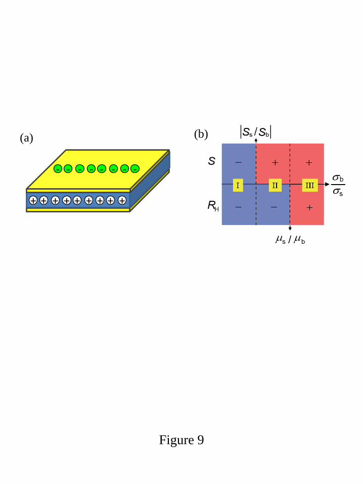
The underlying physical picture of the unexpected transport behavior of TIs can be
illustrated intuitively by involving the contributions from both the surface and bulk states,
as shown in Fig. 9(a). Specifically, the Seebeck coefficient can be expressed as:
S = (σsSs + σbSb)/(σs + σb). (2)
Here σs,b and Ss,b represent the electrical conductivity and Seebeck coefficient of the
surface and bulk states, respectively. We focus on the regime of EF above (and close to)
the bulk VBM, where the interesting sign change of S happens. In this regime Ss is
negative because the Dirac point is located below EF, whereas Sb is always positive due to
the thermally activated hole-type bulk carriers. Their relative contribution to the total S is
controlled by the ratio σb/σs, which depends sensitively on T and EF. Specifically,
decreasing T and/or increasing EF (decreasing x in experiments) would reduce σb/σs
because of the reduction of bulk carrier density. At a critical T or x, the sign of S will
change from positive to negative, which is precisely the trend observed in experiment
(see Fig. 5).
From Eq. (2) it is clear that the critical condition for changing the sign of S is σb/σs
= |Ss/Sb| provided that Ss and Sb have opposite signs. What about the Hall coefficient RH?
In the presence of both surface and bulk conduction, RH can be derived from the two-
band model as RH = (σsµs + σbµb)/(σs + σb)2, where µs,b represents the carrier mobility.
The sign of RH is reversed when σb/σs = µs/µb. Interestingly, the critical conditions for
changing the sign of S and RH differ considerably in TI due to the unique properties of the
Dirac-like SSs. The linear dispersion indicates weak electron-hole asymmetry around EF,
which leads to much smaller Ss than Sb so that |Ss/Sb| ≪ 1 is easily satisfied. On the other
hand, topological protection of the surface Dirac fermions strongly enhances its mobility
[16], resulting in µs/µb ≫ 1 as evidenced by previous experiment [36]. Therefore, there
exists a sizeable region (region II in Fig. 5) in which the relationship |Ss/Sb| < σb/σs < µs/µb
is valid, causing the opposite sign of S and RH. In region I or III, the ratio σb/σs is too
small or too large such that either the surface or bulk states dominate both types of
transports, giving the same sign for S and RH. Fig. 9(b) summarizes the theoretical phase
diagram, which qualitatively reproduces the experimental one in Fig. 5 given the fact that
in the experiments increasing T and x enhances σb/σs.
V. CONCLUSION
To conclude, we observe a sign anomaly between the Seebeck and Hall coefficients
in 5 QL (Bi1−xSbx)2Te3 TI thin films over a range of Sb concentrations and temperatures.
The origin is that p-type bulk states dominate the thermoelectric transport, whereas n-
type SSs dominate the magnetoelectric transport. Our experiment establishes the
importance of topological SSs in the thermoelectric effect of TI, which has been
frequently emphasized in theoretical proposals [15-22]. Unlike the common two-band
scenario, the surface and bulk channels of TI are separated in space, which enables the
design of high-efficiency thermoelectric devices through novel heterojunction and
superlattice architectures. The basic philosophy is to control the surface and bulk bands
separately and take advantage of the optimal transport properties of each channel to
further enhance ZT [20]. Moreover, the interactions between the surface and bulk states
provides a new knob for improving ZT. It has been proposed recently that the surface-
bulk coupling will lead to a strongly energy dependent lifetime for the SSs [17], which
causes a maximum of Ss and a significantly enhanced ZT. In this work our TI films are
quite far away from the situation considered in the theory in Ref. 17. For future
investigations we plan to tune the system into a regime dominated by the topological SSs
to test these theoretical proposals.
Jinsong Zhang, Xiao Feng and Yong Xu contributed equally to this work. We
acknowledge Wenhui Duan and Xiaobin Chen for suggestions and comments. This work
was supported by the National Natural Science Foundation of China, the Ministry of
Science and Technology of China and the Chinese Academy of Sciences.
References
[1] L. E. Bell, Science 321, 1457 (2008).
[2] M. S. Dresselhaus, G. Chen, M. Y. Tang, R. G. Yang, H. Lee, D. Z. Wang, Z. F. Ren, J. P.
Fleurial, and P. Gogna, Adv Mater 19, 1043 (2007).
[3] G. J. Snyder and E. S. Toberer, Nat Mater 7, 105 (2008).
[4] F. J. DiSalvo, Science 285, 703 (1999).
[5] H. Scherrer and S. Scherrer, in CRC Handbook of Thermoelectrics, edited by D. M. Rowe
(CRC Press, Boca Raton, 1995).
[6] B. Poudel et al., Science 320, 634 (2008).
[7] L. D. Hicks and M. S. Dresselhaus, Phys Rev B 47, 12727 (1993).
[8] K. Biswas, J. He, I. D. Blum, C.-I. Wu, T. P. Hogan, D. N. Seidman, V. P. Dravid, and M.
G. Kanatzidis, Nature 489, 414 (2012).
[9] A. I. Boukai, Y. Bunimovich, J. Tahir-Kheli, J.-K. Yu, W. A. Goddard Iii, and J. R. Heath,
Nature 451, 168 (2008).
[10] R. Venkatasubramanian, E. Siivola, T. Colpitts, and B. O'Quinn, Nature 413, 597 (2001).
[11] T. C. Harman, P. J. Taylor, M. P. Walsh, and B. E. LaForge, Science 297, 2229 (2002).
[12] H. Zhang, C.-X. Liu, X.-L. Qi, X. Dai, Z. Fang, and S.-C. Zhang, Nat Phys 5, 438 (2009).
[13] Y. L. Chen et al., Science 325, 178 (2009).
[14] Y. Xia et al., Nat Phys 5, 398 (2009).
[15] R. Takahashi and S. Murakami, Phys Rev B 81, 161302 (2010).
[16] P. Ghaemi, R. S. K. Mong, and J. E. Moore, Phys Rev Lett 105, 166603 (2010).
[17] Y. Xu, Z. Gan, and S.-C. Zhang, Phys Rev Lett 112, 226801 (2014).
[18] O. A. Tretiakov, A. Abanov, and J. Sinova, Appl Phys Lett 99, 113110 (2011).
[19] L. Müchler, F. Casper, B. Yan, S. Chadov, and C. Felser, Phys Status Solidi-R 7, 91
(2013).
[20] H. Osterhage, J. Gooth, B. Hamdou, P. Gwozdz, R. Zierold, and K. Nielsch, Appl Phys
Lett 105, 123117 (2014).
[21] R. Takahashi and S. Murakami, Semicond Sci Tech 27, 124005 (2012).
[22] O. A. Tretiakov, A. Abanov, and J. Sinova, J Appl Phys 111, 07E319 (2012).
[23] J. P. Heremans, V. Jovovic, E. S. Toberer, A. Saramat, K. Kurosaki, A. Charoenphakdee,
S. Yamanaka, and G. J. Snyder, Science 321, 554 (2008).
[24] Y. Zhang et al., Nat Phys 6, 584 (2010).
[25] J. Zhang et al., Nat Commun 2, 574 (2011).
[26] Z. Fang and K. Terakura, J Phys Condens Matter 14, 3001 (2002).
[27] J. P. Perdew, K. Burke, and M. Ernzerhof, Phys Rev Lett 77, 3865 (1996).
[28] L. Bellaiche and D. Vanderbilt, Phys Rev B 61, 7877 (2000).
[29] J. Maassen and M. Lundstrom, Appl Phys Lett 102 (2013).
[30] N. Marzari and D. Vanderbilt, Phys Rev B 56, 12847 (1997).
[31] H. H. Sample, W. J. Bruno, S. B. Sample, and E. K. Sichel, J Appl Phys 61, 1079 (1987).
[32] C. B. Satterthwaite and R. W. Ure, Phys Rev 108, 1164 (1957).
[33] A. Boulouz, S. Chakraborty, A. Giani, F. P. Delannoy, A. Boyer, and J. Schumann, J Appl
Phys 89, 5009 (2001).
[34] Y. S. Hor, D. Qu, N. P. Ong, and R. J. Cava, J Phys Condens Matter 22 (2010).
[35] R. Kim, S. Datta, and M. S. Lundstrom, J Appl Phys 105 (2009).
[36] D.-X. Qu, Y. S. Hor, J. Xiong, R. J. Cava, and N. P. Ong, Science 329, 821 (2010).
Figure captions
FIG. 1 (color online). Schematic diagram for transport measurements and the results of 5
QL Bi2Te3 and Sb2Te3 films. (a) Schematic device for the thermoelectric measurements.
(b) The sheet resistance (R□) of Bi2Te3 and Sb2Te3 shows metallic behavior at high T and
turns to weakly insulating at low T. (c) In Bi2Te3 and Sb2Te3 the Sxx has a quasi-linear T
dependence, but with opposite signs. (d) The Hall coefficient of Bi2Te3 is negative,
indicating electron-like charge carriers which contribute negative S; whereas in Sb2Te3
the hole-like charge carriers contribute positive S. The solid symbols are obtained by
fitting the slope of field dependent Hall traces at fixed temperatures, and the lines are
measured by switching the current and voltage contacts at fixed magnetic field when the
temperature is slowly swept [31].
FIG. 2 (color online). The temperature dependence of the sheet resistance for the 5 QL
(Bi1−xSbx)2Te3 films with 0.7 ≤ x ≤ 0.97. R□ shows an enhanced insulating tendency when
x is close to 0.95.
FIG. 3 (color online). The Hall effect for the 5 QL (Bi1−xSbx)2Te3 films with 0.7 ≤ x ≤
0.97. (a) Field dependence of the Hall resistance measured at constant temperatures. (b)
The Hall coefficient RH as a function of continuously increased (red lines) and constant
(black squares) temperatures. For each sample the sign of RH is unchanged with
increasing T (negative for x ≤ 0.9 and positive for x 0.95).
FIG. 4 (color online). The Seebeck coefficient for the 5 QL (Bi1−xSbx)2Te3 films with 0.7
≤ x ≤ 0.97. In samples with x = 0.7 and 0.8, a sign reversal of S from negative to positive
is revealed as T rises. As x is further increased from x = 0.9 to 0.97, the sign reversal
totally disappears and a maximum positive value is found with x = 0.95. At high T, the
sign anomaly between S and RH is clearly revealed for 0.7 ≤ x ≤ 0.9.
FIG. 5 (color online). The phase diagram of (Bi1−xSbx)2Te3 films summarizing the Sxx as a
function of x and T. The contours with S = 0 (wine dash line) and RH = 0 (blue dash-dot
line) divide this phase diagram into three regions: negative Sxx and RH (region I), positive
Sxx but negative RH (region II), and positive S and RH (region III).
FIG. 6 (color online). The band structure of 5 QL (Bi1−xSbx)2Te3 calculated by the density
functional theory with x = 0.75 (a), 0.9 (b), and 1.0 (c). Red dashed lines indicate the
position of Dirac point, and black dashed lines represent the locations of the points.
The bulk VBM is selected as the energy reference (E = 0).
FIG. 7 (color online). The calculated distribution of conduction modes M(E) as a function
of energy for the 5 QL (Bi1−xSbx)2Te3 film with x = 0.9.
FIG. 8 (color online). The Seebeck coefficient as a function T and EF calculated based on
the band structure in Fig. 6(b). While Sxx is always positive for EF ≤ 0, Sxx changes from
negative to positive with increasing T for EF > 0.
FIG. 9 (color online). (a) Schematic drawing shows the coexistence of electron-type
surface Dirac fermions and hole-type bulk carriers in a TI thin film. (b) A theoretical
phase diagram for TI thin films with n-type surface and p-type bulk charge carriers.
When increasing σb/σs (realized by increasing T and Sb content in experiment), a
negative-to-positive sign change happens for both S and RH but at distinctly different
conditions: σb/σs = |Ss/Sb| ≪ 1 for S and σb/σs = µs/µb ≫ 1 for RH. Three different regions
(I/II/III) are defined according to the signs of S and RH, the same as in Fig. 5.
0 50 100 150 200 250 300-40
-20
0
20
40
60
80
100
120
S (V
/K)
T (K)
Bi2Te
3
Sb2Te
3
0 50 100 150 200 250 300-20
0
20
40
60
RH (
/T)
T (K)
Bi2Te
3
Sb2Te
3
(a)
0 50 100 150 200 250 3000
1
2
3
Bi2Te
3
Sb2Te
3
Rsq (
k
)T (K)
(d) (c)
(b)
Figure 1
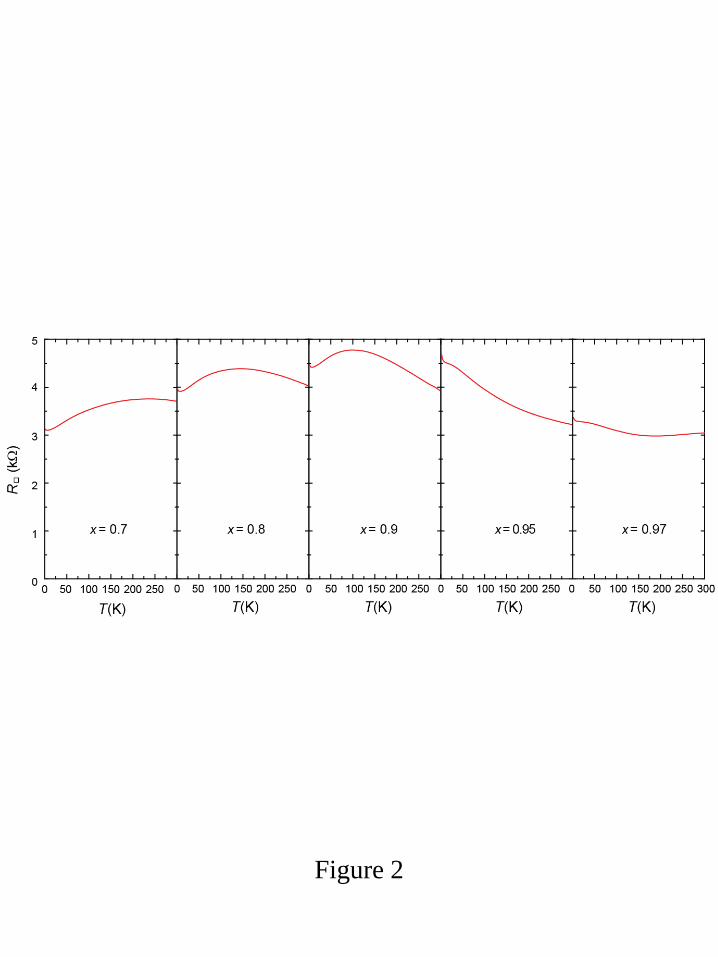
Figure 2
Figure 3
(a)
(b)
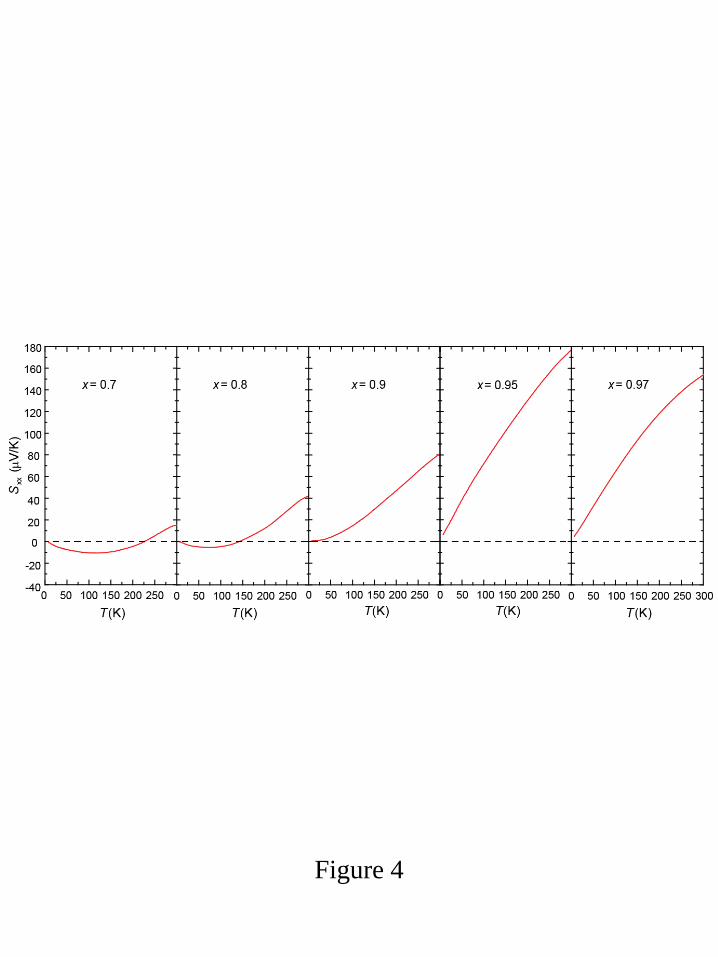
Figure 4
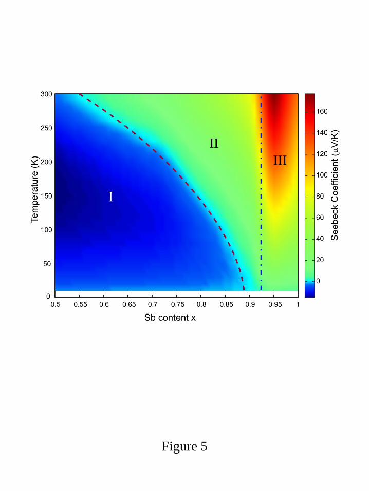
Figure 5
(a) (b) (c)
Figure 6
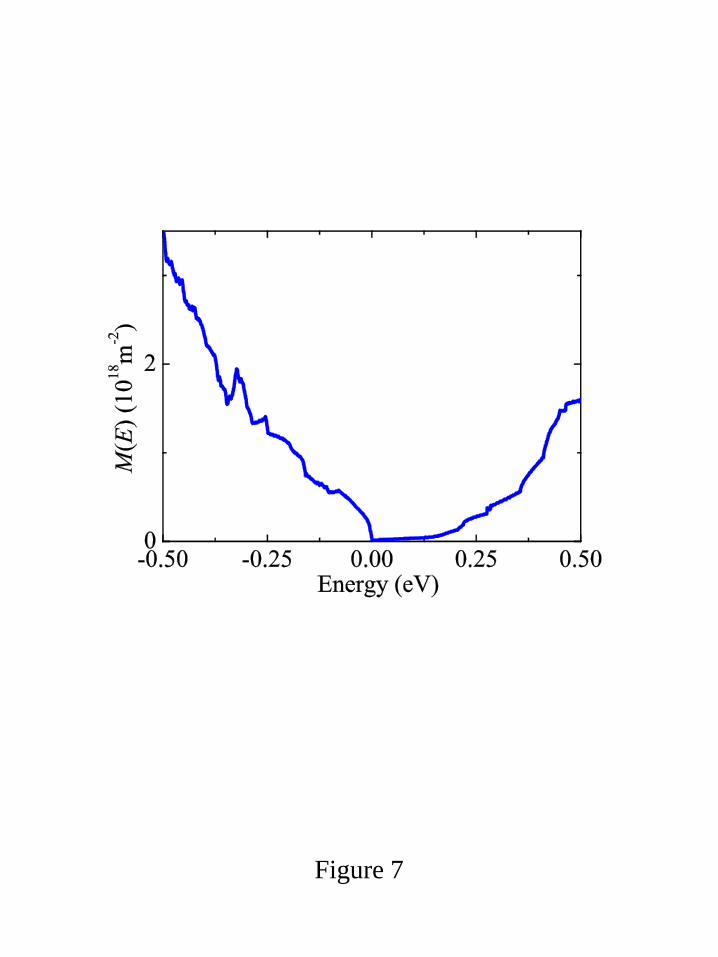
Figure 7
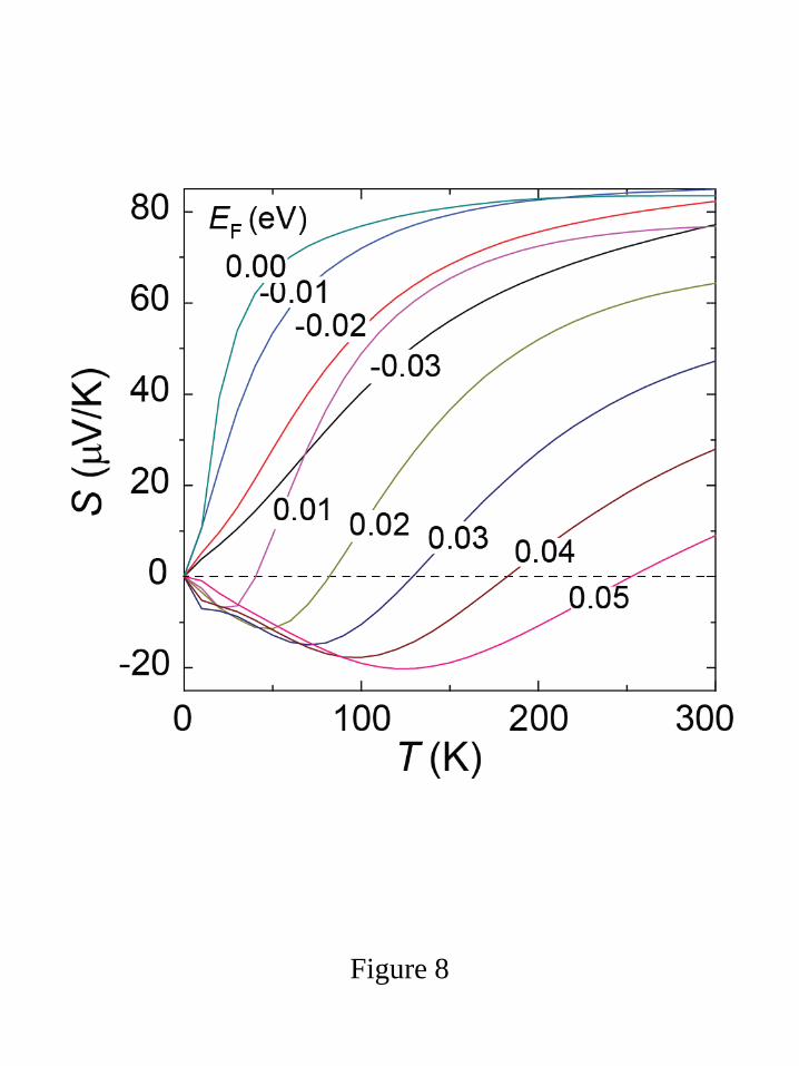
Figure 8
d c
+ + + + + + + + +
- - - - - - - -
Figure 9
(b) (a)


![Electromagnetic-Magnetoelectric Duality for Waveguides · 2015. 10. 23. · arXiv:1510.06458v1 [physics.optics] 21 Oct 2015 Electromagnetic-Magnetoelectric Duality for Waveguides](https://img.pdfslide.us/doc/110x75/6025080042b59e610d00e805/electromagnetic-magnetoelectric-duality-for-waveguides-2015-10-23-arxiv151006458v1.jpg)