Embed Size (px)
Citation preview

Directives & Memory Space & Stack Overview
Dr. Farid Farahmand Updated: 2/18/2014
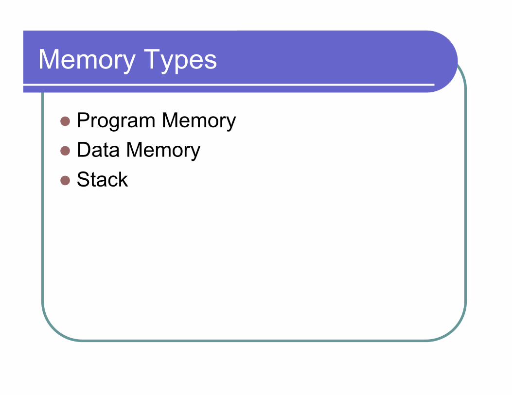
Memory Types
l Program Memory l Data Memory l Stack
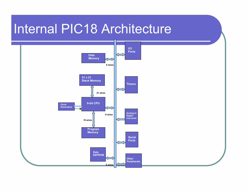
8-bit CPU
Program Memory
Data Memory
Clock Generation
I/O Ports
Timers
Analog to Digital Converter
Serial Ports
Other Peripherals
16 wires
8 wires
Data EEPROM
31 x 21 Stack Memory
21 wires
8 wires
8 wires
Internal PIC18 Architecture
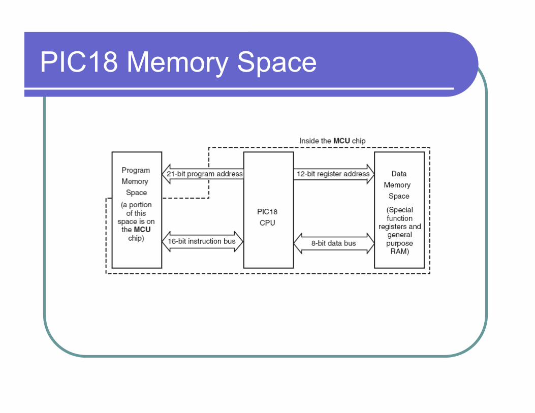
PIC18 Memory Space
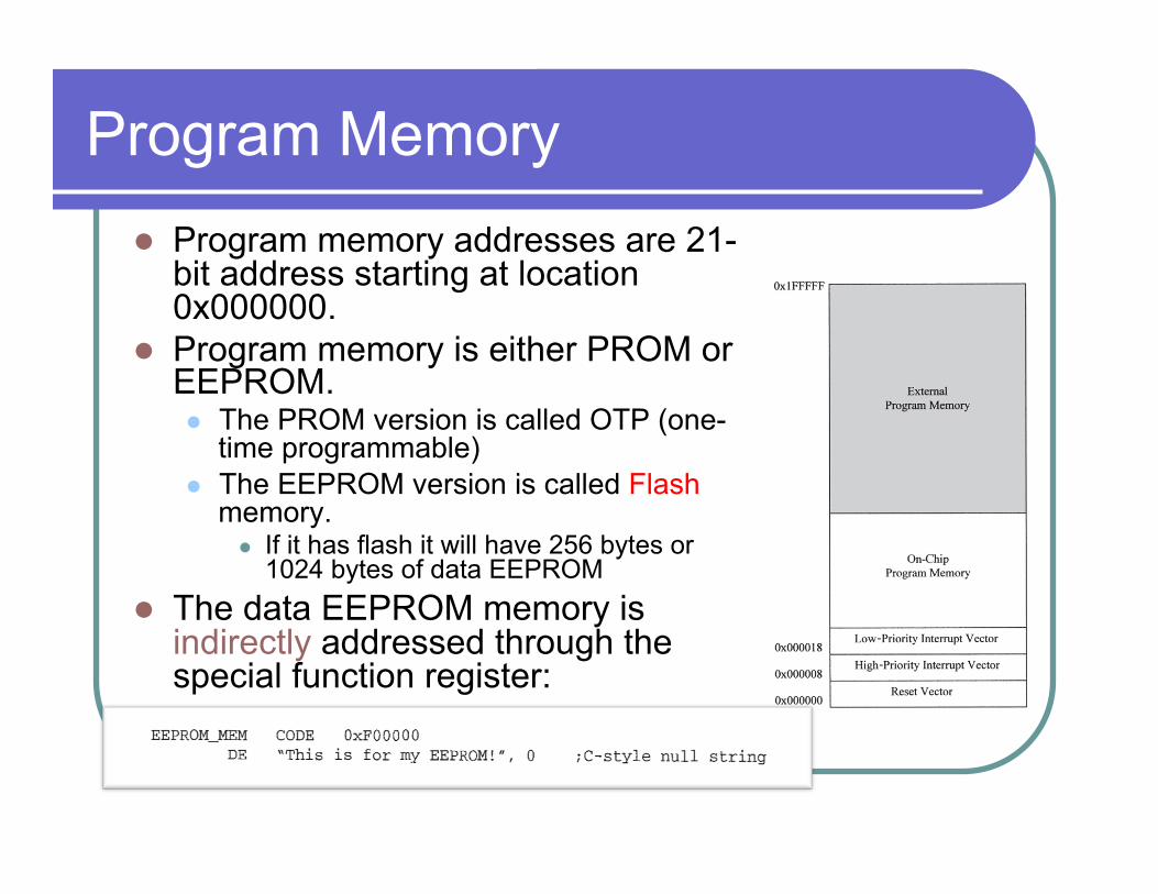
Program Memory l Program memory addresses are 21-
bit address starting at location 0x000000.
l Program memory is either PROM or EEPROM. l The PROM version is called OTP (one-
time programmable) l The EEPROM version is called Flash
memory. l If it has flash it will have 256 bytes or
1024 bytes of data EEPROM l The data EEPROM memory is
indirectly addressed through the special function register:
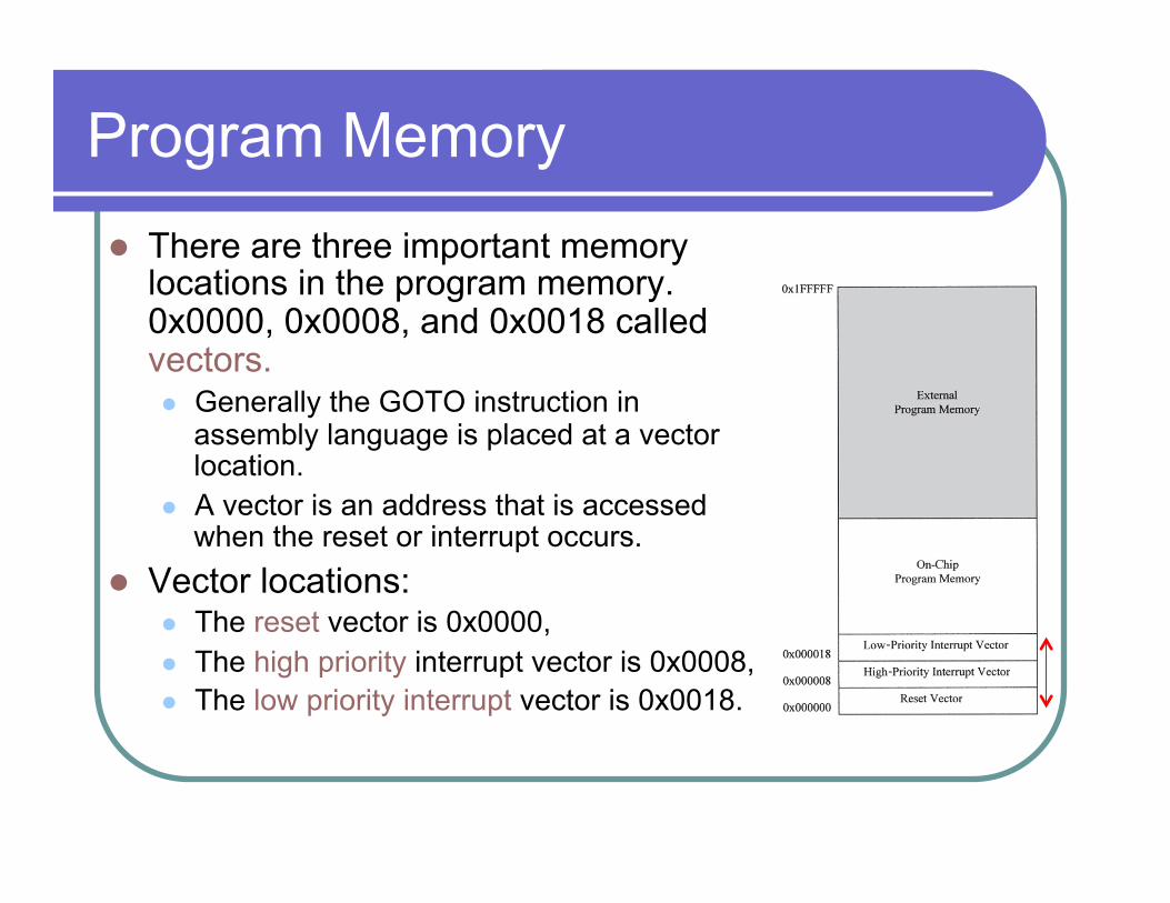
Program Memory l There are three important memory
locations in the program memory. 0x0000, 0x0008, and 0x0018 called vectors. l Generally the GOTO instruction in
assembly language is placed at a vector location.
l A vector is an address that is accessed when the reset or interrupt occurs.
l Vector locations: l The reset vector is 0x0000, l The high priority interrupt vector is 0x0008, l The low priority interrupt vector is 0x0018.
Accessing Program Memory
Let’s Review Directives First…
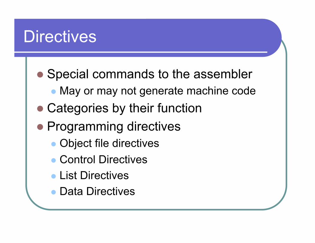
Directives
l Special commands to the assembler l May or may not generate machine code
l Categories by their function l Programming directives
l Object file directives l Control Directives l List Directives l Data Directives
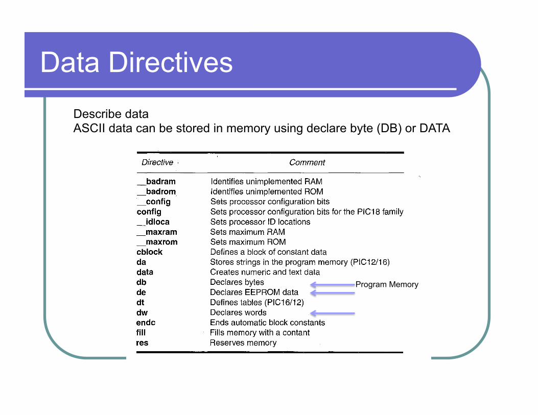
Data Directives Describe data ASCII data can be stored in memory using declare byte (DB) or DATA
Program Memory
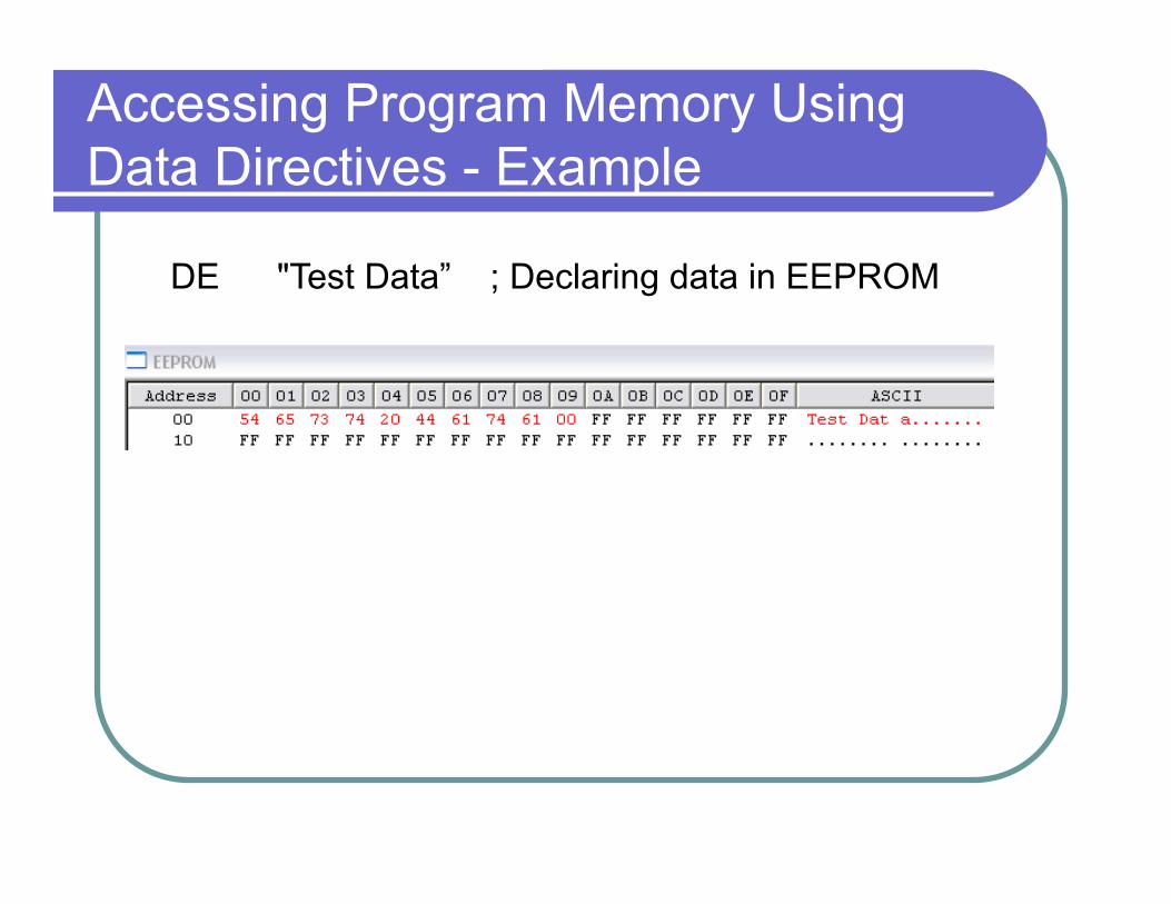
Accessing Program Memory Using Data Directives - Example
DE "Test Data” ; Declaring data in EEPROM
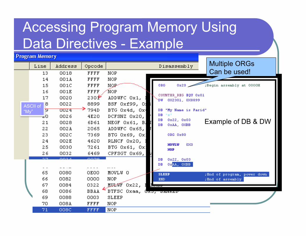
Accessing Program Memory Using Data Directives - Example
Example of DB & DW
Multiple ORGs Can be used!
ASCII of “My”
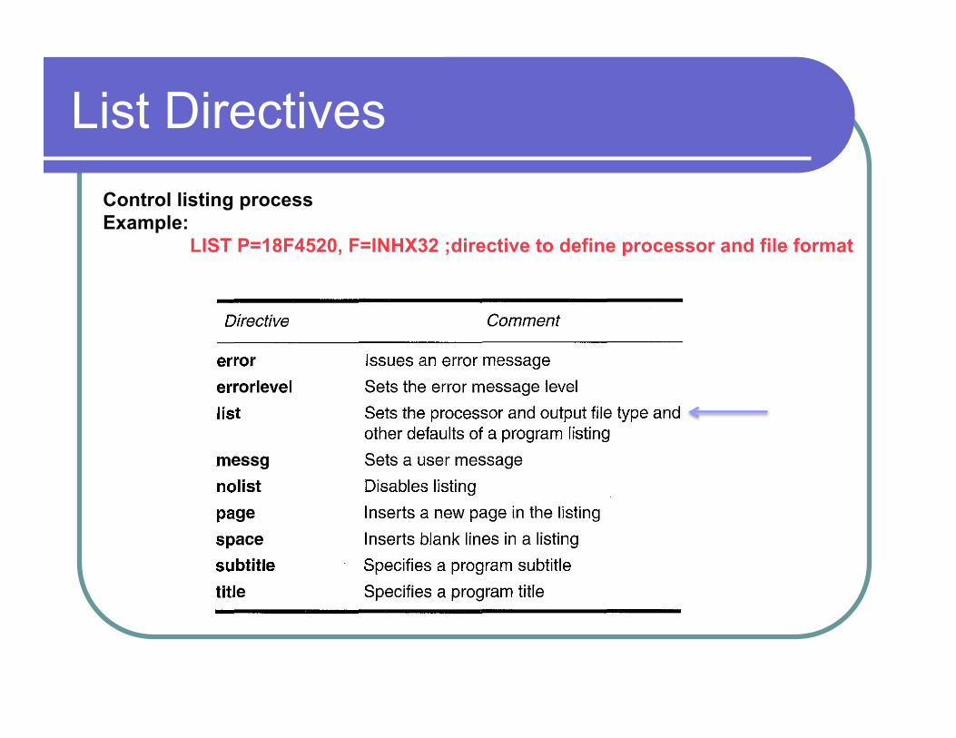
List Directives Control listing process Example:
LIST P=18F4520, F=INHX32 ;directive to define processor and file format
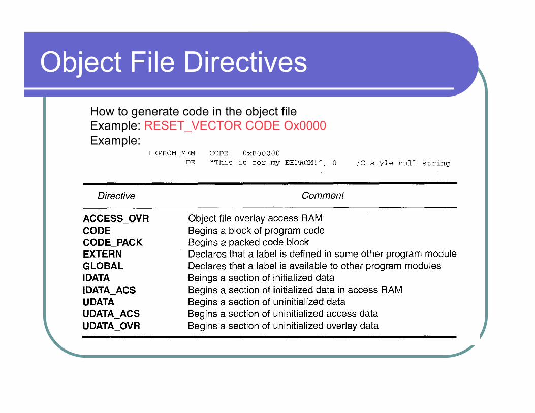
Object File Directives How to generate code in the object file Example: RESET_VECTOR CODE Ox0000 Example:
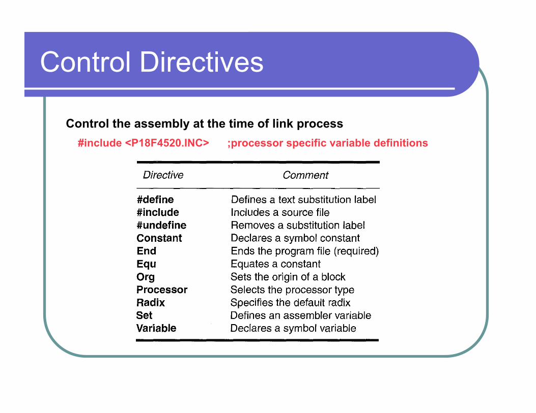
Control Directives
Control the assembly at the time of link process #include <P18F4520.INC> ;processor specific variable definitions
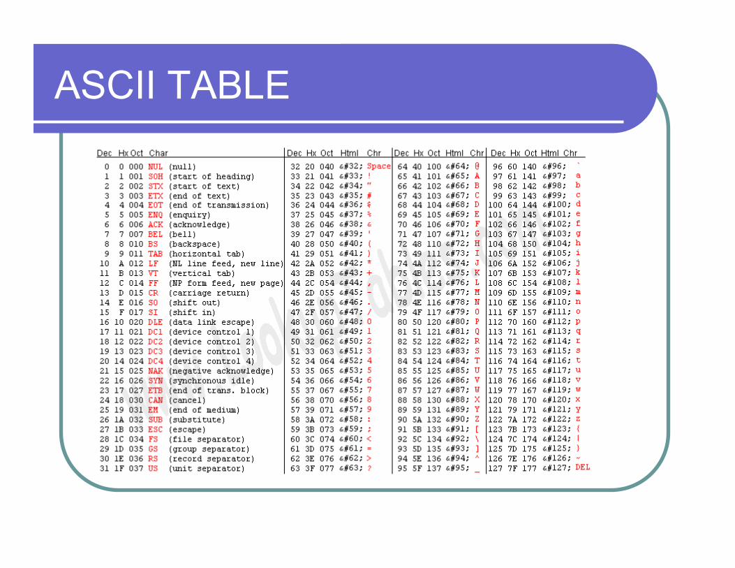
ASCII TABLE
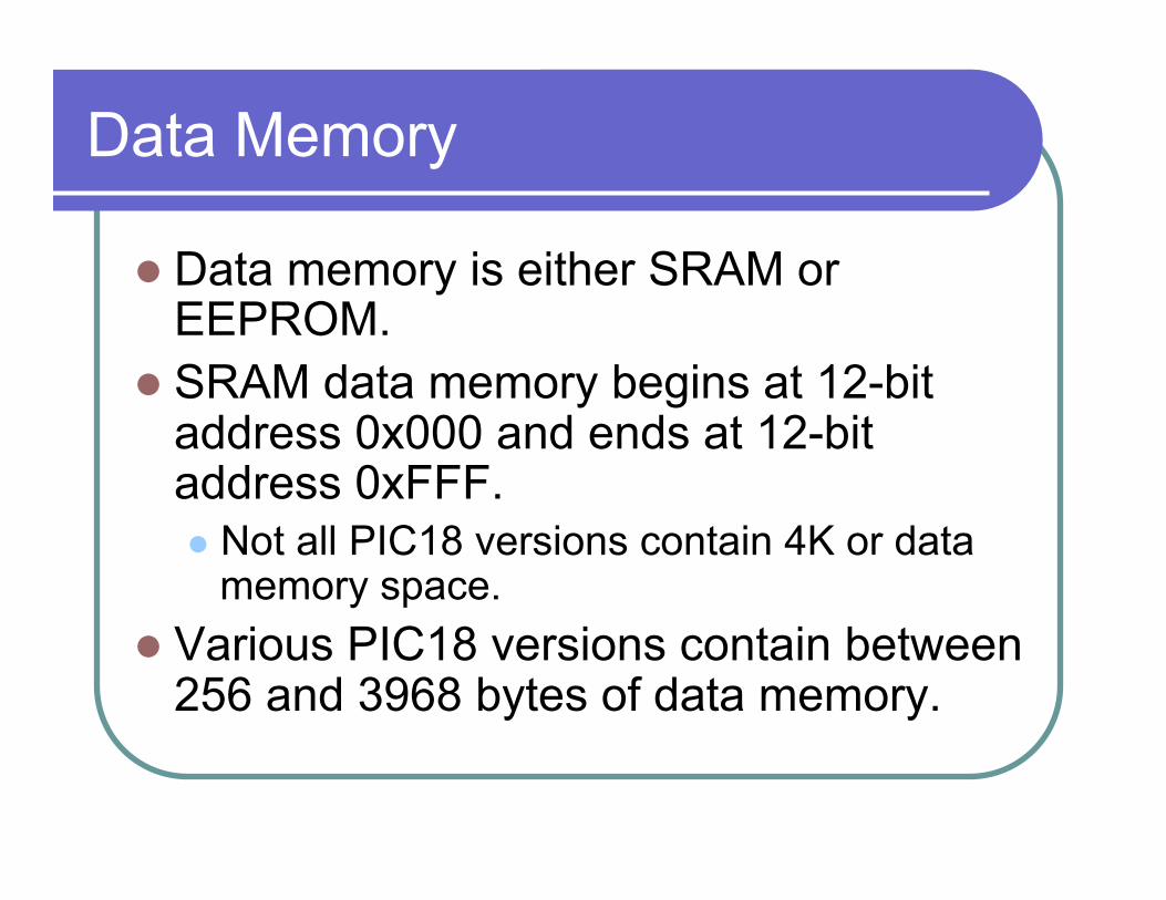
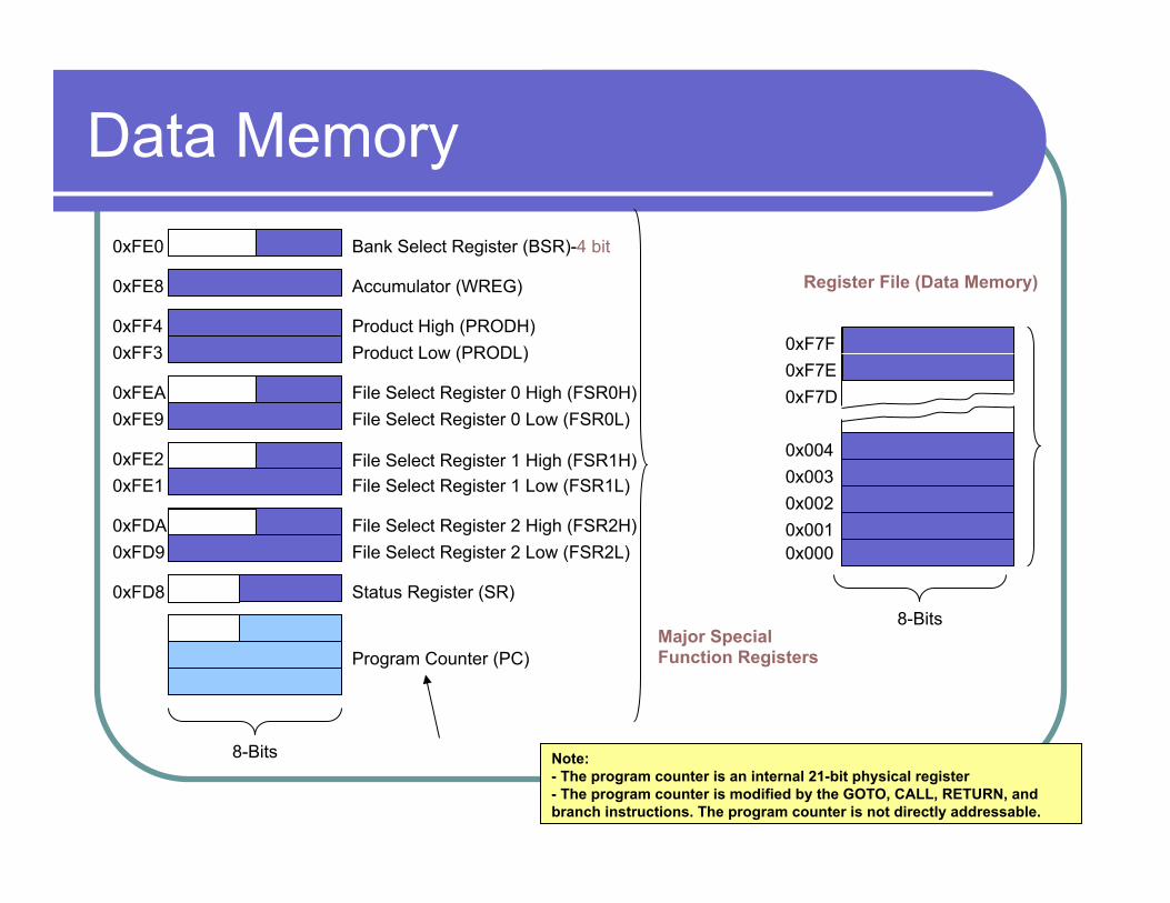
Data Memory
l Data memory is either SRAM or EEPROM.
l SRAM data memory begins at 12-bit address 0x000 and ends at 12-bit address 0xFFF. l Not all PIC18 versions contain 4K or data
memory space. l Various PIC18 versions contain between
256 and 3968 bytes of data memory.
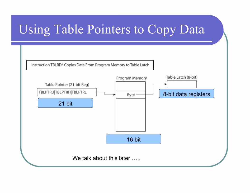
Using Table Pointers to Copy Data
21 bit
16 bit
8-bit data registers
We talk about this later …..

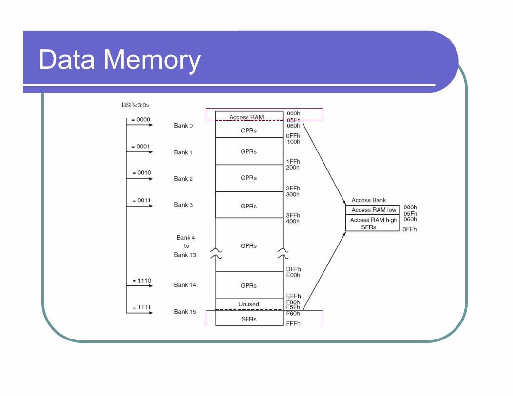
Data Memory
l There are two types of registers: l general-purpose registers (GPRs) l special-function registers (SFRs)
l GPRs are used to hold dynamic data when the PIC18 CPU is executing a program.
l SFRs are registers used by the CPU and peripheral modules for controlling the desired operation of the MCU.
l The upper 128 bytes of the data memory are used for special function registers (SFR) at addresses 0xF80 through 0xFFF. Some versions of the PIC18 have additional SFRs at locations below 0xF80.
Data Memory
Data Memory
0x000 0x001 0x002 0x003 0x004
Register File (Data Memory)
0xF7F 0xF7E 0xF7D
Bank Select Register (BSR)-4 bit Accumulator (WREG) Product High (PRODH) Product Low (PRODL)
0xFE8 0xFE0
Major Special Function Registers
0xFF3 0xFF4
File Select Register 0 High (FSR0H) File Select Register 0 Low (FSR0L)
File Select Register 1 High (FSR1H)
File Select Register 1 Low (FSR1L)
File Select Register 2 High (FSR2H)
File Select Register 2 Low (FSR2L)
0xFEA 0xFE9 0xFE2 0xFE1
0xFD9 0xFDA
Status Register (SR) 0xFD8
8-Bits
Program Counter (PC) 8-Bits
Note: - The program counter is an internal 21-bit physical register - The program counter is modified by the GOTO, CALL, RETURN, and branch instructions. The program counter is not directly addressable.
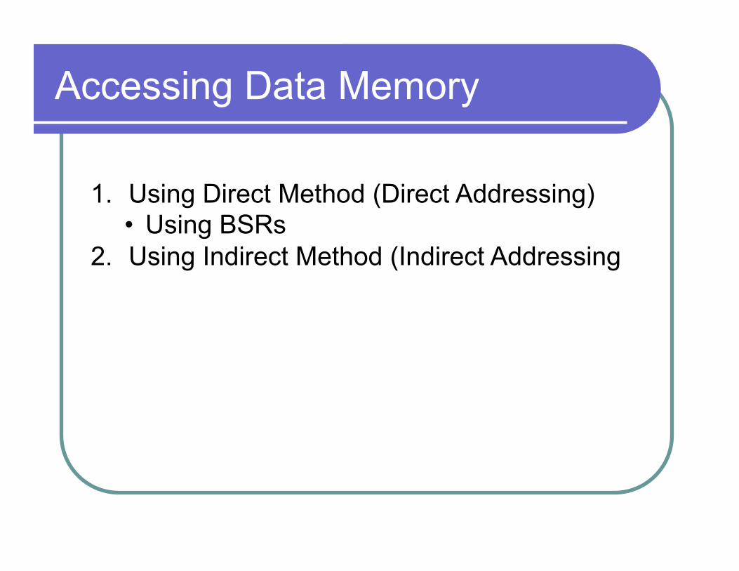
Accessing Data Memory
1. Using Direct Method (Direct Addressing) • Using BSRs
2. Using Indirect Method (Indirect Addressing
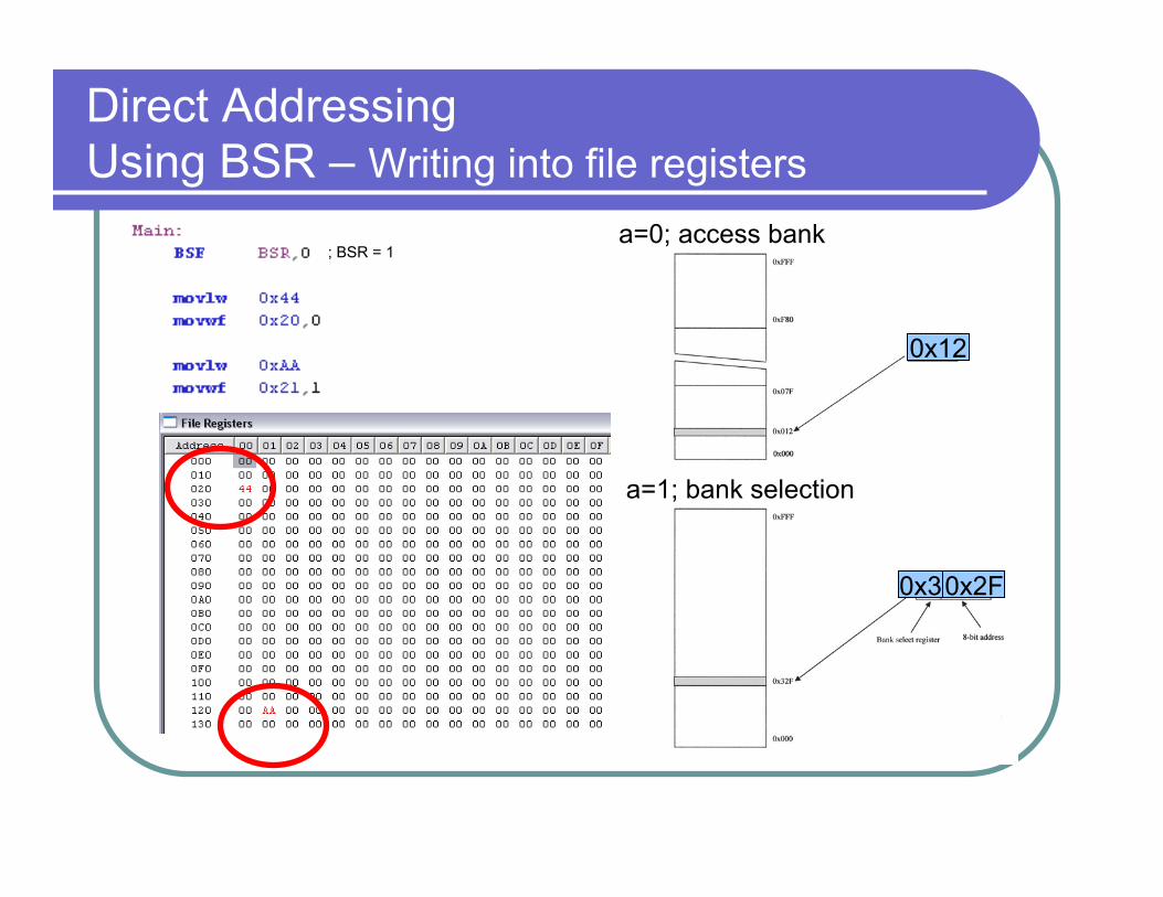
Direct Addressing Using BSR – Writing into file registers
0x12
0x2F 0x3
a=1; bank selection
a=0; access bank ; BSR = 1
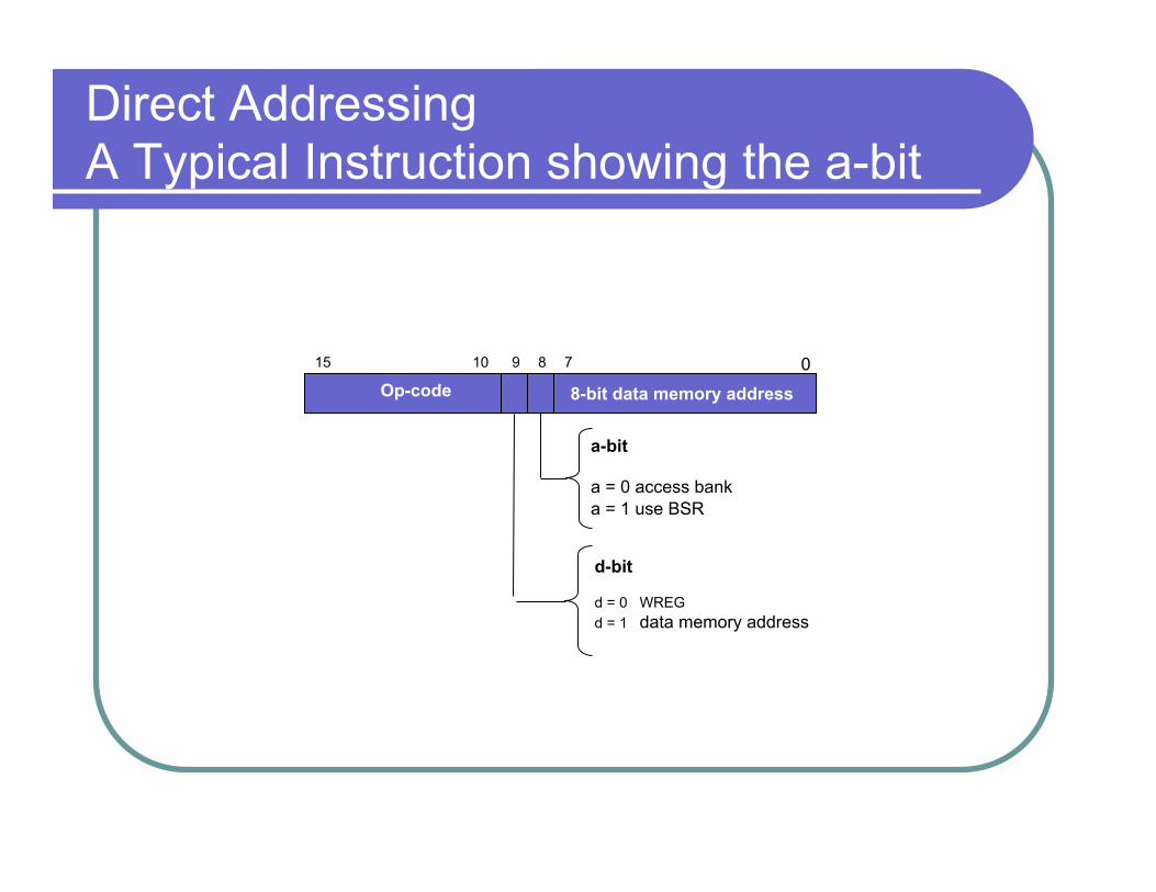
Direct Addressing A Typical Instruction showing the a-bit
15 10 9 8 7 0 Op-code 8-bit data memory address
a-bit a = 0 access bank a = 1 use BSR
d-bit d = 0 WREG d = 1 data memory address
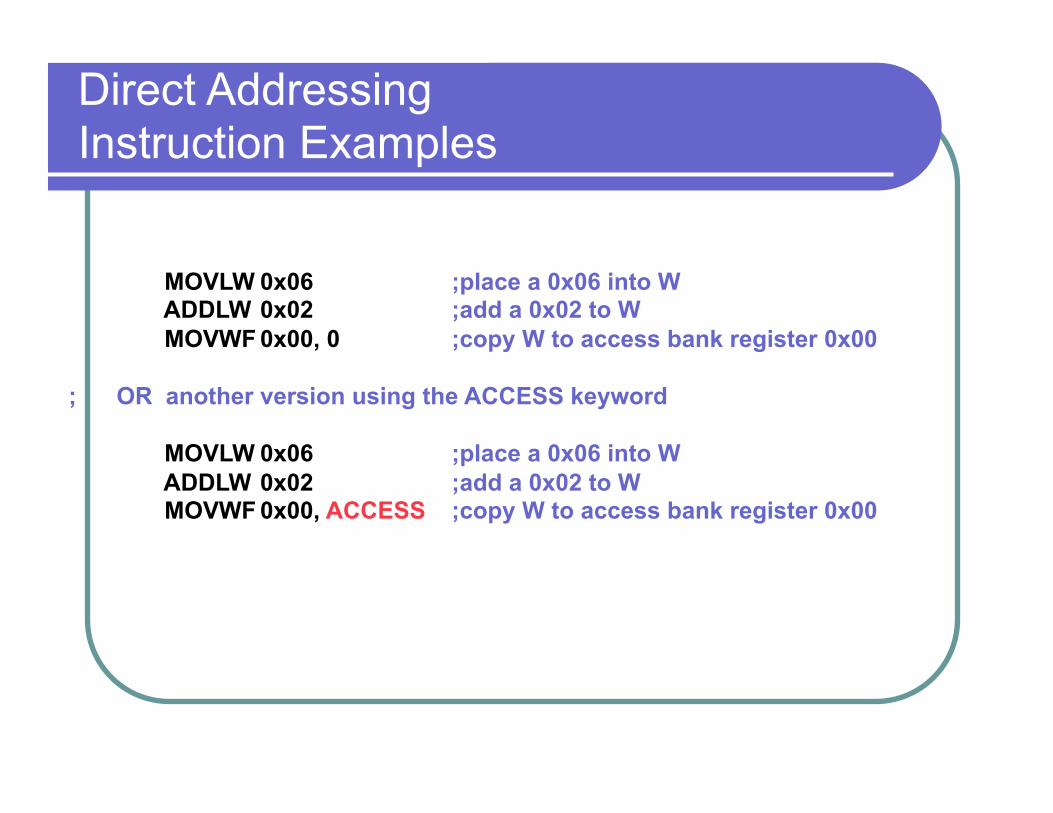
MOVLW 0x06 ;place a 0x06 into W ADDLW 0x02 ;add a 0x02 to W MOVWF 0x00, 0 ;copy W to access bank register 0x00
; OR another version using the ACCESS keyword MOVLW 0x06 ;place a 0x06 into W ADDLW 0x02 ;add a 0x02 to W MOVWF 0x00, ACCESS ;copy W to access bank register 0x00
Direct Addressing Instruction Examples
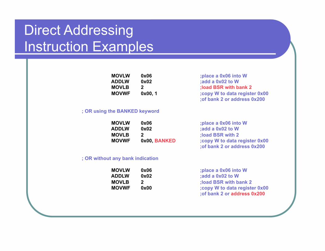
MOVLW 0x06 ;place a 0x06 into W ADDLW 0x02 ;add a 0x02 to W MOVLB 2 ;load BSR with bank 2 MOVWF 0x00, 1 ;copy W to data register 0x00 ;of bank 2 or address 0x200
; OR using the BANKED keyword
MOVLW 0x06 ;place a 0x06 into W ADDLW 0x02 ;add a 0x02 to W MOVLB 2 ;load BSR with 2 MOVWF 0x00, BANKED ;copy W to data register 0x00 ;of bank 2 or address 0x200
; OR without any bank indication MOVLW 0x06 ;place a 0x06 into W ADDLW 0x02 ;add a 0x02 to W MOVLB 2 ;load BSR with bank 2 MOVWF 0x00 ;copy W to data register 0x00 ;of bank 2 or address 0x200
Direct Addressing Instruction Examples

Indirect Addressing Using File Select Registers (FSRs) as Pointers
l Memory pointer is a register that holds the address of a data register l This is called indirect
addressing l Easy to move/copy an
entire block l Three pointer registers:
FSR0, FSR1, and FSR2
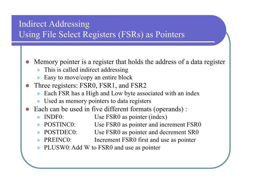
Indirect Addressing Using File Select Registers (FSRs) as Pointers
l Memory pointer is a register that holds the address of a data register l This is called indirect addressing l Easy to move/copy an entire block
l Three registers: FSR0, FSR1, and FSR2 l Each FSR has a High and Low byte associated with an index l Used as memory pointers to data registers
l Each can be used in five different formats (operands) : l INDF0: Use FSR0 as pointer (index) l POSTINC0: Use FSR0 as pointer and increment FSR0 l POSTDEC0: Use FSR0 as pointer and decrement SR0 l PREINC0: Increment FSR0 first and use as pointer l PLUSW0: Add W to FSR0 and use as pointer
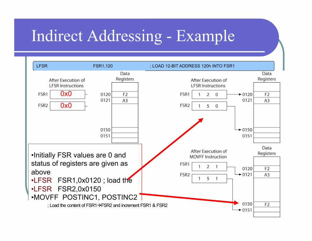
Indirect Addressing - Example LFSR FSR1,120 ; LOAD 12-BIT ADDRESS 120h INTO FSR1
• Initially FSR values are 0 and status of registers are given as above • LFSR FSR1,0x0120 ; load the • LFSR FSR2,0x0150 • MOVFF POSTINC1, POSTINC2
0x0
0x0
; Load the content of FSR1àFSR2 and increment FSR1 & FSR2
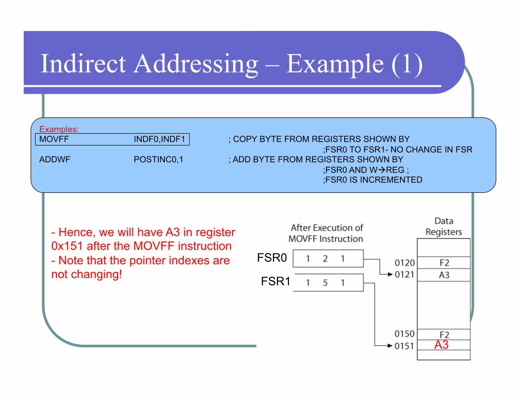
Indirect Addressing – Example (1)
Examples: MOVFF INDF0,INDF1 ; COPY BYTE FROM REGISTERS SHOWN BY
;FSR0 TO FSR1- NO CHANGE IN FSR ADDWF POSTINC0,1 ; ADD BYTE FROM REGISTERS SHOWN BY
;FSR0 AND WàREG ; ;FSR0 IS INCREMENTED
- Hence, we will have A3 in register 0x151 after the MOVFF instruction - Note that the pointer indexes are not changing!
A3
FSR0
FSR1
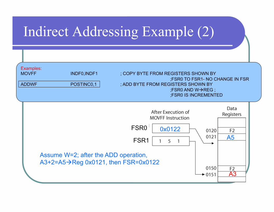
Indirect Addressing Example (2)
Assume W=2; after the ADD operation, A3+2=A5àReg 0x0121, then FSR=0x0122
A5 0x0122
Examples: MOVFF INDF0,INDF1 ; COPY BYTE FROM REGISTERS SHOWN BY
;FSR0 TO FSR1- NO CHANGE IN FSR ADDWF POSTINC0,1 ; ADD BYTE FROM REGISTERS SHOWN BY
;FSR0 AND WàREG ; ;FSR0 IS INCREMENTED
FSR0
FSR1
A3
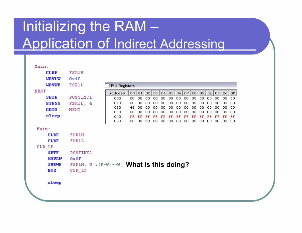
Initializing the RAM – Application of Indirect Addressing
What is this doing?
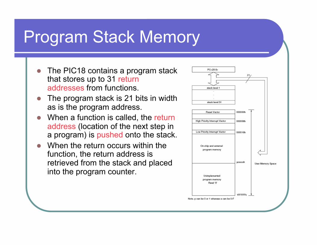
Program Stack Memory
l The PIC18 contains a program stack that stores up to 31 return addresses from functions.
l The program stack is 21 bits in width as is the program address.
l When a function is called, the return address (location of the next step in a program) is pushed onto the stack.
l When the return occurs within the function, the return address is retrieved from the stack and placed into the program counter.
Practice Program
l Save your first name into EEPROM starting Register 0x20 l Save your last name into EEPROM starting Register 0x80 l Save your first name into RAM starting Register 0x20 l Save your last name into RAM starting Register 0x80 l Write your last name in bank 2 starting with register 0x20 l Multiply 0x8 and 0x5 and leave the result in registers 0x50 of the
RAM in Bank 4 l What is the address of the PC SFR ? l Load FF into RAM registers 0x30-0x40. Use Indirect addressing
only!