Embed Size (px)
Citation preview
Fakultät Technik und Informatik
Department Informations- und
Elektrotechnik
Faculty of Engineering and Computer Science
Department of Information and
Electrical Engineering
Claus Alexander Höfs
Short Wave Receivers Comparison
implemented on DSP and FPGA
Diplomarbeit
Diplomarbeit eingereicht im Rahmen der Diplomprüfung im Studiengang Informations- und Elektrotechnik Studienrichtung Informationstechnik am Department Informations- und Elektrotechnik der Fakultät Technik und Informatik der Hochschule für Angewandte Wissenschaften Hamburg Betreuender Prüfer : Prof. Dr. Ulrich Sauvagerd Zweitgutachter : Prof. Dr.-Ing. Karl-Ragmar Riemschneider Abgegeben am 04. Juli 2007
Claus Alexander Höfs
Short Wave Receivers Comparison implemented on DSP
and FPGA
Claus Alexander Höfs Thema der Diplomarbeit Kurzwellenempfänger implementiert auf DSP und FPGA Stichworte Kurzwellenempfänger, DSP, FPGA, MicroBlaze, Signalunterabtastung Kurzzusammenfassung In dieser Arbeit wurde ein Kurzwellenempfänger mit Hilfe eines Produktdemodulators zuerst auf einem DSP und anschließend auf einem FPGA implementiert. Dazu wurde ein A/D-D/A-Umsetzer der Firma DSignT über eine Adapterkarte an den DSP C6713 angeschlossen und ein C-Programm entworfen, welches den Umsetzer anspricht, ihn initialisiert und in einer Interrupt-Service-Routine mit ihm kommuniziert. In der Interrupt-Service-Routine findet auch die Demodulation des empfangenen Signals statt. Anschließend wurden mit Hilfe eines Logik-Analysators alle Signale analysiert, die zu dem Umsetzer gehen. Daraufhin wurde anhand der Ergebnisse, der Analyse des Logik- Analysators, ein VHDL Programm erstellt, welches es ermöglicht auf einem FPGA das Ergebnis des Logik-Analysators wiederzugeben. Anschließend wurde das gleiche C-Programm wie auf dem DSP auf einem MicroBlaze implementiert, dieser ist ein Softprozessorkern welcher im FPGA relativ leicht einzufügen ist. Es dient somit das gleiche C-Programm auf beiden Systemen und es konnte dadurch ein guter Vergleich beider Systeme erstellt werden. Claus Alexander Höfs Title of the paper Short Wave Receivers Comparison implemented on DSP and FPGA Keywords short wave receiver, DSP, FPGA, MicroBlaze, signal down sampling Abstract In this work a shortwave receiver was implemented with the help of a product demodulators first on a DSP, and afterwards on a FPGA. In addition an adaptor to the DSP C6713 is connected to an A/D D/A converter of the company DsignT. A c- program was written which interacts with the converter, initializes it and communicates with the interrupt service routine. The demodulation of the received signal also takes place in the interrupt service routine. Afterwards all signals were analyzed with the help of a logic analyzer. As a result of the logic analyzer a program in VHDL was developed. It enables the programm to reproduce the result of the logic analyzer on a FPGA. Afterwards the same C program was implemented on a MicroBlaze as well as on DSP. This is a soft processor core that should be easily implemented on the FPGA. So the same c- program runs on both systems and a good comparison should be done.
i
Contents
List of Figures iii
List of Tables v
Acknowledgement vi
1 Introduction 1
1.1 Motivation..................................................................................................... 1
1.2 Specifications ............................................................................................... 1
1.2.1 AM Receiver Architecture ..................................................................... 1
1.2.2 The Signals ........................................................................................... 2
2 Theory 3
2.1 Amplitude Modulation................................................................................... 3
2.2 Algorithms for Signal Pretreatment............................................................... 3
2.2.1 Sub Sampling........................................................................................ 4
2.2.2 Quadrature Sampling ............................................................................ 7
2.3 Algorithm for Digital AM Demodulation....................................................... 10
3 Implementation 12
3.1 Preliminary work......................................................................................... 12
3.1.1 Main Program...................................................................................... 12
3.1.2 Interrupt Service Routine (ISR) ........................................................... 12
3.2 ADDA16 ..................................................................................................... 14
3.2.1 Description .......................................................................................... 14
3.2.2 Address Decoding............................................................................... 14
3.2.3 Configuration Register (CFG).............................................................. 16
3.2.4 Sampling Frequency Register (FS) ..................................................... 16
3.2.5 Bus Interface....................................................................................... 17
3.3 DSP............................................................................................................ 17
3.3.1 Description .......................................................................................... 17
3.3.2 Software.............................................................................................. 18
3.3.3 External Memory Interface (EMIF) on C6713...................................... 18
3.3.4 Address Decoding............................................................................... 19
3.4 Signal Analyze with Logic Analyzer............................................................ 20
3.4.1 Generics to the Analyzer Pictures ....................................................... 20
ii
3.4.2 Reset Cycle......................................................................................... 21
3.4.3 Initial Procedure .................................................................................. 21
3.4.4 Release of the Interrupt Request Signal nINT0................................... 22
3.4.5 Complete Interrupt Function................................................................ 22
3.4.6 First Part of Interrupt Function............................................................. 23
3.4.7 Middle Part of Interrupt Function ......................................................... 23
3.4.8 Last Part of Interrupt Function............................................................. 23
3.4.9 A Typical Read Procedure .................................................................. 25
3.4.10 A Typical Write Procedure .................................................................. 26
3.5 FPGA with Xilinx MicroBlaze...................................................................... 27
3.5.1 Description .......................................................................................... 28
3.5.2 Introduction ......................................................................................... 28
3.5.3 Instantiable Cores ............................................................................... 29
3.5.4 Interrupt Controller .............................................................................. 30
3.5.5 Block RAM .......................................................................................... 30
3.5.6 Own Core............................................................................................ 31
3.5.7 Create or Import Peripheral Wizard..................................................... 31
3.5.8 Microprocessor Peripheral Definition (MPD) ....................................... 36
3.5.9 Microprocessor Hardware Specification (MHS)................................... 37
3.5.10 User Constraint File (UCF).................................................................. 40
3.5.11 Access to Own Core ........................................................................... 40
3.5.12 User Logic from Own Core.................................................................. 41
3.5.13 Interface from Own Core..................................................................... 42
3.5.14 Address Decoding............................................................................... 44
3.6 Complex Programmable Logic Device (CPLD) .......................................... 44
3.6.1 Bus Driver with CPLD ......................................................................... 44
3.6.2 Stand Alone CPLD .............................................................................. 45
3.6.3 The Answer to This Problem............................................................... 46
4 Comparison of Both Implementations 47
5 Conclusions and Recommendations 48
A. Abbreviations 49
B. Bibliography 51
iii
List of Figures
Figure 1.1: Block Diagram AM Receiver Architecture ............................................. 1
Figure 1.2: Spectrum of the Message Signal .......................................................... 2
Figure 1.3: Spectrum of the AM Signal ................................................................... 2
Figure 2.1: Subdivisions of AM Demodulation Block............................................... 3
Figure 2.2: Subdivisions of AM Demodulation Block, now Sub Sampling ............... 4
Figure 2.3: Spectrum of Sub Sampling with Even λ ................................................ 5
Figure 2.4: Spectrum of Sub Sampling with Odd λ ................................................. 6
Figure 2.5: Subdivisions of AM Demodulation Block, now Quadrature Mixing ........ 7
Figure 2.6: Realising the Mixer with a Real Signal .................................................. 7
Figure 2.7: Down Quadrature Mixer without Hilbert Transformation ....................... 8
Figure 2.8: Delayed Sampling ................................................................................. 8
Figure 2.9: Realization of the Delayed Sampling .................................................... 9
Figure 2.10 Subdivisions of AM Demodulation Block, now Demodulation.......... 10
Figure 2.11: Product Demodulator....................................................................... 11
Figure 2.12: Absolute Value Calculation.............................................................. 11
Figure 3.1: General Program Flow ........................................................................ 12
Figure 3.2: Program Flow of ISR........................................................................... 13
Figure 3.3: ADDA16 Overview .............................................................................. 14
Figure 3.4: Block Diagram AM Receiver Architecture with DSP............................ 17
Figure 3.5: Complete Reset Cycle ........................................................................ 21
Figure 3.6: Initial Procedure .................................................................................. 21
Figure 3.7: Release of Interrupt............................................................................. 22
Figure 3.8: Complete Interrupt Function................................................................ 22
Figure 3.9: First Part of Interrupt Function............................................................. 23
Figure 3.10: Middle Part of Interrupt Function ..................................................... 23
Figure 3.11: Last Part of Interrupt Function ......................................................... 24
Figure 3.12: A Typical Read Procedure............................................................... 25
Figure 3.13: A Typical Write Procedure ............................................................... 26
Figure 3.14: XUP Virtex-II Pro Development System .......................................... 27
Figure 3.15: Block Diagram AM Receiver Architecture with FPGA...................... 28
Figure 3.16: MicroBlaze Core Block Diagram...................................................... 29
Figure 3.17: Interrupt Controller Block Diagram .................................................. 30
iv
Figure 3.18: IPIF Interconnection Between OPB and Own Core [X3].................. 31
Figure 3.19: Create Peripheral - Name and Version............................................ 32
Figure 3.20: Create Peripheral - IPIF Services .................................................... 33
Figure 3.21: Create Peripheral – Interrupt Service .............................................. 34
Figure 3.22: Create Peripheral – User S/W Register ........................................... 35
Figure 3.23: IOBUF Implementation .................................................................... 37
Figure 3.24: System Assembly View ................................................................... 37
Figure 3.25: Modyfing Bus Connections .............................................................. 38
Figure 3.26: Changing Port Connections............................................................. 39
Figure 3.27: Generate Addresse ......................................................................... 39
Figure 3.28: Block Diagram AM Receiver Architecture with FPGA and CPLD .... 45
Figure 3.29: System Block Diagram with Stand Alone CPLD.............................. 45
v
List of Tables
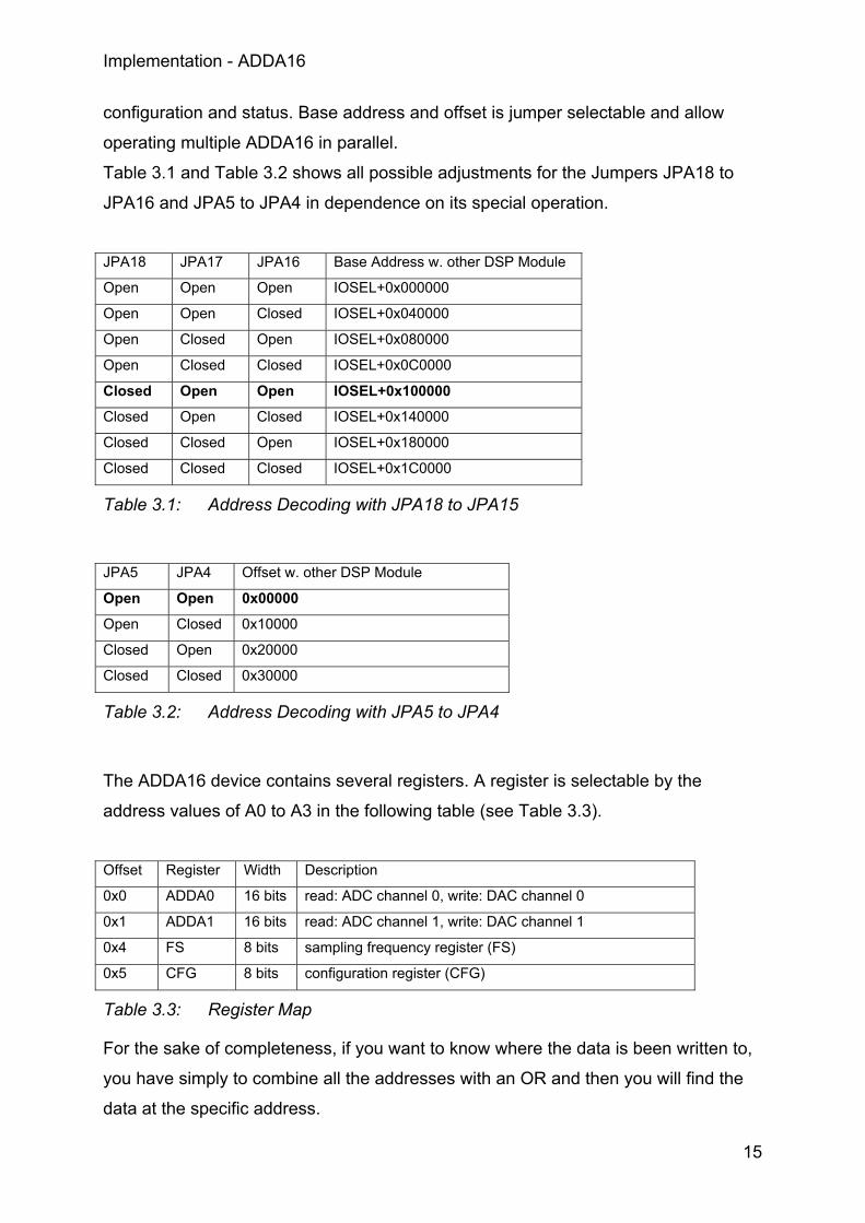
Table 3.1: Address Decoding with JPA18 to JPA15 ............................................ 15
Table 3.2: Address Decoding with JPA5 to JPA4 ................................................ 15
Table 3.3: Register Map....................................................................................... 15
Table 3.4: Potential Settings in the Configuration Register .................................. 16
Table 3.5: Pin Connection.................................................................................... 17
Table 3.6: EMIF Timing on C6713 ....................................................................... 18
Table 3.7: TMS320C621x/C671x Addressable Memory Ranges......................... 19
Table 3.8: Address Space of CE3........................................................................ 19
Table 3.9: Address Mapping with the JPA’s......................................................... 19
Table 4.1: Comparison of optimization levels....................................................... 47

vi
Acknowledgement Without the support of many people, this diploma thesis would not have been
possible. At this point I would like to express our appreciation to all persons who
were involved.
Thanks to Prof. Dr. Ulrich Sauvagerd, University of Applied Sciences (HAW)
Hamburg, for his encouraging support during the whole time of this work. Prof. Dr.-
Ing. Karl-Ragmar Riemschneider, HAW Hamburg, for his help on reviewing the
report. Mr Klemenz, developer of company DSignT, for his friendly assistance during
several calls. Mr Pflüger and Mr Wolf, the assistants of the laboratory for digital
techniques, University of Applied Sciences (HAW) Hamburg, for their friendly
support. Mrs. Pflänzel and Mr. Fellbrich, also for reviewing of the report. I would like
to thank the students in the laboratory who supported me in any form.
Introduction - Motivation
1
1 Introduction
1.1 Motivation
Amplitude modulation (AM) is an analog modulation, which is for example used in
radio frequency (RF) broadcasting.
Another field of application for AM are weather news services, which were digital
encoded or amateur radio users.
A digital counterpart will gradually replace those analog systems in the new
generation. For a smooth transition of the two systems, it is essential for the new
generation system to be able to communicate with the radio equipment of the old
generation. Because all the new radio equipment are based on Digital Signal
Processor (DSP) -Technology, it is obvious and of commercial interest to perform the
demodulation with the signal processor instead of adding additional analog hardware.
1.2 Specifications
1.2.1 AM Receiver Architecture
The amplitude-modulated signal (sAM) is frequency limited at an intermediate
frequency (IF) of 455 kHz. The antenna and tuner are given and do not fall in the
scope of this work. (see Figure 1.1).
Tuner SystemSAM Sout
LS
Figure 1.1: Block Diagram AM Receiver Architecture
Legend for Figure 1.1:
sout out signal to Speaker
LS Loud Speaker
Introduction - Specifications
2
1.2.2 The Signals
The message signal sAM is a speech and music signal from 0 Hz to 4000 Hz. [SIG1]
(see Figure 1.2)
Figure 1.2: Spectrum of the Message Signal
The message signal sAM has a bandwidth (b) of 8 kHz and a carrier frequency (fT) of
455 kHz. (see Figure 1.3)
Figure 1.3: Spectrum of the AM Signal
1k 2k 3k 4k f(Hz)
A
message signal
b = 4000Hz
455k f(Hz)
A
AM signal
b = 8000Hz
Theory - Amplitude Modulation
3
2 Theory
2.1 Amplitude Modulation
AM is also called a linear modulation, so it is simply the use of the frequency-shifting
theorem. A conventional amplitude modulated signal is defined by the following
equation, which is described in [HL04]
( ) ( ) ( )( ) ( )( )
−+++= tmtmtsts MTMTTTAM ωωωωω cos
2cos
2cosˆ ( 2.1)
It’s the result of a multiplication of two signals: a carrier-frequency sT(t) and a
modulated signal sM(t).
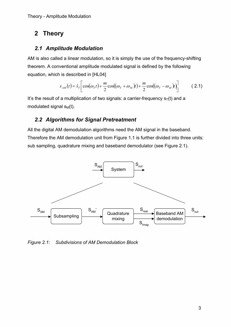
2.2 Algorithms for Signal Pretreatment
All the digital AM demodulation algorithms need the AM signal in the baseband.
Therefore the AM demodulation unit from Figure 1.1 is further divided into three units:
sub sampling, quadrature mixing and baseband demodulator (see Figure 2.1).
SystemSAM
Sout
SubsamplingSAM SAM’
Quadraturemixing
Simag
Baseband AMdemodulation
Sreal Sout
Figure 2.1: Subdivisions of AM Demodulation Block
Theory - Algorithms for Signal Pretreatment
4
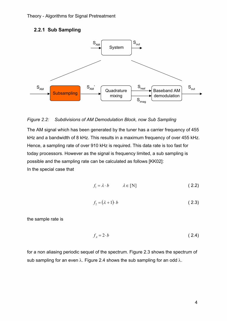
2.2.1 Sub Sampling
SystemSAM
Sout
SubsamplingSAM SAM’
Quadraturemixing
Simag
Baseband AMdemodulation
Sreal Sout
Figure 2.2: Subdivisions of AM Demodulation Block, now Sub Sampling
The AM signal which has been generated by the tuner has a carrier frequency of 455
kHz and a bandwidth of 8 kHz. This results in a maximum frequency of over 455 kHz.
Hence, a sampling rate of over 910 kHz is required. This data rate is too fast for
today processors. However as the signal is frequency limited, a sub sampling is
possible and the sampling rate can be calculated as follows [KK02]:
In the special case that
bf ⋅= λ1 ][Ν∈λ ( 2.2)
( ) bf ⋅+= 12 λ ( 2.3)
the sample rate is
bfA ⋅= 2 ( 2.4)
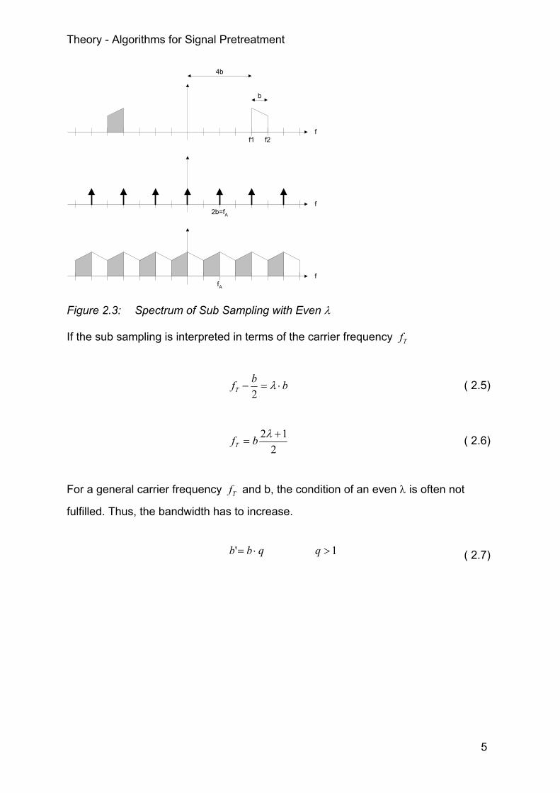
for a non aliasing periodic sequel of the spectrum. Figure 2.3 shows the spectrum of
sub sampling for an even λ. Figure 2.4 shows the sub sampling for an odd λ.
Theory - Algorithms for Signal Pretreatment
5
f1 f2
b
4b
f
2b=fAf
ffA
Figure 2.3: Spectrum of Sub Sampling with Even λ
If the sub sampling is interpreted in terms of the carrier frequency Tf
bbfT ⋅=− λ2
( 2.5)
212 +
=λbfT ( 2.6)
For a general carrier frequency Tf and b, the condition of an even λ is often not
fulfilled. Thus, the bandwidth has to increase.
qbb ⋅=' 1>q ( 2.7)
Theory - Algorithms for Signal Pretreatment
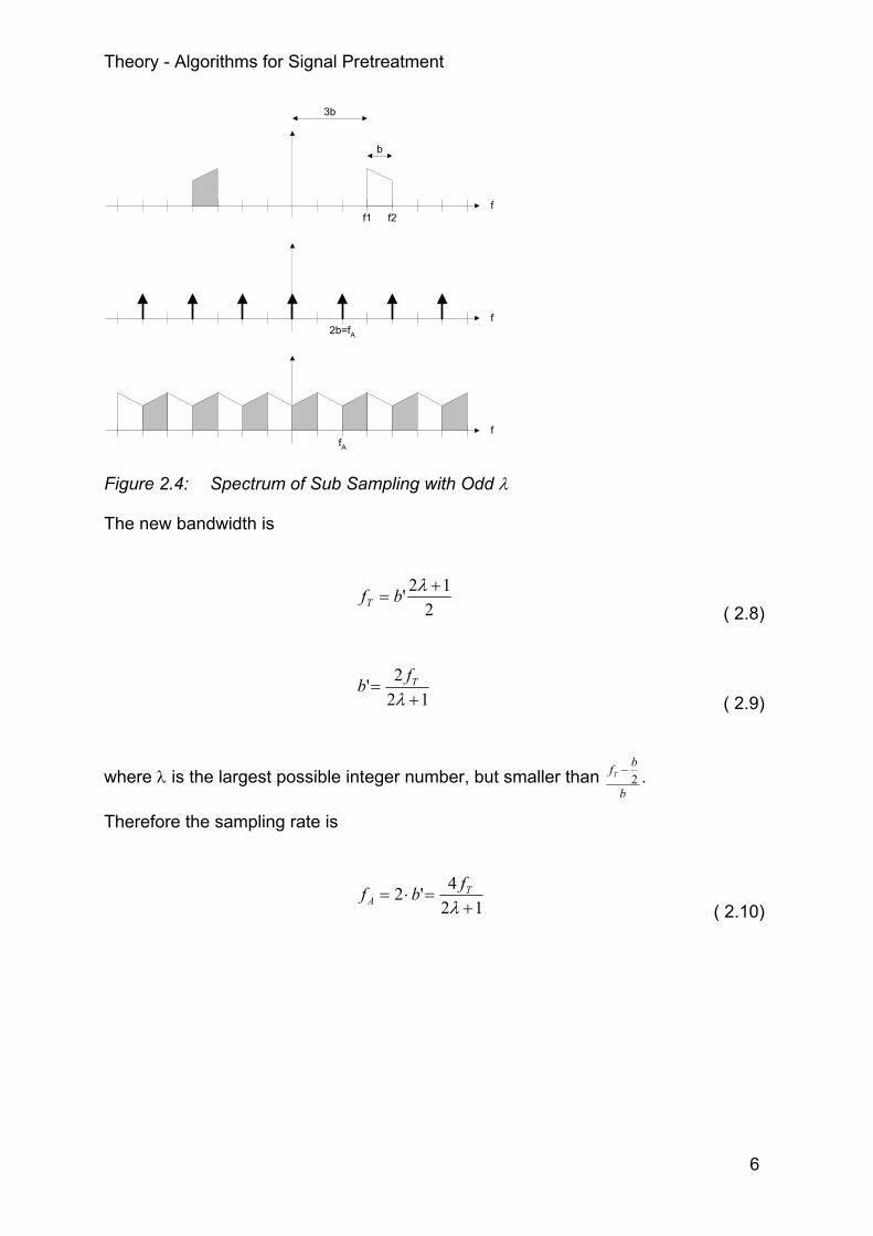
6
f1 f2
b
3b
f
2b=fAf
ffA
Figure 2.4: Spectrum of Sub Sampling with Odd λ
The new bandwidth is
212' +
=λbfT
( 2.8)
122'
+=
λTfb
( 2.9)
where λ is the largest possible integer number, but smaller than b
bfT 2− .
Therefore the sampling rate is
124'2
+=⋅=
λT
Afbf
( 2.10)
Theory - Algorithms for Signal Pretreatment
7
2.2.2 Quadrature Sampling
SystemSAM
Sout
SubsamplingSAM SAM’
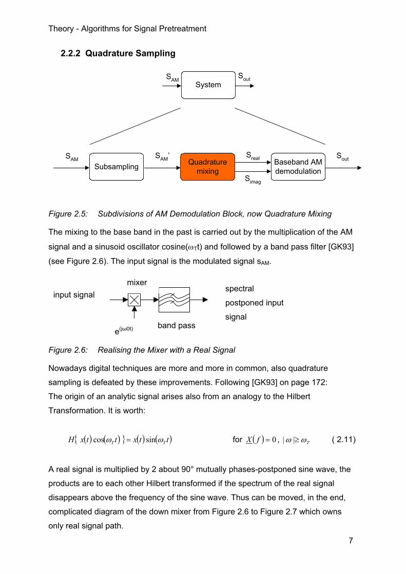
Quadraturemixing
Simag
Baseband AMdemodulation
Sreal Sout
Figure 2.5: Subdivisions of AM Demodulation Block, now Quadrature Mixing
The mixing to the base band in the past is carried out by the multiplication of the AM
signal and a sinusoid oscillator cosine(ωTt) and followed by a band pass filter [GK93]
(see Figure 2.6). The input signal is the modulated signal sAM.
Figure 2.6: Realising the Mixer with a Real Signal
Nowadays digital techniques are more and more in common, also quadrature
sampling is defeated by these improvements. Following [GK93] on page 172:
The origin of an analytic signal arises also from an analogy to the Hilbert
Transformation. It is worth:
( ) ( ){ } ( ) ( )ttxttxH TT ωω sincos = for ( ) 0=fX , Tωω ≥|| ( 2.11)
A real signal is multiplied by 2 about 90° mutually phases-postponed sine wave, the
products are to each other Hilbert transformed if the spectrum of the real signal
disappears above the frequency of the sine wave. Thus can be moved, in the end,
complicated diagram of the down mixer from Figure 2.6 to Figure 2.7 which owns
only real signal path.
input signal mixer
e(jω0t) band pass
spectral
postponed input
signal
Theory - Algorithms for Signal Pretreatment
8
Figure 2.7: Down Quadrature Mixer without Hilbert Transformation
Further on [GK93] page 181:
The system diagram after Figure 2.7 contains multipliers for the down sampling in the
zero position and in the model representation of the sampler, hence it should be
possible to reach the down sampling in zero position by the sampler himself, and
90°- shifting of the both sine waves, how in Figure 2.8 shown, is taken into
consideration by a time offset within the scanning.
Figure 2.8: Delayed Sampling
After the various reshaping which follows [GK93] on page 181 and the following and
which were not a subject of this diploma thesis, the following is important:
( ) ( ) ( )∑∑∞
=
∞
−∞=
+=−=1
2cos21k
an
AAper tkfnTtTt πδδ ( 2.12)
It ends with: At the exit of the low pass filter forming the signals of the cosine channel
( ) ( ) ( )ffUffUfU NFNF ∆++∆−=21
21
cos ( 2.13)
sin(ω0t)
cos(ω0t)
sAM(t)
( )∑∞
−∞=
−−=n
AAvper TntTt τδδ )(
uBP(t) ( )∑∞
−∞=
−=n
AAper TntTt δδ )(
uBPcosa(t)
uBPsina(t)
Theory - Algorithms for Signal Pretreatment
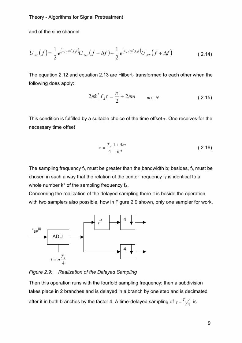
9
and of the sine channel
( ) ( ) ( ) ( ) ( )ffUeffUefU NFfkj
NFfkj AA ∆++∆−= +− τπτπ ** 22
sin 21
21
( 2.14)
The equation 2.12 and equation 2.13 are Hilbert- transformed to each other when the
following does apply:
mfk A ππτπ 22
2 * += Nm∈ ( 2.15)
This condition is fulfilled by a suitable choice of the time offset τ. One receives for the
necessary time offset
*41
4 kmTA +
=τ ( 2.16)
The sampling frequency fA must be greater than the bandwidth b; besides, fA must be
chosen in such a way that the relation of the center frequency fT is identical to a
whole number k* of the sampling frequency fA.
Concerning the realization of the delayed sampling there it is beside the operation
with two samplers also possible, how in Figure 2.9 shown, only one sampler for work.
Figure 2.9: Realization of the Delayed Sampling
Then this operation runs with the fourfold sampling frequency; then a subdivision
takes place in 2 branches and is delayed in a branch by one step and is decimated
after it in both branches by the factor 4. A time-delayed sampling of 4AT=τ is
uBP
(t)
ADU
z-1 4
4
4ATnt =
Theory - Algorithm for Digital AM Demodulation
10
thereby realized. In this case the sampling frequency must be chosen in such a way
that
*41 km =+ ( 2.17)
is true.
2.3 Algorithm for Digital AM Demodulation
Because of understandable reasons, like time and amount of work in this diploma
thesis, I describe only one easy way for demodulation and not the lot of types for
demodulation.
SystemSAM
Sout
SubsamplingSAM SAM’
Quadraturemixing
Simag
Baseband AMdemodulation
Sreal Sout
Figure 2.10 Subdivisions of AM Demodulation Block, now Demodulation
The product demodulator is the simplest demodulator in the digitalized world. The
product demodulator needs the AM signal in the baseband. Figure 2.11 shows the
block diagram of the complex product demodulator. The input signal is the RF AM
signal UHF(n), says [GK93] on page 200.
Theory - Algorithm for Digital AM Demodulation
11
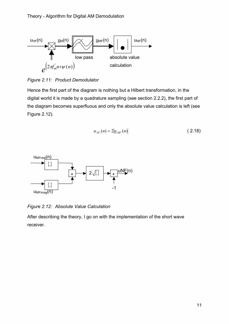
Figure 2.11: Product Demodulator
Hence the first part of the diagram is nothing but a Hilbert transformation, in the
digital world it is made by a quadrature sampling (see section 2.2.2), the first part of
the diagram becomes superfluous and only the absolute value calculation is left (see
Figure 2.12).
)(2)( nunu MFNF = ( 2.18)
Figure 2.12: Absolute Value Calculation
After describing the theory, I go on with the implementation of the short wave
receiver.
uM(n)
absolute value
calculation
uMF(n) uNF(n)
low pass
uHF(n)
( ))(2 ' nnfme ψπ +
uNF(n)
{}.
{}.
+ 2 {}. +
-1
uMFreal(n)
uMFimag(n)
Implementation - Preliminary work
12
3 Implementation
3.1 Preliminary work
I decided to use only one program for both implementations. The advantage is an
easier use and a better understanding. The disadvantage is that the FPGA is
programmed in a way to understand a C- program. The C- program could be split
into two huge sections, the main program flow and the interrupt routine.
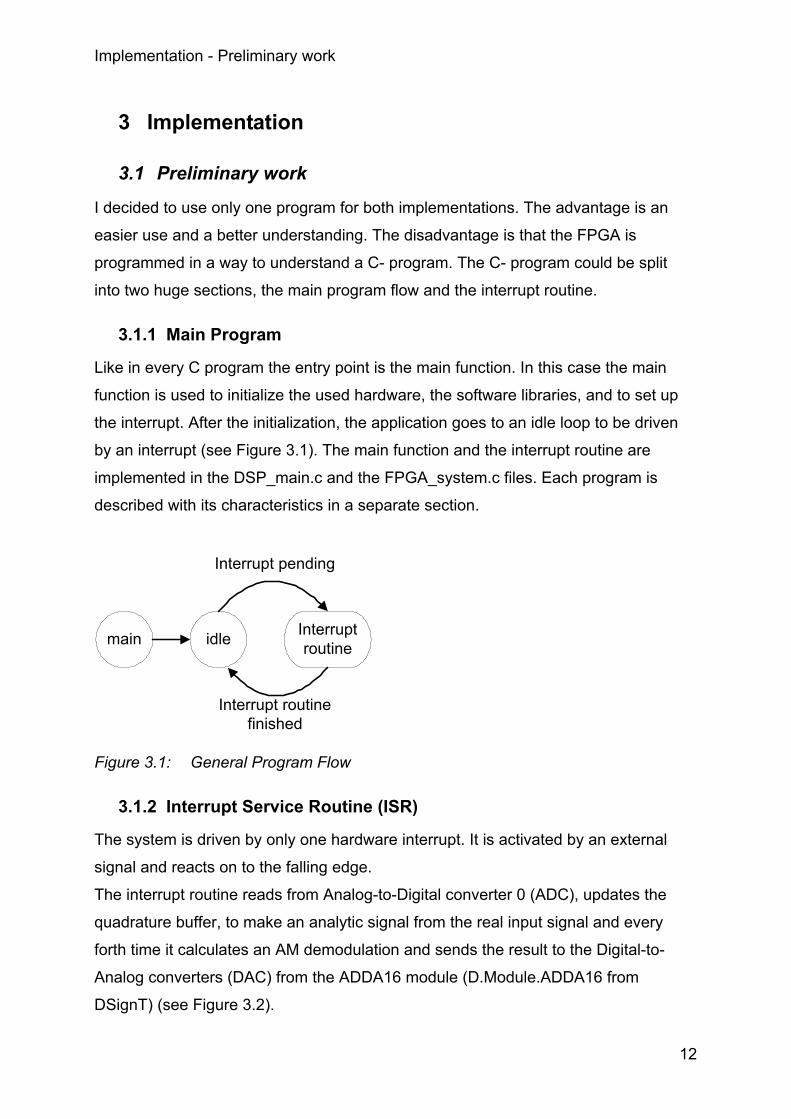
3.1.1 Main Program
Like in every C program the entry point is the main function. In this case the main
function is used to initialize the used hardware, the software libraries, and to set up
the interrupt. After the initialization, the application goes to an idle loop to be driven
by an interrupt (see Figure 3.1). The main function and the interrupt routine are
implemented in the DSP_main.c and the FPGA_system.c files. Each program is
described with its characteristics in a separate section.
main idle Interruptroutine
Interrupt pending
Interrupt routinefinished
Figure 3.1: General Program Flow
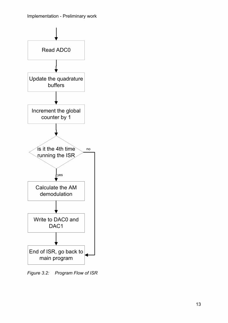
3.1.2 Interrupt Service Routine (ISR)
The system is driven by only one hardware interrupt. It is activated by an external
signal and reacts on to the falling edge.
The interrupt routine reads from Analog-to-Digital converter 0 (ADC), updates the
quadrature buffer, to make an analytic signal from the real input signal and every
forth time it calculates an AM demodulation and sends the result to the Digital-to-
Analog converters (DAC) from the ADDA16 module (D.Module.ADDA16 from
DSignT) (see Figure 3.2).
Implementation - Preliminary work
13
Read ADC0
Update the quadraturebuffers
Increment the globalcounter by 1
Calculate the AMdemodulation
is it the 4th timerunning the ISR
Write to DAC0 andDAC1
End of ISR, go back tomain program
yes
no
Figure 3.2: Program Flow of ISR

Implementation - ADDA16
14
3.2 ADDA16
Figure 3.3: ADDA16 Overview
3.2.1 Description
The ADDA16 module is a 16 bit, 500 kilo samples per second (KSPS), 2- channel
Analog-to-Digital (A/D) and Digital-to-Analog (D/A) converter board, suitable for the
D.Module family of DSP Computer Modules or with an adapter card to each DSP
Starter Kit (DSK) board. Two A/D channels are converted synchronously using
Successive Approximation Converters (SAR). This architecture provides a very short
delay from sampling to availability of the digital output word, and is best suited for
control loops, where any delay will result in increased dead time, complicating the
control algorithm. Synchronous sampling preserves the phase information of the
input channels. The D/A converters are followed by a second order smoothing filter
and provide a single-ended bipolar output. The DACs can be updated synchronously
with the ADC, operate in free running mode, or update simultaneously after the last
DAC channel has been written. [DST04]
3.2.2 Address Decoding
The ADDA16 module is connected to the DSP via a 16-bit parallel interface in IOSEL
memory space. Four registers provide access to the ADCs and DACs, the board
Implementation - ADDA16
15
configuration and status. Base address and offset is jumper selectable and allow
operating multiple ADDA16 in parallel.
Table 3.1 and Table 3.2 shows all possible adjustments for the Jumpers JPA18 to
JPA16 and JPA5 to JPA4 in dependence on its special operation.
JPA18 JPA17 JPA16 Base Address w. other DSP Module
Open Open Open IOSEL+0x000000
Open Open Closed IOSEL+0x040000
Open Closed Open IOSEL+0x080000
Open Closed Closed IOSEL+0x0C0000
Closed Open Open IOSEL+0x100000
Closed Open Closed IOSEL+0x140000
Closed Closed Open IOSEL+0x180000
Closed Closed Closed IOSEL+0x1C0000
Table 3.1: Address Decoding with JPA18 to JPA15
JPA5 JPA4 Offset w. other DSP Module
Open Open 0x00000
Open Closed 0x10000
Closed Open 0x20000
Closed Closed 0x30000
Table 3.2: Address Decoding with JPA5 to JPA4
The ADDA16 device contains several registers. A register is selectable by the
address values of A0 to A3 in the following table (see Table 3.3).
Offset Register Width Description
0x0 ADDA0 16 bits read: ADC channel 0, write: DAC channel 0
0x1 ADDA1 16 bits read: ADC channel 1, write: DAC channel 1
0x4 FS 8 bits sampling frequency register (FS)
0x5 CFG 8 bits configuration register (CFG)
Table 3.3: Register Map
For the sake of completeness, if you want to know where the data is been written to,
you have simply to combine all the addresses with an OR and then you will find the
data at the specific address.
Implementation - ADDA16
16
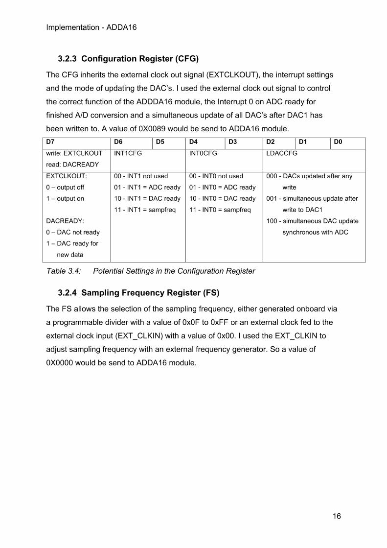
3.2.3 Configuration Register (CFG)
The CFG inherits the external clock out signal (EXTCLKOUT), the interrupt settings
and the mode of updating the DAC’s. I used the external clock out signal to control
the correct function of the ADDDA16 module, the Interrupt 0 on ADC ready for
finished A/D conversion and a simultaneous update of all DAC’s after DAC1 has
been written to. A value of 0X0089 would be send to ADDA16 module. D7 D6 D5 D4 D3 D2 D1 D0
write: EXTCLKOUT
read: DACREADY
INT1CFG INT0CFG LDACCFG
EXTCLKOUT:
0 – output off
1 – output on
DACREADY:
0 – DAC not ready
1 – DAC ready for
new data
00 - INT1 not used
01 - INT1 = ADC ready
10 - INT1 = DAC ready
11 - INT1 = sampfreq
00 - INT0 not used
01 - INT0 = ADC ready
10 - INT0 = DAC ready
11 - INT0 = sampfreq
000 - DACs updated after any
write
001 - simultaneous update after
write to DAC1
100 - simultaneous DAC update
synchronous with ADC
Table 3.4: Potential Settings in the Configuration Register
3.2.4 Sampling Frequency Register (FS)
The FS allows the selection of the sampling frequency, either generated onboard via
a programmable divider with a value of 0x0F to 0xFF or an external clock fed to the
external clock input (EXT_CLKIN) with a value of 0x00. I used the EXT_CLKIN to
adjust sampling frequency with an external frequency generator. So a value of
0X0000 would be send to ADDA16 module.
Implementation - DSP
17
3.2.5 Bus Interface
For a correct function of the ADDA16 following signals would be needed: Signal Pin Type Description
A0 .. A5
A16 .. A18
U9 .. U14
V12 .. V14
I Address bus
D0 .. D15 U15 .. U30 I/O/Z Data bus (connects to DSP D16..D31)
nRD U2 I Active low read strobe signal
nWR U5 I Active low write strobe signal
nIOSEL U8 I Active low memory select signal
BUSCLK U6 I DSP bus clock
NINTO U3 O/Z Interrupt Line 0
nINT1 U4 O/Z Interrupt Line 1
Table 3.5: Pin Connection
Remark Each signal must be connected, except the interrupt signals otherwise the ADDA16
module wouldn’t interpret any command correctly.
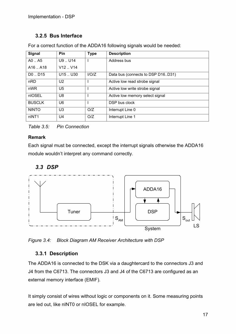
3.3 DSP
TunerSAM Sout
LSSystem
ADDA16
DSP
Figure 3.4: Block Diagram AM Receiver Architecture with DSP
3.3.1 Description
The ADDA16 is connected to the DSK via a daughtercard to the connectors J3 and
J4 from the C6713. The connectors J3 and J4 of the C6713 are configured as an
external memory interface (EMIF).
It simply consist of wires without logic or components on it. Some measuring points
are led out, like nINT0 or nIOSEL for example.
Implementation - DSP
18
Attention should be paid on the daughtercard detect signal J3(75). It must be
grounded. Otherwise the DSK wouldn’t recognize the daughtercard an the bus-
drivers on the DSK will always be HIGH Z !
3.3.2 Software
The DSP C6713 will recognize the ADDA16 module as an external memory
interface, so most of the implementation is already done, cause EMIF is already
implemented on the Expansion Bus (see also [TI190d] and [TI401f]). Only the
necessary adjustments in the EMIF configuration register should be done.
I want to give a short description of the characteristics of the c-program I’ve written
#define IRQ_EXTPOL (*(volatile unsigned int *) 0x019C0008)
This define instruction maps a hardware register to a variable declaration. It is for a
better handling in the c-program. The IRQ_EXTPOL register defines on which edge
the interrupt would be recognized.
3.3.3 External Memory Interface (EMIF) on C6713
For the correct timing you have to adjust the EMIF settings on the C6713. During a
call with Mr.Klemenz of the company D.SignT, he told me the timing of the EMIF
settings.
Asynchronus timing: write setup 1
Write strobe 2
Write hold 1
Read setup 1
Read strobe 2
Read hold 1
Turn around time 1
Table 3.6: EMIF Timing on C6713
With the settings of Table 3.6 and the EMIF-Calculator from D.SignT Hompage
[DST01] it is very easy to generate the correct value for the control register. The
result of the calculator is 0x10914221.
Implementation - DSP
19
I decided to use the chip enable 3 control register (CE3_CTRL) register for this. It
wasn’t used before by any other projects, so other projects of the HAW wouldn’t be
involved. The memory space starts at address 0x90200000 and with the adjustments
of the ADDA16 module the first value is located at address 0x90300000. (see also.
3.2.2)
3.3.4 Address Decoding
Memory type Memory width Maximum
addressable bytes
per CE space
Address output
on EA [21:2]
Represents
ASRAM X16 2M A[20:1] half word address
Table 3.7: TMS320C621x/C671x Addressable Memory Ranges
Like in Table 3.7 is seen, a half word address is used, cause only 16 bit of the 32 bit
address space is used, so the EA-Address is shifted by one to the internal address.
A closer look at the explicit addresses would make a better view of it.
First we had a look at the original address of the CE3 Space. It begins at 1001 0000 0010 0000 0000 0000 0000 0000 Binary
9 0 2 0 0 0 0 0 Hex
Table 3.8: Address Space of CE3
Cause a half word addressable space is used the address output is shifted by 1.
This result in JPA18 goes to A 20 and JPA17 goes to A19 and JPA16 goes to A18
they were called the bank select bits.
JPA5 goes to A17 and JPA4 goes to A16 and were called the sub bank select bits.
A picture would make a better perception.
Remark: JPA = Jumper for Address decoding it has nothing to do with the
correct place of the address bit !) 1001 0000 0010 0000 0000 0000 0000 0000 Binary
9 0 2 0 0 0 0 0 Hex
Xxx1 00xx JPA18 - JPA16
xx00 JPA5 - JPA4
1001 0000 0011 0000 0000 0000 0000 0000 Binary
9 0 3 0 0 0 0 0 Hex
Table 3.9: Address Mapping with the JPA’s
Implementation - Signal Analyze with Logic Analyzer
20
3.4 Signal Analyze with Logic Analyzer
First of all I had to find out how the signals of the ADDA16 module were driven. So I
connect a logic analyzer to the ADDA16 module and connect it to the DSK. After a
short while it was clear how it works and here are the results.
3.4.1 Generics to the Analyzer Pictures
The first picture (Figure 3.5) shows nearly all-available signals from the ADDA16
module except the BUSCLK signal. Here is a short description for each Signal:
Reset for a proper Operation it must be 1
nINT0 Interrupt line 0 to DSP, active on falling edge
nRD not READ signal (read strobe), active low
nWR not WRITE signal (write strobe), active low
nIOSEL not Input Output SELect signal, active low (DSP memory area select
signal)
A18-A16 part of address bus, 64 K Bank select signal, which is described in
section 3.2.2
A5-A4 part of address bus, 16 Word Sub Bank Select signal, which is
described in section 3.2.2
A3-A0 part of address bus, register select offset which is described in section
3.2.2
D15-D0 data bits

Implementation - Signal Analyze with Logic Analyzer
21
Figure 3.5: Complete Reset Cycle
3.4.2 Reset Cycle
In Figure 3.5 the complete reset cycle is shown.
In the beginning nReset is one. Then it goes to null and after 10 ms back to one. This
is also the minimum time for a reset.
When the reset signal is low, every register in the ADDA16 module is set to his initial
value. The initial value of all registers is null.
Note: the green spikes in nRD and nWR were the auto refresh of the synchronic data
random access memory (SDRAM) and have nothing to do with the initialization of the
ADDA16
3.4.3 Initial Procedure
Figure 3.6: Initial Procedure
The second picture (Figure 3.6) shows the typical initial procedure. After the reset
has stopped, the first thing to do is to write the CFG and the FS Register.
Implementation - Signal Analyze with Logic Analyzer
22
First a write to the CFG register is done. It is located at address 0x4 and the value
0x0000 has been send. Second the value 0x0089 is send to the FS register, which is
located at address 0x5.
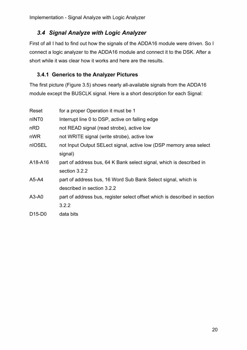
3.4.4 Release of the Interrupt Request Signal nINT0
Figure 3.7: Release of Interrupt
In the picture above (Figure 3.7) the initial is complete. The first ad conversion starts.
If the ad conversion has finished the first interrupt occurs. A falling edge of nINT0 is
created by the ADDA16.
3.4.5 Complete Interrupt Function
Figure 3.8: Complete Interrupt Function
Figure 3.8 shows the complete Interrupt function. I split this picture into 3 parts
because the explicit values aren’t good to be seen.
Implementation - Signal Analyze with Logic Analyzer
23
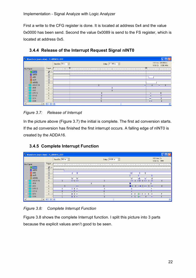
3.4.6 First Part of Interrupt Function
Now we had a closer look after the interrupt occurs.
Figure 3.9: First Part of Interrupt Function
In the ISR the first operation is a read from the two ADC’s.
First ADC0 is read and second ADC1 is read.
3.4.7 Middle Part of Interrupt Function
In the middle of ISR (see Figure 3.10) nothing happened to the output, because the
output value is to be computed.
Figure 3.10: Middle Part of Interrupt Function
3.4.8 Last Part of Interrupt Function
In the Figure 3.11 underneath, is the first thing a read to the CFG register cause a
write to DAC0 is to be made next. This had to be done because the DAC interface is
single-buffered and got only one buffer for all DAC’s.
Implementation - Signal Analyze with Logic Analyzer
24
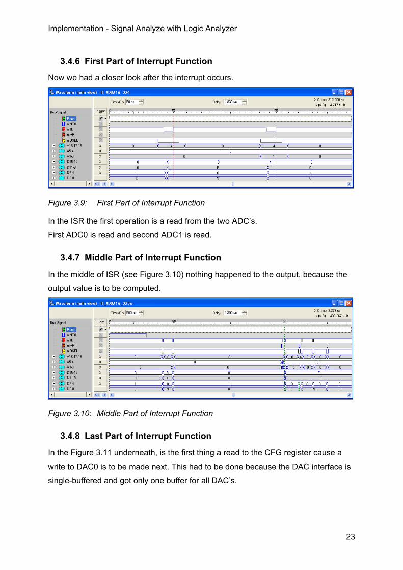
Figure 3.11: Last Part of Interrupt Function
Bit 7 of CFG-register is the DAC_READY signal. If it is 0, the DAC buffer is full and
new data cannot be accepted or in other word’s the shift to the explicit DAC haven’t
finished yet. So you have to wait until the shift had been done (in Figure 3.11 192ns
wait time was estimated) and ask again if it has emptied.
If a 1 is detected, the write to the DAC have finished and the DAC buffer is ready to
accept new data. Another write to an other DAC could be done.
In the Figure 3.11 above this is the first write to a DAC after a long while so bit 7 of
the CFG-register is 1. To be seen on D15 to D0, its value is 0xFF89 so D7 is 1.
After the DAC_READY signal is 1, a write to DAC0 is performed with the value
0xFFFF and immediately afterwards a read of the CFG register, where D7 is 0. So it
was done as I explained it above.
Thereafter DAC1 is written with its value and the ISR is complete.
Now the system is in idle progress until the next falling edge of nINT0 is recognized
and the ISR is called again.
Implementation - Signal Analyze with Logic Analyzer
25
BUSCLK
nRD
nIOSEL
A3-0 0x0 0x4 0x0
1 3 2 5state
4
6
7
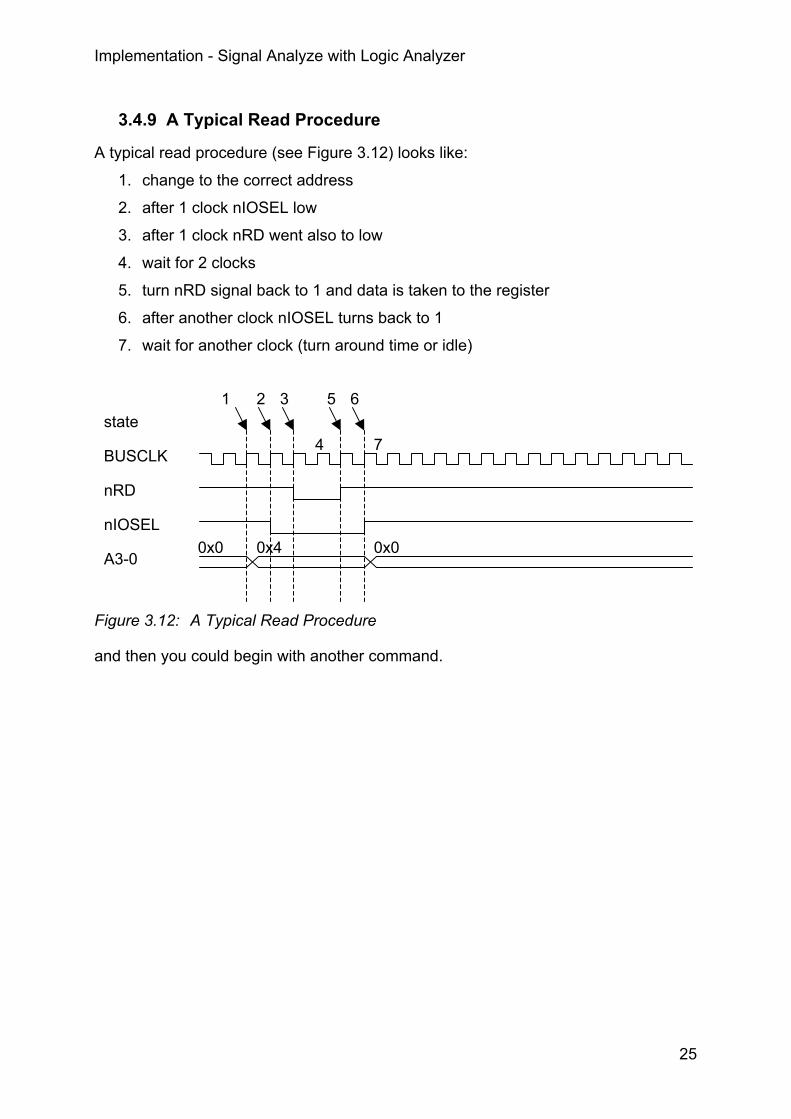
3.4.9 A Typical Read Procedure
A typical read procedure (see Figure 3.12) looks like:
1. change to the correct address
2. after 1 clock nIOSEL low
3. after 1 clock nRD went also to low
4. wait for 2 clocks
5. turn nRD signal back to 1 and data is taken to the register
6. after another clock nIOSEL turns back to 1
7. wait for another clock (turn around time or idle)
Figure 3.12: A Typical Read Procedure
and then you could begin with another command.
Implementation - Signal Analyze with Logic Analyzer
26
BUSCLK
nWR
nIOSEL
A3-0 0x0 0x4 0x0
1 3 2 5state
4
6
7
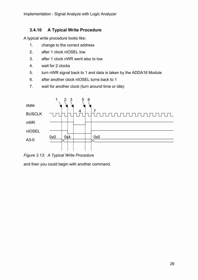
3.4.10 A Typical Write Procedure
A typical write procedure looks like:
1. change to the correct address
2. after 1 clock nIOSEL low
3. after 1 clock nWR went also to low
4. wait for 2 clocks
5. turn nWR signal back to 1 and data is taken by the ADDA16 Module
6. after another clock nIOSEL turns back to 1
7. wait for another clock (turn around time or idle)
Figure 3.13: A Typical Write Procedure
and then you could begin with another command.
Implementation - FPGA with Xilinx MicroBlaze
27
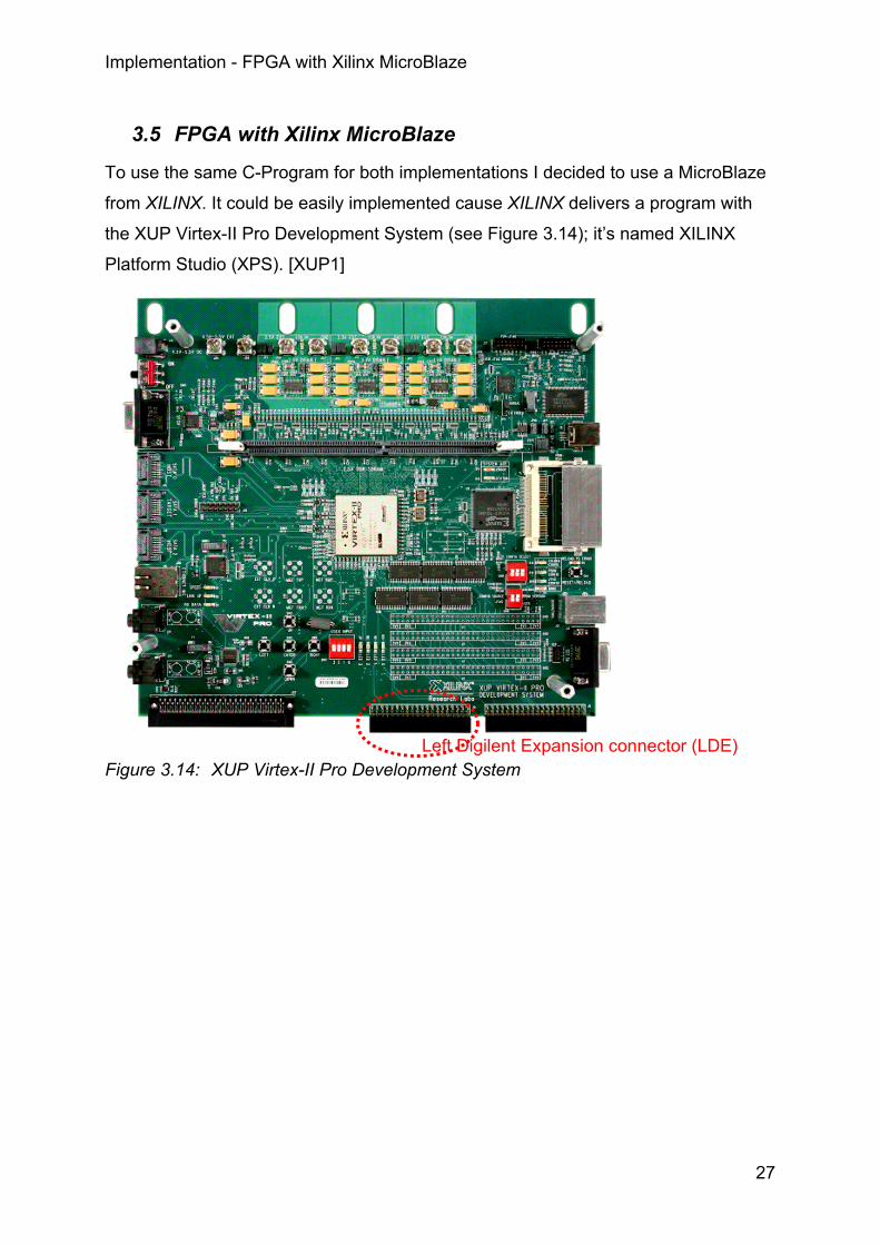
3.5 FPGA with Xilinx MicroBlaze
To use the same C-Program for both implementations I decided to use a MicroBlaze
from XILINX. It could be easily implemented cause XILINX delivers a program with
the XUP Virtex-II Pro Development System (see Figure 3.14); it’s named XILINX
Platform Studio (XPS). [XUP1]
Figure 3.14: XUP Virtex-II Pro Development System Left Digilent Expansion connector (LDE)
Implementation - FPGA with Xilinx MicroBlaze
28
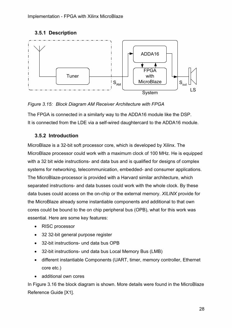
3.5.1 Description
TunerSAM Sout
LSSystem
ADDA16
FPGAwith
MicroBlaze
Figure 3.15: Block Diagram AM Receiver Architecture with FPGA
The FPGA is connected in a similarly way to the ADDA16 module like the DSP.
It is connected from the LDE via a self-wired daughtercard to the ADDA16 module.
3.5.2 Introduction
MicroBlaze is a 32-bit soft processor core, which is developed by Xilinx. The
MicroBlaze processor could work with a maximum clock of 100 MHz. He is equipped
with a 32 bit wide instructions- and data bus and is qualified for designs of complex
systems for networking, telecommunication, embedded- and consumer applications.
The MicroBlaze-processor is provided with a Harvard similar architecture, which
separated instructions- and data busses could work with the whole clock. By these
data buses could access on the on-chip or the external memory. XILINX provide for
the MicroBlaze already some instantiable components and additional to that own
cores could be bound to the on chip peripheral bus (OPB), what for this work was
essential. Here are some key features:
• RISC processor
• 32 32-bit general purpose register
• 32-bit instructions- und data bus OPB
• 32-bit instructions- und data bus Local Memory Bus (LMB)
• different instantiable Components (UART, timer, memory controller, Ethernet
core etc.)
• additional own cores
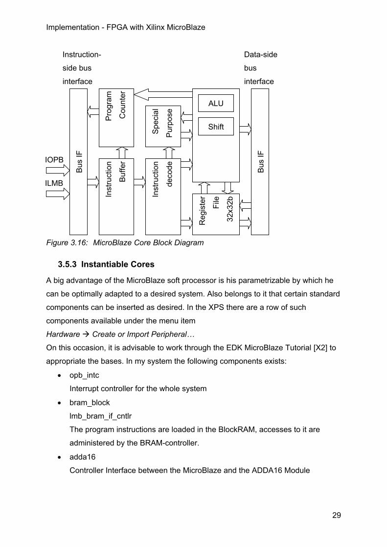
In Figure 3.16 the block diagram is shown. More details were found in the MicroBlaze
Reference Guide [X1].
Implementation - FPGA with Xilinx MicroBlaze
29
Figure 3.16: MicroBlaze Core Block Diagram
3.5.3 Instantiable Cores
A big advantage of the MicroBlaze soft processor is his parametrizable by which he
can be optimally adapted to a desired system. Also belongs to it that certain standard
components can be inserted as desired. In the XPS there are a row of such
components available under the menu item
Hardware Create or Import Peripheral…
On this occasion, it is advisable to work through the EDK MicroBlaze Tutorial [X2] to
appropriate the bases. In my system the following components exists:
• opb_intc
Interrupt controller for the whole system
• bram_block
lmb_bram_if_cntlr
The program instructions are loaded in the BlockRAM, accesses to it are
administered by the BRAM-controller.
• adda16
Controller Interface between the MicroBlaze and the ADDA16 Module
Instruction-
side bus
interface
ILMB
IOPB In
stru
ctio
n
deco
de
Reg
iste
r
File
32x3
2b
Data-side
bus
interface
ALU
Shift
Inst
ruct
ion
Buf
fer
Pro
gram
Cou
nter
Spe
cial
Pur
pose
Bus
IF
Bus
IF
Implementation - FPGA with Xilinx MicroBlaze
30
3.5.4 Interrupt Controller
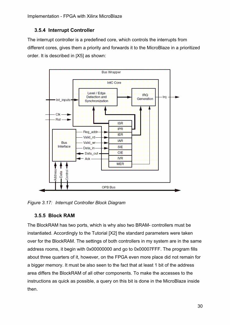
The interrupt controller is a predefined core, which controls the interrupts from
different cores, gives them a priority and forwards it to the MicroBlaze in a prioritized
order. It is described in [X5] as shown:
Figure 3.17: Interrupt Controller Block Diagram
3.5.5 Block RAM
The BlockRAM has two ports, which is why also two BRAM- controllers must be
instantiated. Accordingly to the Tutorial [X2] the standard parameters were taken
over for the BlockRAM. The settings of both controllers in my system are in the same
address rooms, it begin with 0x00000000 and go to 0x00007FFF. The program fills
about three quarters of it, however, on the FPGA even more place did not remain for
a bigger memory. It must be also seen to the fact that at least 1 bit of the address
area differs the BlockRAM of all other components. To make the accesses to the
instructions as quick as possible, a query on this bit is done in the MicroBlaze inside
then.
Implementation - FPGA with Xilinx MicroBlaze
31
3.5.6 Own Core
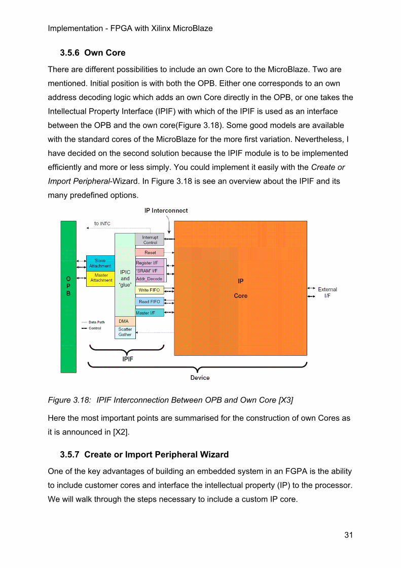
There are different possibilities to include an own Core to the MicroBlaze. Two are
mentioned. Initial position is with both the OPB. Either one corresponds to an own
address decoding logic which adds an own Core directly in the OPB, or one takes the
Intellectual Property Interface (IPIF) with which of the IPIF is used as an interface
between the OPB and the own core(Figure 3.18). Some good models are available
with the standard cores of the MicroBlaze for the more first variation. Nevertheless, I
have decided on the second solution because the IPIF module is to be implemented
efficiently and more or less simply. You could implement it easily with the Create or
Import Peripheral-Wizard. In Figure 3.18 is see an overview about the IPIF and its
many predefined options.
Figure 3.18: IPIF Interconnection Between OPB and Own Core [X3]
Here the most important points are summarised for the construction of own Cores as
it is announced in [X2].
3.5.7 Create or Import Peripheral Wizard
One of the key advantages of building an embedded system in an FGPA is the ability
to include customer cores and interface the intellectual property (IP) to the processor.
We will walk through the steps necessary to include a custom IP core.
Implementation - FPGA with Xilinx MicroBlaze
32
• In XPS, select Hardware → Create or Import Peripheral… to open the Create
and Import Peripheral Wizard.
• Click Next. Select Create templates for a new peripheral.
By default the new peripheral will be stored in the project_directory/pcores
directory. This enables XPS to find the core for utilization during the
embedded system development.
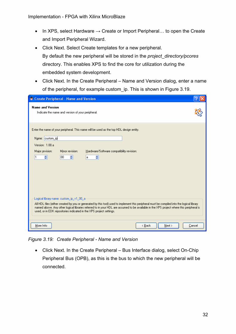
• Click Next. In the Create Peripheral – Name and Version dialog, enter a name
of the peripheral, for example custom_ip. This is shown in Figure 3.19.
Figure 3.19: Create Peripheral - Name and Version
• Click Next. In the Create Peripheral – Bus Interface dialog, select On-Chip
Peripheral Bus (OPB), as this is the bus to which the new peripheral will be
connected.
Implementation - FPGA with Xilinx MicroBlaze
33
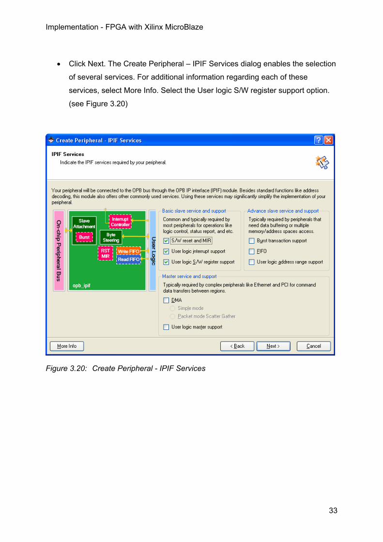
• Click Next. The Create Peripheral – IPIF Services dialog enables the selection
of several services. For additional information regarding each of these
services, select More Info. Select the User logic S/W register support option.
(see Figure 3.20)
Figure 3.20: Create Peripheral - IPIF Services
Implementation - FPGA with Xilinx MicroBlaze
34
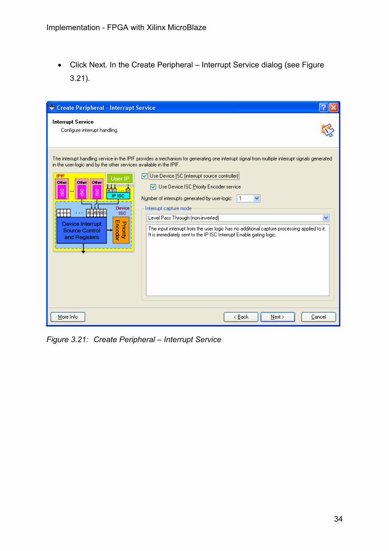
• Click Next. In the Create Peripheral – Interrupt Service dialog (see Figure
3.21).
Figure 3.21: Create Peripheral – Interrupt Service
Implementation - FPGA with Xilinx MicroBlaze
35
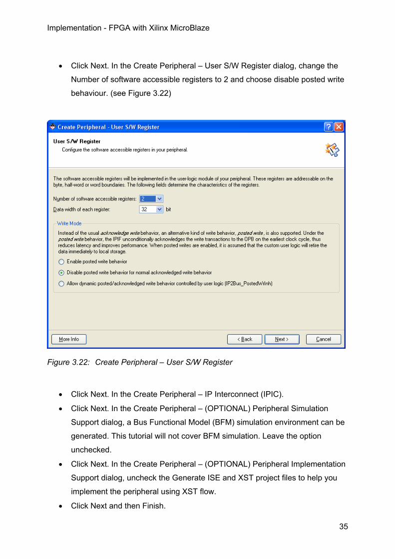
• Click Next. In the Create Peripheral – User S/W Register dialog, change the
Number of software accessible registers to 2 and choose disable posted write
behaviour. (see Figure 3.22)
Figure 3.22: Create Peripheral – User S/W Register
• Click Next. In the Create Peripheral – IP Interconnect (IPIC).
• Click Next. In the Create Peripheral – (OPTIONAL) Peripheral Simulation
Support dialog, a Bus Functional Model (BFM) simulation environment can be
generated. This tutorial will not cover BFM simulation. Leave the option
unchecked.
• Click Next. In the Create Peripheral – (OPTIONAL) Peripheral Implementation
Support dialog, uncheck the Generate ISE and XST project files to help you
implement the peripheral using XST flow.
• Click Next and then Finish.
Implementation - FPGA with Xilinx MicroBlaze
36
Now that the template has been created, the user_logic.vhd file must be modified to
incorporate the custom IP functionality.
• Open the user_logic.vhd in windows explorer. Currently the code provides an
example of reading and writing to two 32-bit registers and a primitive interrupt.
3.5.8 Microprocessor Peripheral Definition (MPD)
Each system peripheral has a corresponding MPD file. The MPD file is the symbol of
the embedded system peripheral to the MHS schematic of the embedded system.
The MPD file contains all of the available ports and hardware parameters for a
peripheral. These ports are also performed in the XPS. First the name of own cores
is given again:
BEGIN my_core_name, IPTYPE = PERIPHERAL, EDIF= TRUE
Under this name an own core will appear in the XPS. Then the ports must be
defined. Here an example:
PORT name = "", DIR = IN, VEC[0:15]
DIR defines whether a port is an input or an output. If a port is fixed as DIR = INOUT,
this can lead while generating the net list to mistakes, if is not added, in addition,
ENABLE=MULTI. Then this looks thus:
PORT name = "", DIR = INOUT, VEC[0:15], ENABLE=MULTI
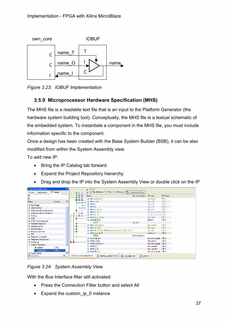
ENABLE=MULTI get XPS an IOBUF after Figure 3.23 to provide. With the very high
speed integrated circuit hardware description language (VHDL) files adaptations
must be likewise done, so that an input output buffer (IOBUF) is properly inserted.
From the port name there were three ports automatically added:
• name_I as an input for the own core
• name_O as an output for the own core
• name_T to activate the tri-state signal (active low)
Implementation - FPGA with Xilinx MicroBlaze
37
Figure 3.23: IOBUF Implementation
3.5.9 Microprocessor Hardware Specification (MHS)
The MHS file is a readable text file that is an input to the Platform Generator (the
hardware system building tool). Conceptually, the MHS file is a textual schematic of
the embedded system. To instantiate a component in the MHS file, you must include
information specific to the component.
Once a design has been created with the Base System Builder (BSB), it can be also
modified from within the System Assembly view.
To add new IP:
• Bring the IP Catalog tab forward.
• Expand the Project Repository hierarchy
• Drag and drop the IP into the System Assembly View or double click on the IP
Figure 3.24: System Assembly View
With the Bus Interface filter still activated:
• Press the Connection Filter button and select All
• Expand the custom_ip_0 instance
own_core
name_I
name name_O
name_T
IOBUF
O
O
I
T
I
O
Implementation - FPGA with Xilinx MicroBlaze
38
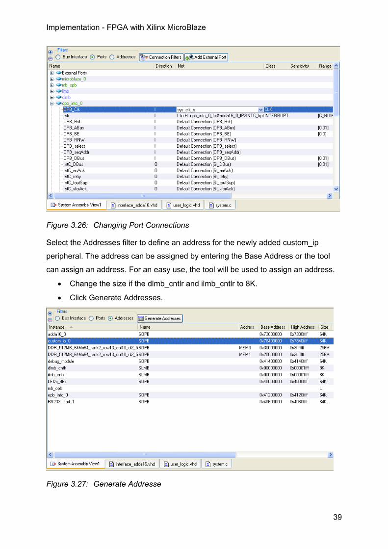
• Highlite the slave OPB connection (SOPB)
• Select the No Connection pull down menu and change it to mb_opb
Figure 3.25: Modyfing Bus Connections
Now select the Ports filter
• Press the Connection Filter button and select All
• Expand the custom_ip_0 instance
• Highlite the OPB_Clk port
• Select the Default Connection pull down menu and change the clock
connection to sys_clk_s
Implementation - FPGA with Xilinx MicroBlaze
39
Figure 3.26: Changing Port Connections
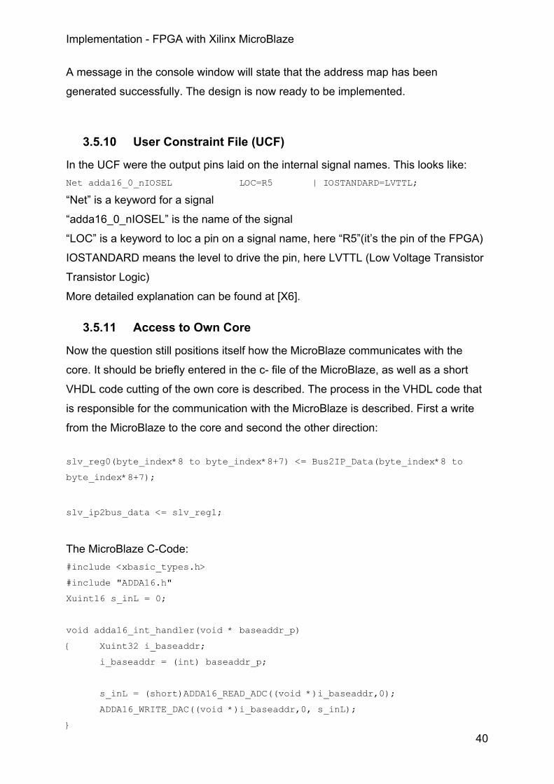
Select the Addresses filter to define an address for the newly added custom_ip
peripheral. The address can be assigned by entering the Base Address or the tool
can assign an address. For an easy use, the tool will be used to assign an address.
• Change the size if the dlmb_cntlr and ilmb_cntlr to 8K.
• Click Generate Addresses.
Figure 3.27: Generate Addresse
Implementation - FPGA with Xilinx MicroBlaze
40
A message in the console window will state that the address map has been
generated successfully. The design is now ready to be implemented.
3.5.10 User Constraint File (UCF)
In the UCF were the output pins laid on the internal signal names. This looks like: Net adda16_0_nIOSEL LOC=R5 | IOSTANDARD=LVTTL;
“Net” is a keyword for a signal
“adda16_0_nIOSEL” is the name of the signal
“LOC” is a keyword to loc a pin on a signal name, here “R5”(it’s the pin of the FPGA)
IOSTANDARD means the level to drive the pin, here LVTTL (Low Voltage Transistor
Transistor Logic)
More detailed explanation can be found at [X6].
3.5.11 Access to Own Core
Now the question still positions itself how the MicroBlaze communicates with the
core. It should be briefly entered in the c- file of the MicroBlaze, as well as a short
VHDL code cutting of the own core is described. The process in the VHDL code that
is responsible for the communication with the MicroBlaze is described. First a write
from the MicroBlaze to the core and second the other direction:
slv_reg0(byte_index*8 to byte_index*8+7) <= Bus2IP_Data(byte_index*8 to
byte_index*8+7);
slv_ip2bus_data <= slv_reg1;
The MicroBlaze C-Code: #include <xbasic_types.h>
#include "ADDA16.h"
Xuint16 s_inL = 0;
void adda16_int_handler(void * baseaddr_p)
{ Xuint32 i_baseaddr;
i_baseaddr = (int) baseaddr_p;
s_inL = (short)ADDA16_READ_ADC((void *)i_baseaddr,0);
ADDA16_WRITE_DAC((void *)i_baseaddr,0, s_inL);
}
Implementation - FPGA with Xilinx MicroBlaze
41
In the C- code the h-files are inserted first: xbasic_types.h contains the base types
definitions. Thus is, for example, Xuint32 nothing other than an unsigned long
variable, i.e. 32 bit-wide. For the access to the own core it is very important to include
adda16.c and adda16.h. There functions defined like ADDA16_WRITE_DAC with
XIo_Out32 and ADDA16_READ_ADC with XIo_In32. For ADDA16_WRITE_DAC
following data would be needed: the address pointer i_baseaddr, the port 0 and a 16
bit-wide data word. The data is send from the MicroBlaze over the OPB to the own
core. If the data arrives in the own core, Bus2IP_CS and Bus2IP_WrCE got one, and
Bus2IP_Data passes on the data in slv_reg0. Vice versa the data of IP2Bus_Data
comes with ADDA16_READ_ADC and is, in the end, in the variable s_inL.
3.5.12 User Logic from Own Core
For a correct function of the interconnection with the ADDA16 Module I had to write
the half of the user logic and the complete adda16.vhd files. As it is described in the
section before, the MicroBlaze could send and receive 32-bit wide data words
between the C- code and the own core. But there is some more originality that must
be described.
First I had the Problem that the correct data isn’t being received in the
user_logic.vhd. For this is the answer a little bit complicated to understand. In the
Crate and import Peripheral -Wizard is a page where one can control the
acknowledge behavior of the own core for the data word. I’ve chosen the write
acknowledge behavior, so the C-code could receive a data word from the ADDA16
module, after a request to the own core was send and wait for its answer. The correct
data is primal available after 5 clocks. The data between the MicroBlaze and the own
core is sending in 8-bit wide pieces. So I developed a counter, which counts up to
five and stops after it. Here is the code example for this problem:
Note: The slv_ack_detect signal is only for one clock high, after a write to the user-
logic had begun. wait_5_clocks:process(Bus2IP_Clk)
begin
if Bus2IP_Clk='1' and Bus2IP_Clk'event then
if (slv_ack_detect = '1') then
count_5 <= "001";
else
case (count_5) is
when "001" =>
Implementation - FPGA with Xilinx MicroBlaze
42
count_5 <= "010";
when "010" =>
count_5 <= "011";
when "011" =>
count_5 <= "100";
when "100" =>
count_5 <= "101";
when "101" =>
count_5 <= "110";
when others => null;
end case;
end if;
end if;
end process wait_5_clocks;
finish_write_from_UL <= '1' when count_5 = "101" else '0';
After that I had the problem how to interact with the own core and the MicroBlaze, so
it could be done with two Interrupts either, but this isn’t easy to implement, cause
only one interrupt comes from the own core and after the ISR is started you have to
ask in the IPIF of the own core, which interrupt occurred. So I decided to use only
one Interrupt and the system had to wait for the correct answer about 10 clocks.
Another advantage is a faster system then two interrupts occur.
But if you have to wait more then 7 clocks, you have to implement a timeout signal.
The timeout signal is generated in an own process: Timeout_process: process (Bus2IP_Clk, Bus2IP_Reset, slv_ack_detect)
begin
if (Bus2IP_Reset = '1') or (slv_ack_detect = '1') then
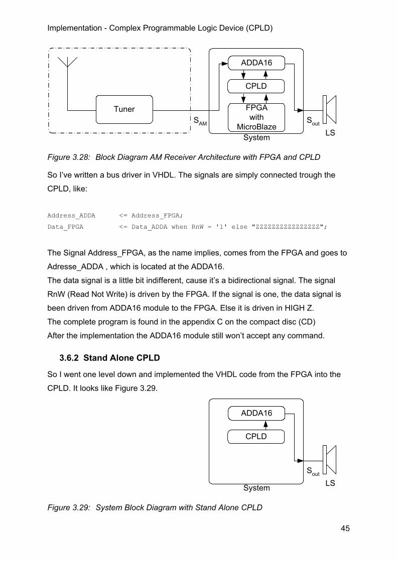
timeout <= (others => '0');
elsif Bus2IP_Clk='1' and Bus2IP_Clk'event then
timeout <= timeout + 1;
end if;
end process Timeout_process;
IP2Bus_ToutSup <= not timeout(26);--'0';-- Timeout after 1,34sec
3.5.13 Interface from Own Core
The communication between the own core and the ADDA16 Module is described in
the interface_adda16.vhdl. Hence which is a component of the user_logic.vhd, so it is
instantiated in the same. The ports would cross by port mapping to the component.
The component is programmed in standard VHDL. I decided to program a MOORE
Implementation - FPGA with Xilinx MicroBlaze
43
state machine, cause the output signals have nothing directly to do with the input
signals, so no MEALY state machine is needed. An advantage of a Moore state
machine is the easily changeability, like the signals and states or its regularity, a
disadvantage is its slowly ness and the place requirements in its implementation, but
it fits best of all.
A short explanation to the single segments of the program code is following:
For a better reading I named the states with a personal name, here an example:
type state_type is (st0_initial_state, st1_reset);
signal state, next_state : state_type;
As it was seen above I declared a new type, named the elements of the new type
and subsequently defined a signal, which is from the predefined new type. The
advantage is obvious clearly, the named types simplifies the reading of the source
code and therefore also understanding tremendously and the pre-compiler replace it
with a series of numbers, a disadvantage are the longer name definitions by which
this program becomes a little bit complex.
To force a reading of the BUSCLK signal the following code lines were implemented:
Internal_CLK:
CLKintern <= Bus2IP_Clk ;
BUSCLK <= CLKintern ;
The “Internal_CLK:” is an identifier for the program and Bus2IP_Clk is the clock
signal from the FPGA, it runs at 100MHz and BUSCLK is the signal that goes to the
ADDA16 module, it runs also at 100MHz.
In the process “SYNC_PROC:“ are laid all internal signal on external ones, if it’s a rising
edge of the CLKintern signal; it is also defined what happens with the signals if the
reset signal (Bus2IP_Reset) is released.
The process “INPUT_DECODE:” synchronizes the slave registers from the user_logic to
the component. After a data word is received from the C- code of the MicroBlaze to
the core it is recognized here and the MOORE state machine knows what to do.
Implementation - Complex Programmable Logic Device (CPLD)
44
In a MOORE state machine all outputs were based on the internal state only and this
happens in the “OUTPUT_DECODE:” process, like nRESET, nRD, nWR or other signals,
that goes to the ADDA16 module.
The last process is the “NEXT_STATE_DECODE:” process, where all state changes take
place.
3.5.14 Address Decoding
For updating the valid address as soon as possible, the address lines A3-A0 are
updated without the state machine, it looks like:
Address_i <= slv_reg0_i(19 downto 16);
So that the address is updated immediately after a new valid data has been taken
from the user_logic to the interface.
By the Time JPA18 to JPA16, JPA5 and JPA4 weren’t connected, cause the signals
are pulled inside the ADDA16 module by the jumpers on a defined potential, on
account of that to the FPGA.
3.6 Complex Programmable Logic Device (CPLD)
After I implemented everything on the FPGA, the ADDA16 module didn’t understand
anything, so I decided to have a closer look at the output values that were driven by
the FPGA. They were nearly out of spec of the ADDA16 module (according to Mr
Klemenz from DsignT). So I implemented a bus driver via a CPLD.
3.6.1 Bus Driver with CPLD
The CPLD got a great advantage, cause it could be driven with two voltage- levels,
one for the input and another one for the output. A great disadvantage is the work
behind that all, the programming, the production of another daughtercard, the
implementation. But to act fast, it was the best implementation I could get in time.
Implementation - Complex Programmable Logic Device (CPLD)
45
TunerSAM Sout
LSSystem
ADDA16
FPGAwith
MicroBlaze
CPLD
Figure 3.28: Block Diagram AM Receiver Architecture with FPGA and CPLD
So I’ve written a bus driver in VHDL. The signals are simply connected trough the
CPLD, like:
Address_ADDA <= Address_FPGA;
Data_FPGA <= Data_ADDA when RnW = '1' else "ZZZZZZZZZZZZZZZZ";
The Signal Address_FPGA, as the name implies, comes from the FPGA and goes to
Adresse_ADDA , which is located at the ADDA16.
The data signal is a little bit indifferent, cause it’s a bidirectional signal. The signal
RnW (Read Not Write) is driven by the FPGA. If the signal is one, the data signal is
been driven from ADDA16 module to the FPGA. Else it is driven in HIGH Z.
The complete program is found in the appendix C on the compact disc (CD)
After the implementation the ADDA16 module still won’t accept any command.
3.6.2 Stand Alone CPLD
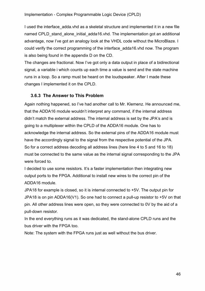
So I went one level down and implemented the VHDL code from the FPGA into the
CPLD. It looks like Figure 3.29.
Sout
LSSystem
ADDA16
CPLD
Figure 3.29: System Block Diagram with Stand Alone CPLD
Implementation - Complex Programmable Logic Device (CPLD)
46
I used the interface_adda.vhd as a skeletal structure and implemented it in a new file
named CPLD_stand_alone_initial_adda16.vhd. The implementation got an additional
advantage, now I’ve got an analogy look at the VHDL code without the MicroBlaze. I
could verify the correct programming of the interface_adda16.vhd now. The program
is also being found in the appendix D on the CD.
The changes are fractional. Now I’ve got only a data output in place of a bidirectional
signal, a variable i which counts up each time a value is send and the state machine
runs in a loop. So a ramp must be heard on the loudspeaker. After I made these
changes I implemented it on the CPLD.
3.6.3 The Answer to This Problem
Again nothing happened, so I’ve had another call to Mr. Klemenz. He announced me,
that the ADDA16 module wouldn’t interpret any command, if the internal address
didn’t match the external address. The internal address is set by the JPA’s and is
going to a multiplexer within the CPLD of the ADDA16 module. One has to
acknowledge the internal address. So the external pins of the ADDA16 module must
have the accordingly signal to the signal from the respective potential of the JPA.
So for a correct address decoding all address lines (here line 4 to 5 and 16 to 18)
must be connected to the same value as the internal signal corresponding to the JPA
were forced to.
I decided to use some resistors. It’s a faster implementation then integrating new
output ports to the FPGA. Additional to install new wires to the correct pin of the
ADDA16 module.
JPA18 for example is closed, so it is internal connected to +5V. The output pin for
JPA18 is on pin ADDA16(V1). So one had to connect a pull-up resistor to +5V on that
pin. All other address lines were open, so they were connected to 0V by the aid of a
pull-down resistor.
In the end everything runs as it was dedicated, the stand-alone CPLD runs and the
bus driver with the FPGA too.
Note: The system with the FPGA runs just as well without the bus driver.
Comparison of Both Implementations - Complex Programmable Logic Device (CPLD)
47
4 Comparison of Both Implementations The program of the DSP explained in section 3.3.2 is compiled with the different
optimization levels of the compiler. The DSP runs also with different clock cycles to
get a better comparison of both implementations, if they run with the same clock
cycle. After each optimization and speed level is performed the program is
downloaded to the DSK and measured with the logic analyzer. The FPGA runs
always at 100 MHz and runs with optimization level -7
frequency -o0 -o1 -02 -o3
225MHz 2.756µs 2.484µs 2.476µs 2.476µs
100MHz 4.952µs 4.376µs 4.324µs 4.324µs
Table 4.1: Comparison of optimization levels
As in Table 4.1 seen, the optimization level does speed up the ISR. The DSP has
enough potential for demodulation the AM signal.
On the other hand the FPGA needs about 72µs for a demodulation calculation. So
this results in a maximum sampling frequency of 13.88kHz. A sampling frequency of
140 kHz is being needed, so the FPGA isn’t qualified for the demodulation. The
pictures and possible solutions would be found in appendix E on the CD.
Conclusions and Recommendations - Complex Programmable Logic Device (CPLD)
48
5 Conclusions and Recommendations After the last months I could reply on two systems, which convert an analog value to
a digital value via the DAC of the ADDA16 module, store the values in a variable and
push them to the demodulator algorithm to calculate a valid output value. Afterwards
the calculated output value would be send to the DAC of the ADDA16 module and be
heard on a loudspeaker.
First the ADDA16 module was adapted to the DSP in this diploma thesis. Its signals
analyzed and implemented on an FPGA after that. So myself programmed a primitive
EMIF controller.
In a future work maybe the communication to the ADDA16 module could be further
optimized or a better algorithm for the demodulation could be developed and
implemented on the FPGA for example. The result of the FPGA could be more
efficient if a newer and so driven with a higher clock frequency. Maybe the
demodulation could be implemented complete in hardware but this is guesswork and
has to be evaluated for giving a qualified answer.
A printed daughtercard (i.e. with a layout program like EAGLE) for the FPGA or the
CPLD would increase the noise interferences.
49
A. Abbreviations A/D Analog-to-Digital
ADC Analog-to-Digital converter
ADDA16 module D.Module.ADDA16 from DsignT
AM Amplitude Modulation
ASRAM asynchronous random access memory
BSB Base System Builder
BUSCLK bus clock
CD compact disc
CE3 chip enable 3 signal
CE3_CTRL chip enable 3 control register
CFG Configuration Register
CPLD Complex Programmable Logic Device
D/A Digital-to-Analog
DAC Digital-to-Analog converter
DSK DSP Starter Kit
DSP Digital Signal Processor
EA-Address internal identifier of TI
EMIF external memory interface
EXT_CLKIN external clock input
EXTCLKOUT external clock out signal
FS Sampling Frequency Register
fT carrier frequency
HAW University of applied sciences Hamburg
IF intermediate frequency
INTxCFG Configuration of interrupt x
IOBUF input output buffer
IOSEL Input Output SELect
IP intellectual property
IPIF Intellectual Property Interface
ISR Interrupt Service Routine
JPA Jumper for Address decoding
LDACCFG update configuration register for the DAC
50
LDE Left Digilent Expansion connector
LS Loud Speaker
LVTTL Low Voltage Transistor Transistor Logic
MHS Microprocessor Hardware Specification
MicroBlaze soft processor core
MPD Microprocessor Peripheral Definition
nIOSEL not IOSEL
nRD not Read
nWR not Write
OPB Local Memory Bus
OPB on chip peripheral bus
RF Radio Frequency
RISC reduced instruction set computing
RnW Read Not Write
sAM Amplitude modulated Signal
SAR Successive Approximation Converters
SDRAM synchronic data random access memory
sout out signal to Speaker
TI Texas Instruments
UCF User Constraint File
VHDL Very High Speed Integrated Circuit Hardware Description
Language
XPS XILINX Platform Studio
51
B. Bibliography [GK93] P.Gerdsen and P.Kröger, Digitale Signalverarbeitung in der
Nachrichtenübertragung, Springer-Verlag Berlin Heidelberg 1993
[KK02] K. D. Kammeyer and K. Kroschel, Digitale Signalverarbeitung,
B.G.Teubner, Stuttgart 11.2002, page 265
[HL04] E. Herther, W. Lörcher, Nachrichtentechnik, Hanser Verlag, München
Wien 2004, page 321 to 327
[X1] Xilinx, MicroBlaze Processor Reference Guide for Embedded
Development Kit (EDK),
http://www.xilinx.com/ise/embedded/mb_ref_guide.pdf,
30.06.2007 16:32
[X2] EDK 8.2 MicroBlaze Tutorial in Spartan 3
ftp://www.xilinx.com/support/techsup/tutorials/EDK_82_MB_Tutorial.pdf
30.06.2007 16:37
[X3] opb_ipif page 3
http://www.xilinx.com/ipcenter/catalog/logicore/docs/opb_ipif.pdf
01.07.2007 23:59
[X4] user_core_templates_ref_guide
http://japan.xilinx.com/ise/embedded/edk6_2docs/user_core_templates
_ref_guide.pdf
02.07.2007 14:31
[X5] OPB Interrupt Controller (v1.00c)
http://www.xilinx.com/bvdocs/ipcenter/data_sheet/opb_intc.pdf
02.07.2007 18:50
[X6] UCF File Specifications
http://toolbox.xilinx.com/docsan/xilinx4/data/docs/cgd/entry7.html
02.07.2007 20:20
[XUP1] XUP Virtex-II Pro Development System,Hardware Reference Manual
http://www.stanford.edu/class/ee108b/labs/ug069.pdf
02.07.2007 19:15
[DST04] D.Module.ADDA16.pdf Version: Doc #1.0
[DST01] TMS320C6000 EMIF Calculator
http://www.dsignt.de/support/tools/c6000emif.html
52
01.07.2007 15:30
[SIG1] Classification of emissions and necessary bandwidths
http://life.itu.int/radioclub/rr/ap01.htm
03.07.2007 00:42
[TI190d] TMS320C6000 Peripherals Reference Guide
SPRU190d.pdf, chapter 8 Expansion BUS and chapter 10 EMIF
[TI401f] TMS320C6000 Chip Support Library API User’s Guide
SPRU401f.pdf, chapter 9 EMIF Modul
[TI67] TMS320C6713 FLOATING-POINT DIGITAL SIGNAL PROCESSOR
SPRS186B – DECEMBER 2001, page 1
53
Versicherung über die Selbstständigkeit
Hiermit versichere ich, dass ich die vorliegende Arbeit im Sinne der Prüfungsordnung
nach §25(4) ohne fremde Hilfe selbstständig verfasst habe und nur die angegebenen
Hilfsmittel benutzt habe.
Ort, Datum Unterschrift