Embed Size (px)
Citation preview
DRL No. 176 ORO No. MA-8
FINAL REPORT
DOE/ J PL/956254-2 (DE84010981 )
Distribution Category UC-63b
Diodes in Photovoltaic Modules and Arrays
Prepared Under JPL Contract 956254
N.F. Shepard. Jr., Program Manager
The JPL Flat-Plate Solar Array Project is sponsored by the U.S. Department of Energy and forms part of the Solar Photovoltalc Conversion Program to initiate a major ~fort toward the development of flat-plate solar arrays. This work was performed for the Jet Propulsion Laboratory. California Institute of Technology by agreement between NASA and DOE.
GENERAL" ELECTRIC ADVANCED ENERGY PROGRAMS DEPARTMENT
P.o. Box 527 King of Prussia, PA 19406
REPRODUCED BY, NJ'lI u.s. Department of Commerce
National Technicallnformalion Service Springfield, Virginia 22161
ACKNOWLEDGEMENT
The following General Electric Company employees have made significant contributions to the content of this study in the areas indicated.
N.F. Shepard, Jr.
R. W. Drummond
D.M. Mullings
Program Manager and Principal Technical Contributor
Design of Diode Enclosures
Diode Enclosure Costing Analysis
Mr. R.S. Sugimura was the JPL Project Manager. His guidance and helpful suggestions are gratefully acknowledged.
i i
ABSTRACT
The use of diodes to enhance the energy generation capability ana improve the reliability of photovoltaic modules and arrays is the subject of this final report. Beginning with a discussion of the array-level considerations influencing the application of such diodes in a bypass mode, the report continues further to describe several methods for the mechanical and electrical integration of these devices as an integral part of the module electrical termination means. Particular emphasis is placed on the description of innovative approaches for the external mounting of bypass diodes. These descriptions were used as the basis for a detailed cost analysis and comparison among the candidate concepts.
The photovoltaic source circuit blocking or isolation function can be implemented using the same basic diode enclosure designs with provisions for the inclusion ofa fuse for overcurrent protection.
iii

TABLE OF CONTENTS
1. S lJv1MAR Y
2. INTRODUCTION
3. TECHNICAL DISCUSSION
3. 1 The Uses for Di odes ina Photovo 1 ta i c Array
3.1.1 Bypass Diode Considerations 3.1.2 Blocking Diode Considerations
3.2 Design Requirements Influencing the Application of Diodes
3.3 Bypass Diode Implementation Options
3.3.1 Internally Encapsulated 3.3.2 Externally Mounted
3.3.2.1 Evaluation of Concepts 3.3.2.2 Design of Promising Packaging Approaches
3.3.2.2.1 Diode Mounting 3.3.2.2.2 MOdule-Mounted, Pluggable Diode
Enclosure 3.3.2.2.3 Harness-Mounted, Pluggable Diode
Enclosure 3.3.2.2.4 Harness-Mounted, Connector -
Integrated Diode Package
3.3.3 Cost Analysis and Comparison
3.3.3.1 Assumptions and Cost Methodology 3.3.3.2 Direct Labor Estimate 3.3.3.3 Material Costs 3.3.3.4 Production Cost Summary 3.3.3.5 Cost Comparison
3.4
3.4. 1 3.4.2 3.4.3 3.4.4
Blocking Diode Integration Considerations
Diode Requirements Circuit Protection Enclosure Modifications Cost Implications
4. CONCLUSIONS AND RECOMMENDATIONS
Page
1 -1
2-1
3-1
3-1
3-1 3-8
3-10
3-16
3-16 3-18
3-18 3-22
3-22 3-34
3-37 •
3-39
3-41
3-42 3-43 3-43 3-53 3-55
3-56
3-56 3-58 3-60 3-62
4-1
-~
Preceding page blank v

Figure No.
1 -1
1-2
1-3
1-4
2-1
3-1
3-2
3-3
3-4
3-5
3-6
3-7
3-8
3-9
3-10
3-11
3-12
3-13
3-14
vi
LIST OF ILLUSTRATI0NS
~~P Solarlok Diode Junction Box 1-2
Encapsulated Bypass Diode Packaging Approach 1-3
Module-Mounted, Pluggable Bypass Diode Enclosure 1-5
Cost of Providing the Bypass Diode Function and 1-6 Nodule Electrical Terminations
Program Schedule 2-2
Arrangement of Diodes in Photovoltaic Array Circuits 3-2
The Module Designer's Bypass Diode Options 3-3
Alternative Array Circuit wiring Approaches 3-5
The Array Designer's Bypass Diode Options 3-6
Diode/Heat Spreader Configuration 3-17
Typical Glass Superstate Lamination Stack-up with 3-17 Encapsulated Bypass Diode
Recommended Encapsulated Diode Heat Spreader Plate 3-18 Size
Externally Mounted Bypass Diode Packaging Design 3-19 Options
Thermal Path Between the Diode Junction and Ambient 3-23
PN Junction Oiode ·Ce 11 Mounted to Bery11 i a Substrate 3-24
Oirect-Bonded Copper 3-24
Schematic Model of the Heat Transfer from the 3-26 Diode Cell to the Isothermal Heat Sink
Equivalent Circuit Representing the Thermal 3-28 Resistance Between the Diode Junction and the Isothermal Heat Sink
Thermal Resistance of the Diode Cell/Beryllia Disk Assembly
3-30

Figure No.
3-15
3-16
3-17
3-18
3-19
3-20
3-21
3-22
3-23
3-24
3-25
3-26
3-27
3-28
3-29
3-30
LIST OF ILLUSTRATIONS (Continued)
The Effects of BeO Wafer Thickness on the Overall Stack Thermal Resistance
Results of Cost Optimization Analysis for 20 Watts of Diode Heat Dissipation
Price of BeQ Insulating Disks for a Quantity of 50,000 Units
The Thermal Resistance of Aluminum Heat Sinks Cooled by Natural Convection
Module-Mounted, Pluggaole 8ypass Diode Enclosure
Harness-Mounted, Pluggable Bypass Diode Enclosure
Detail of Bypass Diode Mounting and Electrical Contact Arrangement
Harness-Mounted, Connector-Integrated Bypass Diode Package
Plastic Housing for the Module-Mounted, Pluggable Diode Enclosure
Cost Comparison Among Concepts as a Function of Source Circuit Current
Diode Cell Unit Price as a Function of Reverse Vo ltage Rat i ng
Dc Voltage Ratings for Typical 250 Volt Semiconductor Fuses
Typical Semiconductor Fuse Current Derating Factor
The Module~~ounted, Pluggaole Diode Enclosure, Used in a Blocking Application
Modifications Required to Transform the ModuleMounted, Pluggable Enclosure into a Blocking Diode Installation
Modifications Required to Transform the HarnessMounted, Pluggable Enclosure into a Blocking Diode Installation
3-31
3-32
3-33
3-33
3-35
3-38
3-39
3-40
3-48
3-56
3-57
3-59
3-59
3-61
3-63
3-64 -
vii
Table No.
3-1
3-2
3-3
3-4
3-5
3-6
3-7
3-8
3-9
3-10
3-11
3-12
3-13
viii
LIST OF TMLES
Calculation of Thermal Resistance for the Diode Cell Stack-up
Assembly Operations and Labor Estimate for the Module-Mounted, Pluggable Bypass Diode Enc 1 osure
Assembly Operations and Labor Estimate for the Harness-Mounted, Pluggable Bypass Diode Enclosure
Assembly Operations and Labor Estimate for the Harness-Mounted, Connector-Integrated Bypass Diode Package
Summary of Direct Labor Requirements
Direct Labor Costs
Plastic Enclosure Cost Estimate
Piece Part and Material Costs for the Module-Mounted, Pluggable Diode Enclosure
Piece Part and Material Costs for the Harness-Mounted, Pluggable Diode Enclosure
Piece Part and Material Costs for the Harness-Mounted, Connector-Integrated Diode Package
Diode Ce11/8eryllia Disk Subassembly Cost Summary
Production Cost Summary
Annual Cost of Providing Diode Protection for 50,000 m2 of Module Area
3-27
3-44
3-45
3-46
3-47
3-47
3-49
3-50
3-51
3-52
3-54
3-54
3-65
SECTION 1
SUMMARY
Diodes perform two important functions in photovo1taic modules and
arrays. When applied in a bypass mode, those diodes can shunt source circuit current around defective or shadowed circuit elements thus limiting both the
power loss due to these conditions as well as the potential for reverse voltage "hot-spot" heating of solar cell circuit elements within the affected
area. In a blocking or circuit isolation application, diodes can be used to prevent reverse current through an individual source circuit which has a lower voltage capability than other power sources on the same dc bus. In either of these applications the diode must be mounted and packaged to limit the
junction temperature to an acceptable level while conforming to industry
standards for product safety when deployed in the field for the aesign life of
the system. Specific power-related ~arameters for terrestrial photovo1taic systems cover a wide range from small residential installations to multimegawatt central stations, as illustrated in the following table.
Source Source System Ci rcu it Circuit System
Application Voltage Current Power Power
Residential 200V 5A 1 kW 4 to 6 kW
Industri a 1 400V 25A 10 kW 100 kW
Central Station 400 to 1000V 60A 24 to 60 kW 1 to
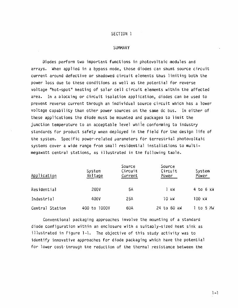
Conventional packaging approaches involve the mounting of a standard diode configuration within an enclosure with a suitably-sized heat sink as illustrated in Figure 1-1. The objective of this study activity was to identify innovative approaches for diode packaging which have the potential for lower cost'through the reduction of the thermal resistance between the
5 MW
1-1
TERMINAL
HEAT SINK COVER
2 INCH WIRE Ir-----~~----INSULATING
~ho~j (NOT r-~-r----=BUS BAR TAB
TERMINAL
Figure 1-1. AMP Solarlok Diode Junction Box
diode junction and the ambient air with the associated reduction in the required heat sink surface area and through the elimination of ancillary
components required for electrical isolation and environmental protection. The module-supported packaging approac~es considered in this study are
centered around the direct use of a mounted diode cell as opposed to a conventional packaged diode. The advantages of such an implementation
include: (1) the lower thermal resistance associated with the elimination of
mounting interfaces some of which may be mechanical contact surfaces, (2) the
reduction in the volume required for the diode package, and (3) the elimination of ancillary mounting hardware such as nuts, lockwashers, insulating washers and sleeves and cathode terminals.
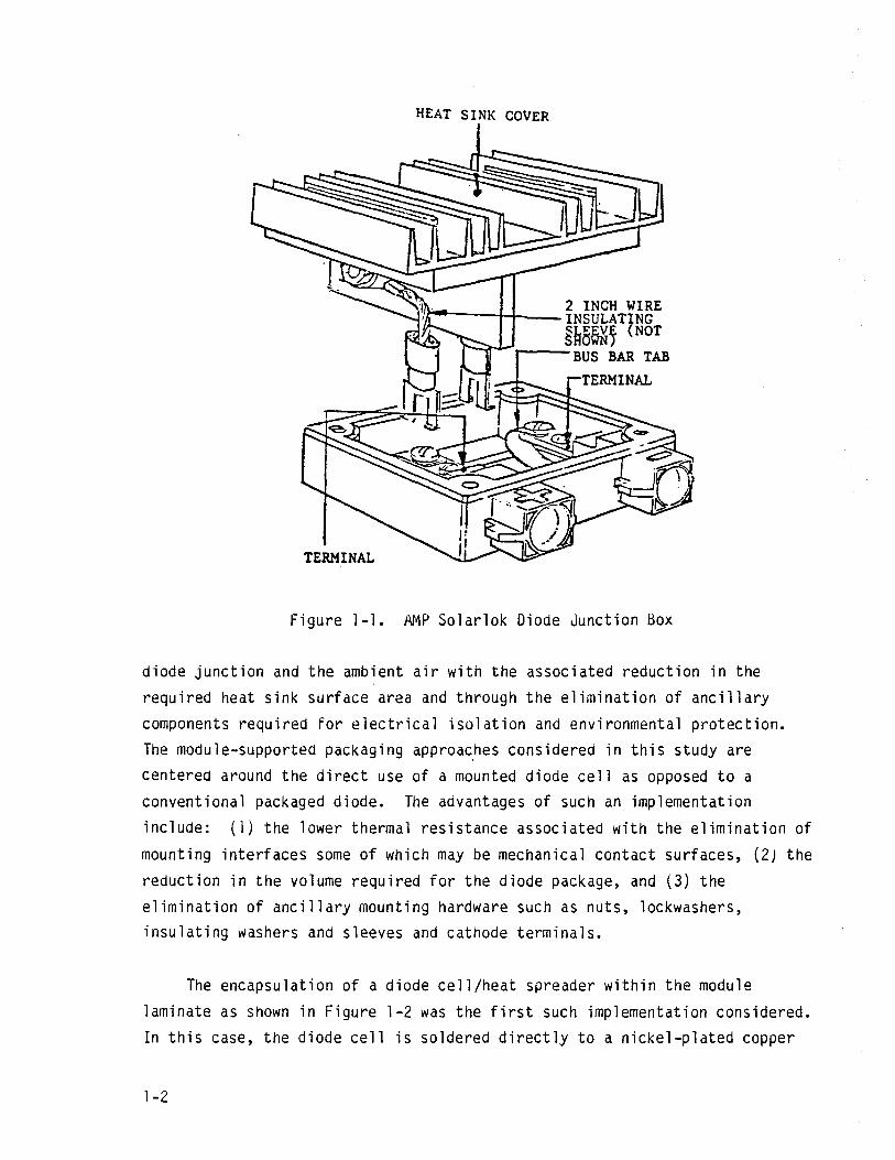
The encapsulation of a diode cell/heat spreader within the module
laminate as shown in Figure 1-2 was the first such implementation considered. In this case, the diode cell is soldered directly to a nickel-plated copper
1-2
COVERPLATE
SOLAR CELL CIRCUIT
REAR COVER SHEET
THERMAL BARRIER
Figure 1-2. Encapsulated ~pass Diode Packaging Approach
heat spreader plate and encapsulated on the rear surface of the solar cell circuit. This approach solves many of the problems inherent in an externallymounted package, including: (1) the location of a suitable mounting area which is large enough to accommodate the external enclosure with its associated heat sink, (2) the electrical bonding of the metallic heat sink to the module or array structural ground, and (3) the isolation of the electrically active parts of the diode assembly from contact by personnel. The encapsulation of bypass diodes within a module laminate is a particularly attractive solution when it is necessary, because of "hot-spot" heating considerations, to provide multiple bypass diodes within a module. Under this condition, the internally-encapsulated packaging can provide the required bypass diode protection without intermediate penetrations of the encapsulant which would otherwise be necessary to connect the externally-mounted diodes to solar cell circuit tap points.
Under other conditions, where the array designer requires a bypass diode around each series-connected module within a source circuit, it might be advantageous to consider the integration of the diode function with the module electrical terminations and wiring harness connect means. One such implementation approach, which was found to have the lowest cost of the
1-3
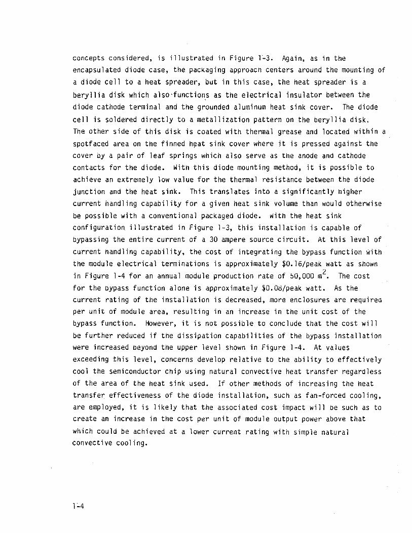
concepts considered, is illustrated in Figure 1~3. Again, as in the encapsulated diode case, the packaging approacn centers around the mounting of
a diode cell to a heat spreader, but in this case, the heat spreader is a
beryllia disk which also'functio~s as the electrical insulator between the diode cathode terminal and the grounded aluminum heat sink cover. The diode
cell is soldered directly to a metallization pattern on the beryllia disk. The other side of this disk is coated with thermal grease and located within a
spotfaced area on the finned h~at sink cover where jt is pressed against the cover by a pair of leaf springs which also serve as the anode and cathode contacts for the diode. With this diode mounting method, it is possible to
achieve an extremely low value for the thermal resistance between the diode junction and the heat sink. This translates into a significantly higher current handling capability for a given heat sink volume than would otherwise
be possible with a conventional packaged diode. with the heat sink configuration illustrated in Figure 1-3, this installation is capable of bypassing the entire current of a 30 ampere source circuit. At this level of
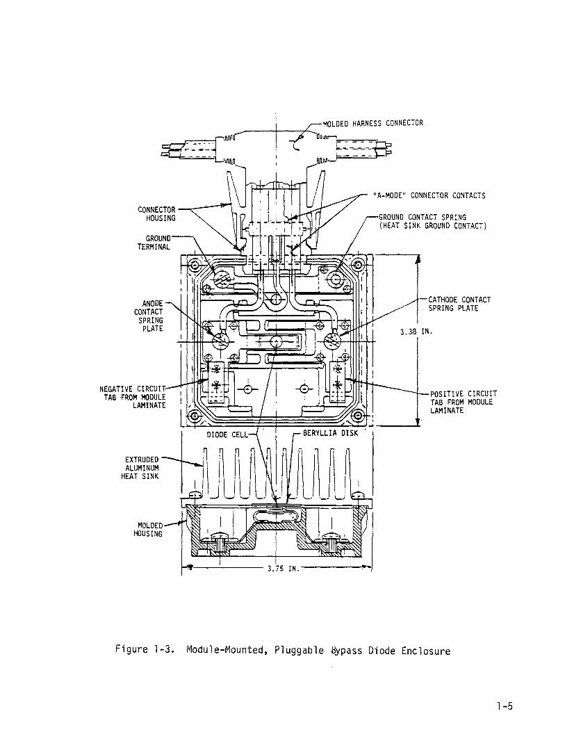
current nand1ing capability, the cost of integrating the bypass function with the module electrical terminations is approximately $0.16/peak watt as shown
in Figure 1-4 for an annual module production rate of 50,000 m2• The cost
for the bypass function alone is approximately $0.08/peak watt. As the current rating of the installation is decreased, more enclosures are required per unit of module area, resulting in an increase in the unit cost of the bypass function. However, it is not possible to conclude that the cost will
be further reduced if the dissipation capabilities of the bypass installation were increased beyond the upper level shown in Figure 1-4. At values exceeding this level, concerns develop relative to the ability to effectively cool the semiconductor Chip using natural convective heat transfer regardless of the area of the heat sink used. If other methods of increasing the heat transfer effectiveness of the diode installation, such as fan-forced cooling, are employed, it is likely that the associated cost impact will be such as to create an increase in the cost per unit of module output power above that
which could be achieved at a lower current rating with simple natural convective cooling.
1-4
ANODE CONTACT
SPRING PLATE
NEGATIVE CIRCUITTAB FROM MODULE
LAMINATE
EXTRUDED ALUMINUM
HEAT SINK
_--+----?'~__ MOLDED HARNESS CONNECTOR
=t ~ E-=-=-=-:B IUllll"-'
'------ 3.75 IN.-----~~ ... ·i
"A-MODE" CONNECTOR CONTACTS
GROUND CONTACT SPRING (HEAT SINK GROUND CONTACT)
--CATHODE CONTACT SPRING PLATE
3.38 IN.
POSITIVE CIRCUIT TAB FROM MODULE LAMINATE
Figure 1-3. Module-Mounted, Pluggable Bypass Diode Enclosure
1-5
lIc::z::
0:;:: z_ c::z::-ZM C CO ~ 0"1 1-.U ......... Z :::> Vl I.J...Z
o W_ 01-OC::Z:: ~Z 0_
::: VlO:: VlW C::Z::I-0... >- -l CO c::z::
U
~Z 0:: ~IOU -W :> -l OW 0:: 0... W
-l I.J... :::> 00
o 1-::: Vl 00 UZ
c::z::
1.0
..
"
.. -~ • 50,000 m2 MODULE AREA PER YEAR
O. 1 20 30
-RATED SOURCE CIRCUIT CURRENT (AMPERES)
Figure 1-4. Cost of Providing the Bypass Diode Function and Module Electrical Terminations
It is possible to employ the identical diode mounting and enclosure design to perform the blocking function, but for this application, it will
generally be necessary to integrate a fast-acting fuse within tne enclosure to protect the source circuit wiring in the event of a short-circuit failure of the blocking diode. Also, for the blocking application, it will be necessary to specify a diode reverse voltage rating which is consistent with the
anticipated system voltage rating.
1-6
SECTION 2
INTRODUCTION
The original objective of this contract was to research the design and processing techniques necessary to incorporate bypass diode/heat spreader assemblies within the laminate of a photovoltaic module. This objective was broadened, as a result of a subsequent contract modification, to include the conceptual design of innovative, low-cost approaches for the external mounting
of both bypass and blocking diodes. The program activity was organized into
nine major tasks as listed below:
Task - Requirements Definition
Task 2 - uesign Synthesis and Development Task 3 Component and Module Mock-up Fabrication Task 4 Bypass Diode Cost Comparison Task 5 Bypass Diode Reliability Considerations
Task 6 - Parallel Bypass Diode Load Sharing Considerations
Task 7 Thermal Cycling Endurance of Soldered Diode Cells Task 8 Bypass Diode/Enclosure Designs Task 9 Blocking Diode/Enclosure Designs
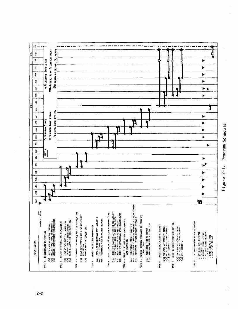
As illustrated in Figure 2-1, an annual report [lJ covering the results of the first seven task activities was issued on June 20, 1983. This final report does not duplicate the contents of this previous report but does present an overview of the general issues influencing the use of diodes in terrestrial photovoltaic systems at both the module and array design levels. This overview is followed by a detailed discussion of the various mounting approaches considered under this contract with emphasis on the module and harness-mounted enclosure designs formulated under Tasks 8 and 9.
1. "Annual Report - Photovoltaic Module ~pass Diode Encapsulation", DOE/JPL 956254-1, June 20, 1983
2-1
N I N
, l
TASK
/lHLE
STO
NE
CONT
RACT
ST
ART
TASK
1
-RE
QU
IREt
lEN
TS
DEF
INIT
ION
1(A
) D
IOD
E C
HIP
CH
ARAC
TERI
ZATI
ON
I!B
) 1
C)
MOD
ULE
FUNC
TION
AL
REQU
IREM
ENTS
M
ODUL
E CO
NSTR
UCTI
ON
REQ
UIR
EtIE
NTS
TASK
2
-O
ESIG
tl SY
NTH
ESIS
AND
DEV
ELOP
MEN
T
m!
LEAD
ATT
ACHM
ENT
CON
SID
ERA
TIO
NS
ENCA
PSUL
ATIO
N CO
NSI
DER
ATI
ON
S 2(
C)
HEAT
D
ISSI
PATI
ON
CO
NSI
DER
ATI
ON
S
TASK
3
-CO
MPO
NENT
AND
MOD
ULE
HOCK
-UP
FABR
ICA
TIO
N
3(A
) HE
AT
DIS
SIPA
TIO
N A
ND
LEAD
ATT
ACHM
ENT
EVAL
UATI
ON
3(B
) M
ODUL
E M
OCK-
UP
EVAL
UATI
ON
TASK
4
-BY
PASS
DI
ODE
COST
COM
PARI
SON
4(A
! D
ETA
ILED
PRO
DUCT
ION
COST
AN
ALY
SIS
4(B
CO
ST
COM
PARI
SON
4(C
) RE
COM
MEN
D CO
ST
REDU
CTIO
N METHOD~
TASK
5
-BY
PASS
DI
ODE
REL
lAB
ILJT
Y
CON
SID
ERA
TIO
NS
5(A
) ID
ENTI
FY
FACT
ORS
AFF
ECTI
NG
REL
IAB
ILIT
Y
5(B
) SU
RVEY
AVA
ILAB
LE
REL
IAB
ILIT
Y
DATA
5(
C)
ASS
ESS
BYPA
SS
DIOD
E R
ELIA
BIL
ITY
5(
0)
IDEN
TIFY
AD
DIT
ION
AL
DATA
REQ
UIRE
MEN
TS
TASK
6
-PA
RALL
EL
BYPA
SS
DIOD
E LD
AD .S
HA
RIN
G
CON
SID
ERA
TIO
NS
6(A
) EL
ECTR
ICA
L C
IRC
UIT
ANA
LYSI
S 6(
B)
INV
ESTI
GA
TE
VARI
OUS
MET
HODS
OF
FO
RCED
SH
ARIN
6(
C)
RECO
HMEN
D IM
PLEM
ENTA
TION
AP
PROA
CH
TASK
7
-TH
ERM
AL
CYCL
ING
ENDU
RANC
E OF
' SO
LDER
ED_
DIOD
E CE
LLS
7(A
) FA
BRIC
ATE
TE
ST
SPEC
IMEN
S 7(
8)
PERF
ORM
THE
RMAL
CYC
LING
TES
T
TASK
8 -
BYPA
SS
DIO
DE/
ENCL
OSU
RE
DESI
GNS
8(A
) ID
ENTI
FY
APP
ROPR
IATE
DI
ODES
8(
0)
DET
AIL
ED E
NClO
SURE
DE
SIGN
S a
(c)
COST
ES
TIM
ATE
TASK
9
-OL
OCKT
NG
DIO
DE/
ENCL
O':I
JRE
DESI
GNS
9(A
) tO
ENTI
FY
APPR
OPRI
ATE
DIOD
ES
9(11
) Il[
fAIL
EO E
NCLO
SIIR
E DE
SIGN
S g(
C)
COST
ES
TIM
ATE
fASK
III
-
PROG
RAM
MAN
I\GE
r~[N
T AN
D R
EPO
RTI
NG
• II
A"
liN
t CO
ST
ESTI
MAT
E •
I'Hn
f~IU
\M
I'LA
N
• M
ONTI
II Y
liT
I\HJS
I!
(PO
IHS
• 1'l
InG
RAM
R
f.VIE
U
M[[
lIN
G
• I \
/\
,11M
•
ImA
rT
I\NrW
Al
HE.P
ORT
• llH
ArT
F
INA
l H
ErO
RT
MAY ,. .. ... tJ
19
2 19
83
19
8'-
-
JUN
JU
L AU
G SE
P OC
T NO
V DE
C JA
N FE
B MA
R I A
PR
MAY 1
JUN T JUt
AIIG
1 s[ p
i OC
T NO
V D
U.
,JAN 1 f
~1I
':'[(
I 1
T
1 1
I ..- .
.. l:E
v I
t:. P
LAN
NED
ST
AR
T
• 111
LEST
ON
E C
oMPL
ET
ED
~
Q P
LAN
NED
C
oHP
LE
TI O
N
--A
CT
UA
L H
ORK
A
cC0I
1PL
ISH
HE
NT
~
()PL
AN
NE
D
OR
AcT
UA
L
SL
IPP
AG
E
-PL
AN
NE
D H
OR
K
PE
RIO
D
I I-
.. ~ --l
, ..... " .
-~ A~1r
A~ ~
A
~ ,~
<Ii Ioo
.toJ ~ ~
--.j
~,
-A
. ..,.
r7
l "1
.....
.. ~ ~
.,....,
" i
y .,.
.,. y
.,. ..
'f'
'f'
.,. .,.
.,. •
.,. .,.
.,. .,.
.,. \
.,. .6
..J
'f'
I ...
I A~._
i I
I
Fig
ure
2-1.
Pr
ogra
m S
ched
ule
SECTION 3
TECHNICAL DISCUSSION
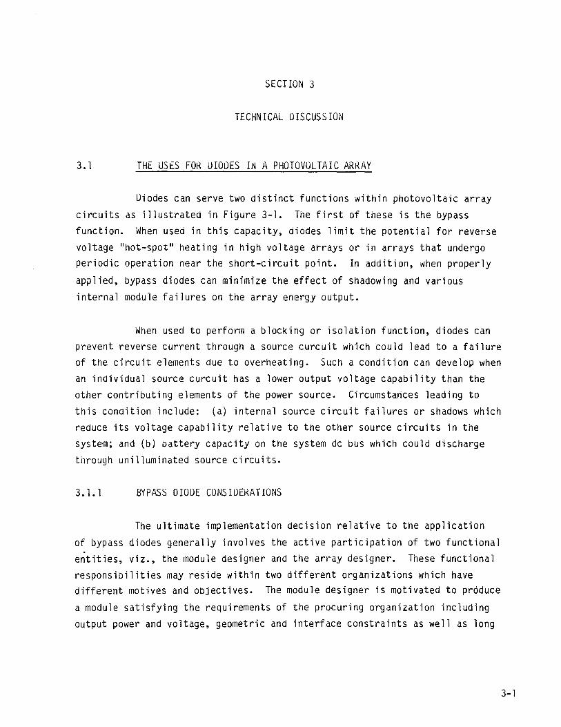
3.1 THE USES FOR UIODES IN A PHOTOVOLTAIC ARKAY
Diodes can serve two distinct functions within photovoltaic array
circuits as illustrated in Figure 3-1. The first of these is the bypass function. When used in this capacity, diodes limit the potential for reverse voltage IIhot-spot ll heating in high voltage arrays or in arrays that undergo periodic operation near the short-circuit point. In addition, when properly
applied, bypass diodes can minimize the effect of shadowing and various
internal module failures on the array energy output.
When used to perform a blocking or isolation function, diodes can prevent reverse current through a source curcuit which could lead to a failure of the circuit elements due to overheating. Such a condition can develop when an individual source curcuit has a lower output voltage capability than the other contributing elements of the power source. Circumstances leading to
this condition include: (a) internal source circuit failures or shadows which reduce its voltage capability relative to the other source circuits in the system; and (b) battery capacity on the system dc bus which could discharge
through unilluminated source circuits.
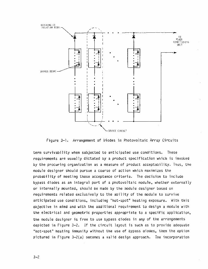
3.1.1 BYPASS DIODE CONSIDERATIONS
The ultimate implementation decision relative to the application
of bypass diodes generally involves the active participation of two functional entities, viz., the module designer and the array designer. These functional responsibilities may reside within two different organizations which have different motives and objectives. The module designer is motivated to produce
a module satisfying the requirements of the procuring organization including output power and voltage, geometric and interface constraints as well as long
3-1
BLOCKING OR
'"'''''' """E~ ~_--:,-/_/ __ '-,--
BYPASS DIODE
·1'--+--1 I
" /
. .
•
• •
•
• • •
'~- ~SOURCE CJRCUIT
TO PQ,IER
COND IT! ON I NG UNIT
Figure 3-1. Arrangement of Uiodes in Photovoltaic Array Circuits
term survivability when subjected to anticipated use conditions. These requirements are usually dictated by a product specification which is invoked
by the procuring organization as a measure of product acceptability. Thus, the module designer should pursue a course of action which maximizes the probability of meeting these acceptance criteria. The decision to include bypass diodes as an integral part of a photovoltaic module, whether externally or internally mounted, should be made by the module designer based on requirements related exclusively to the ability of the module to survive
anticipated use conditions, including Ilhot-spot" heating exposure. With this
objective in mind and with the additional requirement to design a module with the electrical and geometric properties appropriate to a specific application,
the module designer is free to use bypass diodes in any of the arrangements depicted in Figure 3-2. If the circuit layout is such as to provide adequate "hot-spot ll heating immunity without the use of bypass diodes, then the option
pictured in Figure 3-2(a) oecomes a valid design approach. The incorporation
3-2
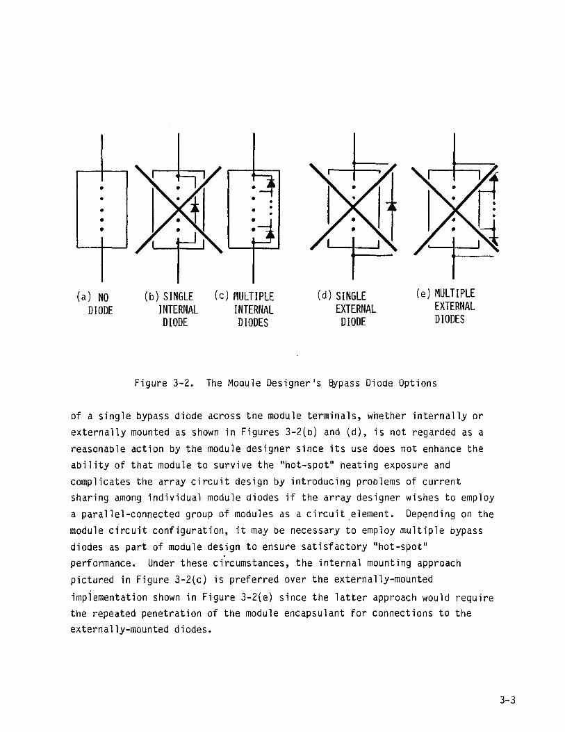
• • • • •
(a) NO DIODE
(b) SINGLE INTERNAL DIODE
(c) MULTIPLE INTERNAL DIODES
(d) SINGLE EXTERNAL
DIODE
(e) MULTIPLE EXTERNAL DIODES
Figure 3-2. The MOdule Designer1s ~pass Diode Options
of a single bypass diode across the module terminals, whether internally or externally mounted as shown in Figures 3-2(b) and (d), is not regarded as a
reasonable action by the module designer since its use does not enhance the ability of that module to survive the Ilhot-spot" heating exposure and
complicates the array circuit design by introducing problems of current sharing among individual module diodes if the array designer wishes to employ
a parallel-connected group of modules as a circuit .element. Depending on the module circuit configuration, it may be necessary to employ multiple bypass diodes as part of module design to ensure satisfactory "hot-spot" performance. Under these circumstances, the internal mounting approach pictured in Figure 3-2(c) is preferred over the externally-mounted
impiementation shown in Figure 3-2(e) since the latter approach would require the repeated penetration of the module encapsulant for connections to the externally-mounted diodes.
3-3
The motives of the array designer are somewhat broader since the measure of success in this area is the maximization of array energy output
over the operational lifetime of the installation in the face of shadowing and various internal module failures as well as the avoidance of system le~el fire
and personnel safety problems. Again, when properly installed, bypass diodes
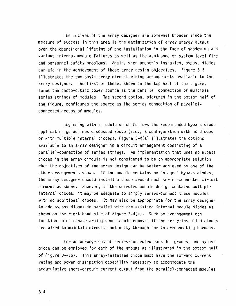
can aid in the achievement of these array design objectives. Figure 3-3 illustrates the two basic array circuit wiring arrangements available to the array designer. The first of these, shown in the top half of the figure, forms the photovoltaic power source as the parallel connection of multiple series strings of modules. The second option, pictured in the bottom half of
the figure, configures the source as the series connection of parallelconnected groups of modules.
Beginning with a module which follows the recommended bypass diode
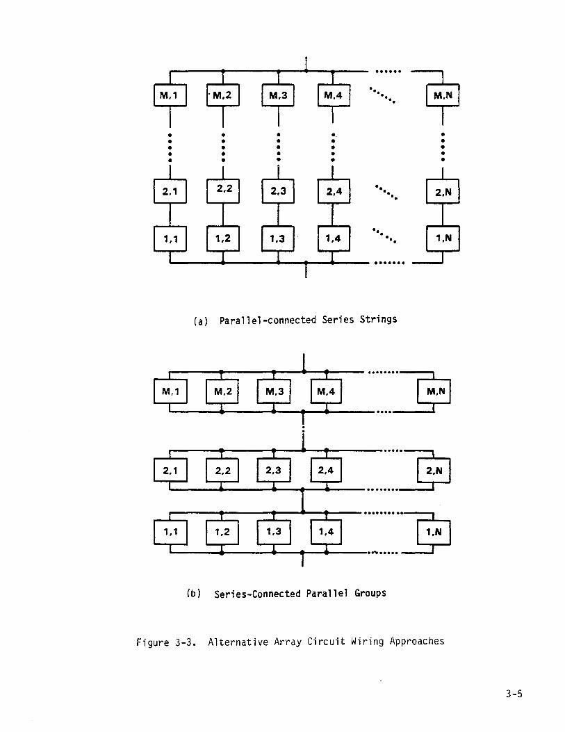
application guidelines discussed above (i.e., a configuration with no diodes or with multiple internal diodes), Figure 3-4(a) illustrates the options
available to an array designer in a circuit arrangement consisting of a
parallel-connection of series strings. An implementation that uses no bypass diodes in the array circuit is not considered to be an appropriate solution when the objectives of the array design c'an be better aChieved by one of the other arrangements shown. If the module contains no integral bypass diodes, the array designer should install a diode around each series-connected circuit
element as shown. However, if the selected module design contains multiple internal diodes, it may be adequate to simply series-connect these modules with no additional diodes. It may also be appropriate for the array designer to add bypass diodes in parallel with the existing internal module diodes as
shown on the right hand side of Figure 3-4(a). Such an arrangement can function to eliminate arcing upon module removal if the array-installed diodes
are wired to maintain circuit continuity through the interconnecting harness.
For an arrangement of series-connected parallel groups, one bypass diode can be employed for each of the groups as illustrated in the bottom half
of Figure 3-4(b). This array-installed diode must have the forward current rating and power dissipation capability necessary to accommodate the
accumulative short-circuit current output from the parallel-connected modules
3-4
••••••
~ •• •• •••
• • • .. • • • • • • • • • • • • • • • • • • • • •
•• •• ••
••• •••
•••••••
(a) Parallel-connected Series Strings
........ ~
-----+----..... --e--..----.... ~
..... 7:-1 ..... ---.... ---.... --e--4---........ ~
...•.••.. ~
-----.----..... - ..... --+--_ ......... ~
(b) Series-Connected Parallel Groups
Figure 3-3. Alternative Array Circuit Wiring Approaches
3-5
· · · • •
3-6
• • •
~
· · · ~~ • • ~
· · ~~ · • ·
(a) For Parallel-Connected Series Strings
1 I · · · ~~ • • I
1
(b) For Series-Connected Parallel Groups
• • •
Figure 3-4. The Array Designer's Bypass Diode Options
within the group. For the case where the modules are equipped with multiple
internal diodes, the installation of one large diode per group assures that the bypass current passes through the external circuit, thus avoiding the
problems associated with current-sharing among the internal diodes if no such external diodes were present.
As an outcome of this reasoning, the array designer is left with
the five acceptable diod~ electrical integration options illustrated in Figure 3-4. It is appropriate at this point to make some general observations regarding the applicability of these acceptable options to arrays of various power and voltage levels. Moderate voltage (100 to 200 vdc) and moderate
power (1 to 5 kW) arrays, which have a wide applicability to roof-mounted residential systems, can generally be characterized as having a relatively
high voltage module since the driving requirement is to develop the required
inverter input voltage level within the limited roof area available. Since the desire to maximize the module size within the constraints imposed by the roof installation will also limit the number of modules in the array, these systems will generally be configured as parallel-connected series strings where each string represents a source circuit. In such a system, the selection from among the acceptable bypass diode integration options in Figure 3-4(a) will depend on the bypass diode implementation approach adopted by the module designer. If the module voltage is sufficiently low or if the
cell reverse voltage characteristics are suffiCiently soft, the module may not
be configured with integral diodes, leaving the array designer with the requirement to install a bypass diode around each module in each source circuit. If the module voltage is high enough to require the use of multiple internal bypass diodes, it may suffice to simply series-connect these modules
to form a source circuit with no adaitional bypass diode protection. However, such an interconnection will require individual source circuit interrupts to avoid arcing when a module is removed from an illuminated array. The addition of external bypass diodes, which are connected in parallel with the internal
module diodes on the harness side of the module connect means, will eliminate this potential for arcing.
3-7
As the array voltage level and power output increase, the array interconnection scheme will be driven toward an approach using a series
connection of parallel groups as shown in Figure 3-4(b). The modules used for
such high voltage/high power applications will generally be characterized as
large in physical size with a relatively low output voltage. These two
attributes will tend to minimize the number of source circuits in the array
field, but for central station applications where the output power exceeds 1 Mw peak, it will probably still be necessary to combine modules into parallel groups within each source circuit to further limit the number of source circuits. The number of modules of a particular design in each of these parallel groups will depend on system level cost considerations which include the effects of field wiring and fault protection and isolation. For
high power array field installations, it would not be unreasonaole to expect
the individual source circuit current to exceed 60 amperes. In these cases, the single bypass diode servicing each parallel group of modules must be sized and mounted to dissipate the heat generated by this level of source circuit current. Since a single diode services a number of parallel-connected modules and since the heat dissipation capability of the diode installation dictates a
relatively massive finned heat sink, such diode installations are commonly mounted to structural components of the array frame rather than to the baCK
face of the modules. Diode installations which have dissipation capabilities in excess of 30 watts are not considered practical for mounting directly to
the surface of a module and, as such, were not considered in this study.
3.1.2 ~OCKING DIODE CONSIDERATIONS
A blocking (or isolation) diode functions to prevent reverse current through a source circuit. The usual implementation of this function involves the placement of one such diode at the top (or bottom) of each source circuit in the array. During normal sunlight operation, the full source
circuit current is required to pass through this diode. Conditions which could cause reverse current through this source circuit include:
3-8

1. A short-to-ground fault near the top of the source circuit,
2. The forward conduction of one or more bypass diodes within the source circuit,
3. The short-circuit failure of one or more modules within the
source circuit,
4. The external availability of a voltage source on the system dc bus during nighttime periods.
The presence of any of these conditions will cause the blocking diode to be
reverse biased and function to prevent reverse current through the source
circuit.
This blocking diode function imposes specific operating conditions which differ from those which characterize the bypass diode in the following areas:
a. The blocking diode functions normally in the forward current conducting mode at the full level of available source circuit current, whereas the bypass diode is normally required to operate in the reverse voltage blocking mode. This difference in fundamental operating modes has a major impact on the diode
reliability. In the blocking diode case, the device is
required to spend the majority of its operational life at the relatively high junction temperature resulting from the flow of
available source circuit current. On the other hand, the bypass diode is normally subjectea to a low level of reverse
voltage while operating at a relatively low junction temperature.
3-9
b. ~hen called upon to perform its protective function, the blocking diode is required to prevent current at a reverse
voltage which is potentially equal to the system dc bus voltage
level, whereas the bypass diode is required to conduct a
forward current which could approach the short-circuit current
capability of the source circuit.
Notwithstanding the fundamental difference in device reliability which results from the diametric operating conditions, the same diode packaging design will accommodate either function with only one important
difference, i.e., the blocking diode and its packaging design must be capable of withstanding the stresses imposed by reverse voltage operation at the system dc bus level. The diode used in a olocking application must have a rated reverse voltage which is consistent with the system voltage level. This requirement is significantly different from that associated with a bypass diode application where the reverse voltage is usually limited to about 15 vdc.
3.2 DESIGN REQUIREMENTS INFLUENCING THE APPLICATION OF DIODES
The application of diodes to terrestrial photovoltaic modules and arrays is directly influenced by the design requirements associated with the
end product as typified by the proposed UL Standard [2J. In addition to the environmental stresses imposed by the well-known Block V level testing, this UL document defines other generic requirements which are thought to relate
directly to the use of diodes in these applications. The following discussion is meant to highlight these areas. The reader should refer to the UL document if further detailed information is required on any item.
1. Polymeric materials serving as the enclosure for live parts shall:
2. UL 1703, "Proposed First Edition of the Standard for Flat-Plate Photovoltaic Modules and Panels", March 1984
3-10
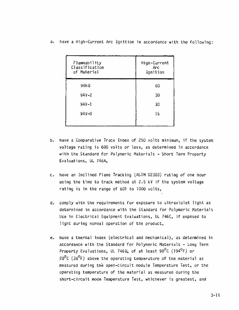
a. have a High-Current Arc Ignition in accordance with the following:
Flammability High-Current Classification Arc of Material Ignition
94H8 60
94V-2 30
94V-l 30
94V-0 15
b. have a Comparative TracK Inaex of 250 volts minimum, if the system voltage rating is 600 volts or less, as determined in accordance with the Standard for Polymeric Materials - Short Term Property Evaluations, UL 746A,
c. have an Inclined Plane Tracking (ASTM 02303) rating of one hour
using the time to track method at 2.5 kV if the system voltage rating is in the range of 601 to 1000 volts,
d. comply with the requirements for exposure to ultraviolet light as determined in accordance with the Standard for Polymeric Materials Use in Electrical Equipment Evaluations, UL 746C, if exposed to light during normal operation of the product,
e. have a thermal index (electrical and mechanical), as determined in accordance with the Standard for Polymeric Materials - Long Term Property Evaluations, UL 7468, of at least 900 C (194oF) or
200 C (36oF) above the operating temperature of the material as measured during the open-circuit module Temperature Test, or the operating temperature of the material as measured during the
short-circuit mode Temperature Test, whichever is greatest, and
3-11
3-12
f. have a minimum flame spread index of 100 as determined under the Standard Method of Test for Surface Flammability of Materials
Using a Radiant Heat Energy Source, ASTM E162-l981A.
2. Strain relief shall be provided so that stress on a lead intended for field connection, or otherwise likely to be handled in the field,
including a flexible cord, is not transmitted to the connection inside the module or panel. The test of this feature shall consist of a 20
pound (89 newton) force applied for one minute in any direction permitted by the construction, without damage to either the lead, the
connecting means or the module or panel.
3. The free length of a lead for field connection shall be at least 6 inches (152 mm).
4. A module or panel shall have a provision for grounding all accessible conductive parts which are not part of the electrical circuit. The grounding means shall be bonded to each such conductive part that is
accessible during normal use. Bonding shall be by a positive means, such as clamping, riveting, bolted or screwed connectors, welding, soldering (all joints in the bonding path shall be mechanically secure independent of any soldering) or brazing. Accessibility shall be
judged using the probe illustrated in Figure 15.1 of UL 1703. A cover that may be removed without the use of a tool is to be removed for the purposes of this requirement.
5. No accessible part of a module _or panel shall involve a risk of electric shock. In this context, the risk of electric shock is
considered to be present at a part if the potential oetween the part and earth ground or any other accessiole part is more than 30 vdc and
the leakage current exceeds the allowable values specified in the following table.
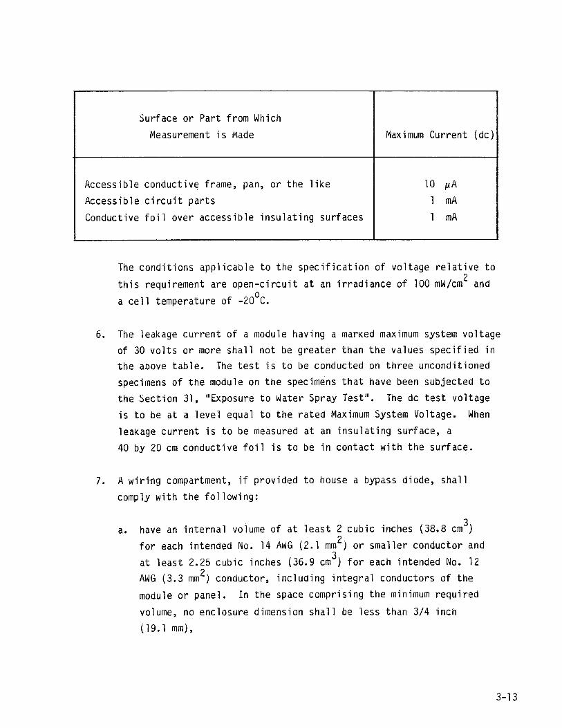
Surface or Part from Which
Measurement is Made Maximum Current (dc)
Accessible conductive frame, pan, or the like 10 I1A
Accessible circuit parts 1 rnA
Conductive foil over accessible insulating surfaces 1 rnA
The conditions applicable to the specification of voltage relative to
this requirement are open-circuit at an irradiance of 100 mW/cm2 and o
a cell temperature of -20 C.
6. The leakage current of a module having a marked maximum system voltage of 30 volts or more shall not be greater than the values specified in the above table. The test is to be conducted on three unconditioned specimens of the module on the specimens that have been subjected to the Section 31, "Exposure to water Spray Test". The dc test voltage is to be at a level equal to the rated Maximum System Voltage. When
leakage current is to be measured at an insulating surface, a 40 by 20 cm conductive foil is to be in contact with the surface.
7. A wiring compartment, if provided to house a bypass diode, shall
comply with the following:
a. have an internal volume of at least 2 cubic inches (38.8 cm3)
for each intended No. 14 AwG (2.1 mm 2) or smaller conductor and
at least 2.25 cubic inches (36.9 cm3) for each intended No. 12 AWG (3.3 mm 2) conductor, including integral conductors of the
module or panel. In the space comprising the minimum required
volume, no enclosure dimension shall be less than 3/4 inch ( 19. 1 mm),
3-13
3-14
b. have provision for connection to a wiring system employing a raceway or cable,
c. have no more than one opening when the modul~ or panel is shipped
from the factory. Tapped holes with screwed-in plugs are not
considered openings.
d. gaskets and seals shall not deteriorate beyond limits during accelerated aging, and shall not be used where they may be subject to flexing during normal operation.
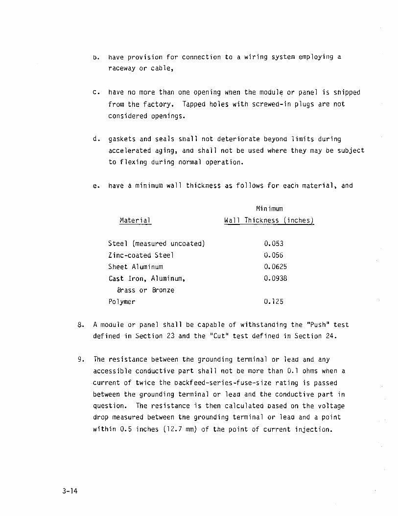
e. have a minimum wall thickness as follows for each material, and
Material
Steel (measured uncoated)
Zinc-coated Steel Sheet Aluminum Cast Iron, Aluminum,
Brass or Bronze Polymer
Minimum Wall Thickness (inches)
0.053
0.056 0.0625
0.0938
o. 125
8. A module or panel shall be capable of withstanding the "Push" test defined in Section 23 and the "Cut" test defined in Section 24.
9. The resistance between the grounding terminal or lead and any accessible conductive part shall not be more than 0.1 ohms when a
current of twice the backfeed-series-fuse-size rating is passed between the grounding terminal or lead and the conductive part in question. The resistance is then calculated based on the voltage drop measured between the grounding terminal or lead and a point
within 0.5 inches (12.7 mm) of the point of current injection.
10. The insulation and spacings between live parts and accessible conductive parts and between live parts and exposed non-conductive
surfaces sha-11 withstand the app1 ication of a test voltage equal to 2x system voltage plus 1000 volts without the leakage current between these two points exceeding 50 ~A. The test is to be conducted on
three unconditioned specimens as well as the specimens that have been subjected to IIExposure to Water Sprayll, Section 31; IITemperature Cyc1ingll, Section 33; II Humidityll, Section 34; and IICorrosive
Atmosphere", Section 35. For the testing of components with exposed
insulating parts, the parts are to be coverea with conductive foil.
11. There shall be no accessibility to live parts when the module is
subjected to the impact from a 2 inch (51 mm) diameter smooth steel
sphere weighing 1.18 pounds (535 grams) falling through a distance of
51 inches (1.295 m).
12. When tested per the requirements of Section 31, IIExposure to Water Sprayll, the design shall prevent the collection of water in a compartment containing live parts. Immediately following this test exposure (with no drying of the samples), the module or panel shall comply with the dielectric voltage withstand test of Section 26, and the leakage current test of Section 21.
13. Materials used for gaskets and seals shall conform to the specific requirements of Section 32 and shall not deform, melt, or harden to a degree which would affect its sealing properties.
3-15
3.3 BYPASS DIODE IMPLEMENTATION OPTIONS
3.3. 1 INTERNALLY ENCAPSULATED
The lamination of bypass diodes within the module encapsulant as shown in
Figures 3-5 ana 3-6 solves many of the problems associated with the mounting
of conventional packaged diodes external to the module, including: (1) the
location of a suitable mounting area which is large enough to accommodate the
rather bulky diode package and associated heat sink, (2) the electrical isolation of the diode case, which is usually the cathode connection of the
diode, from the metallic heat sink, (3) the electrical bonding of the metallic
heat sink to the module or array structural ground, and (4) the isolation of
the electrically active parts of the bypass diode assembly from contact by
personnel.
The soldered assembly of the diode cell to the heat spreader plate can be conveniently laminated on the rear side of the solar cell circuit where direct
connections to the circuit terminations are possible. This relatively thin package can be readily accommodated within the existing encapsulant system
where it is electrically isolated from the surroundings and environmentally protected. The construction details of this design approach along with a
supporting production cost analysis are presented in Reference 1. The heat
spreader plate size required to accommoaate the diode heat dissipation associated with a particular short-circuit current rating is given in
Figure 3-7 based on experimental data obtained on representative module
segments as reported in Reference 1. This data base has been expanded over
that contained in the reference to account for a variation in both the
allowable EVA exposure temperature limit and in the ambient temperature.
Consistent with the constraint imposed by the experimental set-up, the rear
surface of the module is assumed to be adiabatic. This will lead to a
conservative over prediction of tne heat spreader area required for a
specified level of diode heat dissipation for the general case where some
heat rejection occurs at the module rear surface.
3-16
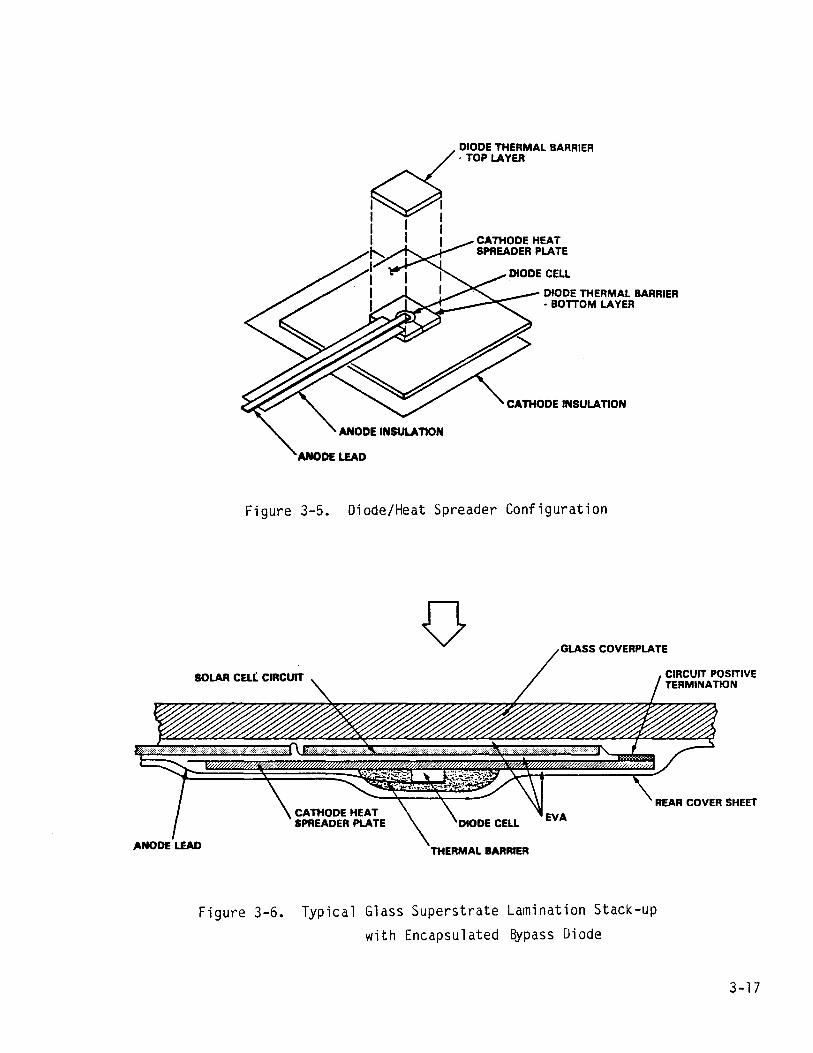
d DIODE THERMAL BARRIER • TOP LAYER
I I I I I I I I I I "I I I DIODE THERMAL BARRIER I . BOTTOM LAYER
CATHODE INSULATION
Figure 3-5. Diode/Heat Spreader Configuration
ANODE LEAD
Figure 3-6.
GLASS COVERPLA TE
REAR COVER SHEET CATHODE HEAT SPREADER PLATE
THERMAL BARRIER
EVA
Typical Glass Superstrate Lamination Stack-up
with Encapsul ated Bypass Di ode
3-17
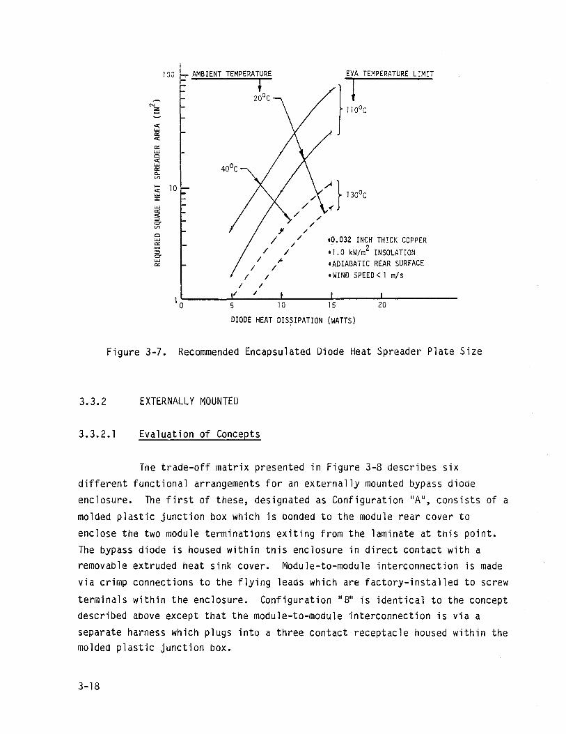
N Z -ex: L.U 0:: ex: 0:: L.U 0 ex: L.U 0:: c.. (./)
!o-ex: UJ :I:
UJ 0:: ex: =:l 0-(./)
0 UJ 0:: -=:l 0-UJ 0::
I 100 t: AMBIENT TEMPERATURE
I t
10 -
/ I
5
20°C
/ / /
/ ~ I /
10
.0.032 INCH THICK COPPER
.1.0 kW/m2 INSOLATION
.ADIABATIC REAR SURFACE 'WIND SPEED< 1 m/s
DIODE HEAT DISSIPATION (WATTS)
Figure 3-7. Recommended Encapsulated Diode Heat Spreader Plate Size
3.3.2 EXTERNALLY MOUNTEU
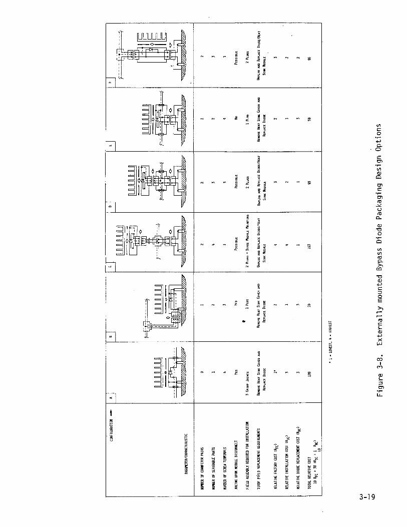
3.3.2.1 Evaluation of Concepts
The trade-off matrix presented in Figure 3-8 describes six different functional arrangements for an externally mounted bypass diode enclosure. The first of these, designated as Configuration "A", consists of a
molded plastic junction box which is bonded to the module rear cover to
enclose the two module terminations exiting from the laminate at this point. The bypass diode is housed within tnis enclosure in direct contact with a removable extruded heat sink cover. Module-to-module interconnection is made via crimp connections to the flying leads which are factory-installed to screw
terminals within the enclosure. Configuration "8" is identical to the concept described above except that the module-to-module interconnection is via a separate harness which plugs into a three contact receptacle housed within the molded plastic junction box.
3-18
W I \D
CONF
IGUR
ATIO
N -
PARA
I'lTER
lCHA
RACT
ERIS
T IC
NIlltB
ER O
F CO
HItE
CTOR
PAI
RS
NUMB
ER O
F SE
PARA
BLE
PART
S
NIilIB
ER O
F SC
REW
TERI
1INAL
S
ARCI
NG U
PON
I«JDU
LE D
ISCO
NNEC
T
FIEL
D AS
SEllB
LY R
EQUI
RED
FOR
INST
ALLA
TION
DIOD
E FI
'ELD
REP
LACE
MENT
REQ
UIRE
HENT
S
RELA
TIVE
FACT~Y C
OST
(RFC
)
RELA
TIVE
IN
STAL
LATI
ON C
OST
(RIC
)
RELA
TIVE
DIO
DE R
EPLA
CEME
NT C
OST
(RRC
)
TOTA
L RE
LATI
VE C
OST
10 R
FC +
30
(RIC
+ ~ R
RC)
~
~
~
~
~
ruw
uw]
~-<:>--~
fIJlJlJ
lJUJl
~
. -0
-
-;l=!------~
+ ~
[UlJW
W]
? 0
Ul-l
LtU
I
WW
W
~ ~--h-7
I I =
= ...
=~
~
-~
~ ~ ~
vzw.
0 ]
2 2
]
] 2
4 3
2
4 3
3 3
4
Y'S
Y'S
POSS
IBL
E
POSS
IBL
E
No
• 3
CR
IMP
jo
iNT
S
1 PL
UG
2
PLU
GS
+ D
IOD
E M
oDUL
E rt
JUN
TIN
G
2 PL
UGS
] PL
UG
REM
OVE
H
EAT
SIN
K
COVE
R AN
D RE
HO
VE
HEAT
SI
NK
CO
VER
AND
UN
PLU
G
AND
REP
LAC
E D
IOD
E/H
EA
T
UN
PLU
G
AND
REP
LAC
E D
IOD
E/H
EA
T
REM
OVE
H
EAT
SIN
K C
oVER
AN
D
REP
LAC
E D
IOD
E RE
PLAC
E DI
ODE
SI
NK
M
oDUL
E SI
NK
M
oDU
LE
REP
LAC
E D
IOD
E
].
2 4
3 2
3 ]
4 2
]
3 3
] ]
3
]09
59
]63
93
59
I •
] •
LOW
EST,
4 •
HIGH
EST
Fig
ure
3-8.
E
xter
nall
y m
ount
ed
Byp
ass
Dio
de
Pac
kagi
ng
Des
ign
Opt
ions
~
-
r----a
r---=
']
~t~ ~
'.
2 3 3
POSS
IBL
E
2 PL
UG
S
UNPL
UG
AND
REP
LAC
E D
IOD
E/H
EA
T
SIN
K
P',oD
ULE 3 2
, 2 96
J
In confi~uration "C", the junction ,bo.x containing the diode and heat sink is divorced from the module so that it can be separately mounted to
other support structure. The harness is then required to connect between
modules as well as to connect from the module to the diode junction box.
Configuration "0" is a variation to Configuration "C" which
supports the separate diode junction box from the module rear surface through an intermediate connection fitting that forms part of the module-to-module wiring harness.
This latter arrangement can be further simplified by incorporating
the diode junction box as part of the module-to-module wiring harness to form
the configuration designated as "E" in the figure.
The final integration scheme, shown schematically as Configuration "F",
attaches the diode enclosure directly to the module-mounted receptacle as in Configuration "E", but uses a pluggable connector interface with the
module-to-module wiring harness.
Figure 3-8 summarizes the results of a comparative cost assessment among these various implementation options. This assessment was performed by
first quantifying the physical characteristics thought to have a significant bearing on the initial factory cost of the diode enclosure and ancillary
components. These include: (a) the number of connector pairs, (0) the number of separate manufactured subassemblies, and (c) the number of screw terminals within the diode enclosure. The factory cost for each configuration was considered to be directly related to the sum of the values assigned to each of these parameters. The resulting numerical total was normalized on a scale of 1 to 4, with 1 being the lowest cost, to yield the relative factory cost
(R FC ) given in the figure. This formulation results in Configuration "A" having the lowest factory cost, followed by Configurations "811 and "E" and concluding with Configuration "C" at the high end of the scale. This result
seems to be intuitively correct based on the pictorial schematic given for each approach.
3-20
The field assembly required for the installation of each configuration is described and used to determine the relative installation
cost, ranging from "1" (or lowest) for one plug connection to "411 (or highest)
for two plug connections plus the mounting of a separate diode enclosure.
The relative cost for the field replacement of defective bypass
diodes is assessed based on the features of the packaging design. When it is
possible to restore the bypass diode function by the removal and replacement
of the diode enclosure by the simple separation of a connector joint, the
concept is judged to have the lowest field replacement cost. When the
enclosure is permanently mounted to the module, it is necessary to open
the enclosure to remove and replace the diode in the field, resulting
in the highest relative cost for diode replacement. In the case of
Configuration "E", a defective diode function could be restored by the
removal and replacement of the complete harness assembly for a source
circuit. This was also judged to have the highest relative cost for diode replacement.
This assessment was completed by combining these three relative cost parameters to derive a total relative cost figure-of-merit. The
algorithm for this total relative cost, as presented on the last row of the figure, accounts for the fact that the field labor rate is approximately three
times that for factory labor and for the reduced frequency of diode
replacement relative to the initial installation. In accordance with the
algorithm used for this computation, the high cost of field labor strongly
penalizes those concepts requiring a relatively high installation cost,
whereas the lower frequency of bypass diode replacement de-emphasizes the
importance of this cost factor. By this methodology, Configurations "8"
and "E" were judged to have the potential for the lowest total life cycle cost and were therefore selected as the implementation options to be developed
further through a design phase Wh1Ch would include drawing definition and a subsequent detailed costing analysis and comparison.
3-21
3.3.2.2 Design of Promising Packaging Approaches
3.3.2.2.1 Diode Mounting
The previous work which led to the definition of an integral
diode/heat spreader for direct lamination within the module encapsulant forms the logical basis for the formulation of an integral diode cell mounting approach having a broad applicability to innovative, low-cost, externally
mounted bypass diode enclosures. In particular, the direct utilization of a mounted diode chip or cell in lieu of a conventional packaged diode can yield
the following advantages.
• Reduced thermal resistance between the diode junction and the mounting interface. The elimination of the diode package body with its ancillary electrical isolation hardware will reduce the
number of mounting interfaces with an associated decrease in tnermal resistance.
• Enhanced dielectric isolation by virtue of the direct solder attachment of the diode cell to a ceramic insulating substrate.
• Reduced package volume and cost associated with the elimination of the bulky diode body and associated mounting hardware.
The potential for reduced thermal resistance in the heat flow path is of particular significance since this parameter, which is identified as Rejs in Figure 3-9, has a direct .influence on the heat sink required to
limit the diode junction temperature during worst-case ambient temperature conditions. Using the nomenclature defined in Figure 3-9, the heat dissipation capaoility of the mounted diode, Q, is given by:
Q = T. - T J a
3-22
~ Q : Diode Heat Dissipation
Diode Junction Temperature (T.) .J
Heat Sink Temperature (T ) s
~ Ambient Air Temperature (T ) a
Figure 3-9. Thermal Path Between the Diode Junction and Ambient
A concept which mounts the diode chip to a beryllia (BeO)
substrate, as shown in Figure 3-10, can minimize the junction-to-heat sink thermal resistance and thus permit the use of a more compact heat sink component for the same junction temperature rise above ambient under a given diode heat dissipation condition. At the same time, the beryllia wafer provides the high withstanding voltage required for application in higher voltage systems. Beryllia, witn its high dielectric strength, high thermal
conductivity and low linear thermal expansion, is ideally suited to this
application. !n the mounting configuration pictured in Figure 3-10, the silicon die is soldered directly to a nickel-plated copper metallization pattern which is bonded directly to the beryllia wafer using a process developed and licensed by the General Electric Company. As shown in
figure 3-11, this process depends upon the existence of a eutectic in the
copper-oxygen system to produce a strongly adherent bond between the metal and the ceramic surface. The bond strength at this interface can exceed 138 MPa
(20,000 psi), a value which is many times that achievable with thick film pastes. In addition, a thick film layer will have a higher thermal resistance
than a direct bonded copper foil, resulting in a higher junction temperature
3-23
, SILICON DIE WITH ALUMINUM '",ANODE PAD
......... "-.. , " /
BERYLLIA \o1,Il,FER SUBSTRATE
,
DIRECT-BONDED COPPER CATHODE METALLIZATION
Figure 3-10. PN Junction uiode Cell Mounted to bery11ia Substrate
Ll/
II '. 1150 2100
1125
/ ~1+~ /' \ ' i'J
1100
1075
,....~
1050
Ll + cu20
2000
~+cu20
ZZlOld Cu FOIL
CERAMIC SUBSTRA TE lal
0.3 0.6 0.9 1.2 .1.5 1.S
3-24
WEIGHT PERCENTAGE OXYGEN Cu~
;zzzzzzzzzi
~-. INITlAL CONDITlON HEAT-UP IN AT ROOM TEMPERATURE OXIDIZING ATMOSPHERE
EUTECTIC
BONDING AT 1065" < T < 10S:T
Figure 3-11. Direct-Bonded Copper
CU+CU20 , ¥,t:;::Z;::Z::;:Z::;=;Z:;Z;::Z;::Z;=Z;:(
-.~ FINAL BOND AFTER COOL·DOWN

for a given dissipation. Another important advantage of the direct-bonded copper metallization when compared to thick film metallization is its
significantly lower sheet resistance, i.e., the resistance of a 250~m (0.010 inch) thick dir~ct-bonded copper foil be approximately 0.1 mn per square compared to values in the range of 1.5 to 4.4 mn per square for typical thick film metallizations.
The thermal expansion/contraction characteristics of this mounting susbstrate will be controlled by the beryllia wafer since its thickness is at least five times that of the copper metallization layer. Thus, this mounting approach, which eliminates one of the aluminum pads normally present on both
sides of the die, provides for the close matching of the thermal expansion
characteristics of the die and the heat conducting beryllia substrate. This thermal expansion compatibility should combine with the fatigue resistance of the high lead solder to produce a joint with stable thermal conductivity when subjected to the temperature cycling environment.
The heat transfer through this stacked assembly of diode cell and beryllia disk is modelled as a combination of discrete thermal resistance terms as illustrated in Figure 3-12 [3J. The R 81 term accounts for the thermal resistance of the cylindrical stack-up of the silicon die with its interfacial layers of metallization and solder. Tne value of R 81 is evaluated by:
n 4
= "d2L ;=1
t. 1
r 1
where t; and ki are the thickness and thermal conductivity, respectively, of each separate material layer in the stack-up. For the packaging
[3J A.J. Yerman, "Tne Analysis and Measurement of Thermal Resistance in Power Semiconductors II GE Report No. 83CR0134, June 1983.
3-25
I""""" o
d-~"-I t. J
-------t s
Interfacial Heat Transfer Coefficient, h
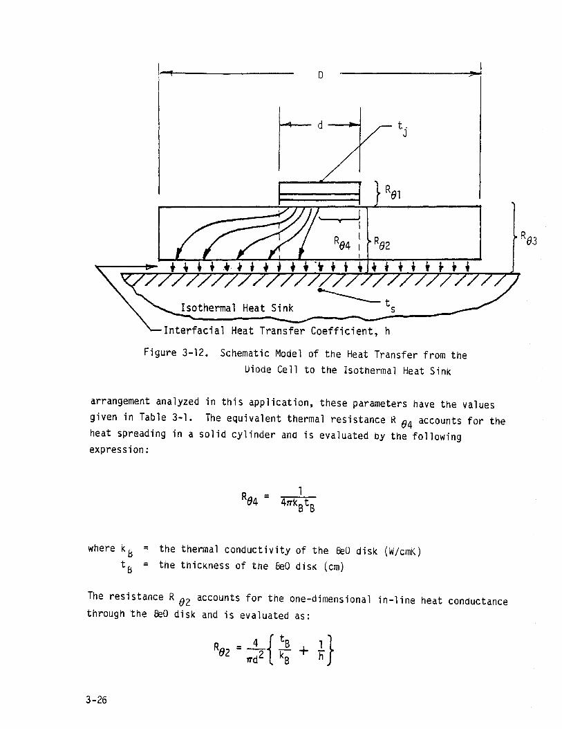
Figure 3-12. Schematic Model of the Heat Transfer from the Uiode Cell to the Isothermal Heat Sink
,...1
arrangement analyzed in this application, these parameters have the values given in Table 3-1. The equivalent thermal resistance R 04 accounts for the heat spreading in a solid cylinder and is evaluated by the following expression:
1
where KB = the thermal conductivity of the feO disk (W/cmK) t8 = tne thicKness of the BeO disk (cm)
The resistance R 02 accounts for the one-dimensional in-line heat conductance through the feO disk and is evaluated as:
3-26
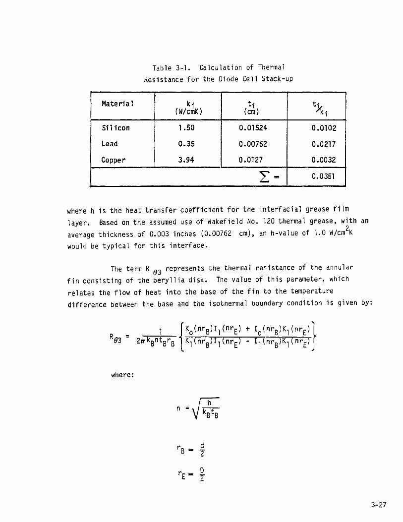
Materia 1
Silicon
Lead
Copper
Table 3-1. Calculation of Thermal Resistance for the Diode Cell Stack-up
k; (W/cmK )
t; (cm)
1.50 0.01524
0.35 0.00762
3.94 0.0127
z:=
t,k k . , 0.0102
0.0217
0.0032
0.0351
where h is the heat transfer coefficient for the interfacial grease film layer. Based on the assumed use of Wakefield No. 120 thermal grease, with an average thickness of 0.003 inches (0.00762 em), an h-value of 1.0 W/cm
2K
would be typical for this interface.
The term R 83 represents the thermal rec:istance of the annular fin consisting of the beryllia disk. The value of this parameter, which
relates the flow of heat into the base of the fin to the temperature difference between the base and the isothermal boundary condition is given by:
where:
n = V k;ts
rs = d 2"
rE = 0 2"
3-27
10 and 11 are modified Bessel functions of the first kind evaluated for the arguments (nr S) or ( nrE)
KO and Kl are modified Bessel function of the second kind.
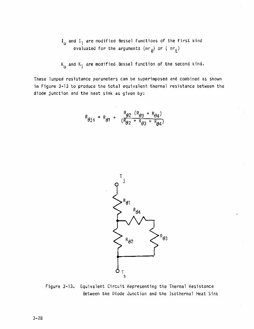
These lumped resistance parameters can be superimposed and combined as shown in Figure 3-13 to produce the total equivalent thermal resistance between the diode junction and the heat sink as given by:
3-28
Figure 3-13. Equivalent Circuit Representing the Thermal Resistance Between the Diode Junction and the Isothermal Heat Sink
The results of this analysis are shown in Figure 3-14 where the thermal resistance between the diode junction and a point immediately on the
isothermal heat sink side of the grease joint interface between this heat sink
and a beryllia (BeO),disk is plotted as a function of physical parameters including die diameter (d), BeO disk diameter (D) and thickness (t a). These data reveal the importance of tne BeO disk in spreading the heat flow path so that the area of the grease interface is effectively increased, resulting in its reduced impact on the overall thickness resistance of the stack-up. For the larger disk diameters (d/D < 0.6), the thickness of the disk has a
significant effect on the overall thermal resistance of the assembly as
illustrated in Figure 3-15, where the overall R 8js value. has been plotted
as a function of disk thickness (t S) for disk diameters of 0.50 and 1.00
inches and for silicon die diameters of 0.14 and 0.22 inches. In all cases,
there is a significant improvement in the overall conductance of the assembly
as the BeO disk thickness is increased from 0.025 inches to 0.093 inches, but a substantially diminished improvement as the thickness if further increased to 0.150 inches, particularly if the disk diameter is restricted to a maximum of 0.50 inches by BeO wafer cost considerations.
The selection of silicon die size and BeO wafer diameter and
thickness cannot be made independent of a consideration of heat sink size
since the former parameters determine the R Ojs value while the heat sink size is directly related to the Rosa value. As shown in Figure 3-9, it is the sum of these two thermal resistance values that determines the ability of the assembly to achieve a given junction temperature rise under a specified heat dissipation condition. As the silicon die and BeO disk are reduced in
size to minimize the cost of these components, the corresponding R Ojs value will increase forcing a commensurate decrease in the required R Q value.
v sa This decrease in R 8sa requires a correspondingly larger heat sink with associated higher cost. Conversely, the specification of an undersized heat sink will force a correspondingly lower value of R Ojs which can only be
acnieved by specifying a larger silicon die and/or BeU wafer size.
3-29
10 I. .. d (0.003 in thick)
Sllicon Die I d 0.14" (0.012 in thick) /'
COIlper I I 9
[0.00' ,. "'I' ts I
I
8 l 7 i
I
6 I -... ... ~ 5 3 ..... u
!: 0
d = 0.22" 11'1 . ...,
q) a::
I / 4
// 3 )'
I
2
ta (inches)
0.025 ... ¥' -------- 0.093 .....
----- 0.150
0
0 0.2 0.4 0.6 0.3 1.0
diD
Figure 3-14'. Thermal Kesistance of the Uiode Ce11/8ery11ia Disk Assemoly
3-30
2.0
I-
!:;C ::£ 1.0 ...... u o
--.,. -+
o = 1.00 inches
o = 0.50 inches
d
(inches)
0.14
0.22
o~ __ ~ __ ~ __ ~ __ ~ __ ~ __ ~ __ ~ __ ~ __ ~ __ ~ ______ _
o 0.1 0.2 tR (inches)
Figure 3-15. The Effects of Sea Wafer Thickness on the Overall Stack Thermal Resistance
Thus, it is apparent that a cost optimum exists for the assembly
consisting of the silicon die, HeO disk and finned aluminum heat sink. Figure 3-16 gives the results of a cost optimization analysis performed for
20 watts of diode heat dissipation. Silicon die diameters of 0.14 and 0.22 inches were considered, with associated unit costs of $0.17 ana $0.42,
respectively, for a quantity of 50,000 parts. BeO disk costs are presentea in Figure 3-17 as a function of diameter and thickness based on data supplied by
a beryllia supplier for a quantity of 50,000 parts. The pricing discontinuity which occurs between a disk diameter of 0.5 and 0.75 inches is associated with the required use of a larger (and slower) press for diameters of 0.75 inches and larger. Subsequent discussions with this supplier have confirmed that the pricing for a U.625 inch diameter disk would follow the pattern of the smaller
diameter disks, thus yielding a unit price of $0.27 and $0.42 for 0.025 and 0.150 inch thickness material, respectively.
3-31
For a given combination of die diameter, BeO disk diameter and BeO disk thickness, the associated value of junction-to-sink thermal resistance is
obtained from Figure 3-14. The required heat sink-to-ambient air thermal
resistance for natural convective cooling can then be calculated from
Figure 3-9 if it is assumed that 750C is the maximum allowable junction
temperature rise above ambient. The resultant heat sink volume is related to this required R 8sa value by Figure 3-18. Using 0.04 lb/in3 as an average density for the finned aluminum heat sink extrusion and assuming a cost of $3.00/1b for this component, it is thus possible to develop heat sink cost as
a function of the required R 8sa value.
3-32
-C"'l IX) 0\ .... I ~ :z: -CJ')
I< Lo.I :: + ~ CJ') -Q
Q Q.I
IX)
+ Lo.I -Q
:z: o (,.) -.....I -CJ')
ICJ')
o (,.)
.....I < Io I-
7 • DIODE DISSIPATION = 20 WATTS (ROja = 3.750 C/W)
d = 0.14 inches
.. \
•
\
2-
1 - d = 0.22 inches
--.-
ts (inches)
0.025 0.150
O~ ____ ~ ____ ~ ____ ~ ____ ~ ____ -L ____ -L ____ ~ __ __
o 0.1 0.2 0.3 0.4 0.5 0.6 0.7
diD
Figure 3-16. Results of Cost' Optimization Analysis for 20 Watts of Diode Heat DiSSipation
.... "" co ~
w u :x C>.
t:; :z: :::>
I-
10.0
Thickness - (inches)
o .020 2, .025
EJ .030 ~ .062 $ .150
1.0
0.1
0.01 0.1 DISK AREA (IN)
I I I I I I 0.15 0.375 0.5 0.75 1.0 1.25 1.50
DISK DIAMETER (INCHES)
Figure 3-17. Price of BeO Insulating Disks for a Quantity of 50,000 Units
10.0 ~
8.0
• NATURAL CONVECTION 6.0
~ 4.0 ::;: ...... u
o
2.0
1.0~------L----L __ ~~~~~~ ______ ~ ____ ~ __ L-
2 4 6 8 10 20
HEAT SINK VOLUME (;n3)
Figure 3-18. The Thermal Resistance of Aluminum Heat Sinks Cooled by Natural Convection
40
3-33
The results of this analysis, as represented by Figure 3-16 display the expected cost optimum, which is somewhat distorted by the ~O disk pricing
discontinuity occurring for disk diameters of 0.75 inches and greater.
However, it is clear from these curves that, as the diameter of the disk increases and approaches 0.625 inches, there is a minimum cost optimum for a disk diameter of approximately 0.625 inches. For larger disk diameters, the
shape of this optimum is grossly distorted by the BeO disk pricing data discontinuity.
In addition to confirming that 0.625 inches is the optimum BeO disk diamet~r, this analysis shows that the selection of the 0.22 inch silicon die
diameter is warranted, even though the 0.14 inch diameter may be adequate for the rated source circuit current and may, in fact, yield a slightly lower minimum cost. The use of the 0.22 inch diameter silicon die decreases the cost sensitivity to both disk thickness and diameter, while yielding a minimum cost that is nearly identical to that achievable with the smaller die. In all
cases, the use of a relatively thick (0.093 to 0.150 inch) BeO wafer is
indicated, but this is more important if the smaller die is selected.
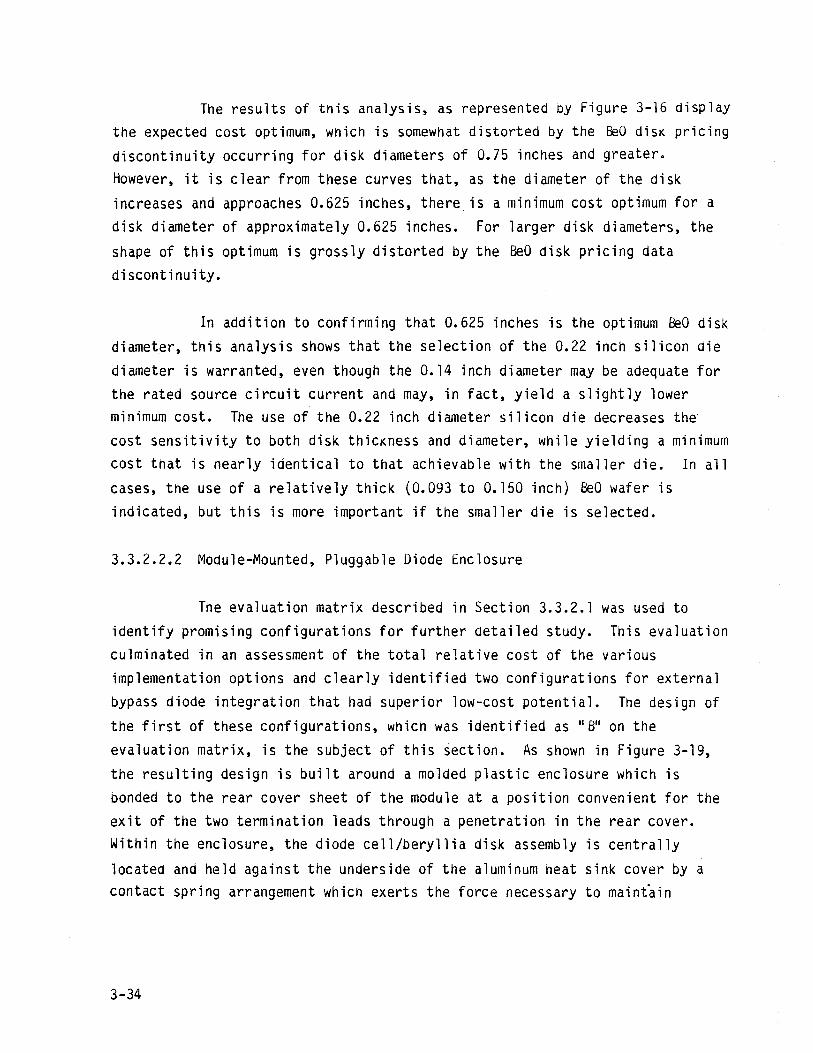
3.3.2.2.2 MOdule-Mounted, Pluggable Diode Enclosure
The evaluation matrix described in Section 3.3.2.1 was used to identify promising configurations for further detailed study. This evaluation culminated in an assessment of the total relative cost of the various implementation options and clearly identified two configurations for external bypass diode integration that had superior low-cost potential. The design of
the first of these configurations, which was identified as "~I on the evaluation matrix, is the subject of this section. As shown in Figure 3-19, the resulting design is built around a molded plastic enclosure which is bonded to the rear cover sheet of the module at a position convenient for the exit of the two termination leads through a penetration in the rear cover. Within the enclosure, the diode cell/beryllia disk assembly is centrally
located and held against the underside of the aluminum heat sink cover by a contact spring arrangement which exerts the force necessary to maintain
3-34
CONNECTOR HOUSING
ANODE CONTACT
SPRING PLATE
NEGATIVE CIRCUIT TAB FROM MODULE
LAMINATE
EXTRUDED ALUMINUM
HEAT SINK
_---I---,,:...L MOLDED HARNESS CONNECTOR _)S-[U 1lIr--1\:::-=-",=-=_
-c.. E~ -=-=-=1:f; 1Ul'~'-
~r------ 3. 75 IN.-----~
"A-MODE" CONNECTOR CONTACTS
GROUND CONTACT SPRING (HEAT SINK GROUND CONTACT)
--CATHODE CONTACT SPRING PLATE
3.38 IN.
POSITIVE CIRCUIT TAB FROM MODULE LAMINATE
Figure 3-19. Module-Mounted, Pluggable ~pass Diode Enclosure
3-35
contact at this thermal grease interface as well as providing the electrical contacts for the diode anode and cathode. These spring contacts are rigidly attached to islands, which are molded in the plastic enclosure, and are connected to the positive and negative module terminations entering through the bottom of the box. Screw terminals are provided within the enclosure to accommodate the wire connections from the receptacle mounted in the box
sidewall. Note that a ground lead is carried through this receptacle so that
the exposed heat sink cover can be grounded as required by UL 1703. This grounding is effected through a coil spring which is compressed against the underside of the cover as it is installed.
In addition to the thermal resistance reductions and enhanced dielectric isolation made possible by use of the diode cell/beryllia disk, this diode mounting concept permits the replacement of a defective diode by simply removing the heat sink cover and lifting the defective component from its contact spot on the cover.
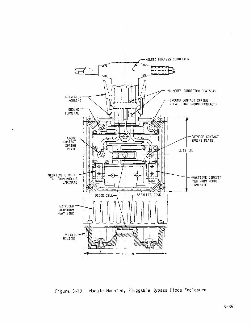
This compact enclosure design will accommodate diode heat
dissipations up to 30 watts. The heat sink configuration shown in
Figure 3-19, with an exposed surface area of 110 in 2, is capable of producing a sink-to-air thermal resistance (R esa) of approximately 2.00C/watt in a natural convection environment. when this value is combined
with the junction-to-sink thermal resistance (K ejs) associated with the selected diode/beryllia disk, as obtained from Figure 3-14, a total thermal
resistance of 2.50 C/watt is achievable with this configuration. Thus, for 30 watts of internal diode dissipation, tne enclosure design pictured in Figure 3-19 could be expected to limit the junction temperature rise to 750 C
above ambient which is an acceptable level for silicon devices. As the
dissipation requirement for the enclosure is decreased, a reduction in the size of the heat sink cover is indicated to take advantage of a reduction in the cost of this cover. At dissipation levels of 10 watts or less, a planar aluminum cover would suffice. As the dissipation increases from this value,
the finned heat sink height could be correspondingly increased until it
approaches the height illustrated in Figure 3-19 at the 30 watt level.
3-36
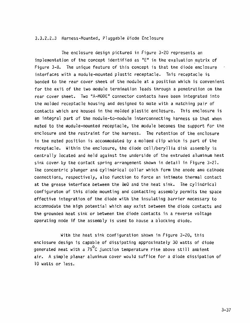
3.3.2.2.3 Harness-Mounted, Pluggable Diode Enclosure
The enclosure design pictured in Figure 3-20 represents an imple~entatjon of the concept identified as "E" in the 'evaluation ~~trix of Figure 3-8. The unique feature of this concept is that the diode enclosure interfaces with a module-mounted plastic receptacle. This receptacle is bonded to the rear cover sheet of the module at a position which is convenient for the exit of the two module termination leads through a penetration on the rear cover sheet. Two "A-MODE" connector contacts have been integrated into the molded receptacle housing and designed to mate with a matching pair of contacts which are housed in the molded plastic enclosure. This enclosure is an integral part of the module-to-module interconnecting harness so that when
mated to the module-mounted receptacle, the module becomes the support for the enclosure and the restraint for the harness. The retention of the enc10sure
in the mated position is accommodated by a molded clip which is part of the receptacle. Within the enclosure, the diode cell/beryllia disk assembly is centrally located and held against the underside of the extruded aluminum heat sink cove~ by the contact spring arrangement shown in detail in Figure 3-21.
The concentric plunger and cylindrical collar which form the anode and cathode connections, respectively, also function to force an intimate thermal contact at the grease interface between the BeO and the heat sink. The cylindrical configuraton of this diode mounting and contacting assembly permits the space effective integration of the diode with the insulating barrier necessary to accommodate the high potential which may exist between the diode contacts and the grounded heat sink or between the diode contacts in a reverse voltage operating mode if the assembly is used to house a blocking diode.
With the heat sink configuration shown in Figure 3-20, this enclosure design is capable of dissipating approximately 30 watts of diode generated heat with a 750C junction temperature rise above still ambient air. A simple planar aluminum cover would suffice for a diode dissipation of 10 watts or less.
3-37
A
L
3-38
I
~)
EXTRUDED~ ALUMINUM HEAT SINK
SECTION A-A
DIDDE CELL/BERYLLIA DISK ASSEMBLY
9.06 IN.
MODULEMOUNTED
RECEPTACLE
Figure 3-20. Harness-Mounted, Pluggable Bypass Diode Enclosure
1
3.63 IN.
I I J
INSULATING COLLAR
ANODE INTERCONNECT STRIP
1 EXTRUDED ALUMINUM
HEAT SINK
J U V DIODE CELL/BERVlllA DISK ASSEMBLV
/ ANODE CONTACT PLUNGER
CATHODE CONTACT CYLINDER
CATHODE INTERCONNECT STRIP
Figure 3-21. Detail of 8ypa.ss Diode Mounting and Electrical Contact Arrangement
3.3.2.2.4 Harness-Mounted, Connector-Integrated Diode Package
The configuration illustrated in Figure 3-22 is a variation of the
basic concept described in the preceding section; wherein the diode, with its associated heat sink, has been integrated within the cylindrical body of the
harness connector. Thus, this connector body serves as both the enclosure and the heat sink for the diode. The module-mounted receptacle is nearly
identical to that described above except that the longitudinal retention of the mated connector/receptacle is accomplished by a threaded collar on the harness connector rather than by a spring clip on the plastic receptacle.
The design and arrangement of the internal components within the
cylindrical housing centers around the mounting of the beryllia disk/diode subassembly on the longitudinal axis of the extruded aluminum housing. The localized heat dissipation within the diode is spread through the beryllia disk and transferred into an aluminum plug which is wedged into intimate
3-39
W
I .j::>
o
r=-
11.2
5 IN
. ------·-----~t
------.
-----
--------~-
. \ \
---
--~
\ -
-4
"-F-
lJf§i·
(~-~
.. ~4
~~~g~,
::: _i
J ---
------
------
-----
DIO
DE
CEL
L/B
ERY
LLIA
D
ISK
ASS
EMBL
Y r-
--~ CONNE
CTOR
BO
DY
/HEA
T SI
NK
------.
r..M
OD
ULE
-MO
UN
TED
RE
CEPT
ACLE
:
/ ~
Fig
ure
3-22
. H
arne
ss-M
ount
ed,
Con
nect
or-I
nteg
rate
d B
ypas
s D
iode
Pa
ckag
e
.-.c"'\-, ~.-
..
/
thermal contact with the interior wall of the extrusion; thus providing a low resistance path for heat transfer to the heat rejection fins on the exposed outer surface of the housing. The internal connector components have been
designed to permit diode removal and replacement by simply unscrewing the threaded nut at the cable end of the connector and pulling out the attached components as one piece to expose the beryllia disk/diode.
3.3.3 COST ANALYSIS AND COMPARISON
The three externally-mounted bypass diode enclosure designs described above were subjected to an exhaustive analysis for the purpose of quantifying the costs associated with performing the bypass diode function with each of these approaches. Since, in each case, the field-installation
effort is no more than would be ordinarily required to install a module which contains no integral external diodes, this cost element was deemed to be equal among the three concepts and was not considered to be associated with the inclusion of the bypass diode function per see
In the following sections, each of the reference designs is analyzed to quantify thDse parameters which influence the production cost of the unit, assuming that the enclosures are manufactured to support a module production rate of 50,000 m2 of module area per year. Assuming that each bypass diode shunts 12 series-connected cell groups, each with 300 A/m2 of cell short-circuit current density at 1000 W/m 2 insolation, the following expression can be used to determine the number of bypass diodes (NO) required for this module production rate:
NO = 0.90 (300) (50000)
12 IK
= 1125000
IK
where IR is the rated current carrying capacity of the bypass diode installation in amperes and the 0.90 factor is the ratio of cell area to
3-41
module area. Thus, at this,module production rate, 187500 bypass diode enclosure assemblies would be required if the unit was rated to carry
6 amperes, while only 37500 units would be required if its rating was
increased to 30 amperes.
The objectives of this cost evaluation include the identification
of those features which make one design more costly than another. This aspect
of the evaluation is discussed in the last section on this topic where the
cost results for each concept are compared and analyzed.
3.3.3.1 Assumptions and Costing Methodology
The methodology employed for this cost analysis consisted of first preparing an assembly parts list and detailed drawings for the major
components of each assembly. This definition was then used as the basis for
estimating piece part fabrication costs. Vendors specializing in each
particular fabrication area were asked to provide price quotations for the
quantities required to meet the specified production rate. These piece part
fabrication costs were accumulated for later use in estimating the total FOB
factory cost of the assembly. In parallel with the acquisition of these data,
an experienced manufacturing engineer was assigned to formulate a detailed list of assembly steps for each of the three design concepts and to estimate
the direct labor required for each step. The sum of the labor required for
each step was then adjusted for work productivity and other handling and
equipment downtime delays to produce the total estimated assembly labor for
each concept. The direct labor cost was then obtained by multiplying the
total time (in hours) by an average rate of $10.80, which assumes a U.S.
assembly plant location. The direct labor costs, when Durdened with a
180 percent overhead rate, are added to the total piece part costs, which are
burdened by a 3 percent material overhead, and to the amortized special
tooling costs to obtain the total estimated cost to fabricate the assembly. A 25 percent profit margin was applied to this'cost to obtain the estimated FOB
factory price of the assembly.
3-42
3.3.3.2 Direct Labor Estimates
The direct labor required to assemble each enclosure was estimated based on a detailed enumeration of each assembly step as presented in Tables 3-2, 3-3, and 3-4. For each case, this series of assembly steps includes: (1) the mounting of the enclosure to a mOdule rear cover, (2) the
installation of all components within the enclosure, including the diode, and (3) the installation of the harness-mounted connect means required to electrically interface with the diode enclosure.
Table 3-5 summarizes the labor content for each of the three diode
mounting concepts and includes several adjustments to this direct labor to
reflect the following productivity factors: (a) a 50 minute working time per
hour, (b) a 20 percent time loss due to parts handling and equipment down
time, and (c) a 98 percent overall process yield. In Table 3-6, the adjusted labor hours per unit is translated into labor cost by first multiplying the hours per unit by the average hourly rate and then applying a 180 percent labor overhead factor.
3.3.3.3 Material Costs
Material costs, including piece parts, subassemblies, raw materials and special tooling, were estimated as if each item were purchased from a supplier in the finished form required for assembly into the diode enclosure. An itemized parts list was prepared for each of the three concepts, and
individual component drawings were produced for those parts thought to have a sufficient bearing on the total cost of the assembly. One such part is the molded plastic housing required for two of the three concepts. Figure 3-23 shows the details of the plastic housing design for the first concept called the "module-mounted, pluggable diode enclosure". The cost of this enclosure was estimated by the GE Plastics Applications Center with the results as
3-43

l. 2. 3.
4.
5.
6. 7. 8. 9.
10. ll. 12.
13. 14.
15.
16.
17. 18. 19. 20. 2l. 22. 23.
Taole 3-2. Assembly Operations and Labor Estimate for the Module-Mounted, Pluggable Bypass Diode Enclosure
Description of Operation
Place housing (It. 1) in assembly fixture Assemble coil spring (20) to ground contact (12) Place contact springs (It. 7, 8, 20, 12) in position over bosses in housing* Place loaded fixture in ultrasonic welder and weld, remove Assemble leads (It. 15, 16, 17) to terminals (It. 9, 11) Push terminated leads into contact housings (It. 10) Align and attach 3 contact housings together Push housing/wire assys. into boot-housing (It. 13) Slide boot assy. into housing slot Route, attach wire leads with screws (It. 19) Fasten cell lead strips to contacts (It. 7, 8) Apply sealant to housing (It. 1) and bond assy. to back of module Place diode (It. 3) on contact spring (It. 8)* Coat beryllia wafer (It. 2) with grease (It. 4)* and apply to heat sink (It. 5) - set aside Place seal (It. 6) in groove of housing (It. 1) and boot (It. 13)* Overturn heat sink and beryllia wafer assy. and position it on housing. Align 4 holes Drive 4 screws (It. 18)* Slip harness wire thru boot (It. 14) (4 wires)* Pair up ground wires and terminate (It. 9) Terminate red and black wires (It. 11) Insert terminated wires into housing (It. 6) Orient housings, join, and push into boot (It. 14) Install connector assy. Electrical test complete assembly*
TOTAL
Assembly Labor
(Hrs/Unit)
.0016
.0030
.0050
.0400
.0016
.0016
.0023
.0030
.0010
.0100
.0100
.0100
.0010
.0030
.0030
.0010
.0010
.0150
.0050
.0016
.0020
.0016
.0050
.OOr30
.0050
0.1363 Hr.
* Diode Function Only
3-44
l. 2.
3.
4. 5.
6. 7.
8. 9.
10.
11. 12. 13. 14. 15. 16. 17. 18. 19.
20. 2l. 22. 23. 24. 25. 26.
27. 28.
29. 30.
31.
32. 33.
34.
Table 3-3. Assembly Operations and Labor Estimate for the Harness-Mounted, Pluggable Bypass Diode Enclosure
Description of Operation
Place housing (It. 1) in assy. fixture Insert (It. 14) adapter conn. pin through (It. 15) anode terminal plate Insert (It. 14) adapter conn. pin through (It. 16) cathode terminal plate Rivet Doth assemblies (step 2 and 3) Insert adapter ring (It. 14) through anode and cathode 1 eads Rivet both assys. (step 3) Crimp terminals (It. 9) on all four adapter pins (It. 14) Push terminals (It. 9) into housings (It. 8) Assemble conn. boot (It. 11) in housing (It. 1) Pick up housing assy. and push two fixed terminals in position in conn. boot (It. 11) Apply sealant to housing and bond to module Test assy. electrically Place module housing (It. 2) in assy. fixture Assemble boots (It. 13) to housing (It. 2) Pull wires through boots Crimp all wire joints (on It. 15, 16, 17) Drop (It. 20) coil spring in place* Push (It. 12) conn boot in place on housing Assemble terminal housings (It. 8) into boot (It. 12) and position (It. 15) Assemole plunger (It. 22) to (It. 15) with rivet (It. 23)* Assemble upper coil spring (It. 21)* Assemble insul. cap (It. 25)* Place (It. 16) cup over insul. cap Insert (It. 24) sleeve Position ground plate (It. 17) over boss Put assy. in fixture and ultrasonic weld terminal plates (It. 15, 16, 17) in place Insert diode (It. 4)* Apply (It. 5) grease to (It. 3) bery11ia disc and place over diode* Apply seal (It. 7) to groove in housing (It. 2)* Attach ground lead (It. 18) to heat sink (It. 6) with screw (It. 12)* Position heat sink (It. 6) over assy. and drive (It. 10) 4 screws* Test assembly electrically* Position movable housing assy. and slide into fixed housing Test final assy.
TOTAL
Assembly Labor
(Hrs/Unit)
.0016
.0010
.0010
.0033
.0020
.0033
.0120
.0016
.0033
.0016
.01 00
.0050
.0016
.0040
.0040
.0330
.0010
.0033
.0066
.0100
.0016
.0016
.0010
.0010
.0033
.0400
.0010
.0033
.0010
.0030
.0040
.0160
.0050
.0033
.0050
0.1993 Hr.
* Diode Function Only 3-45
3-46
Table 3-4. Assembly Operations and Labor Estimate for the Harness-Mounted, Connector-Integrated Bypass Diode Package
1.
2.
3. 4.
5. 6. 7. 8. 9.
10. 11. 12.
13. 14. 15.
16. 17. 18. 19.
20.
2l. 22. 23.
24.
25. 26.
27.
28. 29. 30. 3l.
32. 33.
34. 35. 36.
37.
Description of Operation
Attach wires from harness to (It. 8, 9) thruconductors (crimp operation) (slide thru It. 26, 27, 28, 29) Slide insulation (It. 10, 11) over thru-conductors (It. 8, 9) Apply rivets (It. 6) to ends of conductors (It. 8, 9) Feea thru-conductor assys. thru (It. 23) contact cage, and hand-form ends Crimp (It. 5) connector terminals to rivet (It. 6)
.Crimp ground wire to (It. 24) contact assy. Slide (It. 25) inner insul. tee into cage Rivet ((It. 18) cathode plunger to (It. 19) contact Solder anode and cathode contacts to (It. 8. 9) thru-conductors Place cathode coil spring (It. 20) in cage (It. 23) Pl.ace cathode plunger assy. (It. 18, 19) in cage As~emble (It. 21) anode coil spring over (It. 20) inner insul. sleeve Slip anode contact sleeve (It. 17) over (It. 20) Place anode contact assy. in cage (steps 12. 13) Slide (It. 16) outer insul. sleeve over (It. 17) anode contact sleeve - place in solder fixture Solder contacts Insert (It. 15) dioae at plunger (It. 18)* Pull cage assy. into (It. 31) plug sleeve* Push (It. 26, 27, 23) into position against ground contact and twist (It. 29) outer nut to secure assy.* Turn assy. upright. place (It. 13) heat plug wedge on diode/disk* Place tee barrier (It. 12) on wedge (It. 13)* Push two (It. 4) connector housings on terminals Place (It. 7) on tee barrier (It. 12), pushing two (It. 4) terminal housings into position in (It. 3) connector holder. and push into (It. 7) connector holder sleeve Slide entire sub assy. into (It. 35) finned housing including seal (It. 30) in assy.* Tighten (It. 31) plug sleeve screw threads* Pre-assemole (It. 33, 34) ferrule nut and retainer nut in spin-over machine* Place (It. 32) seal in positior. and tighten (It. 34) retainer nut* Apply two (It. 6) rivet pins to module terminals Attach crimp tenninals (It. 5) to rivet pins Push terminals (It. 5) into two housings (It. 4) Pick up fixed housing (It. 1) and apply adhesive. Place (It. 1) on module over leads and press to adhere (fixture) Test assembly continuity* Pullout terminated leads, push-assemble terminal housings into (It. 2) base connector holder Push connector holder into base (It. 1) and seat Test electrical continuity Slide finned housing assy. into base (It. 1) and tighten ferrule nut (It. 33)* Final test assembly
TOTAL
* Diode Function Only
Assembly Labor
(Hrs/Unit)
.030
.003
.006
.040
.007
.007
.006
.010
.UlD
.002
.002
.002
.002
.003
.020
.005
.002
.010 • OlD
.0lD
.002
.006
.020
• OlD
.005
.020
.006
.006
.006
.00b
.020
.005
.010
.005
.005 • OlD
.005
0.334 Hr.
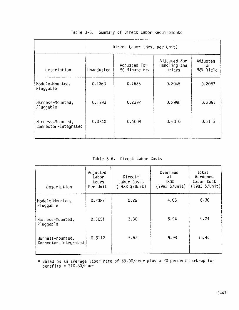
Table 3-5. Summary of Direct Labor Kequirements
Direct Labor (Hrs. per Unit)
Adjusted For Adjusted Adjusted For Handling and For
Description Unadjusted 50 Minute Hr. Delays 98"~ Yield
Module-Mounted, 0.1363 0.1636 0.2045 0.2087 Pluggable
Harness-Mounted, 0.1993 0.2392 0.2990 0.3051 Pluggable
Harness-Mounted, 0.3340 0.4008 0.5010 0.5112 Connector-Integrated
Table 3-6. Direct Laoor Costs
Adjusted Overhead Total Labor Direct* at Burdened Hours Labor Costs 180% Labor Cost
Description Per Unit (1983 $/Unit) (1983 $/Unit) (1983 $/Unit)
Module-Mounted, 0.2087 2.25 4.05 6.30 P1uggao1e
Harness-Mounted, 0.3051 3.30 5.94 9.24 Pluggable
Harness-Mounted, 0.5112 5.52 9.94 15.46 Connector-Integrated
* Based on an average labor rate of $9.00/hour plus a 20 percent mark-up for benefits = $10.80/hour
3-47
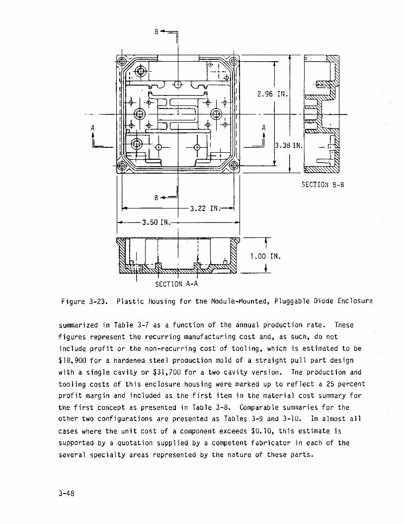
B
2.96·-IN.
A
L 3.38 IN.
! SECTION 8-B
t---- 3.50 I N.--t----------i
t 1 .00 IN.
+
Figure 3-23. Plastic Housing for the Module-Mounted, Pluggable Diode Enclosure
summarized in Table 3-7 as a function of the annual production rate. These figures represent the recurring manufacturing cost and, as such, do not include profit or the non-recurring cost of tooling, which is estimated to be
$18,900 for a hardened steel production mold of a straight pull part design with a single cavity or $31,700 for a two cavity version. The production and
tooling costs of this enclosure housing were marked up to reflect a 25 percent profit margin and included as the first item in the material cost summary for
the first concept as presented in Table 3-8. Comparable summaries for the other two configurations are presented as Tables 3-9 and 3-10. In almost all
cases where the unit cost of a component exceeds $0. 10, this estimate is supported by a quotation supplied by a competent fabricator in each of the several specialty areas represented by the nature of these parts.
3-48
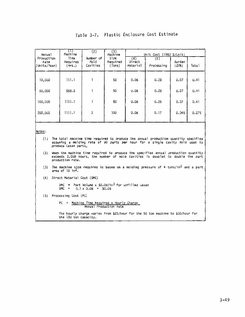
Table 3-7. Plastic Enclosure Cost Estimate
Annual II !
r'lachi ne (2) (3)
Unit Cost (1983 $/Unit) I'lachine Proouction Time Number of Size (4) (5)
Kate Required Mold Required Ui rect Burden (Units/Year) (Hrs.) Cavities (Tons) I'lateri a 1 Processing (20%) Total
10,000
50,000
100,000
200,000
~:
(1)
1ll.1 1 50 0.06 0.28 0.07 U.41
555.5 1 50 U.06 0.28 0.07 0.41
1111.1 1 50 0.06 0.28 0.07 0.41
1111.1 2 100 0.06 0.17 0.045 0.275
The total machine time required to produce the annual production quantity specif.ieo assuming a molding rate of 90 parts per hour for a single cavity mold used to produce Lexan parts.
(2) When the machine time required to produce the specifieo annual production quantity exceeds 2,000 hours, tne number of mold cavities is doubled to double the part production rate.
(3)
(4)
The machine size required is based on a molding pressure of 4 tons/in 2 and a part area of 10 in 2•
Direct Material Cost (OMC)
UMC = Part Volume x $0.08/in 3 for unfilled Lexan UMC = 0.7 x 0.08 = $0.06
(5) Processing Cost (PC)
PC = Machine Time Required x Hourly.Charge Annual Production Rate
The hourly charge varies from $25/hour for the 50 ton maChine to $30/hour for the 100 ton capacity.
3-49
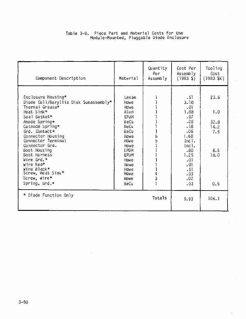
Table 3-8. Piece Part and Material Costs for the Module-Mounted, Pluggable Diode Enclosure
Qu ant i ty Cost Per Per Assembly
Component Description Materi a 1 Assembly (1983 $)
Enclosure Housing* Lexan 1 .51 Diode Cell fBeryll i a Disk Subassembly* Howe 1 3.10 Therma 1 Grease* Hdwe 1 .01 Heat Si nk* Alum 1 1.88 Seal Gasket* EPlJM 1 .07 Anode Spring* BeCu 1 .28 Ca thode Spri ng* BeCu 1 • 18 Grd. COntact*' BeCu 1 .06 Connector Housing Hdwe 6 1.68 Connector Terminal Hdwe :, Inc 1. Co nnector Grd. Howe 1 Inc l. Boot Hous i ng EPDr~ 1 .80 Boot Ha rness EPDM 1 1.25 Wi re Grd. * Howe 1 .01 Wire Red* Hdwe 1 .01 Wi re Black * Hdwe 1 .01 Screw, Heat Sink* Hdwe 4 .03 Screw, Wire* Howe 3 .02 Spring, Grd.* BeCu 1 .03
* Diode Function Only Totals 9.93
3-50
Tooling Cost
(1983~K)
23.6
1.0
, 32.8 14.2
7.5
l 8.5 18.0
i
0.5
106. 1
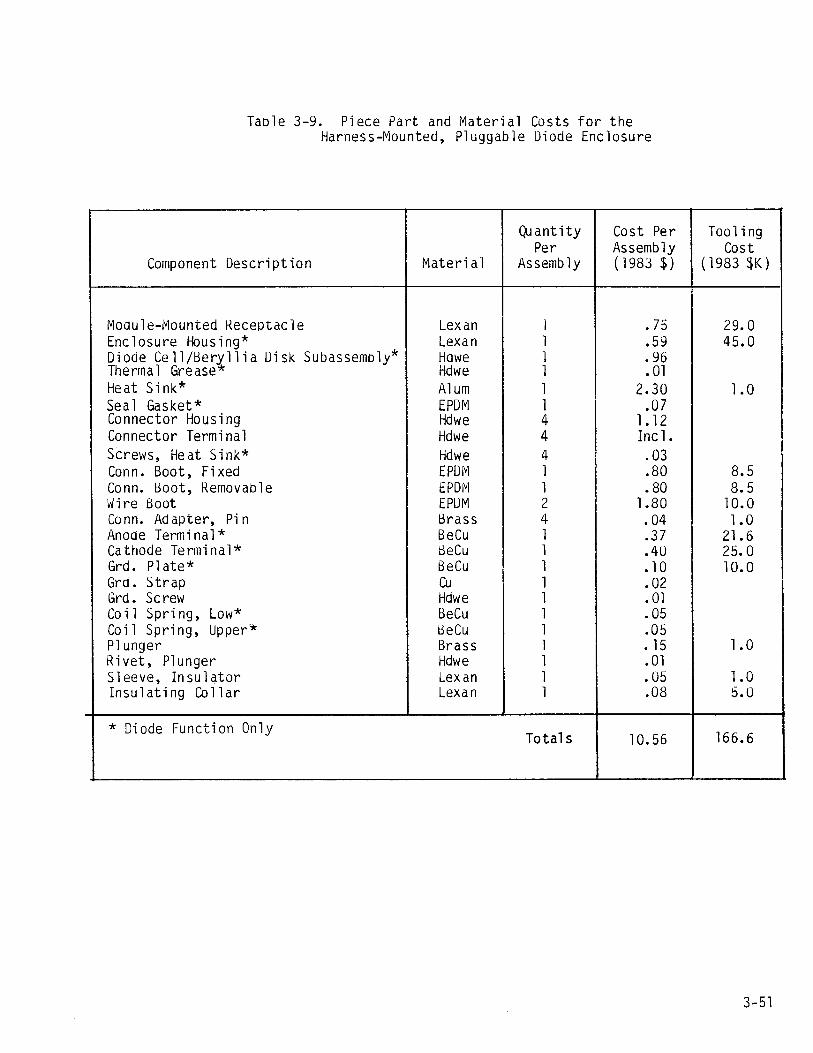
Table 3-9. Piece Part and Material Costs for the Harness-Mounted, Pluggable Diode Enclosure
Qu ant i ty Cost Per Per Assembly
Component Description Material Assembly (1983 $)
Module-Mounted Receptacle Lexan 1 .75 Enclosure Housing* Lexan 1 .59 Diode Cell/~eryllia Disk Subassembly* Hdwe 1 .96 Therma 1 Grease* Hdwe 1 .01 Heat Si nk* Alum 1 2.30 Sea 1 Gasket * EPOM 1 .07 Connector Housing Hdwe 4 1. 12 Connector Terminal Hdwe 4 Inc 1. Screws, He at S i nk* Hdwe 4 .03 Conn. Boot, Fixed EPOM 1 .80 Conn. boot, Removable EPDfvl 1 .80 Wire Boot EPUM 2 1.80 Conn. Adapter, Pi n Brass 4 .04 Anode Terminal* BeCu 1 .37 Cathode Terminal* t3eCu 1 .40 Grd. Pl ate* BeCu 1 .10 Grd. Strap Cu 1 .02 Grd. Screw Hdwe 1 .01 Co il Spri ng, Low* BeCu 1 . 05 Coi 1 Spring, Upper'* BeCu 1 .05 Plunger Brass 1 . 15 Rivet, Pl unger Hdwe 1 .01 Sleeve, In su 1 ator Lexan 1 .05 Insulating Collar Lexan 1 .08
* Diode Function Only Totals 10.56
Tool i ng Cost
(1983 $K)
29.0 45.0
1.0
I
8.5 8.5
10.0 1.0
21.6 25.0 10.0
1.0
1.0 5.0
166.6
3-51
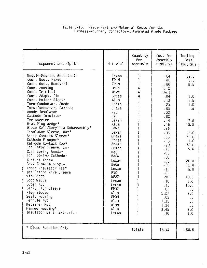
Table 3-10. Piece Part and Material Costs for the Harness-Mounted, Connector-Integrated Diode Package
Quant i ty Cost Per Per Assembly
Component Description Material Assembly (1983 $)
Module-Mounted Keceptacle Lexan 1 .84 Conn. ~oot, Fixed EPDM 1 .80 Conn. Boot, Removable EPDM 1 .80 Conn. Hous i ng Hdwe 4 1. 12 Conn. Term; na 1 Hdwe 4 Inc 1. Conn. Adapt. Pin Brass 4 .04 Conn. Holder Sleeve Alum 1 .13 Thru-Conductor, Anode Brass 1 .05 Th ru- Co ilductor, Ca thode Brass 1 .05 Anode Insulator PVC 1 .02 Cathode Insulator PVC 1 • 02 Tee l:3arrier Lexan 1 • 14 Heat Pl ug Wedge* Alum 1 • 16 Di ode Ce 11 /Be ry 11 i a Subassemb 1 y-* Hdwe 1 .96 Insulator Sleeve, Out* Lexan 1 .05 Anode Contact' Sleeve* Brass 1 .35 Cathode Plunger* Brass 1 • 15 Cathode Contact Cup*" Brass 1 .20 Insulator Sleeve, In* Lexan 1 • 10 Coil Spring Anode* BeCu 1 .06 Coil Spring Cathode* BeCu 1 .06 Contact Cage* Lexan 1 .28 Grd. Contact Assy.* BeCu 1 .20 Inner Insulator Tee"" Lexan 1 • 12 Insulating Wire Sleeve PVC 1 .01 Wire Boot EPDM 1 .90 l:3oot Wedge Lexan 1 • 10 Outer Nut Lexan 1 .15 Seal, Plug Sleeve EPD~l 1 .02 Plug Sleeve Alum 1 2.27 Seal, Housing EPDM 1 .02 Ferrule Nut Alum 1 1.35 Retainer Nut Alum 1 1.34 Finned Housing'* Alum 1 3.45 Insulator Liner Extrusion Lexan 1 .10
* D'i ode Function Only Totals 16.41
3~2
Tooling Cost
(1983~K)
32.5 8.5 8.5
1.0 1.5 1.0
.5
7.0 10.0
5.0 20,0 1.0
10.0 5.0
20.0 12.0 5.0
10.0 5.0
10. a .5
2.0 .5 .5 .5
2.0 1.0
180.5
As might be expected, the total material cost for each concept is
directly related to the number of separate piece parts in each assemoly. This
relationship is somewhat distorted by the change in the configuration of the diode cell/berylli.a diode subassemoly which occurs between the first concept and the other two. In the former case, where leaf springs are used to electrically contact the diode cell/beryllia disk assembly, a larger diameter BeO disk is required to allow for the necessary dielectric barrier between the anode and cathode spring contacts. The effect of this parameter on the cost
of the diode cell/Deryllia disk subassembly is illustrated in Table 3-11. The
leaf spring contacting system used in the "module-mounted, pluggable" concept requires a 0.813 inch diameter BeO disk with an associated subassembly price of $3.10 as detailed in the first column of this table. The concentric
plunger contacting approach used in the other two reference designs enables
the BeO disk diameter to be reduced to a 0.50 inches with a dispropor
tionately large decrease in the disk cost due to the reasons discussed in Section 3.3.2.2.1.
3.3.3.4 Production Cost Summary
The FOB factory cost of producing each of the three reference bypass diode enclosure designs was estimated by combining the direct labor and overhead costs from Section 3.3.3.2 with the material costs from Section 3.3.3.3 to yield the results summarized in Table 3-12. It should be
noted that the special tooling costs have been amortized using a 25 percent
capital recovery factor with an annual production rate of 37,500 units. This production rate is consistent with the 50,000 m2 of annual module production and with a bypass diode installation which is capable of operating with 30
amperes of rated source circuit current. If we assume a module efficiency of
10 percent, these estimated FOB factory prices can be transformed into an equivalent price per unit of peak power to yield values of $0.16, $0.20, and
$0.31/watt for each of the three concepts in the order listed in Table 3-12.
To permit comparison with other diode packaging approaches, the
bypass diode costs and the module electrical termination costs must be separated. The direct labor costs and material costs for the bypass diode
3-53
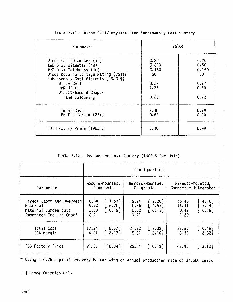
Table 3-11. Diode Ce11/Bery1Jia Disk Subassembly Cost Summary
Parameter V·a 1 ue
Diode Cell Diameter (in) 0.22 0.20 BeD Disk Diameter (in) 0.813 0.50 BeO Disk Thickness (in) 0.150 0.150 Diode Reverse Voltage Rating (volts) Subassembly Cost Elements (1983 ~)
50 50
Di ode Cell 0.37 0.27 Be~ DisL ._. 1.85 0.30 Direct-Bonded Copper
and Soldering 0.26 0.22
Total Cost 2.48 0.79 Profi t i-1arg i n (25%) 0.62 0.20
FOB Factory Price (1983 ~) 3.10 0.99
Table 3-12. Production Cost Summary (1983 $ Per Unit)
Configuration
Modu1e-J't1ounted, Harness-Mounted, Harness-Mounted, Parameter Pluggable Pluggable Connector-Integrated
Direct Labor and Overhead 6.30 . [ 1.57J 9.24 L 2.20J 15.46 [ 4.16J I Material 9.93 [ 6.20J 10.56 [ 4.Y3J 16.41 [ 6.14J Material Burden (3%) 0.30 [ 0.19J 0.32 [ 0.15J 0.49 [ 0.18J Amortized Tooling ·Cost* 0.71 1. 11 1.20
Total Cost 17.24 L 8.b7J 21.23 [ 8.39] 33.56 [1O.48J 25% Margin 4.31 [ 2.17J 5.31 [ 2.10J 8.39 [ 2.62J
FOB Factory Price 21. 55 [10.84] 26.54 [1O.49J 41.95 [13.10J
* USing a 0.25 Capital Recovery Factor with an annual production rate of 37,500 units
[ J Diode Function Unly
3-54
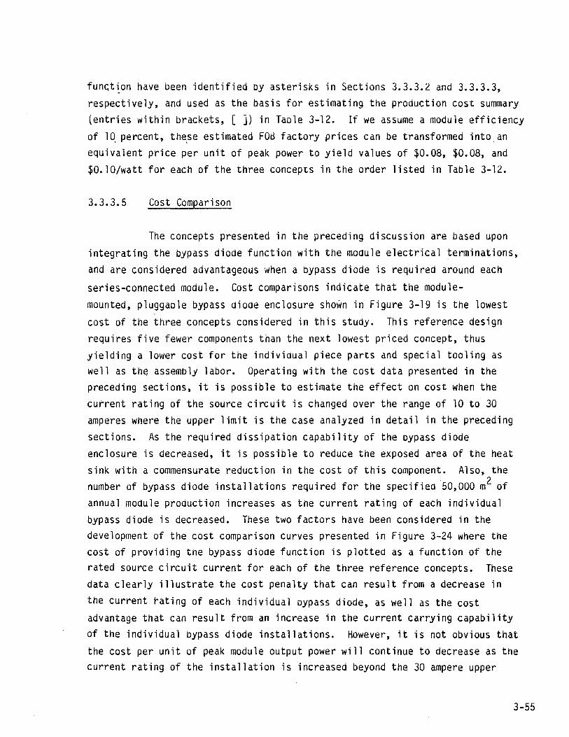
fun~tton have been identified by asterisks in Sections 3.3.3.2 and 3.3.3.3, respectively, and used as the basis for estimating the production cost summary (entries within brackets, [ J) in Table 3-12. If we assume a module efficiency
of 10 percent, these estimated FO~ factory prices can be transformed into an . , .
equivalent price per unit of peak power to yield values of $0.08, $0.08, and $O.lO/watt for each of the three concepts in the order listed in Table 3-12.
3.3.3.5 Cost Comparison
The concepts presented in the preceding discussion are based upon
integrating the bypass diode function with the module electrical ~erminations,
and are considered advantageous when a bypass diode is required around each
series-connected module. Cost comparisons indicate that the module-
mounted, pluggable bypass diode enclosure shown in Figure 3-19 is the lowest
cost of the three concepts considered in this study. This reference design requires five fewer components than the next lowest priced concept, thus yielding a lower cost for the individual piece parts and special tooling as well as the assembly labor. Operating with the cost data presented in the preceding sections, it is possible to estimate the effect on cost when the current rating of the source circuit is changed over the range of 10 to 30 amperes where the upper limit is the case analyzed in detail in the preceding
sections. As the required dissipation capability of the bypass diode enclosure is decreased, it is possible to reduce the exposed area of the heat sink with a commensurate reduction in the cost of this component. Also, the number of bypass diode installations required for the specified 50,000 m2 of annual module production increases as the current rating of each individual bypass diode is decreased. These two factors have been considered in the development of the cost comparison curves presented in Figure 3-24 where the cost of providing the bypass diode function is plotted as a function of the rated source circuit current for each of the three reference concepts. These data clearly illustrate the cost penalty that can result from a decrease in
the current rating of each individual oypass diode, as well as the cost advantage that can result from an increase in the current carrying capability of the individual bypass diode installations. However, it is not obvious that
the cost per unit of peak module output power will continue to decrease as the current rating of the installation is increased beyond the 30 ampere upper
3-55
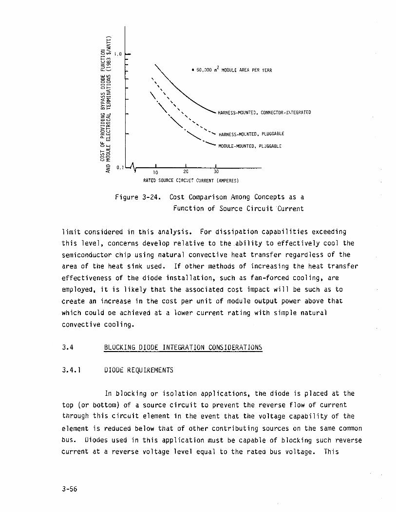
U.J V1 OZ 00 .......... O~
eo: V1 ;;:: V1 ..... eo:::;: c.. cr: >- U.J <Xl ~
t!) ~ Zeo: ..... U 0 ..... ..... cr: >~ OU cr: U.J c.. ~
U.J u.. o U.J ~
~:::> V1 0 00 U::;:
, • 50,JOO m2 MODULE AREA PER YEAR
. , " '" , .... "" "'" . .."
HARNESS-MOUNTED, CONNECTOR-INTEGRATED
~ ',- HARNESS-MOUNTED, PLUGGABLE
'~ MODULE-MOUNTED, PLUGGABLE
~ 0.1 <I:
RATED SOURCE CIRCUIT CURRENT (AMPERES)
Figure 3-24. Cost Comparison Among Concepts as a Function of Source Circuit ·Current
limit considered in this analysis. For dissipation capabilities exceeding this level, concerns develop relative to the ability to effectively cool the semiconductor chip using natural convective heat transfer regardless of the area of the heat sink used. If other methods of increasing the heat transfer effectiveness of the diode installation, such as fan-forced cooling, are employed, it is likely that the associated cost impact will be such as to create an increase in the cost per unit of module output power above that which could De achieved at a lower current rating with simple natural convective cooling.
3.4 BLOCKING DIODE INTEGRATION CONSIDERATIONS
3.4.1 DIODE REQUIREMENTS
In blocking or isolation applications, the diode is placed at the top (or bottom) of a source circuit to prevent the reverse flow of current through this circuit element in the event that the voltage capability of the
element is reduced below that of other contributing sources on the same common bus. Diodes used in this application must be capable of blocking such reverse current at a reverse voltage level equal to the rated bus voltage. This
3-56
situation could exist if the voltage contribution from the affected source
circuit is reduced to zero by an internal failure such as a short to ground at the top of the circuit.
It is possible to use the same generic diode for this application with the appropriate specification of reverse voltage rating. As shown in Figure 3-25, the unit price for such devices will increase as the required
r~verse voltage rating is increased. While all devices of this type are inherently capable of blocking in excess of 1000 volts as a rated reverse voltage, this pricing structure reflects the reduced yield of devices with the higher rev'erse voltage capabilities.
1. 00
o.ao -~ 0.60
""" -z: :::l 0.40
0.2
.100,000 UNITS
-- ...... t--
__ -i --- ,/
/
/ /
'"
/ +/
........ "', ./
'"
......
.....
DIODE CELL DIA/CURRENT RATING·
/~ 0.220 In/50A
,t O. 2 a a i n /4 a A
0.140 in/20A
a ~ ______ ~ ______ ~ ______ ~ ______ ~ ______ ~ ______ __ a 200 400 600 aco 100(1
REVERSE VOLTAGE'RATING (VOLTS)
Figure 3-25. Diode Cell Unit Price as a Function
of keverse Voltage Rating
3-57
3.4.2 CIRCUIT PROTECTION
Article 690 of the 1984 National Electrical Code will require the use of a source circuit·overcurrent device when this circuit is corinected to
more than one electrical source and when the ampacity of the conductors in the source circuit is less than the maximum available current under short-circuit or ground-fault conditions with a shorted blocking diode. Thus, the inclusion of a fuse with the blocking diode is indicated for the general case where the array is configured as the parallel connection of multiple source circuits. When used for source circuit overcurrent protection, the fuse must be accessible, but is not required to be readily accessible.
Fuses are usually rated in terms of rms values assuming ac operation at 60 Hz. For dc applications, the rated voltage must be adjusted as illustrated in Figure 3-26 for typical semiconductor fuses. For a short-circuit L/R time constant of 10 milliseconds or less, all fuses in this series will have a dc voltage rating which is at least as high as the ac voltage rating. Fuse current ratings are given in ac (rms) amperes for an ambient temperature of 200 C. Good design practice dictates the use of a temperature derating factor as illustrated in Figure 3-27 for a typical semiconductor fuse. Thus, for operation in a still air ambient at 800 C, which is not unrealistic for a source circuit protection device housed in an enclosure along with a olocking diode, the fuse should be derated to 70 percent of its rms current rating.
For the protection of the photovoltaic source circuit wiring, including the internal mOdule connections, the 12t let-thru of the .fuse must be less than the 12t withstand of the circuit conductors. Under ground-fault conditions whiCh could lead to the heating of source circuit conductors, the ultimate conductor temperature depends on (1) the magnitude of the fault current, (2) the cross-sectional area of the conductor, (3) the duration of
3-58
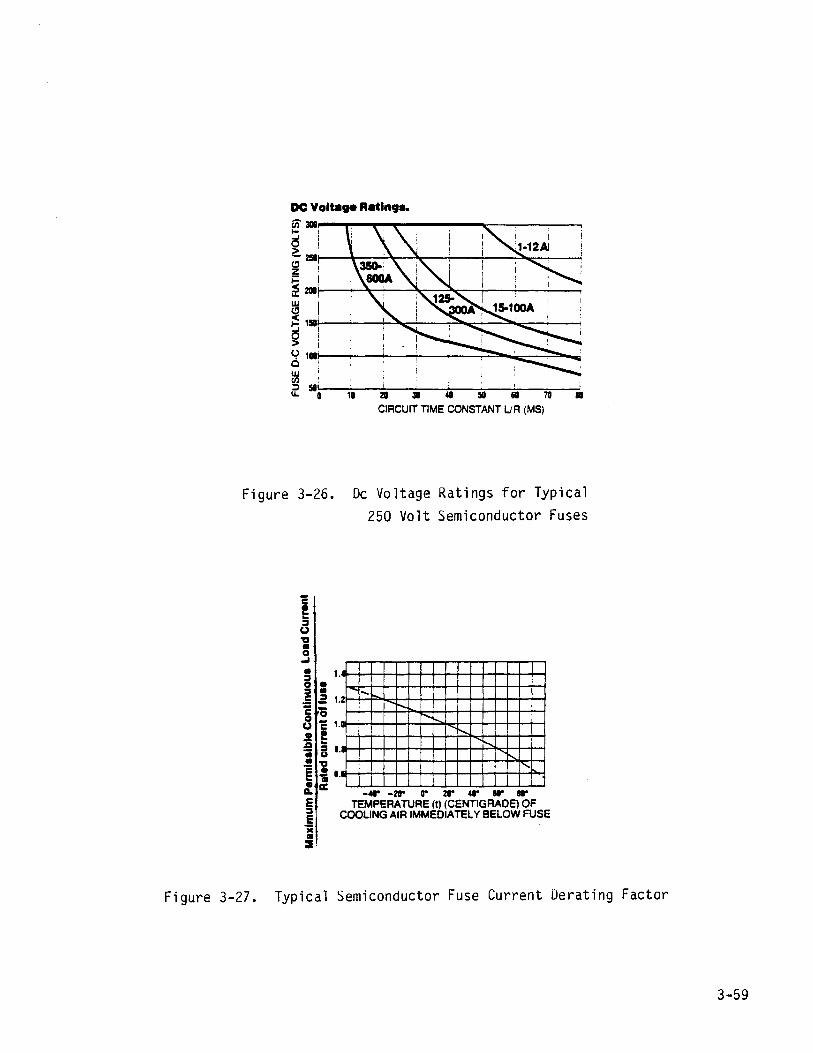
Figure 3-26. Dc Voltage Ratings for Typical 250 Volt Semiconductor Fuses
I .. :=I
Co)
" • .3 • :=I o • :=I • .5 .= t Co 8 c t
• ! ;e ~ • • u i 1 D .. . .f~ E :=I E .. • :I
-.2 ,.... r"'-
.D t-......
I'-....
......
- .... -20" go 20" .... II" II" TEMPERATURE (tl (CENTIGRADE) OF
COOLING AIR IMMEDIATELY BELOW FUSE
Figure 3-27. Typical Semiconductor Fuse Current Derating Factor
3-59
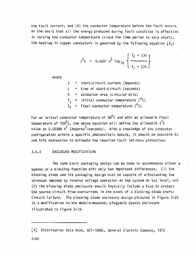
the fault current, and (4) the conductor temperature before the fault occurs. On the basis that all the energy produced during fault condition is effective in raising the conductor temperature (since the time period is very short),
the heating in copper conductors is g9verned, by the following equation [4J:
+ 234}
+ 234
Where I = short-circuit current (Amperes) t = time of short-circuit (seconds) A = conductor area (circular mils)
Ti = initial conductor temperature (oC)
Tf = final conductor temperature (oC)
For an initial conductor temperature of 500 C and with an allowable final temperature of 150oC, the above equation will defjne the allowable I2t value as 0.00389 A2 (Amperes 2-seconds). With a knowledge of the conductor configur4tion within a specific photovoltaic module, it should be possiole to use this expression to estimate the required fault let-thru protection.
3.4.3 ENCLOSURE MODIFICATIONS
The same basic packaging design can be made to accommodate either a bypass or a blocking function with only two important differences: (1) the blocking diode and its packaging design must be capable of withstanding the stresses imposed by reverse voltage operation at the system dc bus level, and (2) the blocking diode enclosure should logically include a fuse to protect the source circuit from overcurrent in the event of a blocking diode shortcircuit failure. The blocking diode enclosure design pictured in Figure 3-28 is a modification to the module-mounted, pluggaole bypass enclosure
illustrated in Figure 3-19.
[4J Distribution Data Book, GET-1008l, General Electric Company, 1972
3-60
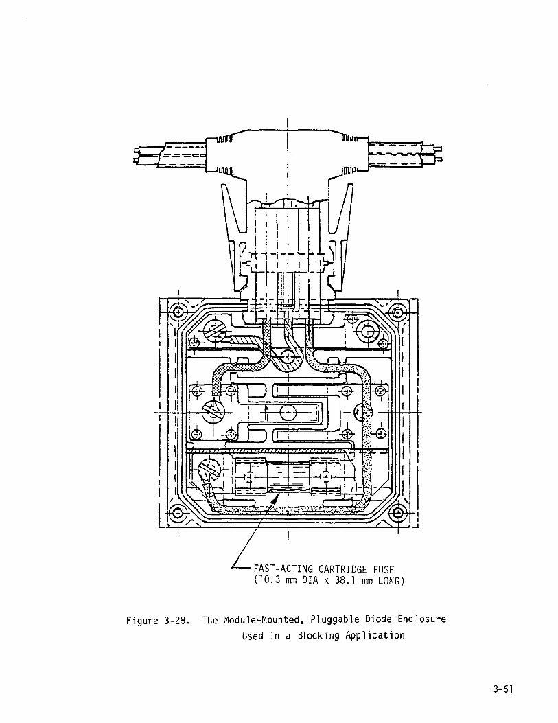
FAST-ACTING CARTRIDGE FUSE (10.3 mm DIA x 38.1 mm LONG)
Figure 3-28. The Module-Mounted, Pluggable Diode Enclosure Used in a Blocking Application
3-61
As shown in Figure 3-29, the molded plastic box has been designed
to accommodate either application. The formed metal parts which are mounted
within the interior of this box must be customized to the application as shown
on the left-hand side of the figure. This modification consists 'of a change in the configuration of the anode and cathode contact spring plate to accommodate a pair of fuse clips. The fuse is housed in the portion of the box that was formerly dedicated to the attachment of the ribbon leads from the module to the diode anode and cathode contact plates. In a blocking diode application, the enclosure can be mounted to any convenient surface since there are no required interconnections through the bottom of the box. When
the blockin9 diode enclosure is plugged into a moaule-to-module wiring harness containing one more connector than the number of series-connected modules in the source circuit, the source circuit is protected by an isolation diode in series with a fuse.
In a similar fashion, it is possible to modify the harness-mounted, pluggable diode enclosure shown in Figure 3-20 to adapt to a blocking application as illustrated in Figure 3-30. Again, the molded plastic box and diode mounting arrangement are identical for either application with the
changes being affected via the formed metal contacts within the box.
3.4.4 COST IMPLICATIONS
The cost implications of converting the two previously described enclosures from a bypass to a blocking dioae function were analyzed based on the definition contained in Section 3.4.3 under the assumption that the enclosures are being produced to satisfy the bypass diode application in the
quantities required for 50,000 m2 of module area per year (37,500 units per
year with a 30 ampere current rating) ana that it is desired to augment this
production to include an additional 950 enclosures per year which are modified to accommodate the blocking function. Under these conditions, Table 3-13 represents the total annual cost for each enclosure design approach when
considerea as two production scenarios: (1) bypass enclosures only, and (2) bypass enclosures plus blocking enclosures. The cost of the blocking
3-62
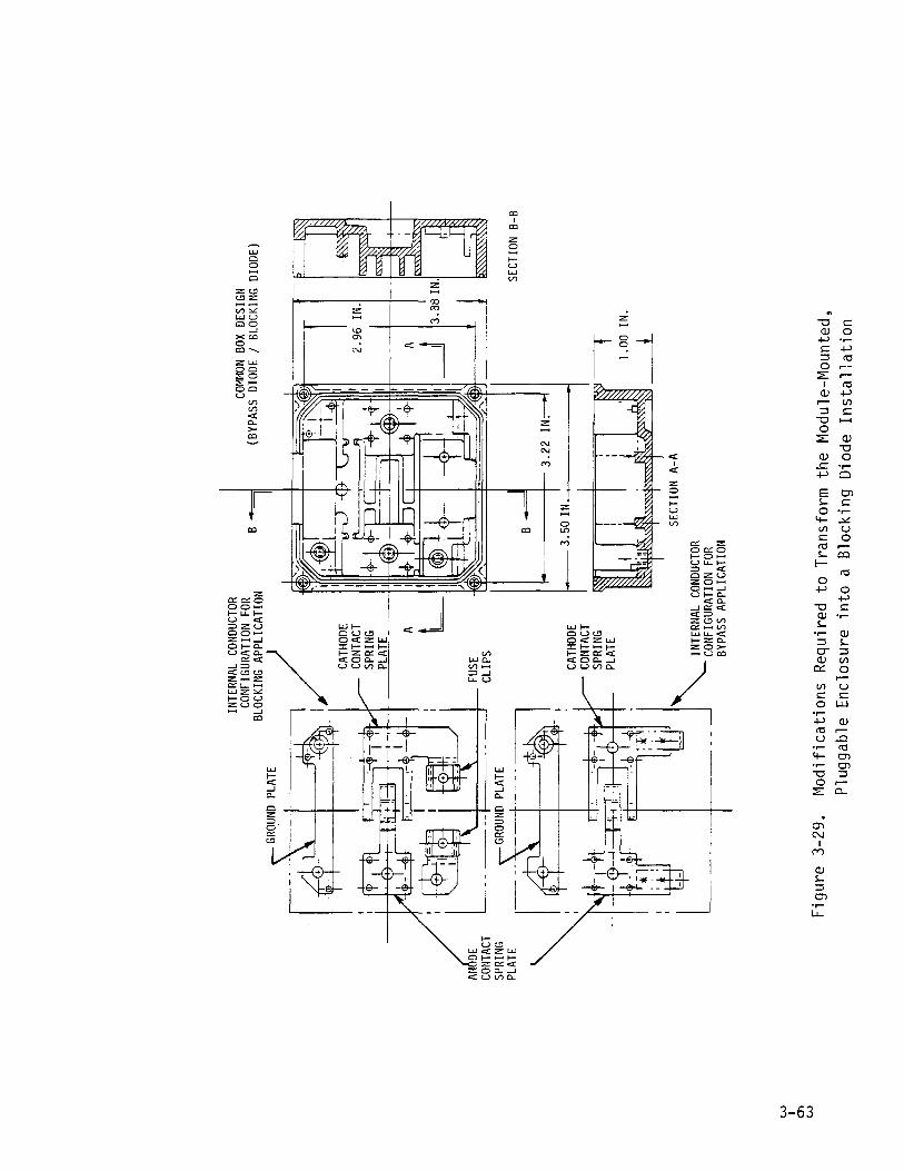
W
I m
w
INTE
RNAL
CO
NDUC
TOR
CONF
IGUR
ATIO
N FO
R BL
OCKI
NG A
PPLI
CATI
ON
B
I Co
r~MO
N BO
X DE
S I GN
(B
YPAS
S DI
ODE
/ BL
OCKI
NG D
IODE
)
GROU
ND P
LATE
/
r-=-
-'~~
r-~l
-l
I ~
~t-
CATH
ODE
I .
I CO
NTAC
T I
-f~-
.-4>\
I:'
.=4--;
~l-
SPRI
NG
__
PLAT
E_
r-1Hm
l
L ~ ~ __ :::::
l ~mS
A
~
--
,>-"
I.~
B
----+
-3.
22
IN.
~~::~~
i 1
3
_ SO
'" !
["~:,"
.I~
~r!
im:' 14U~~~IN-
. _
_ L
I •• j
:,c:5:"
"" ~"
I
SECT
ION
A-A
"'-
I NTE
RNAL
CO
NDUC
TOR
CONF
IGUR
ATIO
N FO
R BY
PASS
APP
LICA
TION
Fig
ure
3-29
. M
odif
icat
ions
R
equi
red
to T
rans
form
the
Mod
ule-
Mou
nted
, P
lugg
able
E
nclo
sure
in
to a
Blo
ckin
g D
iode
In
stal
lati
on
SECT
ION
B-B
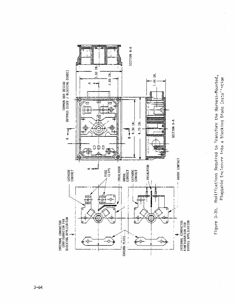
W I 0'1 ~
INTE
RNAL
CON
DUCT
OR
CONF
IGUR
ATIO
N FO
R BL
OCKI
NG A
PPLI
CATI
ON
t ~~~~
CATH
ODE
CONT
ACT
B, CO
f4MON
BOX
DES
IGN
(BYP
ASS
DIOD
E I
BLOC
KING
DIO
DE)
3.50
IN
.
I
~--
\ -_
_ I
4 IN
TERN
AL C
ONDU
CTOR
CO
NFIG
URAT
ION
FOR
BYPA
SS A
PPLI
CATI
ON
FUSE
CL
IPS
INSU
LATO
R AN
ODE
CONT
ACT
CATH
ODE
CONT
ACT
INSU
LATO
R
ANOD
E CO
NTAC
T
f i-
-+
-1
.44
IN
.
SECT
ION
A-A
Fig
ure
3-30
. M
odif
icat
ions
R
equi
red
to T
rans
form
the
Har
ness
-Mou
nted
, P
lugg
able
Enc
losu
re
into
a B
lock
ing
Dio
de Insta'l~tion
SECT
ION
B-B
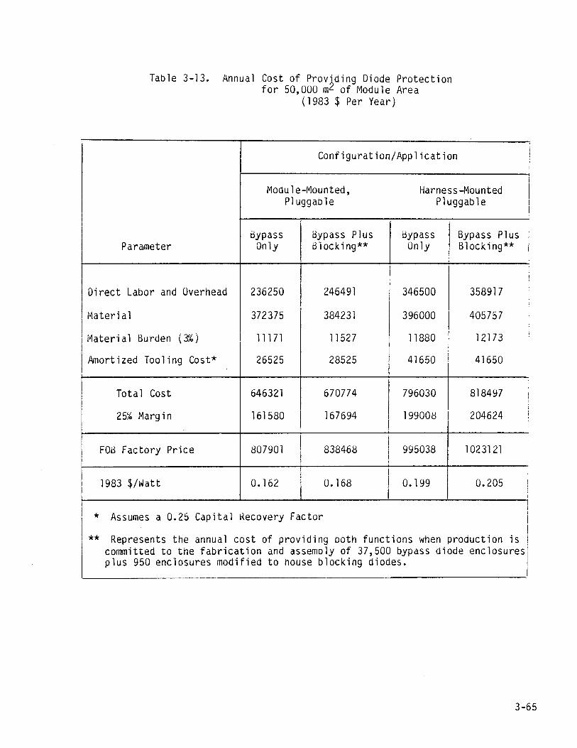
Table 3-13. Annual Cost of Providing Diode Protection for 50,000 m2 of Module Area
(1983 $ Per Year)
Configuration/Application
Module-Mounted, Harness-Mounted Pluggable Pluggable
I
Bypass Bypass Plus Bypass Bypass Plus I I I
Parameter Only Blocking** Only Blocking** I ,
, I i
Direct Labor and Overhead 236250 246491 346500 358917
Materi a 1 372375 384231 396000 405757
Materi a 1 Bu rden (3"") 11171 11527 11880 12173 i
t
I
Amortized Tooling Cost* 26525 28525 41650 41650 I
Total Cost 646321 670774 796030 818497 ,
,
25% Marg i n 161580 167694 I 1990013 204624 i
FOB Factory Price 807901 8384613 995038 1023121
i
1983 $/Watt 0.162 0.168 0.199 0.205 ! , i
i * Assumes a 0.25 Capital Recovery Factor i
I
I ** Represents the annual cost of providing both functions when production is I
committed to the fabrication and assemoly of 37,500 bypass diode enclosures
l plus 950 enclosures modified to house blocking diodes.
3-65

diode modification includes the fuse, the increased cost associated with the acquisition of diodes with a 1000 volt reverse voltage rating as well as changes to the internal wiring of the enclosure.
When the annual FOB factory price of each approach is expressed as
a cost per unit of peak module output, it is not surprising that the inclusion
of a blocking diode enclosure in the ratio of approximately 1 for every 40
bypass diode enclosures will increase the cost per unit of peak power output by about this same ratio; slightly more for the mOdule-mounted, pluggable enclosure since the unit cost is higher due to the inclusion of the fuse and
the higher reverse voltage rated diode and slightly less for the harnessmounted, pluggable enclosure since the elimination of the connector contacts
more than offsets the increases due to the aforementioned additions.
3-66
SECTION 4
CUNCLUSIONS AND RECUMMENDATIONS
Diodes, used in both bypass and blocking applications, are vital components in any terrestrial photovoltaic array. However, when used in the bypass mode, where the numoer of such diodes is proportional to the area of
the array, the cost of providing this function and the module terminations, as
determined by this design study and analysis, is approximately $0.16 per watt
of peak module output power (in 1983 $). As the cost of photovoltaic modules
continues to decline, this cost oecomes an increasing fraction of the total
installed cost of the array. At a mOdule price level which would make
photovoltaic generation a viable option for a central station power plant, the
cost of integrating the bypass diode function and the module electrical
termination could be prohibitively high unless steps are taken to reduce the number of diodes required per unit area of array. This reduction can be accomplished by increasing the current carrying capacity of each bypass diode installation or by increasing the number of series-connected solar cells in each bypassed group. The implementation of the former approach is limited by the ability to maintain the diode junction temperature within acceptable
limits as the device dissipation is increased under worst-case ambient conditions, including high air temperature with zero wind speed. Under these
conditions, the effectiveness of the heat transfer can be increased by forced air or liquid cooling, but the cost and reliability impact of such approaches would probably overshadow any cost improvement resulting from the reduced requirement for diode installations within the array.
with respect to increasing the number of series-connected solar cells in
each bypassed group, this option does not impact the power dissipation capability of the bypass diode with the associated cost consequences cited above, but it does create concerns relative to "hot-spot" heating within the
larger bypassed group. The potential for such heating must be carefully evaluated using the actual reverse voltage characteristics of the solar c~lls and considering the impact of various cell failures as well as any probable
shadowing conditions.
4-1