Embed Size (px)
Citation preview

Digital Voltmeter
I. IntroductionOur goal here is to build a voltmeter. We will do this using almost all digital circuitry
rather than analog. The circuit works like many other digital measurement circuits in that itconverts the quantity to be measured into a time interval, then measures that time.
Call the voltage we wish to measure Vin. Say we charge a capacitor linearly with time(that is, at a constant charging current I), starting at zero volts. It will take a time t = Vin/ (dVin /dt) = Vin C / (dQ / dt) = Vin C / I for the capacitor to charge up to Vin. So if we can measure thistime interval, we can determine Vin. To measure time in digital electronics, we produce a highfrequency pulse train and count the pulses occurring during the time interval to be measured.The number of pulses counted is a measure of the time interval, and hence of Vin. With somesuitable conversion and a display, this makes a digital voltmeter (DVM).
To realize this idea with actual circuit elements (mostly integrated circuits or IC's) werequire a number of separate sections. The complete circuit diagram for the eventual project isshown on the last page of this writeup (don't let it frighten you!). On the secondtolast page isthe same circuit with its functional sections outlined and labeled. The sections needed for thisproject are:A) A pulse train generator. In electronics, this is called a clock. We have already learned how
to build this using the 555 timer chip. This is the clock generation section.B) A way to monitor the voltage across the capacitor and generate signals when the
charging starts at zero volts and when the voltage becomes equal to the voltage to bemeasured, Vin. I call this the section control and gating.
C) A way to “count” the number of clock pulses that occur between the start and stopcharging signals. This is the counting section.
D) A constant current capacitor charging circuit that can be turned on and off and reset tozero volts by the start and stop charging signals. analog input/transducer
E) A humanreadable way to display the number of pulses counted during this interval. This isthe latching and display section.
We will learn how to build each of these sections, then connect them together into thefunctioning DVM.
II. SectionbySection BuildUpSo, let us get started. A. Clock Generation Part A we already have learned to do in the previous lab. Digital things, though, prefer to workat 0 or 5V. Therefore, either power the 555 from 5V instead of 10 or 15V (see spec sheet), or putpin three on a voltage divider to bring the output down to 5V. This is the method chosen in thefinal schematic at the end
B. Basic Control and GatingTo carry out the function of Part B we use a solution based on an integrated circuit called
a comparator. The entire purpose of this IC is to signal which of two voltages is larger. One ofthe voltages will be Vin and the other will be the voltage across the capacitor. The comparatorhas to do its job without drawing any appreciable current, otherwise it will interfere with theconstantcurrent charging. To achieve nearzero input current we will use a LF355 FETinput
1

opamp as our comparator.We will discuss opamps in detail in class. For now, we can just learn that the opamp is
a chip with two inputs labeled + and – (with the voltages at these points called V+ and V) andcalled the noninverting and inverting inputs. It has just one output. Of course like any IC itrequires power and ground connections, in this case two power supplies (Vcc = +10V and Vee =10V—these are just conventional names for the power voltages).
If the voltage at the + input is greater (more positive) than the voltage at the – input (V+
> V), the 355 will drive its output high, near to Vcc. If the opposite becomes true, (V > V+), theoutput will go low, near to Vee.
Just for this part of the lab, we will use a couple of LED's to monitor the state of the opampoutput. The LED is symbolized by:
and is a Light Emitting Diode. We discussed diodes generally in class. They act as one way valves for current. The
arrow points in the direction conventional (positive) current is allowed to flow. The shorter leadwire on an LED corresponds to the tip of the arrow. (For historical reasons this side is alsocalled the cathode; the other side of the device is called the anode.) When the diode is “biased”(i.e. voltage is applied) to conduct in this direction, it is said to be forward biased.
If you forward bias these LED's with less than about 1.6 Volt, little current flows and nolight is produced. On the other hand, if you try to cause a larger forward voltage drop across adiode, you will find that you won't be able to do it. Any diode will always “try” to maintain acertain voltage drop of about 1 Volt across itself (see below for details on the exact value). Thediode will keep its forward bias voltage drop constant by drawing more and more current fromthe power supply until either the supply sags or the diode burns up. The exact value of theforward bias voltage drop depends on the material the diode is made of and nothing else. RedLED's are made of gallium arsenide (GaAs), a manmade material that does not exist in nature.They have a forward bias voltage of about 1.6 volts and they only emit light when the forwardbias voltage is at least this big. Signal diodes are usually made of silicon with a forward biasvoltage of 0.6 Volt. An LED will not light when it is reverse biased (voltage polarity isreversed).
In the circuit below, only one LED should light at a time the one on the left will light ifthe opamp output is positive, or the one on the right will light if the op amp output is negative.LEDs should always have a resistor of ~500Ω in series with them to guarantee that the voltagethey see will sag sufficiently at high current to avoid burning out the diode.
1) Build the voltage monitor circuit shown above. The SPDT switch shown below the 9Kresistor controls the capacitor charging. The 1k potentiometer is wired to form a voltagedivider, allowing us to set Vin to anything between 0 and 10V. The time constant for chargingthe capacitor is fixed by the capacitor value and the 9 K resistor, and is slow enough that youshould be able to notice the longer charging times as Vin is increased. (Note: Vin is what willeventually be the voltage we are trying to measure. The capacitor is always charged—in thisschematic—from 0 to some Vin value less than10V. But it will take it longer to charge to ahigher voltage, so the 355 comparator will measure a longer time for V to become greater thanV+ as Vin is increased.) Make sure the electrolytic capacitors are placed with the correct
2

polarity!! This means the lead marked positive should go towards the +10V.
2) In this configuration, the opamp will put out –10V or 10V at pin 6 (actually slightly less.Measure the real values). Since our two LEDs are wired with opposite polarity, in either caseonly one of them will be forward biased and hence emit light. Choose one of the LED's red andthe other one green and orient them so that the green one lights when the capacitor has a largervoltage than Vin. When the switch is flipped to connect the 9 K resistor to the capacitor, thecharging starts. The red LED should initially light, then after some delay, it should go out andthe green one should come on. If Vin is increased by adjusting the 1K pot, the delay should getlonger. After the switch is flipped in the other direction (disconnecting from the 9K resistor andshorting across the capacitor), the red LED should come on immediately, since the capacitor isdischarged directly to ground without a resistor.
3) Making certain the capacitor has the right polarity, turn the potentiometer to apply itsmaximum Vin. Flip the switch to start charging. You may not see the green light go on. This isbecause the opamp cannot work with input signals very near its power supply voltages. Backoff a bit on the potentiometer to get Vin a volt or so lower than V+ and try again.
C. Counting Clock Pulses to Measure Elapsed Time1. Counting Pulses with the 74LS192 ChipDigital electronic chips of the type known as “TTL” use 0V for an off signal (0) and 5V
for an on signal (1). This is the defining characteristic of digital electronics: any input or outputcan only be in one of two possible states. The TTL output of the breadboard's functiongenerator generates a pulse train for use with the TTL “family”. So does an appropriate 555circuit. The TTL chips used in this class are all designated by the letters “LS” in its JEDECnumber (Example: 74LS00 is a quad NAND gate).
To "count" the pulses generated while the capacitor is charging, we will use a 74LS192integrated circuit, which is a “divide by ten counting chip”. It is a very capable little guy, andcosts only about a buck. This chip accepts a logic pulse train as input on pin 5 (“UPCOUNT” ). It counts pulses from 0 (0000 binary) to 9 (1001 binary), continuously putting outthe binary bits corresponding to the number of pulses counted on pins 3, 2, 6, 7 (LSB to MSB).When it gets past 9 it puts out a “carry” signal on pin 12, the binary bit outputs roll over to 0000again, and then it repeats. It can also count down as well as up but we won't use that here.Secure the datasheet for this part by asking your instructor or entering “74LS192 data sheet” intoGoogle and picking the appropriate reference .
The innards of the chip (the “magic” in the sense Arthur C. Clarke used the term) willbe explained in class. To familiarize ourselves with this chip, we will send signals to it oneata
3
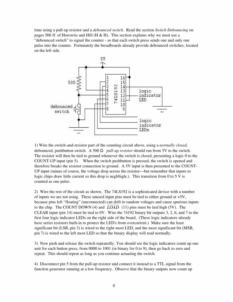
time using a pullup resistor and a debounced switch. Read the section Switch Debouncing onpages 506 ff. of Horowitz and Hill (H & H). This section explains why we must use a“debounced switch” to signal the counter so that each switch press sends one and only onepulse into the counter. Fortunately the breadboards already provide debounced switches, locatedon the left side.
1) Wire the switchandresistor part of the counting circuit above, using a normally closed,debounced, pushbutton switch. A 500 Ω pullup resistor should run from 5V to the switch.The resistor will then be tied to ground whenever the switch is closed, presenting a logic 0 to theCOUNTUP input (pin 5). When the switch pushbutton is pressed, the switch is opened andtherefore breaks the resistor connection to ground. A 5V input is then presented to the COUNTUP input (minus of course, the voltage drop across the resistor—but remember that inputs tologic chips draw little current so this drop is neglibigle.). This transition from 0 to 5 V iscounted as one pulse.
2) Wire the rest of the circuit as shown. The 74LS192 is a sophisticated device with a numberof inputs we are not using. These unused input pins must be tied to either ground or +5V,because pins left “floating” (unconnected) can drift to random voltages and cause spurious inputsto the chip. The COUNT DOWN (4) and LOAD (11) pins must be tied high (5V). TheCLEAR input (pin 14) must be tied to 0V. Wire the 74192 binary bit outputs 3, 2, 6, and 7 to thefirst four logic indicator LEDs on the right side of the board. (These logic indicators alreadyhave series resistors builtin to protect the LED's from overcurrent.) Make sure the leastsignificant bit (LSB, pin 3) is wired to the rightmost LED, and the most significant bit (MSB,pin 7) is wired to the left most LED so that the binary display will read normally.
3) Now push and release the switch repeatedly. You should see the logic indicators count up oneunit for each button press, from 0000 to 1001 (in binary for 0 to 9), then go back to zero andrepeat. This should repeat as long as you continue actuating the switch.
4) Disconnect pin 5 from the pullup resistor and connect it instead to a TTL signal from thefunction generator running at a low frequency. Observe that the binary outputs now count up
4

without your buttonpushing. Next, tie the CLEAR (pin 14) to a pullup resistor and a DIPswitch (see note below) and note its function. Lastly, tie the CARRY ( CO , pin 12) to a fifthlogic indicator LED and note its behavior. Keep this circuit together.
Note on DIP switch pullup setup:
Some people would call this a pulldown resistor since it connects to ground rather than 5V as inthe debounced switch setup above. To set this up use the row of DIP switches on the lower left ofthe prototyping board. The slideswitch on the far right internally connects one side of all theDIPs to either 0 or +5 V. Make sure this switch is set to 5V. To avoid shorting the 5 V supplydirectly to ground, a ~500Ω resistor to ground is needed. From the high side (5V) of thisresistor, run your input to the CLEAR pin (or where ever else in the circuit a manuallyoperatedlogic input is needed).2. Switching the input to 74LS192 On and Off with a NAND Gate
The voltmeter will work by counting the pulses from the 555 between the time the capacitorcharging starts, and the time the 355 comparator detects that the capacitor voltage has surpassedV
in and therefore changes its output state. To accomplish this we will use a simple NAND gate
in the circuit shown above. The NAND gate was discussed in class. A NAND is a NOT AND boolean circuit
element. The truth table is given in the diagram above. The pullup resistor will provide a logic1 to input A of the NAND when the switch is closed (this imitates the situation we will havewhile the capacitor is still charging), and 0 if the switch is open. Input B of the NAND isconnected to the pulse train output of the 555. The output of the NAND will therefore follow the555 pulse train (inverted) if the switch is closed, and the NAND output will just sit at logic 0otherwise. The signal from the pullup resistor and switch is said to gate the counting of the 555pulse train.
1) First explore the operation of the NAND. Find a 74LS00 IC and also its datasheet. The 7400actually has four independent NAND gates in one package. Just pick one of them for thisexercise. To drive the NAND, assemble the 555 timer circuit from page 287 of H & H. Youcould use the TTL generator, but the 555 will be needed later anyway. Select resistors and
5
capacitors to give a pulse repetition rate of a few Hz so that you can see the output changevisually. Then connect the 555 output pulse train to one input of the NAND, and the secondinput to the DIP switch with a pullup resistor.
2) Verify with a scope that the output of the NAND only oscillates when the DIP switch is closedand the input is therefore pulled up to +5 volts (logic 1)
3) Now wire the NAND output to the COUNT UP pin of the 74LS192 counter from thepreceding section. Verify that the counter only counts when the DIP switch is pulled up. If the555 pulse repetition rate is too high, you won't be able to see the four indicator LEDs switchingas the count progresses. They will look as if they are all on at the same time, with a reduction inbrightness. When the DIP switch is off though, the LED's should freeze in a steady pattern.
4) Use two probes and a scope to verify that the 555 signal is being inverted by the NAND. Youwill need to display both scope channels at once.
D. Improving the Analog Input/Transduction Section1. Constant Current Charging
Why is it unsatisfactory to charge the capacitor through a fixed resistor using a fixedvoltage? (Hint: V = V0(1exp(t/RC)). We now need a constant current capacitor chargingcircuit that can be turned on and off and reset to zero volts by the start and stop charging signals.This is a complex task, and thus part D will have several sub sections.
As explained at the very start of this writeup, the capacitor must be charged linearlywith time, so there is a fixed voltage rise per unit of time. How do we charge a capacitorlinearly? Recall that V = q / C and that 1 Amp = 1 Coulomb/ Sec. So, only if we charge thecapacitor with a constant current do we increment the charge by the same amount in eachsecond, hence also incrementing the voltage by a constant amount in each second. This gives alinear V(t). For the constant current drive we will use the LM334, a three terminal currentsource that just requires one external resistor to set the current.
An ideal current source would provide a fixed current no matter what load it wasconnected to. But, as with the voltage divider, any real current source will sag under certainconditions. Notice +VIN and V on the diagram below. The +VIN terminal is the power supplyvoltage input to the chip. The V terminal is the output pin from which the current (ISET) will besupplied to our load (the capacitor). As the signs indicate, V must be less than +VIN. If theloading is such that V gets too close to the supply voltage, the output current will sag or ceasealtogether. For correct operation we must satisfy the condition +VIN – V > 0.5V. Naturally thismeans we cannot charge our capacitor above (+VIN .5 V) . As with most IC's, there are manypossible applications and circuits for the 334. The figure below shows the simplestconfiguration. Vin can be anywhere between 1 and 40V. RSET determines the current by thefollowing formula: ISET = (227 V /K ) * Tambient / RSET. For this project, assume Tambient = 300K.In a real instrument, we would have to build in temperature compensation to make the chargingcurrent independent of the ambient temperature.
6

1) Using the above formula, calculate RSET to produce a current of 0.5mA.
2) Secure a copy of the datasheet for the LM334 so you can identify the leads. Assemble thelittle fragment shown above, powered by VIN =5 V, and measure the output current to verify yourcalculations. The 334 is temperature dependent, so warm it a little with your finger and see howthe current changes. It should be a small change. 3) Put the above constantcurrent source into the capacitor charging circuit of section B1, inplace of the 9K resistor to the positive supply as shown in the full circuit diagram on the lastpage of this writeup.
Verify the function of the circuit by placing an ammeter in series with the current sourceand capacitor, and watching the voltage on the capacitor with the oscilloscope. You shouldobserve on the scope that the capacitor never charges above (+VIN .5 V) = 4.5V as mentionedpreviously. The ammeter should show a .5mA reading until the capacitor voltage levels out near4.5 V, then it should read zero. Replace the 5V supply voltage with 10V. Notice that the currentis still the same. The 334 output current is independent of supply voltage. 4). Next, measure the slope of the capacitor charging curve V(t) on the oscilloscope and verify
that V(t) increases linearly with time. Compare the measured slope with the value you expectfrom calculation.
2. Automated Control of the Charging CircuitGiven the measured current of your 334, calculate a capacitor value to give a charging
rate in Volts / second between 100 and 200 V / s. This choice will allow the final meter circuitto reread the input voltage at a fairly high repetition rate, allowing it to follow if the inputvoltage varies with time. For example, if I = 0.5 mA and C = 3.3 x 10⁶ F, V(t) = .5mC / s / 3.3 x10⁶ F = 150 V / s. This implies .006 seconds per volt.
To start and stop the capacitor charging circuit automatically, we will use a device calleda MOSFET transistor as an electronic switch. The MOSFET to be used here is called anRFP4N05L. MOSFETs are extremely sensitive devices meaning they are easy to destroy bystatic electricity. Ground yourself to the shell of a BNC connector on the breadboard beforehandling the MOSFET. The terminals of this device are named gate, source, and drain. Thegate is the control terminal which controls how much current passes from drain to source. Muchof the magic of MOSFETs is related to the fact that the gate draws an exceedingly small current,picoamps or less. With that tiny current (and correspondingly tiny control power IgateVgate) wecan control a much larger current Idrain of hundreds of mA (and correspondingly much larger
7

power Idrain *(VdrainVsource)) going from drain to source. These devices come in a variety of
types with different characteristics, but we do not need to concern ourselves with that now.
We will build up the automated control of the charging circuit in steps.1) First let's see how to use the MOSFET to start and stop the charging. The device will actessentially like a switch across the capacitor that we can open and close but it will open andclose in response to a logic signal presented to its gate. Rearrange your capacitor circuit frompart B once again, this time to look like the figure above (the 0.5mA comes from the 334 currentsource as before). Supply a variable Vin (as before) using a 1k potentiometer between ground and10 V. Measure Vin with a knownworking voltmeter. Notice we are tying the gate of the MOSFET to a DIP switch and pullup resistor. We are still going to operate a manual switch to startand stop the charging, but now the manual switch is actually just presenting a logic signal to theMOSFET gate. That signal causes the MOSFET “switch” to open and close. Later on, thelogic signal will be supplied by yet another chip (the 74LS74 flipflop) instead of a manualswitch.
2) Verify that when the DIP switch at the MOSFET gate is opened and closed, the LEDs toggleas before. When the gate is taken low, the MOSFET acts like an open circuit from drain tosource, allowing the capacitor to charge. When the gate is taken high, the MOSFET acts like aclosed switch shorting across the capacitor and bringing the charge to zero. Observe that theMOSFET gets warm to the touch. It is passing current (~.5mA) whenever the gate is high.
3) Though charging linearly, the capacitor charges too fast to visually see the delay between redand green LED's caused by the charging time. To verify the delay, attach the probe of anoscilloscope across the capacitor and watch it charge and discharge for several different valuesof Vin. It may be difficult to get the scope to trigger properly (you should be on normaltriggering), but persevere! Verify that the slope, etc. are still the same as they were in D1 step 5)above.B. Controlling the MOSFET with a 74LS74 FlipFlop
The 74LS74 is a clocked Dtype flipflop. We will use it to mediate between thecomparator and the capacitor charging circuit. This device has power and ground connectionslike any logic IC. It also has inputs called D, CLOCK, and R Rbar and outputs called Q andQ . The presence of a CLOCK pulse determines whether or not the device “listens” to the D
input. Without a logic 1 signal at CLOCK, the outputs stay constant no matter what happens atD. If both CLOCK and D are driven with logic 1 at the same time, then Q will go to logic 1 andQ will go to logic 0. If CLOCK is driven with logic 1 and D is driven with logic 0 at the same
time, then Q will go to logic 0 and Q will go to logic 1. If R is driven with logic 0 it willforce Q to logic 0 and Q to logic 1 regardless of the logic level presented to CLOCK.
8

Wire up a 74LS74 and connect the R input to 5 V. Using pullup resistors and DIPswitches connected to D and CLOCK, and logic indicator LED's connected to Q and Q , verifythat the above description of its operation is correct.
Next explore the effect of R . Connect D to +5 V so that it is always high (logic 1), andRbar to a switch and pull up resistor. What should happen when Rbar input is grounded?(Hint remember the Triggerbar input on a 555?). Verify that the effect of Rbar is to “jam” Qto zero regardless of the signal presented to CLOCK.
In the final DVM circuit, the comparator will drive R and CLOCK will be driven by a pushbutton, or by the TTL pulse train from the function generator. The D input will be tied to+5 V. How these connections perform the necessary measurement cycle will be explained in thenext section.
Part D.3Now we will put together the parts discussed so far and get the automated charging
operation cycle to work. We will then add one refinement, and then move on to the latching anddisplay section of the DVM circuit.
1) Once again amend your capacitor charging circuit, making it look like that above. Thedebounced switch connects to the 74LS74 CLOCK input and is wired as in part C.1 step one.The switch is there to allow us to manually generate a logic signal to start one charging cycle justfor testing. This logic signal could alternatively be generated automatically.
2) Run Q to an indicator LED. Also, run Q to an indicator, as well as to the MOSFET gate(determine which MOSFET pin is which from a data sheet). Tie R to a third indicator LED,as well as to the opamp (comparator) output. As ever, the 355 opamp takes as its inputs thevoltage we wish to measure and the voltage of the charging capacitor. Whenever Vin > VCap thecomparator output is +10V. In the other case, VCap > Vin, the output is –10V (the power supplyvoltages +/10 V are often referred to as the rails). The opamp output controls the operation ofthe D flipflop (through R ).
So, lets go through a cycle of operation. Assume that initially (at powerup) thecapacitor is uncharged. Therefore Vin > VCap, R = 1, Q = 0, and Q = 1. The Q =1 signalpulls the RFP4N05L gate high, so the MOSFET “switch” is closed, shorting across thecapacitor.
Now we press the debounced switch and send a signal to the CLOCK input of the74LS74. That chip then reads the signal at its D input, which is always logic 1 (D is tied to+5V). Therefore the 74LS74 output state changes to Q = 1 and Q = 0. Q = 0 immediately
9

opens the MOSFET switch, allowing the capacitor to start charging. Later we will use the Qoutput to start the counting and display sections (not shown in the diagram above).
The capacitor continues to charge until VCap > Vin. As soon as VCap exceeds Vin, theoutput of the opamp comparator goes low, driving the R input to logic 0. This resets the flipflop to the state Q = 0 and Q = 1, which closes the MOSFET “switch” again and instantlydrains the capacitor. The state of the circuit is now exactly the same as it was at powerup.Nothing more will happen unless another logic 1 is presented to CLOCK.
The outcome of all this is that every time the debounced switch is pressed, the capacitorgoes through one cycle of charging at .5 mA up to VCap = Vin, then gets instantly discharged. TheQ signal of the 74LS74 is logic 1 during the charging time and logic 0 otherwise. This switchingof Q and Q in time with the capacitor charging is the heart of the DVM we are building. Wewill use this to control the counting and display circuitry in the following sections.
3) Power the above circuit and use indicator LED's or an oscilloscope to check that it actuallygoes through the cycle explained in detail above. Basically, you should see Q = O and Q = 1 atpowerup. Then pressing the switch should reverse the states of Q and Q for a short time, afterwhich they should return to their initial states. It will be very difficult to see R switch from itspowerup value of 1, to 0, and back to 1 again, since it is only in the logic 0 state for thatincredibly brief period of time it takes the capacitor to start discharging. 4) At the beginning of this section, the need for a couple of refinements was mentioned. Here isthe symptom of a need for one of them: Notice that if you hold down the switch, the capacitorwill charge up, but it will not discharge until you let go.
Part D.4: A RefinementWhy does the capacitor not discharge if the switch is held down? The poor 74LS74 is
getting contradictory messages from its inputs, that's why. As long as the switch is pressed, the74LS74 is sensitive to its D input, which is held high. So this should make the output state go toQ = 1 and Q = 0. However once the capacitor gets fully charged, the opamp comparator outputis signaling R = 0, which is supposed to drive the outputs to Q = 0 and Q = 1 instead.According to the 74LS74 specs, the D input “wins” this conflict and the capacitor never getsdischarged.
There are two ways to fix this. 1) Use an edge triggered 74LS74, which does exist and iscalled a 74LS74A. We discussed edge triggered logic devices in class. Or, 2) send only a veryshort pulse to the CLOCK input no matter how long the switch is held down. The circuit shownbelow accomplishes fix number 2) in a “crude but effective” way.
You should have learned about NOT, NOR, and NAND in lecture. In Boolean logic theyperform their functions instantaneously, but in the realm of electronics there is some propagation
10

delay. For example, the inverting of a signal (NOT) may take around 20ns. So here is the deal:with the debounced switch open, the upper input to the NOR is 1. The lower input, produced bythe three NOTs, is 0. Recall that a NOR only outputs a 1 when both inputs are 0, so here itoutputs 0. Now we close the switch. The upper input to the NOR immediately goes to 0. Due tothe propagation delay through the three NOTs, the lower input stays at 0 also, for about 60ns ofpropagation delay. Then it turns to 1. The effect of this is that the NOR output gives a 60nspulse of 1, then returns to 0. When we release the switch (long after the 60 ns pulse is finished),the upper input immediately goes back to 1, and 60ns later the lower input goes to 0. But noneof this changes the output, since at any time one of the inputs is 1. A circuit that generates ashort pulse like this is called a “one shot”. Single IC’s that perform this function are actuallyavailable and are discussed in H & H p. 517 ff.
1) Add in the NOR and three NOTs between the switch and flipflop. The NOR is a 74LS04and the NOT is a 74LS02. You, of course, need the data sheet for these parts. Do not forget togive them 5V and ground! Observe on the scope that the capacitor will now discharge even ifyou hold down the switch.
Part E: Latch and Display SectionHere we need to create a human readable display of our pulse counting. This will
involve a seven segment display, a display driver, and a latch.1. Display and Driver
The MAN71A is a sevensegment LED display used for displaying a single humanreadable number or other character. It contains seven barshaped LED's arranged in the shape ofa squaredoff “8”. The “anode” (+ terminal in forward bias) connections of all the LED's aremassed together into a single “common anode” terminal. The cathode of each segment has itsown wire coming out of the DIP package. The segments are designated with letters a – g. Tolight any one or more of the segments simply ground the corresponding pin(s) on the DIP.
To display a given digit one has to take the desired digit and “decode” it into a list ofwhich pins are to be grounded. The IC chip 7447 contains all the circuitry needed to do thisdecoding. As its input it receives the (four) binary digits of a number between 0 and 9, and“decodes” this information into which LED segments should light, grounding the correspondingpins of its output.
Look up the datasheets for the 7447 and MAN71A. Note that the MAN71A LED's arenot internally overcurrentprotected, so a 500Ω resistor is required on each segment's line toground, meaning between the MAN71A and the 7447. [Why wouldn't it be a good idea to putone such resistor in the common anode line?] 2. Latch
The latch allows us to statically display the final result of one capacitor charging cycleoperation, even while the next cycle is in progress.
The latch we use here, the 74LS175, has four inputs and four outputs. It just passesalong the logic states on its inputs through to its outputs but only when an ENABLE signal isdriven to logic 1. Each time an ENABLE=1 signal is received, the 74LS175 transfers its inputdata to its outputs, whereupon it freezes the outputs until another ENABLE signal arrives.
Obtain the datasheet for the 74LS175. You will see that fortunately for us, the ENABLE(also sometimes called CLOCK) input is positive edge triggered, meaning the chip only passesthe input bits to the outputs on the CLOCK transition from 0 to 5V. No worries about multiplepassalongs from one overlong CLOCK pulse, and no need for a homemade oneshot like with
11

the 74LS74. The freezetheoutputstillthenextCLOCKpulse action is just what we need forour static display.
1) In the circuit from part B, connect the four output bits from the counter to the inputs of thelatch. (You can leave the indicator LEDs connected too if you wish).2) Run the output of the 74LS175 to the the 74LS47 decoder for the MAN71A. Make sure toconnect the LSB output of the counter to the LSB input of the decoder, and not LSB to MSB orsomething else.3) Connect the COUNT UP pin of the counter to the TTL ouput of the function generator and setthe repetition rate for about 1 Hz using your oscilloscope. Set up a debounced switch with pullup resistor so that actuating the switch presents a logic 1 signal to the CLOCK input of the74LS175 latch.4) Verify operation of the circuit: No number should appear on the display until you hit theswitch, “enabling” the latch. No matter that the function generator is running, no change on thedisplay should then occur until you actuate the switch again. Press the switch twice insuccession 5 or 10 seconds apart and verify that the change in the number displayed agrees withwhat you expect from the TTL pulse rate and the time interval between buttonpresses. To avoidhaving to subtract the starting and ending values, you could present a logic 1 signal to theCLEAR input of the 74LS192 counter after each count, using yet another switchandpullup.The display will of course have to be cleared like this in the final circuit after each chargingcycle is counted and displayed.
Part F: Completing the DVMTo complete the DVM we finally connect the analog input/transduction section , the
clock generator, the counting section, and the latchanddisplay section. See the markedupdrawing at the end of this writeup. 1) Reconnect a debounced switch as the input to the oneshot going to the 74LS74 CLOCKinput.2) Remove all the other manual switchandpullup setups from the circuits. Connect the Qoutput from the 74LS74 and also the 555 timer output to the two inputs of the NAND. This willpass along the 555 pulse train only during the capacitor charging phase. 3) Connect the output of the NAND to the COUNT UP of the 74LS192 counter. The counterwill count the pulses that come during the capacitor charging phase.4) Connect the Q output of the 74LS74 to the ENABLE (or CLOCK) pin of the 74LS175latch. This will cause the result of the count to be latched into the output bits of the 74LS175when Q goes high at the conclusion of each capacitor charging phase.5) In addition to latching the count, it is also necessary to clear the counter each cycle. Thiscould be done simply by connecting the 74LS74 Q output to the CLEAR pin of the 74LS192counter. But this would not quite work, because Q is also doing the latching. We couldn't besure that the data was latched and displayed before the counter was cleared and the informationlost. This type of timing condition is called a logic race. It is simple to avoid connect the Qto CLEAR after running it through two 74LS02 inverters (NOT gates) to delay it by about 20 ns.6) At last, make a final check with the oscilloscope: connect the capacitor voltage to onechannel on the scope, and the pulse train from the NAND to the second channel. Set VIN to say3 volts with the pot and then start a measuring cycle using the debounced switch on the 74LS74CLOCK input. Visually count the number of pulses you see during the capacitor charging time.Vary VIN and get an idea of the number of pulses per volt of VIN (if you followed instructions,
12

it should be around 1). 7) Let her run! Take several readings each for several values of VIN . Make a table of VIN vs.displayed counts. Demonstrate that the relationship is linear (there will be some error due to thecounting uncertainty of 1 puls e and the slow pulse rate chosen for a 1digit display.).Demonstrate that the measurements are repeatable (measure, say 1V, then 8V, then 1V again andsee if you get the result same as the first time). If any of these things are false, explain why(maybe a circuit element has heated due to dissipative power and change operatingcharacteristics?).Part Final+ extended lab (optional)
Only having a one digit display is a bit of a drawback, especially since we see somevariation in this digit. You can easily expand it to be a two digit display by sending the CARRYoutput of the 74LS192 counter to a second identical latching and display section . Also, withtwo digits you can count 100 pulses during the charging time rather than only 10 with a singledigit. Therefore the clock rate generated by the 555 should be increased by a factor of roughlyten. If you do this part, make another graph of VIN vs. counts to check the range and linearity,and verify the reproducibility.
13

Full circuit with sections outlined and named.
14

15