Embed Size (px)
Citation preview
Digital VLSI ADigital VLSI ADigital VLSI ADigital VLSI A
Pipelining & ParaPipelining & Para
Mahdi S
fSharif University
© M. Shabany, Digital
Architectures:Architectures:Architectures:Architectures:
allel Processingallel Processing
Shabany
fy of Technology
l VLSI Architectures
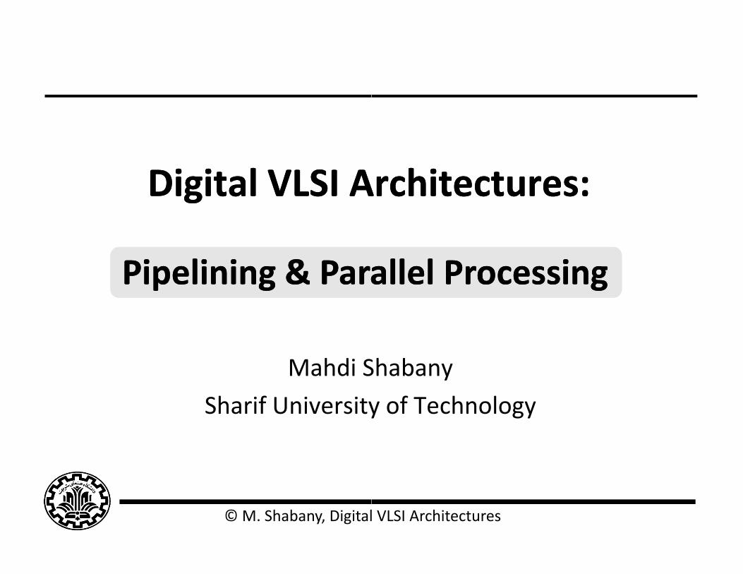
Architectural Techniques : Critical path in any design is the longe
1. Any two internal latches/flip‐flops
2. An input pad and an internal latch2. An input pad and an internal latch
3. An internal latch and an output pad
4. An input pad and an output pad
Use FFs right after/before
input/out pads to avoid
th l t th
InputPad
the last three cases
(off‐chip and packaging delay)
The maximum delay between anyThe maximum delay between anytwo sequential elements in a design will determine the max
clock speed
© M. Shabany, Digital
: Critical Pathest path between
d
Comb. Logic
2
31OutputPad
4
l VLSI Architectures
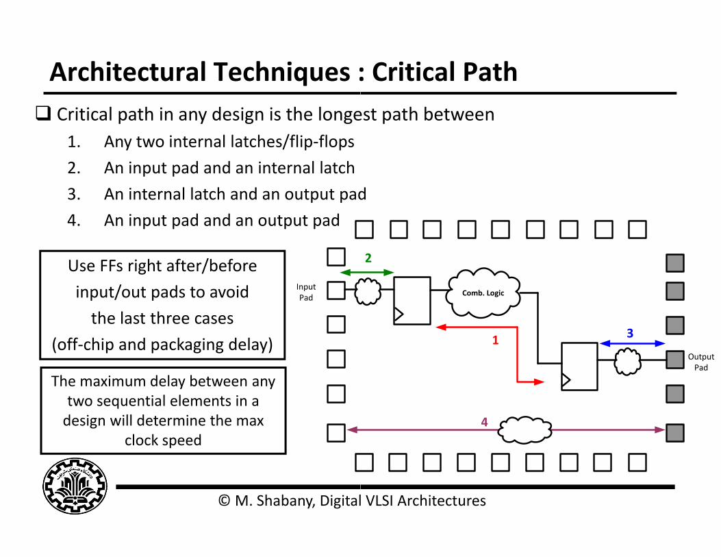
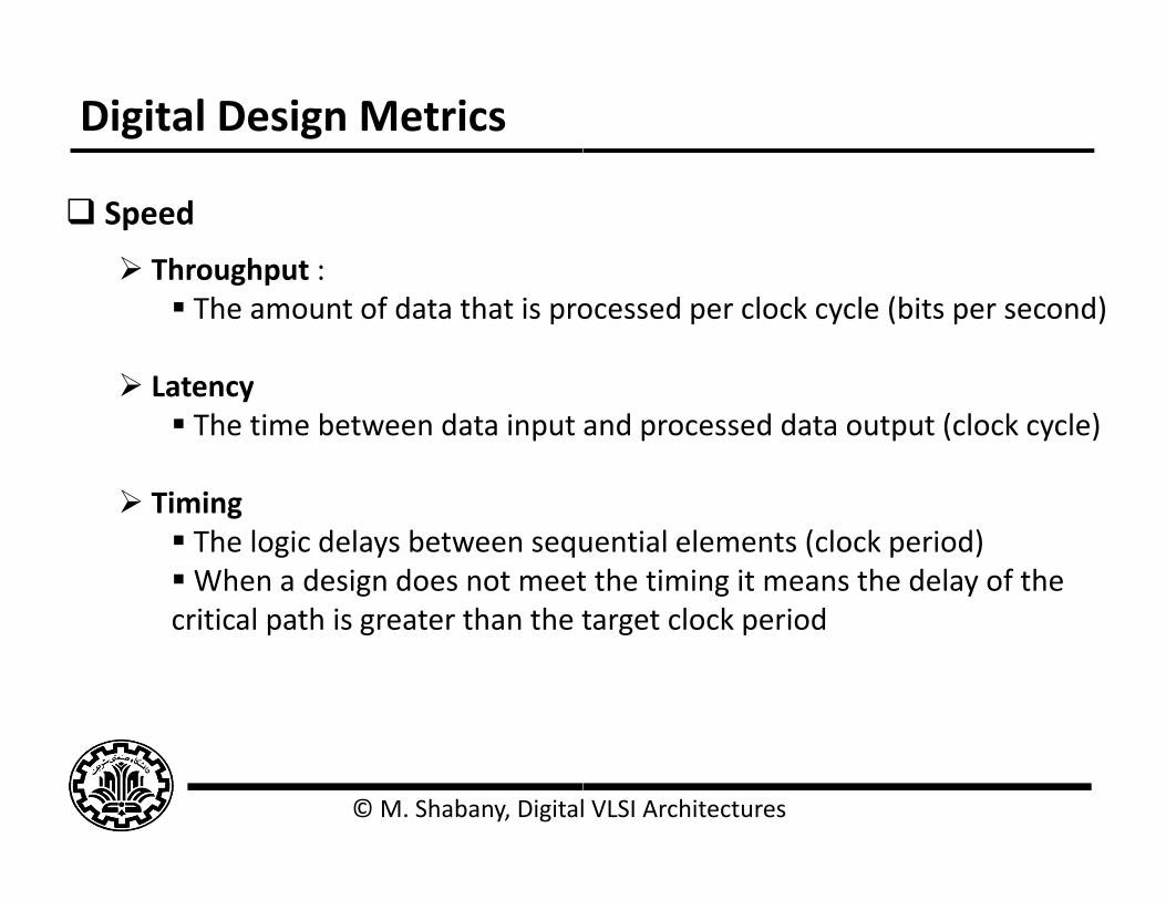
Digital Design Metrics
Three primary physical character
Speed Speed Throughput Latency Timing Timing
Area Power
© M. Shabany, Digital
istics of a digital design:
l VLSI Architectures
Digital Design Metrics
Speed
Throughput :oug put The amount of data that is pro
Latency Latency The time between data input
Timing Timing The logic delays between sequWhen a design does not meetcritical path is greater than the tcritical path is greater than the t
© M. Shabany, Digital
ocessed per clock cycle (bits per second)
and processed data output (clock cycle)
uential elements (clock period)t the timing it means the delay of the target clock periodtarget clock period
l VLSI Architectures
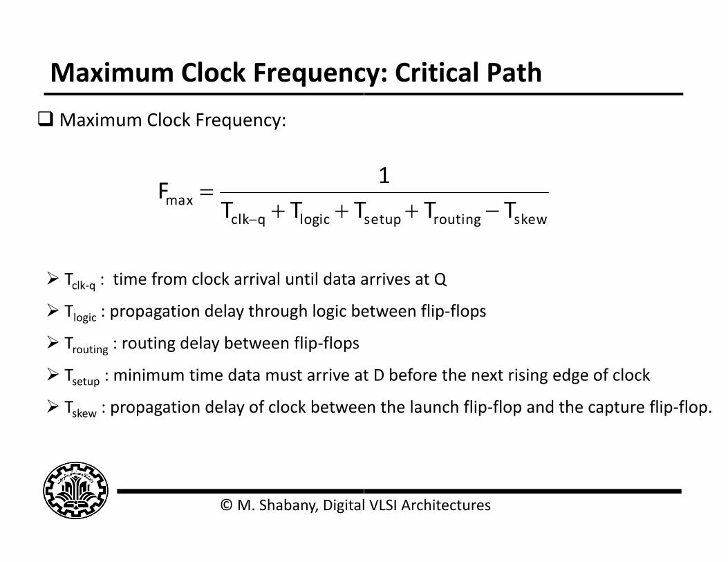
Maximum Clock Frequenc
Maximum Clock Frequency:
logicqclkmax TTTF
Tclk‐q : time from clock arrival until data a
Tlogic : propagation delay through logic be Tlogic : propagation delay through logic be
Trouting : routing delay between flip‐flops
Tsetup : minimum time data must arrive at
Tskew : propagation delay of clock betwee
© M. Shabany, Digital
cy: Critical Path
1
skewroutingsetup TTT1
arrives at Q
etween flip‐flopsetween flip flops
t D before the next rising edge of clock
en the launch flip‐flop and the capture flip‐flop.
l VLSI Architectures
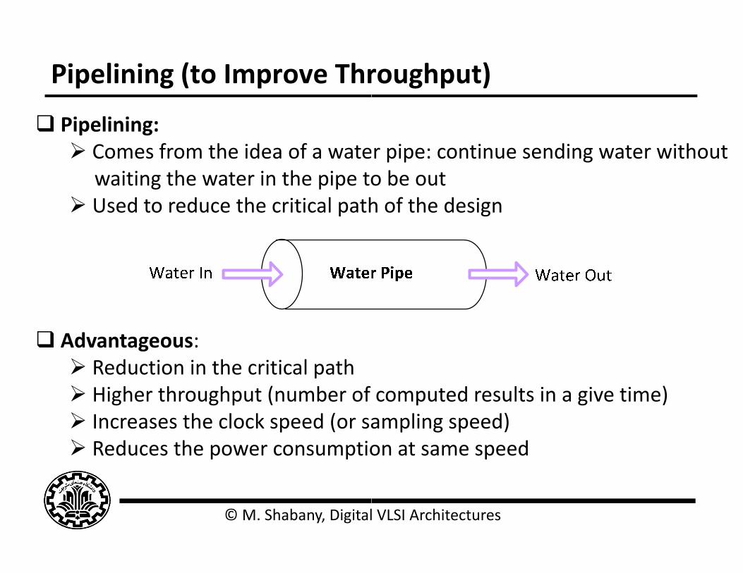
Pipelining (to Improve Thr
Pipelining: Comes from the idea of a wate
waiting the water in the pipe towaiting the water in the pipe to Used to reduce the critical path
Advantageous: Reduction in the critical path Higher throughput (number of Higher throughput (number of Increases the clock speed (or sa Reduces the power consumptio
© M. Shabany, Digital
roughput)
r pipe: continue sending water withouto be outo be outh of the design
computed results in a give time)computed results in a give time)ampling speed)on at same speed
l VLSI Architectures

Architectural Techniques :
Pipelining:
Very similar to the assembly line i
The beauty of a pipelined design ibefore the prior data has finished, massembly line.
© M. Shabany, Digital
:Pipelining
n the auto industry
s that new data can begin processing much like cars are processed on an
l VLSI Architectures
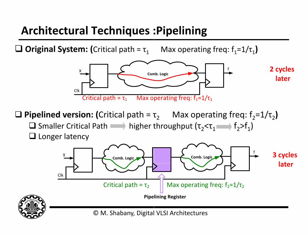
Architectural Techniques : Original System: (Critical path = τ1
ComX
Com
Clk
Critical path = τ1 Max o
Pipelined version: (Critical path = τ Smaller Critical Path higher t l Longer latency
Comb. LogicX
Clk
Critical path = τ2
© M. Shabany, Digital
Pipe
:PipeliningMax operating freq: f1=1/τ1)
2 cycles mb Logic
f
latermb. Logic
perating freq: f1=1/τ1
τ2 Max operating freq: f2=1/τ2)throughput (τ2<τ1 f2>f1)
3 cycles later
Comb. Logicf
later
Max operating freq: f2=1/τ2
l VLSI Architectures
lining Register
Architectural Techniques :
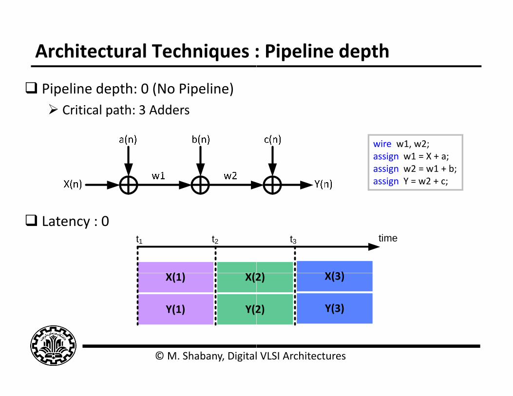
Pipeline depth: 0 (No Pipeline) Critical path: 3 Adders
Latency : 0 Latency : 0
( ) (
t1 t2
X(1)
Y(1)
X(2
Y(2
© M. Shabany, Digital
: Pipeline depth
wire w1, w2;assign w1 = X + a;assign w2 = w1 + b;g ;assign Y = w2 + c;
)
timet3
X(3)2)
2)
X(3)
Y(3)
l VLSI Architectures
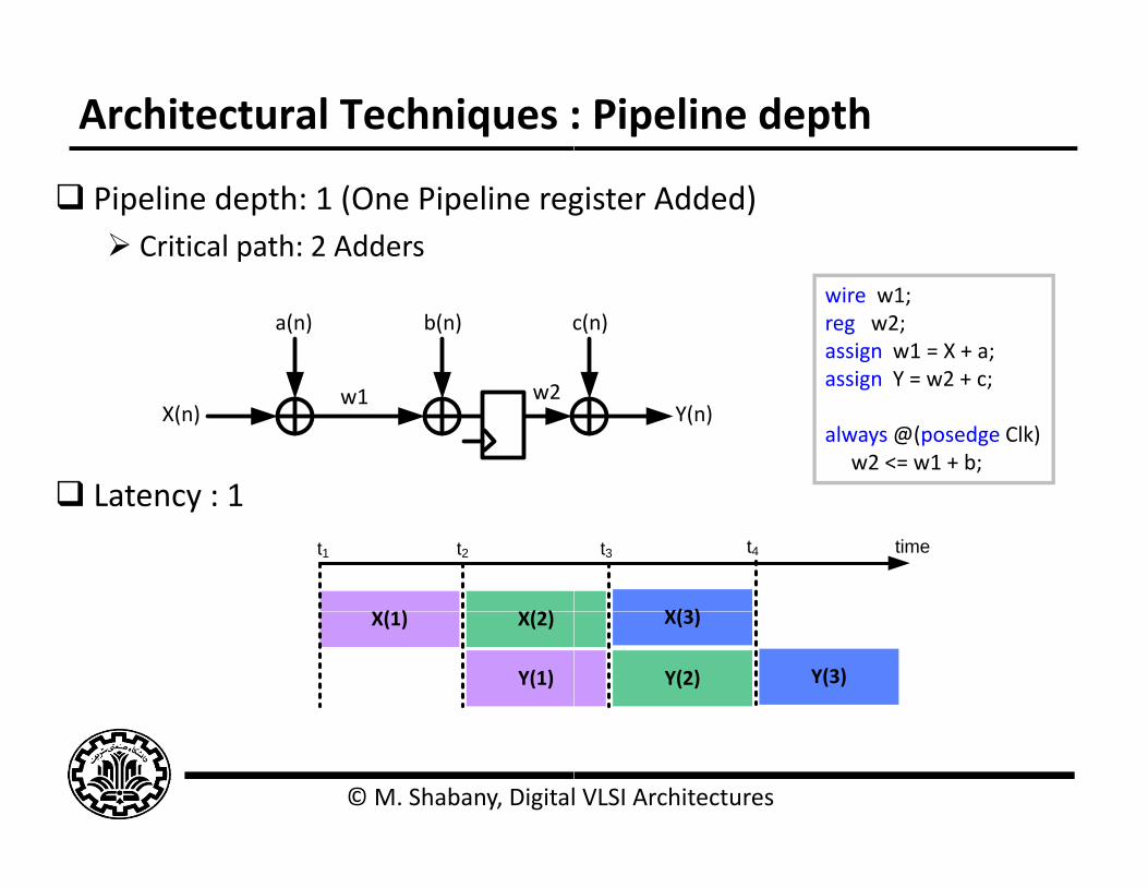
Architectural Techniques :
Pipeline depth: 1 (One Pipeline reg Critical path: 2 Adders
a(n) b(n) c
2
Latency : 1
X(n)w1 w2
Latency : 1
( ) (2)
t1 t2
X(1)
Y(1)
X(2)
© M. Shabany, Digital
: Pipeline depth
gister Added)
wire w1;reg w2;assign w1 = X + a;assign Y = w2 + c;
c(n)
g ;
always @(posedge Clk)w2 <= w1 + b;
Y(n)
timet3
X(3)
t4
Y(2)
X(3)
Y(3)
l VLSI Architectures
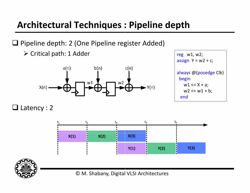
Architectural Techniques :
Pipeline depth: 2 (One Pipeline reg Critical path: 1 Adder
Latency : 2 Latency : 2
t1 t2 t3
X(1) X(2)
© M. Shabany, Digital
: Pipeline depth
gister Added)reg w1, w2;assign Y = w2 + c;assign Y = w2 + c;
always @(posedge Clk)beginw1 <= X + a;w1 <= X + a;w2 <= w1 + b;
end
t4 t5
Y(1) Y(2)
X(3)
Y(3)
l VLSI Architectures
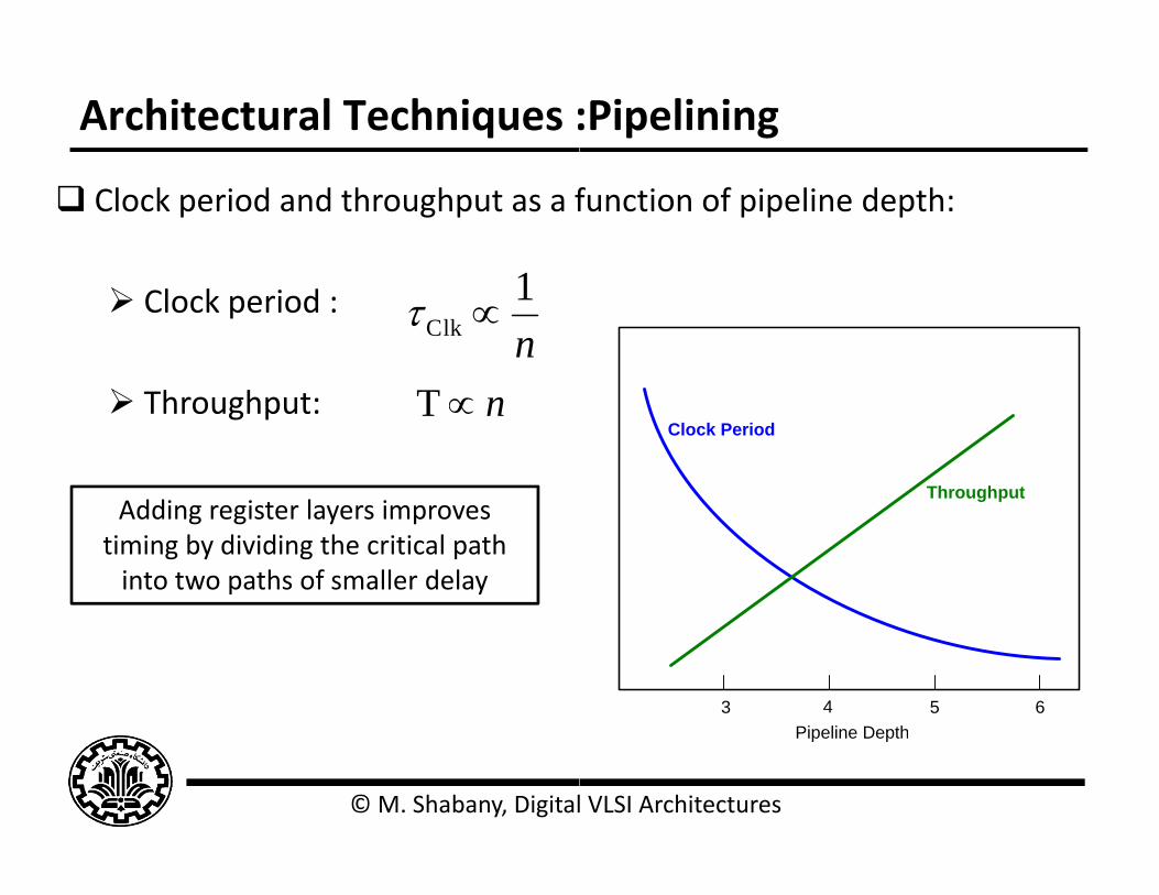
Architectural Techniques :
Clock period and throughput as a f
1 Clock period :
h h Tn1
Clk
Throughput: nT
Addi i t l iAdding register layers improves timing by dividing the critical path into two paths of smaller delay
© M. Shabany, Digital
:Pipelining
function of pipeline depth:
Clock Period
Throughput
3 4 5 6Pipeline Depth
l VLSI Architectures
Pipeline Depth
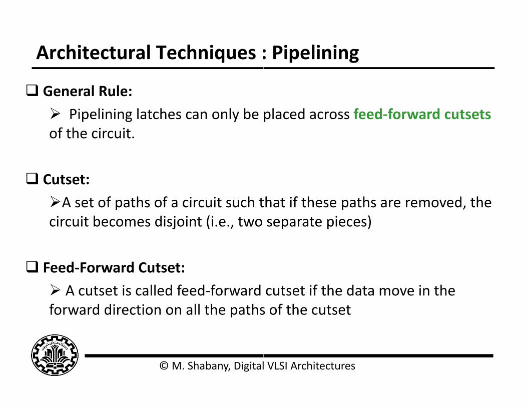
Architectural Techniques :
General Rule:
Pipelining latches can only be of the circuit.
Cutset: Cutset:
A set of paths of a circuit such tcircuit becomes disjoint (i.e., two j
Feed‐Forward Cutset:
A cutset is called feed‐forward forward direction on all the paths
© M. Shabany, Digital
: Pipelining
placed across feed‐forward cutsets
that if these paths are removed, the separate pieces)p p
cutset if the data move in the s of the cutset
l VLSI Architectures
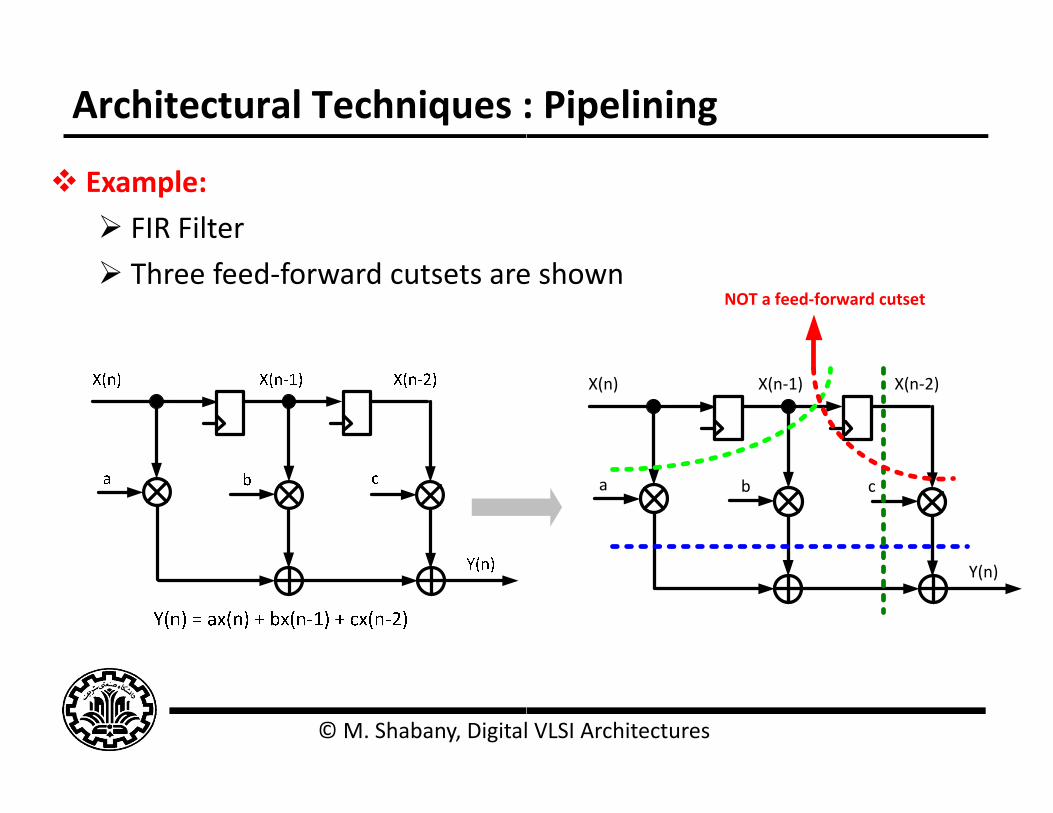
Architectural Techniques :
Example:
FIR Filter
Three feed‐forward cutsets are
© M. Shabany, Digital
: Pipelining
e shownNOT a feed‐forward cutset
X(n) X(n‐1) X(n‐2)
a b c
Y(n)
l VLSI Architectures
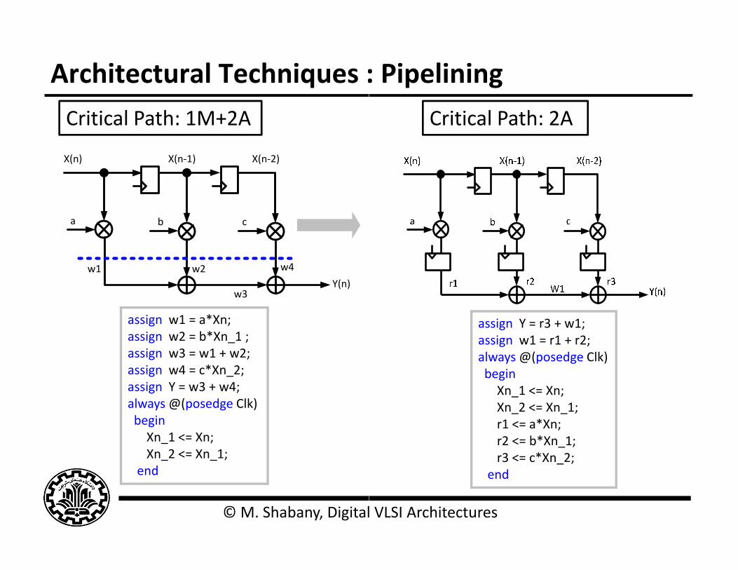
Architectural Techniques :Critical Path: 1M+2A
X(n) X(n‐1) X(n‐2)
a b c
assign w1 = a*Xn;
Y(n)w1 w2
w3
w4
assign w1 = a Xn;assign w2 = b*Xn_1 ;assign w3 = w1 + w2;assign w4 = c*Xn_2;assign Y = w3 + w4;g ;always @(posedge Clk)beginXn_1 <= Xn;Xn_2 <= Xn_1;
© M. Shabany, Digital
end
: PipeliningCritical Path: 2A
assign Y r3 + 1assign Y = r3 + w1;assign w1 = r1 + r2;always @(posedge Clk)beginXn 1 <= Xn;Xn_1 < Xn;Xn_2 <= Xn_1;r1 <= a*Xn; r2 <= b*Xn_1;r3 <= c*Xn_2;
l VLSI Architectures
end
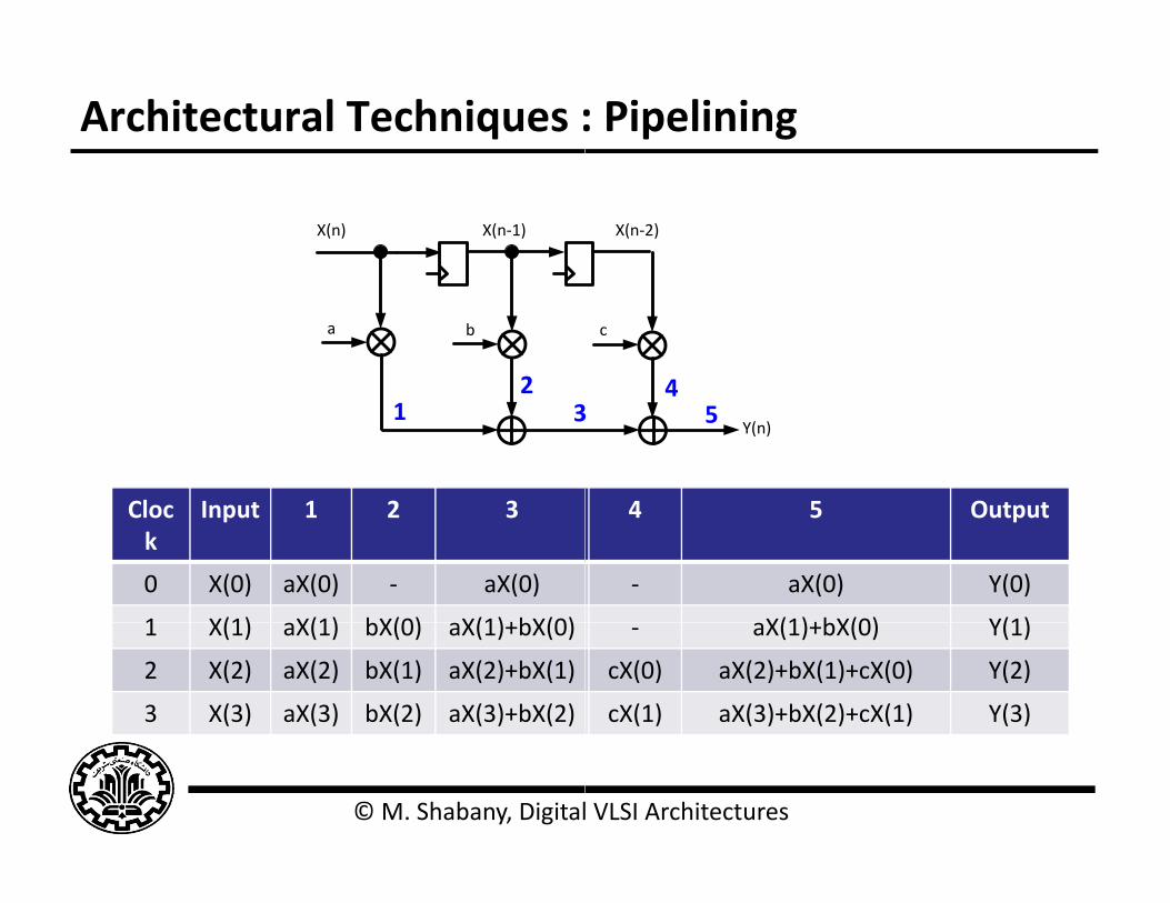
Architectural Techniques :
X(n) X(n‐1)
a b
2
Cloc Input 1 2 3
1 3
Clock
Input 1 2 3
0 X(0) aX(0) ‐ aX(0)
1 X(1) X(1) bX(0) X(1)+bX(0)1 X(1) aX(1) bX(0) aX(1)+bX(0)
2 X(2) aX(2) bX(1) aX(2)+bX(1)
3 X(3) aX(3) bX(2) aX(3)+bX(2)
© M. Shabany, Digital
: Pipelining
X(n‐2)
c
4
4 5 Output
Y(n)3
45
4 5 Output
‐ aX(0) Y(0)
X(1)+bX(0) Y(1)‐ aX(1)+bX(0) Y(1)
cX(0) aX(2)+bX(1)+cX(0) Y(2)
cX(1) aX(3)+bX(2)+cX(1) Y(3)
l VLSI Architectures

Architectural Techniques :X(n) X(n‐1)
a b
1 2
Cloc Input 1 2 3
1
Clock
Input 1 2 3
0 X(0) ‐ ‐ ‐
1 X(1) aX(0) ‐ aX(0)1 X(1) aX(0) ‐ aX(0)
2 X(2) aX(1) bX(0) aX(1)+bX(0)
3 X(3) aX(2) bX(1) aX(2)+bX(1)
© M. Shabany, Digital
: PipeliningX(n‐2)
c
2 3 4 5
4 5 Output
Y(n)3 5
4 5 Output
‐ ‐ ‐
‐ aX(0) Y(0)‐ aX(0) Y(0)
) ‐ aX(1)+bX(0) Y(1)
) cX(0) aX(2)+bX(1)+cX(0) Y(2)
l VLSI Architectures

Architectural Techniques :
Even more pipelining
Clock Input 1 2 3
0 X(0) ‐ ‐ ‐
1 X(1) aX(0) ‐ -2 X(2) aX(1) bX(0) aX(0)
3 X(3) aX(2) bX(1) aX(1)+bX(0)
4 X(3) aX(2) bX(1) aX(2)+bX(1)
© M. Shabany, Digital
: Pipelining
4 5 Output
‐ ‐ ‐
‐ - -‐ aX(0) Y(0)
‐ aX(1)+bX(0) Y(1)
cX(0) aX(2)+bX(1)+cX(0) Y(2)
l VLSI Architectures

Architectural Techniques :
Pipelining at the operation level
Break the multiplier into two p
Fine‐PiPipe
© M. Shabany, Digital
: Fine‐Grain Pipelining
arts
X(n) X(n‐1) X(n‐2)
a b cm1 m1 m1
‐Grainli i
m2 m2 m2
lining
Y(n)
l VLSI Architectures

Unrolling the Loop Using P
Calculation of X3Throughput = 8/3, or 2.7 bits/clockLatency = 3 clocksLatency 3 clocksTiming = One multiplier in the critical
Iterative implementation:p No new computations can begin un
previous computation has complet
© M. Shabany, Digital
Pipelining
module power3(output reg [7:0] X3,output finished,
path input [7:0] X,input clk, start); reg [7:0] ncount;reg [7:0] Xpower, Xin;
ntil theted
assign finished = (ncount == 0);always@(posedge clk)if (start) beginXPower <= X; Xin<=X;ncount <= 2;X3 <= XPower;endelse if(!finished) beginncount <= ncount ‐ 1;XPower <= XPower * Xin;End
endmodule
l VLSI Architectures
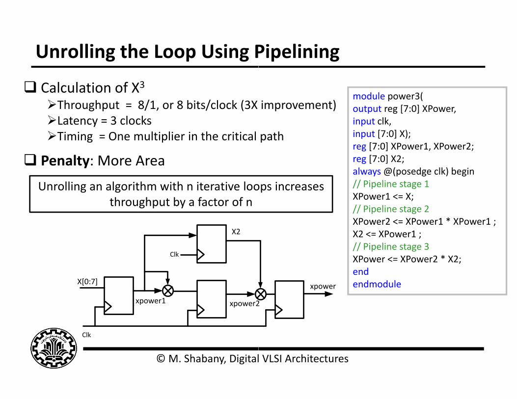
Unrolling the Loop Using P
Calculation of X3Throughput = 8/1, or 8 bits/clock (3X Latency = 3 clocksLatency 3 clocksTiming = One multiplier in the critical
Penalty: More Area
Unrolling an algorithm with n iterative loothroughput by a factor of n
Clk
X2
X[0:7]
xpower1 xpower2
© M. Shabany, Digital
Clk
Pipelining
improvement)module power3(output reg [7:0] XPower,input clk,
pathinput clk,input [7:0] X);reg [7:0] XPower1, XPower2;reg [7:0] X2;always @(posedge clk) beginalways @(posedge clk) begin// Pipeline stage 1XPower1 <= X;// Pipeline stage 2XPower2 <= XPower1 * XPower1 ;
ops increases
;X2 <= XPower1 ;// Pipeline stage 3XPower <= XPower2 * X2;endendmodulexpower
2
l VLSI Architectures
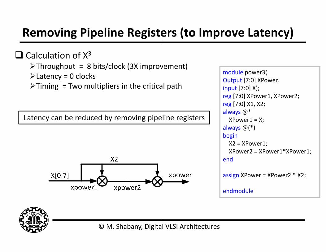
Removing Pipeline Registe
Calculation of X3Throughput = 8 bits/clock (3X improvLatency = 0 clocksLatency 0 clocksTiming = Two multipliers in the critica
Latency can be reduced by removing pipel
© M. Shabany, Digital
ers (to Improve Latency)
vement)module power3(O t t [7 0] XP
l pathOutput [7:0] XPower,input [7:0] X);reg [7:0] XPower1, XPower2;reg [7:0] X1, X2;l @*always @* XPower1 = X;
always @(*)beginX2 XP 1
line registers
X2 = XPower1;XPower2 = XPower1*XPower1;
end
i XP XP 2 * X2assign XPower = XPower2 * X2;
endmodule
l VLSI Architectures
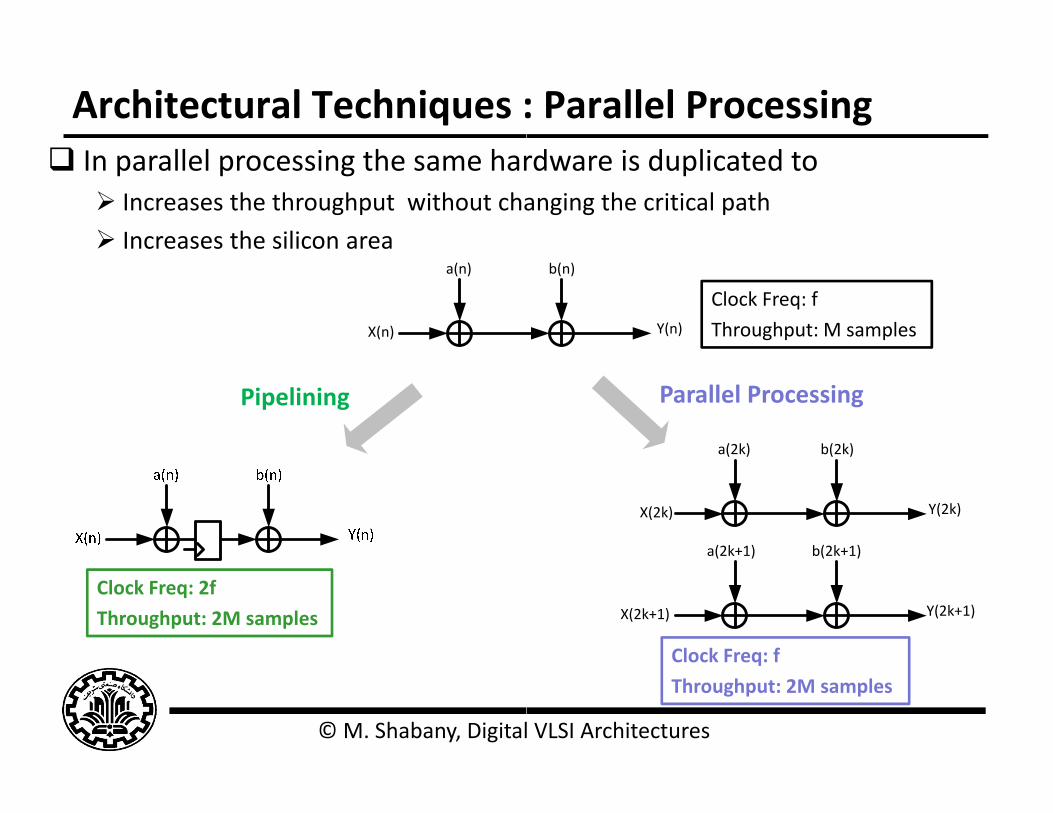
Architectural Techniques : I ll l i h h In parallel processing the same har
Increases the throughput without cha
Increases the silicon area
X(n)
a(n)
Pipelining
Clock Freq: 2f
Throughput: 2M samples
© M. Shabany, Digital
: Parallel Processingd i d li drdware is duplicated toanging the critical path
b(n)
Y(n)
Clock Freq: f
Throughput: M samples
a(2k) b(2k)
Parallel Processing
X(2k) Y(2k)
a(2k+1) b(2k+1)
X(2k+1) Y(2k+1)
Clock Freq: f
l VLSI Architectures
q
Throughput: 2M samples

Architectural Techniques :
Parallel processing for a 3‐tap FIR f Both have the same critical path (M
X
Parallel Factor:3
1)cx(3kbx(3k)1)ax(3k1)y(3k
2)cx(3k1)bx(3kax(3k)y(3k)
cx(3k)1)bx(3k2)ax(3k2)y(3k
1)cx(3kbx(3k)1)ax(3k1)y(3k
Not a simple dup
© M. Shabany, Digital
Not a simple dup
: Parallel Processing
filterM+2A)
X(3k)X(3k+1)X(3k+2)
a b c
Y(3k+2)
X(3k‐2) X(3k‐1)
c a
Y(3k+1)
b
b c a
plication!
l VLSI Architectures
Y(3k)
plication!
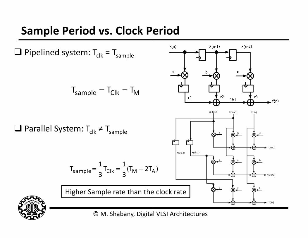
Sample Period vs. Clock Pe
Pipelined system: Tclk = Tsample
MClksample TTT
Parallel System: Tclk ≠ Tsamplep
112T(T
31
T31
T AMClksample
Higher Sample rate than the
© M. Shabany, Digital
Higher Sample rate than the
eriod
X(3k)
a b c
X(3k+1)X(3k+2)
Y(3k+2)
c a b
X(3k‐2) X(3k‐1)
Y(3k+1)
b c a
)A
clock rate
l VLSI Architectures
Y(3k)
clock rate
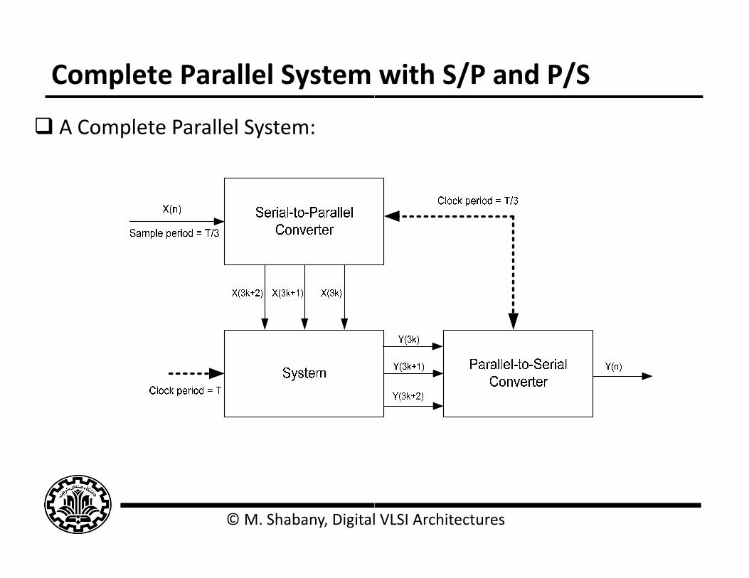
Complete Parallel System
A Complete Parallel System:
© M. Shabany, Digital
with S/P and P/S
l VLSI Architectures

S/P and P/S Blocks
S/P Converter:
© M. Shabany, Digital
P/S Converter:
Y(3k)Y(3k+1)Y(3k+2)
T T T
Y(n)
T
T/3T/3
Sample PeriT/3
T T
Parallel‐to‐Serial Converter
l VLSI Architectures

When Pipelining When Pa
Pipeline technique is used when th
(Number 1, 2, 3, 4)
Parallelism is used when the criticacommunication or I/O bound. (Numb Pipelining does not help in this cas
a.k.a Communication Bounded
3
Comb. Logic
1
2
531
4
© M. Shabany, Digital
arallelism?
he critical path is in the design
al path is bounded by the ber 5) se!
Comb. Logic
l VLSI Architectures