Embed Size (px)
Citation preview
i
DIGITAL TECHNIQUES FOR COMPENSATION OF THE
RADIO FREQUENCY IMPAIRMENTS IN MOBILE
COMMUNICATION TERMINALS
Master Thesis Performed in
Electronic Devices Division
By
Sudarshan Gandla
LiTH-ISY-EX--11/4530--SE
Linköping November 2011
Institutionen för systemteknik
Department of Electrical Engineering
Examensarbete
Linköpings tekniska högskola Linköpings universitet
581 83 Linköping
Department of Electrical Engineering Linköpings universitet SE-581 83 Linköping, Sweden
i
DIGITAL TECHNIQUES FOR COMPENSATION
OF THE RADIO FREQUENCY IMPAIRMENTS IN
MOBILE COMMUNICATION TERMINALS
Master Thesis Performed in
Electronic Devices Division
By
Sudarshan Gandla
LiTH-ISY-EX--11/4530--SE
Linköping November 2011
Communications Electronics, ISY
Master degree, 2011
ii
DIGITAL TECHNIQUES FOR COMPENSATION
OF THE RADIO FREQUENCY IMPAIRMENTS IN
MOBILE COMMUNICATION TERMINALS
By
Sudarshan Gandla
LiTH-ISY-EX--11/4530--SE
Supervisor: Dominique Nussbaum, Eurecom Research Institute & Graduate School,
France.
Examiner: Ted Johansson, Linköping University, Sweden.
iii
Presentation Date 2011-11-10
Publishing Date (Electronic version) 2011-11-25
Department and Division
Department of Electronic Devices
URL, Electronic Version http://urn.kb.se/resolve?urn=urn:nbn:se:liu:diva-72330
Publication Title Digital Techniques for Compensation of RF Impairments in Mobile Communication Terminals
Author(s) Sudarshan Gandla
Abstract: The 3G and 4G systems make use of spectrum efficient modulation techniques which has variable amplitude. The variable amplitude methods usually use carrier‟s amplitude and phase to carry the message signal. As the amplitude of the carrier signal is varied continuously, they are sensitive to the disturbances affecting the information signal by introducing nonlinearities. Nonlinearities not only introduce errors in the data but also lead to spreading of signal spectrum which in turn leads to the adjacent channel interference. In transmitters, the power amplifier (PA) is the main source for introducing nonlinearities in the system, further to this, analog implementation of Quadrature modulator suffers from many distortions, at the same time receiver also suffers from Quadrature demodulator impairments, in particular, gain and phase imbalances and dc-offset from local oscillator, which all together degrades the performance of mobile communication systems. The baseband digital predistortion technique is used for compensation of the Radio Frequency (RF) impairments in transceivers as it provides significant accuracy and flexibility. The Thesis work is organized in two phases: in the first phase, a bibliography on available references is documented and later a simulation chain for compensation of RF impairments in mobile terminal is developed using Matlab software. By using the loop back features of Lime LMS 6002D architecture, it is possible to separate the problems of the Quadrature modulator (QM) and Quadrature demodulator (QDM) errors from the rest of the RF impairments. However in the Thesis work Lime LMS 6002D chip wasn‟t used, as the work was optional. So, in the Thesis work, algorithm is developed in Matlab software by assuming the LMS 6002D architecture. The idea is performed by sequential compensation of all the RF impairments. At first the QM and QDM errors are compensated and later PA nonlinearities are compensated. The QM and QDM errors are compensated in a sequential way. At first the QM errors are compensated and later QDM errors are compensated. The QM errors are corrected adaptively by using a block called as Quadrature modulator correction by assuming an ideal QDM. Later, the QDM errors are compensated by using Hilbert filter with the pass band interval of 0.2 to 0.5. Later, the PAs nonlinearities are compensated adaptively by using a digital predistorter block. For finding the coefficients of predistorter, normalized least mean square algorithm is used. Improvement in adjacent channel power ratio (ACPR) of 13dB is achieved and signal is converging after 15k samples.
Keywords: Digital predistortion, linearization techniques, RF impairments, Mobile communications, NLMS
Language
X English Other (specify below)
Number of Pages 96
Type of Publication
Licentiate thesis X Degree thesis Thesis C-level Thesis D-level Report Other (specify below)
ISBN (Licentiate thesis)
ISRN:
Title of series (Licentiate thesis)
Series number/ISSN (Licentiate thesis)
iv
ABSTRACT
The 3G and 4G systems make use of spectrum efficient modulation techniques which has
variable amplitude. The variable amplitude methods usually use carrier‟s amplitude and phase to
carry the message signal. As the amplitude of the carrier signal is varied continuously, they are
sensitive to the disturbances affecting the information signal by introducing nonlinearities.
Nonlinearities not only introduce errors in the data but also lead to spreading of signal spectrum
which in turn leads to the adjacent channel interference. In transmitters, the power amplifier (PA)
is the main source for introducing nonlinearities in the system, further to this, analog
implementation of Quadrature modulator suffers from many distortions, at the same time receiver
also suffers from Quadrature demodulator impairments, in particular, gain and phase imbalances
and dc-offset from local oscillator, which all together degrades the performance of mobile
communication systems.
The baseband digital predistortion technique is used for compensation of the Radio Frequency
(RF) impairments in transceivers as it provides significant accuracy and flexibility.
The Thesis work is organized in two phases: in the first phase, a bibliography on available
references is documented and later a simulation chain for compensation of RF impairments in
mobile terminal is developed using Matlab software.
By using the loop back features of Lime LMS 6002D architecture, it is possible to separate the
problems of the Quadrature modulator (QM) and Quadrature demodulator (QDM) errors from the
rest of the RF impairments. However in the Thesis work Lime LMS 6002D chip wasn‟t used as
the work was optional. So, in the Thesis work, algorithm is developed in Matlab software by
assuming the LMS 6002D architecture.
The idea is performed by sequential compensation of all the RF impairments. At first the QM and
QDM errors are compensated and later PA nonlinearities are compensated. The QM and QDM
errors are compensated in a sequential way. At first the QM errors are compensated and later
QDM errors are compensated. The QM errors are corrected adaptively by using a block called as
Quadrature modulator correction by assuming an ideal QDM. Later, the QDM errors are
compensated by using Hilbert filter with the pass band interval of 0.2 to 0.5. Later, the PAs
nonlinearities are compensated adaptively by using a digital predistorter block. For finding the
coefficients of predistorter, normalized least mean square algorithm is used.
Improvement in adjacent channel power ratio (ACPR) of 13dB is achieved and signal is
converging after 15k samples.

v
ACKNOWLEDGMENT
First and the foremost, I would like to thank my supervisor Mr. Dominique Nussbaum, Eurecom
and my Professor Dr. Ted Johansson, Linköping University for giving me an opportunity to work
on digital techniques for compensation of the RF impairments in transceivers. I would like to
mention that their support is invaluable and they have patiently led me throughout my work.
Without their constant support this Thesis work wouldn‟t have been finished. Though working
with Mr. Dominique is for short period I have learnt many things from him, it was very nice to
work with him.
I would like to thank my professor Atila Alvandpour, the Head of the Department for the
Electronic Devices for designing the course work interestingly and helped in building a strong
career.
I would like to thank Eurecom, Linköping University and French Government for the financial
support. Thanks to my friends at FJT for cooking me delicious foods.
I would like thank my friend Jaya Krishna for encouraging me to accept the thesis work.
Last but not least, I would like say that support from my family is immeasurable under all the
circumstances.
vi
Contents CHAPTER 1: INTRODUCTION ON MODERN MOBILE COMMUNICATIONS SYSTEM
…………………………………………………………………………………………………1
1.1 Introduction...................................................................................................................... 1
1.2 Aim of the Thesis............................................................................................................. 3
1.3 Outline of the Thesis ........................................................................................................ 3
CHAPTER 2: GENERALITIES ON MODULATION TECHNIQUES, RADIO FREQUENCY
POWER AMPLIFIER DISTORTIONS, ANALOG IMPAIRMENTS AND QUANTIZATION
ERRORS ................................................................................................................................... 4
2.1 Digital Modulation Techniques For Non-Constant Envelope Signal .............................. 4
2.1.1 Multiple-Quadrature Amplitude Modulation (M-QAM) .......................................... 4
2.1.2 Orthogonal Frequency Division Multiplexing .......................................................... 4
2.2Classes of Amplifiers ........................................................................................................ 5
2.2.1 Class A Amplifier ..................................................................................................... 7
2.2.2 Class B Amplifier ..................................................................................................... 7
2.2.3 Class AB Amplifier ................................................................................................... 7
2.2.4 Class C Amplifier ..................................................................................................... 7
2.2.5 Class D, E, F and S Amplifier ................................................................................... 7
2.2.6 Conclusion ................................................................................................................ 7
2.3 Modeling of Power Amplifier ......................................................................................... 8
2.3.1SalehModel ................................................................................................................ 8
2.3.2 Rapp Model ............................................................................................................... 9
2.3.3 Ghorbani-Model ........................................................................................................ 9
2.4Modeling of the Power Amplifier with Memory effects .................................................. 9
2.4.1Volterra Series ........................................................................................................... 9
2.4.2Memory Polynomial ................................................................................................ 10
2.4.3Wiener, Hammerstein and Wiener Hammerstein Models ....................................... 10
2.5Analog Impairments ....................................................................................................... 11
2.6Quantization Errors ......................................................................................................... 11
CHAPTER 3: COMPENSATION OF RADIO FREQUENCY IMPAIRMENTS IN
TRANSCEIVERS ................................................................................................................... 12
3.1 Linearization Techniques............................................................................................... 12
vii
3.1.1Feedback .................................................................................................................. 12
3.1.2Feed Forward ........................................................................................................... 13
3.1.3Linear Amplification using Nonlinear Components (LINC) ................................... 13
3.1.4 Envelope Elimination Restoration (EER) Systems ................................................. 14
3.1.5 Predistortion ............................................................................................................ 14
3.2Implementation of Digital Predistortion ......................................................................... 16
3.2.1 Radio Frequency Digital Predistortion ................................................................... 16
3.2.2Baseband Digital Predistortion ................................................................................ 17
3.3 Factors limiting the Performance of Digital predistortion ............................................. 19
3.3.1 Amplifier Nonlinearity ............................................................................................ 19
3.3.2 Types of Memory Effects ....................................................................................... 20
3.3.3 in-Phase/Quadrature Imbalances ............................................................................ 20
3.4 Review of Interesting References on the Power Amplifier Nonlinearity and Analog
Imperfections ....................................................................................................................... 21
3.4.1References on the Digital Predistortion for the Power Amplifier ............................ 21
3.4.2References on the Power Amplifier with Memory Effects ...................................... 22
3.4.3References on In-phase/Quadrature,Local Oscillator Leakage, modulator and
demodulator errors in Transmitter and Receiver ............................................................. 23
3.4.4 References on joint compensation of the Power Amplifier Nonlinearity, the Quadrature
Modulator and Demodulator Errors ................................................................................. 24
CHAPTER 4: SIMULATION OF the DIGITAL PREDISTORTER .................................... 26
4.1 Simulation Chain ............................................................................................................... 26
Chapter 5: IMPLEMENTATIONOF ADAPTIVEDIGITAL PREDISTORTIONFOR RADIO
FREQUENCY IMPAIRMENTS COMPENSATION IN ACTUAL SYSTEMS. .................. 40
5.1Modeling ......................................................................................................................... 40
5.2Target to Achieve ........................................................................................................... 40
5.3 Description of System ................................................................................................... 41
5.4 Studying the Impairments caused by the QM and QDM errors .................................... 41
5.2.1 QM Impairment Implementation ............................................................................ 45
5.2.2 QDM error compensation ....................................................................................... 45
5.3 Adaptive Quadrature Modulator Error Compensation (Ideal Demodulator) ................ 46
5.4 Adaptive QM and QDM impairments compensation .................................................... 50
5.5 Adaptive PD for RF impairments compensation ........................................................... 54
Chapter 6: Conclusion and Future Work ................................................................................ 60

viii
REFERENCES ........................................................................................................................ 62
LIST OF SYMBOLS & ABBREVIATIONS ......................................................................... 65
APPENDIX ............................................................................................................................. 67
Compensation of RF Impairments ....................................................................................... 69
1.) Compensation of Modulator and Demodulator Errors: ..................................... 69
2.) Compensation of Power Amplifier Nonlinearity: ............................................. 77
LIME LMS6002D ............................................................................................................... 84
ix
List of Figures
Figure 1.1 Gain based digital predistortion ....................................................................................... 2
Figure 2.1 Generation of OFDM signal ............................................................................................ 5
Figure 2.2 AM-AM curve ................................................................................................................. 6
Figure 2.3 AM/PM curve .................................................................................................................. 6
Figure 2.4 Distortion representation using two-tone tests ................................................................. 8
Figure 2.5 Memory polynomial....................................................................................................... 10
Figure 2.6 Wiener model ................................................................................................................. 10
Figure 2.7 Hammerstein model ....................................................................................................... 10
Figure 2.8 Wiener Hammerstein model .......................................................................................... 11
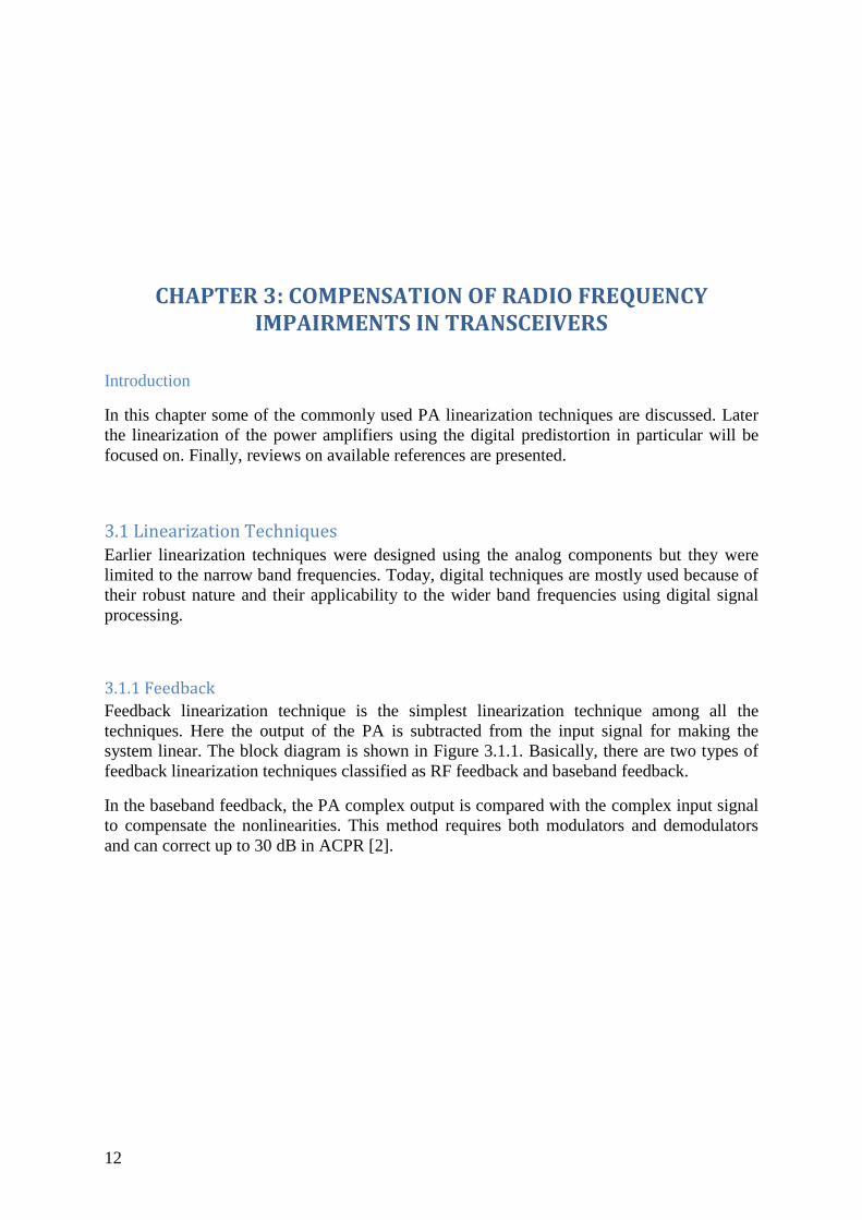
Figure 3.1 Baseband Cartesian Feedback Loop .............................................................................. 13
Figure 3.2Feedforward linearization ............................................................................................... 13
Figure 3.3 LINC transmitter ............................................................................................................ 14
Figure 3.4 Envelop Elimination and Restoration ............................................................................ 14
Figure 3.5 Cascading predistorter and power amplifier .................................................................. 14
Figure 3.6Transfer functions of PD, PA and cascaded stage .......................................................... 15
Figure 3.7 Pout vs. Pin of PA with PD ............................................................................................ 15
Figure 3.8 Analog baseband PD ...................................................................................................... 16
Figure 3.9 Digital baseband Predistortion ....................................................................................... 18
Figure 4.1 Adaptive PD for compensation of power amplifier nonlinearity................................... 26
Figure 4.2 AM/AM curves (ideal QM and QDM) .......................................................................... 28
Figure 4.3 AMPM curves (Ideal QM and QDM) ............................................................................ 29
Figure 4.4 PSD spectrums (ideal QM and QDM) ........................................................................... 29
Figure 4.5 MSE curve for ideal QM and QDM .............................................................................. 30
Figure 4.6 Adaptive PD for compensation of RF impairments (ideal demodulator) ...................... 30
Figure 4.7 AM/AM curves (ideal QDM) ........................................................................................ 32
Figure 4.8 AM/PM curves (ideal QDM) ......................................................................................... 33
Figure 4.9 PSD Spectrums (Ideal QDM) ........................................................................................ 33
Figure 4.10 MSE curve for RF impairments compensation (ideal QDM) ...................................... 34
Figure 4.11 Adaptive PD for RF impairments compensation (ideal modulator) ............................ 34
Figure 4.13 AM/AM curves for RF impairments compensation (ideal modulator) ....................... 37
Figure 4.14 AM/PM Curve for RF impairments compensation (ideal modulator) ......................... 37
Figure 4.16 PSD spectrums for RF impairments compensation (ideal modulator) ........................ 38
Figure 4.17 MSE Curve for RF impairments compensation (ideal modulator) .............................. 38
Figure 5.1 Functional Block Diagram ............................................................................................. 41
Figure 5.2 Baseband model ............................................................................................................. 42
Figure 5.3 Fundamental tone ........................................................................................................... 43
Figure 5.4 Output after Modulator errors ........................................................................................ 43
Figure 5.5 Signal at r(n) in dB ......................................................................................................... 44
Figure 5.6 Signal at z(n) .................................................................................................................. 44
Figure 5.7 Hilbert filter ................................................................................................................... 45
Figure 5.8 Signals at F (n) ............................................................................................................... 45
Figure 5.9 Adaptive QMC for compensation of modulator errors (ideal demodulator) ................. 46
x
Figure 5.10 before compensation of QM errors .............................................................................. 47
Figure 5.11 after Compensation of QM errors ................................................................................ 47
Figure 5.12 PSD before compensation of modulator errors ............................................................ 48
Figure 5.13 PSD after modulator errors compensation ................................................................... 49
Figure 5.14 MSE curve for modulator errors compensation ........................................................... 49
Figure 5.15 Adaptive QMC for compensation of modulator and demodulator errors .................... 50
Figure 5.16 before compensation of QM and QDM errors compensation ...................................... 51
Figure 5.17 after compensation of QM and QDM errors compensation......................................... 51
Figure 5.18 PSD before Compensation of Modulator and Demodulator errors ............................. 52
Figure 5.19 PSD after compensation of modulator and demodulator errors ................................... 53
Figure 5.20 Learning curvature ....................................................................................................... 53
Figure 5.21 Adaptive PD for compensation of RF impairments ..................................................... 54
Figure 5.22 before compensation of RF impairments ..................................................................... 55
Figure 5.23 after compensation of RF impairments ........................................................................ 55
Figure 5.24 AM/AM curve after RF impairments compensation ................................................... 57
Figure 5.25 AM/PM curve after RF impairments compensation .................................................... 57
Figure 5.26 PSD spectrums after RF impairments compensation ................................................... 58
Figure 5.27 MSE curve for RF impairments compensation ............................................................ 59
Figure A.1 LTE Signal in Frequency Domain ................................................................................ 69
Figure A.2 Adaptive Modulator and Demodulator Error Compensation ........................................ 70
Figure A.3Adaptive Quadrature Modulator Error Compensation................................................... 70
Figure A.4 Adaptive QM and QDM Error Compensation .............................................................. 71
Figure A.5 Adaptive PD for RF Impairments Compensation ......................................................... 77
Figure A.6 Functional Block Diagram of Lime LMS6002D .......................................................... 85
xi
List of Tables
Table 3.1 Compensation of nonlinearity in Memory less Nonlinearity .................................. 22
Table 3.2 the review of literature on nonlinearities of power amplifiers with memory .......... 22
Table 3.3 the review of literature on In-phase / Quadrature imbalances and LO leakages in TX and
RX. .......................................................................................................................................... 23
Table 3.4 Adaptive RF impairments Compensation in Transmitter and Demodulator Errors
Compensation at Receivers ..................................................................................................... 25
Table 4.1 EVM with and without DPD ................................................................................... 30
Table 4.2 EVM with and without RF Impairments Compensation ......................................... 34
Table 4.3 EVM with and without RF Impairments Compensation (Ideal Modulator) ........... 39
Table 5.1 difference in dB between Signal and Image signal before and after Modulator error
Compensation .......................................................................................................................... 47
Table 5.2 difference in dB between Signal and Image Signal before and after Compensation of
Modulator and Demodulator errors ......................................................................................... 52
Table 5.3 difference in between Signal and Image signal before and after Compensation of RF
Impairments ............................................................................................................................. 56
1
CHAPTER 1: INTRODUCTION ON MODERN MOBILE
COMMUNICATIONS SYSTEM
1.1 Introduction In the last few decades, the number of mobile users has been increasing which has lead to the
innovation of newer technologies for the means of reliable communications. For instance, in
global system for mobile communications (GSM) modulation technique used is frequency
modulation (FM) and Gaussian minimum shifting key (GMSK) as they have ability to with
stand against noise, nonlinearities and interference [1]. In the original GSM systems, the
nonlinearity is not a problem as envelope is kept at constant and the phase of the carrier is
modulated.
In recent years, the usage of internet in mobiles has been growing, leading to the
development of 3G and 4G systems. These systems needs higher amount of data transferring
as it gives an option to user on video calling, emails and high resolution photographs. These
systems make use of spectrum efficient modulation techniques which have variable
amplitude [2]. The variable amplitude methods usually use carrier‟s amplitude and phase to
carry the message signal. As the amplitude of the carrier signal varied continuously that are
sensitive to the disturbances affecting the information signal by introducing nonlinearities.
Nonlinearities can be understood as differences in between the input and output signal due to
the addition of newer signals. They not only introduce errors in the data but also lead to
spreading of signal spectrum which in turn leads to the adjacent channel interference.
In general, nonlinearities are caused by the power amplifiers (PA) and are high at higher
power region. In addition to the PA nonlinearities, analog implementation of the Quadrature
modulator (QM) and Quadrature demodulator (QDM) suffers from many distortions. At
transmitter, the QM errors can result in generation of inter-modulation products which in turn
causes adjacent channel interference. In addition to above distortions, the Radio Frequency
(RF) filters have non-ideal response which can further degrade the performance of system.
This thesis discusses digital techniques for compensation of the Radio Frequency
impairments in for modern communication systems.
To reduce the nonlinearities, the input power has to be reduced so that the power amplifier
will be operated in the linear region, which is called as output back off, but this degrades the
efficiency of system. Linearity and efficiency goes in opposite way, so if a system is highly
linear its efficiency is less. So, the system has to be modeled in such a way that it should be
highly linear at the same time has moderate efficiency.
Several linearization techniques for the power amplifier are available, however in this thesis,
we focus on the baseband digital predistortion (DPD) because it provides significant accuracy
and flexibility.
2
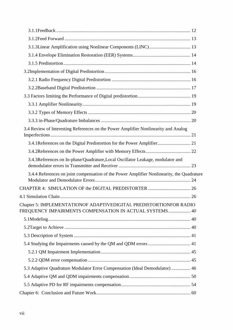
The idea behind predistortion is that a non-linear block called as predistorter (PD) whose
transfer function is the inverse of the PA is cascaded along with the power amplifier to make
the output linear. Here the gain of PD increases when the gain of the power amplifier
decreases and phase of PD is negative to phase of the power amplifier. So that net result of
gain and phase of two devices in cascade becomes constant.
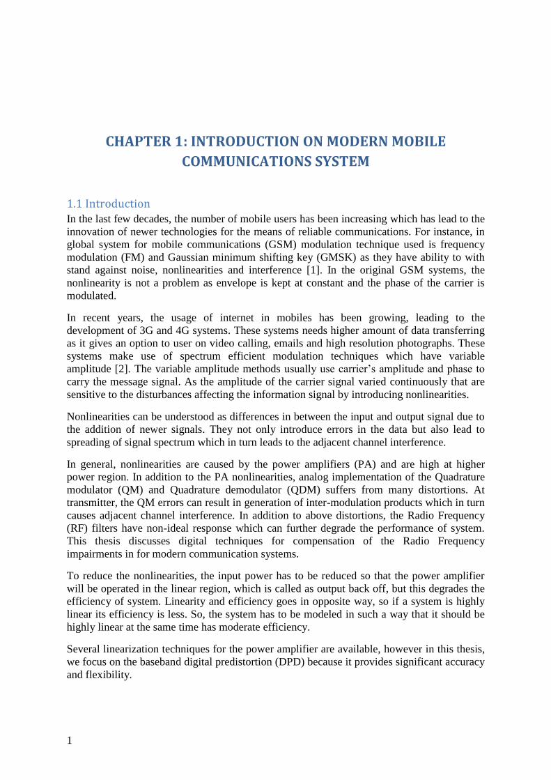
The block diagram of gain based baseband digital predistorter (PD) is shown in the Figure
1.1.
Figure 1.1 Gain based digital predistortion
The complex multiplier is used to multiple the complex input signals (digital signal) with the
PD gain followed by a digital-to-analog (DAC) converter and a reconstruction filter. The
baseband signal is up-converted into radio frequency by the Quadrature modulator (QM). To
compensate the nonlinearities of the power amplifier we need a feedback (FB) signal from
the output of a power amplifier, which can be done by using the Quadrature demodulator
(QDM). The QDM converts the radio frequency back to baseband frequency, an anti-aliasing
filter is used to reject the unwanted frequencies and then it is forwarded to the analog-to-
digital converter (ADC). Adaptation of PD is done using a feedback loop and coefficients of
PD are updated by using indirect learning algorithm.
In addition to the PA nonlinearity, the QM and QDM suffer from LO leakage, amplitude and
phase imbalances, there by affecting the performance of DPD. Unfortunately, most of the RF
power amplifiers have some degree of memory effects, which means that their output will not
only depend on the current input but also on the past input. This is because the output signal
will be affected by the frequency of the signal and temperature. So, for the wider band and
high power systems memory effects should be taken into account.
Further the performance of the DPD also depends on the quantization error in the ADC and
DAC.
3
The nonlinearity of a power amplifier can be modeled by using several methods, such as,
third order input intercept point (IIP3), total harmonic distortion (THD), adjacent channel
power ratio (ACPR) and error vector magnitude (EVM). In this thesis ACPR is used for
measuring the nonlinearities of a power amplifier.
ACPR is defined as the part of the signal power that lands on the adjacent signal band in
relation to the signal power on the signal band and is expressed in dB.
𝐴𝐶𝑃𝑅 = 10𝑙𝑜𝑔𝑃𝑎𝑑𝑗𝑎𝑐𝑒𝑛𝑡
𝑃𝑠𝑖𝑔𝑛𝑎 𝑙. (2.1)
1.2 Aim of the Thesis Transmitter suffers from the power amplifier nonlinearities, analog QM impairments and
receiver also suffers from QDM impairments which all together degrade the performance of
the mobile communication systems.
As far as authors best knowledge, only a few examples are available from the references
which have developed has developed an adaptive algorithm for the RF impairments
compensation in the transmitter where has demodulation errors at the receivers are
compensated separately. So, the idea of thesis is to develop digital techniques for
compensating the radio frequency impairments in mobile communication in transceivers
using MATLAB software.
1.3 Outline of the Thesis
The thesis work is presented in five chapters:
Chapter1 gives a short description about the modern mobile communication systems.
In chapter 2, an introduction about modern modulation techniques and various models of the
power amplifiers are presented and the later part describes modeling of the PA with and
without memory effects.
In chapter 3, a brief summary on the various kinds of linearization techniques for the power
amplifiers are presented along with their advantages, disadvantages and correction ability.
However, in this thesis we focus on the DPD linearization technique by compensating the RF
impairments in transceivers. Finally, review on available references on compensation of the
RF impairments is presented.
In chapter 4, implementation and simulation chain from the references [25, 32 and 35] are
developed for studying the effects on RF impairments and their compensation algorithm are
presented.
In chapter 5, implementation of the adaptive PD for the RF impairments compensation in
actual system is presented.
4
CHAPTER 2: GENERALITIES ON MODULATION TECHNIQUES,
RADIO FREQUENCY POWER AMPLIFIER DISTORTIONS,
ANALOG IMPAIRMENTS AND QUANTIZATION ERRORS
In chapter 2, an introduction about digital modulation techniques and various classes of the
linear power amplifiers (like A, B, AB), class C and the switching amplifiers (like D, E, F
and S) are discussed at first and later it extends the discussion on modeling of the PA with
and without memory effects.
A brief introduction about the limiting factors for reliable mobile communications systems
like amplitude imbalance, phase imbalance, LO leakage, ADC and DAC quantization errors
are presented.
2.1 Digital Modulation Techniques For Non-Constant Envelope Signal Current and future planned mobile communication systems use the digital modulations
techniques having non-constant signal envelope. This is due to their ability to increase the
data transmission speed.
2.1.1 Multiple-Quadrature Amplitude Modulation (M-QAM)
In the Quadrature amplitude modulation (QAM), the signal points in the two-dimensional
signal space diagram are distributed on a square lattice. The most commonly used M-QAM is
16-QAM, 64-QAM, 128-QAM and 256-QAM respectively. By using higher-order
constellation, it is possible to transmit more bits per symbol. The points that are closer
together are more susceptible to noise. These results in a higher bit error rate and so the
higher-order QAM can deliver more data and are less reliable than lower-order QAM.
2.1.2 Orthogonal Frequency Division Multiplexing
The orthogonal frequency division multiplexing (OFDM) is a multicarrier modulation
technique, which is based on the idea of dividing a given high-bit-rate data stream into
several parallel lower bit-rate streams and modulating each stream on separate carriers often
called subcarriers or tones.The most attractive feature is its high spectral efficiency (due to
the orthogonality of the sub-carriers) and it is particularly suited for frequency selective
channels.
5
Cyclic prefix is technique in which for each symbol, some samples from the end are
appended to the beginning of the symbol to absorb the echo delays of the multipath channel
and to allow easy equalization. Cyclic prefix transforms a frequency selective channel into a
set of flat fading channels. Often the signal time is lengthened, by a so-called guard interval,
to combat inter symbol interference due to the linear filtering property. The guard interval is
chosen to be at-least as long as the duration of the impulse response of the channel.
The carrier frequency is given by
Fk = f0 + K
T , 0<K<N/2 where N is an even integer (2.1)
f0 is the base frequency is chosen such that 2f0 is an integer.
For 0<=k<N/2, the OFDM signal is given by
( 𝑆 𝑡 = s2𝑘 cos(2πfkt) − 𝑠2𝑘 sin( 2πfk t ),𝑁/2
𝑘=0 0<=t<T (2.2)
= 0, else)
The coefficients s2𝑘and s2𝑘+1are chosen for every k from some two dimensional modulation
schemes, which is often QAM.
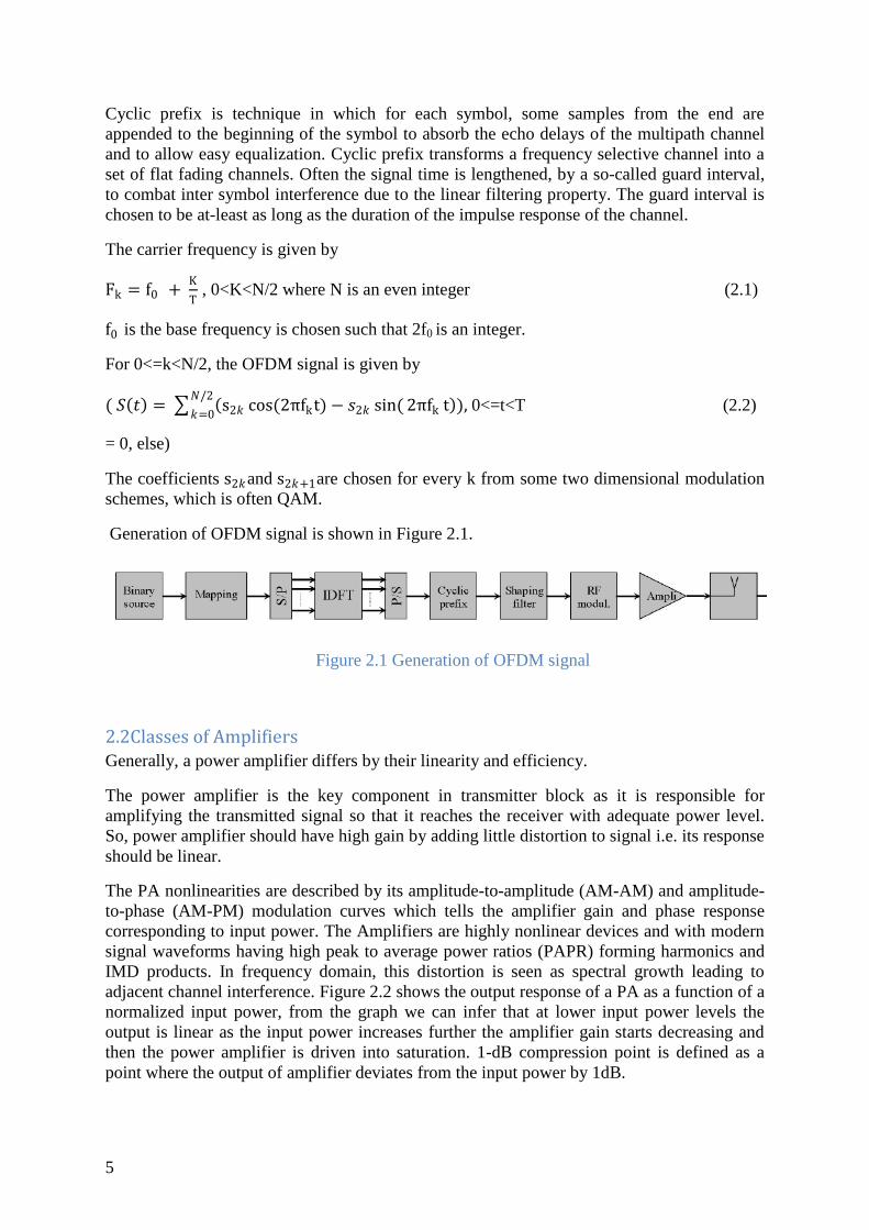
Generation of OFDM signal is shown in Figure 2.1.
Figure 2.1 Generation of OFDM signal
2.2Classes of Amplifiers Generally, a power amplifier differs by their linearity and efficiency.
The power amplifier is the key component in transmitter block as it is responsible for
amplifying the transmitted signal so that it reaches the receiver with adequate power level.
So, power amplifier should have high gain by adding little distortion to signal i.e. its response
should be linear.
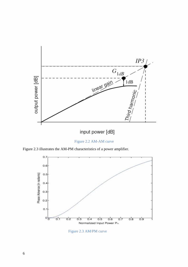
The PA nonlinearities are described by its amplitude-to-amplitude (AM-AM) and amplitude-
to-phase (AM-PM) modulation curves which tells the amplifier gain and phase response
corresponding to input power. The Amplifiers are highly nonlinear devices and with modern
signal waveforms having high peak to average power ratios (PAPR) forming harmonics and
IMD products. In frequency domain, this distortion is seen as spectral growth leading to
adjacent channel interference. Figure 2.2 shows the output response of a PA as a function of a
normalized input power, from the graph we can infer that at lower input power levels the
output is linear as the input power increases further the amplifier gain starts decreasing and
then the power amplifier is driven into saturation. 1-dB compression point is defined as a
point where the output of amplifier deviates from the input power by 1dB.
6
Figure 2.2 AM-AM curve
Figure 2.3 illustrates the AM-PM characteristics of a power amplifier.
Figure 2.3 AM/PM curve

7
2.2.1 Class A Amplifier
In the class A amplifier, the conduction angle is 360˚, it means that transistor is conductive in
each full signal cycle. In this, amplifier nonlinearity is introduced only at high amplitudes [3]
as the transistor is used far from the cut off. However, efficiency of the amplifier is limited to
50% as the DC operating point is chosen half way of linear region to avoid distortion during
signal swing.
2.2.2 Class B Amplifier
In class B amplifier, to increase the efficiency, the conduction angle is chosen as 180˚ and is
push-pull stage. Here maximum efficiency achieved is 78.5% [4] however it needs two
identical transistors in anti phase and a BALUN at both input and output.
2.2.3 Class AB Amplifier
In general, the class B amplifier is linear only in ideal conditions as there is source of small
signal nonlinearity called as crossover distortion [2]. By choosing the conduction angle
slightly greater than 180˚ cross over distortion can be overcome and it is called as the AB
class amplifier. In this amplifier, efficiency is lesser when compared to class B but more
linear than the class B.
The class B and AB amplifiers have transistors biased in such a way that transistors come
near to cut off at low amplitudes [3, 5] and there they exhibit nonlinearities. If the class B and
AB amplifiers are used with high back-off nonlinearities can be seen only at lower
amplitudes.
2.2.4 Class C Amplifier
In the class C amplifier the conduction angle is less than 180˚, in this mode linearity is lost
but the efficiency is high.
2.2.5 Class D, E, F and S Amplifier
In these amplifiers classes, efficiency is very high but linearity is lost due to switching of
transistors states. For these classes of the amplifiers, amplitude modulation at input cannot be
preserved at output however phase modulation signals can be handled efficiently.
2.2.6 Conclusion
The class A, B and AB are fairly linear mode amplifiers with low to moderate efficiency. In
these amplifiers both current and voltage are conducted for at least half of signal cycle, in the
class C amplifier, higher the efficiency is achieved at cost of loosing linearity and output
power. The amplifiers like D, E, F and S are switching amplifiers that switch PA into on and
off state leading to nonlinearities but their efficiency are very high.

8
2.3 Modeling of Power Amplifier The general way of describing the nonlinear power amplifier is by using a polynomial
function [6].
𝑉𝑜𝑢𝑡 = anVpd |Vpd |n−1𝑁
𝑛=1 (2.3)
where 𝑉𝑃𝐷 is the predistortion output voltage or the PA input voltage 𝑉𝑜𝑢𝑡 is the PA output
voltage and 𝑎𝑛 is the distortion coefficient. The values of distortion coefficient are found by
using least square fit amplitude. Distortions can be observed using two-tone test, by taking
two closer frequencies ω1 and ω2. The output will contain the two tones plus new signals of
different frequencies. Figure 2.4 shows distortion produced which are inter-modulation
distortion products (IMD).
Figure 2.4Distortion representation using two-tone tests
The frequencies 2ω1 – ω2 and ω1 - 2ω2 are called third order IMD and these products are
major problems in the communication systems as they fall closer to the fundamental
frequencies and it is difficult to remove them by filtering.
The modelling ability of the PA with polynomial model is good only when the polynomial
order is high but this increases complexity. So, several models have been proposed and are
suitable for different types of applications.
2.3.1 SalehModel
The Saleh model [7] is commonly used the PA model and is specially designed for travelling
wave tube (TWT):
𝐺𝑃𝐴 VPD = aA |VPD |
1+bA |VPD | 2 , (2.4)
Ø𝑃𝐴 VPD = aØ|VPD |2
1+bØ|VPD | 2 . (2.5)
𝑎𝐴, 𝑎ø,𝑏𝐴 and 𝑏øare the distortion coefficients and the values of distortion coefficients [7] are
𝑎𝐴= 2.1587, 𝑎ø= 4.033, , 𝑏𝐴 = 1.1587, 𝑏ø= 9.104 respectively.
9
2.3.2 Rapp Model
The Rapp model [8] is designed for the solid state power amplifier.
The gain function is
𝐺𝑃𝐴 VPD = 1
(1+ VPD
aA
2b A) 1/2b A
. (2.5)
This model exhibits linear behaviour only at low amplitude levels.
2.3.3 Ghorbani-Model
The Ghorbani model is a PA model designed for solid state PAs. The gain and phase
functions are [9].
𝐺𝑃𝐴 VPD = aA |V in cA |
( 1+bA V in cA ) + dA vin , (2.6)
Ø𝑃𝐴 VPD = aØ|V in cØ|
( 1+bØ V in cØ ) + dØ vin . (2.7)
𝑎𝐴 ,𝑎Ø, 𝑏𝐴, 𝑏Ø, 𝑐𝐴 , 𝑐Ø,𝑑𝐴 𝑎𝑛𝑑 𝑑Øare the nonlinearity parameters. The values for parameter [9]
areaA= 8.1081, aØ= 4.6645, bA = 1.5413, bØ= 2.0965, cA= 6.5202, cØ= 10.88,
dA = -0.0718 and dØ= -0.003 respectively. This model is suitable for the FET amplifiers.
2.4Modeling of the Power Amplifier with Memory effects Unfortunately, most of the RF power amplifiers have some degree of memory effects, which
means that their output will not only depend on the current input but also on the past input.
This is because the output signal will be affected by the frequency of the signal and
temperature. So, for wider band and high power systems the memory effects should be taken
into account. The memory effects are basically frequency-domain fluctuations in the transfer
function or time dependent of the transfer function of power amplifier.
The PA model should have time dependent components to include the memory effects. There
are several methods to model a PAs with memory effects.
2.4.1Volterra Series
The Volterra series is a multivariate polynomial series of current and previous signal values
[10]. The series is
𝑉𝑃𝐴 𝑡 = … . .𝑚𝑚=1
𝐾𝑘=1 𝑘
𝑚𝑘𝑚𝑘=1
𝑚1 … . .𝑚𝑘 𝑣𝑝𝑑𝑘𝑙=1 𝑡 − 𝑚𝑙𝑡𝑠 . (2.8)
where, mk are the delays in discrete time, hk ( m1,........,mk) are the term coefficients, vpd is the
PA input, 𝑡𝑠 is the time step, M is the number of delays, and k is the order of polynomial.

10
Coefficients of the predistorter can be found by using Recursive least squares (RLS) method.
Accuracy can be increased by increasing K and M but this leads to complexity.
2.4.2 Memory Polynomial
The memory polynomial simplifies the Volterra series by exploiting the fact that the
nonlinearities in the PA are almost completely phase independent. Thus the baseband
Volterra series can be simplified to contain only powers of |Vpd| still retaining the accuracy of
the Volterra series and is better than the Wiener and Hammerstein models.
The equation of the memory polynomial model can be written as
𝑦 𝑠 = akl𝑀−1𝑙=0
𝐾−1𝑘=0 𝑥 𝑡 − 𝑚𝑙 𝑡𝑠 𝑥 𝑡 − 𝑚𝑙 𝑡𝑠 |𝑘 . (2.9)
Figure 2.5 Memory polynomial
2.4.3Wiener, Hammerstein and Wiener Hammerstein Models
The problem usually encountered with the Volterra series is computational complexity due to
the handling large number of parameters. The Wiener and Hammerstein models reduce the
Volterra series complexity.
The Wiener model [11] consists of a linear dynamic system (digital filter) followed by a
static nonlinearity. Block diagram is shown in Figure 2.6.
Figure 2.6 Wiener model
The Hammerstein model [11] consists of static nonlinearity followed by an IIR filter. Block
diagram is shown in Figure 2.7.
Figure 2.7 Hammerstein model
11
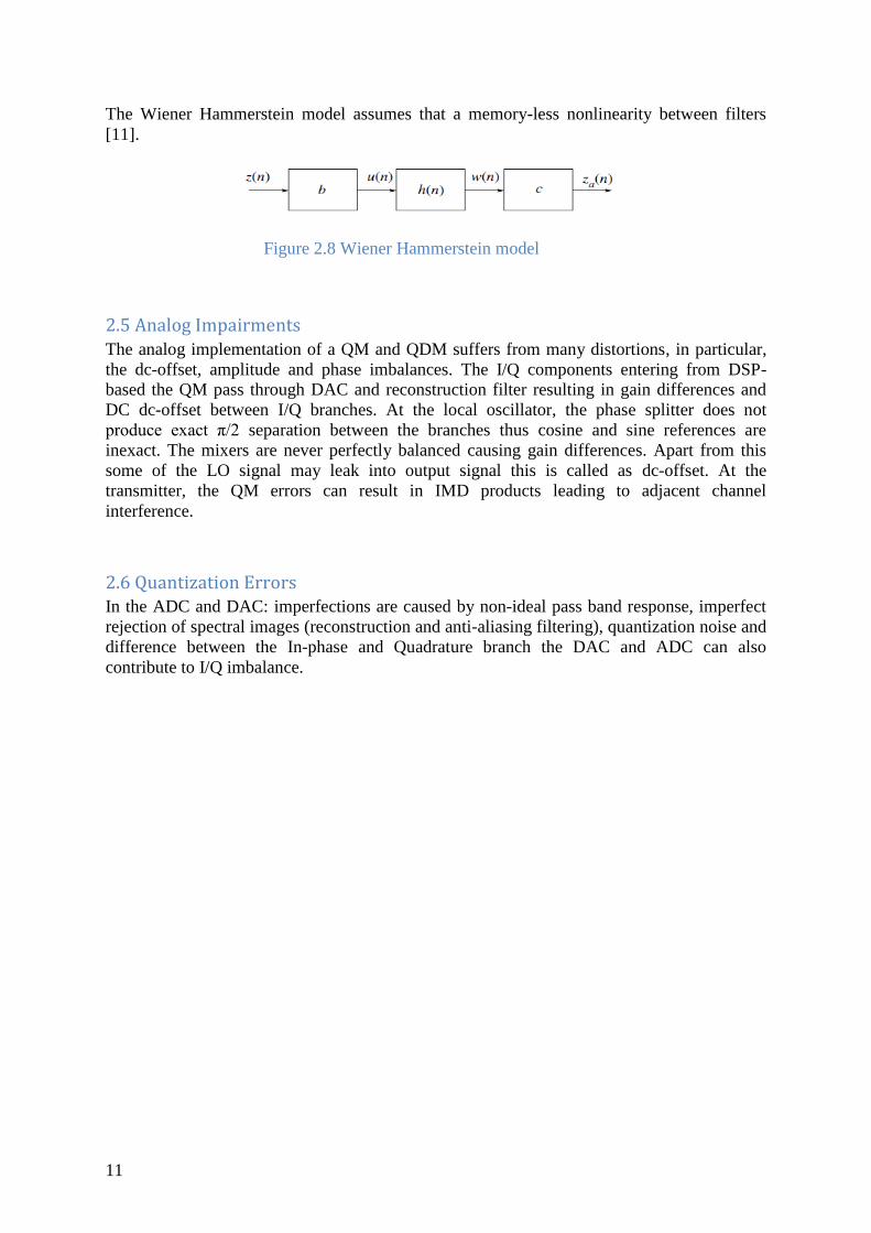
The Wiener Hammerstein model assumes that a memory-less nonlinearity between filters
[11].
Figure 2.8 Wiener Hammerstein model
2.5 Analog Impairments The analog implementation of a QM and QDM suffers from many distortions, in particular,
the dc-offset, amplitude and phase imbalances. The I/Q components entering from DSP-
based the QM pass through DAC and reconstruction filter resulting in gain differences and
DC dc-offset between I/Q branches. At the local oscillator, the phase splitter does not
produce exact π/2 separation between the branches thus cosine and sine references are
inexact. The mixers are never perfectly balanced causing gain differences. Apart from this
some of the LO signal may leak into output signal this is called as dc-offset. At the
transmitter, the QM errors can result in IMD products leading to adjacent channel
interference.
2.6 Quantization Errors In the ADC and DAC: imperfections are caused by non-ideal pass band response, imperfect
rejection of spectral images (reconstruction and anti-aliasing filtering), quantization noise and
difference between the In-phase and Quadrature branch the DAC and ADC can also
contribute to I/Q imbalance.
12
CHAPTER 3: COMPENSATION OF RADIO FREQUENCY IMPAIRMENTS IN TRANSCEIVERS
Introduction
In this chapter some of the commonly used PA linearization techniques are discussed. Later
the linearization of the power amplifiers using the digital predistortion in particular will be
focused on. Finally, reviews on available references are presented.
3.1 Linearization Techniques Earlier linearization techniques were designed using the analog components but they were
limited to the narrow band frequencies. Today, digital techniques are mostly used because of
their robust nature and their applicability to the wider band frequencies using digital signal
processing.
3.1.1 Feedback
Feedback linearization technique is the simplest linearization technique among all the
techniques. Here the output of the PA is subtracted from the input signal for making the
system linear. The block diagram is shown in Figure 3.1.1. Basically, there are two types of
feedback linearization techniques classified as RF feedback and baseband feedback.
In the baseband feedback, the PA complex output is compared with the complex input signal
to compensate the nonlinearities. This method requires both modulators and demodulators
and can correct up to 30 dB in ACPR [2].
13
Figure 3.1 Baseband Cartesian Feedback Loop
In RF feedback, the PA output is compared with the RF input signal. This method is suitable
only for lower frequencies as FB systems are unstable at higher frequencies [2].
The drawback of feedback linearization technique is that it cannot distinguish the
nonlinearities caused in feedback paths and nonlinearities caused by the PA.
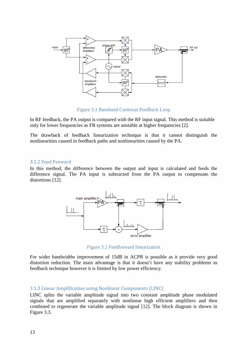
3.1.2 Feed Forward
In this method, the difference between the output and input is calculated and feeds the
difference signal. The PA input is subtracted from the PA output to compensate the
distortions [12].
Figure 3.2 Feedforward linearization
For wider bandwidths improvement of 15dB in ACPR is possible as it provide very good
distortion reduction. The main advantage is that it doesn‟t have any stability problems as
feedback technique however it is limited by low power efficiency.
3.1.3 Linear Amplification using Nonlinear Components (LINC)
LINC splits the variable amplitude signal into two constant amplitude phase modulated
signals that are amplified separately with nonlinear high efficient amplifiers and then
combined to regenerate the variable amplitude signal [12]. The block diagram is shown in
Figure 3.3.
14
Figure 3.3 LINC transmitter
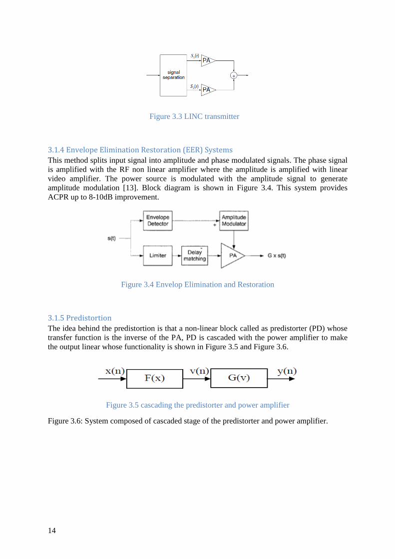
3.1.4 Envelope Elimination Restoration (EER) Systems
This method splits input signal into amplitude and phase modulated signals. The phase signal
is amplified with the RF non linear amplifier where the amplitude is amplified with linear
video amplifier. The power source is modulated with the amplitude signal to generate
amplitude modulation [13]. Block diagram is shown in Figure 3.4. This system provides
ACPR up to 8-10dB improvement.
Figure 3.4 Envelop Elimination and Restoration
3.1.5 Predistortion
The idea behind the predistortion is that a non-linear block called as predistorter (PD) whose
transfer function is the inverse of the PA, PD is cascaded with the power amplifier to make
the output linear whose functionality is shown in Figure 3.5 and Figure 3.6.
Figure 3.5 cascading the predistorter and power amplifier
Figure 3.6: System composed of cascaded stage of the predistorter and power amplifier.

15
Figure 3.6 Transfer functions of the PD, PA and cascaded stage
The relation between input and output of a power amplifier is shown in Figure 3.7. The
darker curve in the graph shows the nonlinearity of a power amplifier and we get linear
output when the PD is introduced.
Figure 3.7 Pout vs. Pin of PA with PD
Here, the correction for amplitude (AM/AM) is done by addition or subtraction of the
predistorter with the input of the power amplifier amplitude to make it linear or constant.
Similarly, the correction for phase (AM/PM) is done by adding the phase of the predistorter
to the power amplifier, whose phase is negative to the power amplifier, so that, the resultant
phase is zero.
The predistorter is classified into the analog predistorter and digital predistorter.
In the Analog PD, analog components are used where as in the digital PD, digital components
are used.
3.1.5.1 Analog Predistortion
The analog predistorter can be realized in two different ways: baseband analog PD and RF
analog PD.
The baseband PD is shown in Figure 3.8.

16
Figure 3.8 Analog baseband PD
The analog PD are simple to design, consumes less power, low cost to design and wide band
signal handling capability. However they provide moderate linearization and introduce
insertion loss to the system. Using the analog PD improvement in ACPR of about 10dB is
achieved [13].
3.1.5.2 Digital Predistortion
Similar to the analog PD, this can be realized either at the baseband or at RF.
The advantage of the digital predistortion (DPD) is that it does not depend on the operating
frequency of system like feed forward or analog PD techniques. So, therefore, this system is
well suited for software defined radio applications in which a wide range of frequency is
covered with single set of RF hardware.
As the digital PD is realized with the digital components the system is more flexible when
compared to the analog PD but its hardware is complex.
The important paths in the digital PD are forward and feedback path. Forward path has to
operate continuously where as the feedback can be operated when it is required depending
upon other factors. So, therefore the designing of forward path is crucial.
Using the digital PD a precise linearization is possible.
3.2Implementation of Digital Predistortion The digital predistortion can be implemented either at the baseband or at RF.
3.2.1 Radio Frequency Digital Predistortion
The important feature of the RF DPD is that: it does not dependent on the exact carrier
frequency of the signal or the baseband circuitry. Keeping this thing in mind, it is possible to
design a separate the PD chip or PA chip that includes PD.
RF DPD can be implemented either using phase and amplitude modulators or by QM.
In polar form, it uses both amplitude and phase modulators to correct amplitude distortions
and phase distortions separately. Here, operation takes place by considering both amplitude
and phase errors are independent to each other but in real both are inter-dependent.
17
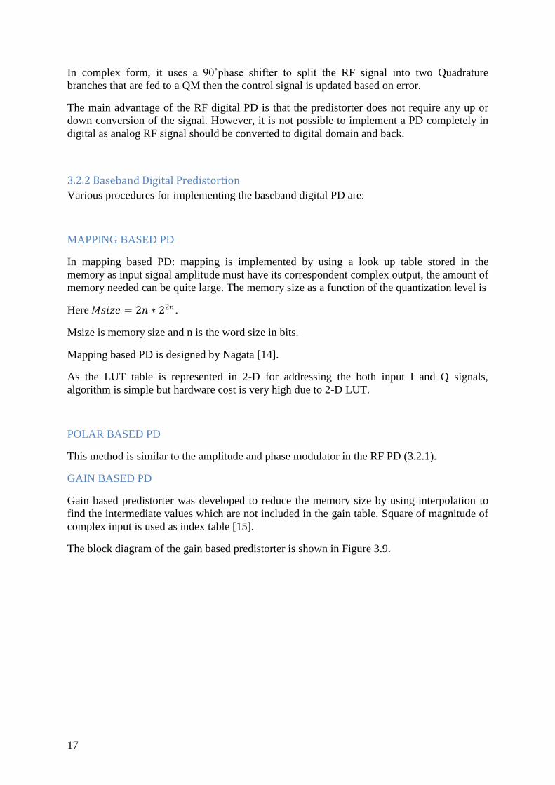
In complex form, it uses a 90˚phase shifter to split the RF signal into two Quadrature
branches that are fed to a QM then the control signal is updated based on error.
The main advantage of the RF digital PD is that the predistorter does not require any up or
down conversion of the signal. However, it is not possible to implement a PD completely in
digital as analog RF signal should be converted to digital domain and back.
3.2.2 Baseband Digital Predistortion
Various procedures for implementing the baseband digital PD are:
MAPPING BASED PD
In mapping based PD: mapping is implemented by using a look up table stored in the
memory as input signal amplitude must have its correspondent complex output, the amount of
memory needed can be quite large. The memory size as a function of the quantization level is
Here 𝑀𝑠𝑖𝑧𝑒 = 2𝑛 ∗ 22𝑛 .
Msize is memory size and n is the word size in bits.
Mapping based PD is designed by Nagata [14].
As the LUT table is represented in 2-D for addressing the both input I and Q signals,
algorithm is simple but hardware cost is very high due to 2-D LUT.
POLAR BASED PD
This method is similar to the amplitude and phase modulator in the RF PD (3.2.1).
GAIN BASED PD
Gain based predistorter was developed to reduce the memory size by using interpolation to
find the intermediate values which are not included in the gain table. Square of magnitude of
complex input is used as index table [15].
The block diagram of the gain based predistorter is shown in Figure 3.9.
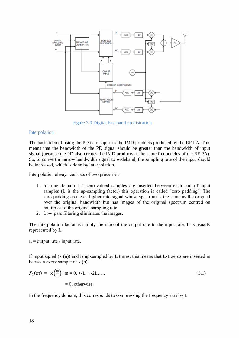
18
Figure 3.9 Digital baseband predistortion
Interpolation
The basic idea of using the PD is to suppress the IMD products produced by the RF PA. This
means that the bandwidth of the PD signal should be greater than the bandwidth of input
signal (because the PD also creates the IMD products at the same frequencies of the RF PA).
So, to convert a narrow bandwidth signal to wideband, the sampling rate of the input should
be increased, which is done by interpolation.
Interpolation always consists of two processes:
1. In time domain L-1 zero-valued samples are inserted between each pair of input
samples (L is the up-sampling factor) this operation is called "zero padding". The
zero-padding creates a higher-rate signal whose spectrum is the same as the original
over the original bandwidth but has images of the original spectrum centred on
multiples of the original sampling rate.
2. Low-pass filtering eliminates the images.
The interpolation factor is simply the ratio of the output rate to the input rate. It is usually
represented by L,
L = output rate / input rate.
If input signal (x (n)) and is up-sampled by L times, this means that L-1 zeros are inserted in
between every sample of x (n).
𝑋1 𝑚 = x m
L , m = 0, +-L, +-2L…., (3.1)
= 0, otherwise
In the frequency domain, this corresponds to compressing the frequency axis by L.

19
In order to increase the sampling frequency without aliasing, all the spectral components
should be removed other than those centered at ωT1 = 0 and ωT1 = π which can be achieved
by using a digital filter.
Magnitude Generator
Here the magnitude of complex input signal is squared and is used for indexing in look-up-
table.
Complex Multiplier
The complex multiplier is used to multiple the complex input signals with the predistortion
gain and is converted into analog signal by using a DAC. The DAC is followed by a
reconstruction filter to reject the image signals. The baseband signal is converted into the
radio frequency by using a QM. For the PD to be adapted automatically it should have a
feedback loop, the QDM is used to convert it into baseband signal, the QDM is followed by
an ADC.
3.3 Factors limiting the Performance of the Digital Predistortion The several factors limiting the performance of the DPD are the PA nonlinearity, QM, QDM
errors, ADC and DAC offset errors, LO leakage, filter errors and memory effects.
Power amplifiers: imperfections are various nonlinear distortion effects, like in-band
interference, spectral re-growth, inter-modulation distortions, together with memory
related effects.
The QM and QDM errors are gain imbalance and phase imbalance.
The DAC and ADC: imperfections are due non-ideal pass band response, imperfect
rejection of spectral images (reconstruction and anti aliasing filtering), quantization
noise and difference between the In-phase and Quadrature branch. The DAC and
ADC can also contribute to In-phase/Quadrature imbalances.
Oscillators: phase noise due to random fluctuations of oscillator phase, frequency and
phase oscillators and LO leakage.
Receiver amplification stages (LNA): even this can produce nonlinear amplification
distortions and can cause IMD products.
3.3.1 Amplifier Nonlinearity
The procedure for compensation the PA nonlinearities is discussed more in 3.6.
The impact of different the RF impairments is also heavily dependent on the used radio
architecture. Most of the radio devices are built on direct conversion (zero-IF) or low IF
principle in both transmitter and receiver implementations. However, the direct conversion is
more advantageous because of less hardware complexity and it eliminates the component like
image rejection filter. The receiver side is conceptually more challenging, since, the received
desired signals are typically weak and need to be processed and detected in the presence of
stronger signals in adjacent channels as well as strong out-of-band signals.
20
3.3.2 Types of the Memory Effects
Electrical memory effects: main sources for the electrical memory effects are due to
capacitances and inductances in the amplifier chain or frequency dependent impedances in
PA chain [10].
Thermal memory effects: main source for the thermal memory effects are due to thermal
fluctuations of the PA due the signal level [10]. The dissipated power in the PA changes with
the input signal level due to the rise of temperature of the transistors leading to distortions.
Generally, electrical memory effects are present in wide band signals (BW > 5MHz).In
narrow band signals (BW < 1MHz) the system is affected by the thermal memory effects.
3.3.3 In-Phase/Quadrature Imbalances
A multicarrier modulation technique such as OFDM (orthogonal frequency division
multiplexing) system supports many wireless communication standards, for example
WLANs, WIMAX and DVB-T. The direct conversion (zero IF) architecture is suitable
frontend architecture for such systems [16]. However, most of the transceivers and direct
conversion designs in particular are highly sensitive to the nonlinear distortion introduced by
the power amplifier. This is due to its non constant envelope and high peak-to-average ratio
(PAR) values and it also depends on the analog implementation of modulators and
demodulators.
The definitions [17] of these errors are defined as:
Gain imbalance, G is the ratio of gain in I branch to the gain in Q branch.
𝐺 =𝑔𝐼
𝑔𝑄, (3.2)
G is expressed in dB as 20logG.
The phase imbalance „Q‟ is the phase difference relative to π/2 between the two branches.
𝑄 =Φ𝐼
Φ𝑄. (3.3)
The LO leakage L is the ratio total power of the dc offset (𝑐𝐼2 + 𝑐𝑄
2) to power of complex
input amplitude (𝑔𝐼2 + 𝑔𝑄
2).
𝐿 =2( 𝑐𝐼
2+ 𝑐𝑄2)
𝑔𝐼2+ 𝑔𝑄
2 . (3.4)
The factor 2 in above equation is due to the power of sine waves, which are given by 𝑔𝐼2/2
and 𝑔𝑄2/2, L is expressed in dBm.
For an ideal I/Q modulator, 𝐺𝑑𝐵= 0, Q= 0° and 𝐿𝑑𝐵𝑚 = -∞ respectively.
For example in [18] it was observed that at QM 2% gain imbalance, 2% of phase imbalance
and 2% of dc offset causes about 30-dB increase of out-of-band spectrum as compared to no
QM errors.

21
3.4 References on the Power Amplifier Nonlinearity and Analog Imperfections Some of the available references on power amplifier nonlinearities with and without memory
effects and compensation of the analog impairments are presented.
3.4.1References on the Digital Predistortion for the Power Amplifier
Table 3.1 shows a summary of interesting references on nonlinearities of memory-less effects
of the power amplifiers.
22
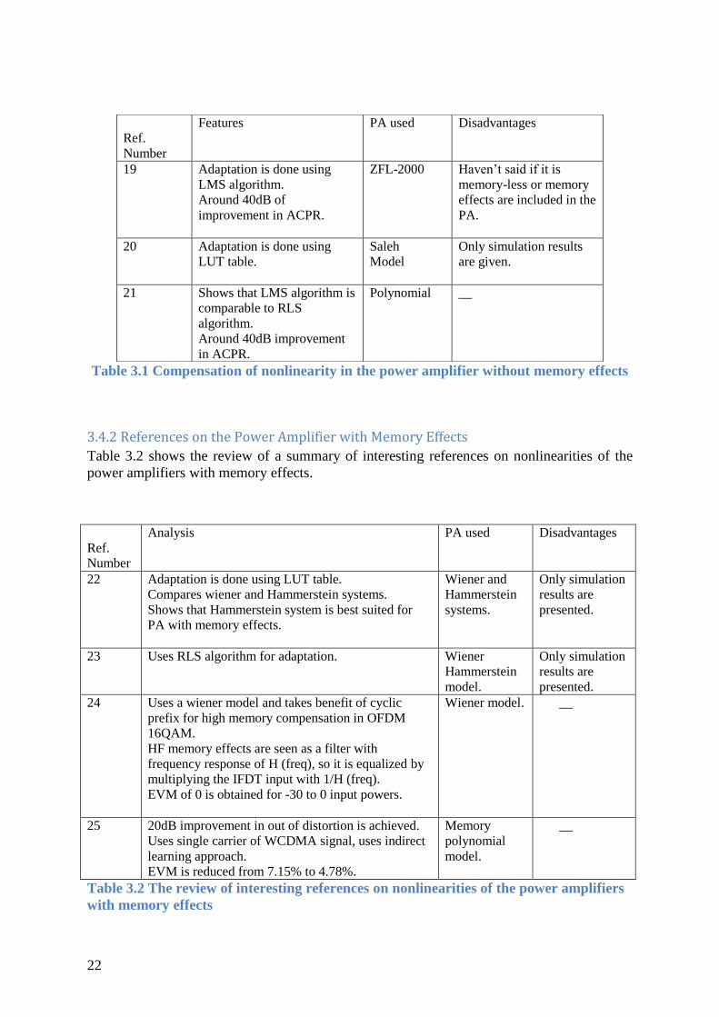
3.4.2 References on the Power Amplifier with Memory Effects
Table 3.2 shows the review of a summary of interesting references on nonlinearities of the
power amplifiers with memory effects.
Ref.
Number
Features PA used Disadvantages
19 Adaptation is done using
LMS algorithm.
Around 40dB of
improvement in ACPR.
ZFL-2000
Haven‟t said if it is
memory-less or memory
effects are included in the
PA.
20 Adaptation is done using
LUT table.
Saleh
Model
Only simulation results
are given.
21 Shows that LMS algorithm is
comparable to RLS
algorithm.
Around 40dB improvement
in ACPR.
Polynomial __
Table 3.1 Compensation of nonlinearity in the power amplifier without memory effects
Ref.
Number
Analysis PA used Disadvantages
22 Adaptation is done using LUT table.
Compares wiener and Hammerstein systems.
Shows that Hammerstein system is best suited for
PA with memory effects.
Wiener and
Hammerstein
systems.
Only simulation
results are
presented.
23 Uses RLS algorithm for adaptation. Wiener
Hammerstein
model.
Only simulation
results are
presented.
24 Uses a wiener model and takes benefit of cyclic
prefix for high memory compensation in OFDM
16QAM.
HF memory effects are seen as a filter with
frequency response of H (freq), so it is equalized by
multiplying the IFDT input with 1/H (freq).
EVM of 0 is obtained for -30 to 0 input powers.
Wiener model. __
25 20dB improvement in out of distortion is achieved.
Uses single carrier of WCDMA signal, uses indirect
learning approach.
EVM is reduced from 7.15% to 4.78%.
Memory
polynomial
model.
__
Table 3.2 The review of interesting references on nonlinearities of the power amplifiers
with memory effects

23
3.4.3 References on In-phase/Quadrature,Local Oscillator Leakage, modulator and
demodulator errors in the Transmitter and Receiver
Several techniques for IQ imbalance and dc-offset estimation and their compensation for
transmitter and receiver systems are listed.
Table 3.3 shows a summary review of interesting references on In-phase/Quadrature
imbalances and LO leakages in the TX and RX.
Ref.
Number
Analysis Blind
adaptation
( Y/N)
TX/Rx Disadvantages
26 Compensation by using digital
Intermediate Frequency (IF).
ISR of 60-100 dB is achievable.
Needs no special training or
calibration of signal.
Y TX Dc-offset aren‟t
considered.
27 Shows that time domain
compensation method is better
than Freq domain for Zero-IF.
An image suppression ratio
(ISR) of 60-100 dB is
achievable.
Y RX
28 The paper proves that frequency
selective components are within
the IQ-branches and
compensation of mean values is
sufficient to obtain good signal.
This model is valid for both
direct and low-IF.
_ RX Only simulation results
are presented.
29 This method results in overall
lower training overhead and a
lower computational
requirement. This is training
based technique.
_ TX and RX DC offset errors are not
included.
30 Gain and phase imbalance of
0.1dB and 0.1° is achieved for
zero-IF Rx. To get LO leakage
of 1dB, the measurement time
has to be increased by order of
2 in magnitude. Uses RLS
algorithm for adaptation.
_ RX
31 Shows that sample based
evaluation for I/Q imbalances
produces image rejection of 20-
40dB than mean based
evaluation for Low-IF Rx.
Y RX __
Table 3.3 the review of interesting references on In-phase / Quadrature imbalances and
LO leakages in the TX and RX.

24
3.4.4 References on joint compensation of the Power Amplifier Nonlinearity, the
Quadrature Modulator and Demodulator Errors
Only a few authors have considered the PA nonlinearities and I/Q imbalances together in
transmitter. Table 3.4 shows the review of interesting references on the PA NL, I/Q
imbalances, LO leakages in the TX and RX.
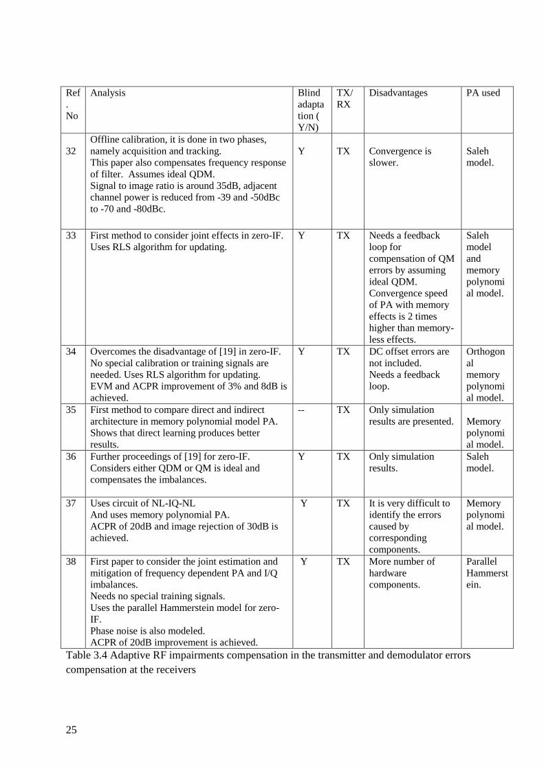
25
Ref
.
No
Analysis Blind
adapta
tion (
Y/N)
TX/
RX
Disadvantages PA used
32
Offline calibration, it is done in two phases,
namely acquisition and tracking.
This paper also compensates frequency response
of filter. Assumes ideal QDM.
Signal to image ratio is around 35dB, adjacent
channel power is reduced from -39 and -50dBc
to -70 and -80dBc.
Y
TX
Convergence is
slower.
Saleh
model.
33 First method to consider joint effects in zero-IF.
Uses RLS algorithm for updating.
Y TX Needs a feedback
loop for
compensation of QM
errors by assuming
ideal QDM.
Convergence speed
of PA with memory
effects is 2 times
higher than memory-
less effects.
Saleh
model
and
memory
polynomi
al model.
34 Overcomes the disadvantage of [19] in zero-IF.
No special calibration or training signals are
needed. Uses RLS algorithm for updating.
EVM and ACPR improvement of 3% and 8dB is
achieved.
Y TX DC offset errors are
not included.
Needs a feedback
loop.
Orthogon
al
memory
polynomi
al model.
35 First method to compare direct and indirect
architecture in memory polynomial model PA.
Shows that direct learning produces better
results.
-- TX Only simulation
results are presented.
Memory
polynomi
al model.
36 Further proceedings of [19] for zero-IF.
Considers either QDM or QM is ideal and
compensates the imbalances.
Y TX Only simulation
results.
Saleh
model.
37 Uses circuit of NL-IQ-NL
And uses memory polynomial PA.
ACPR of 20dB and image rejection of 30dB is
achieved.
Y TX It is very difficult to
identify the errors
caused by
corresponding
components.
Memory
polynomi
al model.
38 First paper to consider the joint estimation and
mitigation of frequency dependent PA and I/Q
imbalances.
Needs no special training signals.
Uses the parallel Hammerstein model for zero-
IF.
Phase noise is also modeled.
ACPR of 20dB improvement is achieved.
Y TX More number of
hardware
components.
Parallel
Hammerst
ein.
Table 3.4 Adaptive RF impairments compensation in the transmitter and demodulator errors
compensation at the receivers

26
CHAPTER 4: SIMULATION OF the DIGITAL PREDISTORTER
As far as authors best knowledge only a few references have been found that have developed
an adaptive algorithm for compensating the RF impairments using the digital predistortion
technique in the transceivers. The purpose of this chapter is to study the RF impairments in
transceiver based on references [25, 32 and 35] and a simulation chain is developed.
I have developed a simulation chain for compensation of the RF impairments (based on the
idea on the references [25, 32 and 35]). Which are done in 3 models:
Model 1: the power amplifier nonlinearities are compensated adaptively (Quadrature
modulator and demodulator are considered ideal [25]).
Model 2: compensation of nonlinearities in the power amplifiers and modulator errors are
corrected (assuming ideal demodulator [32]).
Model 3: compensation of nonlinearities in the power amplifiers and demodulator errors are
corrected (assuming ideal modulator [35]).
4.1 Simulation Chain Model 1: Compensation of nonlinearities of a power amplifier assuming ideal quadrature
modulator, quadrature demodulator and quantization noise. For the adaptive digital
predistortion we use an indirect learning architecture which is shown in Figure 4.1.
Figure 4.1 Adaptive PD for compensation of the power amplifier nonlinearity
Working Procedure: Here the PD training(post distorter) uses the output of the power
amplifier to find the input of the power amplifier, it means that the PD training is used to find
the inverse transfer function of the power amplifier so that when cascaded together the output
will be constant.
Here, PD is the replica of the PD training i.e after finding the coefficinets from post distorter
this values are copied at PD. For adaptation we use normalized least mean square algorithm
(NLMS).
In the Figure 4.1 s(n) represents the input signal and n corresponds to samples, G represents
gain of the power amplifier.
27
Assuming both the predistorter and power amplifier as memory polynomial model, the output
of post-distorter is
𝑧 𝑛 = akq
𝑄−1
𝑞=0
𝐾−1𝑘=1
𝑦 𝑛−𝑞
𝐺
|𝑦 𝑛−𝑞 |𝑘−1
𝐺𝐾−1, (4.1)
Here K is polynomial coefficinet, Q is memory depth, and G is gain of the power amplifier.
Here z (n) designates an estimate of actual input x(n), we collect the parameters akq
Into J*1 vector, say A, where J is the total number of parameters. It can be expressed as
A = [a1,0 … . . aK,0 …… a1,Q …… . aKQ ]^T. (4.2)
let 𝑈𝑘 ,𝑞 𝑛 =𝑦 𝑛−𝑞
𝐺
|𝑦 𝑛−𝑞 |𝑘−1
𝐺𝐾−1 . (4.3)
(4.3) can be written in matrix form as follows
z = UB, (4.4)
Here z 𝑛 = 𝑧 0 ,…………𝑧 𝑁 − 1 𝑇 .
U = [u1,0 … . . uK,0 ……u1,Q …… . uKQ ]
uk,q = [uk,q(0)… . . uk,q (N − 1)]^T
The size of Z and U is N*1 and N*J, respectively, as in the Figure 4.1, error can be written
as 𝑒 𝑛 = 𝑥 𝑛 − 𝑧(𝑛).
Since z(n) is linear in the parameterakq , A can be find out using LMS algorithm
i.e.,w (n+1) = w(n) + mu * conj(error)*U. (4.5)
Assumptions: initally the co-efficinets of PD and PD training are taken according to the ideal
power amplifier,
i.e., akq = 0 for q! = 0
a10 = 1 (ideal PA)
ak0 = 0 for k! =0
Here a, k and q corresponds to coefficient of the memory polynomial model, polynomial
order and memory depth.
Let a = 5 and q = 2, so we have nine co-efficient of PD and PD training blocks. Assuming
initial value of weights is zero except the first weight which is unity.
i.e., akq = [1, 0, 0 ………].
Gain error = 0.3, phase error = 10° and dc-offset = 0.05 + j0.05.
Results
28
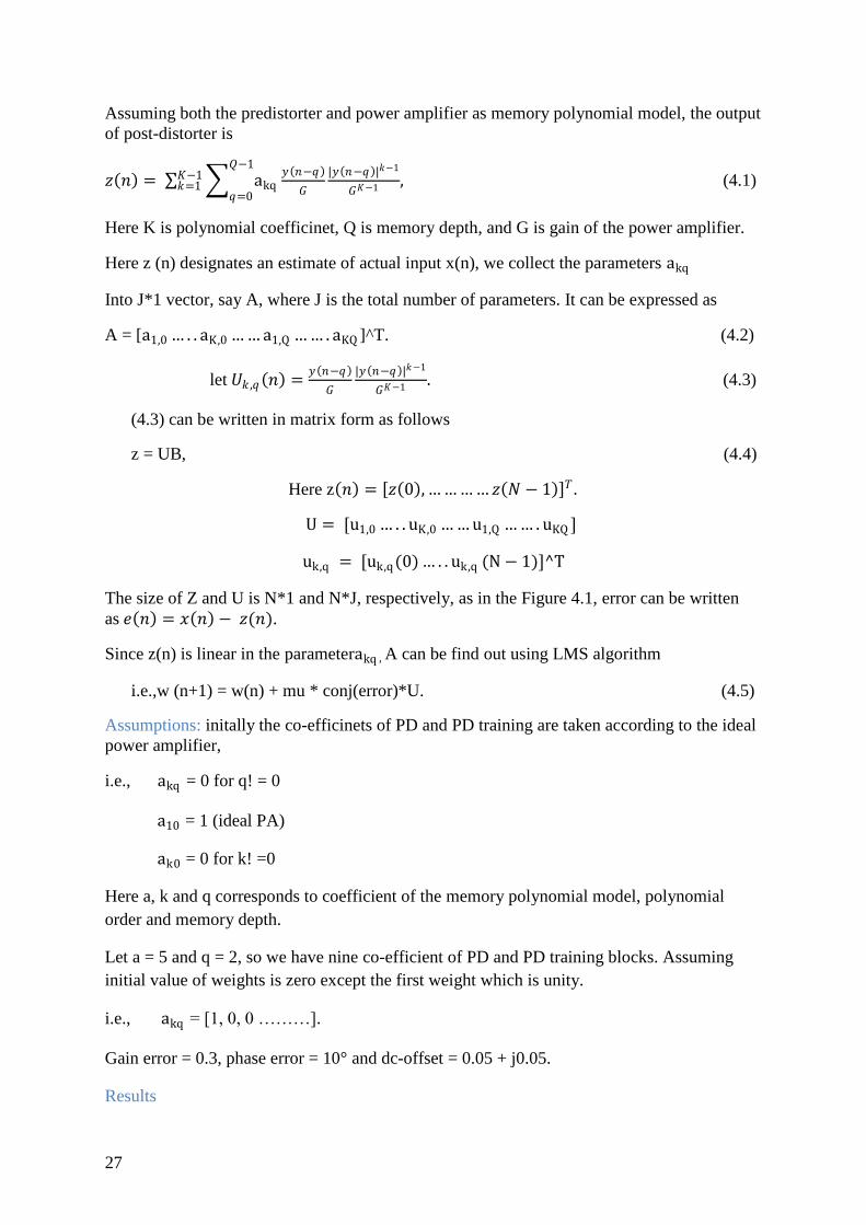
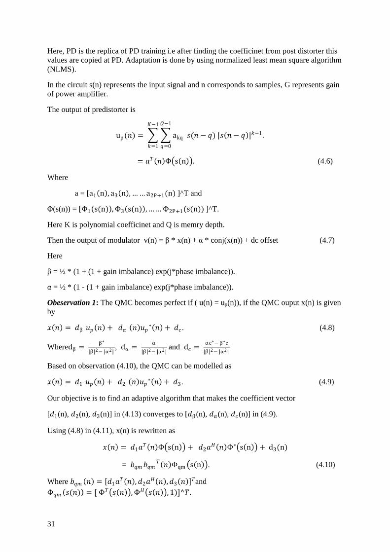
The following results when both the PD and PA is memory polynomial model,
AM/AM curves before and after compensation are shown in Figure 4.2, here red color graph
is before compensation and blue curve is after compensation.
Figure 4.2 AM/AM curves (ideal QM and QDM)
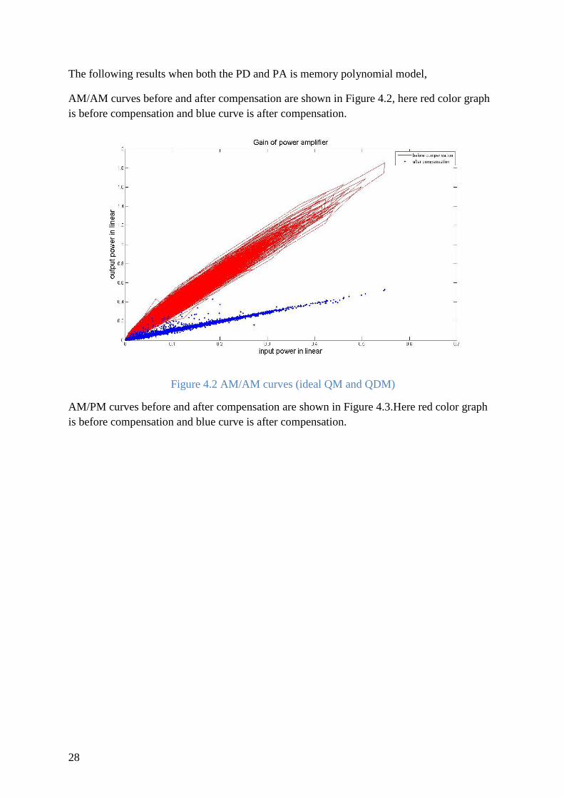
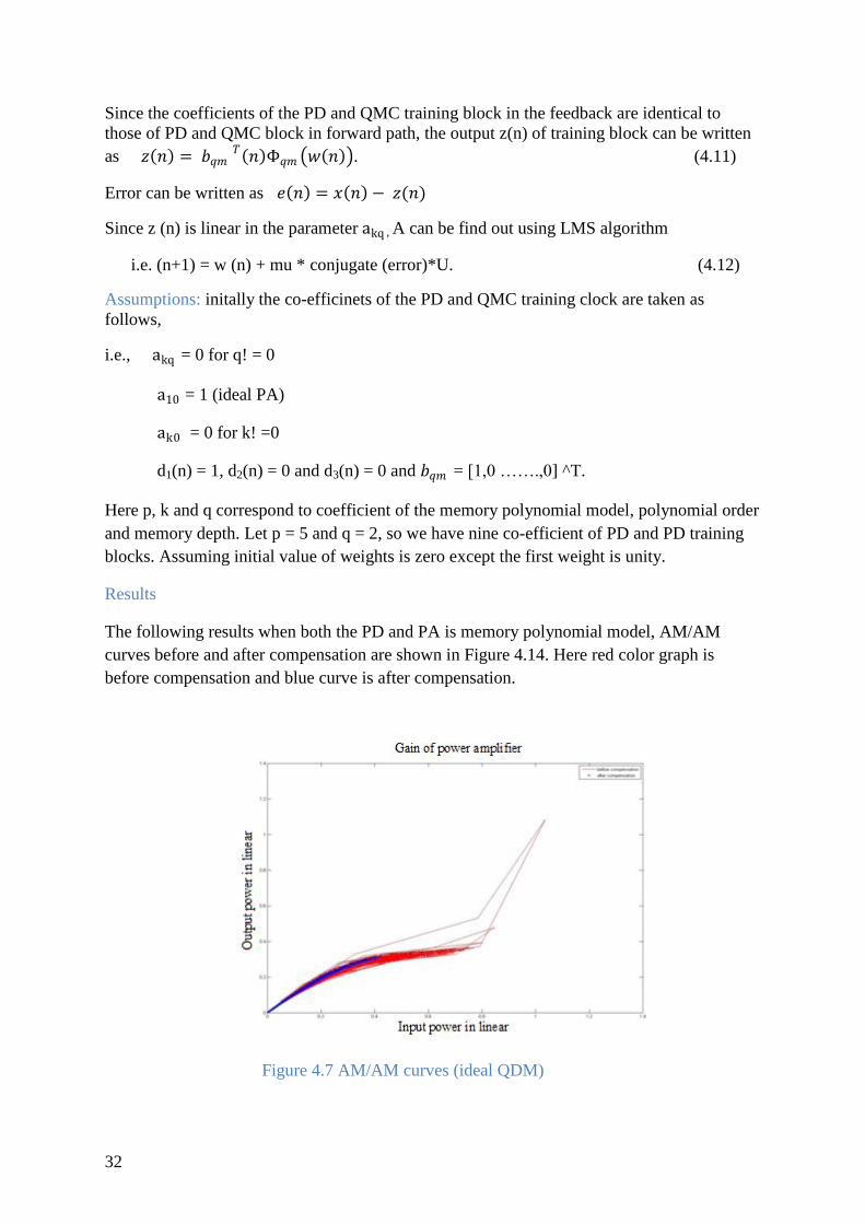
AM/PM curves before and after compensation are shown in Figure 4.3.Here red color graph
is before compensation and blue curve is after compensation.
29
Figure 4.3 AMPM curves (Ideal QM and QDM)
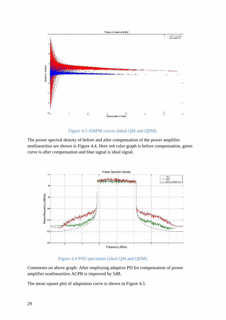
The power spectral density of before and after compensation of the power amplifier
nonlinearities are shown in Figure 4.4. Here red color graph is before compensation, green
curve is after compensation and blue signal is ideal signal.
Figure 4.4 PSD spectrums (ideal QM and QDM)
Comments on above graph: After employing adaptive PD for compensation of power
amplifier nonlinearities ACPR is improved by 5dB.
The mean square plot of adaptation curve is shown in Figure 4.5.
30
Figure 4.5 MSE curve for ideal QM and QDM
Table 4.1 shows EVM with/without adaptive DPD.
S. NO EVM in dB without DPD EVM in dB with adaptive DPD
1 8.622 0.34
Table 4.1 EVM with and without DPD
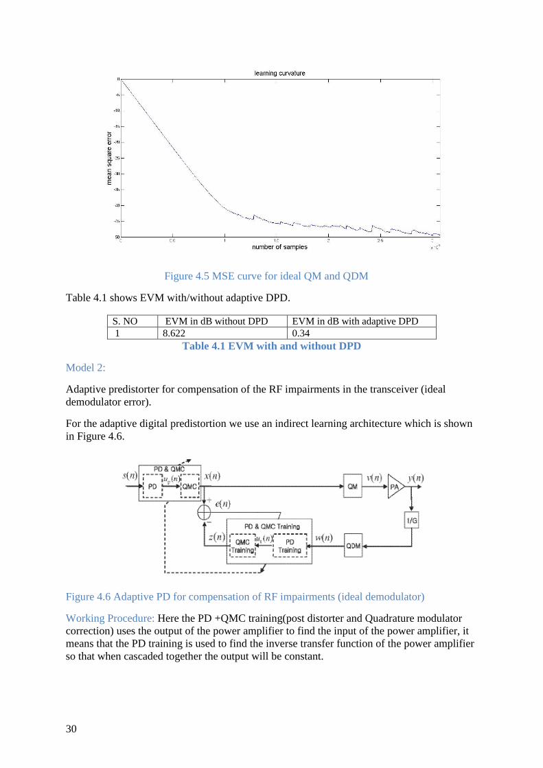
Model 2:
Adaptive predistorter for compensation of the RF impairments in the transceiver (ideal
demodulator error).
For the adaptive digital predistortion we use an indirect learning architecture which is shown
in Figure 4.6.
Figure 4.6 Adaptive PD for compensation of RF impairments (ideal demodulator)
Working Procedure: Here the PD +QMC training(post distorter and Quadrature modulator
correction) uses the output of the power amplifier to find the input of the power amplifier, it
means that the PD training is used to find the inverse transfer function of the power amplifier
so that when cascaded together the output will be constant.
31
Here, PD is the replica of PD training i.e after finding the coefficinet from post distorter this
values are copied at PD. Adaptation is done by using normalized least mean square algorithm
(NLMS).
In the circuit s(n) represents the input signal and n corresponds to samples, G represents gain
of power amplifier.
The output of predistorter is
up (𝑛) = akq
𝑄−1
𝑞=0
𝐾−1
𝑘=1
𝑠(𝑛 − 𝑞) |𝑠 𝑛 − 𝑞 |𝑘−1.
= 𝑎𝑇 𝑛 Φ s n . (4.6)
Where
a = [a1 n , a3 n ,…… a2P+1(n) ]^T and
Φ(s(n)) = [Φ1 s(n) ,Φ3 s(n) ,……Φ2P+1(s(n)) ]^T.
Here K is polynomial coefficinet and Q is memry depth.
Then the output of modulator v(n) = β * x(n) + α * conj(x(n)) + dc offset (4.7)
Here
β = ½ * (1 + (1 + gain imbalance) exp(j*phase imbalance)).
α = ½ * (1 - (1 + gain imbalance) exp(j*phase imbalance)).
Obeservation 1: The QMC becomes perfect if ( u(n) = up(n)), if the QMC ouput x(n) is given
by
𝑥 𝑛 = 𝑑β 𝑢𝑝 𝑛 + 𝑑α 𝑛 𝑢𝑝∗ 𝑛 + 𝑑𝑐 . (4.8)
Wheredβ = β∗
|β|2− |α2| , dα =
α
|β|2− |α2| and dc =
αc∗− β∗c
|β|2− |α2|
Based on observation (4.10), the QMC can be modelled as
𝑥 𝑛 = 𝑑1 𝑢𝑝 𝑛 + 𝑑2 𝑛 𝑢𝑝∗ 𝑛 + 𝑑3. (4.9)
Our objective is to find an adaptive algorithm that makes the coefficient vector
[𝑑1(n), 𝑑2(n), 𝑑3(n)] in (4.13) converges to [𝑑β(n), 𝑑α (n), 𝑑𝑐(n)] in (4.9).
Using (4.8) in (4.11), x(n) is rewritten as
𝑥 𝑛 = 𝑑1𝑎𝑇 𝑛 Φ s n + 𝑑2𝑎
𝐻 𝑛 Φ∗ s n + d3(n)
= 𝑏𝑞𝑚𝑏𝑞𝑚𝑇 𝑛 Φqm s n . (4.10)
Where 𝑏𝑞𝑚 𝑛 = 𝑑1𝑎𝑇 𝑛 ,𝑑2𝑎
𝐻 𝑛 ,𝑑3 𝑛 𝑇and
Φ𝑞𝑚 𝑠(𝑛) = [ Φ𝑇 𝑠 𝑛 ,Φ𝐻 𝑠 𝑛 , 1)]^𝑇.
32
Since the coefficients of the PD and QMC training block in the feedback are identical to
those of PD and QMC block in forward path, the output z(n) of training block can be written
as 𝑧 𝑛 = 𝑏𝑞𝑚 𝑇 𝑛 Φ𝑞𝑚 𝑤 𝑛 . (4.11)
Error can be written as 𝑒 𝑛 = 𝑥 𝑛 − 𝑧(𝑛)
Since z (n) is linear in the parameter akq , A can be find out using LMS algorithm
i.e. (n+1) = w (n) + mu * conjugate (error)*U. (4.12)
Assumptions: initally the co-efficinets of the PD and QMC training clock are taken as
follows,
i.e., akq = 0 for q! = 0
a10 = 1 (ideal PA)
ak0 = 0 for k! =0
d1(n) = 1, d2(n) = 0 and d3(n) = 0 and 𝑏𝑞𝑚 = [1,0 …….,0] ^T.
Here p, k and q correspond to coefficient of the memory polynomial model, polynomial order
and memory depth. Let p = 5 and q = 2, so we have nine co-efficient of PD and PD training
blocks. Assuming initial value of weights is zero except the first weight is unity.
Results
The following results when both the PD and PA is memory polynomial model, AM/AM
curves before and after compensation are shown in Figure 4.14. Here red color graph is
before compensation and blue curve is after compensation.
Figure 4.7 AM/AM curves (ideal QDM)
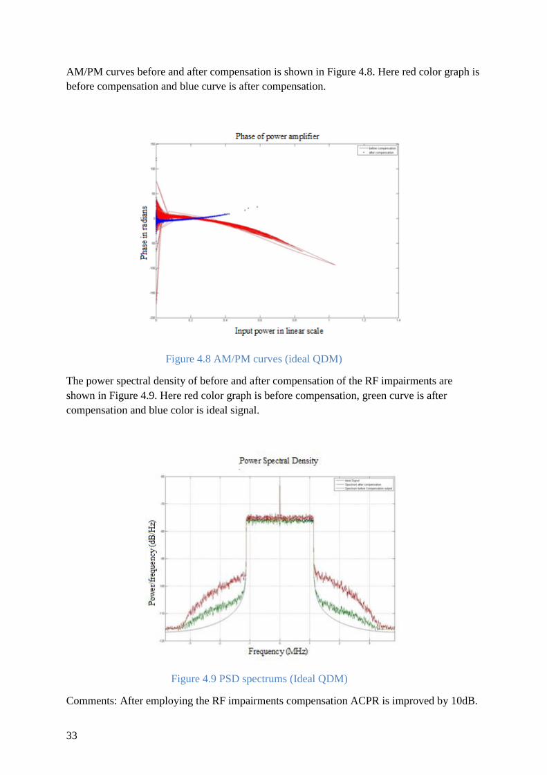
33
AM/PM curves before and after compensation is shown in Figure 4.8. Here red color graph is
before compensation and blue curve is after compensation.
Figure 4.8 AM/PM curves (ideal QDM)
The power spectral density of before and after compensation of the RF impairments are
shown in Figure 4.9. Here red color graph is before compensation, green curve is after
compensation and blue color is ideal signal.
Figure 4.9 PSD spectrums (Ideal QDM)
Comments: After employing the RF impairments compensation ACPR is improved by 10dB.
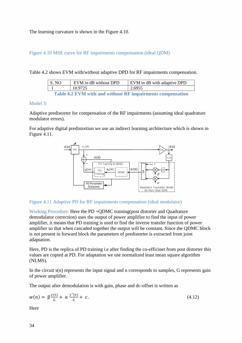
34
The learning curvature is shown in the Figure 4.10.
Figure 4.10 MSE curve for RF impairments compensation (ideal QDM)
Table 4.2 shows EVM with/without adaptive DPD for RF impairments compensation.
S. NO EVM in dB without DPD EVM in dB with adaptive DPD
1 10.9725 2.6955
Table 4.2 EVM with and without RF impairments compensation
Model 3:
Adaptive predistorter for compensation of the RF impairments (assuming ideal quadrature
modulator errors).
For adaptive digital predistortion we use an indirect learning architecture which is shown in
Figure 4.11.
Figure 4.11 Adaptive PD for RF impairments compensation (ideal modulator)
Working Procedure: Here the PD +QDMC training(post distorter and Quadrature
demodulator correction) uses the output of power amplifier to find the input of power
amplifier, it means that PD training is used to find the inverse transfer function of power
amplifier so that when cascaded together the output will be constant. Since the QDMC block
is not present in forward block the parameters of predistorter is extracted from joint
adaptation.
Here, PD is the replica of PD training i.e after finding the co-efficinet from post distorter this
values are copied at PD. For adaptation we use normalized least mean square algorithm
(NLMS).
In the circuit s(n) represents the input signal and n corresponds to samples, G represents gain
of power amplifier.
The output after demodulation is with gain, phase and dc-offset is written as
𝑤 𝑛 = βy(n)
G+ α
y∗(n)
G+ c . (4.12)
Here
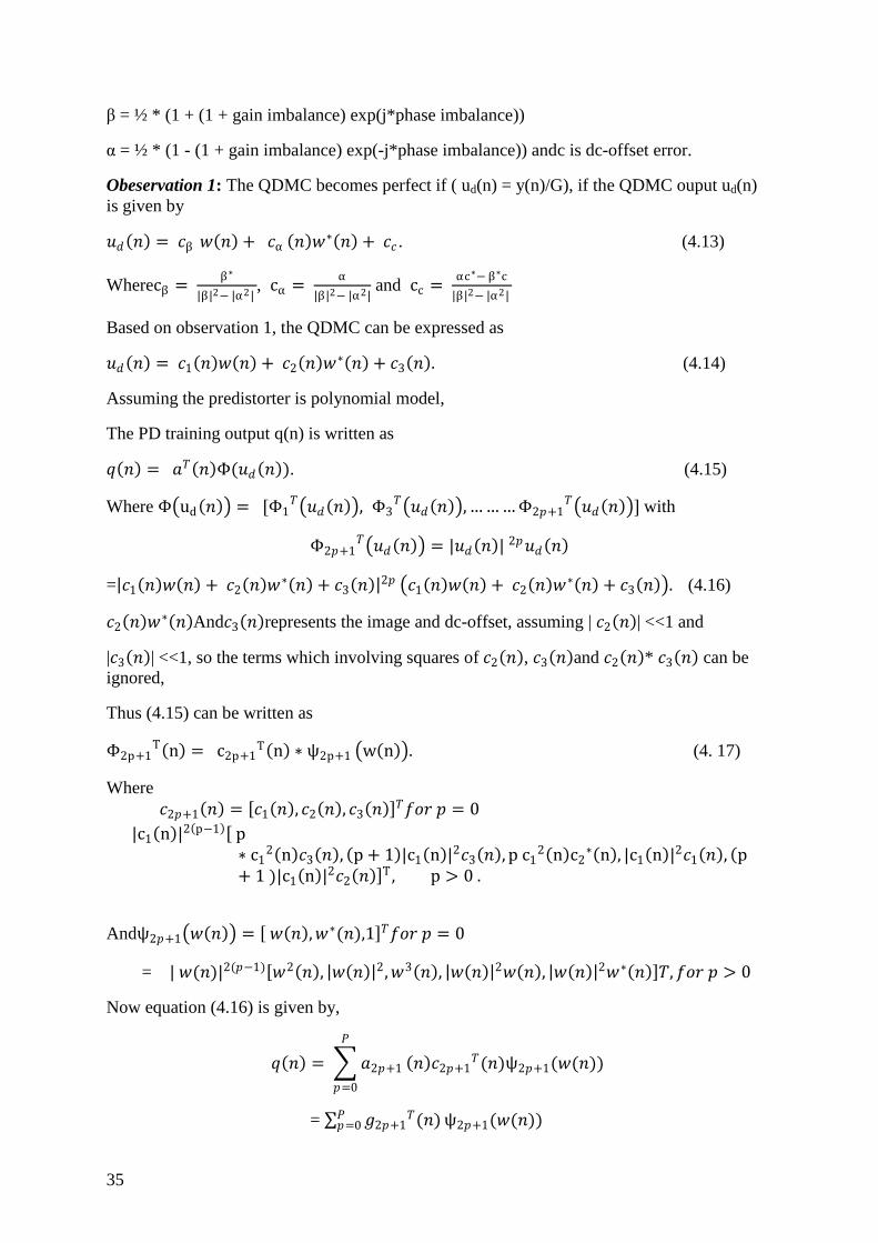
35
β = ½ * (1 + (1 + gain imbalance) exp(j*phase imbalance))
α = ½ * (1 - (1 + gain imbalance) exp(-j*phase imbalance)) andc is dc-offset error.
Obeservation 1: The QDMC becomes perfect if ( ud(n) = y(n)/G), if the QDMC ouput ud(n)
is given by
𝑢𝑑 𝑛 = 𝑐β 𝑤 𝑛 + 𝑐α 𝑛 𝑤∗ 𝑛 + 𝑐𝑐 . (4.13)
Wherecβ = β∗
|β|2− |α2| , cα =
α
|β|2− |α2| and cc =
αc∗− β∗c
|β|2− |α2|
Based on observation 1, the QDMC can be expressed as
𝑢𝑑 𝑛 = 𝑐1 𝑛 𝑤 𝑛 + 𝑐2 𝑛 𝑤∗ 𝑛 + 𝑐3 𝑛 . (4.14)
Assuming the predistorter is polynomial model,
The PD training output q(n) is written as
𝑞 𝑛 = 𝑎𝑇 𝑛 Φ(𝑢𝑑 𝑛 ). (4.15)
Where Φ ud 𝑛 = [Φ1𝑇 𝑢𝑑 𝑛 , Φ3
𝑇 𝑢𝑑 𝑛 ,………Φ2𝑝+1𝑇 𝑢𝑑 𝑛 ] with
Φ2𝑝+1𝑇 𝑢𝑑 𝑛 = |𝑢𝑑 𝑛 | 2𝑝𝑢𝑑 𝑛
= 𝑐1 𝑛 𝑤 𝑛 + 𝑐2 𝑛 𝑤∗ 𝑛 + 𝑐3 𝑛
2𝑝 𝑐1 𝑛 𝑤 𝑛 + 𝑐2 𝑛 𝑤∗ 𝑛 + 𝑐3 𝑛 . (4.16)
𝑐2 𝑛 𝑤∗ 𝑛 And𝑐3 𝑛 represents the image and dc-offset, assuming | 𝑐2 𝑛 | <<1 and
|𝑐3 𝑛 | <<1, so the terms which involving squares of 𝑐2 𝑛 , 𝑐3 𝑛 and 𝑐2 𝑛 * 𝑐3 𝑛 can be
ignored,
Thus (4.15) can be written as
Φ2p+1T n = c2p+1
T n ∗ ψ2p+1 w n . (4. 17)
Where
𝑐2𝑝+1 𝑛 = 𝑐1 𝑛 , 𝑐2 𝑛 , 𝑐3 𝑛 𝑇𝑓𝑜𝑟 𝑝 = 0
|c1 n |2 p−1 p∗ c1
2 n 𝑐3 𝑛 , p + 1 |c1 n |2𝑐3 𝑛 , p c12 n c2
∗ n , |c1 n |2𝑐1 𝑛 , p+ 1 |c1 n |2𝑐2 𝑛
T , p > 0 .
Andψ2𝑝+1 𝑤 𝑛 = 𝑤 𝑛 ,𝑤∗(𝑛),1 𝑇𝑓𝑜𝑟 𝑝 = 0
= | 𝑤(𝑛)|2(𝑝−1) 𝑤2 𝑛 , 𝑤 𝑛 2,𝑤3 𝑛 , 𝑤 𝑛 2𝑤 𝑛 , 𝑤 𝑛 2𝑤∗ 𝑛 𝑇,𝑓𝑜𝑟 𝑝 > 0
Now equation (4.16) is given by,
𝑞 𝑛 = 𝑎2𝑝+1
𝑃
𝑝=0
𝑛 𝑐2𝑝+1𝑇(𝑛)ψ2𝑝+1(𝑤(𝑛))
= 𝑔2𝑝+1𝑇(𝑛)𝑃
𝑝=0 ψ2𝑝+1(𝑤(𝑛))

36
= 𝑏𝑞𝑑𝑚 𝑛 ∗ ψ 𝑤 𝑛 . (4.18)
Where 𝑔2𝑝+1 𝑛 = 𝑎2𝑝+1 𝑛 𝑐2𝑝+1 𝑛 , 𝑏𝑞𝑑𝑚 𝑛 = [𝑔1𝑇 𝑛 , 𝑔2
𝑇 𝑛 ,…𝑔2𝑝+1𝑇 𝑛 ]^𝑇
ψ𝑞𝑑𝑚 𝑤 𝑛 = ψ1𝑇 𝑤 𝑛 , . . . . .ψ2𝑝+1
𝑇 𝑤 𝑛 .
Equation (4.17) represents the polynomial for joint QDMC and PD.
The parameters of the predistorter are extracted from the equation (4.18),
The values of c1(n), c2(n) and c3(n) in the equation (4.18) are given by 𝑐1 𝑛 = 1− γ∗ 𝑛
(1−|γ n |)2
𝑐2 𝑛 =γ n −|γ n |2
(1−|γ n |)2 , where γ n = g1
2(n)
g11(n)
.
Similarly it can be seen from the definitions of 𝑔2𝑝+1(𝑛) and 𝑐2𝑝+1(𝑛) that
𝑎2𝑝+1 = g1
1 n + g12(n)
𝑐1 𝑛 + 𝑐2 𝑛 for p = 0
= g2p+1
4 n + g2p+15(n)
|𝑐1 𝑛 |2p(𝑐1 𝑛 + (𝑝 + 1)𝑐2 𝑛 ) for p > 0.
As in the Figure 4.11 error signal can be written as
𝑒 𝑛 = 𝑢𝑝 𝑛 − 𝑞(𝑛)
Since z (n) is linear in the parameter akq , A can be find out using LMS algorithm
i.e., w (n+1) = w(n) + mu * conj(error)*U.
Assumptions: initally the co-efficinets of the PD and PD training corresponding to the ideal
power amplifier,
i.e., akq = 0 for q! = 0
a10 = 1 (ideal PA)
ak0 = 0 for k! =0
𝑐1 𝑛 = 1, 𝑐2 𝑛 = 0 and 𝑐3 𝑛 = 0 and 𝑏𝑞𝑑𝑚 = 1, 0,…… ,0 𝑇 .
Here a, k and q corresponds to coefficient of the memory polynomial model, polynomial
order and memory depth. Let a = 4, so we have 4 co-efficient for PD and PD training blocks.
Assuming initial value of weights is zero expect the first weight is 1.
Results: The following results when both the PD is polynomial and PA is Saleh model.
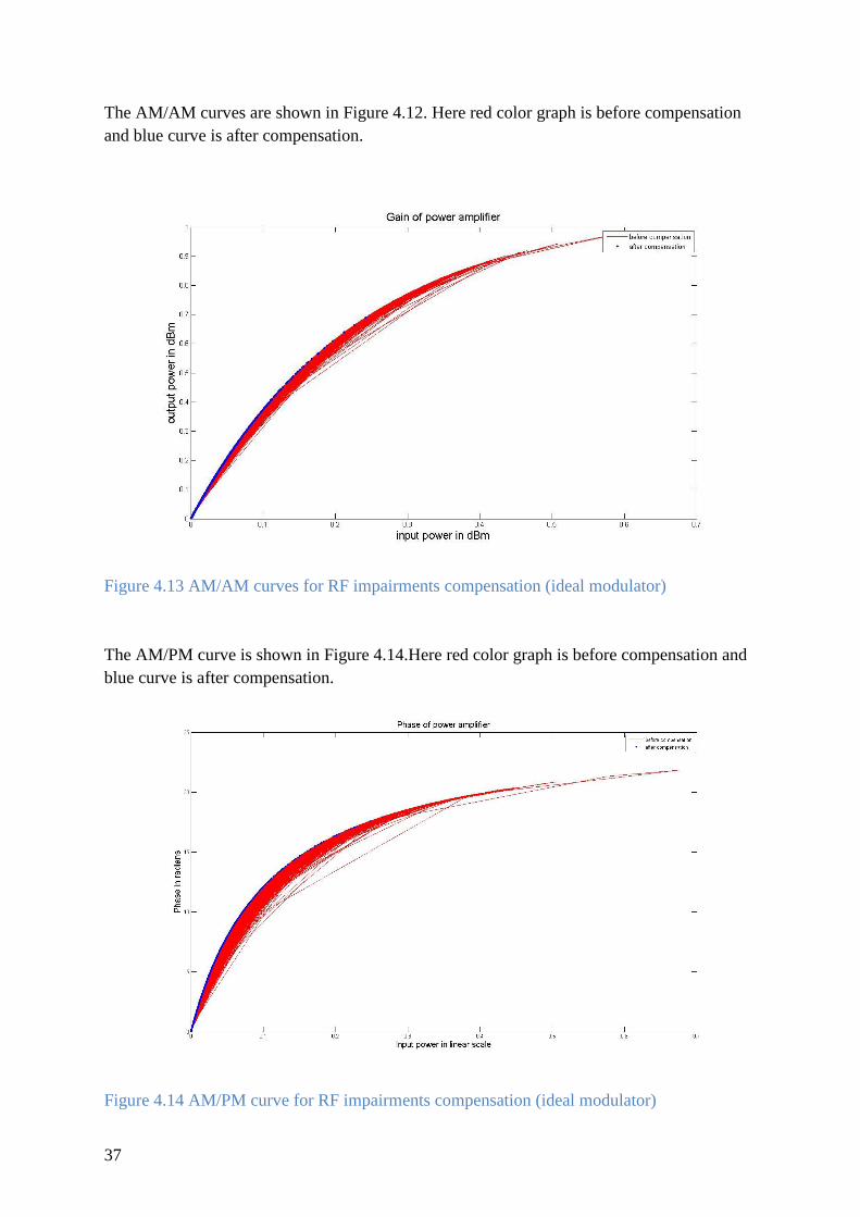
37
The AM/AM curves are shown in Figure 4.12. Here red color graph is before compensation
and blue curve is after compensation.
Figure 4.13 AM/AM curves for RF impairments compensation (ideal modulator)
The AM/PM curve is shown in Figure 4.14.Here red color graph is before compensation and
blue curve is after compensation.
Figure 4.14 AM/PM curve for RF impairments compensation (ideal modulator)
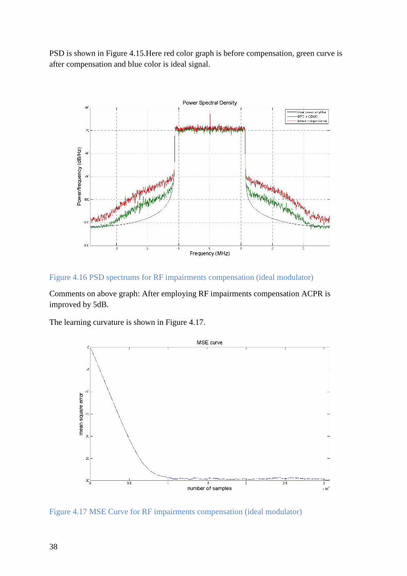
38
PSD is shown in Figure 4.15.Here red color graph is before compensation, green curve is
after compensation and blue color is ideal signal.
Figure 4.16 PSD spectrums for RF impairments compensation (ideal modulator)
Comments on above graph: After employing RF impairments compensation ACPR is
improved by 5dB.
The learning curvature is shown in Figure 4.17.
Figure 4.17 MSE Curve for RF impairments compensation (ideal modulator)

39
Table 4.3shows EVM with/without adaptive DPD for RF impairments compensation
S. NO EVM in dB without DPD EVM in dB with adaptive DPD
1 8.1 0.84
Table 4.3 EVM with and without RF impairments compensation (ideal modulator)

40
Chapter 5: IMPLEMENTATIONOF ADAPTIVEDIGITAL
PREDISTORTIONFOR RADIO FREQUENCY IMPAIRMENTS
COMPENSATION IN ACTUAL SYSTEMS.
5.1Modeling
Signal used is LTE of BW 5MHz.
Architecture used in thesis: In the Thesis work Lime LMS 6002D chip wasn’t used as
the work was optional. So, in the Thesis work, algorithm is developed in Matlab
software by assuming the LMS 6002D architecture.
This chip covers up to 0.3-3.8GHz frequency range in transceivers, especially used for femto cell and pico cell base stations and also in broad band wireless communication devices for WCDMA/HSPA, LTE, CDMA, IEEE 802.16x radios. More details about the chip can be found at http://www.limemicro.com/products.php.
The target of the thesis is to obtain 3dB increase in Transmission power.
Plotting the LTE signal in frequency domain is shown in Figure 5.1.
Figure 5.1 LTE signal
5.2Target to Achieve Improvement in ACPR of 33dB after compensation of the RF impairments.
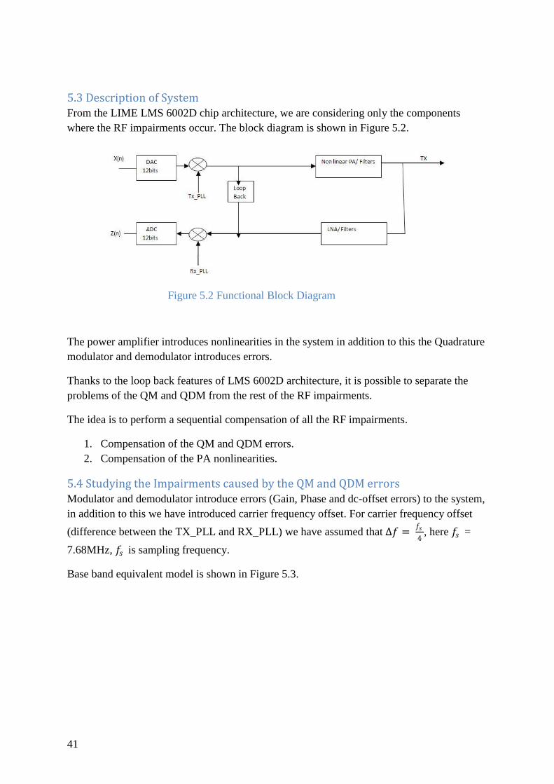
41
5.3 Description of System From the LIME LMS 6002D chip architecture, we are considering only the components
where the RF impairments occur. The block diagram is shown in Figure 5.2.
Figure 5.2 Functional Block Diagram
The power amplifier introduces nonlinearities in the system in addition to this the Quadrature
modulator and demodulator introduces errors.
Thanks to the loop back features of LMS 6002D architecture, it is possible to separate the
problems of the QM and QDM from the rest of the RF impairments.
The idea is to perform a sequential compensation of all the RF impairments.
1. Compensation of the QM and QDM errors.
2. Compensation of the PA nonlinearities.
5.4 Studying the Impairments caused by the QM and QDM errors Modulator and demodulator introduce errors (Gain, Phase and dc-offset errors) to the system,
in addition to this we have introduced carrier frequency offset. For carrier frequency offset
(difference between the TX_PLL and RX_PLL) we have assumed that ∆𝑓 = 𝑓𝑠
4, here 𝑓𝑠 =
7.68MHz, 𝑓𝑠 is sampling frequency.
Base band equivalent model is shown in Figure 5.3.

42
Figure 5.3 Baseband model
Carrier frequency offset is introduced by multiplying feedback signal with exp (2pi (1/4)n)
(blue box in the above figure). Errors at modulator and demodulator are shown in red box.
Working Procedure:
Here input signal is complex signal, let the real part signal be a cosine and the imaginary part
signal a sine signal. Let the frequency of base band signal be 100 kHz and sampling
frequency be7.68MHz.
Let x (n) be the input signal, if we want to observe the fundamental tone, as the unit of input
frequency is Hz, so for plotting in linear scale or dB scale we divide input frequency by
sampling frequency i.e.100 e3
7.68 e6 = 0.01302.In all the Figures from 5.4 to 5.9, y-axis is in dB
scale and x-axis is in linear scale.
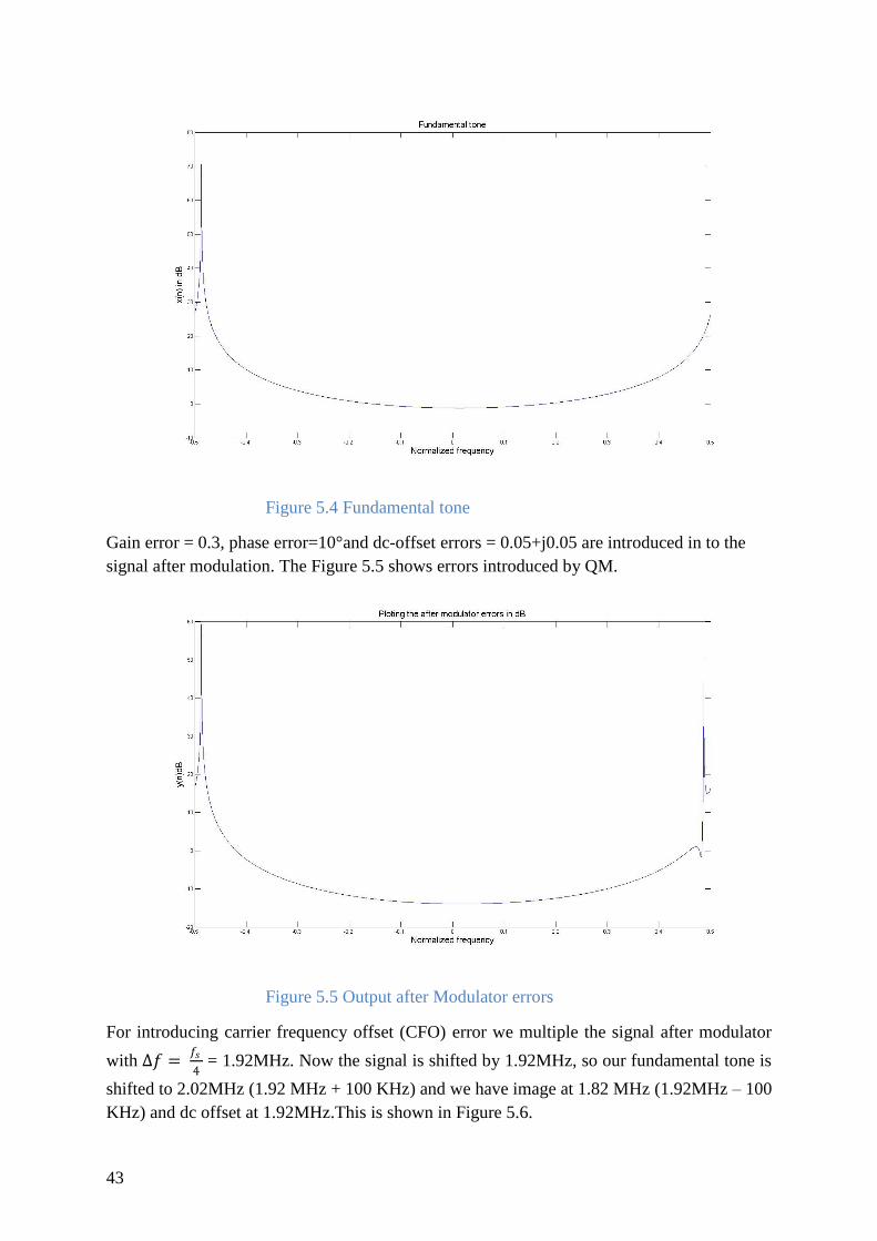
43
Figure 5.4 Fundamental tone
Gain error = 0.3, phase error=10°and dc-offset errors = 0.05+j0.05 are introduced in to the
signal after modulation. The Figure 5.5 shows errors introduced by QM.
Figure 5.5 Output after Modulator errors
For introducing carrier frequency offset (CFO) error we multiple the signal after modulator
with ∆𝑓 = 𝑓𝑠
4 = 1.92MHz. Now the signal is shifted by 1.92MHz, so our fundamental tone is
shifted to 2.02MHz (1.92 MHz + 100 KHz) and we have image at 1.82 MHz (1.92MHz – 100
KHz) and dc offset at 1.92MHz.This is shown in Figure 5.6.
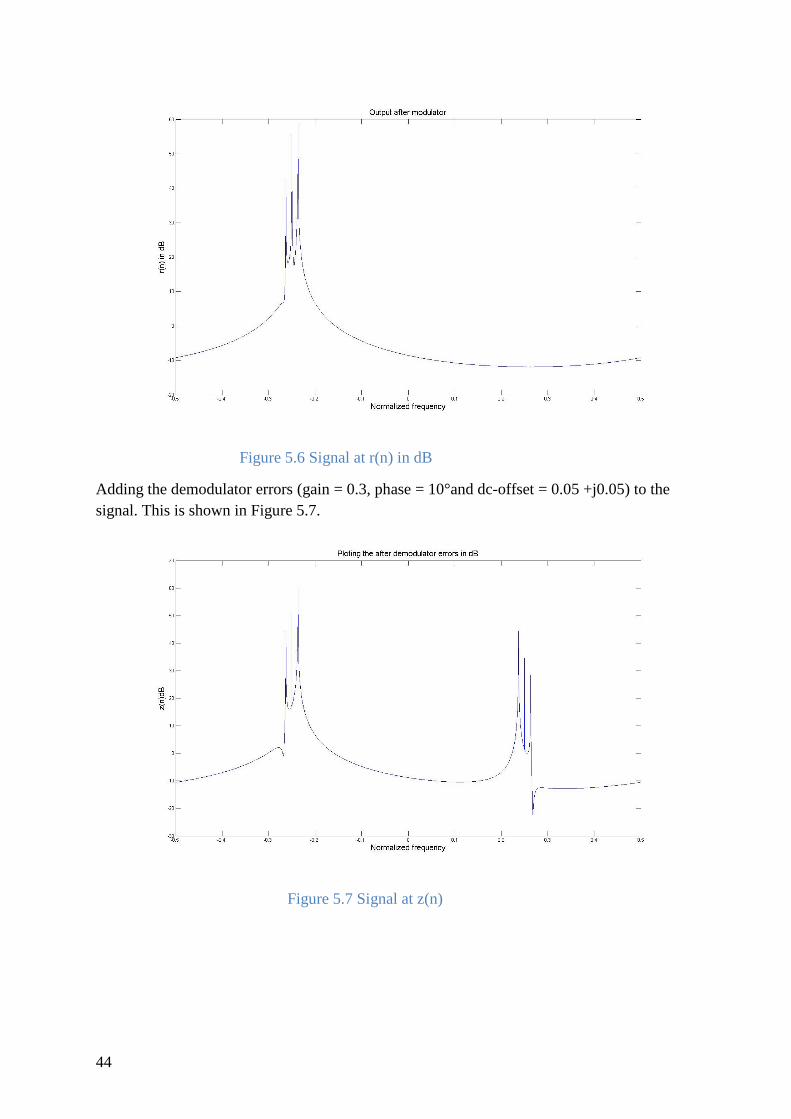
44
Figure 5.6 Signal at r(n) in dB
Adding the demodulator errors (gain = 0.3, phase = 10°and dc-offset = 0.05 +j0.05) to the
signal. This is shown in Figure 5.7.
Figure 5.7 Signal at z(n)

45
5.2.1 QM Impairment Implementation
For removing the errors caused by demodulator, we use a Hilbert filter of order 50. Here the
pass band of Hilbert filter is from 0.2 to 0.5 in an interval of 0 to 1 and rest is the stop band
(in Matlab, interval of a filter should be in a range of 0 to 1).
As the signal is shifted by multiplied by ¼ for CFO, we bring back the signal to original state
by multiplying with exp (j2pi(-1/4)n).
The block diagram of the Hilbert Signal and shifting of the signal is shown in Figure 5.8.
Figure 5.8 Hilbert filter
The signal at F (n) is shown in Figure 5.9.
Figure 5.9Signals at F (n)
5.2.2 QDM error compensation
For removing the errors caused by demodulator, we use a Hilbert filter of order 50. Here the
pass band of Hilbert filter is from 0.2 to 0.5 in an interval of 0 to 1 and rest is the stop band
(in Matlab, interval of a filter should be in a range of 0 to 1).

46
5.3 Adaptive Quadrature Modulator Error Compensation (Ideal Demodulator) If we observe in Figure 5.10 we can see observe the dc-offset and image tone. So for
compensation of image tone and dc-offset we use a component called Quadrature modulator
correction.
The block diagram of compensation of the QM errors is shown in Figure 5.10.
Figure 5.10 Adaptive QMC for compensation of modulator errors (ideal demodulator)
In the Figure 5.11 red box shows Quadrature modulator errors and blue box shows CFO.
Working procedure: The working procedure is same as 5.2 except the demodulator is ideal.
For testing the above scheme we use complex signal (cosine as real signal and sine as
imaginary signal) and later we use the LTE signal.
Operation 1:
Input signal: complex input with fundamental tone of 100 kHz,
Gain error = 0.3, Phase error = 10°and dc offset = 0.05+ 0.05j.
The Figure 5.11 shows the signal y(n) (after modulator errors).
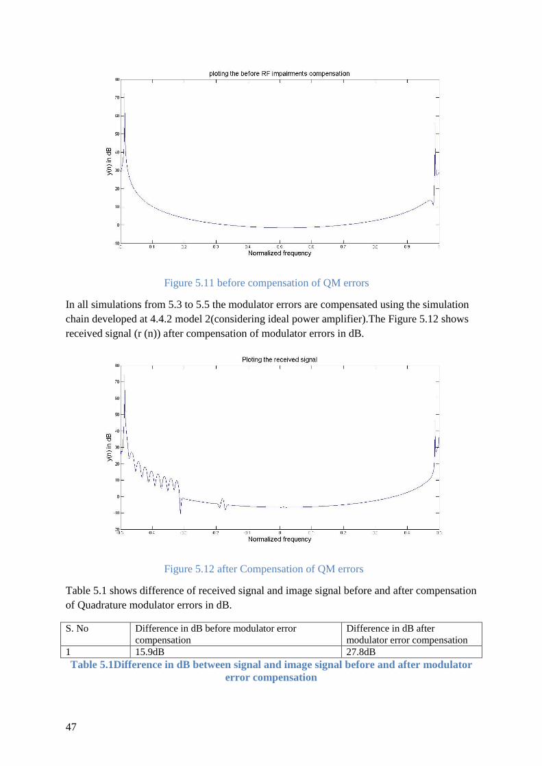
47
Figure 5.11 before compensation of QM errors
In all simulations from 5.3 to 5.5 the modulator errors are compensated using the simulation
chain developed at 4.4.2 model 2(considering ideal power amplifier).The Figure 5.12 shows
received signal (r (n)) after compensation of modulator errors in dB.
Figure 5.12 after Compensation of QM errors
Table 5.1 shows difference of received signal and image signal before and after compensation
of Quadrature modulator errors in dB.
S. No Difference in dB before modulator error
compensation
Difference in dB after
modulator error compensation
1 15.9dB 27.8dB
Table 5.1Difference in dB between signal and image signal before and after modulator
error compensation
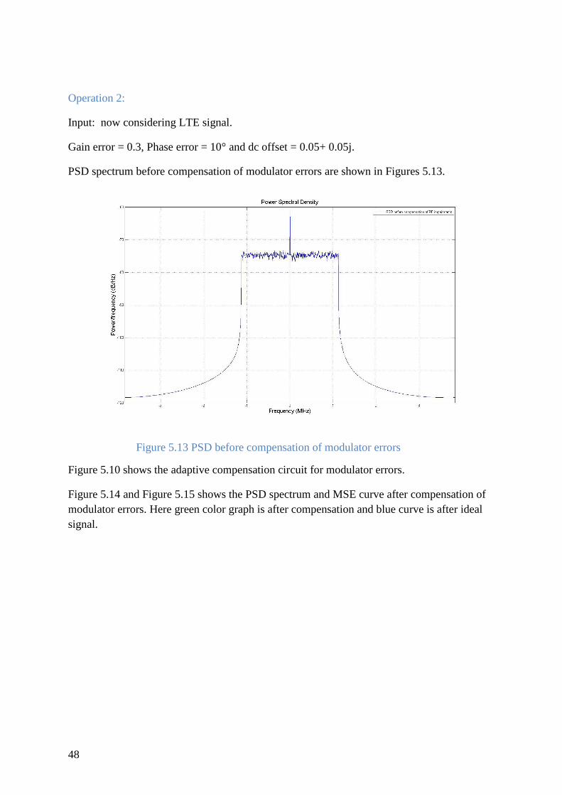
48
Operation 2:
Input: now considering LTE signal.
Gain error = 0.3, Phase error = 10° and dc offset = 0.05+ 0.05j.
PSD spectrum before compensation of modulator errors are shown in Figures 5.13.
Figure 5.13 PSD before compensation of modulator errors
Figure 5.10 shows the adaptive compensation circuit for modulator errors.
Figure 5.14 and Figure 5.15 shows the PSD spectrum and MSE curve after compensation of
modulator errors. Here green color graph is after compensation and blue curve is after ideal
signal.
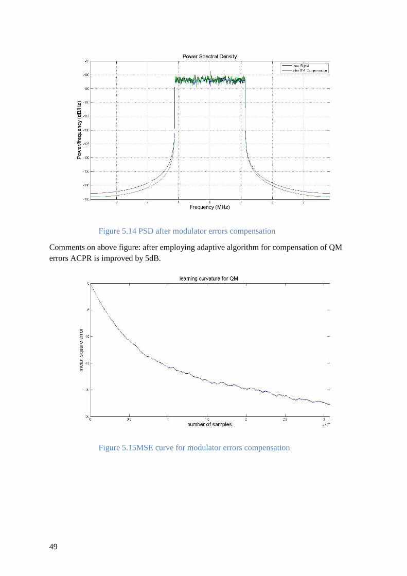
49
Figure 5.14 PSD after modulator errors compensation
Comments on above figure: after employing adaptive algorithm for compensation of QM
errors ACPR is improved by 5dB.
Figure 5.15MSE curve for modulator errors compensation

50
5.4 Adaptive QM and QDM impairments compensation Now demodulator errors are introduced in the circuit. In this case we consider modulator (red
box) and demodulator errors (red box).
The block diagram of the adaptive QM and QDM error compensation is shown in Figure
5.16.
Figure 5.16 Adaptive QMC for compensation of modulator and demodulator errors
Working Procedure: The working procedure is same as 5.2, i.e. demodulator errors are
compensated by using a Hilbert filter.
We now test the above scheme using a complex signal as input and later we use LTE signal
as input.
Operation 1:
Input signal: complex input with fundamental tone of 100 kHz, gain error = 0.3, phase error =
10° and dc offset = 0.05+ 0.05j.
The modulator errors are compensated using the simulation chain developed at 4.4.2 model 2
and demodulator errors are compensated by using the Hilbert filter.
The response for after modulator and demodulator errors is shown in Figure 5.17 in dB.
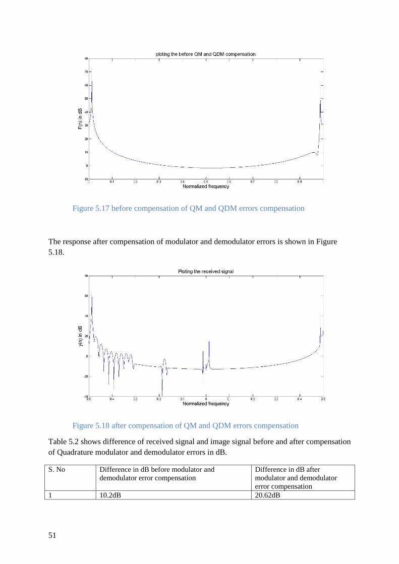
51
Figure 5.17 before compensation of QM and QDM errors compensation
The response after compensation of modulator and demodulator errors is shown in Figure
5.18.
Figure 5.18 after compensation of QM and QDM errors compensation
Table 5.2 shows difference of received signal and image signal before and after compensation
of Quadrature modulator and demodulator errors in dB.
S. No Difference in dB before modulator and
demodulator error compensation
Difference in dB after
modulator and demodulator
error compensation
1 10.2dB 20.62dB
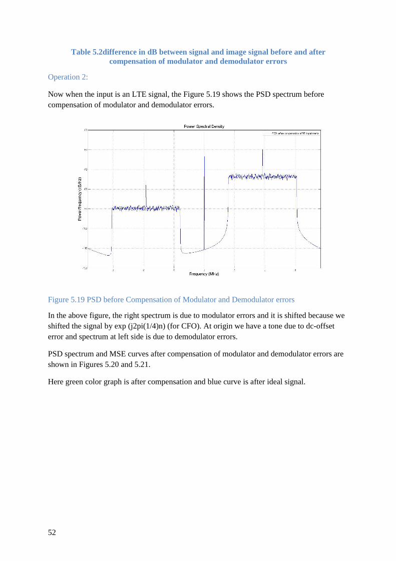
52
Table 5.2difference in dB between signal and image signal before and after
compensation of modulator and demodulator errors
Operation 2:
Now when the input is an LTE signal, the Figure 5.19 shows the PSD spectrum before
compensation of modulator and demodulator errors.
Figure 5.19 PSD before Compensation of Modulator and Demodulator errors
In the above figure, the right spectrum is due to modulator errors and it is shifted because we
shifted the signal by exp (j2pi(1/4)n) (for CFO). At origin we have a tone due to dc-offset
error and spectrum at left side is due to demodulator errors.
PSD spectrum and MSE curves after compensation of modulator and demodulator errors are
shown in Figures 5.20 and 5.21.
Here green color graph is after compensation and blue curve is after ideal signal.
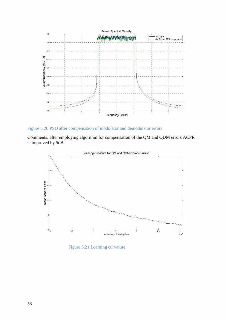
53
Figure 5.20 PSD after compensation of modulator and demodulator errors
Comments: after employing algorithm for compensation of the QM and QDM errors ACPR
is improved by 5dB.
Figure 5.21 Learning curvature
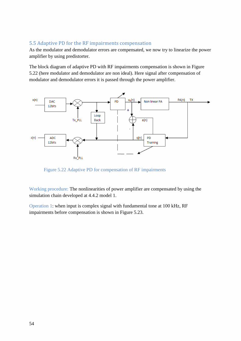
54
5.5 Adaptive PD for the RF impairments compensation As the modulator and demodulator errors are compensated, we now try to linearize the power
amplifier by using predistorter.
The block diagram of adaptive PD with RF impairments compensation is shown in Figure
5.22 (here modulator and demodulator are non ideal). Here signal after compensation of
modulator and demodulator errors it is passed through the power amplifier.
Figure 5.22 Adaptive PD for compensation of RF impairments
Working procedure: The nonlinearities of power amplifier are compensated by using the
simulation chain developed at 4.4.2 model 1.
Operation 1: when input is complex signal with fundamental tone at 100 kHz, RF
impairments before compensation is shown in Figure 5.23.

55
Figure 5.23 before compensation of RF impairments
The Figure 5.24 shows the adaptive PD for RF impairments after compensation.
Figure 5.24 after compensation of RF impairments
Table 5.3 shows difference of received signal and image signal before and after adaptive PD
for RF impairments compensation in dB.
S. No Difference in dB before RF impairments
compensation
Difference in dB adaptive PD
with RF impairments
compensation
1 3dB 17.5dB
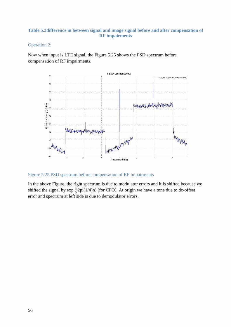
56
Table 5.3difference in between signal and image signal before and after compensation of
RF impairments
Operation 2:
Now when input is LTE signal, the Figure 5.25 shows the PSD spectrum before
compensation of RF impairments.
Figure 5.25 PSD spectrum before compensation of RF impairments
In the above Figure, the right spectrum is due to modulator errors and it is shifted because we
shifted the signal by exp (j2pi(1/4)n) (for CFO). At origin we have a tone due to dc-offset
error and spectrum at left side is due to demodulator errors.
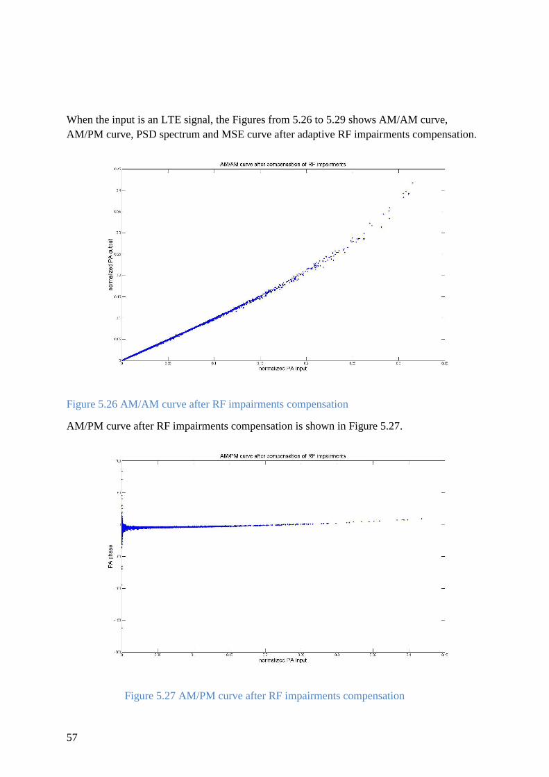
57
When the input is an LTE signal, the Figures from 5.26 to 5.29 shows AM/AM curve,
AM/PM curve, PSD spectrum and MSE curve after adaptive RF impairments compensation.
Figure 5.26 AM/AM curve after RF impairments compensation
AM/PM curve after RF impairments compensation is shown in Figure 5.27.
Figure 5.27 AM/PM curve after RF impairments compensation
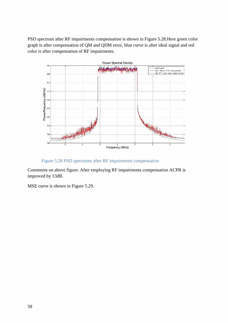
58
PSD spectrum after RF impairments compensation is shown in Figure 5.28.Here green color
graph is after compensation of QM and QDM error, blue curve is after ideal signal and red
color is after compensation of RF impairments.
Figure 5.28 PSD spectrums after RF impairments compensation
Comments on above figure: After employing RF impairments compensation ACPR is
improved by 13dB.
MSE curve is shown in Figure 5.29.
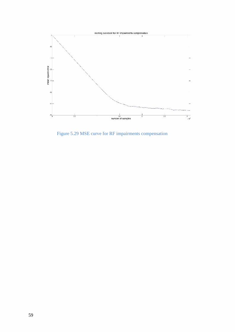
59
Figure 5.29 MSE curve for RF impairments compensation
60
Chapter 6: Conclusion and Future Work
In the transmitters, the power amplifier are the main source for introducing nonlinearities in
the system, further to this, analog implementation of the Quadrature modulator suffers from
many distortions, at the same time receiver also suffers from Quadrature demodulator
impairments, which all together degrades the performance of mobile communication systems.
Nonlinearities not only introduce errors in the data but also lead to spreading of signal
spectrum which in turn leads to the adjacent channel interference.
The thesis work was organized in two phases: in the first phase a bibliography on available
literature is documented and later a simulation chain for an adaptive algorithm for
compensation of the Radio Frequency impairments is developed using MATLAB software.
Chapter 3 discusses about the various linearization techniques availability for the
compensation of the power amplifier nonlinearity. Out of all the available techniques it can
be concluded that the digital predistortion is the suitable method for linearization of power
amplifier as they are flexible, less cost of production and their correction capability. The main
idea of digital predistortion is to produce a nonlinear device whose transfer function is
inverse to the power amplifier, so that when the predistorter and power amplifier are
cascaded together we get a linear output. The predistorter can be realized in two ways, either
by using direct learning architecture or by indirect learning architecture. However in this
thesis we have adopted indirect learning architecture as it is advantageous when compared to
direct learning architecture and predistorter parameters are found through NLMS algorithm.
Finally at the end of chapter a bibliography on available references is documented.
In chapter 4 a simulation chain for compensation of the RF impairments compensation is
developed. Simulation chain is done in 3 states: in the first state only the power amplifier
nonlinearities are considered and a suitable adaptive algorithm is developed for its
compensation, in this procedure we have achieved an improvement of 8dB in ACPR, in the
second state, algorithm for adaptive RF impairments compensation is developed (assuming
ideal demodulator), using this procedure we have achieved an improvement of 10dB in
ACPR, in the third state, algorithm for adaptive RF impairments compensation is developed
(assuming ideal modulator), using this procedure we have achieved an improvement of 10dB
in ACPR.
It was observed that a only a few references have been found that have developed an adaptive
algorithm for compensating the RF impairments in transceivers either by assuming modulator
or demodulator to be ideal. But none have developed an algorithm by considering modulator
and demodulator errors together.
61
So, in this thesis we have tried to develop an algorithm for compensation of the RF
impairments by considering impairments produced by analog modulator and demodulator and
power amplifier nonlinearities.
By using the loop back features of Lime LMS 6002D architecture, it is possible to separate
the problems of the Quadrature modulator (QM) and Quadrature demodulator (QDM) errors
from the rest of the RF impairments. However in the Thesis work Lime LMS 6002D chip
wasn‟t used, as the work was optional. So, in the Thesis work, algorithm is developed in
Matlab software by assuming the LMS 6002D architecture.
It is performed by sequential compensation of all the RF impairments.
1. Compensating the QM and QDM
2. Compensating the PA amplifier nonlinearity.
This idea is documented in chapter 5, using this procedure we have achieved an improvement
in ACPR by 13dB after compensation of the RF impairments.
It can be stated that through the experimental results digital predistorter is the suitable method
for compensation of the RF impairments in transceivers.
In future work, it will be interesting to include quantization errors and further improvement in
adaptation algorithm for faster convergence.
62
REFERENCES
[1] E. Armstrong, “A method of reducing disturbances in radio signaling by a system of
frequency modulation,” Proceedings of the IRE, vol.24, 1936, pp.689-740.
[2] P. Kenington, “Introduction,” in High linearity RF amplifier design, Northwood, Artech
House, 2000, pp. 8-9.
[3] S. Cripps, “Introduction”, in RF power amplifiers for wireless communications,
Northwood, Artech House, 1999, pp. 10-12
[4] M. Albulet, “classs AB amplifier”, in RF power systems, Atlanta, Noble Publishing,
2001, pp. 4-5.
[5] S. Cripps, “Introduction”, in RF power amplifiers for wireless communications,
Northwood, Artech House, 1999, pp. 10-12.
[6] S. Stapleton and J. Cavers, “A new technique for adaptation of linearizing Predistorters,”
IEEE 41nd Vehicular technology Conference, pp. 753-758, May 1991.
[7] A. Saleh, “Frequency- independent and frequency-dependent non linear models of TWT
amplifiers,” IEEE Transactions on Communications, Vol. 29, pp. 1715-1720, 1981.
[8] C. Raap “Effects of HPA-nonlinearity on a 4-DPSK/OFDM-signal for digital sound
broad-casting system,” In ESA, Second European Conference on Satellite Communications
(ECSC-2) pp. 179-184.
[9] D.Falconer, T. Kolze, Y. Leiba, and J. Liebetreu, “IEEE 802.16.1 proposed system
impairment models, slide supplement,” IEEE, Tech., 2000.
[11] H. Black, “Translating system”, U.S Patent 1,686,792, October 1928.
[12] L. Kahn, “Single-sideband transmission by envelope elimination and restoration,”
proceedings of the IRE, Vol.40, pp. 803-806, 1952.
[13] F.H. Raab, P. Asbeck, S. Cripps, P.B. Kenington, Z.B. Popovic, N. Pothecary, J.F.
Service, N. O. Sokal, “Power amplifier and transmitter for RF abd microwave,” IEEE
transaction on Microwave Theory and Techniques, Vol. 50, pp.814-826, Mar. 2002.
63
[14] Y. Nagata, “Linear amplification technique for digital mobile communications,” in
proceedings of IEEE Vehicular Technology Conference, San Francisco, USA, May 1989,
Vol.1, pp. 159-164.
[15] J. Cavers, “Amplifier linearization using a digital predistorter with fast adaptation and
low memory requirements,” IEEE Transactions on Vehicular Technology, Vol. 39, pp.374-
382, November 1990.
[16] “ESTI Digital Video Broadcasting; Framing Structure, Channel Coding and Modulation
for Digital TV,” 2004.
[17] M. Faulkner, M. Johansson, “Adaptive linearization using predistortion experiment
results,” IEEE Transactions Vehicular Technology, Vol. 43, No. 2, pp. 447-450, May 1994.
[18] J. K Cavers, M. W. Liao, “Adaptive compensation for imbalance and offset losses in
direct conversion transceivers,” IEEE Trans. Veh. Technology, Vol. 42, No. 4, pp. 581-588,
Nov 1993.
[19] D. Giesbers, S. Mann, K. Eccleston, “Adaptive digital predistortion linearization for RF
power amplifiers,” Electronics New Zealand Conference 2006.
[20] G. Rahul gupta, S. Ahmad, R. Ludwig, J. McNeil, “Adaptive DPD for PA
nonlinearities,”High Frequency Electronics Summit Technical Media, LLC, 2006.
[21] S. Amandeep Singh, S. Manjit Singh and S. Sanjay , “Digital predistortion for power
amplifier with memory effects,” ICGST-PDCS, Volume 8, Issue 1, Dec 2008.
[22] E. EmadAbd, “Adaptive Predistortion of Wiener and Hammerstein systems using
spectral magnitude matching,” Christian Doppler Laboratory for Nonlinear Signal Processing
Institute of Signal Processing and Speech Communication.
[23] D. Yuanming , S. Akira , “Time domain predistortion for nonlinear amplifiers.”
[24] C. Ammar, A. Myriam, T. Sylvain , G. Jean-Luc , “ adaptive compensation of high
frequency memory effects of a realistic amplifier in an OFDM system,” in proceedings of
IEEE, Vol.2, pp 2629-2633, 2006.
[25] Z. Jing , H. Songbai Y. Shirong , “A memory polynomial predistorter for compensation
of nonlinearities with memory effects in WCDMA transmitters,” IEEE, pp 913-916, 2009.
[26] W. Marcus , F. Gerhard, “Adaptive I/Q imbalance compensation in Low-IF transmitter
architectures,”Dresden University of Technology Vodafone Chair Mobile Communications
Systems.
[27] T. Jan C. Boris, V. Liesbet , D. Luc , D. Stephane, E. Marc “Compensation of IQ
imbalance in OFDM systems,” IEEE, Vol. 5, pp. 3304-3307, 2003.
[28] M. Mailand, R. Richter, H.J. Jentschel “IQ-imbalance and its compensation for non-ideal
analog receivers comprising frequency-selective components.”Dresden University of
Technology, Institute of Traffic Information Systems, 2006.
[29] T. Deepaknath, M. Marc , “Efficient compensation of transmitter and receiver IQ
imbalance in OFDM systems,” EURASIP Journal on Advances in Signal Processing,
Belgium, 2010.
64
[30] A. Lauri, H. Peter, V. Mikko “Joint mitigation of power amplifier and I/Q modulator
impairments in broadband direct conversion transmitters,” IEEE transactions on microwave
theory and techniques, Volume 58, No 4, pp. 730-739, April 2010.
[31] W. Marcus, F. Gerhard, “Blind Imbalance parameter estimation and compensation in
Low-IF receivers,” IEEE Control, Communication and Signal Processing, pp.75-78, 2004.
[32] L, Mika, K. Adrian, H. Atso, J. Pertti, M. Aarne, “Adaptive predistortion architecture for
non ideal radio transmitter,” IEEE Transactions Vehicular Technology Conference, pp. 1256-
1260, 2008.
[33] K. -Doo, J. Eui-Rim, N. Taegyun and L. Yong, “Joint adaptive compensation for
amplifier nonlinearity and quadrature modulation errors” IEEE Transactions Vehicular
Technology Conference, Vol. 5, pp. 2290-2293, 2006.
[34] Z. Hassan, V. Vahidtabataba, “New Adaptive method for IQ imbalance compensation
modulators in predistortion systems,” EURASIP Journal, Tehran, 2009.
[35] K. Young-Doo, J. Eui-Rim, L. Yong, “Adaptive compensation for power amplifier
nonlinearity in presence of Quadrature Modulation/Demodulation Errors,” IEEE Transactions
on signal processing, Vol. 55, No. 9, pp. 4717-4721, September 2007.
[36] B. Sascha, P. Michael, S. Andreas, H. Gernot, “Joint distortion compensation for direct
up conversion transmitter with impairments,” IEEE wireless information Technology, pp. 1-
4, 2010.
[37] H. Peter, Z. Per, “Receiver I/Q Imbalance: tone test, sensitivity analysis and the
universal software radio peripheral,” IEEE Transactions on Instrumentation and
measurement, Vol. 59, No. 3, pp. 704-714, March 2010.
[38] P. Henna, M. Aame, “Comparison of direct learning and indirect learning predistortion
architectures,” in the proceedings of IEEE, pp. 309-313, 2008.
65
LIST OF SYMBOLS & ABBREVIATIONS
()*: Complex conjugate
GPA = Gain of power amplifier
() H
: Hermitian matrix
Mu: Adaptive Filter convergence coefficient
ΦPA = Phase of power amplifier
ACPR: Adjacent channel power ratio
AM/AM: Amplitude to amplitude
A/D: Analog to digital
DPD: Digital Predistortion
D/A: Digital to analog
EER: Envelop elimination and restoration
EVM: Error vector magnitude
EDGE: Enhanced data rates for GSM system
GSM: Global system for communications
I/Q: Inphase / Quadrature phase
IMD: Inter-modulation distortion
LINC: Linear Amplification using Nonlinear Components
LMS: Least mean square
LTE: Long term evolution
NL: Nonlinearity
NLMS: Normalized least mean square
OFDM: Orthogonal frequency division multiplexing

66
PA: Power Amplifier
PD: Predistortion
QAM: Quadrature amplitude modulation
QDM: Quadrature Demodulator
QM: Quadrature Modulator
RF: Radio frequency
RLS: Recursive least mean square
THD: Total harmonic distortion
CFO: Carrier frequency offset
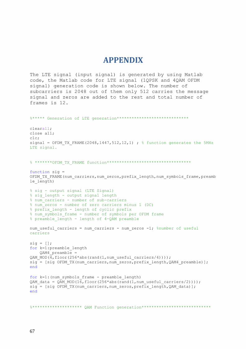
67
APPENDIX
The LTE signal (input signal) is generated by using Matlab
code, the Matlab code for LTE signal (1QPSK and 4QAM OFDM
signal) generation code is shown below. The number of
subcarriers is 2048 out of them only 512 carries the message
signal and zeros are added to the rest and total number of
frames is 12.
%***** Generation of LTE generation*****************************
clearall;
close all; clc; signal = OFDM_TX_FRAME(2048,1447,512,12,1) ; % function generates the 5MHz
LTE signal.
% *******OFDM_TX_FRAME function**********************************
function sig =
OFDM_TX_FRAME(num_carriers,num_zeros,prefix_length,num_symbols_frame,preamb
le_length)
% sig - output signal (LTE Signal) % sig_length - output signal length % num_carriers - number of sub-carriers % num_zeros - number of zero carriers minus 1 (DC) % prefix_length - length of cyclic prefix % num_symbols_frame - number of symbols per OFDM frame % preamble_length - length of 4-QAM preamble
num_useful_carriers = num_carriers - num_zeros -1; %number of useful
carriers
sig = []; for k=1:preamble_length QAM4_preamble =
QAM_MOD(4,floor(256*abs(rand(1,num_useful_carriers/4)))); sig = [sig OFDM_TX(num_carriers,num_zeros,prefix_length,QAM4_preamble)]; end
for k=1:(num_symbols_frame - preamble_length) QAM_data = QAM_MOD(16,floor(256*abs(rand(1,num_useful_carriers/2)))); sig = [sig OFDM_TX(num_carriers,num_zeros,prefix_length,QAM_data)]; end
%******************** QAM Function generation****************************

68
function [sig,sig_length] = QAM_MOD(size,input)
% sig - output symbols % size - modulation size (4,16,256) % input - vector of bytes to be modulated
AM2 = [-1 1]; AM4 = [-3 -1 1 3]; AM4 = 2*AM4/sqrt(AM4*AM4'); AM16 = [-15 -13 -11 -9 -7 -5 -3 -1 1 3 5 7 9 11 13 15];
AM16 = 4*AM16/sqrt(AM16*AM16');
sig = zeros(1,length(input)*8/log2(size)); sig_length = length(input)*8/log2(size);
for l=1:length(input) if (size == 256) % for modulation size of 256 sig(l) = (AM16(1+ floor((input(l)/16))) +sqrt(-
1)*AM16(1+rem(input(l),16)))/sqrt(2);
elseif (size == 16) % for modulation size of 16 sig(1 + 2*(l-1)) = (AM4(1+floor((input(l)/64))) + sqrt(-
1)*AM4(1+rem(floor(input(l)/16) , 4)))/sqrt(2); sig(2 + 2*(l-1)) = (AM4(1+rem(floor(input(l)/4) , 4)) + sqrt(-
1)*AM4(1+rem(input(l) , 4)))/sqrt(2);
elseif (size == 4) % for modulation size of 4 sig(1+ 4*(l-1)) = (AM2(1+(floor(input(l)/128))) + sqrt(-
1)*AM2(1+rem(floor(input(l)/64) , 2)))/sqrt(2); sig(2+ 4*(l-1)) = (AM2(1+rem(floor(input(l)/32) ,2)) + sqrt(-
1)*AM2(1+rem(floor(input(l)/16) , 2)))/sqrt(2); sig(3+ 4*(l-1)) = (AM2(1+rem(floor(input(l)/8) , 2)) + sqrt(-
1)*AM2(1+rem(floor(input(l)/4) , 2)))/sqrt(2); sig(4+ 4*(l-1)) = (AM2(1+rem(floor(input(l)/2) , 2)) + sqrt(-
1)*AM2(1+rem(input(l) , 2)))/sqrt(2);
end end
%************** OFDM_TX function**************
function [sig,sig_length] =
OFDM_TX(num_carriers,num_zeros,prefix_length,input)
% OFDM Transmitter - DC removed % sig is the output signal % length is the length of the output signal % num_carriers - number of sub-carriers (power of 2) % num_zeros - number of zeros minus 1 (DC) in output spectrum (odd) % prefix_length - length of cyclic prefix % input - input dimensions (length = number_carriers - num_zeros - 1)
if (length(input) + num_zeros + 1 ~= num_carriers) fprintf('error in lengths\n'); return; end
ext_input = [0 input(1:length(input)/2) zeros(1,num_zeros)
input((1+length(input)/2) : length(input))];
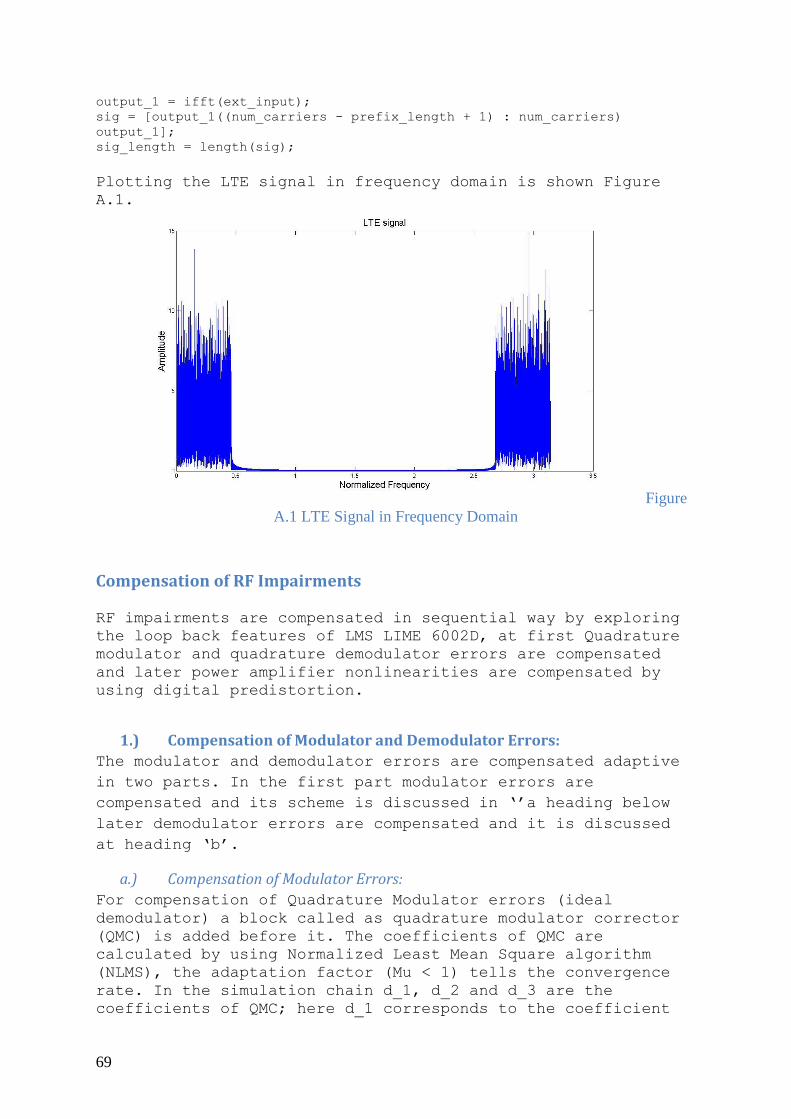
69
output_1 = ifft(ext_input); sig = [output_1((num_carriers - prefix_length + 1) : num_carriers)
output_1]; sig_length = length(sig);
Plotting the LTE signal in frequency domain is shown Figure
A.1.
Figure
A.1 LTE Signal in Frequency Domain
Compensation of RF Impairments
RF impairments are compensated in sequential way by exploring
the loop back features of LMS LIME 6002D, at first Quadrature
modulator and quadrature demodulator errors are compensated
and later power amplifier nonlinearities are compensated by
using digital predistortion.
1.) Compensation of Modulator and Demodulator Errors:
The modulator and demodulator errors are compensated adaptive
in two parts. In the first part modulator errors are
compensated and its scheme is discussed in ‘’a heading below
later demodulator errors are compensated and it is discussed
at heading ‘b’.
a.) Compensation of Modulator Errors:
For compensation of Quadrature Modulator errors (ideal
demodulator) a block called as quadrature modulator corrector
(QMC) is added before it. The coefficients of QMC are
calculated by using Normalized Least Mean Square algorithm
(NLMS), the adaptation factor (Mu < 1) tells the convergence
rate. In the simulation chain d_1, d_2 and d_3 are the
coefficients of QMC; here d_1 corresponds to the coefficient
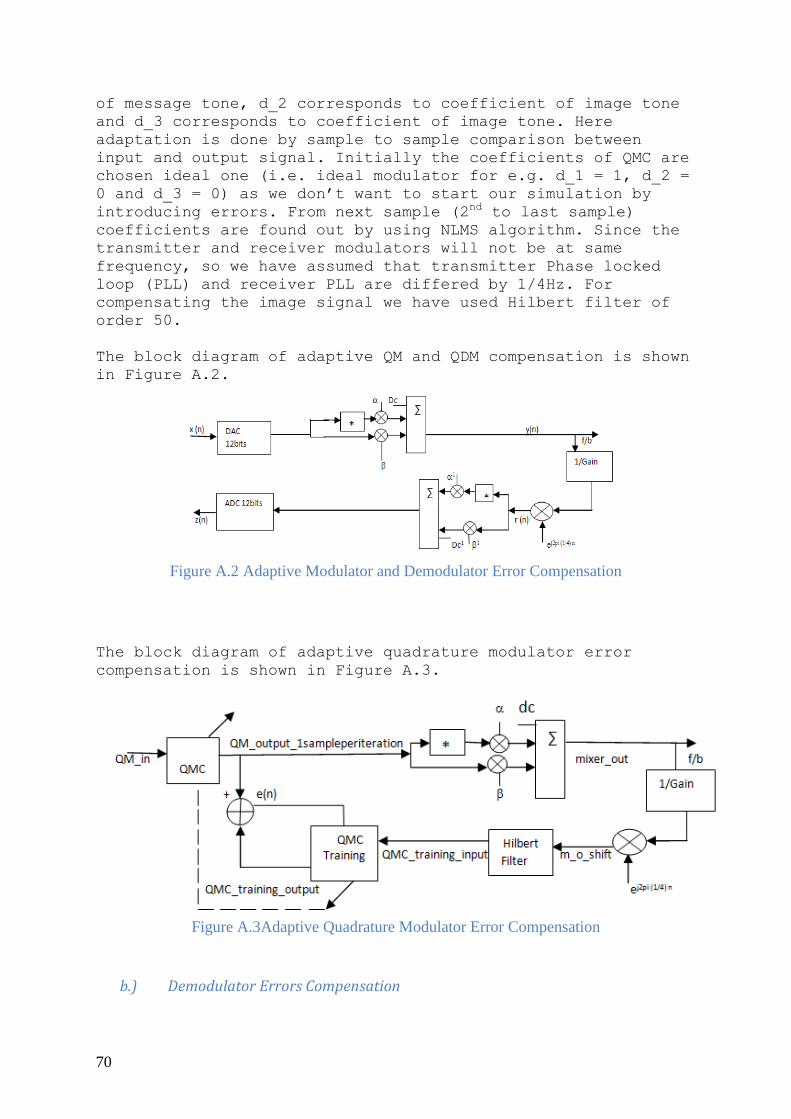
70
of message tone, d_2 corresponds to coefficient of image tone
and d_3 corresponds to coefficient of image tone. Here
adaptation is done by sample to sample comparison between
input and output signal. Initially the coefficients of QMC are
chosen ideal one (i.e. ideal modulator for e.g. d_1 = 1, d_2 =
0 and d_3 = 0) as we don’t want to start our simulation by
introducing errors. From next sample (2nd to last sample)
coefficients are found out by using NLMS algorithm. Since the
transmitter and receiver modulators will not be at same
frequency, so we have assumed that transmitter Phase locked
loop (PLL) and receiver PLL are differed by 1/4Hz. For
compensating the image signal we have used Hilbert filter of
order 50.
The block diagram of adaptive QM and QDM compensation is shown
in Figure A.2.
Figure A.2 Adaptive Modulator and Demodulator Error Compensation
The block diagram of adaptive quadrature modulator error
compensation is shown in Figure A.3.
Figure A.3Adaptive Quadrature Modulator Error Compensation
b.) Demodulator Errors Compensation
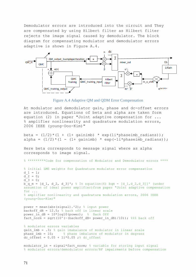
71
Demodulator errors are introduced into the circuit and They
are compensated by using Hilbert filter as Hilbert filter
rejects the image signal caused by demodulator. The block
diagram for compensating modulator and demodulator errors
adaptive is shown in Figure A.4.
Figure A.4 Adaptive QM and QDM Error Compensation
At modulator and demodulator gain, phase and dc-offset errors
are introduced. Equations of beta and alpha are taken form
equation (2) in paper "Joint adaptive compensation for ...
% amplifier nonlinearity and quadrature modulation errors,
2006 IEEE (young-Doo-Kim)"
beta = (1/2)*(1 + (1+ gainimb) * exp(1i*phaseimb_radians));
alpha = (1/2)*(1 - (1+ gainimb) * exp(-1i*phaseimb_radians));
Here beta corresponds to message signal where as alpha
corresponds to image signal.
% *********Code for compensation of Modulator and Demodulator errors ****
% initial LMS weights for Quadrature modulator error compensation d_1 = 1; d_2 = 0; d_3 = 0; b_q_m = [d_1, d_2, d_3]'; % In equation(6) bqm = [d_1,d_2,d_3]]' (under
assumtion of ideal power amplifier)from paper "Joint adaptive compensation
for ... % amplifier nonlinearity and quadrature modulation errors, 2006 IEEE
(young-Doo-Kim)"
power = mean(abs(signal).^2); % input power backoff_dB = 12.5; % back off in linear scale power_in_dB = 10*log10(power); % Back Off fact_norm = sqrt(10^(-(backoff_dB+ power_in_dB)/10)); %%% back off
% modulator errors variables gain_imb = .3; % gain imabalance of modulator in linear scale phase_imb = 10; % phase imbalance of modulator in degrees dc_offset = 0.05 + 1i*0.05 ;% dc_offset
modulator_in = signal*fact_norm; % variable for storing input signal % modulator errors/demodulator errors/RF impairments before compensation

72
PA_input_before_compensation =
modulator(modulator_in,gain_imb,phase_imb,dc_offset); % modulator function
for introducing modulator errors
demod_output =
demodulator(PA_input_before_compensation,gain_imb,phase_imb,dc_offset); %
demodulator function for introducing demodulator errors
% plotting of figures % plotting of spectrum before compensation Fs= 7.68e6; hPsd2 = spectrum.welch('Blackman',2048); hopts2 = psdopts(hPsd2); set(hopts2,'SpectrumType','twosided','NFFT',2048,'Fs',Fs,..., 'CenterDC',true); PSD3 = psd(hPsd2,demod_output,hopts2); data = dspdata.psd([PSD3.Data],PSD3.Frequencies,'Fs',Fs); figure(12); plot(data); legend('PSD of QM and QDM before compensation');
% Error Vector magnitude (EVM) before compensation
Vmax = max(abs(modulator_in)); EVM_before_compensation_RF_impairments = 0; EVM_before_compensation_RF_impairments =
EVM_before_compensation_RF_impairments + mean(abs(demod_output -
modulator_in).^2); EVM_before_compensation_RF_impairments =
sqrt(EVM_before_compensation_RF_impairments)/ Vmax
figure(1); plot((((abs(demod_output).^2))),(((abs(modulator_in).^2))),'r');
title('AM/AM curve before QM and QDM compensation') xlabel('input'); ylabel('output'); hold on;
figure(2) phasediff3 = 360/(2*pi)*(wrapToPi(angle(demod_output)-
angle(modulator_in))); plot((((abs(modulator_in).^2))),phasediff3,'r');
title('AM/PM curve before QM and QDM compensation') xlabel('input'); ylabel('phase'); hold on;
% initilization of variables before compensation
filter_length =50; % assumtion of Hilbert Filter length modulator_in = [zeros(1,filter_length),modulator_in]; % adding zeros
before input for delayed input signal (this is needed for Hilbert Filter) QM_output_1sample_per_iteration = zeros(1,length(signal)+filter_length+1);
% Quadrature modulator(QM)output % PA_output = zeros(1,length(signal)+filter_length+1); % power
amplifier(PA) function QMC_training_input= zeros(1,length(signal)+filter_length+1); QMC_training_output= zeros(1,length(signal)+filter_length+1); mixer_out = zeros(1,length(signal)+filter_length+1); input = zeros(1,filter_length); % input signal for Hilbert Filter
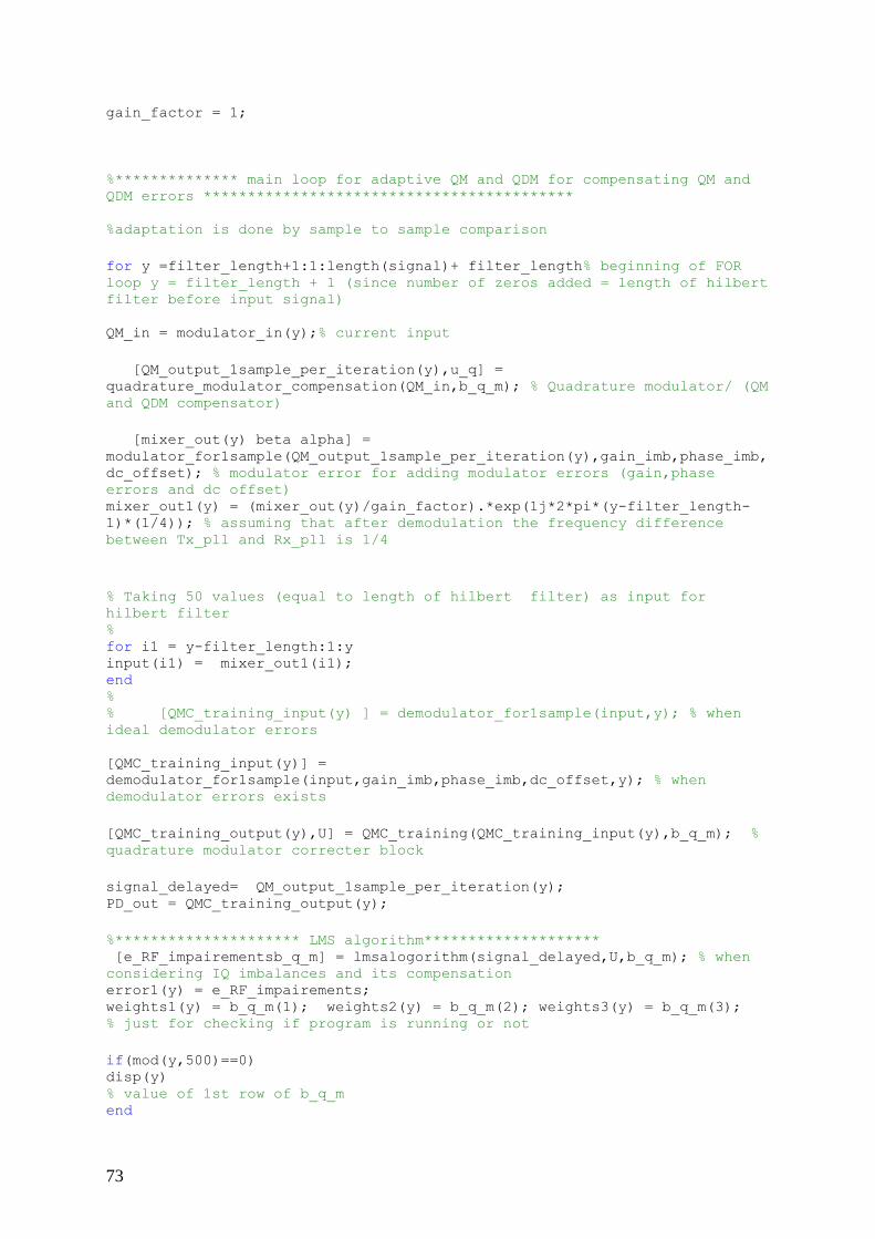
73
gain_factor = 1;
%************** main loop for adaptive QM and QDM for compensating QM and
QDM errors ******************************************
%adaptation is done by sample to sample comparison
for y =filter_length+1:1:length(signal)+ filter_length% beginning of FOR
loop y = filter_length + 1 (since number of zeros added = length of hilbert
filter before input signal)
QM_in = modulator_in(y);% current input
[QM_output_1sample_per_iteration(y),u_q] =
quadrature_modulator_compensation(QM_in,b_q_m); % Quadrature modulator/ (QM
and QDM compensator)
[mixer_out(y) beta alpha] =
modulator_for1sample(QM_output_1sample_per_iteration(y),gain_imb,phase_imb,
dc_offset); % modulator error for adding modulator errors (gain,phase
errors and dc offset) mixer_out1(y) = (mixer_out(y)/gain_factor).*exp(1j*2*pi*(y-filter_length-
1)*(1/4)); % assuming that after demodulation the frequency difference
between Tx_pll and Rx_pll is 1/4
% Taking 50 values (equal to length of hilbert filter) as input for
hilbert filter % for i1 = y-filter_length:1:y input(i1) = mixer_out1(i1); end % % [QMC_training_input(y) ] = demodulator_for1sample(input,y); % when
ideal demodulator errors
[QMC_training_input(y)] =
demodulator_for1sample(input,gain_imb,phase_imb,dc_offset,y); % when
demodulator errors exists
[QMC_training_output(y),U] = QMC_training(QMC_training_input(y),b_q_m); %
quadrature modulator correcter block
signal_delayed= QM_output_1sample_per_iteration(y); PD_out = QMC_training_output(y);
%********************* LMS algorithm******************** [e_RF_impairementsb_q_m] = lmsalogorithm(signal_delayed,U,b_q_m); % when
considering IQ imbalances and its compensation error1(y) = e_RF_impairements; weights1(y) = b_q_m(1); weights2(y) = b_q_m(2); weights3(y) = b_q_m(3); % just for checking if program is running or not
if(mod(y,500)==0) disp(y) % value of 1st row of b_q_m end
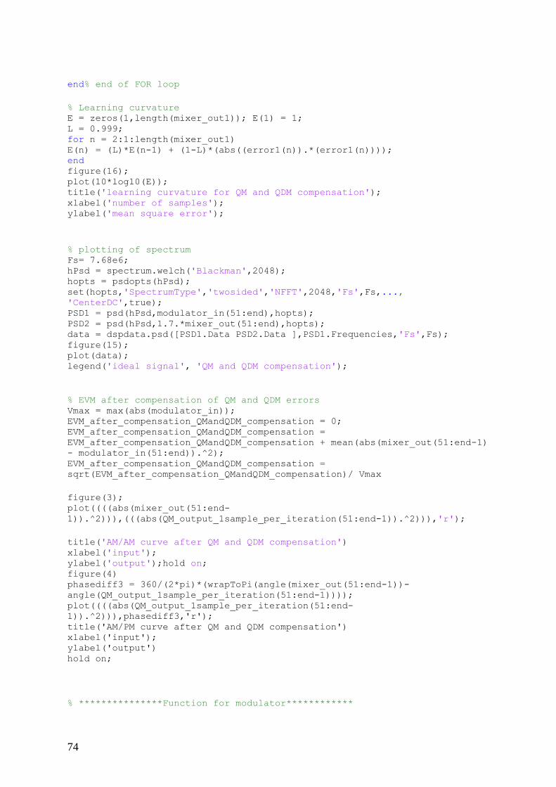
74
end% end of FOR loop
% Learning curvature E = zeros(1,length(mixer_out1)); E(1) = 1; L = 0.999; for n = 2:1:length(mixer_out1) E(n) = (L)*E(n-1) + (1-L)*(abs((error1(n)).*(error1(n)))); end figure(16); plot(10*log10(E)); title('learning curvature for QM and QDM compensation'); xlabel('number of samples'); ylabel('mean square error');
% plotting of spectrum Fs= 7.68e6; hPsd = spectrum.welch('Blackman',2048); hopts = psdopts(hPsd); set(hopts,'SpectrumType','twosided','NFFT',2048,'Fs',Fs,..., 'CenterDC',true); PSD1 = psd(hPsd,modulator_in(51:end),hopts); PSD2 = psd(hPsd,1.7.*mixer_out(51:end),hopts); data = dspdata.psd([PSD1.Data PSD2.Data ],PSD1.Frequencies,'Fs',Fs);
figure(15); plot(data); legend('ideal signal', 'QM and QDM compensation');
% EVM after compensation of QM and QDM errors
Vmax = max(abs(modulator_in)); EVM_after_compensation_QMandQDM_compensation = 0; EVM_after_compensation_QMandQDM_compensation =
EVM_after_compensation_QMandQDM_compensation + mean(abs(mixer_out(51:end-1)
- modulator_in(51:end)).^2); EVM_after_compensation_QMandQDM_compensation =
sqrt(EVM_after_compensation_QMandQDM_compensation)/ Vmax
figure(3); plot((((abs(mixer_out(51:end-
1)).^2))),(((abs(QM_output_1sample_per_iteration(51:end-1)).^2))),'r');
title('AM/AM curve after QM and QDM compensation') xlabel('input'); ylabel('output');hold on; figure(4) phasediff3 = 360/(2*pi)*(wrapToPi(angle(mixer_out(51:end-1))-
angle(QM_output_1sample_per_iteration(51:end-1)))); plot((((abs(QM_output_1sample_per_iteration(51:end-
1)).^2))),phasediff3,'r'); title('AM/PM curve after QM and QDM compensation') xlabel('input'); ylabel('output') hold on;
% ***************Function for modulator************
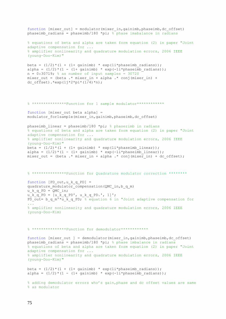
75
function [mixer_out] = modulator(mixer_in,gainimb,phaseimb,dc_offset) phaseimb_radians = phaseimb/180 *pi; % phase imabalance in radians
% equations of beta and alpha are taken form equation (2) in paper "Joint
adaptive compensation for ... % amplifier nonlinearity and quadrature modulation errors, 2006 IEEE
(young-Doo-Kim)"
beta = (1/2)*(1 + (1+ gainimb) * exp(1i*phaseimb_radians)); alpha = (1/2)*(1 - (1+ gainimb) * exp(-1i*phaseimb_radians)); n = 0:30719; % as number of input samples = 30720 mixer_out = (beta .* mixer_in + alpha .* conj(mixer_in) +
dc_offset).*exp(1j*2*pi*(1/4)*n);
% ***************Function for 1 sample modulator************
function [mixer_out beta alpha] =
modulator_for1sample(mixer_in,gainimb,phaseimb,dc_offset)
phaseimb_linear = phaseimb/180 *pi; % phaserimb in radians % equations of beta and alpha are taken form equation (2) in paper "Joint
adaptive compensation for ... % amplifier nonlinearity and quadrature modulation errors, 2006 IEEE
(young-Doo-Kim)" beta = (1/2)*(1 + (1+ gainimb) * exp(1i*phaseimb_linear)); alpha = (1/2)*(1 - (1+ gainimb) * exp(-1i*phaseimb_linear)); mixer_out = (beta .* mixer_in + alpha .* conj(mixer_in) + dc_offset);
% ***************Function for Quadrature modulator correction ********
function [PD_out,u_k_q_PD] =
quadrature_modulator_compensation(QMC_in,b_q_m) u_k_q_PD = QMC_in; u_k_q_PD = [u_k_q_PD', u_k_q_PD.', 1]'; PD_out= b_q_m'*u_k_q_PD; % equation 6 in "Joint adaptive compensation for
... % amplifier nonlinearity and quadrature modulation errors, 2006 IEEE
(young-Doo-Kim)
% ***************Function for demodulator************
function [mixer_out ] = demodulator(mixer_in,gainimb,phaseimb,dc_offset) phaseimb_radians = phaseimb/180 *pi; % phase imbalance in radians % equations of beta and alpha are taken form equation (2) in paper "Joint
adaptive compensation for ... % amplifier nonlinearity and quadrature modulation errors, 2006 IEEE
(young-Doo-Kim)"
beta = (1/2)*(1 + (1+ gainimb) * exp(1i*phaseimb_radians)); alpha = (1/2)*(1 - (1+ gainimb) * exp(-1i*phaseimb_radians));
% adding demodulator errors who’s gain,phase and dc offset values are same % as modulator
76
mixer_out = beta .* mixer_in + alpha .* conj(mixer_in) + dc_offset;
% function of demodulator_for1sample
function [output ] =
demodulator_for1sample(input,gainimb,phaseimb,dc_offset,y) filter_length = 50; x = fliplr(input); % fliping since the present signal starts from 101rd
column input_filter = x(1:end-1); % present input phaseimb_radians = phaseimb/180 *pi; % equations of beta and alpha are taken form equation (2) in paper "Joint
adaptive compensation for ... % amplifier nonlinearity and quadrature modulation errors, 2006 IEEE
(young-Doo-Kim)" beta = (1/2)*(1 + ( (1+gainimb) * exp(1i*phaseimb_radians))); alpha = (1/2)*(1 - ( (1 + gainimb) * exp(-1i*phaseimb_radians))); z_n_1 = (beta*input_filter +alpha*conj(input_filter)+dc_offset); %
demodulator errors
% hilbert filter is used for removing errors caused by demodulator and % selecting the required tones A=firls(49,[0 0.45 0.5 0.8 0.9 1 ],[0 0 1 1 0 0 ]); B=firls(49,[0 0.45 0.5 0.8 0.9 1 ],[0 0 1 1 0 0 ],'hilbert'); C= A+1i*B;
for i1 = 1:1:50
y1(i1) = C(i1)*z_n_1(i1);
end
y2 = sum(y1); %y(n) = c_0*input_filter(n) + c_1 *input_filter(n-1) + c_2
*input_filter(n-2) +......
shifting_tone = exp(1i*2*pi*(-1/4)*(y-filter_length-1)); % for shifting the
tones to origin output = y2*shifting_tone; % since, after loop back the input signal is shifted by 1/4 as difference % betweenTxpllabd Rx pll. so for shifting the tone back to original
position it % should be multiplied with (-1/4)
% *************** function of lms algorithm*******************
function[ error w] = lmsalogorithm(signal_delayed,u_k_q_post_D,w)
mu = 0.001; % adaptation factor hat_y = w'* u_k_q_post_D; % signal after the post distorter/ Qmc training
block error = signal_delayed - hat_y; % normalized LMS method N=sum(abs(u_k_q_post_D).^2)+10^-3;
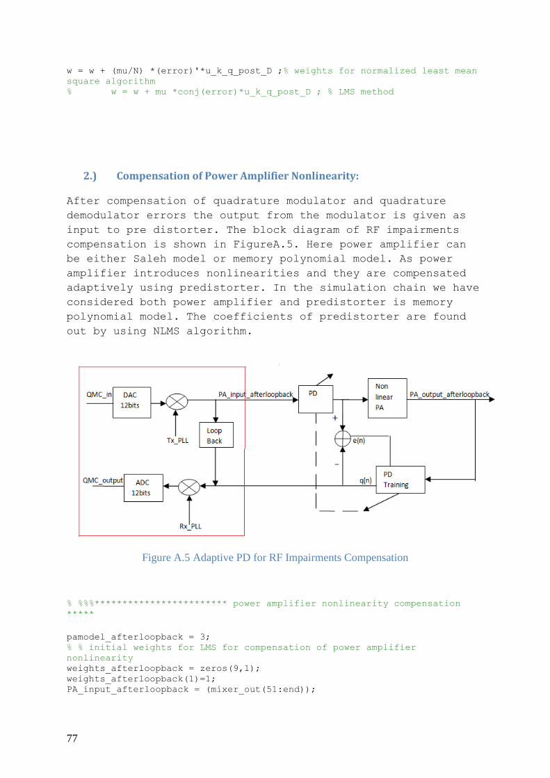
77
w = w + (mu/N) *(error)'*u_k_q_post_D ;% weights for normalized least mean
square algorithm % w = w + mu *conj(error)*u_k_q_post_D ; % LMS method
2.) Compensation of Power Amplifier Nonlinearity:
After compensation of quadrature modulator and quadrature
demodulator errors the output from the modulator is given as
input to pre distorter. The block diagram of RF impairments
compensation is shown in FigureA.5. Here power amplifier can
be either Saleh model or memory polynomial model. As power
amplifier introduces nonlinearities and they are compensated
adaptively using predistorter. In the simulation chain we have
considered both power amplifier and predistorter is memory
polynomial model. The coefficients of predistorter are found
out by using NLMS algorithm.
Figure A.5 Adaptive PD for RF Impairments Compensation
% %%%************************ power amplifier nonlinearity compensation
*****
pamodel_afterloopback = 3; % % initial weights for LMS for compensation of power amplifier
nonlinearity weights_afterloopback = zeros(9,1); weights_afterloopback(1)=1; PA_input_afterloopback = (mixer_out(51:end));

78
PA_input_afterloopback = [zeros(1,2), PA_input_afterloopback ]; % adding 2
zeros before assuming that memory polynomial PA of memory depth = 2 PD_output_1_afterloopback = zeros(1,30722) ; postdistorter_out_afterloopback = zeros(1,30722); PA_output_afterloopback = zeros(1,30722); for x = 3:1:30722 % FOR loop
%%% sample to sample adaptation
predistorter_afterloopback = PA_input_afterloopback(x); % current input predistorter_afterloopback_in_2 = PA_input_afterloopback(x-1); % delayed
input initially it is zero for 1st sample predistorter_afterloopback_in_3 = PA_input_afterloopback(x-2); % delayed
input initially it is zero for 2nd sample [PD_output_1_afterloopback(x),u_q] =
predistorter_demod(predistorter_afterloopback,predistorter_afterloopback_in
_2,predistorter_afterloopback_in_3,weights_afterloopback); % predistortion
function PA_in_1_afterloopback = PD_output_1_afterloopback(x); % 1st sample PA_in_2_afterloopback = PD_output_1_afterloopback(x-1); % 2nd sample PA_in_3_afterloopback =PD_output_1_afterloopback(x-2); % 3rd sample [PA_output_afterloopback(x)] =
poweramplifier(PA_in_1_afterloopback,PA_in_2_afterloopback,PA_in_3_afterloo
pback,pamodel_afterloopback ); % power amplifier function postdistorter_in_1_afterloopback = PA_output_afterloopback(x); % input(1st
sample) of post distorter postdistorter_in_2_afterloopback = PA_output_afterloopback(x-1); %
input(2nd sample) of post distorter postdistorter_in_3_afterloopback = PA_output_afterloopback(x-2); %
input(3rd sample) of post distorter
[postdistorter_out_afterloopback(x),u_k_q_post_D] =
postdistorter(postdistorter_in_1_afterloopback,
postdistorter_in_2_afterloopback,
postdistorter_in_3_afterloopback,weights_afterloopback); % postdistorter
% % ******************* LMS algorithm*******************************
signal_delayed_afterloopback = PD_output_1_afterloopback(x); % signal after
predistorter and QMC block
[eweights_afterloopback] =
lmsalogorithm(signal_delayed_afterloopback,u_k_q_post_D,weights_afterloopba
ck); % [error weights] = lmsalgorithm(1st i/p, 2nd i/p, weights)
error_PA_compensation(x) = e;
weights4(x) = weights_afterloopback(1); weights5(x) =
weights_afterloopback(2); weights6(x) = weights_afterloopback(3); weights7(x) = weights_afterloopback(4); weights8(x) =
weights_afterloopback(5); weights9(x) = weights_afterloopback(6); weights10(x) = weights_afterloopback(7); weights11(x) =
weights_afterloopback(8); weights12(x) = weights_afterloopback(9); if(mod(x,500)==0) disp(x) disp(weights_afterloopback(1)) end
end% end of FOR loop
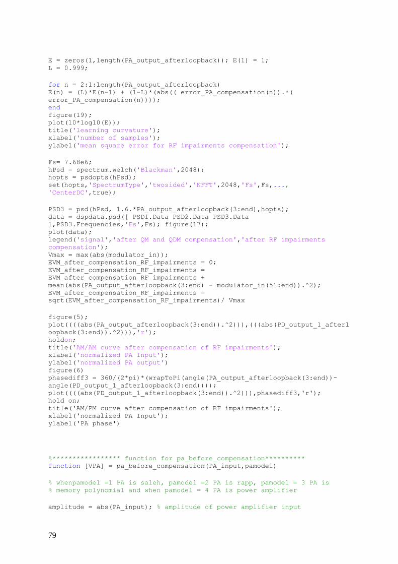
79
E = zeros(1,length(PA_output_afterloopback)); E(1) = 1; L = 0.999;
for n = 2:1:length(PA_output_afterloopback) E(n) = (L)*E(n-1) + (1-L)*(abs(( error_PA_compensation(n)).*(
error_PA_compensation(n)))); end figure(19); plot(10*log10(E)); title('learning curvature'); xlabel('number of samples'); ylabel('mean square error for RF impairments compensation');
Fs= 7.68e6; hPsd = spectrum.welch('Blackman',2048); hopts = psdopts(hPsd); set(hopts,'SpectrumType','twosided','NFFT',2048,'Fs',Fs,..., 'CenterDC',true);
PSD3 = psd(hPsd, 1.6.*PA_output_afterloopback(3:end),hopts); data = dspdata.psd([ PSD1.Data PSD2.Data PSD3.Data
],PSD3.Frequencies,'Fs',Fs); figure(17); plot(data); legend('signal','after QM and QDM compensation','after RF impairments
compensation'); Vmax = max(abs(modulator_in)); EVM_after_compensation_RF_impairments = 0; EVM_after_compensation_RF_impairments =
EVM_after_compensation_RF_impairments +
mean(abs(PA_output_afterloopback(3:end) - modulator_in(51:end)).^2); EVM_after_compensation_RF_impairments =
sqrt(EVM_after_compensation_RF_impairments)/ Vmax
figure(5); plot((((abs(PA_output_afterloopback(3:end)).^2))),(((abs(PD_output_1_afterl
oopback(3:end)).^2))),'r'); holdon; title('AM/AM curve after compensation of RF impairments'); xlabel('normalized PA Input'); ylabel('normalized PA output') figure(6) phasediff3 = 360/(2*pi)*(wrapToPi(angle(PA_output_afterloopback(3:end))-
angle(PD_output_1_afterloopback(3:end)))); plot((((abs(PD_output_1_afterloopback(3:end)).^2))),phasediff3,'r'); hold on; title('AM/PM curve after compensation of RF impairments'); xlabel('normalized PA Input'); ylabel('PA phase')
%***************** function for pa_before_compensation********** function [VPA] = pa_before_compensation(PA_input,pamodel)
% whenpamodel =1 PA is saleh, pamodel =2 PA is rapp, pamodel = 3 PA is % memory polynomial and when pamodel = 4 PA is power amplifier
amplitude = abs(PA_input); % amplitude of power amplifier input

80
theta = angle(PA_input); % phase of power amplifier input
switchpamodel case 1 % % % 1. TWTA (Traveling-Wave Tube Amplifier) Model
% this values are taken from [11] Alpha_AM = 1.9638; Alpha_PM = 2.5293; Beta_AM = 0.9945; Beta_PM = 2.8168;
Gain = (Alpha_AM * amplitude)./ (1 + Beta_AM.*(amplitude.*amplitude)); %
gain equation Phase1 = (Alpha_PM * (amplitude.*amplitude))./ (1 +
Beta_PM.*(amplitude.*amplitude)); % phase equation totaltheta = Phase1 + theta; VPA = Gain .*exp(1j*totaltheta); % for equation refer to 2.3.1 in
documentation % disp('saleh power amplifier model');
case 2
% rapp power amplifier model
disp('Rapp power amplifier model'); A0 = 1; % maximum output amplitude p = 3; % parameter that affects the smoothness of transistion VPA = amplitude ./ ((1+ (amplitude ./A0).^(2*p)).^(1/(2*p))); %
case 3
%********************** memory polynomial model ***************************
% output of power amplifier
p=5; % polynomial co-efficient q=2; % memory depth
% co-efficients of memory power amplifier a10 = 1.0513+0.0904*j; a11 = -0.0680-0.0023*j; a12 = 0.0289-0.0054*j; a30 = -0.0542-0.2900*j; a31 = 0.2234+0.2317*j; a32 = -0.0621-0.0932*j; a50 = -0.9657-0.7028*j; a51 = -0.2451-0.3735*j; a52 = 0.1229+0.1508*j;
A = [ [a10 a30 a50] [a11 a31 a51] [a12 a32 a52] ]; A= A.';
% memory = q+1; X = [zeros(memory-1,1); PA_input.' ; zeros(memory-1,1)];
81
signal_out = 0; P_vect = 1:1:p-2; Q_vect = 1:1:q+1; k=2; % equation of memory power amplifier, for equation refer to 2.4.2 in
documentation forbcle_Q = Q_vect forbcle_P = P_vect
signal_out = signal_out + A(k-1,:)*circshift(X,bcle_Q-1).*
abs(circshift(X,bcle_Q-1)).^(2*(bcle_P-1)); k = k+1;
end end
VPA = signal_out(memory:end-memory+1).';
case 4
% ideal power amplifier
A = [ [1 0 0] [0 00] [0 00] ]; A= A.'; % co-efficinets for ideal
power amplifier akq = 0 for q! = 0, a10 = 1 and ak0 = 0 for k! =0
signal_out = 0; X = [zeros(2,1); PA_input ; zeros(2,1)]; k=2; forbcle_Q = 1:1:3 forbcle_P = 1:1:3
signal_out = signal_out + A(k-1,:)*circshift(X,bcle_Q-1).*
abs(circshift(X,bcle_Q-1)).^(2*(bcle_P-1)); k = k+1;
end end VPA = signal_out(3:end-2);
end
%********************** function of Postdistorter
***************************
function [PostD_out,u_k_q_post_D] = postdistorter( postdistorter_in_1,
postdistorter_in_2, postdistorter_in_3,weights_post_D)
p = 5 ;% polynomial order q = 2; memory = q+1;
signal_out = zeros(1,9);
82
mean_gain_tmp1 = 1;
% signal_out = [ a(n), a(n)|a(n)|^2, a(n)|a(n)|^4, a(n-1), a(n-1)|a(n-
1)|^2,a(n-1)|a(n-1)|^4, a(n-2), a(n-2)|a(n-2)|^2, a(n-2)|a(n-2)|^4 ]^T signal_out(1,1) = postdistorter_in_1/mean_gain_tmp1.*
(abs((postdistorter_in_1)./mean_gain_tmp1).^(2*(0))); signal_out(1,2) = postdistorter_in_1/mean_gain_tmp1.*
(abs((postdistorter_in_1)./mean_gain_tmp1).^(2*(1))); signal_out(1,3) = postdistorter_in_1/mean_gain_tmp1.*
(abs((postdistorter_in_1)./mean_gain_tmp1).^(2*(2)));
signal_out(1,4) = postdistorter_in_2/mean_gain_tmp1.*
(abs((postdistorter_in_2)./mean_gain_tmp1).^(2*(0))); signal_out(1,5) = postdistorter_in_2/mean_gain_tmp1.*
(abs((postdistorter_in_2)./mean_gain_tmp1).^(2*(1))); signal_out(1,6) = postdistorter_in_2/mean_gain_tmp1.*
(abs((postdistorter_in_2)./mean_gain_tmp1).^(2*(2)));
signal_out(1,7) = postdistorter_in_3/mean_gain_tmp1.*
(abs((postdistorter_in_3)./mean_gain_tmp1).^(2*(0))); signal_out(1,8) = postdistorter_in_3/mean_gain_tmp1.*
(abs((postdistorter_in_3)./mean_gain_tmp1).^(2*(1))); signal_out(1,9) = postdistorter_in_3/mean_gain_tmp1.*
(abs((postdistorter_in_3)./mean_gain_tmp1).^(2*(2)));
u_k_q_post_D = [signal_out(1,1), signal_out(1,2), signal_out(1,3),
signal_out(1,4), signal_out(1,5),signal_out(1,6), signal_out(1,7)
signal_out(1,8), signal_out(1,9) ]; u_k_q_post_D = u_k_q_post_D.';
PostD_out = weights_post_D'*u_k_q_post_D ;% from equation (9) in paper "A
memory polynomial predistorter for compensation of nonlinearity with... %memory effects in WCDMA transmitters, 2009 IEEE"
% **********function of power amplifier******************
function [PA_out] = poweramplifier(PA_in,PA_in2,PA_in3,pamodel) amplitude = abs(PA_in); theta = angle(PA_in);
switchpamodel case 1 % % % 1. TWTA (Traveling-Wave Tube Amplifier) Model
Alpha_AM = 1.9638; Alpha_PM = 2.5293; Beta_AM = 0.9945; Beta_PM = 2.8168;
Gain = (Alpha_AM * amplitude)./ (1 + Beta_AM.*(amplitude.*amplitude)); %
gain equation Phase1 = (Alpha_PM * (amplitude.*amplitude))./ (1 +
Beta_PM.*(amplitude.*amplitude)); % phase equation totaltheta = Phase1 + theta; PA_out = Gain .*exp(i*totaltheta); % disp('saleh power amplifier model');
%
83
case 2
% rapp power amplifier model
disp('Rapp power amplifier model'); A0 = 1; % maximum output amplitude p = 3; % parameter that affects the smoothness of transistion VPA = amplitude ./ ((1+ (amplitude ./A0).^(2*p)).^(1/(2*p))); %
case 3
%********************** memory polynomial model ***************************
% output of power amplifier
% p=5; % q=2; % a10 = 1.0513+0.0904*j; a11 = -0.0680-0.0023*j; a12 = 0.0289-0.0054*j; a30 = -0.0542-0.2900*j; a31 = 0.2234+0.2317*j; a32 = -0.0621-0.0932*j; a50 = -0.9657-0.7028*j; a51 = -0.2451-0.3735*j; a52 = 0.1229+0.1508*j;
A = [ [a10 a30 a50] [a11 a31 a51] [a12 a32 a52] ]; A= A.'; signal_out = zeros(1,9);
% signal_out = [ a(n), a(n)|a(n)|^2, a(n)|a(n)|^4, a(n-1), a(n-1)|a(n-
1)|^2,a(n-1)|a(n-1)|^4, a(n-2), a(n-2)|a(n-2)|^2, a(n-2)|a(n-2)|^4 ]^T signal_out(1,1) = PA_in* (abs((PA_in)).^(2*(0))); signal_out(1,2) = PA_in* (abs((PA_in)).^(2*(1))); signal_out(1,3) = PA_in* (abs((PA_in)).^(2*(2)));
signal_out(1,4) = PA_in2* (abs((PA_in2)).^(2*(0))); signal_out(1,5) = PA_in2* (abs((PA_in2)).^(2*(1))); signal_out(1,6) = PA_in2* (abs((PA_in2)).^(2*(2)));
signal_out(1,7) = PA_in3* (abs((PA_in3)).^(2*(0))); signal_out(1,8) = PA_in3* (abs((PA_in3)).^(2*(1))); signal_out(1,9) = PA_in3* (abs((PA_in3)).^(2*(2)));
%taking only the non zero terms u_k_q = [signal_out(1,1), signal_out(1,2), signal_out(1,3),
signal_out(1,4), signal_out(1,5),signal_out(1,6), signal_out(1,7)
signal_out(1,8), signal_out(1,9) ];
84
u_k_q = u_k_q.';
PA_out = A'*u_k_q ;
case 4
% ideal power amplifier
A = [ [1 0 0] [0 00] [0 00] ]; A= A.'; signal_out = zeros(1,9);
% signal_out = [ a(n), a(n)|a(n)|^2, a(n)|a(n)|^4, a(n-1), a(n-1)|a(n-
1)|^2,a(n-1)|a(n-1)|^4, a(n-2), a(n-2)|a(n-2)|^2, a(n-2)|a(n-2)|^4 ]^T signal_out(1,1) = PA_in* abs((PA_in)).^(2*(0)); signal_out(1,2) = PA_in* abs((PA_in)).^(2*(1)); signal_out(1,3) = PA_in* abs((PA_in)).^(2*(2));
signal_out(1,4) = PA_in2* abs((PA_in2)).^(2*(0)); signal_out(1,5) = PA_in2* abs((PA_in2)).^(2*(1)); signal_out(1,6) = PA_in2* abs((PA_in2)).^(2*(2));
signal_out(1,7) = PA_in3* abs((PA_in3)).^(2*(0)); signal_out(1,8) = PA_in3* abs((PA_in3)).^(2*(1)); signal_out(1,9) = PA_in3* abs((PA_in3)).^(2*(2));
%taking only the non zero terms u_k_q = [signal_out(1,1), signal_out(1,2), signal_out(1,3),
signal_out(1,4), signal_out(1,5),signal_out(1,6), signal_out(1,7)
signal_out(1,8), signal_out(1,9) ];
u_k_q = u_k_q.'; PA_out = A'*u_k_q;
end
LIME LMS6002D
The LMS6002D is a fully integrated, multi-band, multi-standard RF Transceivers for 3GPP
(WCDMA/HSPA, LTE), 3GPP2 (CDMA2000) and WiMax applications, as well as for GSM
pico BTS and GSM MS RX „listen‟ mode. It combines LNA, PA driver, RX/TX mixers,
RX/TX filters, synthesizers, RX gain control, and TX power control with very few external
components.
The functional block diagram of LMS 6002D is shown in Figure A.6.

85
Figure A.6 Functional Block Diagram of Lime LMS6002D
For further information on LMS Lime6002, please look at www.limemicro.com