Embed Size (px)
Citation preview

2018.03.18.
1
1
DIGITAL TECHNICS II
Dr. Bálint Pődör
Óbuda University,
Microelectronics and Technology Institute
6. LECTURE: LOGIC CIRCUITS I
2nd (Spring) term 2017/2018
2
6. LECTURE
LOGIC CIRCUITS I
1. Digital/logic circuit families
2. The inverter and its properties
3. Transistor-Transistor Logic (TTL) : integrated bipolar
junction transistor (BJT) logic circuits

2018.03.18.
2
3
BASIC DIGITAL CIRCUITS
• Logic circuits – homogeneous building blocks with unified
(common) properties
• Gates, flip-flops, etc. – common supply voltage,
common logic levels, similar propagation delays, etc.
• Technology – common, integration on one chip
Logic circuit families
LOGIC FAMILIES
• Different devices use different voltages ranges for their
logic levels
• They also differ in other characteristics
• In order to assure correct operation when gates are
interconnected they are normally produced in families
• The most widely used families are:
– complementary metal oxide semiconductor (CMOS)
– transistor-transistor logic (TTL)
– emitter-coupled logic (ECL)

2018.03.18.
3
5
BASIC DIGITAL CIRCUITS:
THE INVERTER • From the point of view of construction the fundamental element
of the logic family is the inverter
• The inverter determines the basic properties of the logic
circuits: logic levels,
noise margins,
propagation delays,
power dissipation.
• The other logic components/gates can be derived from the
inverter, e.g.
NOR, NAND gates: inverter with extension
SR flip-flop: two NOR gates, etc.
Gates are inverters in disguise!
6
BASIC INVERTER CIRCUIT
Basically a common-emitter gain stage UIL UIH
operated in cutoff or in saturation.
Uin = 0 V Uout Usupply
Uin Usupply Uout 0 V
Ube RB
UCC
RC
Uki
Uout
UOH
UOL Uin
cutoff
active
saturation

2018.03.18.
4
180o PHASE SHIFT AMPLIFIER
AND INVERTER
Linear operation
ANALOGUE
Inverting operation
DIGITAL
8
FUNCTIONS OF INVERTERS • Signal restoring – active region of transfer characteristics,
gain/amplification
• Noise rejection – small slope regions of the transfer
characteristics
If the transfer characteristics is steep, the inverters (e.g.
series connection) restore the digital signal levels.

2018.03.18.
5
PROPAGATION DELAY
Propagation delay
Time elapsed between the
appearance of input and
output signal. It is different
for up- and down-going
signal. (Defined between 50
percent signal levels.)
Pair propagation delay
In a long inverter chain (e.g.
ring-oscillator) the signal
shapes of every second
inverter are the same. This
defines the pair propagation
delay.
RING OSCILLATOR
Signal shapes in an N = 5 ring oscillator.
Ring oscillator: odd number of
inverters.
The oscillation period: T=Ntpdp
2018.03.18.
6
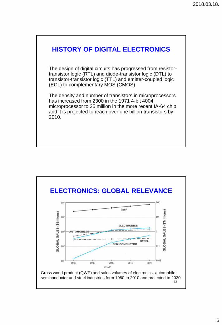
HISTORY OF DIGITAL ELECTRONICS
The design of digital circuits has progressed from resistor-transistor logic (RTL) and diode-transistor logic (DTL) to transistor-transistor logic (TTL) and emitter-coupled logic (ECL) to complementary MOS (CMOS) The density and number of transistors in microprocessors has increased from 2300 in the 1971 4-bit 4004 microprocessor to 25 million in the more recent IA-64 chip and it is projected to reach over one billion transistors by 2010.
12
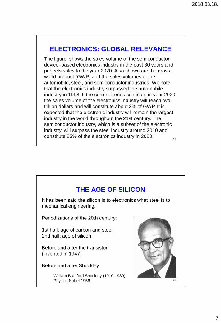
ELECTRONICS: GLOBAL RELEVANCE
Gross world product (QWP) and sales volumes of electronics, automobile,
semiconductor and steel industries form 1980 to 2010 and projected to 2020.
2018.03.18.
7
13
ELECTRONICS: GLOBAL RELEVANCE
The figure shows the sales volume of the semiconductor-
device–based electronics industry in the past 30 years and
projects sales to the year 2020. Also shown are the gross
world product (GWP) and the sales volumes of the
automobile, steel, and semiconductor industries. We note
that the electronics industry surpassed the automobile
industry in 1998. If the current trends continue, in year 2020
the sales volume of the electronics industry will reach two
trillion dollars and will constitute about 3% of GWP. It is
expected that the electronic industry will remain the largest
industry in the world throughout the 21st century. The
semiconductor industry, which is a subset of the electronic
industry, will surpass the steel industry around 2010 and
constitute 25% of the electronics industry in 2020.
14
THE AGE OF SILICON
It has been said the silicon is to electronics what steel is to
mechanical engineering.
Periodizations of the 20th century:
1st half: age of carbon and steel,
2nd half: age of silicon
Before and after the transistor
(invented in 1947)
Before and after Shockley
William Bradford Shockley (1910-1989)
Physics Nobel 1956

2018.03.18.
8
15
MOORE’S LAW
The development of complexity and performance of silicon
devices is unparalelled in the history of technology. Never
before could improvements be measured in terms of
logarithmic scale for such a sustained period. This is often
seen as the embodiment of „Moore’s Law”.
MOORE’S LAW
Gordon Moore (co-founder of Intel) predicted in 1965, just four
years after the first planar integrated circuit was discovered, that
the number of transistors per integrated circuit would double
every 18 months.
He forecast that this trend would continue through 1975.
Moore's Law has been
maintained for far longer,
it has become a universal
law of the entire semi-
conductor industry. It still
holds true as we enter the
second decade of new
century.
Moore’s law is about
human ingenuity not physics.

2018.03.18.
9
MOORE’S LAW
Robert NOYCE the visionary (co-invertor of IC)
Gordon MOORE the virtuoso of technology
Andrew GROVE (GRÓF András) the technologist turned scientist
Logic technology node and transistor gate length versus calendar year.
Note:
mainstream Si technology is nanotechnology.
The INTEL’s gurus: A. Groove, R. Noyce
G. Moore INTEL,1970
18
MOORE’S LAW

2018.03.18.
10
19
FINANCE
Cost (investment) of an IC fab
1999: 5.000.000.000 $
2010: 50.000.000.000 $ = 12.000 billion HUF!
(Hungary’s yearly budget….)
Solution: fabs only at few places …
design at a great lot of places …
CNT
WINDOW INTO THE FUTURE (?):
CNT FET INVERTER AND LOGIC GATES
The first CNTFET circuit: inverter circuit
(red circles : results of five measurement series)

2018.03.18.
11
CNT RING OSCILLATOR
CNT RING OSCILLATOR

2018.03.18.
12
LOGIC CIRCUITS GENERATIONS
AND FAMILIES
The circuit technologies are the relevant factors which
determine and characterize the generations of logic circuits.
A logic family of monolithic digital integrated devices is a
group of electronic logic gates, flip-flops, etc., constructed
using one of several different designs and technology,
usually with compatible logic levels and power supply
characteristic within the family.
Before the widespread use of integrated circuits, various
vacuum-tube and solid-state logic systems were in use, but
these were never as standardized and interoperable as the
IC devices.
LOGIC CIRCUIT GENERATIONS (1)
1930s, relay circuits, Bell Labs
(driving force: telephone exchange switching)
1940s, vacuum tubes e.g. ENIAC, built in 1946 (electronic
numerical integrator and calculator), calculated the trajectory of
an artillery shell in only 30 sec. Large and expensive…
18 thousand vacuum tubes
60 thousand pounds (27 thousand kg)
16200 cubic feet (480 m3)
174 kW
(c.f. four-operation hand-held calculator appr. 9 000 transistors)
(driving force: military applications, artillery shell trajectory
calculations)

2018.03.18.
13
ENIAC: 1946
Further comment: Failure rate of a commercial vacuum tube
is about 1/2000 per hour, of an industrial or high-reliability
type is about 10 times smaller.
Estimated failure rate of the ENIAC about one per hour (!)
26
TRANSISTOR AND IC
Perhaps the invention which determined the 20th century
the greatest manner.
Two transistor concepts:
to control the flow of electrons by external field:
field effect transistor (FET, MOSFET, etc.)
to create inside the material (semiconductor) the
”control electrode”: bipolar junction transistor
FET Field Effect Transistor
MOS Metal-Oxide-Semiconductor
BJT Bipolar Junction Trasistor
TRANSISTOR TRANSfer resISTOR

2018.03.18.
14
LOGIC CIRCUIT GENERATIONS (2) 1950/1960 semiconductor diode and transistor circuits
- RTL resistor-transistor-logic
- DTL diode-transistor-logic
- ECL emitter-coupled logic (later)
From 1961 SSI (above listed on one chip)
1960s TTL (transistor-transistor logic), Sylvania, then Texas
Instruments, the TI system later became the de-facto
industry standard
After 1960/1970: MOS metal oxide semiconductor : pMOS
(1960s) then nMOS (1970s)
1980s CMOS (complementary metal-oxide-semiconductor)
introduced in 1968 by RCA
TRANSISTOR-TRANSISTOR LOGIC:
INTRODUCTION
Mostly widely used IC technologies.
First circuit family: Texas Instruments
Semiconductor Network
74 Series (standard)& 54 Series (military specification)
Combination of BJTs, diodes, and resistors.
Implement logic function, e.g., NAND, NOR, etc.
Package (DIP, SMT)
The TTL system is based on the silicon bipolar transistor
technology. It is a so called „saturation” logic system,
because the transistors are driven to saturation or near-
saturation

2018.03.18.
15
29
TTL: AN INTRODUCTION • One of the commonest IC tecnology (bipolar)
• Two basic version 74 (commercial) and 54 (military)
• Several sub-series
• Bipolar transistors, diodes and resistors
• Packages: DIL, SMT
DIL Dual-In-Line
SMT Surface Mounting Technology
30
Si NPN (PLANAR) TRANSISTOR
n-epi p n +
P-substrate
Electron flow
n +
n+ buried layer
p+ p+
SiO2
Al•Cu•Si Base Collector Emitter
The workhorse of the bipolar ICs is the Si npn transistor

2018.03.18.
16
31
Si NPN (PLANAR) TRANSISTOR
IC: Si BIPOLAR TECHNOLOGY
•Technology optimization: to optimize the Si npn
transistor.
• Components: bipolar transistor, diode, resistor,
capacitor.
• Transistor (and all other components) in-plane structure
– planar technology.

2018.03.18.
17
IC: THE Si BIPOLAR TRANSISTOR
• Typical dimensions:
emitter diffusion (2-2.5) m
base diffusion 4 m
n-epitaxial layer (collector) 10 m
emitter window (small current transistor, ~1 mA)
(10-15) x (10-15) m
E.g. in a TTL circuit one emitter is 16 x 16 m, the nominal
input current is max 1.6 mA (current density 6.25 A/mm2).
34
300 mm (12 in.) ingot and polished silicon wafers

2018.03.18.
18
35 Schematic flow diagram of IC fabrication
36
BURIED LAYER IMPLANTATION
P-silicon
SiO 2
n +

2018.03.18.
19
37
EPITAXY GROWTH
P-silicon
n + buried layer
n-epi
Growth of n-Si epitaxial layer
38
ISOLATION IMPLANTATION
p +
n-epi p +
P-silicon
n + buried layer
P-type implantation (isolation)

2018.03.18.
20
39
EMITTER/COLLECTOR AND BASE
IMPLANTATION
p +
n-epi p +
P-silicon
n + buried layer
p n + n +
Formation of emitter and base regions and of
collector contact region.
40
METAL DEPOSITION AND ETCHING
p + p +
P-silicon
n + buried layer
n-epi
Emitter Base Collector SiO 2
Al•Cu•Si
p + n + n
Deposition of contact and wiring metal layer, and patterning.

2018.03.18.
21
41
PASSIVATION OXIDE DEPOSITION
Emitter Base Collector Al•Cu•Si
CVD oxide
SiO 2
p + p +
P-silicon
n + buried layer
n-epi
p + n + n
IC: THE Si BIPOLAR TRANSISTOR
Region VBE (V) VCE (V) Current
Relation
Cutoff < 0.6 Open
circuit
IB=IC=0
Active 0.6-0.7 > 0.8 IC =hFEIB
Saturation 0.7-0.8 0.2 IB ≥IC/hFE
Typical Si npn transistor parameters

2018.03.18.
22
THE (BIPOLAR) TRANSISTOR
Probably no single development of modern physical science
has touched so many people’s lives so directly as has world-
shaking invention of the transistor.
Xmas 1947: Bell scientists realized the world’s first
successful solid-state amplifier.
The transistor revolutionized electronic communication
devices, as well as making practical the extensive
development of high-speed, high-capacity computers. In
regard to the latter, an important feature of the transistor is
the low amount of energy required per bit of information
processed and its extremely long operational life.
Its invention was truly a landmark, and it is small wonder that
a Nobel prize of physics was awarded in 1956 to the men
primarily responsible: John Bardeen, Walter Brattain, and
William Shockley.
44
TRANSISTOR STORY: MILESTONES
1925-1928 J. E. Lilienfeld, field effect transistor patents
1947 J. Bardeen, W. H. Brattain (Bell Labs),
point contact transistor (physics Nobel prize1956)
1948 W. Shockley (Bell Labs), pn junction,
bipolar transistor (physics Nobel prize, 1956)
1958-1959 J. Kilby (Texas Instruments)
integrated circuit (physics Nobel prize, 2000)
1958-1961 R. Noyce (Fairchild) integrated circuit
(he did not live long enough for the Nobel prize…)

2018.03.18.
23
45
TRANSISTOR HISTORY
1. Prehistoric times (i.e. BS-Before Shockley)
The first forty years of the twentieth century witnessed the discovery of
quantum mechanics, the photon, electroluminescence, the role of defects
in solids and the properties of metal-semiconductor contacts, all of which
laid the foundation for the technological revolution that was to come.
Quantum theory explained the difference between metals,
semiconductors and insulators in terms of energy band-structure, and
accounted for electron states associated with lattice defects and
impurities. In 1934 Fermi invented pseudopotentials, which were to
become vital for band-structure calculations. Schottky and Mott,
separately described the metal-semiconductor contact in 1938, an
understanding that was to become crucial to devices like MESFETs,
MOSFETs, IMPATTs and charge coupled devices. Semiconductors began
to be used as thyristors and photodetectors and point-contact rectification
was beginning to be understood.
And then there was Shockley...
46
2. History
Modern electronics began with the invention of the transistor at Bell
Telephone Laboratories in Murray Hill, New Jersey by Bardeen, Brattain
and Shockley who were subsequently awarded the Nobel Prize in 1956.
The early transistors were chunky, centimetre-sized single crystals of Ge
with p-n junctions back to back involving both electrons and holes. The
physics of p-n junctions was set out in a classic paper by Shockley in
1949, the first example of what was to become a very fruitful interplay of
physics and device technology. Shockley went on to contemplate
the effect of heterojunctions (1951) and the advent of the junction field-
effect transistor (JFET) (1952), innovations that had to wait a number of
years for crystal-growing techniques to catch up with theory. At present
time, field-effect transistors based on Si have revolutionized electronics
and heterojunctions based on GaAs have found extensive roles in hot-
electron transistors, photodetectors and, of course, in quantum-well
devices.

2018.03.18.
24
THE BIPOLAR TRANSISTOR PATENT
A page from the original patent by W.
Shockley:
CIRCUIT ELEMENT UTILIZING
SEMICONDUCTOR MATERIAL
Filed: June 26, 1948
Published: Sep 25, 1951,
2569347
J. Bardeen, W. H. Brattain, Physical
Review 74, 230 (1948)
Bardeen, Brattain, Shockley: Nobel
prize in physics 1956
48

2018.03.18.
25
THE BIPOLAR TRANSISTOR PATENT
50
1947-48: THE TRANSISTOR
William Bradford
Shockley
(1910-1989)
John Bardeen
(1908-1991)
Walter Houser
Brattain
(1902-1987) The Nobel Prize in Physics 1956: "for their researches on
semiconductors and their discovery of the transistor effect"

2018.03.18.
26
51
THE POINT CONTACT TRANSISTOR:
THE FIRST SEMICONDUCTOR AMPLIFIER
William Bradford SHOCKLEY, John BARDEEN, Walter
Houser BRATTAIN, physics Nobel prize in1956
TRANSISTOR TRANSfer resISTOR
1960: THE Si IC PATENT (FAIRCHILD)
A page from the original patent
by R. Noyce:
SEMICONDUCTOR DEVICE-
AND-LEAD STRUCTURE
Filed: July 2?, 1960
Published: April 25, 1961,
2981877
(Robert Noyce, co-founder of
INTEL)

2018.03.18.
27
INTEGRATED CIRCUIT
Kilby: Physics Nobel Prize 2000
The Nobel Prize in Physics 2000:
"for basic work on information and communication technology”
"for his part in the invention of the integrated circuit”
First germanium and silicon integrated circuits
1958: INTEGRATED CIRCUIT
1958: first integrated circuit (Ge) Jack Kilby, Texas Instruments
Physics Nobel Prize 2000 (shared with Zhores I. Alferov and H.
Kroemer)
2018.03.18.
28
55
THE TTL LOGIC CIRCUIT FAMILY
• Basically a modified/improved version of the diode-
transistor-logic (DTL);
• Small scale integrated (SSI) circuit, short delay times;
• Input: multiemitter-transistor (AND function);
• Output: three versions, push-pull (”totem pole”), open
collector, and tri-state;
• Simplest TTL logic gate: two-input NAND gate;
• Inverting gates (NAND, NOR, NOT) are easier to construct;
and implement than non-inverting circuits.
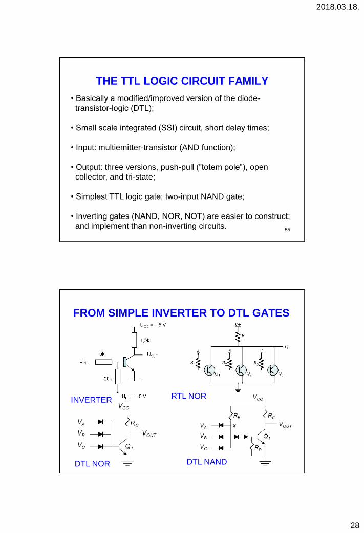
FROM SIMPLE INVERTER TO DTL GATES
56 DTL NOR DTL NAND
INVERTER RTL NOR

2018.03.18.
29
FROM DTL TO TTL ARCHITECTURE
57
58
(BASIC/STANDARD) TTL GATE (NAND)
A
B
D1D2
T2
T1
T4
D3
T3
GND (0V)
VCC (+5V)
Q
&Q
B
A
4 k 1,6 k 130
1 k
• input stage, AND function, T1,
• second stage, phase splitter, T2,
• output inverter stage with active pull-up,
“totem-pole”, T3, T4, with diode level shifter, D3.
• Input diodes would be enough for the logic function,
the transistor effect speeds up the switching.

2018.03.18.
30
59
STANDARD TTL GATE (NAND)
The T4 (upper) transistor of the ”totem-pole” output is an
active pull-up load, resulting in a small dynamic resistance,
facilitating the fast charging up of the capacitors loading the
output, and reducing the
switching time.
The role of the 130 ohm resistor
is the current limitation.
The multiemitter transistor was
patented by Texas Instruments.
The anti-ringing diodes at the input are normally cut off.
During switching transients, they turn on if an input goes
more negative than -0.7V.
60
STANDARD TTL GATE BASIC OPERATION
A
B
D1D2
T2
T1
T4
D3
T3
GND (0V)
VCC (+5V)
Q
&Q
B
A
4 k 1,6 k 130
1 k
If both inputs are HIGH, current through 4k and T1 BC diode
(opens!) will open T2, and T3, then output goes LOW.
If any input is LOW, not enough voltage on the bases of T2
and T3, they are cut-off, output goes HIGH.
A B OUT
1 1 0
X 0 1
0 X 1
NAND

2018.03.18.
31
61
TTL NAND LAYOUT
Circuit diagram of standard 2-
input TTL NAND gate
Layout of twin 4-input TTL
NAND gate
TTL 2x4-INPUT NAND GATE Inputs R1 = 4k R2 =1k
Output R3 = 1.6k R4 = 130ohm
D1
T1
T2
T3
T4

2018.03.18.
32
63
TTL VOLTAGE LEVELS
2V
0,8V
2,4V
0,4V
0V
1V
2V
5V
L
4V
3V
H
Kimeneten: Bemeneten:
T
L
T
H
Output Input
64
STANDARD TTL GATE VOLTAGES:
INPUT LOW
Iin < UT/R1 = 5 V / 4 k 1,2 mA (specification: max 1.6 mA)
Uout (open circuit) = 5 - 2 x 0.7 = +3.6 V
0 V +0.7 V
0 V 0 V +3.6 V (> +2.4 V)

2018.03.18.
33
65
STANDARD TTL GATE VOLTAGES:
INPUT HIGH
+0.7 V
+1.4 V
Uout 0 V (0.4 V)
+2 V
Uin +2 V
~+0.8 V
Iin 40 μA, Uout 0.4 V. T2 and T3 transistors are in
saturation, this is the main speed limiting. 0 1 transition on
output: 10-15 nsec delay. T1 and T2 transistors are in inverse
mode.
66
STANDARD TTL INVERTER
TRANSFER CHARACTERISTICS
Q
0V
1V
2V
5V
4V
3V
1V 2V 3V 4V 5V
U
UA
A Q1
Q = A
The shape of transfer
characterisitcs is determined
by the active pull-up and the
totem-pole output.
In the 0.7-1.4 V input voltage
region T2 transistor operates
as a common emitter
amplifier:
Au = - 1.6 k / 1 k = -1.6
slope: -1.6

2018.03.18.
34
67
OUTPUT STAGE: TOTEM-POLE
Standard TTL circuits: push-pull output
stage: ”totem pole”-output. This is the most
common TTL output. Operation mode:
pull-down and pull-up.
WARNING! TTL totem-pole outputs
cannobe interconnected!
Interconnection of TTL outputs (e.g. bus
system):
open collector output
tri-state output
68
OPEN COLLECTOR OUTPUT
A
D
T2
T1
T3
GND (0V)
VCC (+5V)
QA
Q
1
RT
UT
Ki
The output transistor is operating always in pull-down mode.
If it is ON, it connects the output to ground, if it is OFF, it
separates/disconnects the output (high impedance)
Applications: larger output current, larger supply voltages,
etc., ”wired” logic gates.

2018.03.18.
35
69
SCHMITT-TRIGGER INPUT INVERTER
Q
0V
1V
2V
5V
4V
3V
1V 2V 3V 4V 5V
U
UA
A Q
Q = A
Hiszterézis
0,8 V
Formatting input signals
(speeding up).
Slowly varying, or noisy
signals can be restored
and processed. hysteresis
70
TRI-STATE OUTPUT
A
B
V
Q&
Input V disenables or enables the operation of the gate. If
V is HIGH (disenable) the output goes to a high impedance
state (toward both rail), it is de-facto disconnected.

2018.03.18.
36
71
TRI-STATE OUTPUT
A logic device is always forcing its actual 0 or 1 level to its
output. Both levels but one only at a time.
There is no such thing as three different logic level (signal),
but special elements have a special state, when they are not
forcing any logic signal to their output, but practically release
it, if it were switched off. That is their third state.
Their outputs can be parallel connected, which
is prohibited in case of other gates.
72
TTL TRI-STATE OUTPUT
X1 X2 EN Y
L L H H
L H H H
H L H H
H H H L
irreleváns L leválasztva
Tri-state-output: Modified version of totem-pole output. Zero
level on the ENABLE input drives to cut-off both output
transistor.
irrelevant separated

2018.03.18.
37
TTL PRACTICE: UNUSED INPUTS
The inputs which are not used SHOULD NOT left just
hanging freely! (Because of noise sensitivity).
Not used inputs should be connected to supply or ground
line as appropriate through a resistor of a few kohms.
Unused inputs: (a) connected to another input, (b) NAND
pulled up, (c) NOR pulled down.
74
TTL PRACTICE: TYPICAL PIN-OUTS

2018.03.18.
38
75
TTL PRACTICE: IC PACKAGES
76
TTL PRACTICE: NOISE MARGINS
• Noise margin is the difference between the worst case
output voltage of a stage and the worst case input voltage of
the following stage.
• As larger is the noise margin, as larger is the noise voltage
which when added to the signal does not cause erroneous
operation.
2018.03.18.
39
77
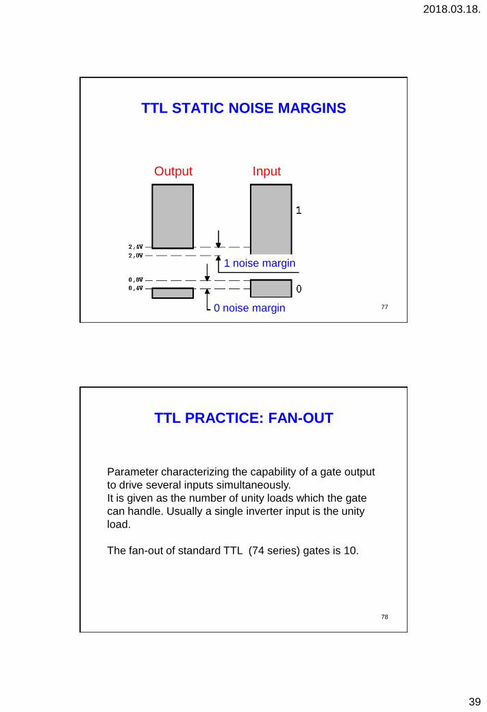
TTL STATIC NOISE MARGINS
Output Input
1 noise margin
0 noise margin
78
TTL PRACTICE: FAN-OUT
Parameter characterizing the capability of a gate output
to drive several inputs simultaneously.
It is given as the number of unity loads which the gate
can handle. Usually a single inverter input is the unity
load.
The fan-out of standard TTL (74 series) gates is 10.

2018.03.18.
40
79
TTL PRACTICE: POWER DISSIPATION
Static:
Ohmic losses (mostly the passive components)
Dynamic:
Ohmic losses (dissipation) during charging and
discharging of the (stray) capacitances through resistors.
In standard TTL (74 series) because of the dynamic
losses, at typical clock rates the dissipation is about 20 %
higher than in static mode.
POWER-DELAY PRODUCT
”Good” circuit: small delay and small power dissipation.
Figure-of-merit: the product of these two parameters
(power-delay product).
Standard 54/74 series: tpd = 10 nsec, P = 10 mW/gate
P tpd = 100 pJ
Interpretation: approximately the energy needed to change
the value of 1 bit.

2018.03.18.
41
LOGIC FAMILY TRADEOFF
81
Propagation delay vs power dissipation for representative
logic families.
82
REVIEW QUESTIONS
1. What do you understand by the term logic family? What is
the significance of the logic family with reference to digital
integrated circuits (ICs)?
2. What is noise immunity? What is propagation delay?
3. Briefly describe propagation delay, power dissipation,
speed–power product, fan-out and noise margin parameters,
with particular reference to their significance as regards the
suitability of the logic family for a given application.
4. What is a multiple emitter transistor?

2018.03.18.
42
83
REVIEW QUESTIONS
5. Compare the standard TTL, low-power Schottky TTL and
Schottky TTL on the basis of speed, power dissipation and
fan-out capability.
6. What is the totem-pole output stage? What are its
advantages?
7. What is the function of the diode at output stage of a totem
pole output configuration
84
PROBLEMS AND EXERCISES
1. The data sheet of a quad two-input AND gate (type
74S08) specifies the propagation delay and power supply
parameters as VCC =5.0V (typical), ICCH (for all four
gates)=18 mA, ICCL (for all four gates)=32 mA, tpLH= 4.5
ns and tpHL =5.0 ns. Determine the speed–power
product specification.
148.4 pJ
2. How many inputs of a low-power Schottky TTL NAND
can be reliably driven from a single output of a Schottky
TTL NAND, given the following relevant specifications for
the devices of two TTL subfamilies:
Schottky TTL: IOH =1.0 mA; IIH= 0.05 mA; IOL =20.0 mA;
IIL =2.0mA
Low-power Schottky TTL: IOH =0.4 mA; IIH= 0.02 mA;
IOL =8.0 mA; IIL =0.4mA