Embed Size (px)
Citation preview

Digital Radio SeminarDigital Radio SeminarAM HD Radio
Jeff WeltonJeff WeltonRegional Sales Manager Regional Sales Manager –– Central U.S.Central U.S.WBA B d t ’ Cli iWBA B d t ’ Cli iWBA Broadcasters’ ClinicWBA Broadcasters’ ClinicMadison, WI October 2008Madison, WI October 2008
© Nautel Limited 2006This presentation has been produced for Nautel customers and agents and is not for distribution without the express written consent of Nautel.
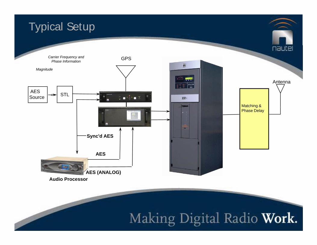
Typical Setup
Magnitude
Carrier Frequency andPhase Information GPS
Antenna
STLAESSource
Matching &
Sync'd AES
atc g &Phase Delay
AES
y
AES (ANALOG)Audio Processor

Transmitter RF Load Requirements
Step 1 – Determine the RF load characteristics
• What does the antenna plot look like?• What does this load look like to the RF amplifiers?What does this load look like to the RF amplifiers?• What is the delay between the antenna and RF amplifiers?
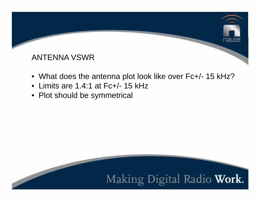
ANTENNA VSWR
• What does the antenna plot look like over Fc+/- 15 kHz?• Limits are 1.4:1 at Fc+/- 15 kHzLimits are 1.4:1 at Fc / 15 kHz• Plot should be symmetrical

Antenna VSWR
Smith Chart h i 1 4 1showing 1.4:1
VSWR Circle

1.4:1 VSWR
Smith Chart showing S t i l l da Symmetrical load
plot.
This is ideal load for amplifiers….not necessarily the same for the output of thefor the output of the transmitter!

Delay through the Transmitter
• How do we determine delay through the transmitter?• Nautel WEB site – www.nautel.comNautel WEB site www.nautel.com• Measure actual delay

www.nautel.com
Marketing 2006 g

www.nautel.com

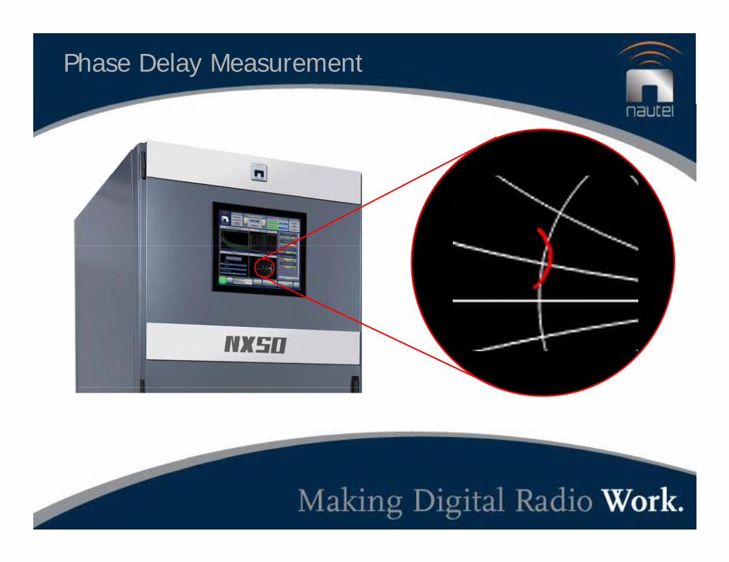
Phase Delay Measurement
PA VOLTSC2
E1
C40.01
5J1
Q52N4401R3
15K####R4
R5
CR5
# RF ALARM ?
C20.047
BROWN3T
Q1STW14NM50
T1
PA VOLTSSAMPLE
RF (1)C51.0
E2
7J12W
R533K
1000R6
1000R7
CR1MUR460
RF DRIVE
1 J1
3 J1
2 J1
4 J1
6 J1
47.5R1
1 5
U1:A
C30.47
15W2.5R2
GREEN
RED3T
YELLOW 2T
ORANGE 2T
Q3STW14NM50
Q2STW14NM50 C6
1.0CR2MUR460
CR3MUR460
+15VC11.0
F11A
SLOW
9 J1
8 J1
10 J1 GREEN3T
BLUE3T
4GND
2GND3 Vs U1:BMIC4452CT
Q4STW14NM50
RF (2)E3
CR4MUR460
JOB07\PA\197\1056S-A SHEET 1 OF 1 VD
Measure output of RF amplifier and transmitter RF output

Phase Delay Measurement
RF Amplifer Voltage
Rf OutputRf Output

Phase Delay Correction
Smith Chart showing S t i l l da Symmetrical load
plot. Let’s assume this load characteristic at the transmitter RF Output
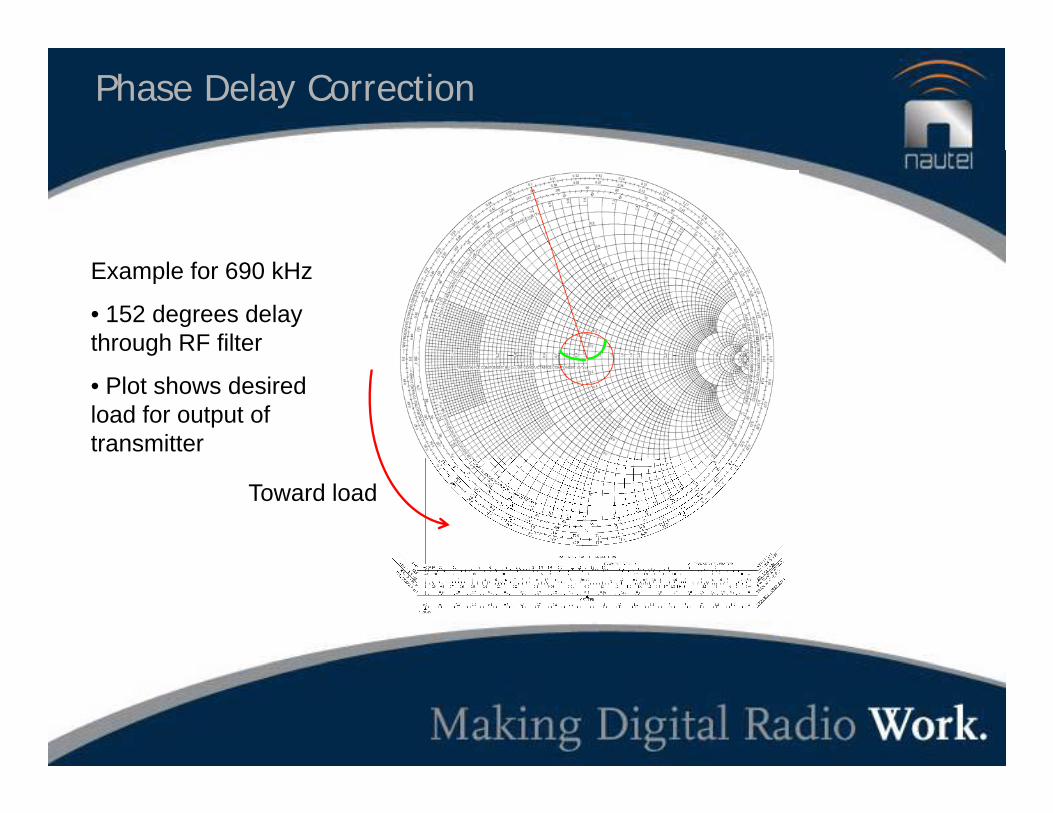
Phase Delay Correction
Example for 690 kHz
• 152 degrees delay through RF filterg
• Plot shows desired load for output of transmitter
Toward load

Phase Delay Measurement
Toward load
Example for 690 kHz
• 28 degrees required between qdesired and current antenna plot
Phase Delay Measurement
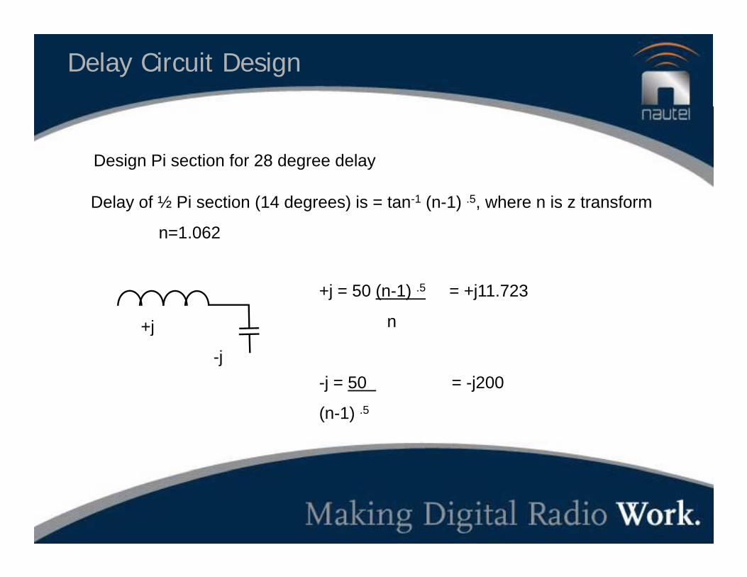
Delay Circuit Design
Design Pi section for 28 degree delay
Delay of ½ Pi section (14 degrees) is = tan-1 (n-1) .5, where n is z transform
n=1.062
+j
+j = 50 (n-1) .5 = +j11.723
n+j
-j
n
-j = 50 = -j200
(n-1) .5

Delay Circuit Design
Design Pi section for 28 degree delay
Complete Pi with two LC sections
5 408uH
+j 11.723 * 2 = +j 23.446 = 5.408 uH @ 690 kHz
-j200 = 1149 pF @ 690 kHz5.408uH j200 1149 pF @ 690 kHz
1149 pF 1149 pF
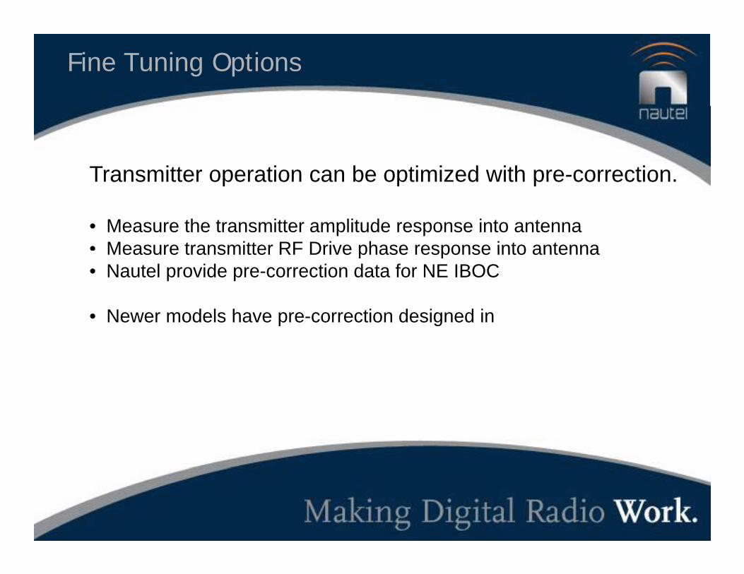
Fine Tuning Options
Transmitter operation can be optimized with pre-correctionTransmitter operation can be optimized with pre correction.
• Measure the transmitter amplitude response into antenna• Measure transmitter RF Drive phase response into antennaMeasure transmitter RF Drive phase response into antenna• Nautel provide pre-correction data for NE IBOC
• Newer models have pre-correction designed inp g

Optimize performance
Transmitter amplitude d i t 50response measured into 50
ohm load
Pre-correction response createdcreated

Transmitter Phase response measured into 50 ohm loadmeasured into 50 ohm load
Pre-correction response created

Spectrum shows excellent reduction in Intermodulation re-growthgrowth

Antenna optimization
Transmitter amplitude d i tresponse measured into
antenna
Pre-correction response createdcreated
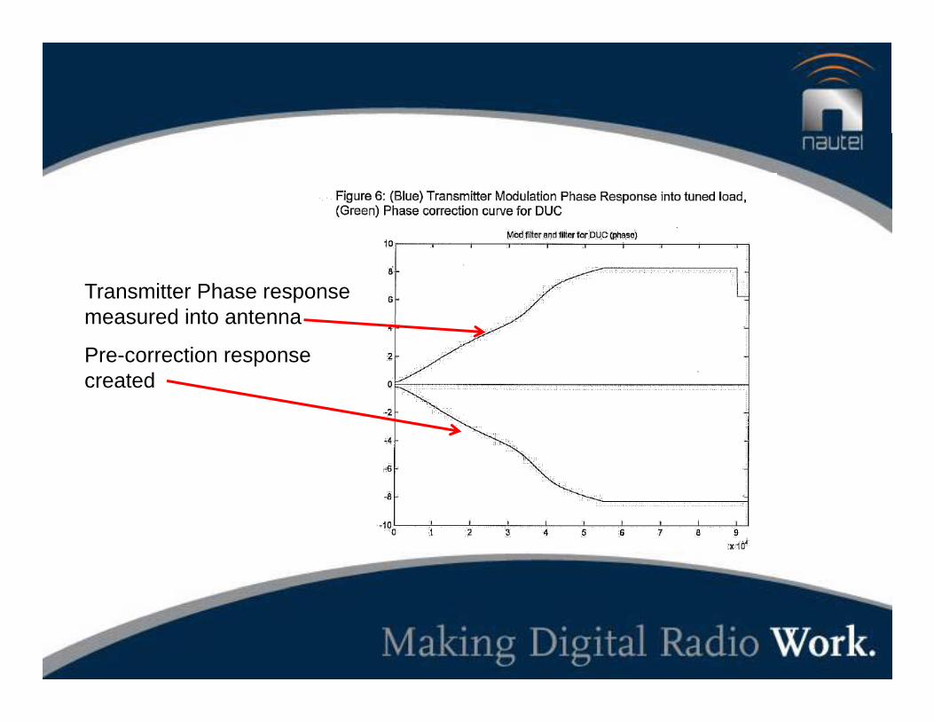
Transmitter Phase response measured into antennameasured into antenna
Pre-correction response created

Spectrum of transmitterSpectrum of transmitter into antenna model at Nautel showing a good margin of safety with
f t threference to the emissions mask

On Air Performance
Spectrum of transmitterSpectrum of transmitter into actual antenna showing a satisfactory margin of safety with
f t threference to the emissions mask
Spectrum using loop antennap g p

FPGA Block Diagram
ateEqualizer B+ 9 Phase PDMAM/AMI Q to Mag 8x FIR 32x CIC
9 PDMGaq
FIR – 64 Tap Comp Generator
I,Q Ref310 kSPS
Correctione I Q t M AM/PM M Ph
I,Q to Mag Interpolator Interpolator
256 I t RF Ph M d l t d
9 PDM 317
MSPSG
ate I,Q to Mag
PhaseAM/PM
CorrectionMag Phase
To I RF DAC
Carrier FrequencyComplex Oscillator
256x InterpFIR/CIC
RF Phase Modulated Carrier 79.4 MSPS
ReflectedPowerSense
2fc IIRFilter
High RFCurrentSenseG
ate256x Decimate
FIR/CICScale &Phase
Correction
RF ADCCombiner Current
Combiner Current310 kSPS
2fc IIRFilter
Sense
Gat
e256x DecimateFIR/CIC
Correction
RF ADCCombiner Voltage
Combiner Voltage310 kSPS
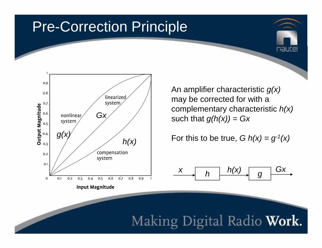
Pre-Correction Principle
An amplifier characteristic g(x)may be corrected for with a complementary characteristic h(x)complementary characteristic h(x)such that g(h(x)) = Gx
For this to be true G h(x) = g-1(x)g(x)h( )
Gx
For this to be true, G h(x) g (x)h(x)
hx Gxh(x)h gx Gxh(x)

Pre-Correction Features
The FPGA has three correction sections in the forward path:
Envelope equalization: Corrects for filtering effects in the modulator (envelope magnitude and phase response versus frequency)
AM/AM Correction: Corrects for amplitude error inAM/AM Correction: Corrects for amplitude error in the modulator due to capacitive effects in the FET. (Essentially AM distortion)
AM/PM Correction: Corrects for phase error in the pRF amplifier due to capacitive effects in the RF FET. (IQM or IPM effects)
Additionally it will be possible to correct for linear effects in the AM antenna system using a filter in the DSP

Typical Correction Curves AM/AM
Gai
n
Envelope Voltage
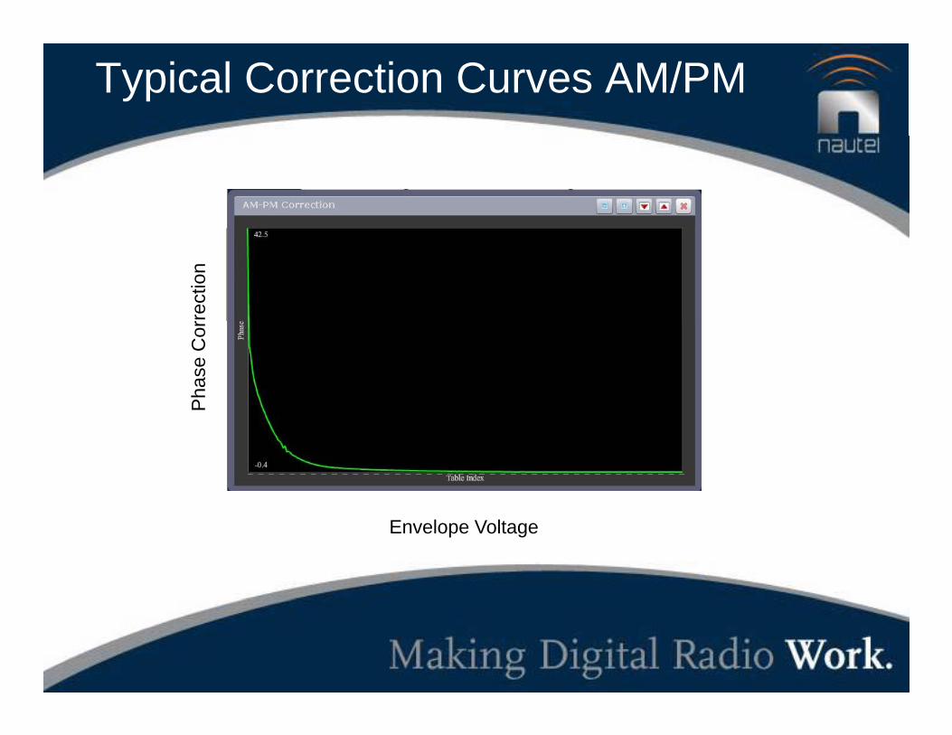
Typical Correction Curves AM/PM
rrec
tion
Pha
se C
or
Envelope Voltage

Conclusions
• A fundamental requirement to broadcast the HD Radio signal is to present a symmetrical load to the RFsignal is to present a symmetrical load to the RF amplifiers with Hermitian symmetry.
• A further improvement to the system linearity can be p y ymade by providing correction data curves for the transmitter amplitude and phase responses.
• Technology improvements are making measurement• Technology improvements are making measurement much simpler on the transmitter end, reducing test equipment requirements and making optimization easier.
• Improvements in pre-correction can also help.