Embed Size (px)
Citation preview
DIGITAL OSCILLOSCOPE AND HIGH SPEED ANALOG CONVERSION
CARD FOR THE DE2 DEVELOPMENT KIT
A Design Project Report
Presented to the Engineering Division of the Graduate School
of Cornell University
in Partial Fulfillment of the Requirements for the Degree of
Master of Engineering (Electrical)
by
Adam Walter Hart
Project Advisor: Bruce Land
Degree Date: August 2008

Abstract
Master of Electrical Engineering Program
Cornell University
Design Project Report
Project Title: Digital Oscilloscope and High Speed Analog Conversion Card for the DE2 Development Kit
Author: Adam Hart
Abstract: This project covers the development of a hardware and software solution to high speed
analog signal generation and capture on the DE2 FPGA board. The hardware portion consists of
a daughter card for the DE2 that houses a digital-to-analog and an analog-to-digital converter
and interfaces with the motherboard’s Cyclone II FPGA. The software portion consists of
Verilog code that implements an oscilloscope and function generator in the FPGA. The
oscilloscope and generator can be configured to operate in different modes. The project was
successful in achieving the desired functionality at acceptable rates of operation, but
performance was limited by design decisions and the simplicity of the approach taken.
Report Approved byProject Advisor: ______________________________________Date: _______________
2
Executive Summary
FPGA technology is a growing field in electrical engineering. Classes at Cornell University
teach the basics of the system, but lack tools to explore certain applications. This project involved the
development of an academic tool to enable the manipulation and investigation of high speed signals.
The goal of the project was to create a bi-directional hardware interface that fed analog values
from the outside world into a processor that displayed them on a screen and that created analog values
to be transmitted to the outside world. This was realized by a circuit board that housed digital-to-
analog and an analog-to-digital conversion chips and an FPGA application that exercised those external
interfaces, and displayed the input channel on a VGA monitor.
The hardware design process involved making decisions about how many data to capture and
create and how they should be processed when they were in analog form. The software design process
involved making decisions about how to store the data and how to perform the digital processing.
Small data sizes were chosen to keep the system simple, and data were stored in a cheap static form for
display and a more expensive, easily manipulated form during acquisition. Analog processing was kept
to a minimum for reliability reasons, and digital processing was performed by logic elements rather
than by a fully architected CPU.
The hardware design was divided into two easily separable parts by data direction. The design
was largely straightforward, but schematic errors prevented it from being as versatile or robust as it was
intended to be. Software design was more complicated because the several systems were required to
interact. Each software module handled the operation of part of the system, but the control scheme
required that they monitor each other for timing and configuration information.
The outcome of the project was a success. The desired functionality was implemented in full,
and could be accurately demonstrated at speeds up to 2MHz. Attempts to achieve higher levels of
performance were made difficult by the structure of the design. Future projects will be able to make
good use of the results of this one.3

Introduction
Field-Programmable-Gate-Array (FPGA) technology allows engineers a great deal of flexibility
in design. The ability to compress large designs into a single chip without investing the time and
money required to create a custom integrated circuit greatly simplifies the design process. Even more
important is the ability to redesign, add functionality and debug in a matter of hours instead of weeks.
FPGAs have gained footing in a wide variety of applications and it important that electrical engineering
students gain experience with the technology.
The Terasic DE2 FPGA development kit is used in classes at Cornell University as a platform
for learning about basic logic and about FPGA capabilities. The DE2 board is capable of a wide range
of functionality, but lacks generic, high-speed digital-to-analog (DAC) and analog-to-digital (ADC)
converters. The closest on-board options are the Audio Codec and the VGA output. The codec is
limited by a maximum sampling rate of 96kHz, which is far below the FPGA's clock of 50MHz. The
VGA output is capable of running at 50MHz but only offers DAC functionality, and is obviously not
available if a particular design uses a VGA screen.
To enable the addition of new functionality to the DE2 board, Terasic provides a pair of expansion
headers. These two ports each make 36 general-purpose-input/output (GPIO) pins from the FPGA, as
well as 3.3V, 5V and Ground power rails available on a standard 100mil header. The FPGA directly
controls the GPIO lines, allowing the end user a great deal of flexibility in connecting new components.
It is important to note that the Terasic expansion headers do not conform to the Altera Santa Cruz
connector form factor and that designs that use the headers will only be usable with DE model boards.
The purpose of this project was to develop DAC and ADC interfaces for the board. These
interfaces were created on a daughter card that connects to the expansion headers on the DE2. Coaxial
cable sockets connect the interfaces to external signal sources and destinations. An FPGA based
oscilloscope application was written to demonstrate the capabilities of the input and output signal
paths.4
Design Requirements
The customer for this project is Dr. Bruce Land. He will use the hardware and software
developed as an aid in teaching ECE 5760. It offers a starting point for exploring high speed DAC and
ADC in a classroom setting. It is considered modifiable even in its final state, as the needs of the
classroom dictate. The malleable nature of FPGA firmware dictates that the easiest changes will be
new applications for the hardware, but the hardware itself may be adapted to new needs. For these
reasons, the software for the oscilloscope shall be written in Verilog for Altera's Quartus II development
environment. Cornell owns licenses for the software in the Phillips Hall Digital Lab, and trial versions
are available at no cost from Altera. The hardware shall be designed using the gEDA suite of
Electronic Design Automation tools. These tools are open source and are available for the Linux
operating system free of charge. All hardware and software created in the course of the project shall be
delivered to Bruce Land on completion.
Functional project requirements can be divided between the hardware and software
components. Hardware shall consist of a daughter card that connects to the DE2 board's expansion
headers. It shall host two signal paths, one DAC and one ADC. Each signal path shall offer a selection
between a direct path on the analog side, or an amplification stage. The converters shall support
positive voltage values only, to simplify the design. The analog side of the daughter card shall feature
industry standard BNC terminals to allow the connection of typical oscilloscope probes.
Software shall consist of a digital oscilloscope and function generator implemented on the
DE2's Cyclone II FPGA. The oscilloscope shall have user settable parameters, including trigger value,
trigger position, and seconds per on-screen division. The oscilloscope output shall be displayed on a
VGA computer screen. The screen shall feature indications of the current parameters, as well as static
line elements that provide spatial reference on the display.
The function generator shall have three user selectable output modes: sine wave, square wave
and triangle wave. The frequency output shall be set by the user between 0 and 16MHz. The 5

amplitude of the output shall be user selectable as a percentage of the maximum range. The state of the
generator shall be displayed on the DE2 board.
Performance requirements were left purposefully vague. Part of the intent of the project was to
test what could be done and explore the possible solutions to the problem. With that in mind, the
requirements feature the establishment of various performance metrics, rather than dictating minimums
that must be met. The ADC and DAC resolution of 8 to 16-bits shall be investigated, and the best
option selected. The ADC and DAC shall have a parallel data bus to allow maximum throughput. The
ADC and DAC integrated circuits shall support an update rate of at least 50MHz. The oscilloscope and
function generator applications shall be exercised across a range of data rates to establish the maximum
stable data rates. The VGA screen shall have a resolution of 640x480 pixels.
Possible Solutions
The needs and purpose of the project determined several important aspects of the design. The
platform was fixed as the DE2 board. This fixed the required shape and layout of the daughter card and
the capabilities of the FPGA that would be used. The capacity of the FPGA was a critical constraint,
because that determined how easy it was to fit a particular design into the chip's logic. The Cyclone II
is not the most expansive FPGA, and large designs or designs with large, logically unwieldy
components may be difficult for the software to fit.
The one of the most important trade offs was the size of the data bus for the ADC and DAC. 1-
bit to 24-bits parallel buses are available, but most applications call for a width between 8 and 16-bits.
The low end of the scale offers shorter settling times and simplicity, while the high end offers
significantly better precision. On the hardware side of the issue, the system was specified as a one
sided supply voltage, and priority was placed on finding converters that were specifically intended for
such functionality. This implied a simpler unit without a differential analog configuration. On the
software side, the oscilloscope must store at least one screen's worth of captured analog values in order 6
to display them for the VGA. This means that wider data buses will take up more FPGA register space
than smaller buses and more logic resources will be required to manipulate them. Since the Cyclone II
is not a large FPGA, a smaller bus width would be preferable. With these considerations in mind,
several ICs were examined, and an 8 bit, single sided ADC and an equivalent DAC were selected.
The other significant hardware trade off was how to structure the analog signal paths. Adding
amplification stages can add flexibility to a design, but also increases the complexity and the number of
points of failure in this untested design. A direct connection avoids these pitfalls, but offers no way to
manipulate the signals in analog space. Filtering was not considered, as digital filters can be
implemented in the FPGA. The solution chosen was to provide both a direct path and an amplified
path for each converter. The user can select between them by switching a set of jumpers. This
approach combines the benefits of analog manipulation with a backup direct path at little extra design
time cost.
The main software design decision was where to put the stored values for display on the FPGA.
The Cyclone II FPGA has both internal registers and RAM units as well as a large external RAM.
Typical VGA applications use the external ram to store a screen's worth of information, as there is not
enough internal memory for a 640x480, 8-bit deep matrix. In this case, however, only one 640-element
line of 8-bit values was needed. The stored values correspond not to pixel intensity, but to the
magnitude of the voltage at each screen column and which row pixel should be lit. Other on screen
elements, such as time and voltage divisions, can be procedurally generated rather than stored. This
permits the use of a large array register or of internal memory to store the signal data. Initial tests
indicated that the large register constructs were expensive in terms of logic, but allowed fast parallel
manipulation and simple programming. Memory, on the other hand, was placed in reserved space on
the chip and was easy to synthesize, but could only be read or written once per cycle. Both techniques
were eventually used in the final design. A register array was created to read in the ADC values and
allow them to be shuffled all at once while the input waited to be triggered. A memory array was
7
created to allow the VGA controller to use a static copy of the last triggered sequence while a new one
was created.
The other major software choice was whether or not to use a NIOS II central processing unit
element in the design. The NIOS II is an automatically generated CPU that Altera provides for use
with its FPGAs. It allows the user to combine pure C software functionality with the firmware written
in Verilog. The programmer can take advantage of the abstraction and sequential execution offered by
the C programming language. The disadvantages include the complexity of adding a second
programming language and set of source files, and the extra space that the CPU core takes up in the
FPGA. It was eventually deemed best to not use the NIOS II. The oscilloscope functionality was not
complex enough to warrant the abstraction of the C language, and the default license of the Quartus
development environment did not include use of the core. It is possible that a proper license could
have been obtained, but time constraints did not permit such delay.
Design
Converters
The design of the daughter card can be broken down by data direction. The DAC is the output
and the ADC is the input. The core of each path is an 8-bit converter chip. 8-bits of precision create a
quantization range of 0.013V when referenced to 3.3V. As described above, this is sufficient for the
purposes of this project. A wide range of integrated circuits supports this precision, offering many
possible configurations. The chips that were selected had interfaces that were uncomplicated by
optional features and nonessential functionality. They were also selected for their high speed
capabilities, achieving at least 50MHz operation. The DAC chip is the HI3338 by Intersil. The ADC
chip is the ADC08100 by National Semiconductor. The two chips operate at different voltages (5V for
the DAC and 3.3V for the ADC), but both analog segments are referenced based on 3.3V. The analog
power pins are fed by a signal that has passed through a low pass filter made up of simple inductor 8

choke. This helps isolate the analog components from digital noise. Both the analog and digital sides
of the system share the same ground. See Appendix B for schematic images and Appendix C for layout
images.
DAC
The DAC is made of two parts, the digital section and the analog section. The digital part
consists of the converter chip, its various support capacitors, and its connection off board. The chip is a
no-frills digital-to-analog converter that operates at a maximum update rate of 50MHz. It needs bypass
capacitors at each of its power pins, but no additional support hardware. The 8 data bits and two
control pins are connected to the FPGA via the low-numbered pins of the JP1 header. The control pins
are LE, which is a conversion enable pin, and COMP, which activates 2's compliment conversion.
The analog part consists of a set of reference voltages, and the analog line to the output
connector. The high reference voltage is set to 3.3V, and the low voltage is set to ground. These values
were chosen to keep the DAC's output voltage ranges compatible with the ADC's input voltages and to
eliminate the need to generate negative voltages. The analog line splits into two signal paths. The user
can select between the two paths by setting the jumpers on CONN1 and CONN2. Connecting pins 3
and 2 selects a path that is terminated for 50Ω, but does not have any active elements. Connecting pins
2 and 1 selects a path that includes an opamp with a gain from 1 to 5. The gain is set via a
potentiometer, R4. All of the signal traces for the analog line are routed such that they do not need to
change layers or cross traces on other layers. The analog output is a right-angle 50Ω BNC connector.
It will allow the user to connect oscilloscope probes directly to the daughter card for testing purposes.
ADC
The ADC is also made up of two parts, the digital section and the analog section. The digital
part consists of the converter chip, its various support hardware, and its connection off board. The chip
9
is a no-frills analog-to-digital converter that operates at a maximum update rate of 100MHz. It needs
bypass capacitors at each of its power pins. The 8 data bits and two control pins are connected to the
FPGA via the high-numbered pins of the JP1 header. The control pins are PD, which powers down the
chip, and CLK, which synchronizes the conversions with the DE2's main digital clock. The clock
signal may require series termination near the pin, which is achieved with a resistor.
The analog part consists of a set of reference voltages, and the analog line to the output
connector. The high reference voltage is based on 3.3V, but is divided down to 2V to keep the current
through the reference resistor ladder within electrical tolerances. The low voltage is set to ground.
These values were chosen to eliminate the need to generate negative voltages. The analog line splits
into two signal paths. The user can select between the two paths by setting the jumpers on CONN3 and
CONN4. Connecting pins 3 and 2 selects a straight shot path that does not have any active elements.
Connecting pins 2 and 1 selects a path that includes an opamp with a gain from 1 to 5 and a voltage
divider that can attenuate the signal to 20% of its original value. The gain and attenuation levels are set
via pair of potentiometers, R11 and R15 respectively. These variations allow a broad range of inputs to
be used without damaging the input. The attenuation, particularly, will allow the opamp gain to be held
higher than three. This improves the phase margin in the ADC chip. All of the signal traces for the
analog line are routed such that they do not need to change layers or cross traces on other layers. The
analog input is a right-angle 50Ω BNC connector. It will allow the user to connect oscilloscope probes
directly to the daughter card for testing purposes.
Construction
Constructing the daughter card was not difficult. Solder paste and a toaster oven were used to
fix the surface mount components to the board. This method is particularly time saving compared to
hand soldering each chip, because the surface tension of the molten solder paste lines the pins up on
their pads and ensures a neat connection. The through-hole components were then hand soldered and
10

the entire board was checked for short circuits. These were also cleaned up by hand. Testing the basic
functionality of the board went smoothly. When connected through the direct analog lines, both the
DAC and ADC were capable of processing values. More extensive, high-speed tests were done after
the software was finished. See Appendix D for photos of the finished board.
Two errors were discovered in this phase of the project. The most obvious problem was that the
signal and ground pins of the BNC connectors had been switched. The solution was to flip them to the
back side of the board. This had an unfortunate side effect of preventing the structural pins of the
connector from mating with the board. The connectors are functional, but delicate. The other error
was that the op-amps were not properly configured. They amplify compared to 0Volts, which adds an
undesirable DC component to the signal. The DAC op-amp does not work as expected. It produces a
strange signal when fed with a sine wave. The ADC side does both amplify and attenuate the signal,
but not to the extent hoped. Neither of these problems can be solved with this revision of the board.
As the design files will be available to Bruce, future work can rectify these errors.
Software
The software for this project was written in the Verilog hardware description language. The
template used was the top level module file and pin assignment file provided by Terasic. These files
define a set of signals that control the various components on the DE2 board and connect the signals to
the proper FPGA pins. This allowed the use of the names provided by Terasic to connect programmer
created logic to the external hardware on the DE2 board.
Several project specific signal sets were created. One set interfaces with the VGA controller.
Another controls the function generator. The control logic uses a third set, and the final set holds the
state of the data capture logic. One 640 element, 8-bit unpacked array was created to store the ADC
data values currently being captured. One reset signal was created and attached to SW[0].
The design consists of 6 main components. The scope control component monitors the input
11

keys and updates the parameters of the scope as the user changes them. The data capture component
records the signal on the ADC data bus according to the parameters of the scope. The VGA controller
is a module that handles the timing of the VGA output. The VGA display component selects what to
draw to the screen based on the pixel location requested by the VGA controller. The function generator
component creates a direct digital synthesis (DDS) output signal based on the setting of the on-board
switches and the scope parameters. The parameter display component parses the scope parameters for
display on the DE2’s seven-segment displays.
Control
The scope control component allows the user to set the values of 7 scope parameters. They are
set using the pushbuttons on the board, called KEYs in the template file. KEYs 0 and 1 cycle through
the various settings. KEYs 2 and 3 increment and decrement the currently active setting. The first
setting is the number of seconds per vertical division of the screen. There are six selectable values:
1μs, 10μs, 100μs, 1ms, 10ms, and 100ms. The second setting is the trigger value. This value dictates
the signal value that must be crossed with a positive slope before the scope will display the signal. It
can be set to any integer between 0 and 255. The third setting is the trigger position. This value
determines where on the screen the triggered signal will be centered. If it is set to the left edge of the
screen, only the data points that are captured after the trigger value will be displayed. As the trigger
position moves to the right, more and more data points collected prior to the triggering value will be
visible. The trigger position can be set to any x-coordinate on the screen, between 0 and 639. The
fourth setting is the trigger mode. It determines whether the scope continually captures new values, or
just once. The fifth setting is the source select for the function generator. Three settings are available:
sine wave, square wave and triangle wave. When any value is changed, a flag is set to indicate this to
the other components. The sixth setting is the frequency of the function generator. It can be changed
by 1Hz when SW[16] is off and by 1000Hz when SW[16] is on. The final setting is the amplitude
12

setting. It determines what fraction of the full 8-bit scale the function generator produces. It can be set
between 1 and 1/8 by powers of 1/2. One more control is available. To prevent the scope from
capturing new values, toggle SW[17]. It acts as a run-stop switch without changing the parameter
settings. See Appendix A for the user’s manual.
Capture
The data capture component collects the values generated by the ADC. It runs on the negative
edge of the clock to allow the ADC output enough time to settle before the FPGA samples it. It
consists of a state machine with 5 states. The first state initializes the machine so that it is ready to fill
an array with captured values. The most important job of the state is to convert the number of seconds
per on-screen division into a number of clock cycles between captured values. This ensures that there
are always exactly 640 values captured over the period represented on the screen. Based on a screen
width of 640 pixels and a sampling rate of 50MHz, the formula for calculating the number of cycles to
wait between values is:
10640
000,000,50 ××= DivisionSecondsPerDelayCount
Equation 1: Required Delay Between Samples
This state immediately transitions to the count state. In the count state, the delay counter increments by
one every cycle. If the counter reaches the target, it is reset, and the current value on the ADC output in
stored in the capture array. There are two ways the value can be stored in this state. If the array index
has not yet reached the trigger position, the value is simply placed in the current index and the index is
advanced. The state machine remains in the count state. Once the index reaches the trigger position, a
more complicated operation takes place. If the data value is not high enough to trigger the scope, all of
the values in the capture array are shifted one element to the left, and the new value is placed
immediately behind the trigger position. The state machine remains in the count state. If the trigger
13

value is met or exceeded by the ADC data, the data are stored in the trigger slot of the array, and the
state advances to the triggered state. In the triggered state, the capture array is filled using the same
mechanism as in the pre-trigger position portion of the of the count state. When the whole array is full,
the state machine transitions back to the copy state to prepare the data for display on the VGA.
The copy state waits for a signal that indicates that the capture array has been copied to
memory. That signal is created by a segment of code that runs in sync with the VGA clock instead of
the state machine’s 50MHz clock. When the VGA driver is in vertical sync, this code increments an
index once per cycle. An internal ram module uses the index to update itself from the capture array.
When the update is complete, a flag is set so that the capture logic state machine can transition to the
delay state. The delay state exists to keep the screen from updating too quickly and to enable the use of
the single capture trigger setting. The state machine will pause here for 1/5 of a second, or until the
trigger mode is set to auto-run, whichever happens second.
VGA Driver
The VGA controller is a Verilog module that is provided for the DE2 board by Terasic. It
handles the timing and logic for the VGA output. It provides an x-y pair of pixel coordinates to the
user and expects the color value of that pixel as an input one cycle later. The value is defined as a 10-
bit number for each of red, green, and blue channels of the RGB additive color model. It requires two
supplementary modules to operate. One is a phase-locked-loop that converts an on-board 27MHz clock
to the 25.17 MHz on which the VGA timings are based. The other provides a delayed reset signal that
ensures the VGA controller has enough time to complete its reset. These modules are the only pieces
of code that were not written by the author of this report.
VGA Display
The VGA display component controls what is written to the screen at each pixel. Since the
14

majority of the screen is blank, and the visible elements can be procedurally generated, only a few pixel
values are stored in a VGA memory. This component selects what to draw based on the currently
requested pixel from the VGA controller. It can draw 7 elements. The first two are the trigger value
and position. The trigger value is drawn as a horizontal red line that the signal must cross to be
displayed. The trigger position is drawn as a vertical green line at the x-coordinate of the triggered
value. The next three elements make up the displayed signal. The simplest display method for the
signal would be to print only the captured values. These values are selected from the VGA memory
while the driver is not in a sync state. If the signal transitions faster than one y-pixel per x-pixel,
however, there will be vertical gaps between the points. This is solved by connecting adjacent points
with vertical lines. These vertical lines make up the other two elements in this group. All three of
these elements are printed at maximum white intensity. The final pair of elements is the rule lines.
They are faint white vertical and horizontal lines that divide the screen space into 10 equal segments in
the x-direction and 8 in the y-direction. They make it easier to read the scope signal. See Appendix E
for display photos.
Function Generator
The function generator is a standard direct digital synthesis device. It is configured to
increment a large register each cycle such that the register rolls back to zero with a particular
frequency. The frequency is set in Hz by the appropriate scope parameter. The amplitude of the signal
is scaled based on the amplitude parameter. Three signals are created by the generator. One is a sine
wave. The top 8-bits of the register are indexed into a sine table that generates one sine period each
time the register overflows. The other two signals are a square wave and a triangle wave. Both of
them switch states when the DDS register reaches either its halfway point or 0. The square wave
switches between a 0x00 output and a 0xFF output, and the triangle wave switches between counting
up and counting down.
15

Parameter Display
The parameter display component is the final component, and is what allows the user to make
sense of the scope. For each of the parameters that can be changed, a character representation was
created for the DE2’s seven-segment display. Two modules were developed to implement this. The
hex_char module translates a subset ASCII values or decimal digits into appropriate representations in
seven segments. One of these was instantiated for each of the 8 HEXx output signals. A char_gen
module controls the translators. It takes each of the scope parameters as an input and outputs one
ASCII or decimal value for each of the hex_char instantiations. char_gen has a different display for
each of the 7 parameters. HEX7 and HEX6 always indicate the setting that is being changed, and the
rest of the digits indicate the value. The following table shows the different modes:
Setting HEX7 HEX6 HEX5 HEX4 HEX3 HEX2 HEX1 HEX0Second/Division S d [100s] [10s] [1s] E - [3 or 6]Trigger Value t r H (base16) [16s] [1s]
Trigger Position t P H (base16) [256s] [16s] [1s]Trigger State t S [Auto or oncE]
Source Setting S S [SinE or Squr or tri]Hertz setting H Z [1048576s] [65536s] [4096s] [256s] [16s] [1s]Amp Setting S A 1 / [2, 4, 8]
Table 1: Parameter Display Layout
Testing
The software was more difficult to test than the hardware. Significant reevaluations of how to
accomplish tasks took place, as well as considerable debugging. Initially, two huge registers were used
to store the capture and display versions of the signal array. The display array was the necessary 640
elements long, but the capture array was twice that size with the trigger value in the center. This
allowed the capture logic to be separate from the location of the trigger position. It took approximately
20 minutes for the program to analyze and fit this design into the FPGA. This was prohibitively long
for a system that was still in development. The design was optimized down to a single 640 element
16

capture array with a dynamically determined trigger position, and a memory based display array. This
cut compile time down to a more reasonable 10 minutes.
The other major reevaluation was the location of the parameter display. Initially, it was to be
part of the VGA display. As the system grew more complex, and the number of parameters increased
from 3 to 7, this became difficult to design. A great number of different characters would have to be
created, and would require 35 pixels each to be legible. As the display was developed toward the end
of the project, this time investment was not feasible. The first alternative considered was the LCD
display on the DE2 board. This had the advantage of some internal processing power and pre-made
letter graphics, but carried a large overhead in timing and processing requirements. The solution
chosen was to use the seven-segment displays on the DE2 board. These suffered from limited display
options and a fixed, small number of digits, but offered parallel updates and simple letter graphics.
A problem that surfaced early in the design process was a timing error in the capture logic. The
most logically demanding operation that the state machine performed was a simultaneous shift of 639
8-bit values by 1 array position in a single 50MHz clock cycle. Most times when the system triggered,
there was no problem. However, when the system updated frequently, erroneous values would appear
on the screen often enough to be obvious. After several attempts to revise the logic that was
responsible, Quartus was configured to apply maximum effort to fit the design into the FPGA. Since
the design did not require maximum resources, the additional timing margin reduced the problem,
though it didn’t eliminate it.
The most puzzling debug problem had to do with the VGA timing. Seemingly at random, small
code changes would cause the VGA display to tear and blur or to recover. It is likely that the
complexity of the logic caused timing problems that only appeared under certain fit conditions.
Attempts were made to ease the load on the VGA signals, but ultimately only tweaking random code
segments seemed to fix the problem.
17

Results
The project performed very well overall. The functional requirements were met, with the
system able to transmit and receive analog signals at a variety or rates and shapes. It was able to
display the signals on a VGA screen with no tearing or timing artifacts. Each of the several settings
worked properly, and the parameter display clearly indicated each setting’s state.
The project also established performance numbers for the hardware and software. The function
generator’s DAC output was tested with a real digital oscilloscope to establish maximum rates. Up to
2MHz, the sine output was largely undistorted. It was also fairly accurate, with an error less than 1%
across the range of 0 to 2MHz. Above 4MHz, the distortion became much more apparent. Peak to
peak measures of the frequency were still very close to the expected values, but the shape was no
longer purely sinusoidal. The DDS unit simply progresses too quickly through the sine table, and no
longer hits enough values to make a clean sine wave. The DAC shows no sign of flagging, however,
and produces reasonable square waves at well over 10MHz.
The scope performs adequately, but suffers significantly from a design decision. At low
frequencies it performs very well, accurately capturing sine, square, and triangle waves produced by
the DAC. Its selectable parameters allow the user to modify the trigger settings and to change the
display time base. A single cycle captured across a 1sec wide screen looks much the same as a cycle
captured across a 10μsec wide screen. In between, the signal compresses or expands smoothly as it
changes. There is a small source of error in the time bases, as they are determined by the width of the
screen and the 50MHz system clock. Time is quantized at 20ns, so the 1μs per division setting is not
exact.
This leads into to bigger limitation of the oscilloscope. Since the system was designed to
require one data point per screen x-coordinate, a time resolution of greater than 1μs per division is not
possible. It would capture less than one point per column. This might not have been insurmountable
with extrapolated lines between points, but that would have made the capture or display logic much 18
more complicated. In addition, such a system would not have produced meaningful output at high
frequencies. Theoretically, the system is capable of capturing up to 25MHz before aliasing becomes a
problem, but displaying a correct waveform at near half of the sampling rate would require a
reconstruction filter, which is beyond the scope of this project.
At a resolution of 1μs per division, the oscilloscope can display a sine wave of up to 2MHz
before the peaks and troughs become difficult to distinguish, and a sine wave of up to 4.5MHz before
they become impossible to distinguish.
Conclusion
This project forms a solid foundation for further experimentation with high speed ADC and
DAC on the DE2 board. Aside from some unfortunate but surmountable design errors, the hardware is
an excellent platform for which to develop FPGA applications. It is simple to use and robust against
user error. The software design process brought to light many issues to consider when attempting to
generate and sample high frequency signals. The software itself gives an example of how to create
several systems that interact with and control one another, yet update their status separately. Future
work could include attempts to use higher frequency FPGA clocks to coax more performance out of the
hardware, or software filtering to improve performance without stressing the hardware.
19

Appendix A
User’s Manual
Hardware
The hardware is straightforward to deal with. The first thing to do is remove the plastic shield on
the DE2 board. This allows access the expansion headers. Second, with the DE2 turned off, plug the
receptacles on the daughter card onto the headers on the DE2 so that the BNC connectors hang out into
space. Check to make sure that the receptacles are centered on the headers.
Connect a BNC terminated cable to BNC1 to access the DAC. Connect one to BNC2 to access the
ADC. Be careful not to stress the connectors, because the signal and ground pins are the only thing
holding them down. Also, be aware that oscilloscope probes often have a switch that toggles attenuation
on and off.
To enable the output and input paths, place 100mil jumpers on the four CONN connectors. Placing
them toward the outside edge enables the direct paths, which are most reliable. Placing them toward the
inside of the board enables the amplified paths, which are not fully operational. To adjust the DAC output
gain, turn the potentiometer labeled R4. To adjust the attenuation factor on the ADC, turn R15. To adjust
the input gain for on the ADC, turn R11.
Software
The controls of the oscilloscope and function generator are the four KEYs, SW[17], SW[16] and
SW[1]. SW[1] is a toggleable reset. It brings the scope settings to their default values, but doesn’t clear
the last captured scope trace. SW[17] is Run-Stop. When it is on, the scope retains its settings, but does
not update the screen.
To change the system settings, use the four KEYs. KEY[0] and KEY[1] change which parameter
is being edited. KEY[2] and KEY[3] decrement and increment the parameter respectively. When the
DDS frequency is being set, SW[16] can be turned on to change the increment to 1000Hz. See Table 1 for
the details of the parameter display. 20

Appendix B
Schematic Images
Figure B1: Schematic Overview
Figure B2: DAC Digital Side
21
Figure B3: DAC Analog Side
Figure B4: ADC Digital Side
22

Figure B5: ADC Detail
Figure B6: ADC Analog Side
23
Appendix C
Layout Images
Figure C1: Top Layout
Figure C2: Bottom Layout
24

Appendix D
Board Photos
Figure D1: Top Side of the Assembled Board
Figure D2: Bottom Side of the Assembled Board
25
Appendix E
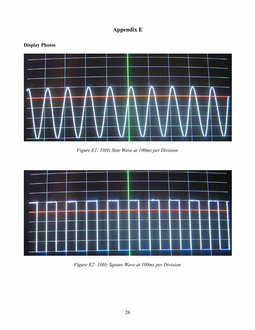
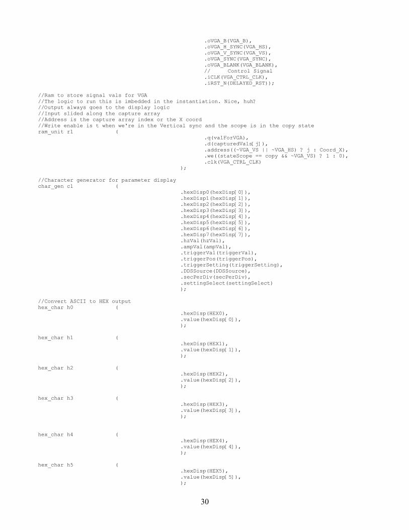
Display Photos
Figure E1: 10Hz Sine Wave at 100ms per Division
Figure E2: 10Hz Square Wave at 100ms per Division
26

Figure E3: 10Hz Triangle Wave at 100ms per Division
Figure E4: 2MHz Sine Wave at 1μs per Division
27

Appendix F
Code
DE2_TOP.v (Header removed for copyright reasons)
//reordered aliases for the DAC and ADC GPIO pinswire [7:0] fastADC;wire [7:0] fastDAC;reg [7:0] oldFastADC;
//Scope control signalsreg [3:0] settingSelect;reg [24:0] controlDelay;reg [2:0] secPerDiv;reg [3:0] DDSSource;reg [23:0] hzVal;reg [3:0] ampVal;reg [7:0] triggerVal;reg [9:0] triggerPos;reg [3:0] triggerSetting;reg newSetting;reg [3:0] stateControl;wire runStop;
//VGA Elementswire DELAYED_RST;wire VGA_CTRL_CLK;wire AUD_CTRL_CLK;wire [9:0] mVGA_R;wire [9:0] mVGA_G;wire [9:0] mVGA_B;wire [19:0] mVGA_ADDR; //video memory addresswire [9:0] Coord_X, Coord_Y; //display coodsreg [3:0] stateVGA;reg [9:0] signalRed;reg [9:0] signalGreen;reg [9:0] signalBlue;reg memTransferDone;
//Scope capture signalsreg [16:0] captureCounter;reg [16:0] counterTarget;reg [10:0] arrayPosition;reg [3:0] stateScope;reg [9:0] i;reg [9:0] j;reg [25:0] updateDelay;
//Display elementswire [7:0] hexDisp [7:0];
//Signal generator elementsreg [7:0] sine;wire [7:0] square;wire [7:0] triangle;wire [7:0] sinAddr;reg [31:0] sinDDS;wire [31:0] ddsInc;wire [7:0] DDSOut;
//Array to hold captured valuesreg [7:0] capturedVals [0:639];wire [7:0] valForVGA;reg [7:0] oldValForVGA;
//Scope statesparameter init=4'd1, count=4'd2, triggered=4'd3, copy=4'd4, delay=5'd5;
//Control statesparameter idleControl=4'd0, delayControl=4'd1;
28

//Setting selectedparameter setSecPerDiv=4'd0, setTriggerVal=4'd1, setTriggerPos=4'd2, setTriggerSetting=4'd3, setSource=4'd4, setHz=4'd5, setAmpVal=4'd6;
//Function generatedparameter makeSine=4'd0, makeSquare=4'd1, makeTriangle=4'd2;
//Triggering modeparameter freeRunning=4'd0, once=4'd1;
// Turn on all displayassign LEDG = {1'h1, fastDAC};assign LEDR = sinDDS[31:14];assign LCD_ON = 1'b1;assign LCD_BLON = 1'b1;
// All inout port turn to tri-stateassign DRAM_DQ = 16'hzzzz;assign FL_DQ = 8'hzz;assign SRAM_DQ = 16'hzzzz;assign OTG_DATA = 16'hzzzz;assign LCD_DATA = 8'hzz;assign SD_DAT = 1'bz;assign I2C_SDAT = 1'bz;assign ENET_DATA = 16'hzzzz;assign AUD_ADCLRCK = 1'bz;assign AUD_DACLRCK = 1'bz;assign AUD_BCLK = 1'bz;assign GPIO_1 = 36'hzzzzzzzzz;assign GPIO_0 = 36'hzzzzzzzzz;
assign TD_RESET = 1'b1; //Enable 27 MHz
assign runStop = (SW[17]);
//set up the GPIO pins to run the daughter cardassign GPIO_0[35:34] = {CLOCK_50, 1'b0};assign fastADC = {GPIO_0[26], GPIO_0[27], GPIO_0[28], GPIO_0[29], GPIO_0[30], GPIO_0[31], GPIO_0[32], GPIO_0[33]};assign GPIO_0[25:10] = 16'hzzzz;assign GPIO_0[9:2] = {fastDAC[0], fastDAC[1], fastDAC[2], fastDAC[3], fastDAC[4], fastDAC[5], fastDAC[6], fastDAC[7]};assign GPIO_0[ 1: 0] = 2'b00;
//Output is the DDS output scaled by Amplitude value assign fastDAC = DDSOut >> ampVal;
//VGA signalsassign mVGA_R = signalRed;assign mVGA_G = signalGreen;assign mVGA_B = signalBlue;
//Signal Gennerator DDS incrementassign ddsInc = (hzVal * 159); //159= 2^32/27000000 so hzVal is in Hz
//For VGA resetReset_Delay r0 ( .iCLK(CLOCK_50),.oRESET(DELAYED_RST));
//For VGA CLKVGA_Audio_PLL p1 (
.areset(~DELAYED_RST),.inclk0(CLOCK_27),.c0(VGA_CTRL_CLK),.c1(AUD_CTRL_CLK),.c2(VGA_CLK));
//For Driving VGAVGA_Controller u1 ( // Host Side
.iCursor_RGB_EN(4'b0111),
.oAddress(mVGA_ADDR),
.oCoord_X(Coord_X),
.oCoord_Y(Coord_Y),
.iRed(mVGA_R),
.iGreen(mVGA_G),
.iBlue(mVGA_B),// VGA Side.oVGA_R(VGA_R),.oVGA_G(VGA_G),
29
.oVGA_B(VGA_B),
.oVGA_H_SYNC(VGA_HS),
.oVGA_V_SYNC(VGA_VS),
.oVGA_SYNC(VGA_SYNC),
.oVGA_BLANK(VGA_BLANK),// Control Signal.iCLK(VGA_CTRL_CLK),.iRST_N(DELAYED_RST));
//Ram to store signal vals for VGA//The logic to run this is imbedded in the instantiation. Nice, huh?//Output always goes to the display logic//Input slided along the capture array//Address is the capture array index or the X coord//Write enable is t when we're in the Vertical sync and the scope is in the copy stateram_unit r1 (
.q(valForVGA),
.d(capturedVals[j]),
.address((~VGA_VS || ~VGA_HS) ? j : Coord_X),
.we((stateScope == copy && ~VGA_VS) ? 1 : 0),
.clk(VGA_CTRL_CLK));
//Character generator for parameter displaychar_gen c1 (
.hexDisp0(hexDisp[0]),
.hexDisp1(hexDisp[1]),
.hexDisp2(hexDisp[2]),
.hexDisp3(hexDisp[3]),
.hexDisp4(hexDisp[4]),
.hexDisp5(hexDisp[5]),
.hexDisp6(hexDisp[6]),
.hexDisp7(hexDisp[7]),
.hzVal(hzVal),
.ampVal(ampVal),
.triggerVal(triggerVal),
.triggerPos(triggerPos),
.triggerSetting(triggerSetting),
.DDSSource(DDSSource),
.secPerDiv(secPerDiv),
.settingSelect(settingSelect));
//Convert ASCII to HEX output hex_char h0 (
.hexDisp(HEX0),
.value(hexDisp[0]),);
hex_char h1 (.hexDisp(HEX1),.value(hexDisp[1]),);
hex_char h2 (.hexDisp(HEX2),.value(hexDisp[2]),);
hex_char h3 (.hexDisp(HEX3),.value(hexDisp[3]),);
hex_char h4 (.hexDisp(HEX4),.value(hexDisp[4]),);
hex_char h5 (.hexDisp(HEX5),.value(hexDisp[5]),);
30

hex_char h6 (.hexDisp(HEX6),.value(hexDisp[6]),);
hex_char h7 (.hexDisp(HEX7),.value(hexDisp[7]),);
//Scope controlalways @ (posedge CLOCK_50)begin
if (~DELAYED_RST || SW[0])begin
triggerVal <= 8'd128;triggerPos <= 10'd320;secPerDiv <= 3'b0;controlDelay <= 25'd0;settingSelect <= 4'b0;newSetting <= 1'b0;hzVal <= 24'h0;ampVal <= 4'h0;triggerSetting <= 4'b0;stateControl <= idleControl;settingSelect <= setSecPerDiv;DDSSource <= 4'b0;
end//no input when stoppedelse if (runStop)begin
stateControl <= idleControl;endelsebegin
//control state machinecase(stateControl)
idleControl:begin
//reset delay valuecontrolDelay <= 25'd0;//if a key 0 or 1 is pressed, change which setting is selectedif (KEY[0] == 0 && settingSelect < 6)begin
settingSelect <= settingSelect + 1;newSetting <= 1;stateControl <= delayControl;
endelse if (KEY[1] == 0 && settingSelect > 0)begin
settingSelect <= settingSelect - 1;newSetting <= 1;stateControl <= delayControl;
endelsebegin
//If key 2 or 3 is pressed, increment or decrement the selected parameter
case(settingSelect)//seconds per divisionsetSecPerDiv:begin
if (KEY[2] == 0 && secPerDiv < 5)begin
secPerDiv <= secPerDiv + 1;newSetting <= 1;stateControl <= delayControl;
endelse if (KEY[3] == 0 && secPerDiv > 0)begin
secPerDiv <= secPerDiv - 1;newSetting <= 1;stateControl <= delayControl;
endend
31
//trigger valuesetTriggerVal:begin
if (KEY[2] == 0 && triggerVal < 255)begin
triggerVal <= triggerVal + 1;newSetting <= 1;controlDelay <= 25'd28000000;stateControl <= delayControl;
endelse if (KEY[3] == 0 && triggerVal > 0)begin
triggerVal <= triggerVal - 1;newSetting <= 1;controlDelay <= 25'd28000000;stateControl <= delayControl;
endend
//trigger positionsetTriggerPos:begin
if (KEY[2] == 0 && triggerPos < 639)begin
triggerPos <= triggerPos + 1;newSetting <= 1;//Don't wait as long between changes of some
parameterscontrolDelay <= 25'd28000000;stateControl <= delayControl;
endelse if (KEY[3] == 0 && triggerPos > 0)begin
triggerPos <= triggerPos - 1;newSetting <= 1;controlDelay <= 25'd28000000;stateControl <= delayControl;
endend
//Trigger modesetTriggerSetting:begin
if (KEY[2] == 0 && triggerSetting < 1)begin
triggerSetting <= triggerSetting + 1;newSetting <= 1;stateControl <= delayControl;
endelse if (KEY[3] == 0 && triggerSetting > 0)begin
triggerSetting <= triggerSetting - 1;newSetting <= 1;stateControl <= delayControl;
endend
//DDS sourcesetSource:begin
if (KEY[2] == 0 && DDSSource < 2)begin
DDSSource <= DDSSource + 1;newSetting <= 1;stateControl <= delayControl;
endelse if (KEY[3] == 0 && DDSSource > 0)begin
DDSSource <= DDSSource - 1;newSetting <= 1;stateControl <= delayControl;
endend
32

//frequency settingsetHz:begin
if (KEY[2] == 0 && ((hzVal < 16000000 && ~SW[16]) || (hzVal < 15999001 && SW[16])))
begin//Change frequency faster when SW 16 is onif (SW[16])begin
hzVal <= hzVal + 1000;controlDelay <= 25'd29500000;
endelsebegin
hzVal <= hzVal + 1;controlDelay <= 25'd29100000;
endnewSetting <= 1;stateControl <= delayControl;
endelse if (KEY[3] == 0 && ((hzVal > 0 && ~SW[16]) ||
(hzVal > 999 && SW[16])))begin
if (SW[16])begin
hzVal <= hzVal - 1000;controlDelay <= 25'd29500000;
endelsebegin
hzVal <= hzVal - 1;controlDelay <= 25'd29100000;
endnewSetting <= 1;stateControl <= delayControl;
endend
//Set amplitude dividersetAmpVal:begin
if (KEY[2] == 0 && ampVal < 3)begin
ampVal <= ampVal + 1;newSetting <= 1;stateControl <= delayControl;
endelse if (KEY[3] == 0 && ampVal > 0)begin
ampVal <= ampVal - 1;newSetting <= 1;stateControl <= delayControl;
endend
default: settingSelect <= setSecPerDiv;endcase
endend
//Wait here to keep settings from being changed too fastdelayControl:begin
newSetting <= 0;if (controlDelay <= 25'd30000000)begin
controlDelay <= controlDelay + 1;stateControl <= delayControl;
endelsebegin
stateControl <= idleControl;end
end
33
default: stateControl <= idleControl;endcase
endend
//VGA displayalways @ (posedge VGA_CTRL_CLK)begin
oldValForVGA <= valForVGA;//display the points that are storedif ((Coord_Y == (360 - valForVGA)))begin
signalRed <= 10'h000;signalBlue <= 10'h3FF;signalGreen <= 10'h000;
end//connect adjacent points with vertical lineselse if (((360 - oldValForVGA) <= Coord_Y) && (Coord_Y <= (360 - valForVGA)))begin
signalRed <= 10'h3FF;signalBlue <= 10'h3FF;signalGreen <= 10'h3FF;
end//connect adjacent points with vertical lineselse if (((360 - oldValForVGA) >= Coord_Y) && (Coord_Y >= (360 - valForVGA)))begin
signalRed <= 10'h3FF;signalBlue <= 10'h3FF;signalGreen <= 10'h3FF;
end//display the trigger value lineelse if (Coord_Y == (360 - triggerVal))begin
signalRed <= 10'h3FF;signalBlue <= 10'h000;signalGreen <= 10'h000;
end//display the trigger position lineelse if (Coord_X == triggerPos)begin
signalRed <= 10'h000;signalBlue <= 10'h000;signalGreen <= 10'h3FF;
end//display the vertical guide lines else if ((Coord_X == 0) || (Coord_X == 64) || (Coord_X == 128) || (Coord_X == 192) || (Coord_X
== 256) || (Coord_X == 320) || (Coord_X == 384) || (Coord_X == 448) || (Coord_X == 512) || (Coord_X == 576))
beginsignalRed <= 10'h0FF;signalBlue <= 10'h0FF;signalGreen <= 10'h0FF;
end//display the horizontal guide lineselse if ((Coord_Y == 360) || (Coord_Y == 328) || (Coord_Y == 296) || (Coord_Y == 264) ||
(Coord_Y == 232) || (Coord_Y == 200) || (Coord_Y == 168) || (Coord_Y == 136) || (Coord_Y == 104))begin
signalRed <= 10'h0FF;signalBlue <= 10'h0FF;signalGreen <= 10'h0FF;
end//Everything else is blackelse begin
signalRed <= 10'h000;signalBlue <= 10'h000;signalGreen <= 10'h000;
endend
//Capture data valuesalways @ (negedge CLOCK_50)begin
if (runStop | newSetting)
34
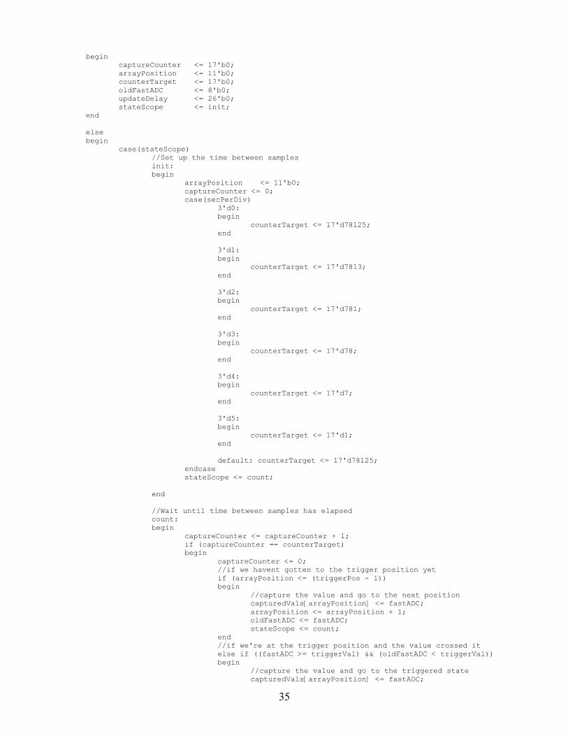
begincaptureCounter <= 17'b0;arrayPosition <= 11'b0;counterTarget <= 17'b0;oldFastADC <= 8'b0;updateDelay <= 26'b0;stateScope <= init;
end
elsebegin
case(stateScope)//Set up the time between samplesinit:begin
arrayPosition <= 11'b0;captureCounter <= 0;case(secPerDiv)
3'd0:begin
counterTarget <= 17'd78125;end
3'd1:begin
counterTarget <= 17'd7813;end
3'd2:begin
counterTarget <= 17'd781;end
3'd3:begin
counterTarget <= 17'd78;end
3'd4:begin
counterTarget <= 17'd7;end
3'd5:begin
counterTarget <= 17'd1;end
default: counterTarget <= 17'd78125;endcasestateScope <= count;
end
//Wait until time between samples has elapsedcount:begin
captureCounter <= captureCounter + 1;if (captureCounter == counterTarget)begin
captureCounter <= 0;//if we havent gotten to the trigger position yetif (arrayPosition <= (triggerPos - 1))begin
//capture the value and go to the next positioncapturedVals[arrayPosition] <= fastADC;arrayPosition <= arrayPosition + 1;oldFastADC <= fastADC;stateScope <= count;
end//if we're at the trigger position and the value crossed itelse if ((fastADC >= triggerVal) && (oldFastADC < triggerVal))begin
//capture the value and go to the triggered statecapturedVals[arrayPosition] <= fastADC;
35
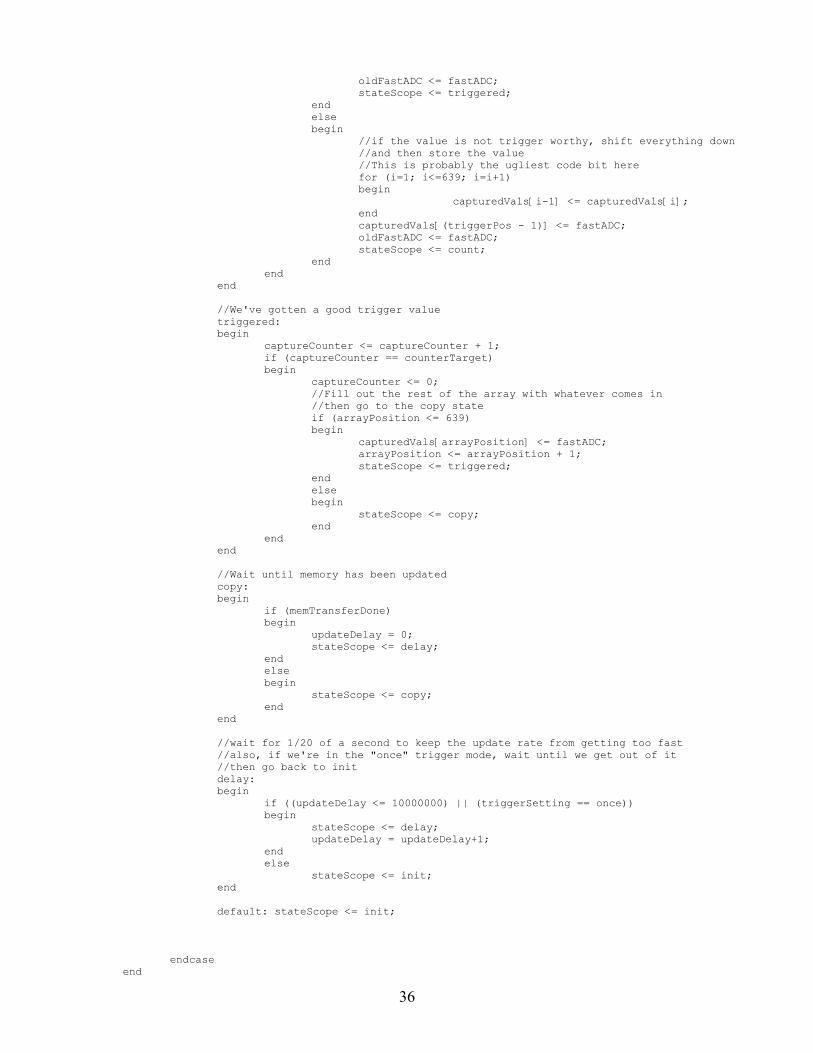
oldFastADC <= fastADC;stateScope <= triggered;
endelsebegin
//if the value is not trigger worthy, shift everything down//and then store the value//This is probably the ugliest code bit herefor (i=1; i<=639; i=i+1)begin
capturedVals[i-1] <= capturedVals[i];endcapturedVals[(triggerPos - 1)] <= fastADC;oldFastADC <= fastADC;stateScope <= count;
endend
end
//We've gotten a good trigger valuetriggered:begin
captureCounter <= captureCounter + 1;if (captureCounter == counterTarget)begin
captureCounter <= 0;//Fill out the rest of the array with whatever comes in//then go to the copy stateif (arrayPosition <= 639)begin
capturedVals[arrayPosition] <= fastADC;arrayPosition <= arrayPosition + 1;stateScope <= triggered;
endelsebegin
stateScope <= copy;end
endend
//Wait until memory has been updatedcopy:begin
if (memTransferDone)begin
updateDelay = 0;stateScope <= delay;
endelsebegin
stateScope <= copy;end
end
//wait for 1/20 of a second to keep the update rate from getting too fast//also, if we're in the "once" trigger mode, wait until we get out of it//then go back to initdelay:begin
if ((updateDelay <= 10000000) || (triggerSetting == once))begin
stateScope <= delay;updateDelay = updateDelay+1;
endelse
stateScope <= init;end
default: stateScope <= init;
endcaseend
36
end
//VGA memory update//needed so the memory ram can run at VGA clock ratealways @ (posedge VGA_CTRL_CLK)begin
if (runStop | newSetting)begin
memTransferDone <= 0;j <= 0;
endelse if (memTransferDone)begin
j <= 0;memTransferDone <= 0;
end//if we're in the scope copy state and it's a Veritcal syncelse if ((stateScope == copy) && (~VGA_VS))begin
if ( j <= 10'd639 )begin
//increment through the screen's x indicesj <= j+1;
end elsebegin
//When we're done, let the copy state knowmemTransferDone <= 1;
endend
end
//DDS updater on CLOCK_27 b/c 50MHz sampling ratealways@(negedge CLOCK_27)begin
sinDDS <= sinDDS + ddsInc ;end
//Sine wave generatorassign sinAddr = sinDDS[31:24];
//Square wave generatorassign square = ((sinDDS[31] == 1) ? 8'hFF : 8'h00);
//Triangle wave generatorassign triangle = ((sinDDS[31] == 1) ? sinDDS[31:24] : 8'hFF - sinDDS[31:24]);
assign DDSOut = (DDSSource == makeSine) ? sine: ((DDSSource == makeTriangle) ? triangle: ((DDSSource == makeSquare) ? square: 0));
//Sin Wave ROM Tablealways@(sinAddr)begin case(sinAddr) 8'h00: sine = 8'hFF ;
8'h01: sine = 8'hFE ;8'h02: sine = 8'hFE ;8'h03: sine = 8'hFE ;.//Values removed to save space..8'hfe: sine = 8'hFE ;8'hff: sine = 8'hFE ;default: sine = 8'h0;
endcaseend
endmodule
37

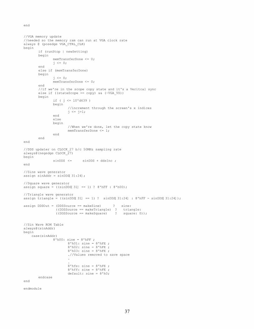
char_gen.vmodule char_gen(
output reg [7:0] hexDisp0,output reg [7:0] hexDisp1,output reg [7:0] hexDisp2,output reg [7:0] hexDisp3,output reg [7:0] hexDisp4,output reg [7:0] hexDisp5,output reg [7:0] hexDisp6,output reg [7:0] hexDisp7,input [23:0] hzVal,input [3:0] ampVal,input [7:0] triggerVal,input [9:0] triggerPos,input [3:0] triggerSetting,input [3:0] DDSSource,input [3:0] secPerDiv,input [3:0] settingSelect);
//Setting selectedparameter setSecPerDiv=4'd0, setTriggerVal=4'd1, setTriggerPos=4'd2, setTriggerSetting=4'd3, setSource=4'd4, setHz=4'd5, setAmpVal=4'd6;
//is a blank b/c no one ever uses ascii 255parameter blank=255;
//when anything changesalways @ (secPerDiv or triggerVal or triggerPos or DDSSource or settingSelect or hzVal or ampVal or triggerSetting) begin
//if it's your state you get to pick what ascii value gets sent to each hex_char//Sec per div is in base 10, everything else is base 16//hexDisp7 and hexDisp7 show the setting, and the rest is the value of the settingif (settingSelect == setSecPerDiv)begin
hexDisp0 <= (secPerDiv > 2) ? 6 : 3;hexDisp1 <= "-";hexDisp2 <= "e";hexDisp3 <= (secPerDiv == 2 || secPerDiv == 5) ? 1 : 0;hexDisp4 <= (secPerDiv == 1 || secPerDiv == 4) ? 1 : 0;hexDisp5 <= (secPerDiv == 0 || secPerDiv == 3) ? 1 : 0;hexDisp6 <= "d";hexDisp7 <= "s";
endelse if (settingSelect == setTriggerVal)begin
hexDisp0 <= triggerVal[3:0];hexDisp1 <= triggerVal[7:4];hexDisp2 <= blank;hexDisp3 <= "h";hexDisp4 <= blank;hexDisp5 <= blank;hexDisp6 <= "r";hexDisp7 <= "t";
endelse if (settingSelect == setTriggerPos)begin
hexDisp0 <= triggerPos[3:0];hexDisp1 <= triggerPos[7:4];hexDisp2 <= {2'b0,triggerPos[9:8]};hexDisp3 <= "h";hexDisp4 <= blank;hexDisp5 <= blank;hexDisp6 <= "p";hexDisp7 <= "t";
endelse if (settingSelect == setTriggerSetting)begin
hexDisp0 <= (triggerSetting == 0) ? "o" : "e";hexDisp1 <= (triggerSetting == 0) ? "t" : "c";hexDisp2 <= (triggerSetting == 0) ? "u" : "n";hexDisp3 <= (triggerSetting == 0) ? "A" : "o";hexDisp4 <= blank;hexDisp5 <= blank;
38

hexDisp6 <= "s";hexDisp7 <= "t";
endelse if (settingSelect == setSource)begin
hexDisp0 <= (DDSSource == 0) ? "e" : (DDSSource == 1) ? "r" : blank;hexDisp1 <= (DDSSource == 0) ? "n" : (DDSSource == 1) ? "u" : "i";hexDisp2 <= (DDSSource == 0) ? "i" : (DDSSource == 1) ? "q" : "r";hexDisp3 <= (DDSSource == 0) ? "s" : (DDSSource == 1) ? "s" : "t";hexDisp4 <= blank;hexDisp5 <= blank;hexDisp6 <= "s";hexDisp7 <= "s";
endelse if (settingSelect == setHz)begin
hexDisp0 <= hzVal[3:0];hexDisp1 <= hzVal[7:4];hexDisp2 <= hzVal[11:8];hexDisp3 <= hzVal[15:12];hexDisp4 <= hzVal[19:16];hexDisp5 <= hzVal[23:20];hexDisp6 <= "z";hexDisp7 <= "h";
endelse if (settingSelect == setAmpVal)begin
hexDisp0 <= (1 << ampVal[3:0]);hexDisp1 <= "/";hexDisp2 <= 1;hexDisp3 <= blank;hexDisp4 <= blank;hexDisp5 <= blank;hexDisp6 <= "A";hexDisp7 <= "s";
endendendmodule
hex_char.vmodule hex_char(
output reg [6:0] hexDisp,input [7:0] value);
parameter blank=255;
//every time the input changes, light the proper seven-segment segmentsalways @ (value) begin
case(value)7'd0:
hexDisp <= 7'b100_0000;7'd1:
hexDisp <= 7'b111_1001;7'd2:
hexDisp <= 7'b010_0100;7'd3:
hexDisp <= 7'b011_0000;7'd4:
hexDisp <= 7'b001_1001;7'd5:
hexDisp <= 7'b001_0010;7'd6:
hexDisp <= 7'b000_0010;7'd7:
hexDisp <= 7'b111_1000;7'd8:
hexDisp <= 7'b000_0000;7'd9:
hexDisp <= 7'b001_0000;7'hA:
hexDisp <= 7'b000_1000;7'hB:
39

hexDisp <= 7'b000_0011;7'hC:
hexDisp <= 7'b100_0110;7'hD:
hexDisp <= 7'b010_0001;7'hE:
hexDisp <= 7'b000_0110;7'hF:
hexDisp <= 7'b000_1110;blank:
hexDisp <= 7'b111_1111;"s":
hexDisp <= 7'b001_0010;"A":
hexDisp <= 7'b000_1000;"i":
hexDisp <= 7'b111_1011;"o":
hexDisp <= 7'b010_0011;"t":
hexDisp <= 7'b000_0111;"m":
hexDisp <= 7'b000_0110;"n":
hexDisp <= 7'b010_1011;"c":
hexDisp <= 7'b010_0111;"-":
hexDisp <= 7'b011_1111;"e":
hexDisp <= 7'b000_0110;"h":
hexDisp <= 7'b000_1001;"z":
hexDisp <= 7'b010_0100;"d":
hexDisp <= 7'b010_0001;"q":
hexDisp <= 7'b001_1000;"/":
hexDisp <= 7'b010_1101;"r":
hexDisp <= 7'b010_1111;"p":
hexDisp <= 7'b000_1100;"u":
hexDisp <= 7'b110_0011;
default: hexDisp <= 7'b111_1111;
endcaseendendmodule
40