Embed Size (px)
Citation preview
Handout for Digital Logic Design (ECEG3201) 3rd year (Regular), 2003E.C
Chapter 1 Introduction to digital logic design
Introduction
I started studying digital electronics in the first months of year 1989; at that time I wanted to build digitally controlled volume and tuning for an AM RADIO. I was a 100% analog engineer and digital electronic concepts were new to me. It is an entirely different story so I failed miserably the first, second, third, ...... (n+1)th time to design a working model of the above. When I started, I was fascinated by the binary system and by the way microprocessors work. It took me nearly one year to fully understand the concepts of digital. Digital means anything which has to do with digits, but in today's world digital means CMOS, TTL gates, flip-flops, processors, computers. In the next few pages I will be sharing my knowledge, experience and also some tidbits from my friends and from the net. You are always welcome to suggest and help me make this page really useful for the whole digital world.
Numerical Presentation
The quantities that are to be measured, monitored, recorded, processed and controlled are analog and digital, depending on the type of system used. It is important when dealing with various quantities that we be able to represent their values efficiently and accurately. There are basically two ways of representing the numerical value of quantities: analog and digital.
Analog Representation
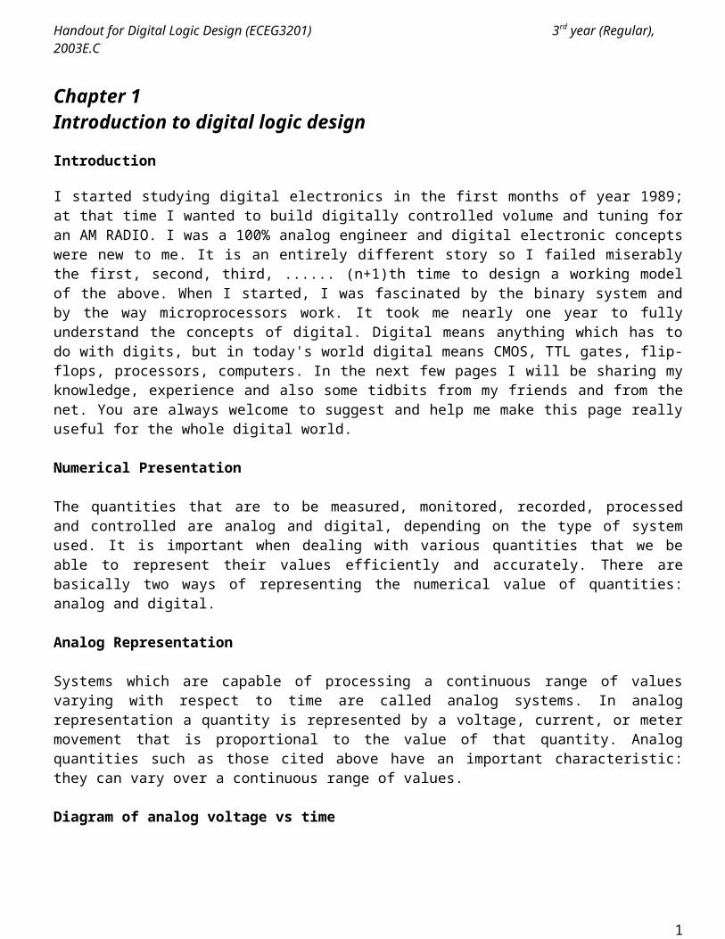
Systems which are capable of processing a continuous range of values varying with respect to time are called analog systems. In analog representation a quantity is represented by a voltage, current, or meter movement that is proportional to the value of that quantity. Analog quantities such as those cited above have an important characteristic: they can vary over a continuous range of values.
Diagram of analog voltage vs time
Digital Representation
Systems which process discrete values are called digital systems. In digital representation the quantities are represented not by proportional quantities but by symbols called digits. As an example, consider the digital watch, which provides the time of the day in the form of decimal digits representing hours and minutes (and sometimes seconds). As we know, time of day changes continuously, but the digital watch reading does not
1
Handout for Digital Logic Design (ECEG3201) 3rd year (Regular), 2003E.C
change continuously; rather, it changes in steps of one per minute (or per second). In other words, time of day digital representation changes in discrete steps, as compared to the representation of time provided by an analog watch, where the dial reading changes continuously.
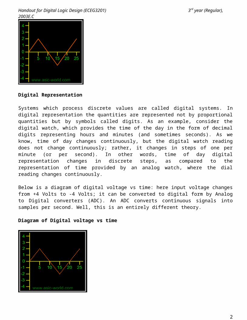
Below is a diagram of digital voltage vs time: here input voltage changes from +4 Volts to -4 Volts; it can be converted to digital form by Analog to Digital converters (ADC). An ADC converts continuous signals into samples per second. Well, this is an entirely different theory.
Diagram of Digital voltage vs time
The major difference between analog and digital quantities, then, can be stated simply as follows: Analog = continuous Digital = discrete (step by step)
Advantages of Digital Techniques
Easier to design. Exact values of voltage or current are not important, only the range (HIGH or LOW) in which they fall.
Information storage is easy. Accuracy and precision are greater. Operations can be programmed. Analog systems can also be programmed, but the available operations
variety and complexity is severely limited. Digital circuits are less affected by noise, as long as the noise is not large enough to prevent us from
distinguishing HIGH from LOW (we discuss this in detail in an advanced digital tutorial section). More digital circuitry can be fabricated on IC chips.
Limitations of Digital Techniques
Most physical quantities in real world are analog in nature, and these quantities are often the inputs and outputs that are being monitored, operated on, and controlled by a system. Thus conversion to digital format and re-conversion to analog format is needed.
Numbering System
Many number systems are in use in digital technology. The most common are the decimal, binary, octal, and hexadecimal systems. The decimal system is clearly the most familiar to us because it is a tool that we use every day. Examining some of its characteristics will help us to better understand the other systems. In the next few pages we shall introduce four numerical representation systems that are used in the digital system. There are other systems, which we will look at briefly.
2
Handout for Digital Logic Design (ECEG3201) 3rd year (Regular), 2003E.C
Decimal Binary Octal Hexadecimal
Decimal System
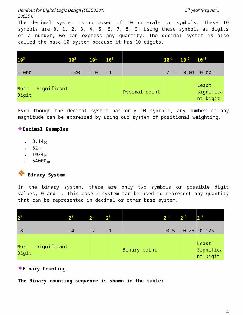
The decimal system is composed of 10 numerals or symbols. These 10 symbols are 0, 1, 2, 3, 4, 5, 6, 7, 8, 9. Using these symbols as digits of a number, we can express any quantity. The decimal system is also called the base-10 system because it has 10 digits.
103 102 101 100 10-1 10-2 10-3
=1000 =100 =10 =1 . =0.1 =0.01 =0.001
Most Significant Digit Decimal pointLeast Significant Digit
Even though the decimal system has only 10 symbols, any number of any magnitude can be expressed by using our system of positional weighting.
Decimal Examples
3.1410
5210
102410 6400010
Binary System
In the binary system, there are only two symbols or possible digit values, 0 and 1. This base-2 system can be used to represent any quantity that can be represented in decimal or other base system.
23 22 21 20 2-1 2-2 2-3
=8 =4 =2 =1 . =0.5 =0.25 =0.125
Most Significant Digit Binary pointLeast Significant Digit
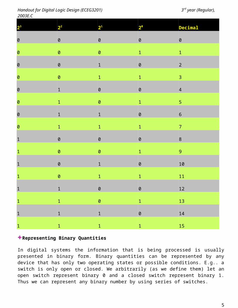
Binary Counting
The Binary counting sequence is shown in the table:
23 22 21 20 Decimal
3
Handout for Digital Logic Design (ECEG3201) 3rd year (Regular), 2003E.C
0 0 0 0 0
0 0 0 1 1
0 0 1 0 2
0 0 1 1 3
0 1 0 0 4
0 1 0 1 5
0 1 1 0 6
0 1 1 1 7
1 0 0 0 8
1 0 0 1 9
1 0 1 0 10
1 0 1 1 11
1 1 0 0 12
1 1 0 1 13
1 1 1 0 14
1 1 1 1 15
Representing Binary Quantities
In digital systems the information that is being processed is usually presented in binary form. Binary quantities can be represented by any device that has only two operating states or possible conditions. E.g.. a switch is only open or closed. We arbitrarily (as we define them) let an open switch represent binary 0 and a closed switch represent binary 1. Thus we can represent any binary number by using series of switches.
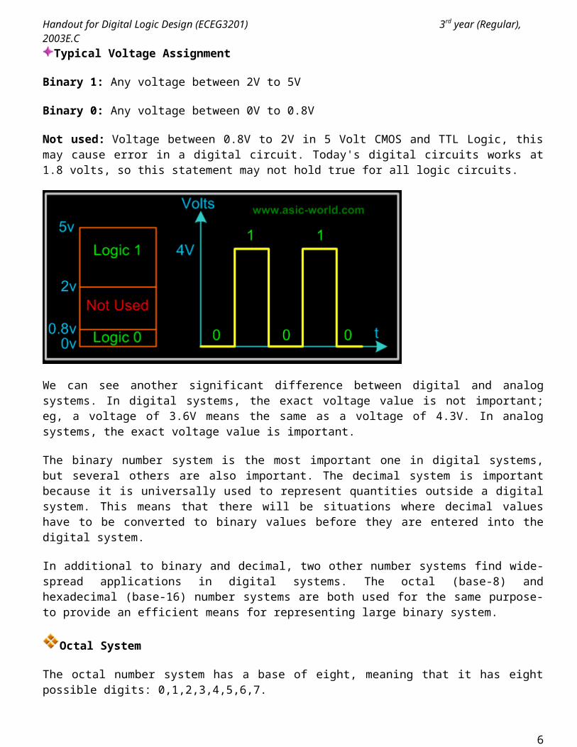
Typical Voltage Assignment
Binary 1: Any voltage between 2V to 5V
Binary 0: Any voltage between 0V to 0.8V
Not used: Voltage between 0.8V to 2V in 5 Volt CMOS and TTL Logic, this may cause error in a digital circuit. Today's digital circuits works at 1.8 volts, so this statement may not hold true for all logic circuits.
4
Handout for Digital Logic Design (ECEG3201) 3rd year (Regular), 2003E.C
We can see another significant difference between digital and analog systems. In digital systems, the exact voltage value is not important; eg, a voltage of 3.6V means the same as a voltage of 4.3V. In analog systems, the exact voltage value is important.
The binary number system is the most important one in digital systems, but several others are also important. The decimal system is important because it is universally used to represent quantities outside a digital system. This means that there will be situations where decimal values have to be converted to binary values before they are entered into the digital system.
In additional to binary and decimal, two other number systems find wide-spread applications in digital systems. The octal (base-8) and hexadecimal (base-16) number systems are both used for the same purpose- to provide an efficient means for representing large binary system.
Octal System
The octal number system has a base of eight, meaning that it has eight possible digits: 0,1,2,3,4,5,6,7.
83 82 81 80 8-1 8-2 8-3
=512 =64 =8 =1 . =1/8 =1/64 =1/512
Most Significant Digit Octal pointLeast Significant Digit
Octal to Decimal Conversion
2378 = 2 x (82) + 3 x (81) + 7 x (80) = 15910
24.68 = 2 x (81) + 4 x (80) + 6 x (8-1) = 20.7510
11.18 = 1 x (81) + 1 x (80) + 1 x (8-1) = 9.12510
12.38 = 1 x (81) + 2 x (80) + 3 x (8-1) = 10.37510
Hexadecimal System
5
Handout for Digital Logic Design (ECEG3201) 3rd year (Regular), 2003E.C
The hexadecimal system uses base 16. Thus, it has 16 possible digit symbols. It uses the digits 0 through 9 plus the letters A, B, C, D, E, and F as the 16 digit symbols.
163 162 161 160 16-1 16-2 16-3
=4096 =256 =16 =1 . =1/16 =1/256 =1/4096
Most Significant Digit Hexa Decimal pointLeast Significant Digit
Hexadecimal to Decimal Conversion
24.616 = 2 x (161) + 4 x (160) + 6 x (16-1) = 36.37510
11.116 = 1 x (161) + 1 x (160) + 1 x (16-1) = 17.062510
12.316 = 1 x (161) + 2 x (160) + 3 x (16-1) = 18.187510
Code Conversion
Converting from one code form to another code form is called code conversion, like converting from binary to decimal or converting from hexadecimal to decimal.
Binary-To-Decimal Conversion
Any binary number can be converted to its decimal equivalent simply by summing together the weights of the various positions in the binary number which contain a 1.
Binary Decimal
110112
24+23+01+21+20 =16+8+0+2+1
Result 2710
And
Binary Decimal
101101012
27+06+25+24+03+22+01+20 =128+0+32+16+0+4+0+1
Result 18110
You should have noticed that the method is to find the weights (i.e., powers of 2) for each bit position that contains a 1, and then to add them up.
6
Handout for Digital Logic Design (ECEG3201) 3rd year (Regular), 2003E.C
Decimal-To-Binary Conversion
There are 2 methods:
Reverse of Binary-To-Decimal Method Repeat Division
Reverse of Binary-To-Decimal Method
Decimal Binary
4510 =32 + 0 + 8 + 4 +0 + 1
=25+0+23+22+0+20
Result =1011012
Repeat Division-Convert decimal to binary
This method uses repeated division by 2.
Convert 2510 to binary
Division Remainder Binary
25/2 = 12+ remainder of 1 1 (Least Significant Bit)
12/2 = 6 + remainder of 0 0
6/2 = 3 + remainder of 0 0
3/2 = 1 + remainder of 1 1
1/2 = 0 + remainder of 1 1 (Most Significant Bit)
Result 2510 = 110012
The Flow chart for repeated-division method is as follows:
7
Handout for Digital Logic Design (ECEG3201) 3rd year (Regular), 2003E.C
Binary-To-Octal / Octal-To-Binary Conversion
Octal Digit 0 1 2 3 4 5 6 7
Binary Equivalent 000 001 010 011 100 101 110 111
Each Octal digit is represented by three binary digits.
Example:
100 111 0102 = (100) (111) (010)2 = 4 7 28
Repeat Division-Convert decimal to octal
This method uses repeated division by 8.
Example: Convert 17710 to octal and binary
Division Result Binary
177/8 = 22+ remainder of 1 1 (Least Significant Bit)
22/ 8 = 2 + remainder of 6 6
2 / 8 = 0 + remainder of 2 2 (Most Significant Bit)
Result 17710 = 2618
Binary = 0101100012
8
Handout for Digital Logic Design (ECEG3201) 3rd year (Regular), 2003E.C
Hexadecimal to Decimal/Decimal to Hexadecimal Conversion
Example:
2AF16 = 2 x (162) + 10 x (161) + 15 x (160) = 68710
Repeat Division- Convert decimal to hexadecimal
This method uses repeated division by 16.
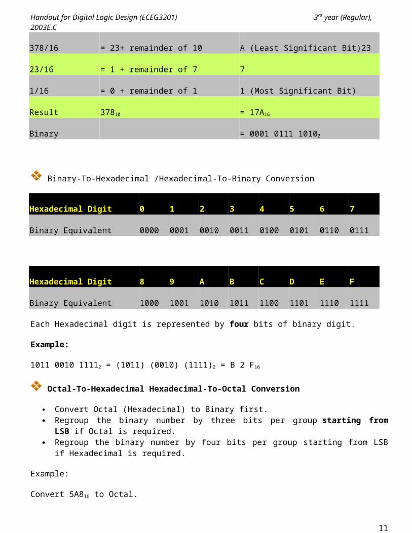
Example: convert 37810 to hexadecimal and binary:
Division Result Hexadecimal
378/16 = 23+ remainder of 10 A (Least Significant Bit)23
23/16 = 1 + remainder of 7 7
1/16 = 0 + remainder of 1 1 (Most Significant Bit)
Result 37810 = 17A16
Binary = 0001 0111 10102
Binary-To-Hexadecimal /Hexadecimal-To-Binary Conversion
Hexadecimal Digit 0 1 2 3 4 5 6 7
Binary Equivalent 0000 0001 0010 0011 0100 0101 0110 0111
Hexadecimal Digit 8 9 A B C D E F
Binary Equivalent 1000 1001 1010 1011 1100 1101 1110 1111
Each Hexadecimal digit is represented by four bits of binary digit.
Example:
1011 0010 11112 = (1011) (0010) (1111)2 = B 2 F16
Octal-To-Hexadecimal Hexadecimal-To-Octal Conversion
9
Handout for Digital Logic Design (ECEG3201) 3rd year (Regular), 2003E.C
Convert Octal (Hexadecimal) to Binary first. Regroup the binary number by three bits per group starting from LSB if Octal is required. Regroup the binary number by four bits per group starting from LSB if Hexadecimal is required.
Example:
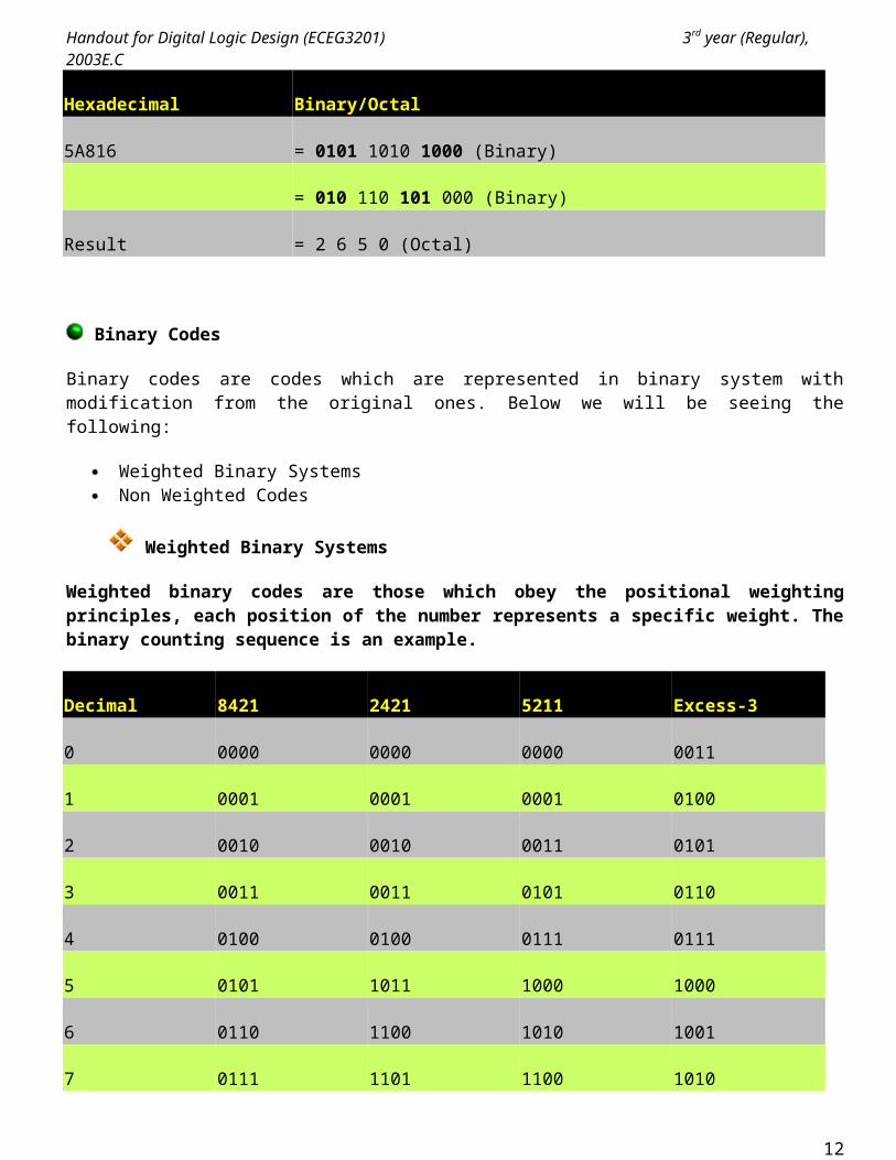
Convert 5A816 to Octal.
Hexadecimal Binary/Octal
5A816 = 0101 1010 1000 (Binary)
= 010 110 101 000 (Binary)
Result = 2 6 5 0 (Octal)
Binary Codes
Binary codes are codes which are represented in binary system with modification from the original ones. Below we will be seeing the following:
Weighted Binary Systems Non Weighted Codes
Weighted Binary Systems
Weighted binary codes are those which obey the positional weighting principles, each position of the number represents a specific weight. The binary counting sequence is an example.
Decimal 8421 2421 5211 Excess-3
0 0000 0000 0000 0011
1 0001 0001 0001 0100
2 0010 0010 0011 0101
3 0011 0011 0101 0110
4 0100 0100 0111 0111
5 0101 1011 1000 1000
6 0110 1100 1010 1001
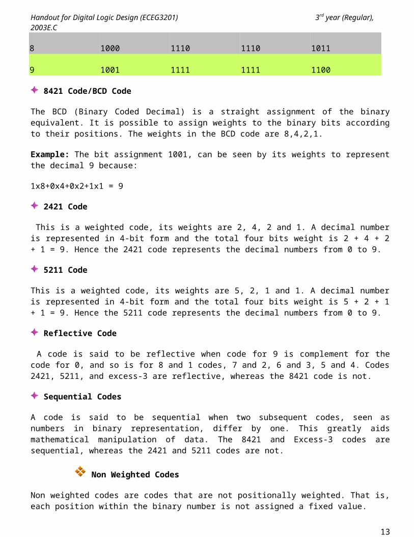
10
Handout for Digital Logic Design (ECEG3201) 3rd year (Regular), 2003E.C
7 0111 1101 1100 1010
8 1000 1110 1110 1011
9 1001 1111 1111 1100
8421 Code/BCD Code
The BCD (Binary Coded Decimal) is a straight assignment of the binary equivalent. It is possible to assign weights to the binary bits according to their positions. The weights in the BCD code are 8,4,2,1.
Example: The bit assignment 1001, can be seen by its weights to represent the decimal 9 because:
1x8+0x4+0x2+1x1 = 9
2421 Code
This is a weighted code, its weights are 2, 4, 2 and 1. A decimal number is represented in 4-bit form and the total four bits weight is 2 + 4 + 2 + 1 = 9. Hence the 2421 code represents the decimal numbers from 0 to 9.
5211 Code
This is a weighted code, its weights are 5, 2, 1 and 1. A decimal number is represented in 4-bit form and the total four bits weight is 5 + 2 + 1 + 1 = 9. Hence the 5211 code represents the decimal numbers from 0 to 9.
Reflective Code
A code is said to be reflective when code for 9 is complement for the code for 0, and so is for 8 and 1 codes, 7 and 2, 6 and 3, 5 and 4. Codes 2421, 5211, and excess-3 are reflective, whereas the 8421 code is not.
Sequential Codes
A code is said to be sequential when two subsequent codes, seen as numbers in binary representation, differ by one. This greatly aids mathematical manipulation of data. The 8421 and Excess-3 codes are sequential, whereas the 2421 and 5211 codes are not.
Non Weighted Codes
Non weighted codes are codes that are not positionally weighted. That is, each position within the binary number is not assigned a fixed value.
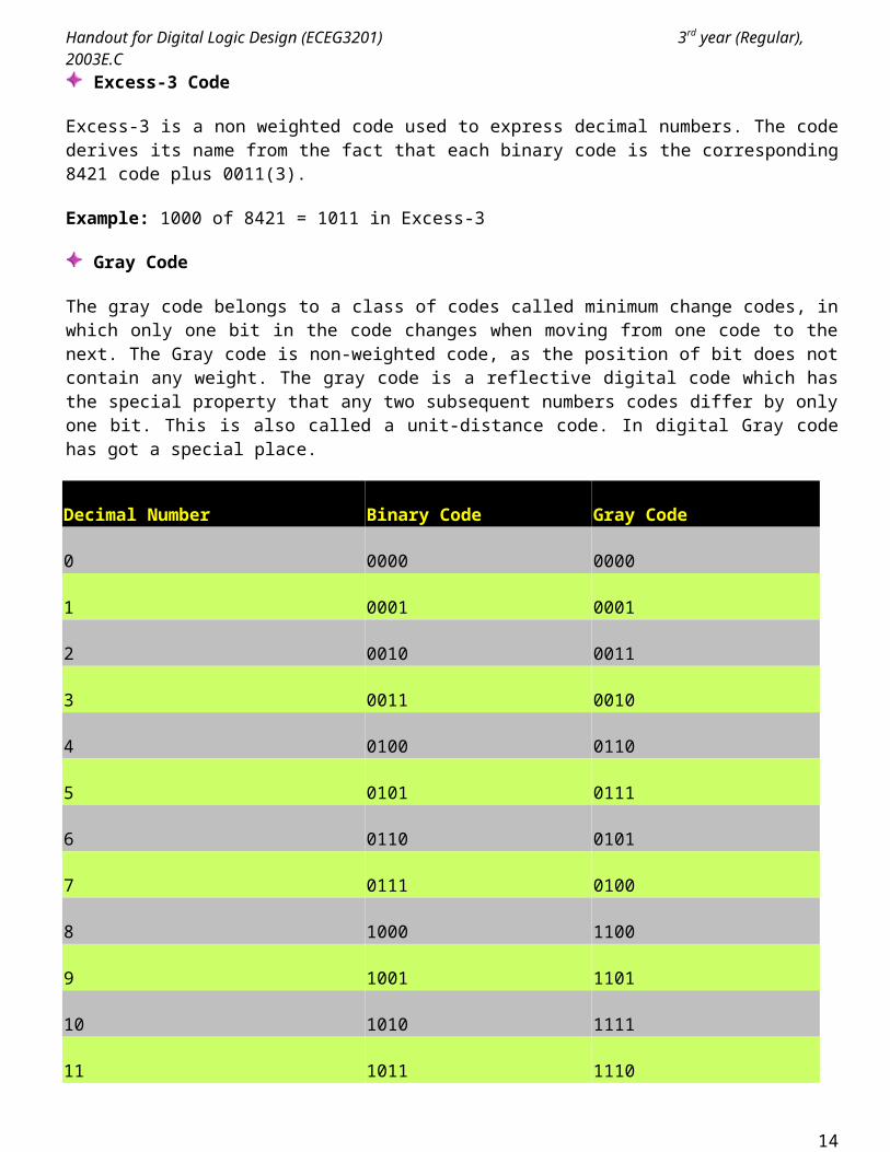
Excess-3 Code
Excess-3 is a non weighted code used to express decimal numbers. The code derives its name from the fact that each binary code is the corresponding 8421 code plus 0011(3).
Example: 1000 of 8421 = 1011 in Excess-3
Gray Code
11
Handout for Digital Logic Design (ECEG3201) 3rd year (Regular), 2003E.C
The gray code belongs to a class of codes called minimum change codes, in which only one bit in the code changes when moving from one code to the next. The Gray code is non-weighted code, as the position of bit does not contain any weight. The gray code is a reflective digital code which has the special property that any two subsequent numbers codes differ by only one bit. This is also called a unit-distance code. In digital Gray code has got a special place.
Decimal Number Binary Code Gray Code
0 0000 0000
1 0001 0001
2 0010 0011
3 0011 0010
4 0100 0110
5 0101 0111
6 0110 0101
7 0111 0100
8 1000 1100
9 1001 1101
10 1010 1111
11 1011 1110
12 1100 1010
13 1101 1011
14 1110 1001
15 1111 1000
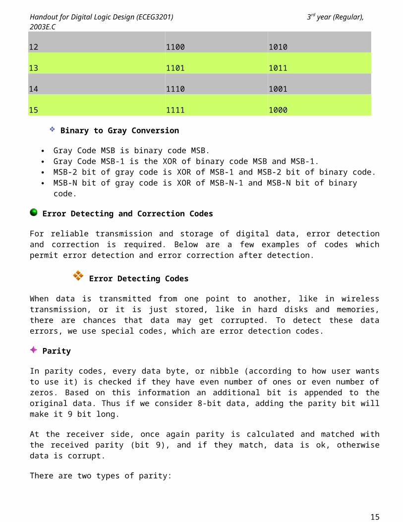
Binary to Gray Conversion
Gray Code MSB is binary code MSB. Gray Code MSB-1 is the XOR of binary code MSB and MSB-1. MSB-2 bit of gray code is XOR of MSB-1 and MSB-2 bit of binary code. MSB-N bit of gray code is XOR of MSB-N-1 and MSB-N bit of binary code.
Error Detecting and Correction Codes
12
Handout for Digital Logic Design (ECEG3201) 3rd year (Regular), 2003E.C
For reliable transmission and storage of digital data, error detection and correction is required. Below are a few examples of codes which permit error detection and error correction after detection.
Error Detecting Codes
When data is transmitted from one point to another, like in wireless transmission, or it is just stored, like in hard disks and memories, there are chances that data may get corrupted. To detect these data errors, we use special codes, which are error detection codes.
Parity
In parity codes, every data byte, or nibble (according to how user wants to use it) is checked if they have even number of ones or even number of zeros. Based on this information an additional bit is appended to the original data. Thus if we consider 8-bit data, adding the parity bit will make it 9 bit long.
At the receiver side, once again parity is calculated and matched with the received parity (bit 9), and if they match, data is ok, otherwise data is corrupt.
There are two types of parity:
Even parity: Checks if there is an even number of ones; if so, parity bit is zero. When the number of ones is odd then parity bit is set to 1.
Odd Parity: Checks if there is an odd number of ones; if so, parity bit is zero. When number of ones is even then parity bit is set to 1
Check Sums
The parity method is calculated over byte, word or double word. But when errors need to be checked over 128 bytes or more (basically blocks of data), then calculating parity is not the right way. So we have checksum, which allows to check for errors on block of data. There are many variations of checksum.
Adding all bytes CRC Fletcher's checksum Adler-32
The simplest form of checksum, which simply adds up the asserted bits in the data, cannot detect a number of types of errors. In particular, such a checksum is not changed by:
Reordering of the bytes in the message Inserting or deleting zero-valued bytes Multiple errors which sum to zero
Example of Checksum : Given 4 bytes of data (can be done with any number of bytes): 25h, 62h, 3Fh, 52h
Adding all bytes together gives 118h. Drop the Carry Nibble to give you 18h. Get the two's complement of the 18h to get E8h. This is the checksum byte.
To Test the Checksum byte simply add it to the original group of bytes. This should give you 200h.
13
Handout for Digital Logic Design (ECEG3201) 3rd year (Regular), 2003E.C
Drop the carry nibble again giving 00h. Since it is 00h this means the checksum means the bytes were probably not changed.
Error-Correcting Codes
Error-correcting codes not only detect errors, but also correct them. This is used normally in Satellite communication, where turn-around delay is very high as is the probability of data getting corrupt.
ECC (Error correcting codes) are used also in memories, networking, Hard disk, CDROM, DVD etc. Normally in networking chips (ASIC), we have 2 Error detection bits and 1 Error correction bit.
Hamming Code
Hamming code adds a minimum number of bits to the data transmitted in a noisy channel, to be able to correct every possible one-bit error. It can detect (not correct) two-bits errors and cannot distinguish between 1-bit and 2-bits inconsistencies. It can't - in general - detect 3(or more)-bits errors.
The idea is that the failed bit position in an n-bit string (which we'll call X) can be represented in binary with log2(n) bits, hence we'll try to get it adding just log2(n) bits.
First, we set m = n + log2(n) to the encoded string length and we number each bit position starting from 1 through m. Then we place these additional bits at power-of-two positions, that is 1, 2, 4, 8..., while remaining ones (3, 5, 6, 7...) hold the bit string in the original order.
Now we set each added bit to the parity of a group of bits. We group bits this way: we form a group for every parity bit, where the following relation holds:
position(bit) AND position(parity) = position(parity)
(Note that: AND is the bit-wise boolean AND; parity bits are included in the groups; each bit can belong to one or more groups.)
So bit 1 groups bits 1, 3, 5, 7... while bit 2 groups bits 2, 3, 6, 7, 10... , bit 4 groups bits 4, 5, 6, 7, 12, 13... and so on.
Thus, by definition, X (the failed bit position defined above) is the sum of the incorrect parity bits positions (0 for no errors).
To understand why it is so, let's call Xn the nth bit of X in binary representation. Now consider that each parity bit is tied to a bit of X: parity1 -> X1, parity2 -> X2, parity4 -> X3, parity8 -> X4 and so on - for programmers: they are the respective AND masks -. By construction, the failed bit makes fail only the parity bits which correspond to the 1s in X, so each bit of X is 1 if the corresponding parity is wrong and 0 if it is correct.
Note that the longer the string, the higher the throughput n/m and the lower the probability that no more than one bit fails. So the string to be sent should be broken into blocks whose length depends on the transmission channel quality (the cleaner the channel, the bigger the block). Also, unless it's guaranteed that at most one bit per block fails, a checksum or some other form of data integrity check should be added.
Alphanumeric Codes
14
Handout for Digital Logic Design (ECEG3201) 3rd year (Regular), 2003E.C
The binary codes that can be used to represent all the letters of the alphabet, numbers and mathematical symbols, punctuation marks, are known as alphanumeric codes or character codes. These codes enable us to interface the input-output devices like the keyboard, printers, video displays with the computer.
ASCII Code
ASCII stands for American Standard Code for Information Interchange. It has become a world standard alphanumeric code for microcomputers and computers. It is a 7-bit code representing 2 7 = 128 different characters. These characters represent 26 upper case letters (A to Z), 26 lowercase letters (a to z), 10 numbers (0 to 9), 33 special characters and symbols and 33 control characters.
The 7-bit code is divided into two portions, The leftmost 3 bits portion is called zone bits and the 4-bit portion on the right is called numeric bits.
An 8-bit version of ASCII code is known as USACC-II 8 or ASCII-8. The 8-bit version can represent a maximum of 256 characters.
EBCDIC Code
EBCDIC stands for Extended Binary Coded Decimal Interchange. It is mainly used with large computer systems like mainframes. EBCDIC is an 8-bit code and thus accomodates up to 256 characters. An EBCDIC code is divided into two portions: 4 zone bits (on the left) and 4 numeric bits (on the right).
Floating Point Numbers
A real number or floating point number is a number which has both an integer and a fractional part. Examples for real real decimal numbers are 123.45, 0.1234, -0.12345, etc. Examples for real binary numbers are 1100.1100, 0.1001, -1.001, etc. In general, floating point numbers are expressed in exponential notation.
For example the decimal number
30000.0 can be written as 3 x 10⁴. 312.45 can be written as 3.1245 x 10².
Similarly, the binary number 1010.001 can be written as 1.010001 x 10³.
The general form of a number N can be expressed as
N = ± m x b±e.
Where m is mantissa, b is the base of number system and e is the exponent. A floating point number is represented by two parts. The number first part, called mantissa, is a signed fixed point number and the second part, called exponent, specifies the decimal or binary position.
Binary Representation of Floating Point Numbers
A floating point binary number is also represented as in the case of decimal numbers. It means that mantissa and exponent are expressed using signed magnitude notation in which one bit is reserved for sign bit.
15
Handout for Digital Logic Design (ECEG3201) 3rd year (Regular), 2003E.C
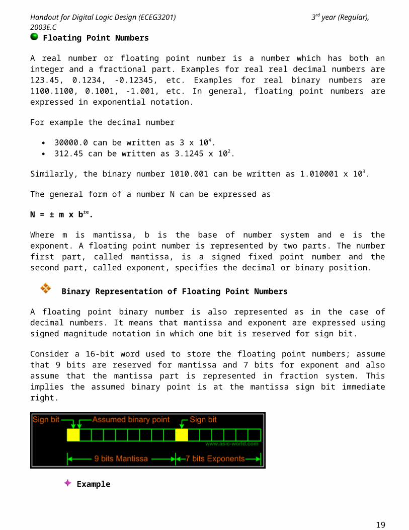
Consider a 16-bit word used to store the floating point numbers; assume that 9 bits are reserved for mantissa and 7 bits for exponent and also assume that the mantissa part is represented in fraction system. This implies the assumed binary point is at the mantissa sign bit immediate right.
Example
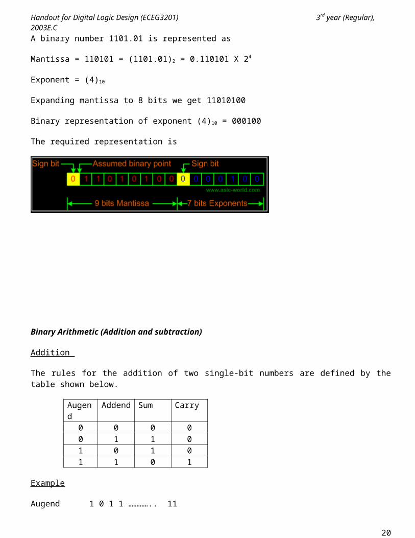
A binary number 1101.01 is represented as
Mantissa = 110101 = (1101.01)2 = 0.110101 X 24
Exponent = (4)10
Expanding mantissa to 8 bits we get 11010100
Binary representation of exponent (4)10 = 000100
The required representation is
Binary Arithmetic (Addition and subtraction)
Addition
The rules for the addition of two single-bit numbers are defined by the table shown below.
Augend Addend Sum Carry0 0 0 00 1 1 0
16
Handout for Digital Logic Design (ECEG3201) 3rd year (Regular), 2003E.C
1 0 1 01 1 0 1
Example
Augend 1 0 1 1 ………….. 11
Addend 0 1 1 1 ………….. +7
___________________
Sum 1 0 0 1 0 (n+1) bits generated
Carry 1 1 1 1 the carry ripples/ moves
o When two n-bit numbers, whose most significant digits are 1, are added together they will generate an (n+1)-bit sum. The additional bit generated is termed arithmetic overflow.
Subtraction
Rules for the subtraction of two binary digits
Minued Subtrahend Difference Borrow0 0 0 00 1 1 01 0 1 01 1 0 1
Example1
Minued 1 1 0 0 12
Subtrahend 0 0 1 1 -3
Difference 1 0 0 1 9
Borrows 1 1
Example 2
If the subtrahend is greater than the minued arithmetic underflow occurs which results in a borrow-out at the MSB & the difference is negative
Minued 0 0 1 1 3
Subtrahend 1 1 0 0 -12
Difference 0 1 1 1 -9
Borrows 1 1
ComplementsComplements are used in digital computers for simplifying the subtraction operation and for logical manipulation. There are two types of complements for each base-r systems: the radix complement and the diminished radix complement. The first is referred to as the r’s complement and the second as the (r-1)’s complement. When the value of the base r is substituted in the name, the two types are referred to as the 2’s complement and 1’s complement for the binary numbers, and the 10’s complement and 9’s complement for the decimal numbers.
17
Handout for Digital Logic Design (ECEG3201) 3rd year (Regular), 2003E.C
Diminished Radix complementGiven a number N in base r having n digits, the (r-1)’s complement of N is defined as (rn - 1) – N. For decimal numbers, r = 10 and r-1= 9, so the 9’s complement of N is (10n -1) – N. Now, 10n represents a number that consists of a single 1 followed by n 0’s. 10n -1 is a number represented by n 9’s. For example, if n=4, we have 104 = 10,000 and 104 – 1 = 9999. It follows that the 9’s complement of a decimal number is obtained by subtracting each digit from 9.some numerical examples follow. The 9’s complement of 5467000 is 999999 – 546700 = 453299 The 9’s complement of 012398 is 999999 – 012398 = 987601For binary numbers, r=2 and r-1=1, so the 1’s complement of N is (2n -1) –N. again, 2n is represented by a binary number that consists of a 1 followed by n 0’s. 2n -1 is a binary number represented by n 1’s. For example, if n=4, we have 24 = (10000)2 and 24 -1 = (1111)2. Thus the 1’s complement of a binary number is obtained by subtracting each digit from 1. However, when subtracting binary digits from 1, we can have either 1-0 = 1 or 1-1= 0, which causes the bit to change from 0 to 1 or from 1 to 0. Therefore, the 1’s complement of a binary number is formed by changing 1’s to 0’s and 0’s to 1’s. The following are some numerical examples. The 1’s complement of 1011000 is 0100111. The 1’s complement of 0101101 is 1010010The (r-1)’s complement of octal or hexadecimal number is obtained by subtracting each digit from 7 or F (decimal 15), respectively.
Radix ComplementThe r’s complement of an n-bit number N in base r is defined as r n –n for N0 and 0 for N=0. Comparing with the (r-1)’s complement, we note that the r’s complement is obtained by adding 1 to the (r-1)’s complement since rn –N = [(rn -1) –N + 1]. Thus, the 10’s complement of decimal 2389 is 7610 + 1 = 7611 and is obtained by adding 1 to the 9’s complement value. The 2’s complement of binary 101100 is 010011 + 1 = 010100 and is obtained by adding 1 to the 1’s complement value.
Since 10n is a number represented by a 1 followed by n 0’s, 10n –N, which is the 10’s complement of N, can be formed also by leaving all least significant 0’s unchanged, subtracting the first nonzero least significant digit from 10, and subtracting all higher significant digits from 9. The 10’s complement of 012398 is 987602 The 10’s complement of 246700 is 753300The 10’s complement of the first number is obtained by subtracting 8 from 10 in the least significant position and subtracting all other digits from 9. The 10’s complement of the second number is obtained by leaving the two least significant 0’s unchanged, subtracting 7 from 10, and subtracting the other three digits from 9.Similarly, the 2’s complement can be formed by leaving all least significant 0’s and the first 1 unchanged, and replacing 1’s with 0’s and 0’s with 1’s in all other higher significant digits. The 2’s complement of 1101100 is 0010100. The 2’s complement of 0110111 is 1001001.The 2’s complement of the first number is obtained by leaving the two least significant 0’s and the first 1 unchanged, and then replacing 1’s with 0;s and 0;s with 1’s in the other four most significant digits. The 2’s complement of the second number is obtained by leaving the least significant 1 unchanged and complementing all other digits.
In the previous definitions, it was assumed that the numbers do not have a radix point. If the original number N contains a radix point, the point should be removed temporarily in order to form the r’s or (r-1)’s complement. The radix point is then restored to the complemented number in the same relative position. It is also worth mentioning that the complement of the complement restores the number to its original value. The
18
Handout for Digital Logic Design (ECEG3201) 3rd year (Regular), 2003E.C
r’s complement of N is rn –N. the complement of the complement is rn –(rn –N) = N, giving back the original number.
Chapter 2 Basic and derived logic gates, logic families
Symbolic Logic
Boolean algebra derives its name from the mathematician George Boole. Symbolic Logic uses values, variables and operations:
19
Handout for Digital Logic Design (ECEG3201) 3rd year (Regular), 2003E.C
True is represented by the value 1. False is represented by the value 0.
Variables are represented by letters and can have one of two values, either 0 or 1. Operations are functions of one or more variables.
AND is represented by X.Y OR is represented by X + Y NOT is represented by X'. Throughout this tutorial the X' form will be used and sometime! X will be
used.
These basic operations can be combined to give expressions.
Example:
X X.Y W.X.Y + Z
Precedence
As with any other branch of mathematics, these operators have an order of precedence. NOT operations have the highest precedence, followed by AND operations, followed by OR operations. Brackets can be used as with other forms of algebra. e.g.
X.Y + Z and X.(Y + Z) are not the same function.
Function Definitions
The logic operations given previously are defined as follows:
Define f(X,Y) to be some function of the variables X and Y.
f(X,Y) = X.Y
1 if X = 1 and Y = 1 0 Otherwise
f(X,Y) = X + Y
1 if X = 1 or Y = 1 0 Otherwise
f(X) = X' 1 if X = 0 0 Otherwise
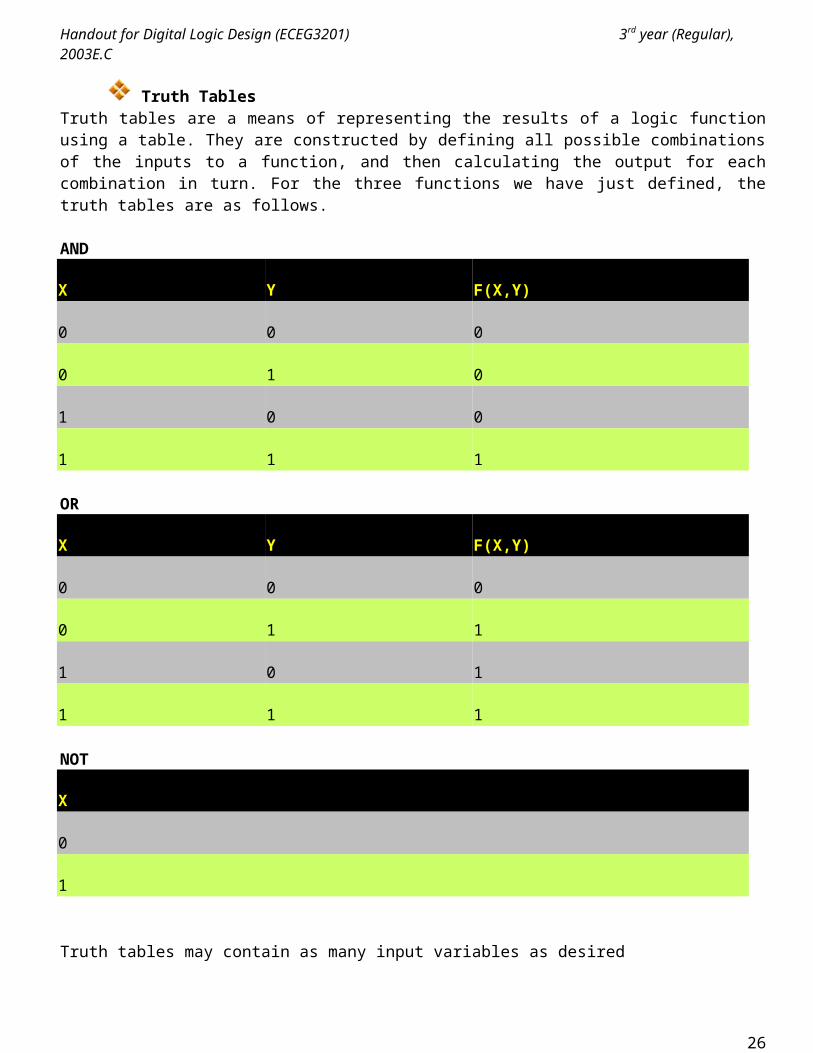
Truth Tables
20
Handout for Digital Logic Design (ECEG3201) 3rd year (Regular), 2003E.C
Truth tables are a means of representing the results of a logic function using a table. They are constructed by defining all possible combinations of the inputs to a function, and then calculating the output for each combination in turn. For the three functions we have just defined, the truth tables are as follows.
AND
X Y F(X,Y)
0 0 0
0 1 0
1 0 0
1 1 1
OR
X Y F(X,Y)
0 0 0
0 1 1
1 0 1
1 1 1
NOT
X
0
1
Truth tables may contain as many input variables as desired
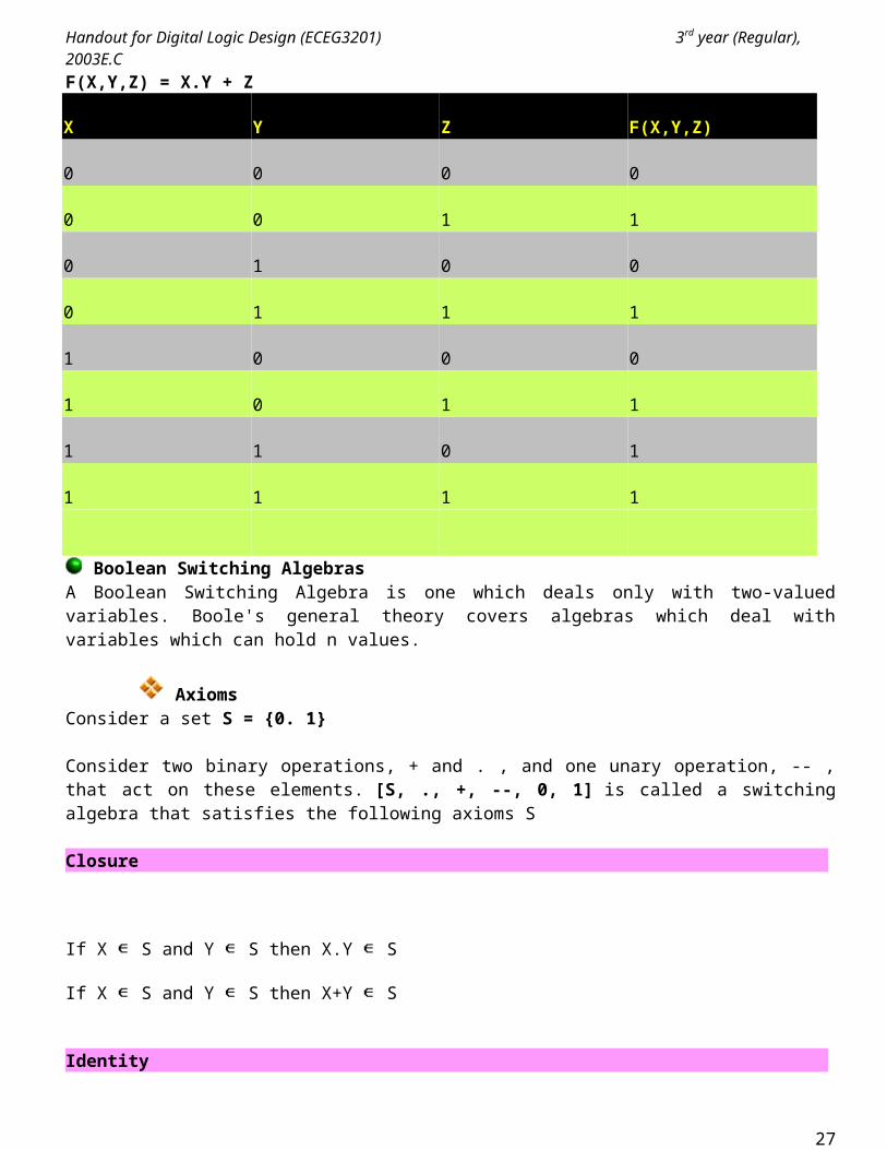
F(X,Y,Z) = X.Y + Z
X Y Z F(X,Y,Z)
0 0 0 0
0 0 1 1
0 1 0 0
21
Handout for Digital Logic Design (ECEG3201) 3rd year (Regular), 2003E.C
0 1 1 1
1 0 0 0
1 0 1 1
1 1 0 1
1 1 1 1
Boolean Switching AlgebrasA Boolean Switching Algebra is one which deals only with two-valued variables. Boole's general theory covers algebras which deal with variables which can hold n values.
AxiomsConsider a set S = {0. 1}
Consider two binary operations, + and . , and one unary operation, -- , that act on these elements. [S, ., +, --, 0, 1] is called a switching algebra that satisfies the following axioms S
Closure
If X S and Y S then X.Y S
If X S and Y S then X+Y S
Identity
an identity 0 for + such that X + 0 = X
an identity 1 for . such that X . 1 = X
Commutative Laws
X + Y = Y + X
X . Y = Y . X
Distributive Laws
22
Handout for Digital Logic Design (ECEG3201) 3rd year (Regular), 2003E.C
X.(Y + Z ) = X.Y + X.Z
X + Y.Z = (X + Y) . (X + Z)
Complement
X S a complement X' such that
X + X' = 1
X . X' = 0
The complement X' is unique.
TheoremsA number of theorems may be proved for switching algebras
Idempotent Law
X + X = X
X . X = X
DeMorgan's Law
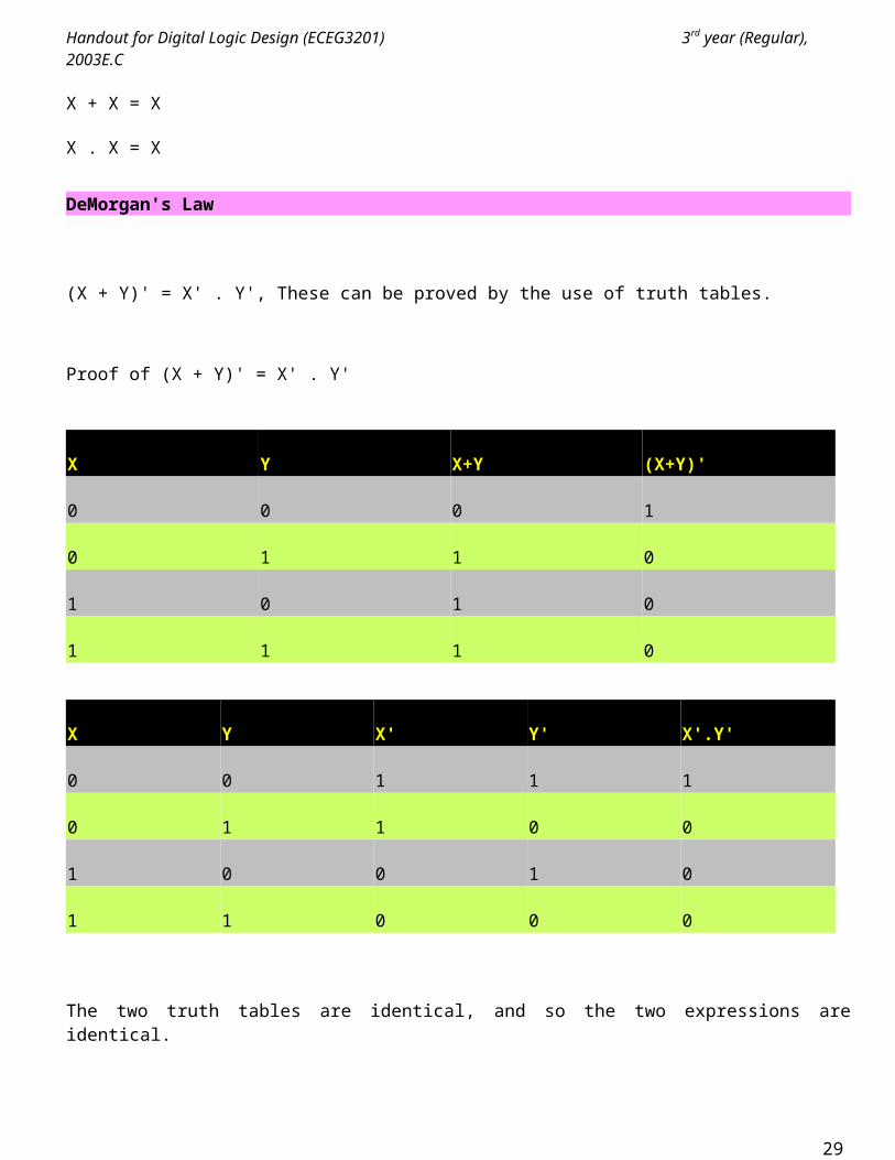
(X + Y)' = X' . Y', These can be proved by the use of truth tables.
Proof of (X + Y)' = X' . Y'
X Y X+Y (X+Y)'
0 0 0 1
0 1 1 0
1 0 1 0
23
Handout for Digital Logic Design (ECEG3201) 3rd year (Regular), 2003E.C
1 1 1 0
X Y X' Y' X'.Y'
0 0 1 1 1
0 1 1 0 0
1 0 0 1 0
1 1 0 0 0
The two truth tables are identical, and so the two expressions are identical.
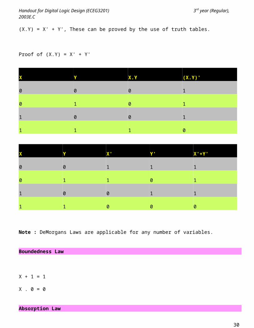
(X.Y) = X' + Y', These can be proved by the use of truth tables.
Proof of (X.Y) = X' + Y'
X Y X.Y (X.Y)'
0 0 0 1
0 1 0 1
1 0 0 1
1 1 1 0
X Y X' Y' X'+Y'
0 0 1 1 1
0 1 1 0 1
1 0 0 1 1
1 1 0 0 0
24
Handout for Digital Logic Design (ECEG3201) 3rd year (Regular), 2003E.C
Note : DeMorgans Laws are applicable for any number of variables.
Boundedness Law
X + 1 = 1
X . 0 = 0
Absorption Law
X + (X . Y) = X
X . (X + Y ) = X
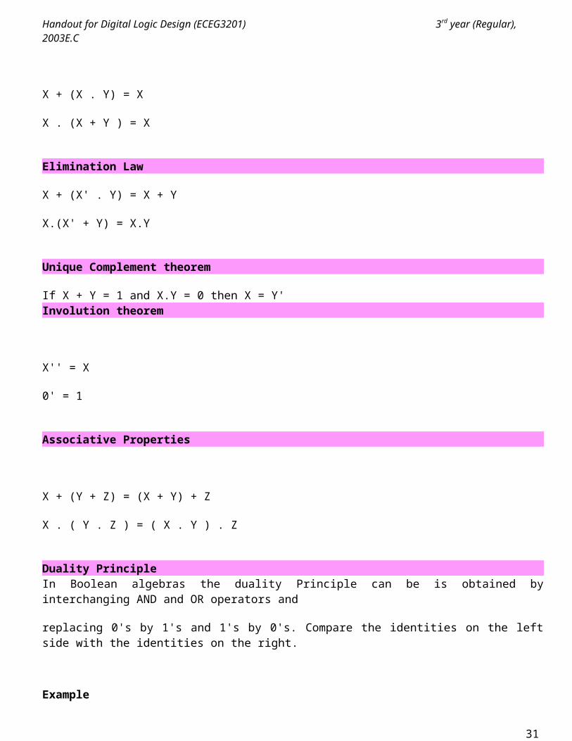
Elimination Law
X + (X' . Y) = X + Y
X.(X' + Y) = X.Y
Unique Complement theorem
If X + Y = 1 and X.Y = 0 then X = Y'Involution theorem
X'' = X
0' = 1
Associative Properties
X + (Y + Z) = (X + Y) + Z
X . ( Y . Z ) = ( X . Y ) . Z
25
Handout for Digital Logic Design (ECEG3201) 3rd year (Regular), 2003E.C
Duality PrincipleIn Boolean algebras the duality Principle can be is obtained by interchanging AND and OR operators and
replacing 0's by 1's and 1's by 0's. Compare the identities on the left side with the identities on the right.
Example
X.Y+Z' = (X'+Y').Z
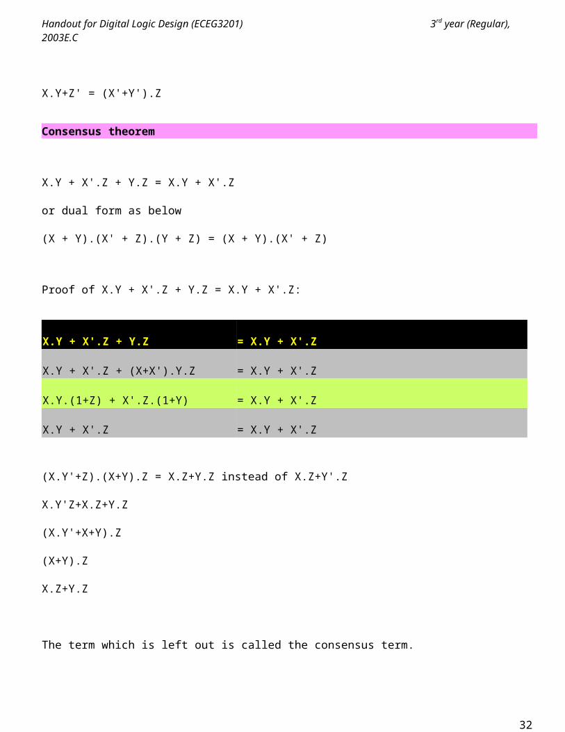
Consensus theorem
X.Y + X'.Z + Y.Z = X.Y + X'.Z
or dual form as below
(X + Y).(X' + Z).(Y + Z) = (X + Y).(X' + Z)
Proof of X.Y + X'.Z + Y.Z = X.Y + X'.Z:
X.Y + X'.Z + Y.Z = X.Y + X'.Z
X.Y + X'.Z + (X+X').Y.Z = X.Y + X'.Z
X.Y.(1+Z) + X'.Z.(1+Y) = X.Y + X'.Z
X.Y + X'.Z = X.Y + X'.Z
(X.Y'+Z).(X+Y).Z = X.Z+Y.Z instead of X.Z+Y'.Z
X.Y'Z+X.Z+Y.Z
(X.Y'+X+Y).Z
(X+Y).Z
X.Z+Y.Z
26
Handout for Digital Logic Design (ECEG3201) 3rd year (Regular), 2003E.C
The term which is left out is called the consensus term.
Given a pair of terms for which a variable appears in one term, and its complement in the other, then the consensus term is formed by ANDing the original terms together, leaving out the selected variable and its complement.
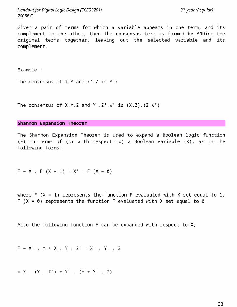
Example :
The consensus of X.Y and X'.Z is Y.Z
The consensus of X.Y.Z and Y'.Z'.W' is (X.Z).(Z.W')
Shannon Expansion Theorem
The Shannon Expansion Theorem is used to expand a Boolean logic function (F) in terms of (or with respect to) a Boolean variable (X), as in the following forms.
F = X . F (X = 1) + X' . F (X = 0)
where F (X = 1) represents the function F evaluated with X set equal to 1; F (X = 0) represents the function F evaluated with X set equal to 0.
Also the following function F can be expanded with respect to X,
F = X' . Y + X . Y . Z' + X' . Y' . Z
= X . (Y . Z') + X' . (Y + Y' . Z)
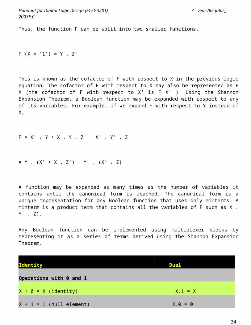
Thus, the function F can be split into two smaller functions.
27
Handout for Digital Logic Design (ECEG3201) 3rd year (Regular), 2003E.C
F (X = '1') = Y . Z'
This is known as the cofactor of F with respect to X in the previous logic equation. The cofactor of F with respect to X may also be represented as F X (the cofactor of F with respect to X' is F X' ). Using the Shannon Expansion Theorem, a Boolean function may be expanded with respect to any of its variables. For example, if we expand F with respect to Y instead of X,
F = X' . Y + X . Y . Z' + X' . Y' . Z
= Y . (X' + X . Z') + Y' . (X' . Z)
A function may be expanded as many times as the number of variables it contains until the canonical form is reached. The canonical form is a unique representation for any Boolean function that uses only minterms. A minterm is a product term that contains all the variables of F such as X . Y' . Z).
Any Boolean function can be implemented using multiplexer blocks by representing it as a series of terms derived using the Shannon Expansion Theorem.
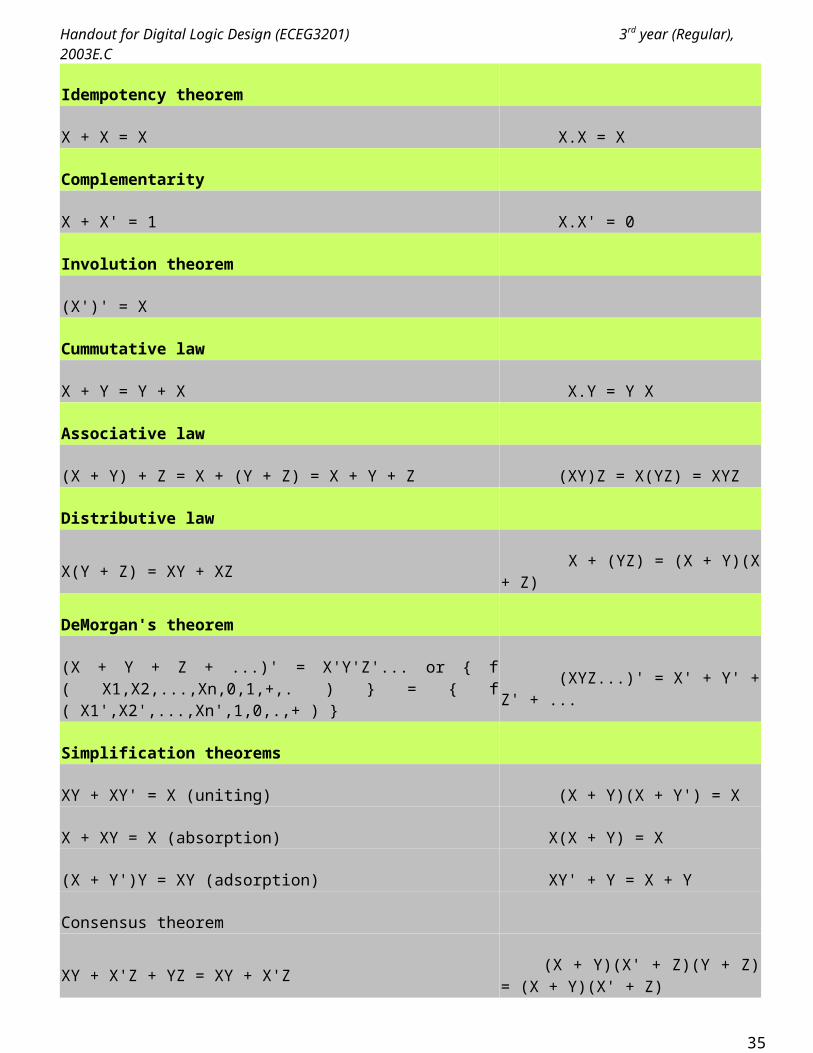
Identity Dual
Operations with 0 and 1
X + 0 = X (identity) X.1 = X
X + 1 = 1 (null element) X.0 = 0
Idempotency theorem
X + X = X X.X = X
Complementarity
X + X' = 1 X.X' = 0
Involution theorem
(X')' = X
Cummutative law
28
Handout for Digital Logic Design (ECEG3201) 3rd year (Regular), 2003E.C
X + Y = Y + X X.Y = Y X
Associative law
(X + Y) + Z = X + (Y + Z) = X + Y + Z (XY)Z = X(YZ) = XYZ
Distributive law
X(Y + Z) = XY + XZ X + (YZ) = (X + Y)(X + Z)
DeMorgan's theorem
(X + Y + Z + ...)' = X'Y'Z'... or { f ( X1,X2,...,Xn,0,1,+,. ) } = { f ( X1',X2',...,Xn',1,0,.,+ ) }
(XYZ...)' = X' + Y' + Z' + ...
Simplification theorems
XY + XY' = X (uniting) (X + Y)(X + Y') = X
X + XY = X (absorption) X(X + Y) = X
(X + Y')Y = XY (adsorption) XY' + Y = X + Y
Consensus theorem
XY + X'Z + YZ = XY + X'Z (X + Y)(X' + Z)(Y + Z) = (X + Y)(X' + Z)
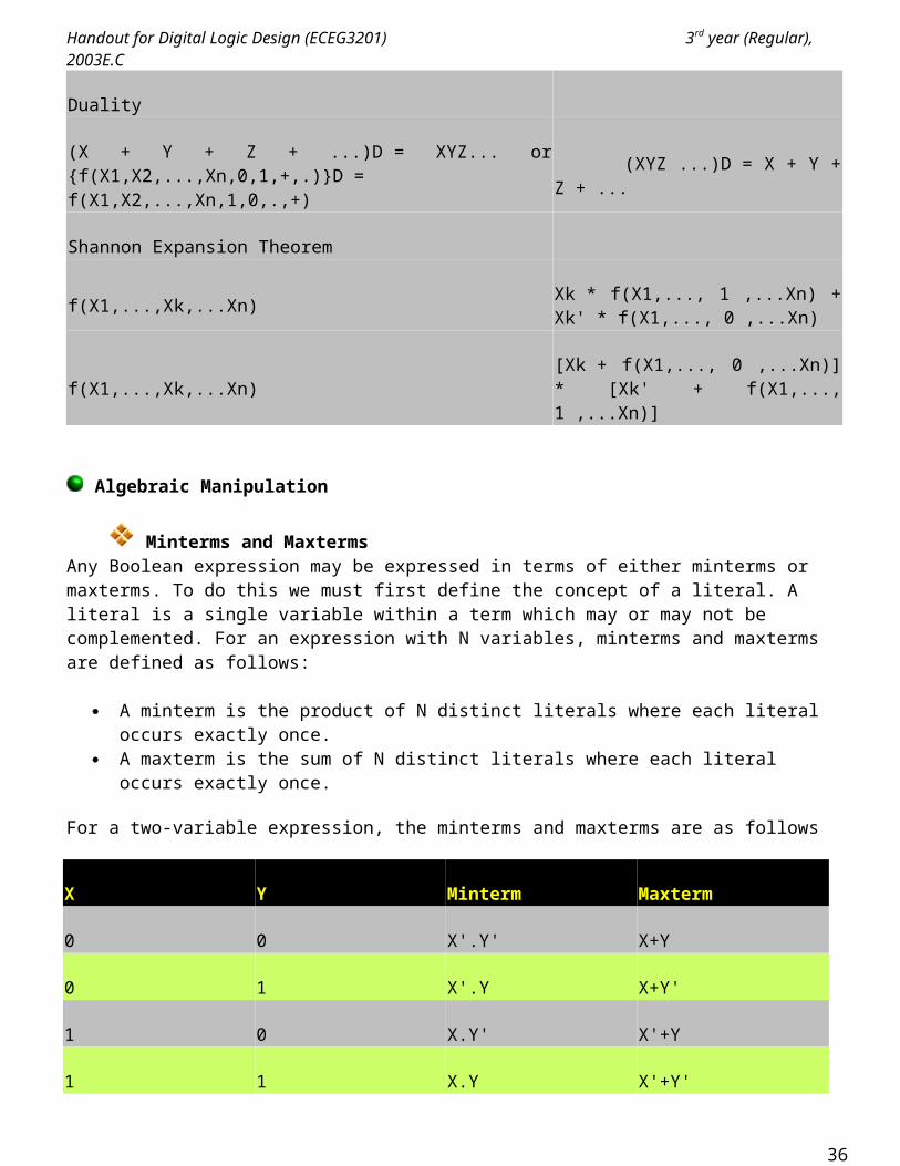
Duality
(X + Y + Z + ...)D = XYZ... or {f(X1,X2,...,Xn,0,1,+,.)}D = f(X1,X2,...,Xn,1,0,.,+)
(XYZ ...)D = X + Y + Z + ...
Shannon Expansion Theorem
f(X1,...,Xk,...Xn)Xk * f(X1,..., 1 ,...Xn) + Xk' * f(X1,..., 0 ,...Xn)
f(X1,...,Xk,...Xn)[Xk + f(X1,..., 0 ,...Xn)] * [Xk' + f(X1,..., 1 ,...Xn)]
Algebraic Manipulation
Minterms and MaxtermsAny Boolean expression may be expressed in terms of either minterms or maxterms. To do this we must first define the concept of a literal. A literal is a single variable within a term which may or may not be complemented. For an expression with N variables, minterms and maxterms are defined as follows:
29
Handout for Digital Logic Design (ECEG3201) 3rd year (Regular), 2003E.C
A minterm is the product of N distinct literals where each literal occurs exactly once. A maxterm is the sum of N distinct literals where each literal occurs exactly once.
For a two-variable expression, the minterms and maxterms are as follows
X Y Minterm Maxterm
0 0 X'.Y' X+Y
0 1 X'.Y X+Y'
1 0 X.Y' X'+Y
1 1 X.Y X'+Y'
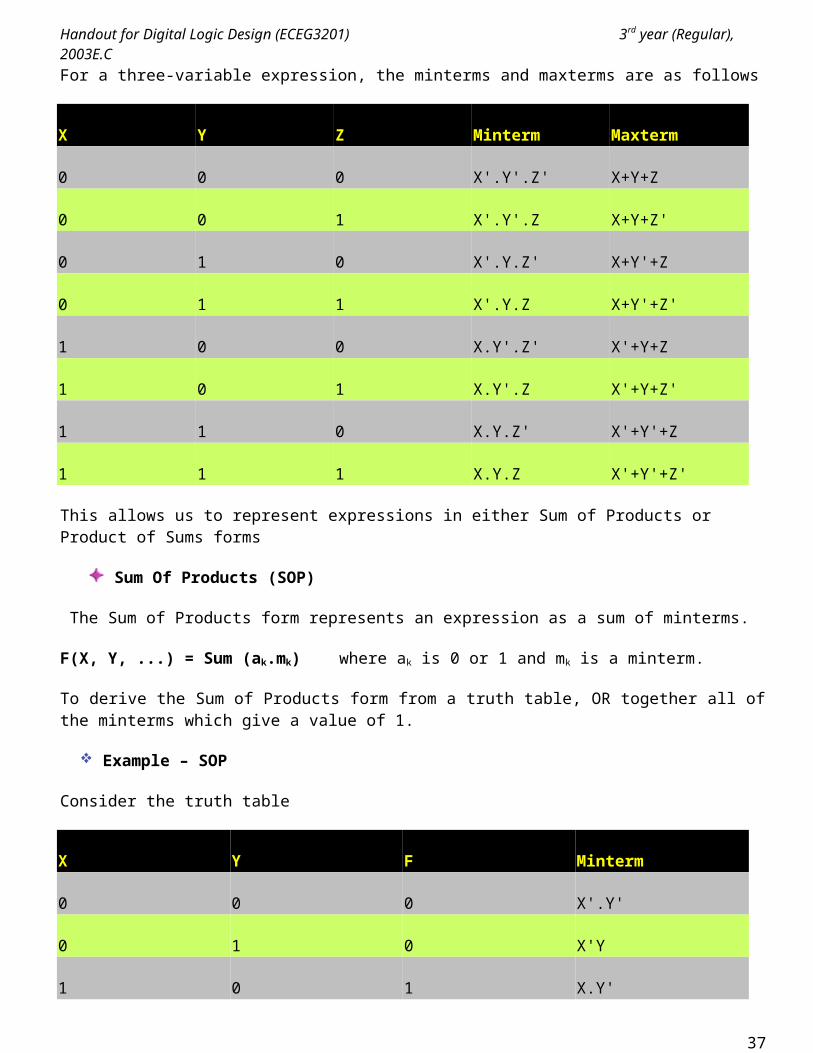
For a three-variable expression, the minterms and maxterms are as follows
X Y Z Minterm Maxterm
0 0 0 X'.Y'.Z' X+Y+Z
0 0 1 X'.Y'.Z X+Y+Z'
0 1 0 X'.Y.Z' X+Y'+Z
0 1 1 X'.Y.Z X+Y'+Z'
1 0 0 X.Y'.Z' X'+Y+Z
1 0 1 X.Y'.Z X'+Y+Z'
1 1 0 X.Y.Z' X'+Y'+Z
1 1 1 X.Y.Z X'+Y'+Z'
This allows us to represent expressions in either Sum of Products or Product of Sums forms
Sum Of Products (SOP)
The Sum of Products form represents an expression as a sum of minterms.
F(X, Y, ...) = Sum (ak.mk) where ak is 0 or 1 and mk is a minterm.
To derive the Sum of Products form from a truth table, OR together all of the minterms which give a value of 1.
Example – SOP
30
Handout for Digital Logic Design (ECEG3201) 3rd year (Regular), 2003E.C
Consider the truth table
X Y F Minterm
0 0 0 X'.Y'
0 1 0 X'Y
1 0 1 X.Y'
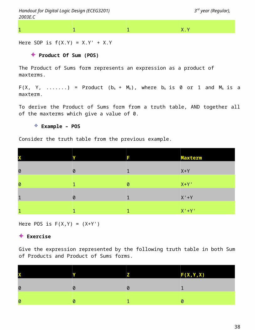
1 1 1 X.Y
Here SOP is f(X.Y) = X.Y' + X.Y
Product Of Sum (POS)
The Product of Sums form represents an expression as a product of maxterms.
F(X, Y, .......) = Product (bk + Mk), where bk is 0 or 1 and Mk is a maxterm.
To derive the Product of Sums form from a truth table, AND together all of the maxterms which give a value of 0.
Example – POS
Consider the truth table from the previous example.
X Y F Maxterm
0 0 1 X+Y
0 1 0 X+Y'
1 0 1 X'+Y
1 1 1 X'+Y'
Here POS is F(X,Y) = (X+Y')
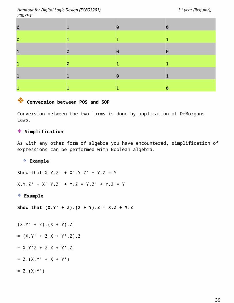
Exercise
Give the expression represented by the following truth table in both Sum of Products and Product of Sums forms.
X Y Z F(X,Y,X)
0 0 0 1
31
Handout for Digital Logic Design (ECEG3201) 3rd year (Regular), 2003E.C
0 0 1 0
0 1 0 0
0 1 1 1
1 0 0 0
1 0 1 1
1 1 0 1
1 1 1 0
Conversion between POS and SOP
Conversion between the two forms is done by application of DeMorgans Laws.
Simplification
As with any other form of algebra you have encountered, simplification of expressions can be performed with Boolean algebra.
Example
Show that X.Y.Z' + X'.Y.Z' + Y.Z = Y
X.Y.Z' + X'.Y.Z' + Y.Z = Y.Z' + Y.Z = Y
Example
Show that (X.Y' + Z).(X + Y).Z = X.Z + Y.Z
(X.Y' + Z).(X + Y).Z
= (X.Y' + Z.X + Y'.Z).Z
= X.Y'Z + Z.X + Y'.Z
= Z.(X.Y' + X + Y')
= Z.(X+Y')
Logic Circuits
32
Handout for Digital Logic Design (ECEG3201) 3rd year (Regular), 2003E.C
Boolean algebra is ideal for expressing the behavior of logic circuits.
A circuit can be expressed as a logic design and implemented as a collection of individual connected logic gates.
Fixed Logic SystemsA fixed logic system has two possible choices for representing true and false.
Positive LogicIn a positive logic system, a high voltage is used to represent logical true (1), and a low voltage for a logical false (0). Negative LogicIn a negative logic system, a low voltage is used to represent logical true (1), and a high voltage for a logical false (0).
In positive logic circuits it is normal to use +5V for true and 0V for false.
Switching Circuits
The abstract logic described previously can be implemented as an actual circuit. Switches are left open for logic 0 and closed for logic 1.
Two variable AND circuit X.Y
Two variable OR circuit X + Y
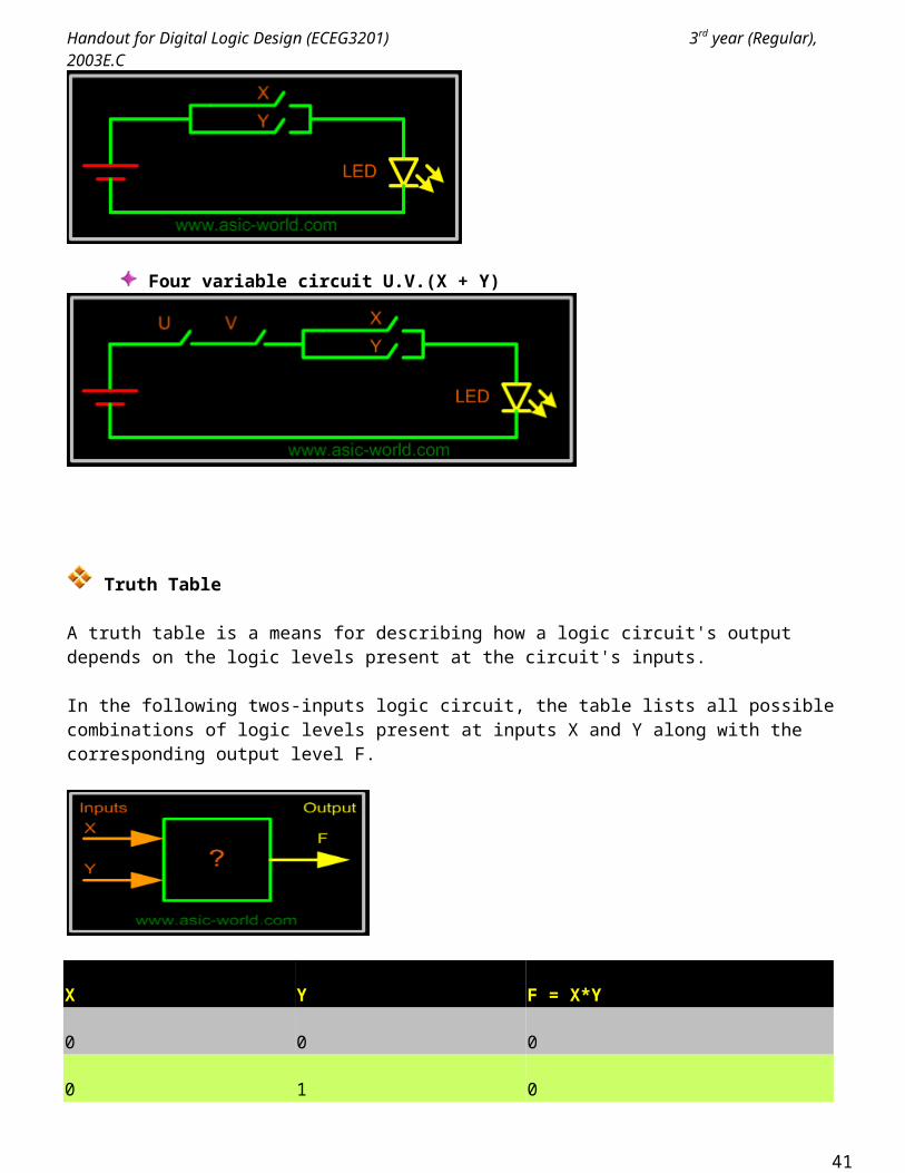
Four variable circuit U.V.(X + Y)
33
Handout for Digital Logic Design (ECEG3201) 3rd year (Regular), 2003E.C
Truth Table
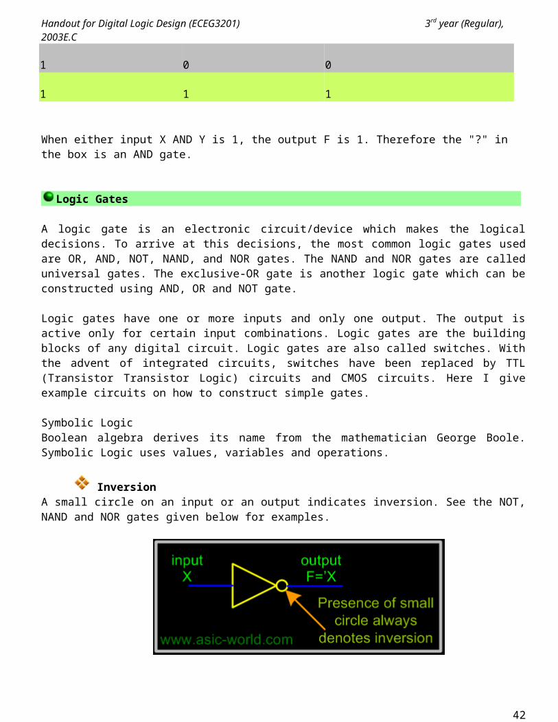
A truth table is a means for describing how a logic circuit's output depends on the logic levels present at the circuit's inputs.
In the following twos-inputs logic circuit, the table lists all possible combinations of logic levels present at inputs X and Y along with the corresponding output level F.
X Y F = X*Y
0 0 0
0 1 0
1 0 0
1 1 1
When either input X AND Y is 1, the output F is 1. Therefore the "?" in the box is an AND gate.
Logic Gates
A logic gate is an electronic circuit/device which makes the logical decisions. To arrive at this decisions, the most common logic gates used are OR, AND, NOT, NAND, and NOR gates. The NAND and NOR gates are called universal gates. The exclusive-OR gate is another logic gate which can be constructed using AND, OR and NOT gate.
34
Handout for Digital Logic Design (ECEG3201) 3rd year (Regular), 2003E.C
Logic gates have one or more inputs and only one output. The output is active only for certain input combinations. Logic gates are the building blocks of any digital circuit. Logic gates are also called switches. With the advent of integrated circuits, switches have been replaced by TTL (Transistor Transistor Logic) circuits and CMOS circuits. Here I give example circuits on how to construct simple gates.
Symbolic LogicBoolean algebra derives its name from the mathematician George Boole. Symbolic Logic uses values, variables and operations.
InversionA small circle on an input or an output indicates inversion. See the NOT, NAND and NOR gates given below for examples.
Multiple Input GatesGiven commutative and associative laws, many logic gates can be implemented with more than two inputs, and for reasons of space in circuits, usually multiple input, complex gates are made. You will encounter such gates in real world.
Gates Types
AND OR NOT BUF NAND NOR XOR XNOR
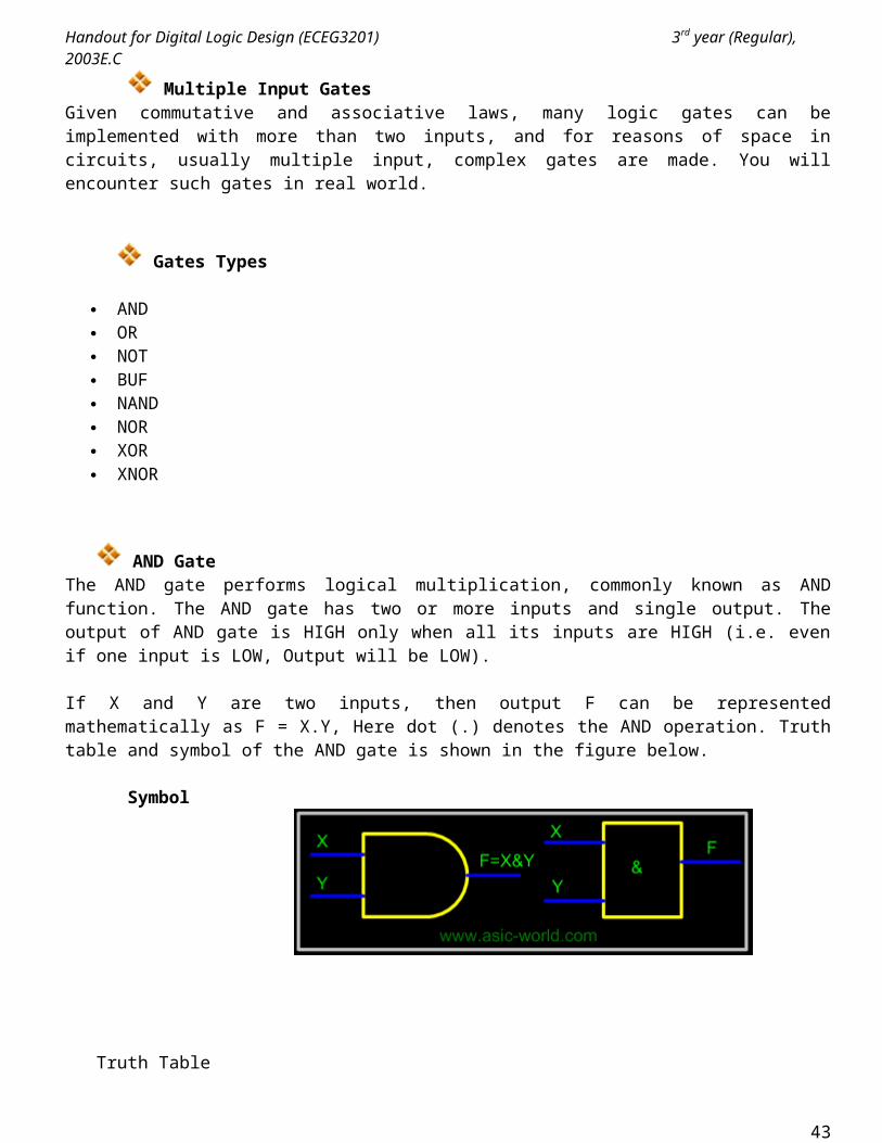
AND GateThe AND gate performs logical multiplication, commonly known as AND function. The AND gate has two or more inputs and single output. The output of AND gate is HIGH only when all its inputs are HIGH (i.e. even if one input is LOW, Output will be LOW).
If X and Y are two inputs, then output F can be represented mathematically as F = X.Y, Here dot (.) denotes the AND operation. Truth table and symbol of the AND gate is shown in the figure below.
35
Handout for Digital Logic Design (ECEG3201) 3rd year (Regular), 2003E.C
Symbol
Truth Table
X Y F=(X.Y)
0 0 0
0 1 0
1 0 0
1 1 1
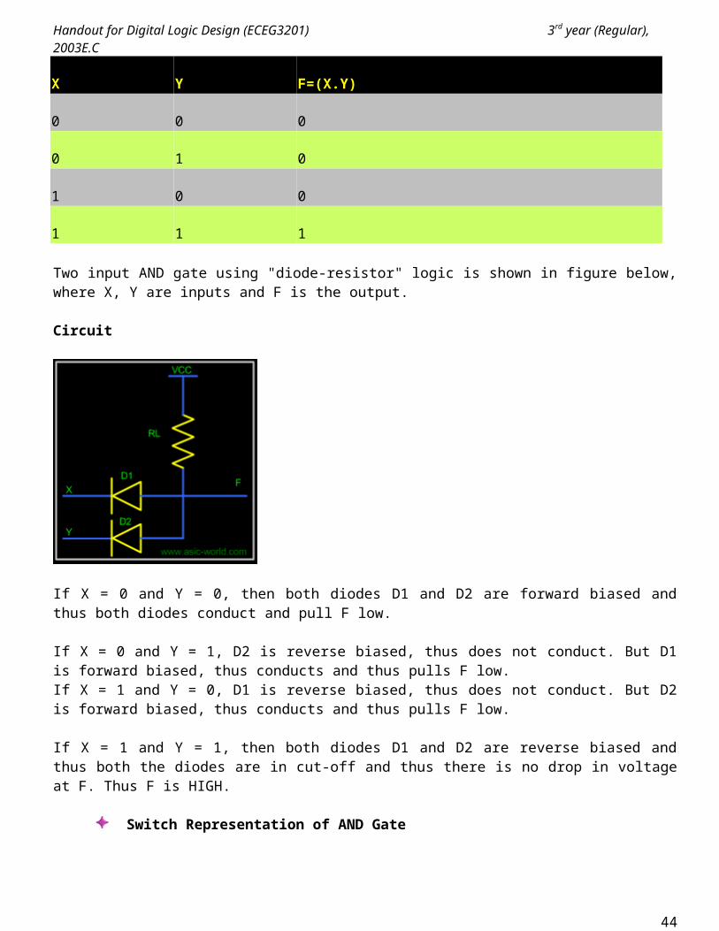
Two input AND gate using "diode-resistor" logic is shown in figure below, where X, Y are inputs and F is the output.
Circuit
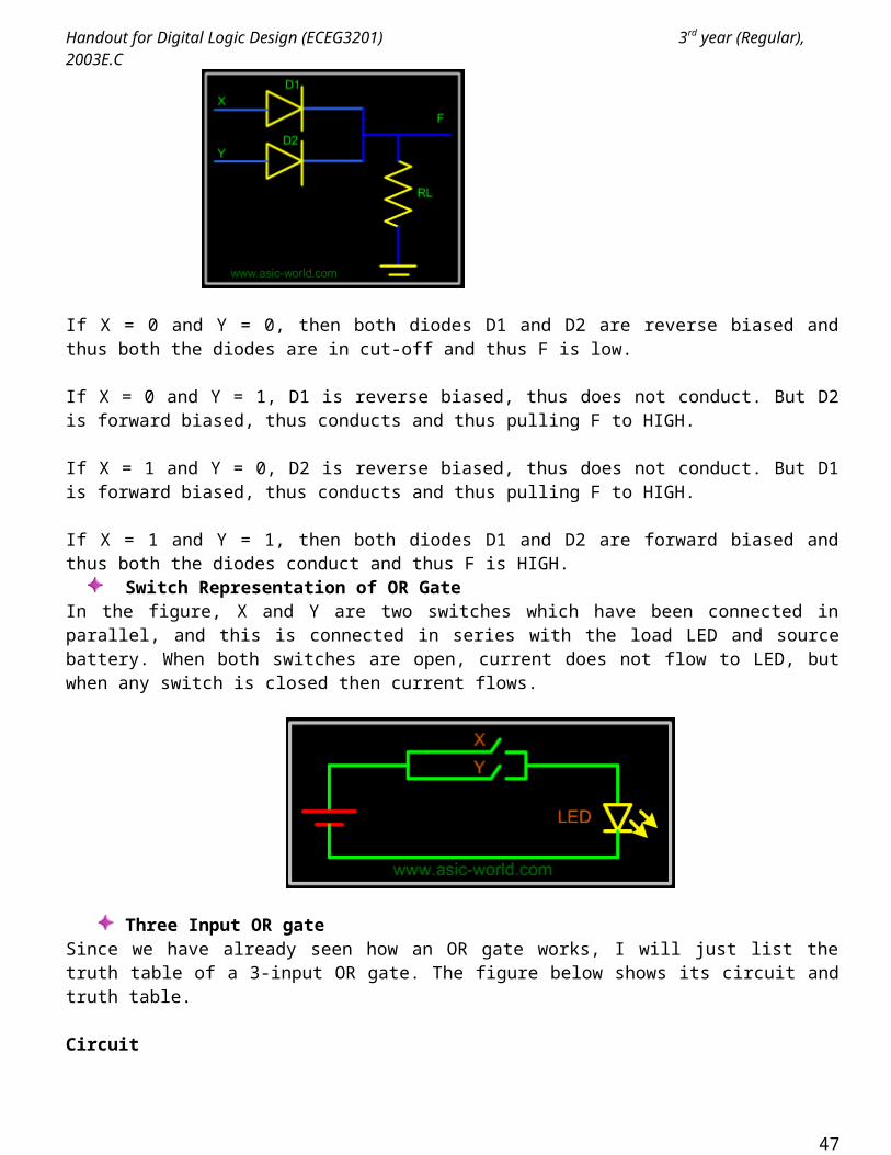
If X = 0 and Y = 0, then both diodes D1 and D2 are forward biased and thus both diodes conduct and pull F low.
If X = 0 and Y = 1, D2 is reverse biased, thus does not conduct. But D1 is forward biased, thus conducts and thus pulls F low.If X = 1 and Y = 0, D1 is reverse biased, thus does not conduct. But D2 is forward biased, thus conducts and thus pulls F low.
36
Handout for Digital Logic Design (ECEG3201) 3rd year (Regular), 2003E.C
If X = 1 and Y = 1, then both diodes D1 and D2 are reverse biased and thus both the diodes are in cut-off and thus there is no drop in voltage at F. Thus F is HIGH.
Switch Representation of AND Gate
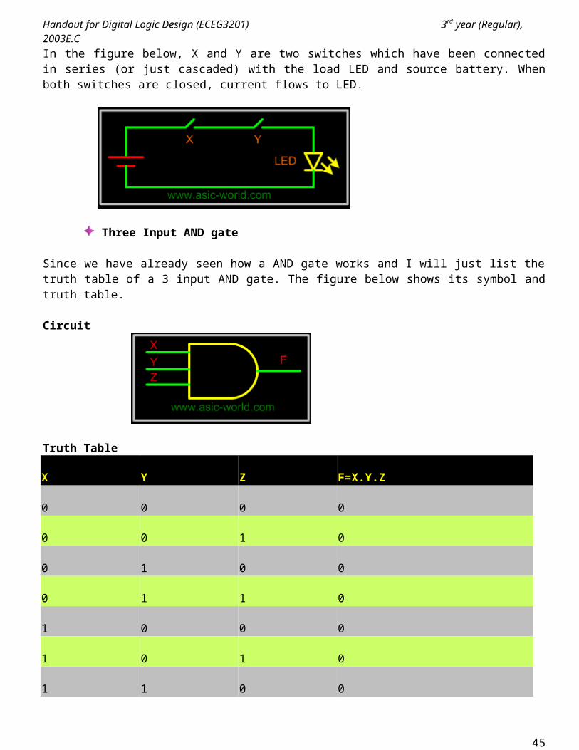
In the figure below, X and Y are two switches which have been connected in series (or just cascaded) with the load LED and source battery. When both switches are closed, current flows to LED.
Three Input AND gate
Since we have already seen how a AND gate works and I will just list the truth table of a 3 input AND gate. The figure below shows its symbol and truth table.
Circuit
Truth Table
X Y Z F=X.Y.Z
0 0 0 0
0 0 1 0
0 1 0 0
0 1 1 0
1 0 0 0
1 0 1 0
1 1 0 0
1 1 1 1
37
Handout for Digital Logic Design (ECEG3201) 3rd year (Regular), 2003E.C
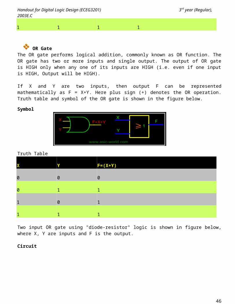
OR GateThe OR gate performs logical addition, commonly known as OR function. The OR gate has two or more inputs and single output. The output of OR gate is HIGH only when any one of its inputs are HIGH (i.e. even if one input is HIGH, Output will be HIGH).
If X and Y are two inputs, then output F can be represented mathematically as F = X+Y. Here plus sign (+) denotes the OR operation. Truth table and symbol of the OR gate is shown in the figure below.
Symbol
Truth Table
X Y F=(X+Y)
0 0 0
0 1 1
1 0 1
1 1 1
Two input OR gate using "diode-resistor" logic is shown in figure below, where X, Y are inputs and F is the output.
Circuit
If X = 0 and Y = 0, then both diodes D1 and D2 are reverse biased and thus both the diodes are in cut-off and thus F is low.
If X = 0 and Y = 1, D1 is reverse biased, thus does not conduct. But D2 is forward biased, thus conducts and thus pulling F to HIGH.
38
Handout for Digital Logic Design (ECEG3201) 3rd year (Regular), 2003E.C
If X = 1 and Y = 0, D2 is reverse biased, thus does not conduct. But D1 is forward biased, thus conducts and thus pulling F to HIGH.
If X = 1 and Y = 1, then both diodes D1 and D2 are forward biased and thus both the diodes conduct and thus F is HIGH. Switch Representation of OR GateIn the figure, X and Y are two switches which have been connected in parallel, and this is connected in series with the load LED and source battery. When both switches are open, current does not flow to LED, but when any switch is closed then current flows.
Three Input OR gateSince we have already seen how an OR gate works, I will just list the truth table of a 3-input OR gate. The figure below shows its circuit and truth table.
Circuit
Truth Table
X Y Z F=X+Y+Z
0 0 0 0
0 0 1 1
0 1 0 1
0 1 1 1
1 0 0 1
1 0 1 1
1 1 0 1
1 1 1 1
NOT Gate
39
Handout for Digital Logic Design (ECEG3201) 3rd year (Regular), 2003E.C
The NOT gate performs the basic logical function called inversion or complementation. NOT gate is also called inverter. The purpose of this gate is to convert one logic level into the opposite logic level. It has one input and one output. When a HIGH level is applied to an inverter, a LOW level appears on its output and vice versa.
If X is the input, then output F can be represented mathematically as F = X', Here apostrophe (') denotes the NOT (inversion) operation. There are a couple of other ways to represent inversion, F= !X, here ! represents inversion. Truth table and NOT gate symbol is shown in the figure below.
Symbol
Truth Table
X Y=X'
0 1
1 0
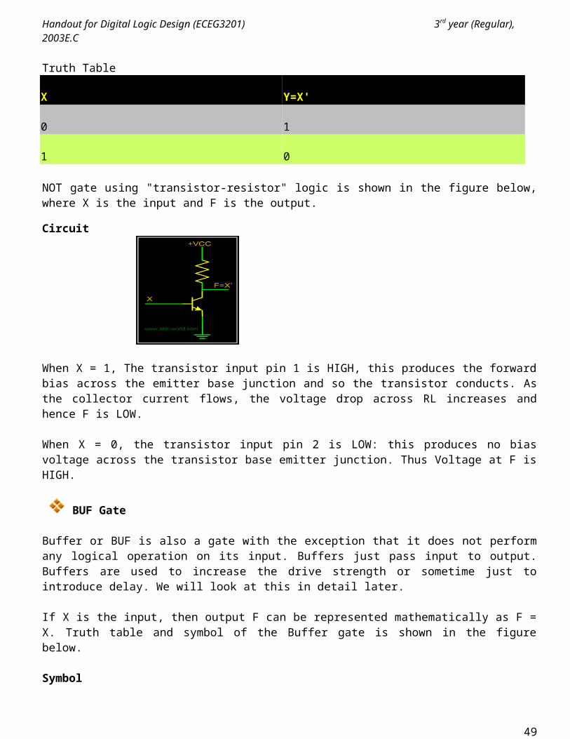
NOT gate using "transistor-resistor" logic is shown in the figure below, where X is the input and F is the output.
Circuit
When X = 1, The transistor input pin 1 is HIGH, this produces the forward bias across the emitter base junction and so the transistor conducts. As the collector current flows, the voltage drop across RL increases and hence F is LOW.
When X = 0, the transistor input pin 2 is LOW: this produces no bias voltage across the transistor base emitter junction. Thus Voltage at F is HIGH.
BUF Gate
40
Handout for Digital Logic Design (ECEG3201) 3rd year (Regular), 2003E.C
Buffer or BUF is also a gate with the exception that it does not perform any logical operation on its input. Buffers just pass input to output. Buffers are used to increase the drive strength or sometime just to introduce delay. We will look at this in detail later.
If X is the input, then output F can be represented mathematically as F = X. Truth table and symbol of the Buffer gate is shown in the figure below.
Symbol
X Y=X
0 0
1 1
NAND Gate
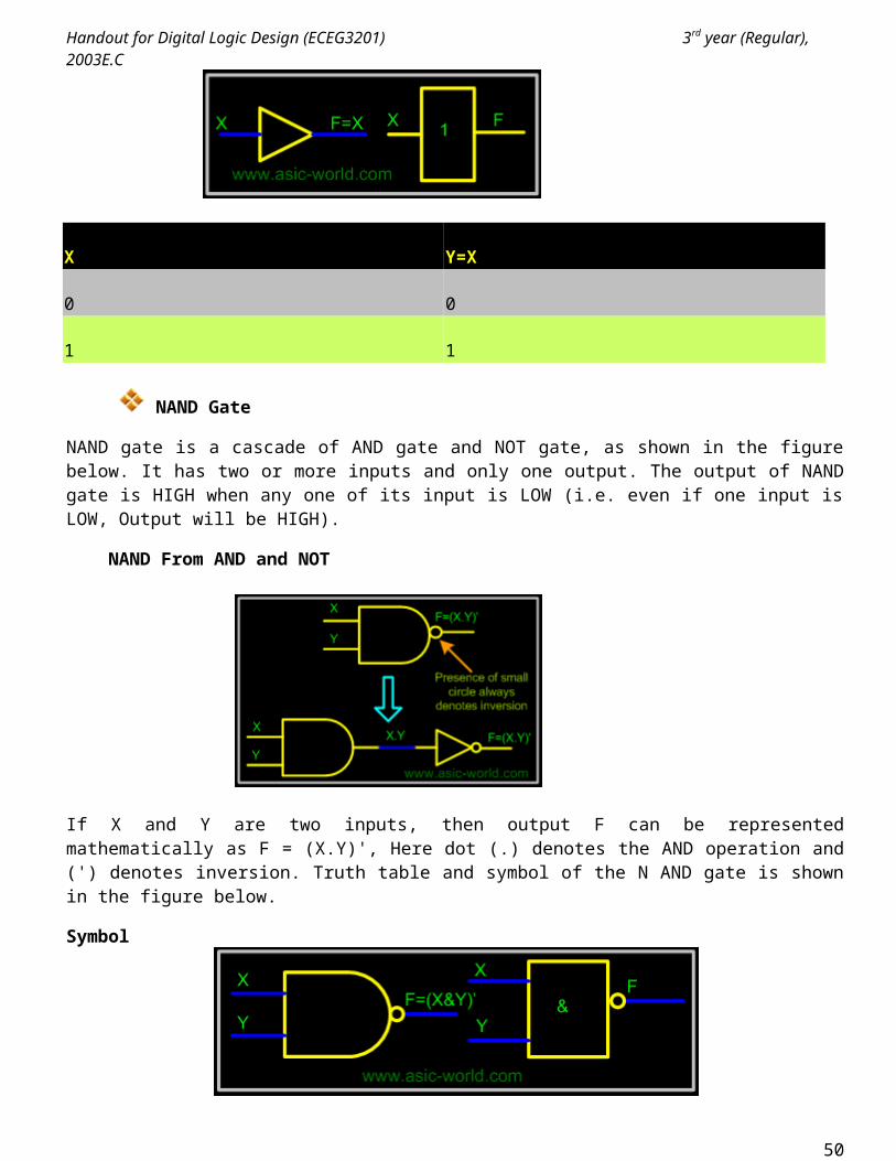
NAND gate is a cascade of AND gate and NOT gate, as shown in the figure below. It has two or more inputs and only one output. The output of NAND gate is HIGH when any one of its input is LOW (i.e. even if one input is LOW, Output will be HIGH).
NAND From AND and NOT
If X and Y are two inputs, then output F can be represented mathematically as F = (X.Y)', Here dot (.) denotes the AND operation and (') denotes inversion. Truth table and symbol of the N AND gate is shown in the figure below.
Symbol
41
Handout for Digital Logic Design (ECEG3201) 3rd year (Regular), 2003E.C
Truth Table
X Y F=(X.Y)'
0 0 1
0 1 1
1 0 1
1 1 0
NOR GateNOR gate is a cascade of OR gate and NOT gate, as shown in the figure below. It has two or more inputs and only one output. The output of NOR gate is HIGH when any all its inputs are LOW (i.e. even if one input is HIGH, output will be LOW).
Symbol
If X and Y are two inputs, then output F can be represented mathematically as F = (X+Y)'; here plus (+) denotes the OR operation and (') denotes inversion. Truth table and symbol of the NOR gate is shown in the figure below.
Truth Table
X Y F=(X+Y)'
0 0 1
0 1 0
1 0 0
1 1 0
XOR Gate
42
Handout for Digital Logic Design (ECEG3201) 3rd year (Regular), 2003E.C
An Exclusive-OR (XOR) gate is gate with two or three or more inputs and one output. The output of a two-input XOR gate assumes a HIGH state if one and only one input assumes a HIGH state. This is equivalent to saying that the output is HIGH if either input X or input Y is HIGH exclusively, and LOW when both are 1 or 0 simultaneously.
If X and Y are two inputs, then output F can be represented mathematically as F = X Y, Here denotes the XOR operation. X Y and is equivalent to X.Y' + X'.Y. Truth table and symbol of the XOR gate is shown in the figure below.
XOR From Simple gates
Symbol
Truth Table
X Y F=(X Y)
0 0 0
0 1 1
1 0 1
1 1 0
XNOR GateAn Exclusive-NOR (XNOR) gate is gate with two or three or more inputs and one output. The output of a two-input XNOR gate assumes a HIGH state if all the inputs assumes same state. This is equivalent to saying that the output is HIGH if both input X and input Y is HIGH exclusively or same as input X and input Y is LOW exclusively, and LOW when both are not same.
If X and Y are two inputs, then output F can be represented mathematically as F = X Y, Here denotes the XNOR operation. X Y and is equivalent to X.Y + X'.Y'. Truth table and symbol of the XNOR gate is shown in the figure below.
Symbol
43
Handout for Digital Logic Design (ECEG3201) 3rd year (Regular), 2003E.C
Truth Table
X Y F=(X Y)'
0 0 1
0 1 0
1 0 0
1 1 1
Universal GatesUniversal gates are the ones which can be used for implementing any gate like AND, OR and NOT, or any combination of these basic gates; NAND and NOR gates are universal gates. But there are some rules that need to be followed when implementing NAND or NOR based gates.
To facilitate the conversion to NAND and NOR logic, we have two new graphic symbols for these gates.
NAND Gate
NOR Gate
Realization of logic function using NAND gatesAny logic function can be implemented using NAND gates. To achieve this, first the logic function has to be written in Sum of Product (SOP) form. Once logic function is converted to SOP, then is very easy to implement using NAND gate. In other words any logic circuit with AND gates in first level and OR gates in second level can be converted into a NAND-NAND gate circuit.
Consider the following SOP expression
44
Handout for Digital Logic Design (ECEG3201) 3rd year (Regular), 2003E.C
F = W.X.Y + X.Y.Z + Y.Z.W
The above expression can be implemented with three AND gates in first stage and one OR gate in second stage as shown in figure.
If bubbles are introduced at AND gates output and OR gates inputs (the same for NOR gates), the above circuit becomes as shown in figure.
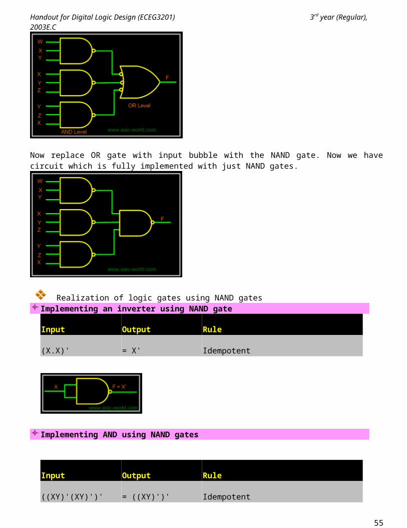
Now replace OR gate with input bubble with the NAND gate. Now we have circuit which is fully implemented with just NAND gates.
Realization of logic gates using NAND gatesImplementing an inverter using NAND gate
45
Handout for Digital Logic Design (ECEG3201) 3rd year (Regular), 2003E.C
Input Output Rule
(X.X)' = X' Idempotent
Implementing AND using NAND gates
Input Output Rule
((XY)'(XY)')' = ((XY)')' Idempotent
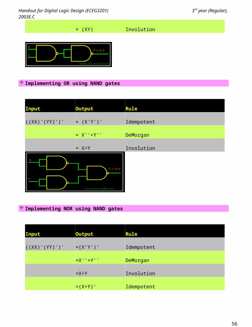
= (XY) Involution
Implementing OR using NAND gates
Input Output Rule
((XX)'(YY)')' = (X'Y')' Idempotent
= X''+Y'' DeMorgan
= X+Y Involution
Implementing NOR using NAND gates
46
Handout for Digital Logic Design (ECEG3201) 3rd year (Regular), 2003E.C
Input Output Rule
((XX)'(YY)')' =(X'Y')' Idempotent
=X''+Y'' DeMorgan
=X+Y Involution
=(X+Y)' Idempotent
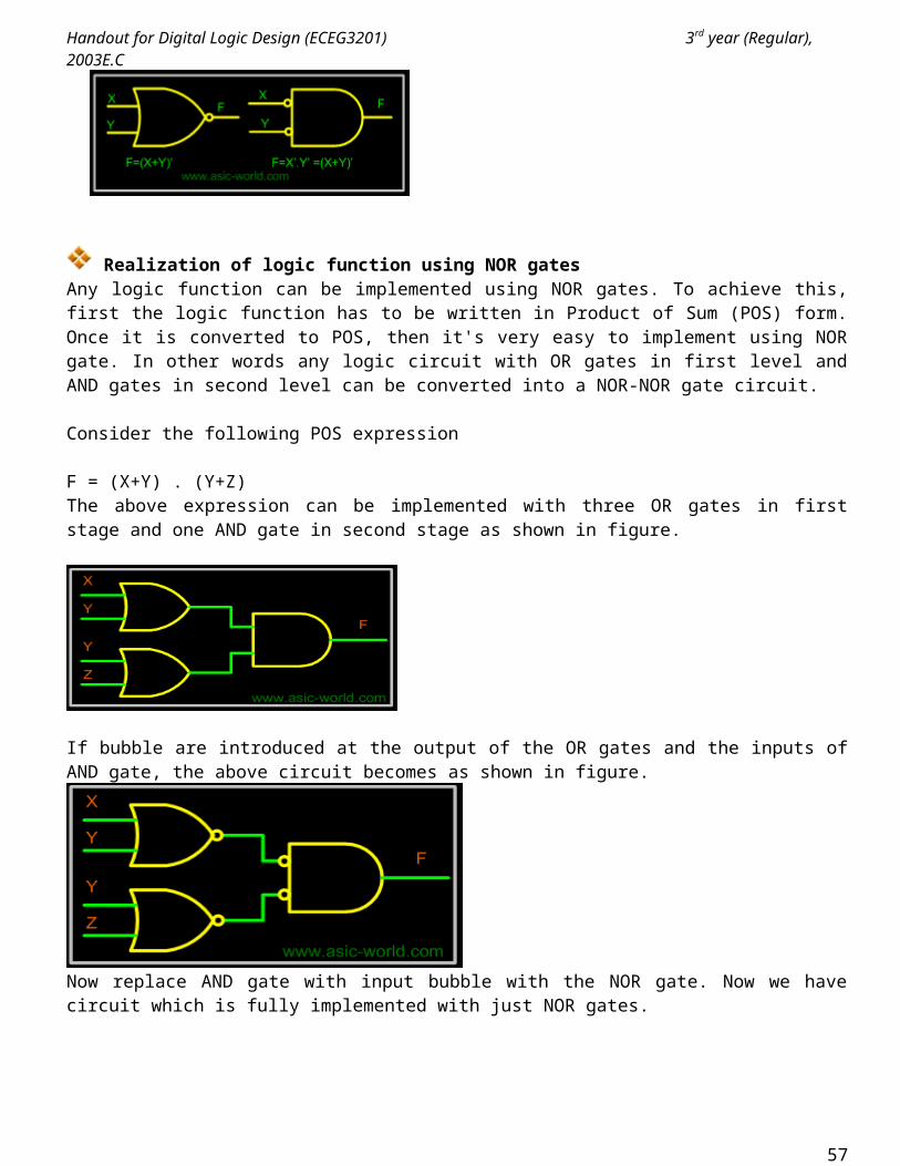
Realization of logic function using NOR gatesAny logic function can be implemented using NOR gates. To achieve this, first the logic function has to be written in Product of Sum (POS) form. Once it is converted to POS, then it's very easy to implement using NOR gate. In other words any logic circuit with OR gates in first level and AND gates in second level can be converted into a NOR-NOR gate circuit.
Consider the following POS expression
F = (X+Y) . (Y+Z)The above expression can be implemented with three OR gates in first stage and one AND gate in second stage as shown in figure.
If bubble are introduced at the output of the OR gates and the inputs of AND gate, the above circuit becomes as shown in figure.
47
Handout for Digital Logic Design (ECEG3201) 3rd year (Regular), 2003E.C
Now replace AND gate with input bubble with the NOR gate. Now we have circuit which is fully implemented with just NOR gates.
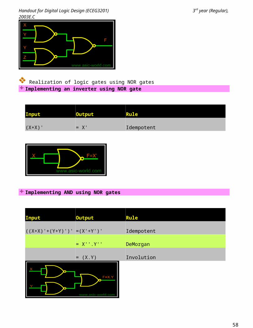
Realization of logic gates using NOR gatesImplementing an inverter using NOR gate
Input Output Rule
(X+X)' = X' Idempotent
Implementing AND using NOR gates
Input Output Rule
((X+X)'+(Y+Y)')' =(X'+Y')' Idempotent
= X''.Y'' DeMorgan
= (X.Y) Involution
48
Handout for Digital Logic Design (ECEG3201) 3rd year (Regular), 2003E.C
Implementing OR using NOR gates
Input Output Rule
((X+Y)'+(X+Y)')' = ((X+Y)')' Idempotent
= X+Y Involution
Implementing NAND using NOR gates
Input Output Rule
((X+Y)'+(X+Y)')' = ((X+Y)')' Idempotent
= X+Y Involution
= (X+Y)' Idempotent
49
Handout for Digital Logic Design (ECEG3201) 3rd year (Regular), 2003E.C
Chapter 3 Combinational logic design
IntroductionSimplification of Boolean functions is mainly used to reduce the gate count of a design. Less number of gates means less power consumption, sometimes the circuit works faster and also when number of gates is reduced, cost also comes down.
There are many ways to simplify a logic design, some of them are given below. We will be looking at each of these in detail in the next few pages.
Algebraic Simplification.o Simplify symbolically using theorems/postulates.o Requires good skills
Karnaugh Maps.o Diagrammatic technique using 'Venn-like diagram.o Limited to no more than 6 variables.
We have already seen how Algebraic Simplification works, so lets concentrate on Karnaugh Maps or simply k-maps.
Karnaugh Maps
Karnaugh maps provide a systematic method to obtain simplified sum-of-products (SOPs) Boolean expressions. This is a compact way of representing a truth table and is a technique that is used to simplify logic expressions. It is ideally suited for four or less variables, becoming cumbersome for five or more variables. Each square represents either a minterm or maxterm. A K-map of n variables will have 2 squares. For a Boolean expression, product terms are denoted by 1's, while sum terms are denoted by 0's - but 0's are often left blank.
50
Handout for Digital Logic Design (ECEG3201) 3rd year (Regular), 2003E.C
A K-map consists of a grid of squares, each square representing one canonical minterm combination of the variables or their inverse. The map is arranged so that squares representing minterms which differ by only one variable are adjacent both vertically and horizontally. Therefore XY'Z' would be adjacent to X'Y'Z' and would also adjacent to XY'Z and XYZ'.
Minimization Technique
Based on the Unifying Theorem: X + X' = 1 The expression to be minimized should generally be in sum-of-product form (If necessary, the
conversion process is applied to create the sum-of-product form). The function is mapped onto the K-map by marking a 1 in those squares corresponding to the terms in
the expression to be simplified (The other squares may be filled with 0's). Pairs of 1's on the map which are adjacent are combined using the theorem Y(X+X') = Y where Y is
any Boolean expression (If two pairs are also adjacent, then these can also be combined using the same theorem).
The minimization procedure consists of recognizing those pairs and multiple pairs.o These are circled indicating reduced terms.o Groups which can be circled are those which have two (21) 1's, four (22) 1's, eight (23) 1's, and
so on.o Note that because squares on one edge of the map are considered adjacent to those on the
opposite edge, group can be formed with these squares.o Groups are allowed to overlap.
The objective is to cover all the 1's on the map in the fewest number of groups and to create the largest groups to do this.
Once all possible groups have been formed, the corresponding terms are identified.o A group of two 1's eliminates one variable from the original minterm.o A group of four 1's eliminates two variables from the original minterm.o A group of eight 1's eliminates three variables from the original minterm, and so on.o The variables eliminated are those which are different in the original minterms of the group.
2-Variable K-Map
In any K-Map, each square represents a minterm. Adjacent squares always differ by just one literal (So that the unifying theorem may apply: X + X' = 1). For the 2-variable case (e.g.: variables X, Y), the map can be drawn as below. Two variable map is the one which has got only two variables as input.
Equivalent labeling
51
Handout for Digital Logic Design (ECEG3201) 3rd year (Regular), 2003E.C
K-map needs not follow the ordering as shown in the figure above. What this means is that we can change the position of m0, m1, m2, m3 of the above figure as shown in the two figures below.Position assignment is the same as the default k-maps positions. This is the one which we will be using throughout this tutorial.
This figure is with changed position of m0, m1, m2, m3.
The K-map for a function is specified by putting a '1' in the square corresponding to a minterm, a '0' otherwise.
Example- Carry and Sum of a half adder
In this example we have the truth table as input, and we have two output functions. Generally we may have n output functions for m input variables. Since we have two output functions, we need to draw two k-maps (i.e. one for each function). Truth table of 1 bit adder is shown below. Draw the k-map for Carry and Sum as shown below.
X Y Sum Carry
0 0 0 0
0 1 1 0
1 0 1 0
1 1 0 1
52
Handout for Digital Logic Design (ECEG3201) 3rd year (Regular), 2003E.C
Grouping/Circling K-maps
The power of K-maps is in minimizing the terms, K-maps can be minimized with the help of grouping the terms to form single terms. When forming groups of squares, observe/consider the following:
Every square containing 1 must be considered at least once. A square containing 1 can be included in as many groups as desired.
A group must be as large as possible.
If a square containing 1 cannot be placed in a group, then leave it out to include in final expression. The number of squares in a group must be equal to 2 , i.e. 2,4,8,. The map is considered to be folded or spherical, therefore squares at the end of a row or column are
treated as adjacent squares. The simplified logic expression obtained from a K-map is not always unique. Groupings can be made
in different ways. Before drawing a K-map the logic expression must be in canonical form.
53
Handout for Digital Logic Design (ECEG3201) 3rd year (Regular), 2003E.C
In the next few pages we will see some examples on grouping.
Example of invalid groups
Example - X'Y+XY
In this example we have the equation as input, and we have one output function. Draw the k-map for function F with marking 1 for X'Y and XY position. Now combine two 1's as shown in figure to form the single term. As you can see X and X' get canceled and only Y remains.
F = Y
54
Handout for Digital Logic Design (ECEG3201) 3rd year (Regular), 2003E.C
Example - X'Y+XY+XY'In this example we have the equation as input, and we have one output function. Draw the k-map for function F with marking 1 for X'Y, XY and XY position. Now combine two 1's as shown in figure to form the two single terms.
F = X + Y
3-Variable K-MapThere are 8 minterms for 3 variables (X, Y, Z). Therefore, there are 8 cells in a 3-variable K-map. One important thing to note is that K-maps follow the gray code sequence, not the binary one.
Using gray code arrangement ensures that minterms of adjacent cells differ by only ONE literal. (Other arrangements which satisfy this criterion may also be used.)
Each cell in a 3-variable K-map has 3 adjacent neighbours. In general, each cell in an n-variable K-map has n adjacent neighbours.
55
Handout for Digital Logic Design (ECEG3201) 3rd year (Regular), 2003E.C
There is wrap-around in the K-map X'Y'Z' (m0) is adjacent to X'YZ' (m2)
XY'Z' (m4) is adjacent to XYZ' (m6)
Example
F = XYZ'+XYZ+X'YZ
F = XY + YZ
Example F(X,Y,Z) = (1,3,4,5,6,7)
56
Handout for Digital Logic Design (ECEG3201) 3rd year (Regular), 2003E.C
F = X + Z
4-Variable K-MapThere are 16 cells in a 4-variable (W, X, Y, Z); K-map as shown in the figure below.
There are 2 wrap-around: a horizontal wrap-around and a vertical wrap-around. Every cell thus has 4 neighbours. For example, the cell corresponding to minterm m0 has neighbours m1, m2, m4 and m8.
Example F(W,X,Y,Z) = (1,5,12,13)
57
Handout for Digital Logic Design (ECEG3201) 3rd year (Regular), 2003E.C
F = WY'Z + W'Y'Z
Example F(W,X,Y,Z) = (4, 5, 10, 11, 14, 15)
F = W'XY' + WY
5-Variable K-MapThere are 32 cells in a 5-variable (V, W, X, Y, Z); K-map as shown in the figure below.
58
Handout for Digital Logic Design (ECEG3201) 3rd year (Regular), 2003E.C
Inverse Function The 0's on a K-map indicate when the function is 0. We can minimize the inverse function by grouping the 0's (and any suitable don't cares) instead of the
1's. This technique leads to an expression which is not logically equivalent to that obtained by grouping
the 1's (i.e., the inverse of X != X'). Minimizing for the inverse function may be particularly advantageous if there are many more 0's than
1's on the map. We can also apply De Morgan's theorem to obtain a product-of-sum expression.
QUINE-McCLUSKEY MINIMIZATION
Quine-McCluskey minimization method uses the same theorem to produce the solution as the K-map method, namely X(Y+Y') =X
Minimization Technique
The expression is represented in the canonical SOP form if not already in that form. The function is converted into numeric notation. The numbers are converted into binary form. The minterms are arranged in a column divided into groups. Begin with the minimization procedure.
o Each minterm of one group is compared with each minterm in the group immediately below.o Each time a number is found in one group which is the same as a number in the group below
except for one digit, the numbers pair is ticked and a new composite is created.o This composite number has the same number of digits as the numbers in the pair except the
digit different which is replaced by an "x". The above procedure is repeated on the second column to generate a third column. The next step is to identify the essential prime implicants, which can be done using a prime implicant
chart.o Where a prime implicant covers a minterm, the intersection of the corresponding row and
column is marked with a cross.o Those columns with only one cross identify the essential prime implicants. -> These prime
implicants must be in the final answer.o The single crosses on a column are circled and all the crosses on the same row are also circled,
indicating that these crosses are covered by the prime implicants selected.o Once one cross on a column is circled, all the crosses on that column can be circled since the
minterm is now covered.o If any non-essential prime implicant has all its crosses circled, the prime implicant is redundant
and need not be considered further. Next, a selection must be made from the remaining nonessential prime implicants, by considering how
the non-circled crosses can be covered best.o One generally would take those prime implicants which cover the greatest number of crosses
on their row.o If all the crosses in one row also occur on another row which includes further crosses, then the
latter is said to dominate the former and can be selected.o The dominated prime implicant can then be deleted.
59
Handout for Digital Logic Design (ECEG3201) 3rd year (Regular), 2003E.C
Example
Find the minimal sum of products for the Boolean expression, f= (1,2,3,7,8,9,10,11,14,15), using Quine-McCluskey method.
Firstly these minterms are represented in the binary form as shown in the table below. The above binary representations are grouped into a number of sections in terms of the number of 1's as shown in the table below.
Binary representation of minterms
Minterms U V W X1 0 0 0 12 0 0 1 03 0 0 1 17 0 1 1 18 1 0 0 09 1 0 0 110 1 0 1 011 1 0 1 114 1 1 1 015 1 1 1 1
Group of minterms for different number of 1's
No of 1's Minterms U V W X1 1 0 0 0 11 2 0 0 1 01 8 1 0 0 02 3 0 0 1 12 9 1 0 0 12 10 1 0 1 03 7 0 1 1 13 11 1 0 1 13 14 1 1 1 04 15 1 1 1 1
Any two numbers in these groups which differ from each other by only one variable can be chosen and combined, to get 2-cell combination, as shown in the table below.
2-Cell combinations
Combinations U V W X(1,3) 0 0 - 1(1,9) - 0 0 1
60
Handout for Digital Logic Design (ECEG3201) 3rd year (Regular), 2003E.C
(2,3) 0 0 1 -(2,10) - 0 1 0(8,9) 1 0 0 -(8,10) 1 0 - 0(3,7) 0 - 1 1(3,11) - 0 1 1(9,11) 1 0 - 1(10,11) 1 0 1 -(10,14) 1 - 1 0(7,15) - 1 1 1(11,15) 1 - 1 1(14,15) 1 1 1 -
From the 2-cell combinations, one variable and dash in the same position can be combined to form 4-cell combinations as shown in the figure below.
Combinations U V W X(1,3,9,11) - 0 - 1(2,3,10,11) - 0 1 -(8,9,10,11) 1 0 - -(3,7,11,15) - - 1 1(10,11,14,15) 1 - 1 -
The cells (1,3) and (9,11) form the same 4-cell combination as the cells (1,9) and (3,11). The order in which the cells are placed in a combination does not have any effect. Thus the (1,3,9,11) combination could be written as (1,9,3,11).
From above 4-cell combination table, the prime implicants table can be plotted as shown in table below.
Prime Implicants Table
Prime Implicants
1 2 3 7 8 9 10 11 14 15
(1,3,9,11) X - X - - X - X - -(2,3,10,11) - X X - - - X X - -(8,9,10,11) - - - - X X X X - -(3,7,11,15) - - - - - - X X X X- X X - X X - - - X -
The columns having only one cross mark corresponds to essential prime implicants. A yellow cross is used against every essential prime implicant. The prime implicants sum gives the function in its minimal SOP form.
Y = V'X + V'W + UV' + WX + UW
61