Embed Size (px)
Citation preview
Rev. 01/07
Digital Logic Design Laboratory
EE2731
Gabriel Augusto Marques Tarquinio de Souza
Department of Electrical and Computer Engineering Louisiana State University
and Agricultural and Mechanical College
Baton Rouge, LA 70803
ii
Table of Contents
Administrative Policy of the Laboratory ....................................................................... iii Experiment 0 - Introduction ............................................................................................ 1 Experiment 1 - Combinational Logic Circuits ............................................................... 7 Experiment 2 - Boolean function realization using decoders and multiplexers.......... 8 Experiment 3 - Flip-flops.................................................................................................. 9 Experiment 4 - Counters ................................................................................................ 10 Experiment 5 - Shift Registers ....................................................................................... 11 Experiment 6 - Sequence Detector ................................................................................ 12 Experiment 7 - Arithmetic Logic Unit .......................................................................... 13 Experiment 8 - Traffic Light Controller....................................................................... 14 Experiment 9 - Controller .............................................................................................. 16 Experiment 10 - Elevator Control ................................................................................. 17 Appendix A - Format of the Laboratory Report ......................................................... 18 Appendix B - Example of a Laboratory Report........................................................... 19 Appendix C – List of available ICs in the laboratory.................................................. 22
iii
Administrative Policy of the Laboratory
1) You are not allowed to smoke, eat or drink in the Laboratory. You are expected to conduct yourself professionally, and to keep your bench area clean and neat. You are required to return all equipment and parts used in the experiment to their proper places before you leave the lab.
2) You are expected to work in a group, which is defined to contain at most two people. If there are an odd number of people in the class section you are enrolled to, then someone will work alone. You are allowed to select your partner, but you must select a partner who does not have the same major as you, in other words, if you are an EE student you have to select an ECE student to be your partner, and if you are ECE student you must select an EE student as a partner. In the case there aren’t enough students of different majors in the same section then groups formed with student of the same majors will be allowed.
3) EE2731 is a closed lab, therefore, you are expected to build and test your circuit in the lab within the allotted time. You cannot build the circuit ahead of time, but you are required to complete the design before coming to class. It is your responsibility to demonstrate to your lab instructor that the circuit you built does what it is supposed to do!
4) Lab reports in the prescribed format, see Appendices A and B, are due one week after the experiment is performed. If you are unable to get the experiment to work you do not have to submit a report. You need to submit only one report per group.
5) If in a particular lab session you finish your experiment ahead of time you may choose to work on any of the previous experiments you have attempted to build and were unable to get it to work. You will not be allowed to work on an experiment you have not worked on previously.
6) There will be a make up lab session at the end of the semester. During that session you will be allowed to make up at most two experiments you have previously worked on. Note that this is an opportunity being afforded to you so that you may work again on an experiment you previously attempted but were unsuccessful. If you did not work on an experiment during a previous lab session you will not be allowed to make it up during the make up session.
7) You are expected to use the B2Logic software package with every experiment you perform. The software package has been installed in every NT station in the computer lab in room 128, in the computer in the digital lab, and in the remote access servers available from the Electrical and Computer Engineering Department. This software allows you to perform schematic capture and to simulate the circuits you design. With the aid of B2Logic you will be able to verify that your design works correctly before you reach the lab, and the knowledge acquired from the simulation of the circuit you designed will be extremely useful during the building and testing of it. A demonstration on the use of B2Logic will be given to you on your first lab, and after, you are encouraged to learn to use the software interactively.
8) There will be a one-hour final practical examination, consisting of a circuit you are expected to build, test, and demonstrate that it works. Every student will work alone on the final exam.

1
Experiment 0 - Introduction The purpose of this experiment is to introduce you to the lab equipment available for your use. Each station has the following equipment:
- C.A.D.E.T. II, Complete Analog/Digital Electronic Trainer, hereafter referred to as the trainer kit.
- Multimeter. - Logic probe. - Chip extractor. - Wire cutter.
The main piece of equipment you will use in this lab is the trainer kit. Its front panel is divided into several sections that you will need to become familiar with. Read the instructions given below, carry them out, and answer all questions in the spaces provided below. Give your answers to the instructor before you leave the lab. Only one answer sheet per group is needed. 1) Locate the power switch at the back of the trainer kit, and turn it on. The seven
segments LED display at the bottom right corner of the trainer should be lit now. 2) Locate the DC power supplies at the top right corner of the trainer kit, and use a
multimeter, set to measure DC voltages, to check the output of the +5V supply. Write the value read in the space below.
5V DC supply: __________
3) Locate the adjustment knobs for the variable DC supplies at the top end of the trainer
kit. Use them to adjust the variable power supplies’ outputs and measure their minimum and maximum voltages. For each supply, write all values read in your answer sheet. Finally, adjust the output of both variable supplies, +V and –V, to output +5V and –5V respectively.
Minimum +V: __________ Maximum +V: __________ Minimum -V: __________ Maximum -V: __________
4) The logic switches, eight in all, are used to provide both a logic 0 output and a logic 1 output to drive the circuits you will design and build. They provide a voltage of zero volts (ground) for logic 0, and either +5V or the voltage setting of the +1.3V to +15V variable supply for logic 1. This voltage level is determined by a single control switch labeled +5/+V and located at the top left corner of the Logic Switches section of the front panel. Due to the fact we will be experimenting mostly with TTL devices, make sure this switch is set at the +5 position. Select one of the switches, and using a multimeter measure the voltage when the switch is outputting both logic 0 and then logic 1 value. Write the values read for both logic 0 and logic 1 below.

2
Switch No. Voltage at logic 0 Voltage at logic 1 _________ ______________ ______________ _________ ______________ ______________ _________ ______________ ______________ _________ ______________ ______________ _________ ______________ ______________ _________ ______________ ______________ _________ ______________ ______________ _________ ______________ ______________
5) There are 8 logic indicators, labeled 8 channel logic monitor, below the power supply
terminals. Each indicator contains an input socket and two LEDs that are used to indicate which logic level is connected at its input. When a logic 0 is applied at the input of the logic monitor the green LED lights up, and conversely the red LED light up when a logic 1 is applied at the input of the logic monitor. The input of the logic monitor is said to be floating when it is not connected to either a logic 0 or a logic 1. You will find two switches in the 8 channel logic monitor pane. The switch labeled +5V/+V is used to adjust the voltage ranges to be recognized as logic 1. You should set it to the +5V position. The other switch is used to identify what type of device, either TTL – Transistor-Transistor Logic or CMOS – Complementary Metal Oxide Semiconductor, is being used. Set this one to the TTL position. Now you are going to test all the logic indicators and the logic switches. First you need to get a piece of wire long enough to connect the logic switch to a logic indicator. After the connection is made you should flip the logic switch between logic 0 and logic 1 and observe the logic indicator LEDs. Indicate, in the answer sheet, which logic switches and logic indicators worked properly, and which did not.
Logic monitor No. Working (Y/N) Logic monitor No. Working (Y/N) _______________ ___________ _______________ ___________ _______________ ___________ _______________ ___________ _______________ ___________ _______________ ___________ _______________ ___________ _______________ ___________

3
6) Right below the logic indicators pane you will find the built in logic probe provided with the trainer kit. The probe contains an input socket labeled INPUT and VCC, three indicator LEDs, labeled PULSE, HI and LOW, and two switches, labeled MEM/PULSE, and TTL/CMOS. The MEM/PULSE switch is usually set in the PULSE position, and the MEM position is used when a pulse is too short to be seen with the PULSE indicator LED. The TTL/CMOS switch should be set to TTL, due to the fact we use TTL devices on all experiments. Make the following connections to test the logic probe:
- To power the logic probe connect a wire from the +5V to the VCC input. - To provide a logic value for testing the logic probe, connect a wire from a
logic switch to the INPUT of the logic probe. After the connections are made you should flip the logic switch between logic 0 and logic 1 and observe the logic indicator LEDs. Next you are going to test the other logic probe included with your toolbox. Connect the logic probe’s alligator clips to the terminals of the +5V power supply. The power connector of the logic probe are color coded, red (+) and black (-), to help identify the correct polarity. The probe has 3 indicators LEDs, and two switches that should be set the same way as the logic probe provided with the trainer kit. Indicate in your answer sheet, if the logic probes are working properly or not. Trainer kit logic probe: ____________________ Other logic probe: ____________________
7) Locate the functions generator pane at the upper left corner of the front panel. This generator provides sine, triangular, and square waves that can be used to drive clock inputs of the circuit you will design. In this lab you will only make use of square waves and they are continuously available from the TTL output, which is located on the leftmost two columns of the output socket. This output provides a square wave with a 50% duty cycle and can drive up to 10 TTL loads. From the remaining 6 columns you may get any waveform the function generator generates. The output frequency of the generator may be adjusted from 0.1Hz to 100KHz. Connect the input of the logic probes to the function generator’s TTL output, and then change the settings of the frequency knobs. Observe then describe the behavior of the logic probe’s LEDs below.
4
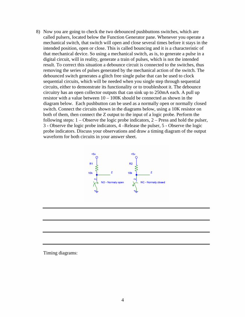
8) Now you are going to check the two debounced pushbuttons switches, which are called pulsers, located below the Function Generator pane. Whenever you operate a mechanical switch, that switch will open and close several times before it stays in the intended position, open or close. This is called bouncing and it is a characteristic of that mechanical device. So using a mechanical switch, as is, to generate a pulse in a digital circuit, will in reality, generate a train of pulses, which is not the intended result. To correct this situation a debounce circuit is connected to the switches, thus removing the series of pulses generated by the mechanical action of the switch. The debounced switch generates a glitch free single pulse that can be used to clock sequential circuits, which will be needed when you single step through sequential circuits, either to demonstrate its functionality or to troubleshoot it. The debounce circuitry has an open collector outputs that can sink up to 250mA each. A pull up resistor with a value between 10 – 100K should be connected as shown in the diagram below. Each pushbutton can be used as a normally open or normally closed switch. Connect the circuits shown in the diagrams below, using a 10K resistor on both of them, then connect the Z output to the input of a logic probe. Perform the following steps: 1 – Observe the logic probe indicators, 2 – Press and hold the pulser, 3 - Observe the logic probe indicators, 4 –Release the pulser, 5 - Observe the logic probe indicators. Discuss your observations and draw a timing diagram of the output waveform for both circuits in your answer sheet.
Timing diagrams:
5
9) The trainer kit provides you with two BCD seven segment LED displays. They are located below the logic probe pane. The BCD encoded information should be connected to the input terminals labeled D, C, B, and A, D being the most significant bit. Connect these terminals to 8 logic switches. Now, using the logic switches, output the BCD values from 0 to 9 and verify that the seven segment displays are working correctly. Indicate in your answer sheet, if the seven segment displays are working correctly or not. Also, tell me what is displayed on the seven segment LED display when the binary values 10 through 15 are sent to it.
LED display No. 1: _______________ LED display No. 2: _______________
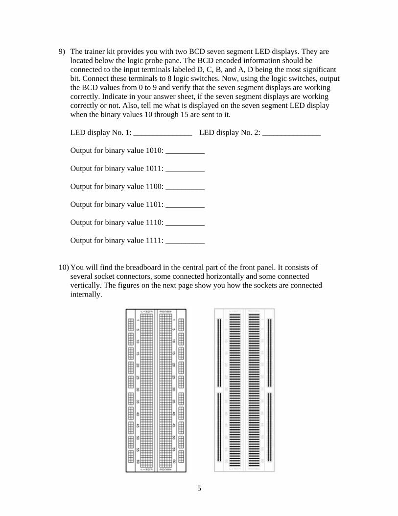
Output for binary value 1010: __________ Output for binary value 1011: __________ Output for binary value 1100: __________ Output for binary value 1101: __________ Output for binary value 1110: __________ Output for binary value 1111: __________ 10) You will find the breadboard in the central part of the front panel. It consists of
several socket connectors, some connected horizontally and some connected vertically. The figures on the next page show you how the sockets are connected internally.

6
11) Now you will wire and test an IC. Any time you are wiring a circuit or modifying it in any way, make sure the circuit is not energized. Turn the trainer’s power switch off. Get a 74LS08 (quad two input AND gates) IC, and connect the gate’s inputs to the logic switches, the outputs to the logic monitors, and the supply pins to the 5V power supply. You can obtain the correct pin diagram for the 74LS08 from the EE2731 website. Power the trainer up and then verify if all the gates in the 74LS08 are working properly. Practice how to use the chip extractor to remove the chip from the breadboard without bending or breaking their pins. Confirm your observations by using the chip tester to re-verify if the chip is working properly. First read all instructions given below then proceed to test the chip:
• Find the chip tester and turn it on.
• Wait for the tester to go through its initialization procedure.
• Set the socket’s lever vertical so that you may insert the chip on the socket.
• Insert the chip in the ZIF - zero insertion force socket at lower end of the tester, making sure the chip is aligned with the bottom end of the socket and that pin one of the chip is set towards the top end.
• Clamp the chip down by moving the lever to the horizontal position.
• Press the search button, and verify that the display correctly indicates the chip’s number, in your case 74:008.
• Press the test button, and a message indicating the if the chip is good or bad is shown.
Return all parts and tools to their proper places, and then clean your station.

7
Experiment 1 - Combinational Logic Circuits Combinational logic circuits are defined as circuits whose outputs depend only on the present value of their inputs.
Design Procedure
1 – From the problem statement find the number of input variables and the number of required output variables. Assign them meaningful names.
2 – Create a truth table that defines a relationship between input and output.
3 – Obtain a simplified Boolean function for each output.
4 – Draw the logic diagram.
Experiment:
1a. Design and build a combinational logic circuit with four inputs and four outputs that multiplies two 2-bits numbers, labeled X1 , X0 , and Y1 , Y0 . The outputs are labeled Z3, Z2 , Z1 , and Z0. Use AND, OR and NOT gates.
1b. Repeat “1a” and this time design the circuit using NAND gates only. Use the least number of gates you possibly can.

8
Experiment 2 - Boolean function realization using decoders and multiplexers
Function Realization with Decoders
A binary decoder converts a n-bits binary number into a 1-of-m code where m = 2n. This means that a single output has a different logic value from all other and that output identifies the 2n minterm of the n bits present at the input. Considering that any Boolean function may be expressed as a sum of minterms, one may add, with some OR gates, the outputs of the decoder that represents the required minterms thus forming the desired Boolean function.
Function Realization with Multiplexers
A multiplexer is basically a n-bit binary decoder with an extra input line added to each product term, and whose outputs are ORed together. Each product term may be enabled or disabled, by setting their respective extra input line to either logic 1 or logic 0 , thus generating the desired sum of minterms. One may improve on the previous procedure by using the following artifice:
- assume n = m +1;
- use a 2m to 1 multiplexer and connect m input variables to the m select lines;
- the remaining input variable, which for simplicity is labeled as A, is used to excite the data inputs of the multiplexer. Now these inputs can be excited with the following values: A, A’, 1 or 0, thus generating the desired sum of minterms.
Experiment:
A full adder circuit computes the sum of three one bit inputs, A, B, and CARRY_IN, and it generates two outputs, SUM and CARRY_OUT.
1a. Design and build a full adder using NAND(74LS00-2 inputs, 74LS10-3 inputs, 74LS20-4 inputs) gates only.
1b. Design and build a full adder using two 8 to 1 multiplexers.
1c. Design and build a full adder using two 4 to 1 multiplexers and a single inverter.
1d. Design and build a full adder using a single 3 to 8 decoder and some NAND gates.

9
Experiment 3 - Flip-flops Sequential logic circuits are defined as circuits whose outputs depends both on the present values of the inputs and the present state of the circuit. Latches and flip-flops are basic sequential circuit whose operation you will investigate with this experiment. The difference between these two sequential devices is that a flip-flop’s outputs change only at specific times determined by a clocking signal, while a latch’s outputs change independent of a clocking signal. Experiments: 1 – Construct a SR latch with an enable with a single 74LS00, and connect its three inputs S’, R’ and C to three switches and its two outputs Q and Q’ to two logic monitors so that you may verify its operation.
- Obtain a truth table of the circuit. - Set both the S’ and R’ inputs of the latch to logic 0 and the C input to logic 1.
Change the C input to logic 0 while observing the outputs. Discuss your findings.
2 – Construct a D latch by modifying the SR latch you built in experiment 1. This latch should have two inputs, D and C (enable), and two outputs Q and Q’. Connect D and C to two switches and Q and Q’ to two logic monitors, so you may verify its operation.
- Obtain a truth table of the circuit. - Discuss the differences between this latch and the SR latch.
3 – Construct a master-slave JK flip-flop with two 74LS00 and one 74LS10. Connect the J and K inputs to switches and the CLK input to a pulser. Now connect the outputs of the master latch to two logic monitors and the outputs of the slave latch to another two logic monitors, so you may observe the latch’s operation.
- Set both the J and K inputs to one then press and hold the pulser always observing the outputs. Release the pulser and again observe the outputs. Repeat the procedure a few times then discuss the transfer sequence from the input to the output of the master, then from the output of the master to the output of the slave.
- Verify the flip-flop’s operation and obtain a truth table for it. - Discuss the differences between the D latch and the JK flip-flop, specially,
with regards to when the outputs of these devices are allowed to change.
Include your observations in the lab report.

10
Experiment 4 - Counters A counter is a sequential circuit which goes through a sequence of states upon the application of input pulses. Its state diagram contains a single cycle. Counters may be classified as synchronous or asynchronous (ripple counter), and by its modulus, which is the number of states in its cycle.
Sequential Logic Circuit Design Procedure
1 – From the information given in the problem statement create a state diagram, then a state output table. You may start directly with the state output table, by eliminating the state diagram step, but I caution you that with some problems it is easier to visualize the sequential states sequence through the use of a state diagram.
2 – Minimize the number of states in the state output table by eliminating equivalent states. Two states are equivalent if they produce the same output and their next states are the same.
3 – Derive a transition output table by substituting each state from the state output table with a set of state variables whose values uniquely identify each state.
4 – Determine the type of flip-flop to be used in the design, then construct their excitation table. These table show which input values are needed by the flip-flop to reach the desired next state for each state input combination.
6 – Derive the flip-flop’s input excitation function, from the excitation table.
7 – Derive the output equation(s) from the transition output table.
8 – Draw the logic diagram. Experiments:
A - Design and build a synchronous decade counter with an enable. This counter should count from 0 to 9, and then repeat. Test if the counter is self starting by initializing the counter using the preset and clear inputs, to each of the six invalid states, 11 through 15. The application of input pulses should transfer the counter to a valid state in the case the counter is self starting. Discuss your findings in the report.
B – Cascade the counter designed in part A with another decade counter, 74LS90, to create a 0 to 99 counter. This is done by connecting the MSB of the output of the counter designed by you to input A of the 74LS90. Connect the output of the counter to the on-board 7-segment LED display, and its input to the TTL output of the function generator.

11
Experiment 5 - Shift Registers
In its simplest form a shift register is a register capable of shifting its data content either to the right or the left.
Experiment:
A – Design and build a 4-bit shift register with four D flip-flops and four 4-1 multiplexers. This circuit should be capable of performing the following functions:
Mode Control:
RESET’ S1 S0 Register Operation
0 X X Clear output
1 0 0 Complement
1 0 1 Rotate Right
1 1 0 Shift Left
1 1 1 Parallel Load
Inputs: Serial: SLI – Shift left input. Connect to logic switches.
Parallel: I3(MSB), I2, I1, and I0 – 4 bit parallel input. Connect to logic switches.
Reset: RESET. Connect to logic switches.
Clock: CLK – Use a pulser or the function generator TTL output to simulate a
clock input.
Outputs: O3 (MSB), O2, O1, and O0 – outputs of the four flip-flops. Connect to LEDs.
Explanation of register operation:
Parallel Load: Loads the 4-bits input, I3 – I0, into register.
Rotate Right: Rotate the data to the right one position per clock pulse.
Shift Left: Shifts the data to the left one position per clock pulse, with input from SLI.
No change: Data is complemented. Reset’: Output is cleared to zero.

12
Experiment 6 - Sequence Detector In general, a sequence detector is a sequential logic circuit used to check an input stream of bits and detect a specific sequence.
Experiments:
A – Design a sequential logic circuit to check an input stream labeled X and to produce an output Z=1 for any input sequence ending in 101 and 1001. Use the following test sequence to verify your circuits operation:
X = 110100110010110
Z = 000100100010100
Make sure your circuit has a start state and the means to manually reset the flip-flops to the start state. Note that sequences may overlap, i.e., the circuit does not reset to the start state when an output Z=1 occurs. Testing your circuit will involve checking the correctness of every state and next states for all possible combination of inputs.
B - Design a sequential logic circuit to check an input stream labeled X and to produce an output Z=1 if the total number of zeros received is odd and the sequence 100 has occurred at least once. The total number of zeros received include before, during and after the sequence 100 is received. Make sure your circuit is a Moore circuit and it has a start state and the means to manually reset the flip-flops to the start state. Note that the circuit does not reset to the start state when an output Z=1 occurs. Testing your circuit will involve checking the correctness of every state and next states for all possible combination of inputs.
C - Design a sequential logic circuit to check an input stream labeled X and to produce an output Z=0 if the total number of ones received is even and the sequence 010 has occurred at least once. The total number of ones received include before, during and after the sequence 010 is received. Make sure your circuit has a start state and the means to manually reset the flip-flops to the start state. The circuit should use the Moore model, and it should not reset to the start state when an output Z=0 occurs. Testing your circuit will involve checking the correctness of every state and next states for all possible combination of inputs.

13
Experiment 7 - Arithmetic Logic Unit An arithmetic and logic unit is a combinational logic circuit capable of performing several arithmetic and logic functions, selected by a set of function-select inputs, on a pair of n-bit operands. Assume the data to be active high for this experiment.
Experiment:
A – Design and build an 8-bit A.L.U. and a combinational logic circuit (decoder) which will be used to select a subset of the possible operations performed by the A.L.U. The A.L.U. available for your use are 4-bits ones, therefore you will need to cascade them together. The combinational logic circuit used to select which operations to perform with the A.L.U. has three inputs labeled A, B, and C, and 6 outputs which will drive the A.L.U.’s select inputs (S3, S2, S1, S0, and M of both A.L.U. and Cn of the least significant A.L.U.). The table shown below lists the functions the decoder circuit will select out of the many possible ones provided by the 74LS181 A.L.U.
A B C Function 0 0 0 A’ (Complement A) 0 0 1 A⊕B (A exclusive-OR B) 0 1 0 A+B (A OR B) 0 1 1 AB (A AND B) 1 0 0 A 1 0 1 A + B (A PLUS B) 1 1 0 A – B (A MINUS B) 1 1 1 ZERO

14
Experiment 8 - Traffic Light Controller There are many applications for controller circuits. One of them is a highway intersection traffic light. In this experiment you will design and implement a 4-way traffic light controller that uses pressure activated sensors embedded into the roadway to determine the sequence of light changes used to optimize the flow of traffic.
System requirements:
The system has 4 input sensors, north (N), south (S), east (E) and west (W), and 6 output lights, N/S (red, yellow and green), and E/W (red, yellow and green). Four data switches are used to simulate the sensors embedded on the road, and six LEDs are used to simulate the lights. A counter will be used to determine the amount of time each lamp stays on/off, and a flip-flop is used to determine which direction the traffic is flowing, i.e. N/S red is the complement of E/W red. Details about the design:
1. The traffic light cycle is as follows, assuming traffic is flowing in both directions, i.e. the road sensors detect cars in both directions:
• Starting with N/S light being red, the counter should count 12 pulses to change the E/W green light to yellow, then count another 4 pulses before simultaneously turning the E/W light red and the N/S light green. The cycle repeats but this time the N/S light will be green during 12 pulses, then yellow for four pulses, and finally it will turn red simultaneously with the E/W light turning green, which brings the cycle back to the beginning.
2. Even though the information provided below may seem obvious, it is always better to have all facts stated explicitly:
• At any given instance both directions may not be red, i.e., assume one direction is red and the other green or yellow.
• When cars are detected flowing in only one direction, that direction should remain green.
• When cars are not detected in either direction, the lights should not change.
• If a car stops at a red light and makes a right turn, then the count should start and as soon as the car leaves it should stop.
• If any yellow light is ON, the count should continue even if there are no cars waiting.

15
• When cars are flowing in both directions the lights should toggle every 16 counts as described above.
• Since the 74LS93 doesn’t have a stop count feature, a gate should be used to turn the clock going to the counter on or off as needed.
16
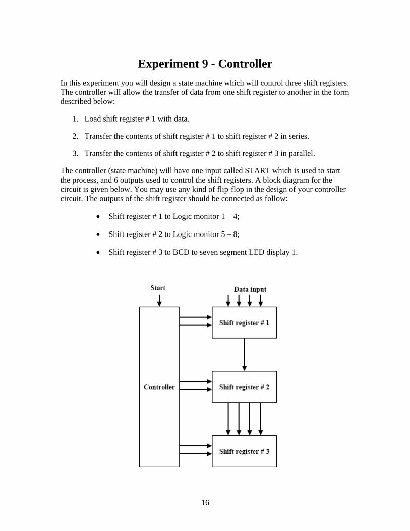
Experiment 9 - Controller In this experiment you will design a state machine which will control three shift registers. The controller will allow the transfer of data from one shift register to another in the form described below:
1. Load shift register # 1 with data.
2. Transfer the contents of shift register # 1 to shift register # 2 in series.
3. Transfer the contents of shift register # 2 to shift register # 3 in parallel.
The controller (state machine) will have one input called START which is used to start the process, and 6 outputs used to control the shift registers. A block diagram for the circuit is given below. You may use any kind of flip-flop in the design of your controller circuit. The outputs of the shift register should be connected as follow:
• Shift register # 1 to Logic monitor 1 – 4;
• Shift register # 2 to Logic monitor 5 – 8;
• Shift register # 3 to BCD to seven segment LED display 1.

17
Experiment 10 - Elevator Control There are many applications for controller circuits. One of them is an elevator control. In this experiment you are going to design a sequential logic circuit that may be used to control elevators.
Experiment A
System requirements:
The system has 2 inputs and 3 outputs:
Inputs
1 or Down – It represents a button located inside the elevator or on the first floor, which may be used to take the elevator to the first floor, from any floor.
2 or Up - It represents a button located inside the elevator or on the second floor, which may be used to take the elevator to the second floor, from any floor.
Outputs
1st floor – When this output is equal to logic 1, it indicates the elevator is at the 1st floor.
2nd floor – When this output is equal to logic 1, it indicates the elevator is at the 2nd floor.
Door - When this output is equal to logic 1, it indicates the elevator door is open. Details about the design:
2. The system has four states, 1st floor open door, 1st floor closed door, 2nd floor open door, and 2nd floor closed door.
3. The elevator should remain at rest until someone presses a button. The rest states are defined to be the states where the door is closed.
4. If someone presses the 1 or Down button, the elevator should go to the 1st floor, open the door (1st floor = 1, door = 1) and remain in this state for a small amount of time, then close the door (1st floor = 1, door = 0).
5. If someone presses the 2 or Up button, the elevator should go to the 2nd floor, open the door (2nd floor = 1, door = 1) and remain in this state for a small amount of time, then close the door (2nd floor = 1, door = 0).
6. Use a 74LS93 counter chip to time and trigger the door closure. 7. Follow the procedure discussed in class and generate: state/output table,
transition/output table, excitation table, equations, and logic diagram. Implement the circuit using flip-flops of your choice.
18
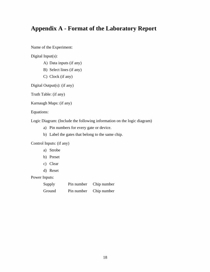
Appendix A - Format of the Laboratory Report
Name of the Experiment:
Digital Input(s):
A) Data inputs (if any)
B) Select lines (if any)
C) Clock (if any)
Digital Output(s): (if any)
Truth Table: (if any)
Karnaugh Maps: (if any)
Equations:
Logic Diagram: (Include the following information on the logic diagram)
a) Pin numbers for every gate or device.
b) Label the gates that belong to the same chip.
Control Inputs: (if any)
a) Strobe
b) Preset
c) Clear
d) Reset
Power Inputs:
Supply Pin number Chip number
Ground Pin number Chip number

19
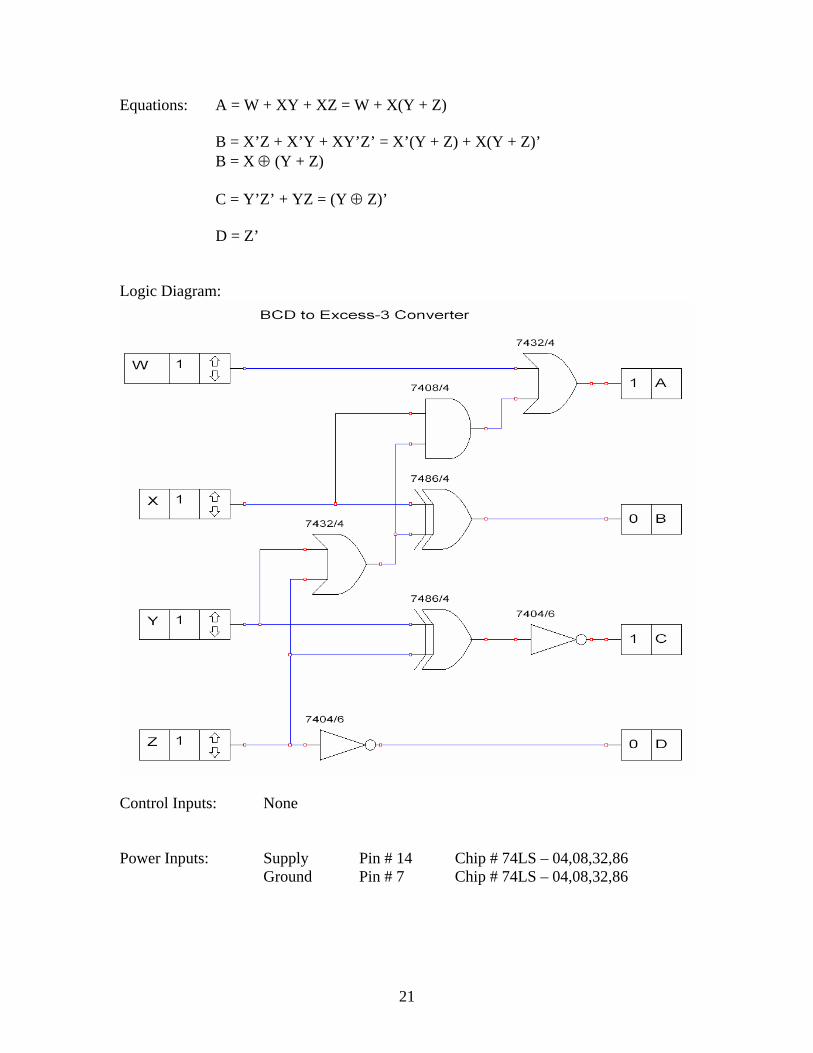
Appendix B - Example of a Laboratory Report BCD to Excess-3 Converter Design and build a combinational switching network that converts a binary coded decimal (BCD) digit into its Excess-3 code. Digital Inputs: Data Inputs: W, X, Y and Z from switches. Select Lines: None. Clock: None. Digital Output: A, B, C, and D Truth Table:
W X Y Z A B C D 0 0 0 0 0 0 1 1 0 0 0 1 0 1 0 0 0 0 1 0 0 1 0 1 0 0 1 1 0 1 1 0 0 1 0 0 0 1 1 1 0 1 0 1 1 0 0 0 0 1 1 0 1 0 0 1 0 1 1 1 1 0 1 0 1 0 0 0 1 0 1 1 1 0 0 1 1 1 0 0 1 0 1 0 X X X X 1 0 1 1 X X X X 1 1 0 0 X X X X 1 1 0 1 X X X X 1 1 1 0 X X X X 1 1 1 1 X X X X

20
Karnaugh Maps:
WX|YZ 00 01 11 10
00 0 0 0 0
01 0 1 1 1
11 X X X X
10 1 1 X X Map for A
WX|YZ 00 01 11 10
00 0 1 1 1
01 1 0 0 0
11 X X X X
10 0 1 X X Map for B
WX|YZ 00 01 11 10
00 1 0 1 0
01 1 0 1 0
11 X X X X
10 1 0 X X Map for C
WX|YZ 00 01 11 10
00 1 0 0 1
01 1 0 0 1
11 X X X X
10 1 0 X X Map for D
21
Equations: A = W + XY + XZ = W + X(Y + Z) B = X’Z + X’Y + XY’Z’ = X’(Y + Z) + X(Y + Z)’ B = X ⊕ (Y + Z) C = Y’Z’ + YZ = (Y ⊕ Z)’ D = Z’ Logic Diagram:
Control Inputs: None Power Inputs: Supply Pin # 14 Chip # 74LS – 04,08,32,86 Ground Pin # 7 Chip # 74LS – 04,08,32,86
22
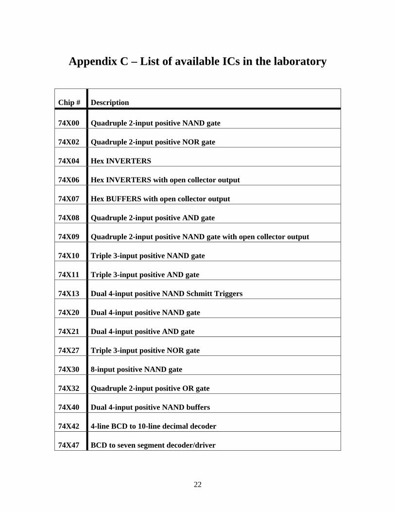
Appendix C – List of available ICs in the laboratory
Chip # Description
74X00 Quadruple 2-input positive NAND gate
74X02 Quadruple 2-input positive NOR gate
74X04 Hex INVERTERS
74X06 Hex INVERTERS with open collector output
74X07 Hex BUFFERS with open collector output
74X08 Quadruple 2-input positive AND gate
74X09 Quadruple 2-input positive NAND gate with open collector output
74X10 Triple 3-input positive NAND gate
74X11 Triple 3-input positive AND gate
74X13 Dual 4-input positive NAND Schmitt Triggers
74X20 Dual 4-input positive NAND gate
74X21 Dual 4-input positive AND gate
74X27 Triple 3-input positive NOR gate
74X30 8-input positive NAND gate
74X32 Quadruple 2-input positive OR gate
74X40 Dual 4-input positive NAND buffers
74X42 4-line BCD to 10-line decimal decoder
74X47 BCD to seven segment decoder/driver

23
Chip # Description
74X48 BCD to seven segment decoder/driver
74X51 AND-OR-INVERT gates
74X54 4-wide AND-OR-INVERT gates
74X70 AND-gated J-K positive edge triggered flip-flop with preset and clear
74X73 Dual J-K flip-flop with clear
74X74 Dual D-type positive edge triggered flip-flop with preset and clear
74X75 4-bit bi-stable latches
74X76 Dual J-K flip-flop with preset and clear
74X83 4-bit binary full adders with fast carry
74X86 Quadruple 2-input positive XOR gate
74X90 Decade counter
74X91 8-bit shift register
74X92 Divide by twelve counter
74X93 Binary counter
74X95 4-bit parallel access shift register
74X97 Synchronous 6-bit binary rate multiplier
74X138 3 line to 8 line decoder/demultiplexer
74X139 Dual 2 line to 4 line decoders/Demultiplexers
74X151 Data selector/multiplexer
74X153 Dual 4 line to 1 line data selectors/multiplexers
74X154 4 line to 16 line decoder/demultiplexer

24
Chip # Description
74X155 Dual 2 line to 4 line decoders/Demultiplexers
74X157 Quadruple 2 line to 1 line data selectors/multiplexers
74X181 Arithmetic logic unit/function generator
74X191 Synchronous up/down counter with down/up mode control
74X193 Synchronous 4-bit up/down counter (dual clock with clear)
74X194 4-bit bidirectional universal shift register