Embed Size (px)
Citation preview
An Approved Continuing Education Provider
PDHOnline Course E500 (5 PDH)
Digital Logic Design:
Combinational Logic
Mark A. Strain, P.E.
2016
PDH Online | PDH Center
5272 Meadow Estates Drive
Fairfax, VA 22030-6658
Phone & Fax: 703-988-0088
www.PDHonline.org
www.PDHcenter.com
www.PDHcenter.com PDHonline Course E500 www.PDHonline.org
©2016 Mark A. Strain ii
Table of Contents
Introduction ........................................................................................................................................... 2
Binary Numbering System ................................................................................................................... 2 Decimal Notation .............................................................................................................................. 3 Binary Notation ................................................................................................................................ 3
Binary to Decimal ........................................................................................................................ 3 Decimal to Binary ........................................................................................................................ 4
Negative numbers in Binary ............................................................................................................ 5
Ones’ Complement ....................................................................................................................... 5 Twos’ Complement ...................................................................................................................... 6
Hexadecimal Notation ...................................................................................................................... 7
Boolean Algebra ................................................................................................................................... 9 Basic Theorems ................................................................................................................................ 9 Commutative, Associative and Distributive Laws ......................................................................... 9
Commutative................................................................................................................................. 9 Associative .................................................................................................................................... 9 Distributive ................................................................................................................................... 9
Simplification Theorems ................................................................................................................ 10
DeMorgan's Theorem ..................................................................................................................... 10 Standard Forms of Boolean Expressions ...................................................................................... 11 Karnaugh Maps ............................................................................................................................... 12
Logic Operations and Logic Gates .................................................................................................... 16 Fundamental Logic Gates .............................................................................................................. 17
The AND Gate ............................................................................................................................ 17
The OR Gate ............................................................................................................................... 18 The NOT Gate ............................................................................................................................ 20
Combined Logic Gates ................................................................................................................... 21
The XOR Gate ............................................................................................................................ 22 The NAND Gate ......................................................................................................................... 22 The NOR Gate ............................................................................................................................ 23
The XNOR Gate ......................................................................................................................... 23 NAND Logic ................................................................................................................................... 24
Combinational Logic .......................................................................................................................... 27
Adder ............................................................................................................................................... 29 Half Adder .................................................................................................................................. 29 Full Adder ................................................................................................................................... 30
Ripple Carry Adders .................................................................................................................. 32 Decoder ........................................................................................................................................... 32
Binary Decoder ........................................................................................................................... 33
BCD to Seven-Segment Decoder .............................................................................................. 36 Encoder............................................................................................................................................ 37
Priority Encoder.......................................................................................................................... 38
Multiplexer ...................................................................................................................................... 39 Demultiplexer ................................................................................................................................. 42
Summary ............................................................................................................................................. 46

www.PDHcenter.com PDHonline Course E500 www.PDHonline.org
©2016 Mark A. Strain iii
References ........................................................................................................................................... 47
www.PDHcenter.com PDHonline Course E500 www.PDHonline.org
©2016 Mark A. Strain 2
Introduction You will encounter digital circuits multiple times in any given day. Digital circuits have
infiltrated society in ways unheard of only a few decades ago. They are everywhere and seem to
be in everything. Without them we would have no microprocessors. Without microprocessors we
would have no computers or smartphones or sophisticated fifth-generation fighter jets or even
something as simple and convenient as a coffee maker that brews the coffee before we wake up
that shuts off automatically when we forget to turn it off. Maybe we could still design a coffee
maker with an analog clock with a mechanical switch that will shut off the hot plate when the
clock advances forward past a mechanical set point, but the point is that these little devices (digital circuits) are commonplace and here to stay.
Digital circuits are comprised of tiny little on/off switches called transistors. The transistor is the
building block of all digital circuits. This revolutionary little switching device was invented in
1947 and its creators were awarded the Nobel Prize in Physics a few years later, and rightly so. Only a few other inventions have impacted and affected our lives in so many ways.
The transistor is the fundamental building block of digital circuits. It has been miniaturized by
many orders of magnitude since its inception. This has allowed for the explosive growth in the
complexity of digital circuits and microprocessors. Before the transistor computers were built
with mechanical switches called relays. There were bulky, slow and highly prone to failure. If
the computing industry was limited to using mechanical relays for processor cores, then the
progression in computing technology would have come to a halt decades ago. Simple "hand"
calculators would still be the size of a room and we would have no mobile phones not to mention a smartphone that understands the spoken language, "Siri, send a text".
Transistors can be organized into logic gates. The most basic gates are AND, OR and NOT. With
these fundamental gates, all other gates can be built. Boolean algebra describes logic gates in
symbolic form which gives a designer the ability to design a complicated logic circuit using math
by forming equations. These equations are directly transformed into logic symbols and into a
logic circuit. Connecting several logic gates together forms something called combinational
logic. With this combinational logic, adders can be fabricated as well as encoders, decoders,
multiplexers and demultiplexers. A multiplexer is a device that allows one input to be selected
from several inputs. An arithmetic logic unit (ALU) is a multiplexer which is at the heart of a microprocessor's core.
Binary Numbering System In everyday life we are used to the numbering system known as the decimal numeral system. Our
common numbering system is based on Arabic numerals (or symbols). Our numbering system is
also base-10 which means there are ten symbols (0, 1, 2, 3, 4, 5, 6, 7, 8 and 9) used to represent
every possible combination of numbers. Our numeral system is based on the number ten
probably because long ago we discovered that we each have ten fingers which are useful tools to
count on when doing simple math.
Computer systems and other digital systems use a numbering system based on a number other
than ten. Digital systems (such as a computer central processing unit) use a numbering system
www.PDHcenter.com PDHonline Course E500 www.PDHonline.org
©2016 Mark A. Strain 3
based on the number two. This base-2 numbering system is called the binary system. The binary system uses two symbols (0 and 1) to represent every possible combination of numbers.
Decimal Notation
When we write decimal (base-10) numbers, we use positional notation. This means that each
digit in a number is multiplied by a specific power of ten. The powers of ten (exponents) are
positive on the left side of the decimal point and the powers of ten (exponents) are negative on the right side of the decimal point.
For example, consider the decimal number 3854:
= 3(103) + 8(10
2) + 5(10
1) + 4(10
0)
= 3000 + 800 + 50 + 4
= 3854
Now consider the decimal number 1256.79:
= 1(103) + 2(10
2) + 5(10
1) + 6(10
0) + 7(10
-1) + 9(10
-2)
= 1000 + 200 + 50 + 6 + 0.7 + 0.09
= 1256.79
… 105 10
4 10
3 10
2 10
1 10
0 . 10
-1 10
-2 10
-3 10
-4 10
-5 …
1 2 5 6 . 7 9
Binary Notation
The binary system also uses positional notation. Each digit in the base-2 numbering system is
multiplied by a specific power of two. Just as in the base-10 system, the powers of two are
positive on the left side of the binary point and the powers of two are negative on the right side of the binary point.
Binary to Decimal
Each digit is a multiple of a power of 2. All digits to the left of the decimal point are positive powers of 2 and all digits to the right of the decimal point are negative powers of 2.
Consider the binary number 1011:
= 1(23) + 0(2
2) + 1(2
1) + 1(2
0)
= 8 + 0 + 2 + 1
= 11 (base-10)
Now consider the binary number 10101101.101:
= 1(27) + 0(2
6) + 1(2
5) + 0(2
4) + 1(2
3) + 1(2
2) + 0(2
1) + 1(2
0) + 1(2
-1) + 0(2
-2) + 1(2
-3)
= 128 + 0 + 32 + 0 + 8 + 4 + 0 + 1 + 1/2 + 0 + 1/8
= 173.625 (base-10)
… 28 2
7 2
6 2
5 2
4 2
3 2
2 2
1 2
0 . 2
-1 2
-2 2
-3 2
-4 2
-5 …
1 0 1 0 1 1 0 1 . 1 0 1
www.PDHcenter.com PDHonline Course E500 www.PDHonline.org
©2016 Mark A. Strain 4
Decimal to Binary
It is often necessary to represent a decimal fraction in binary. The integer part (to the left of the
decimal point) is converted to binary by continually dividing by 2 until you get to 1. The
fractional part is converted to binary by continually multiplying by 2 until you get 0 or a repeating sequence or you get tired.
Consider the decimal number 142.378:
First, convert the integer part:
Divide by 2 Remainder
142 / 2 0
71 / 2 1
35 / 2 1
17 / 2 1
8 / 2 0
4 / 2 0
2 / 2 0
1 1
Now, read the remainder part backwards and that is the binary representation of the integer part of the number: 10001110
Next, convert the fractional part. Start with the number to the right of the decimal point (0.378).
Multiply the number times 2 and record what is to the left of the decimal place after this
operation. Then take this number and discard whatever is to the left of the decimal place and continue.
0.378 * 2 = 0.756 → 0
0.756 * 2 = 1.512 → 1
0.512 * 2 = 1.024 → 1
0.024 * 2 = 0.048 → 0
0.048 * 2 = 0.096 → 0
0.096 * 2 = 0.192 → 0
0.192 * 2 = 0.384 → 0
0.384 * 2 = 0.768 → 0
0.768 * 2 = 1.536 → 1
0.536 * 2 = 1.072 → 1
0.072 * 2 = 0.144 → 0
0.144 * 2 = 0.288 → 0
0.288 * 2 = 0.576 → 0
0.576 * 2 = 1.152 → 1
0.152 * 2 = 0.304 → 0
…
Now, read the number forwards and that is the binary representation of the fractional part of the number: 0.011000001100010
www.PDHcenter.com PDHonline Course E500 www.PDHonline.org
©2016 Mark A. Strain 5
Therefore, 142.378 = 10001110.011000001100010…
Negative numbers in Binary
In mathematics, negative decimal numbers can be represented by using a minus “-“ sign. In
digital circuits numbers are represented only by a sequence of bits, either a 0 or a 1 and no plus
or minus sign. The most popular methods of representing signed numbers in binary are the ones'
complement and twos' complement methods. These methods allow subtraction to be performed
by adding the complement of a number instead of subtracting the number. The utilization of
ones' complement and twos' complement greatly simplifies digital circuits since addition is a
fundamental operation.
Ones’ Complement
The ones' complement of a binary number is obtained by negating the number by inverting all of
the bits. This is accomplished by changing all of the 0s into 1s and all of the 1s into 0s. The ones'
complement of a number behaves as the negative of the original number. An addition operation
is a fundamental operation in digital systems. There is no fundamental subtraction operation.
Subtraction of two numbers is equivalent to adding one number to the negative of the other
number. Therefore, any subtraction operation is equivalent to inverting one of the numbers and adding it to the other number.
Consider taking the ones' complement of the number 0000 1100 (base-2):
0000 1100
Invert all of the bits
1111 0011
Ones' complement is seldom used in digital systems because when a ones' complement number
is added to another number, the result is offset by –1. In other words, the result of a subtraction operation (using ones' complement) is off by –1.
Consider subtracting 8 from 12 using ones' complement:
ones' complement of 8:
0000 1000
Invert all of the bits
1111 0111
Now subtract 8 from 12:
12 – 8 = 4
Add the ones’ complement of 8 to 12: (12 – 8)
0000 1100
1111 0111
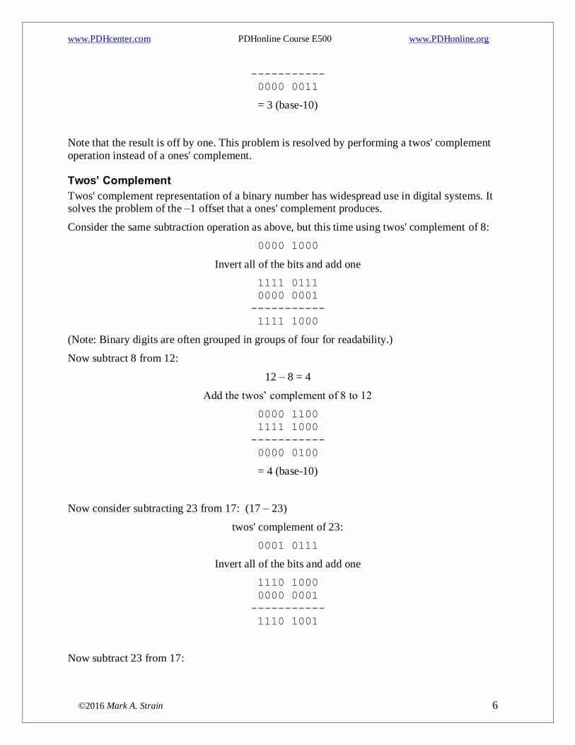
www.PDHcenter.com PDHonline Course E500 www.PDHonline.org
©2016 Mark A. Strain 6
-----------
0000 0011
= 3 (base-10)
Note that the result is off by one. This problem is resolved by performing a twos' complement
operation instead of a ones' complement.
Twos’ Complement
Twos' complement representation of a binary number has widespread use in digital systems. It solves the problem of the –1 offset that a ones' complement produces.
Consider the same subtraction operation as above, but this time using twos' complement of 8:
0000 1000
Invert all of the bits and add one
1111 0111
0000 0001
-----------
1111 1000
(Note: Binary digits are often grouped in groups of four for readability.)
Now subtract 8 from 12:
12 – 8 = 4
Add the twos’ complement of 8 to 12
0000 1100
1111 1000
-----------
0000 0100
= 4 (base-10)
Now consider subtracting 23 from 17: (17 – 23)
twos' complement of 23:
0001 0111
Invert all of the bits and add one
1110 1000
0000 0001
-----------
1110 1001
Now subtract 23 from 17:
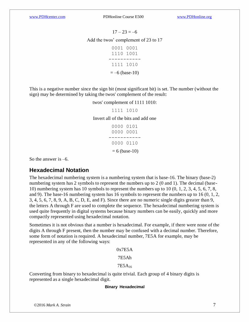
www.PDHcenter.com PDHonline Course E500 www.PDHonline.org
©2016 Mark A. Strain 7
17 – 23 = –6
Add the twos’ complement of 23 to 17
0001 0001
1110 1001
-----------
1111 1010
= –6 (base-10)
This is a negative number since the sign bit (most significant bit) is set. The number (without the sign) may be determined by taking the twos' complement of the result:
twos' complement of 1111 1010:
1111 1010
Invert all of the bits and add one
0000 0101
0000 0001
-----------
0000 0110
= 6 (base-10)
So the answer is –6.
Hexadecimal Notation
The hexadecimal numbering system is a numbering system that is base-16. The binary (base-2)
numbering system has 2 symbols to represent the numbers up to 2 (0 and 1). The decimal (base-
10) numbering system has 10 symbols to represent the numbers up to 10 (0, 1, 2, 3, 4, 5, 6, 7, 8,
and 9). The base-16 numbering system has 16 symbols to represent the numbers up to 16 (0, 1, 2,
3, 4, 5, 6, 7, 8, 9, A, B, C, D, E, and F). Since there are no numeric single digits greater than 9,
the letters A through F are used to complete the sequence. The hexadecimal numbering system is
used quite frequently in digital systems because binary numbers can be easily, quickly and more compactly represented using hexadecimal notation.
Sometimes it is not obvious that a number is hexadecimal. For example, if there were none of the
digits A through F present, then the number may be confused with a decimal number. Therefore,
some form of notation is required. A hexadecimal number, 7E5A for example, may be represented in any of the following ways:
0x7E5A
7E5Ah
7E5A16
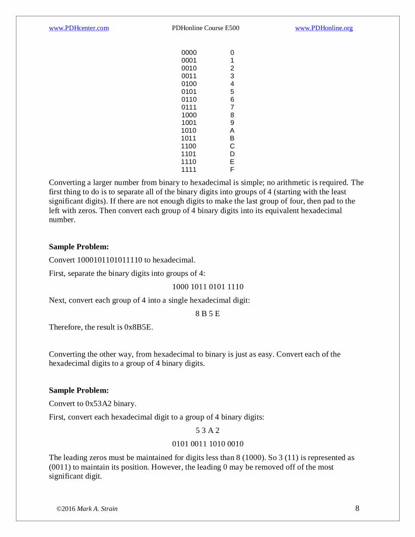
Converting from binary to hexadecimal is quite trivial. Each group of 4 binary digits is represented as a single hexadecimal digit.
Binary Hexadecimal
www.PDHcenter.com PDHonline Course E500 www.PDHonline.org
©2016 Mark A. Strain 8
0000 0 0001 1 0010 2 0011 3 0100 4 0101 5 0110 6 0111 7 1000 8 1001 9 1010 A 1011 B 1100 C 1101 D 1110 E 1111 F
Converting a larger number from binary to hexadecimal is simple; no arithmetic is required. The
first thing to do is to separate all of the binary digits into groups of 4 (starting with the least
significant digits). If there are not enough digits to make the last group of four, then pad to the
left with zeros. Then convert each group of 4 binary digits into its equivalent hexadecimal number.
Sample Problem:
Convert 1000101101011110 to hexadecimal.
First, separate the binary digits into groups of 4:
1000 1011 0101 1110
Next, convert each group of 4 into a single hexadecimal digit:
8 B 5 E
Therefore, the result is 0x8B5E.
Converting the other way, from hexadecimal to binary is just as easy. Convert each of the hexadecimal digits to a group of 4 binary digits.
Sample Problem:
Convert to 0x53A2 binary.
First, convert each hexadecimal digit to a group of 4 binary digits:
5 3 A 2
0101 0011 1010 0010
The leading zeros must be maintained for digits less than 8 (1000). So 3 (11) is represented as
(0011) to maintain its position. However, the leading 0 may be removed off of the most significant digit.
www.PDHcenter.com PDHonline Course E500 www.PDHonline.org
©2016 Mark A. Strain 9
Next, group the numbers together to get the answer:
101001110100010
It is acceptable to use either capital letters or lower case letters when representing the A–F digits
of a hexadecimal number, but consistency must be maintained within each number and the
within the context of a text, drawing or software code. In other words, be consistent; use either upper case or lower case, not both.
Large registers of numbers are usually represented using hexadecimal numbers instead of binary numbers for readability purposes.
Boolean Algebra Boolean algebra is essential to logic design. It is the basic mathematics needed for the study of
logic design in digital systems. The values of the variables are truth values (true and false)
denote as logic 1 and logic 0 respectively since the switching devices utilized in logic design are two-state devices (high or low).
Basic Theorems
A + 0 = A
A + 1 = 1
A • 1 = A A • 0 = 0
A + A = A
AA = A
(A')' = A
A + A' = 1 AA' = 0
Commutative, Associative and Distributive Laws
Commutative
AB = BA
A + B = B + A
Associative
(AB)C = A(BC) = ABC (A + B) + C = A + (B + C) = A + B + C
Distributive
A(B + C) = AB + AC
www.PDHcenter.com PDHonline Course E500 www.PDHonline.org
©2016 Mark A. Strain 10
A + BC = (A + B)(A + C)
Simplification Theorems
AB + AB' = A
A + AB = A (A + B')B = AB
(A + B)(A + B') = A
A(A + B) = A AB' + B = A + B
DeMorgan's Theorem
(A + B)' = A'B' (AB)' = A' + B'
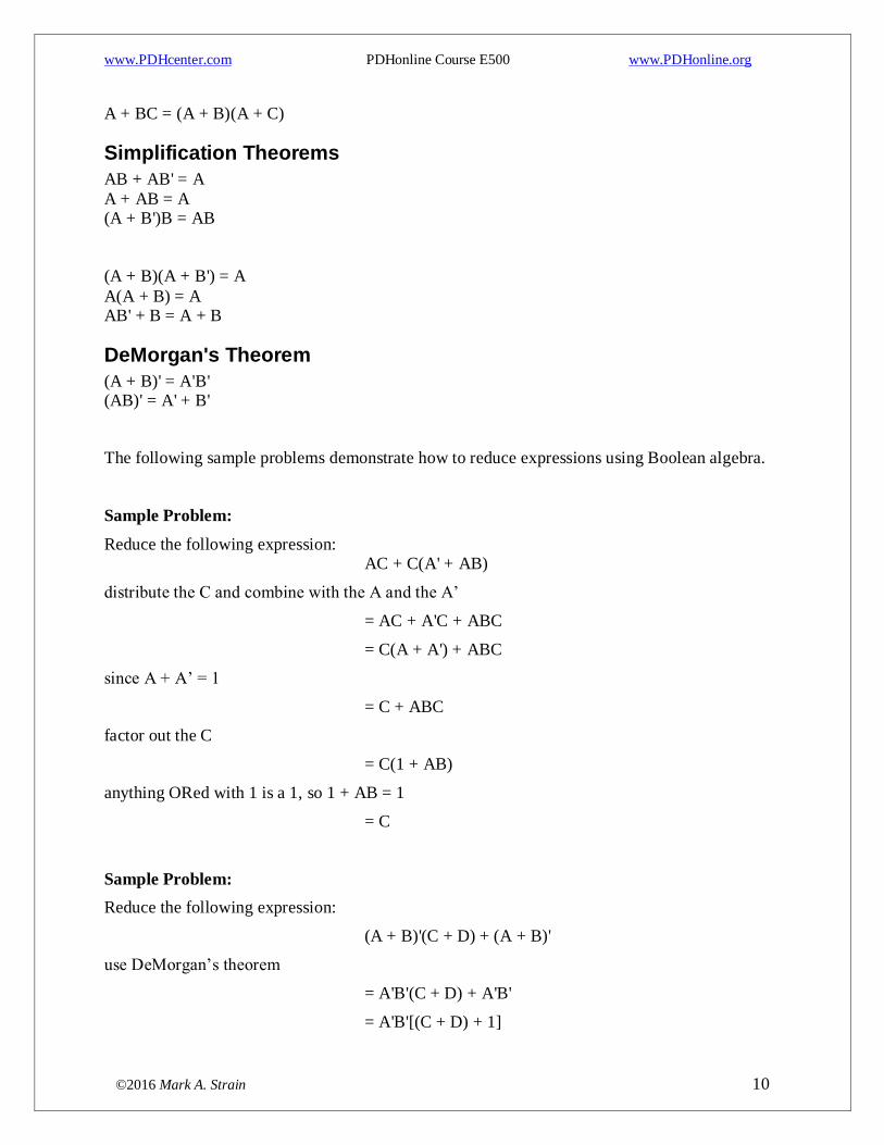
The following sample problems demonstrate how to reduce expressions using Boolean algebra.
Sample Problem:
Reduce the following expression: AC + C(A' + AB)
distribute the C and combine with the A and the A’
= AC + A'C + ABC
= C(A + A') + ABC
since A + A’ = 1
= C + ABC
factor out the C
= C(1 + AB)
anything ORed with 1 is a 1, so 1 + AB = 1
= C
Sample Problem:
Reduce the following expression:
(A + B)'(C + D) + (A + B)'
use DeMorgan’s theorem
= A'B'(C + D) + A'B'
= A'B'[(C + D) + 1]
www.PDHcenter.com PDHonline Course E500 www.PDHonline.org
©2016 Mark A. Strain 11
anything ORed with 1 is a 1, so (C + D) + 1 = 1
= A'B'
Sample Problem:
Reduce the following expression:
AB + ABCD
factor out the AB
= AB(1 + CD)
anything ORed with 1 is a 1, so 1 + CD = 1
= AB
Standard Forms of Boolean Expressions
There are two standard forms of Boolean expressions: the sum-of-products and the product-of-sums. Each form can be converted to the other.
A sum-of-products (SOP) expression is formed by summing two or more product terms. A
product term (also called a minterm) is a term like ABC. Summing product terms creates an
expression like
ABC + A’B + AC
A product-of-sums (POS) expression is formed by multiplying two or more sum terms. A sum
term is a term (also called a maxterm) like (A + B + C). Multiplying product terms creates an expression like
(A + B + C)(A’ + B)(A + C)
Converting from one form to another is achieved by taking the inverse twice of the whole
expression and then using DeMorgan’s Theorem. Taking the inverse twice gives the same result as the original expression, so the result of the equation is the same.
Sample Problem:
Convert a sum-of-products expression to a product-of-sums expression.
The following SOP expression
ABC + A’B + AC
is converted to a POS expression by inverting the expression twice:
((ABC + A’B + AC)’)’
Remember, in order to invert an expression like A + B, the terms must be inverted as well as the operator. So distribute the inverse function and the expression becomes
((ABC)’(A’B)’(AC)’)’ =
((A’ + B’ + C’)(A + B’)(A’ + C’))’
www.PDHcenter.com PDHonline Course E500 www.PDHonline.org
©2016 Mark A. Strain 12
Sample Problem:
Convert a product-of-sums expression to a sum-of-products expression.
The following POS expression
(A + B + C)(A’ + B)(A + C)
is converted to a SOP expression by inverting the expression twice:
[[(A + B + C)(A’ + B)(A + C)]’]’
Distribute the inverse function and the expression becomes
[(A + B + C)’ + (A’ + B)’ + (A + C)’]’ =
[A’B’C’ + AB’ + A’C’]’ =
[AB’ + B’A’C’ + A’C’]’ =
[AB’ + A’C’(B’ + 1)]’ =
[AB’ + A’C’]’ =
(A’ + B)(A + C) =
AA’ + A’C + AB + BC =
A’C + AB + BC
Another way to convert the POS expression (A + B + C)(A’ + B)(A + C) to a SOP expression is to distribute the terms:
(A + B + C)(A’ + B)(A + C) =
(A + B + C)(A’A + A’C + AB + BC) =
(A + B + C)(A’C + AB + BC) =
A’AC + AAB + ABC + A’BC + ABB + BBC + A’CC + ABC + ABC =
AB + ABC + A’BC + AB + BC + A’C + ABC + ABC =
AB + ABC + A’BC + AB + BC + A’C + ABC + ABC =
AB + ABC + A’BC + BC + A’C =
AB(1 + C) + A’C(B + 1) + BC =
AB + A’C + BC
Which is the same answer as above.
Karnaugh Maps
A Karnaugh map (also known as a K-map) is a method used to simply Boolean expressions.
Karnaugh maps are used to present the binary information in a way that allows easy grouping of
the terms that can be combined. A Karnaugh map is a representation of a truth table, reordered
into a grid. All of the position values in a Karnaugh map are either 0 or 1, just like in a truth
table. The cells of the grid are ordered in Gray code (00 01 11 10). Each cell position represents
www.PDHcenter.com PDHonline Course E500 www.PDHonline.org
©2016 Mark A. Strain 13
one combination of input conditions and each cell value represents the corresponding output
value. Optimal groups of 1s are identified and combined to form a minimal Boolean expression
representing the required logic.
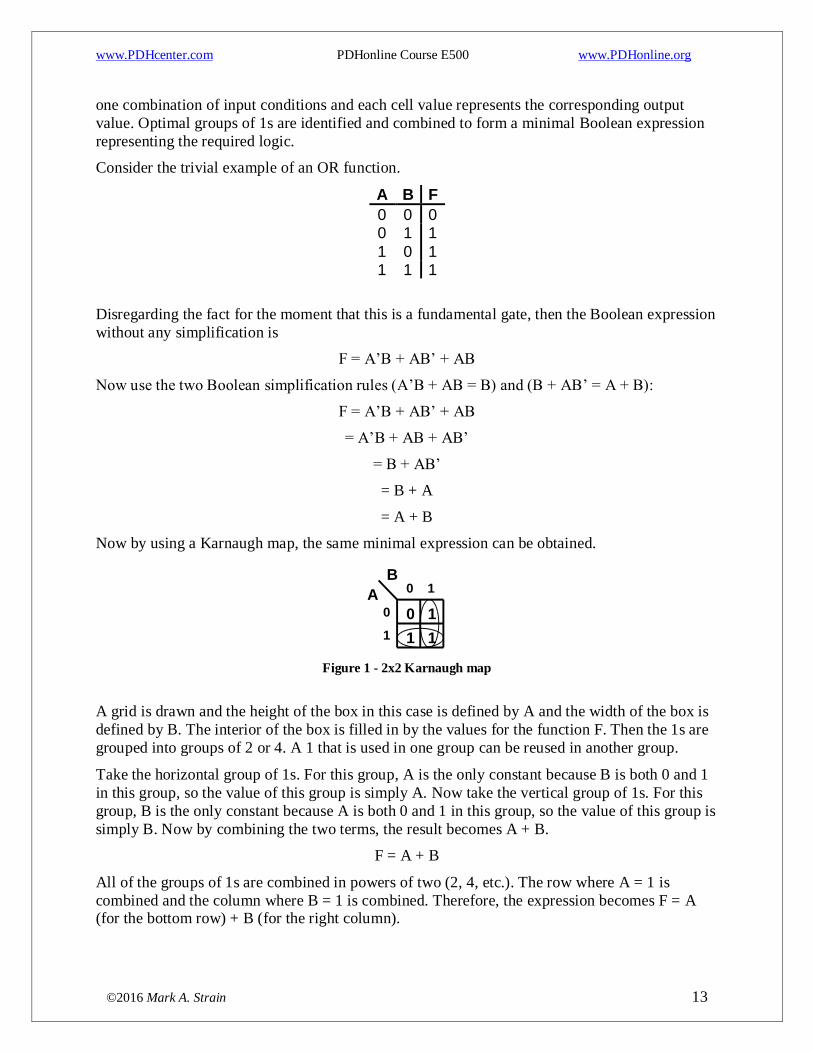
Consider the trivial example of an OR function.
A B F
0 0 0 0 1 1
1 0 1 1 1 1
Disregarding the fact for the moment that this is a fundamental gate, then the Boolean expression
without any simplification is
F = A’B + AB’ + AB
Now use the two Boolean simplification rules (A’B + AB = B) and (B + AB’ = A + B):
F = A’B + AB’ + AB
= A’B + AB + AB’
= B + AB’
= B + A
= A + B
Now by using a Karnaugh map, the same minimal expression can be obtained.
Figure 1 - 2x2 Karnaugh map
A grid is drawn and the height of the box in this case is defined by A and the width of the box is
defined by B. The interior of the box is filled in by the values for the function F. Then the 1s are
grouped into groups of 2 or 4. A 1 that is used in one group can be reused in another group.
Take the horizontal group of 1s. For this group, A is the only constant because B is both 0 and 1
in this group, so the value of this group is simply A. Now take the vertical group of 1s. For this
group, B is the only constant because A is both 0 and 1 in this group, so the value of this group is
simply B. Now by combining the two terms, the result becomes A + B.
F = A + B
All of the groups of 1s are combined in powers of two (2, 4, etc.). The row where A = 1 is
combined and the column where B = 1 is combined. Therefore, the expression becomes F = A (for the bottom row) + B (for the right column).
0 1
0 1
0
1
A
B
1 1
www.PDHcenter.com PDHonline Course E500 www.PDHonline.org
©2016 Mark A. Strain 14
Karnaugh maps are typically used to simplify more complex Boolean expressions, like truth tables that have three or four inputs variables.
When two adjacent cells both contain a 1, the two cells can be grouped and simplified
algebraically. Also in maps larger than a 2x2 grid, two adjacent pairs of cells all containing 1s
can be combined to form a group of four. This group of four can be simplified even further than
just having two cells. This process can continue in powers of two depending on the size of the
map. For example, two adjacent cells containing 1s forms a group of two. Four adjacent cells
(either 2x2 or 1x4 or 4x1) containing 1s forms a group of four. Eight adjacent cells (2x4 or 4x2) containing 1s forms a group of eight.
Sample Problem:
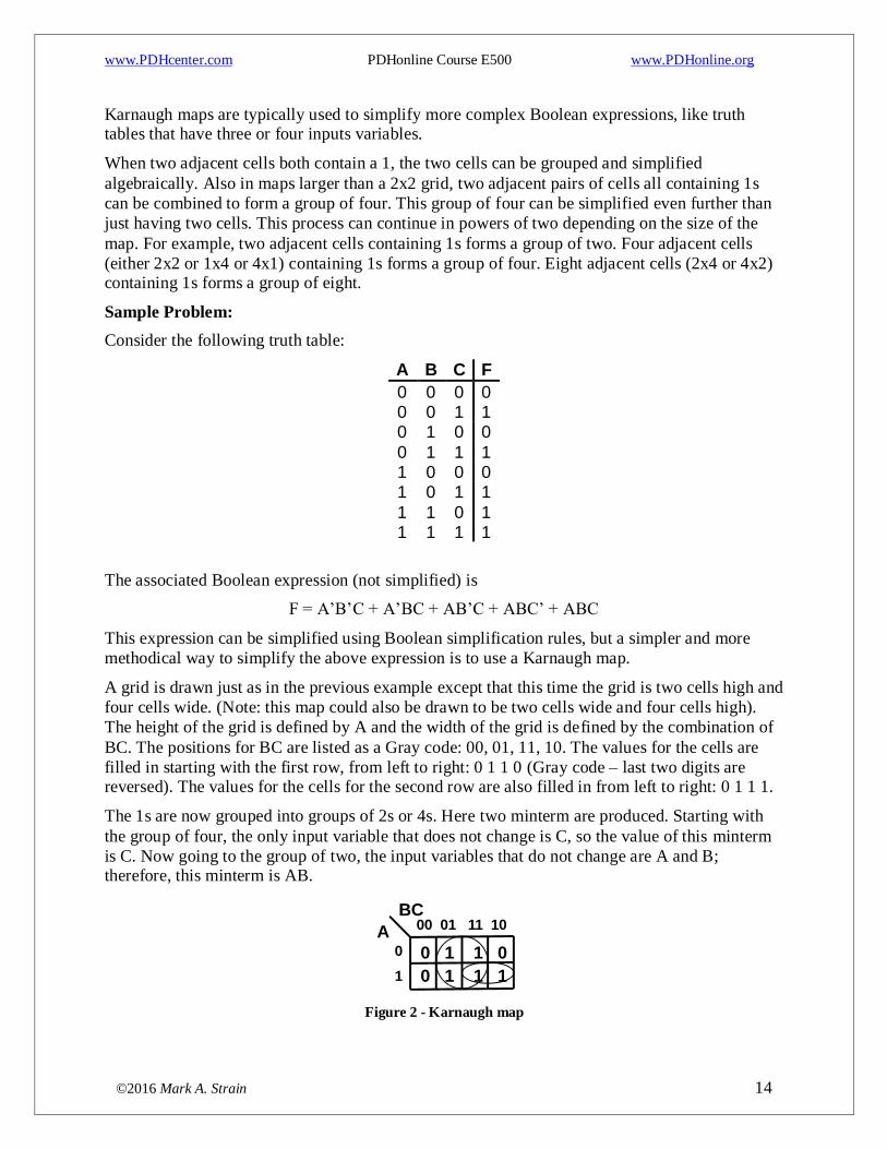
Consider the following truth table:
A B C F
0 0 0 0 0 0 1 1 0 1 0 0
0 1 1 1 1 0 0 0 1 0 1 1
1 1 0 1 1 1 1 1
The associated Boolean expression (not simplified) is
F = A’B’C + A’BC + AB’C + ABC’ + ABC
This expression can be simplified using Boolean simplification rules, but a simpler and more
methodical way to simplify the above expression is to use a Karnaugh map.
A grid is drawn just as in the previous example except that this time the grid is two cells high and
four cells wide. (Note: this map could also be drawn to be two cells wide and four cells high).
The height of the grid is defined by A and the width of the grid is defined by the combination of
BC. The positions for BC are listed as a Gray code: 00, 01, 11, 10. The values for the cells are
filled in starting with the first row, from left to right: 0 1 1 0 (Gray code – last two digits are reversed). The values for the cells for the second row are also filled in from left to right: 0 1 1 1.
The 1s are now grouped into groups of 2s or 4s. Here two minterm are produced. Starting with
the group of four, the only input variable that does not change is C, so the value of this minterm
is C. Now going to the group of two, the input variables that do not change are A and B; therefore, this minterm is AB.
Figure 2 - Karnaugh map
0 1 1 0
00 01 11 10
0
1
A
BC
0 1 1 1
www.PDHcenter.com PDHonline Course E500 www.PDHonline.org
©2016 Mark A. Strain 15
So, by combining the two minterms, the expression becomes AB + C. So the expression that started out as this
F = A’B’C + A’BC + AB’C + ABC’ + ABC
becomes this
F = AB + C
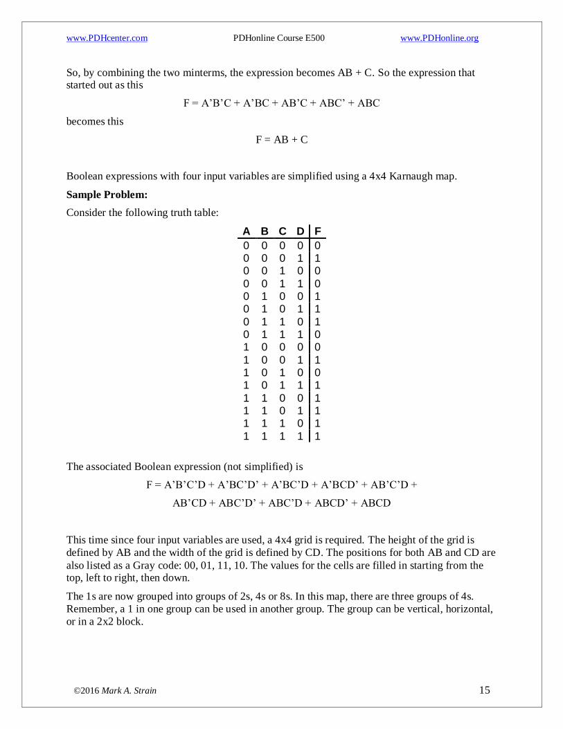
Boolean expressions with four input variables are simplified using a 4x4 Karnaugh map.
Sample Problem:
Consider the following truth table:
A B C D F
0 0 0 0 0 0 0 0 1 1 0 0 1 0 0
0 0 1 1 0 0 1 0 0 1 0 1 0 1 1
0 1 1 0 1 0 1 1 1 0 1 0 0 0 0
1 0 0 1 1 1 0 1 0 0 1 0 1 1 1
1 1 0 0 1 1 1 0 1 1 1 1 1 0 1
1 1 1 1 1
The associated Boolean expression (not simplified) is
F = A’B’C’D + A’BC’D’ + A’BC’D + A’BCD’ + AB’C’D +
AB’CD + ABC’D’ + ABC’D + ABCD’ + ABCD
This time since four input variables are used, a 4x4 grid is required. The height of the grid is
defined by AB and the width of the grid is defined by CD. The positions for both AB and CD are
also listed as a Gray code: 00, 01, 11, 10. The values for the cells are filled in starting from the top, left to right, then down.
The 1s are now grouped into groups of 2s, 4s or 8s. In this map, there are three groups of 4s.
Remember, a 1 in one group can be used in another group. The group can be vertical, horizontal,
or in a 2x2 block.
www.PDHcenter.com PDHonline Course E500 www.PDHonline.org
©2016 Mark A. Strain 16
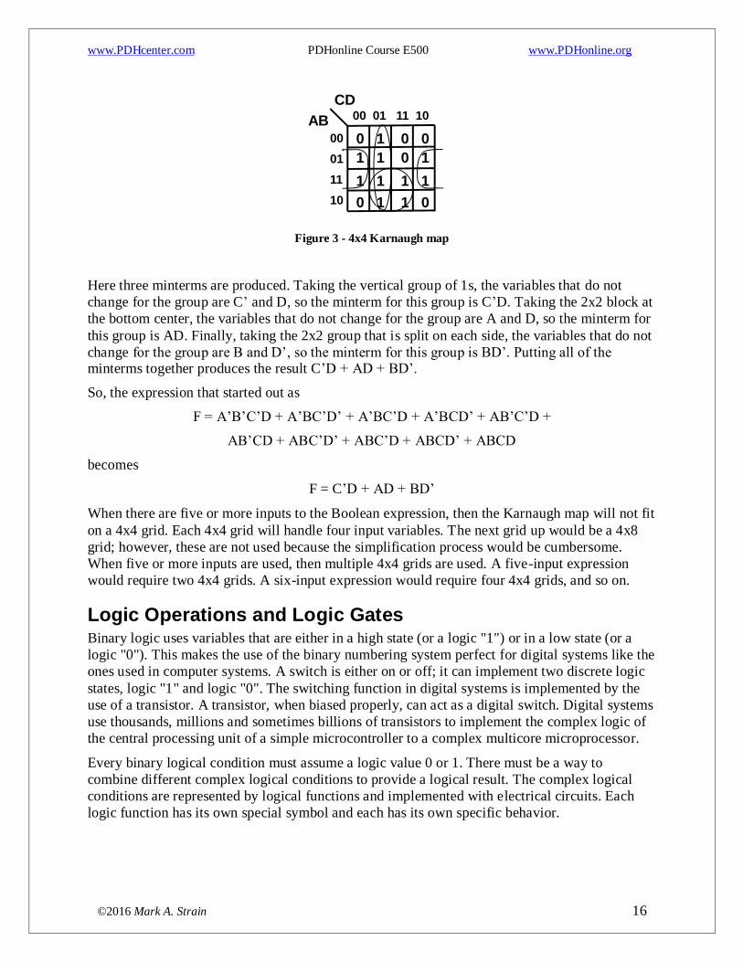
Figure 3 - 4x4 Karnaugh map
Here three minterms are produced. Taking the vertical group of 1s, the variables that do not
change for the group are C’ and D, so the minterm for this group is C’D. Taking the 2x2 block at
the bottom center, the variables that do not change for the group are A and D, so the minterm for
this group is AD. Finally, taking the 2x2 group that is split on each side, the variables that do not
change for the group are B and D’, so the minterm for this group is BD’. Putting all of the minterms together produces the result C’D + AD + BD’.
So, the expression that started out as
F = A’B’C’D + A’BC’D’ + A’BC’D + A’BCD’ + AB’C’D +
AB’CD + ABC’D’ + ABC’D + ABCD’ + ABCD
becomes
F = C’D + AD + BD’
When there are five or more inputs to the Boolean expression, then the Karnaugh map will not fit
on a 4x4 grid. Each 4x4 grid will handle four input variables. The next grid up would be a 4x8
grid; however, these are not used because the simplification process would be cumbersome.
When five or more inputs are used, then multiple 4x4 grids are used. A five-input expression
would require two 4x4 grids. A six-input expression would require four 4x4 grids, and so on.
Logic Operations and Logic Gates Binary logic uses variables that are either in a high state (or a logic "1") or in a low state (or a
logic "0"). This makes the use of the binary numbering system perfect for digital systems like the
ones used in computer systems. A switch is either on or off; it can implement two discrete logic
states, logic "1" and logic "0". The switching function in digital systems is implemented by the
use of a transistor. A transistor, when biased properly, can act as a digital switch. Digital systems
use thousands, millions and sometimes billions of transistors to implement the complex logic of
the central processing unit of a simple microcontroller to a complex multicore microprocessor.
Every binary logical condition must assume a logic value 0 or 1. There must be a way to
combine different complex logical conditions to provide a logical result. The complex logical
conditions are represented by logical functions and implemented with electrical circuits. Each
logic function has its own special symbol and each has its own specific behavior.
0 1 0 0
00 01 11 10
00
01
11
10
AB
CD
1 1 0 1
1 1 1 1
0 1 1 0
www.PDHcenter.com PDHonline Course E500 www.PDHonline.org
©2016 Mark A. Strain 17
The basic building blocks of a microcontroller or microprocessor are called logic gates. These
gates are basic electrical circuits that have at least one input and only one output. The input and
output values are logical values true (or 1) and false (or 0).
Gates have no memory; their output depends only on the value of the inputs. A gate's output is
sometimes called its logical function. The relationship of a logic gate's output versus its inputs is
best described by a truth table. A truth table lists every possible combination of inputs (in order)
in tabular form and presents the corresponding output value in a separate column.
The following is an example of a truth table with two inputs (A and B) and one output (F). The table lists every possible combination of inputs in order and each associated output.
A B F
0 0 0
0 1 0 1 0 0 1 1 1
Figure 4 - Truth Table
Fundamental Logic Gates
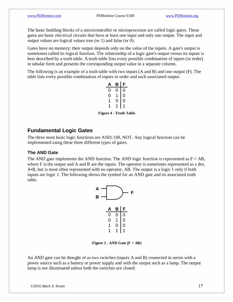
The three most basic logic functions are AND, OR, NOT. Any logical function can be implemented using these three different types of gates.
The AND Gate
The AND gate implements the AND function. The AND logic function is represented as F = AB,
where F is the output and A and B are the inputs. The operator is sometimes represented as a dot,
A•B, but is most often represented with no operator, AB. The output is a logic 1 only if both
inputs are logic 1. The following shows the symbol for an AND gate and its associated truth
table.
A B F
0 0 0
0 1 0 1 0 0 1 1 1
Figure 5 - AND Gate (F = AB)
An AND gate can be thought of as two switches (inputs A and B) connected in series with a
power source such as a battery or power supply and with the output such as a lamp. The output lamp is not illuminated unless both the switches are closed.
FA
B
www.PDHcenter.com PDHonline Course E500 www.PDHonline.org
©2016 Mark A. Strain 18
Figure 6 - AND gate composed of switches
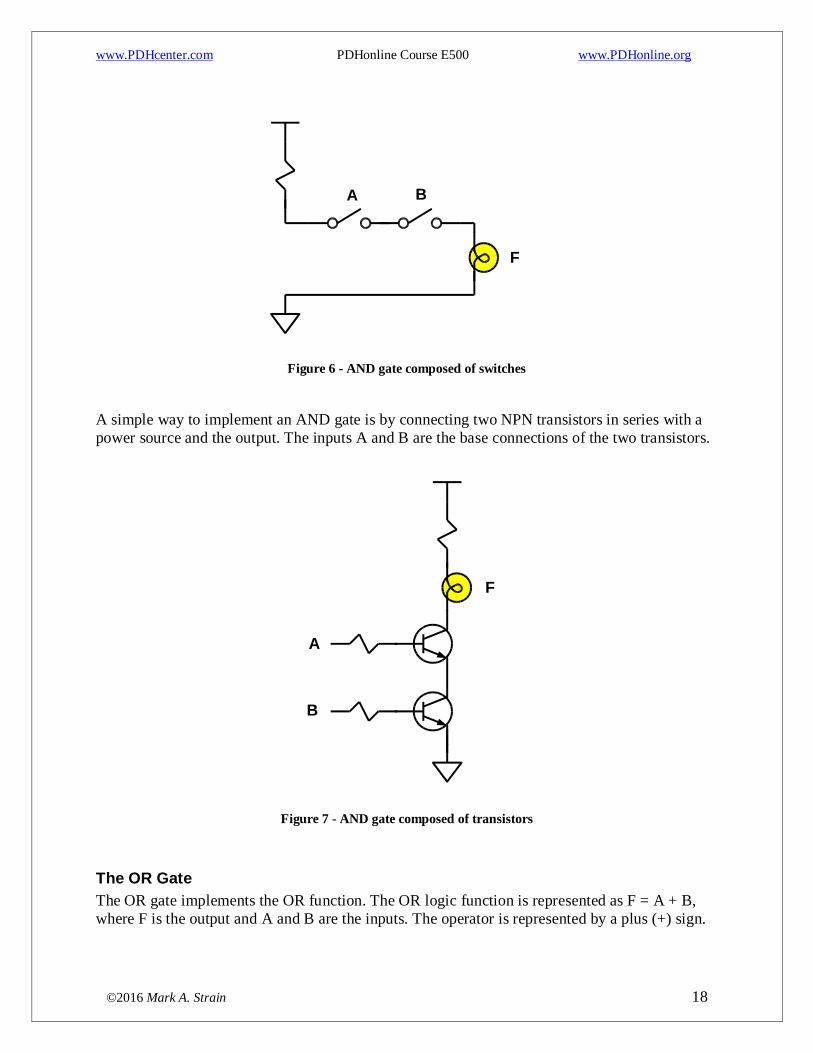
A simple way to implement an AND gate is by connecting two NPN transistors in series with a
power source and the output. The inputs A and B are the base connections of the two transistors.
Figure 7 - AND gate composed of transistors
The OR Gate
The OR gate implements the OR function. The OR logic function is represented as F = A + B,
where F is the output and A and B are the inputs. The operator is represented by a plus (+) sign.
F
A B
F
A
B
www.PDHcenter.com PDHonline Course E500 www.PDHonline.org
©2016 Mark A. Strain 19
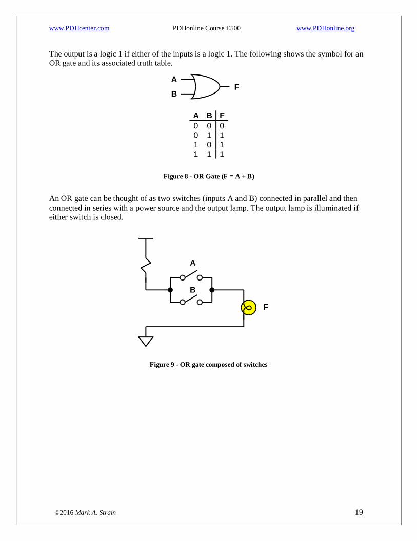
The output is a logic 1 if either of the inputs is a logic 1. The following shows the symbol for an OR gate and its associated truth table.
A B F
0 0 0 0 1 1
1 0 1 1 1 1
Figure 8 - OR Gate (F = A + B)
An OR gate can be thought of as two switches (inputs A and B) connected in parallel and then
connected in series with a power source and the output lamp. The output lamp is illuminated if either switch is closed.
Figure 9 - OR gate composed of switches
FA
B
F
A
B
www.PDHcenter.com PDHonline Course E500 www.PDHonline.org
©2016 Mark A. Strain 20
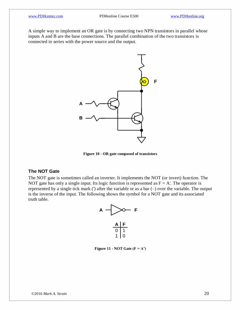
A simple way to implement an OR gate is by connecting two NPN transistors in parallel whose
inputs A and B are the base connections. The parallel combination of the two transistors is
connected in series with the power source and the output.
Figure 10 - OR gate composed of transistors
The NOT Gate
The NOT gate is sometimes called an inverter. It implements the NOT (or invert) function. The
NOT gate has only a single input. Its logic function is represented as F = A'. The operator is
represented by a single tick mark (') after the variable or as a bar (–) over the variable. The output
is the inverse of the input. The following shows the symbol for a NOT gate and its associated truth table.
A F
0 1 1 0
Figure 11 - NOT Gate (F = A’)
F
A
B
FA
www.PDHcenter.com PDHonline Course E500 www.PDHonline.org
©2016 Mark A. Strain 21
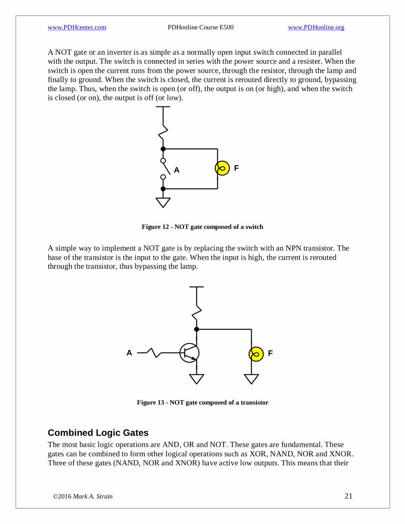
A NOT gate or an inverter is as simple as a normally open input switch connected in parallel
with the output. The switch is connected in series with the power source and a resister. When the
switch is open the current runs from the power source, through the resistor, through the lamp and
finally to ground. When the switch is closed, the current is rerouted directly to ground, bypassing
the lamp. Thus, when the switch is open (or off), the output is on (or high), and when the switch
is closed (or on), the output is off (or low).
Figure 12 - NOT gate composed of a switch
A simple way to implement a NOT gate is by replacing the switch with an NPN transistor. The
base of the transistor is the input to the gate. When the input is high, the current is rerouted through the transistor, thus bypassing the lamp.
Figure 13 - NOT gate composed of a transistor
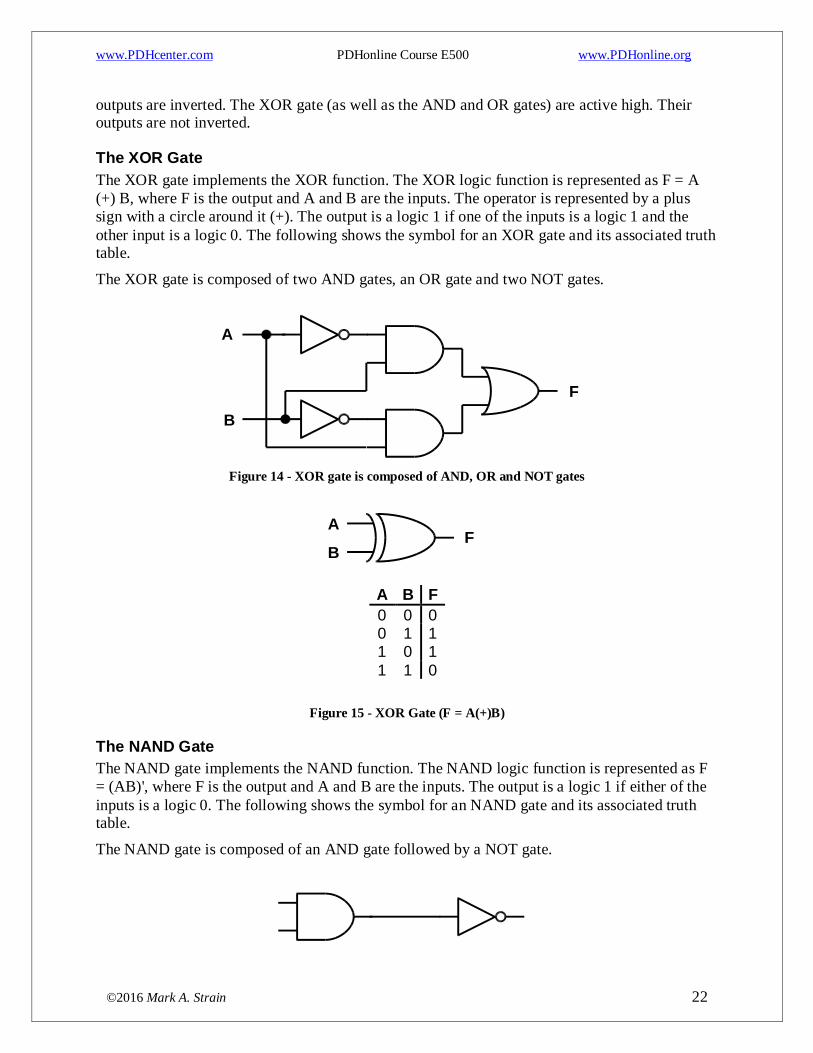
Combined Logic Gates
The most basic logic operations are AND, OR and NOT. These gates are fundamental. These
gates can be combined to form other logical operations such as XOR, NAND, NOR and XNOR.
Three of these gates (NAND, NOR and XNOR) have active low outputs. This means that their
FA
FA
www.PDHcenter.com PDHonline Course E500 www.PDHonline.org
©2016 Mark A. Strain 22
outputs are inverted. The XOR gate (as well as the AND and OR gates) are active high. Their outputs are not inverted.
The XOR Gate
The XOR gate implements the XOR function. The XOR logic function is represented as F = A
(+) B, where F is the output and A and B are the inputs. The operator is represented by a plus
sign with a circle around it (+). The output is a logic 1 if one of the inputs is a logic 1 and the
other input is a logic 0. The following shows the symbol for an XOR gate and its associated truth table.
The XOR gate is composed of two AND gates, an OR gate and two NOT gates.
Figure 14 - XOR gate is composed of AND, OR and NOT gates
A B F
0 0 0 0 1 1 1 0 1
1 1 0
Figure 15 - XOR Gate (F = A(+)B)
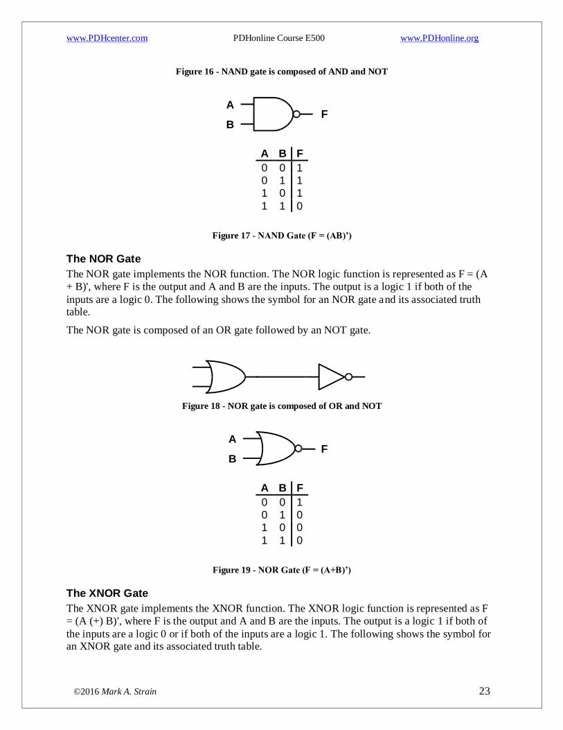
The NAND Gate
The NAND gate implements the NAND function. The NAND logic function is represented as F
= (AB)', where F is the output and A and B are the inputs. The output is a logic 1 if either of the
inputs is a logic 0. The following shows the symbol for an NAND gate and its associated truth table.
The NAND gate is composed of an AND gate followed by a NOT gate.
A
B
F
FA
B
www.PDHcenter.com PDHonline Course E500 www.PDHonline.org
©2016 Mark A. Strain 23
Figure 16 - NAND gate is composed of AND and NOT
A B F
0 0 1 0 1 1 1 0 1
1 1 0
Figure 17 - NAND Gate (F = (AB)’)
The NOR Gate
The NOR gate implements the NOR function. The NOR logic function is represented as F = (A
+ B)', where F is the output and A and B are the inputs. The output is a logic 1 if both of the
inputs are a logic 0. The following shows the symbol for an NOR gate and its associated truth table.
The NOR gate is composed of an OR gate followed by an NOT gate.
Figure 18 - NOR gate is composed of OR and NOT
A B F
0 0 1 0 1 0 1 0 0
1 1 0
Figure 19 - NOR Gate (F = (A+B)’)
The XNOR Gate
The XNOR gate implements the XNOR function. The XNOR logic function is represented as F
= (A (+) B)', where F is the output and A and B are the inputs. The output is a logic 1 if both of
the inputs are a logic 0 or if both of the inputs are a logic 1. The following shows the symbol for an XNOR gate and its associated truth table.
FA
B
FA
B
www.PDHcenter.com PDHonline Course E500 www.PDHonline.org
©2016 Mark A. Strain 24
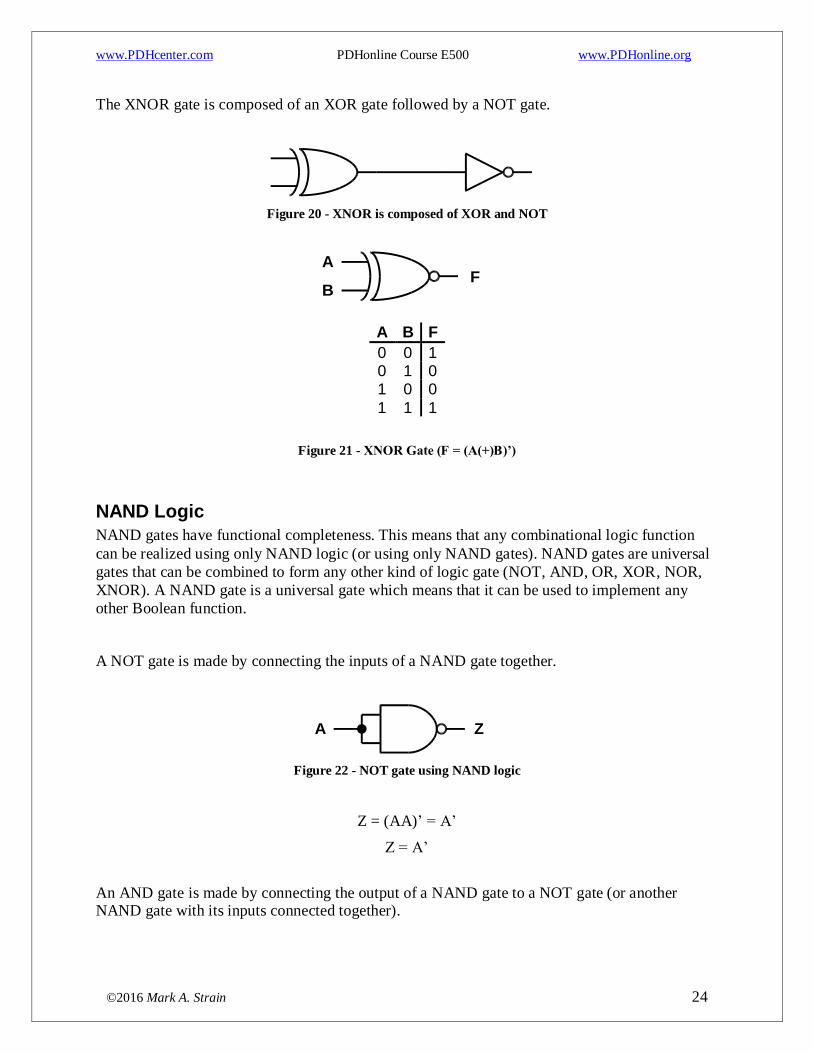
The XNOR gate is composed of an XOR gate followed by a NOT gate.
Figure 20 - XNOR is composed of XOR and NOT
A B F
0 0 1 0 1 0 1 0 0
1 1 1
Figure 21 - XNOR Gate (F = (A(+)B)’)
NAND Logic
NAND gates have functional completeness. This means that any combinational logic function
can be realized using only NAND logic (or using only NAND gates). NAND gates are universal
gates that can be combined to form any other kind of logic gate (NOT, AND, OR, XOR, NOR,
XNOR). A NAND gate is a universal gate which means that it can be used to implement any
other Boolean function.
A NOT gate is made by connecting the inputs of a NAND gate together.
Figure 22 - NOT gate using NAND logic
Z = (AA)’ = A’
Z = A’
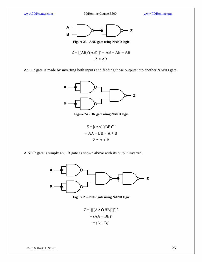
An AND gate is made by connecting the output of a NAND gate to a NOT gate (or another NAND gate with its inputs connected together).
FA
B
ZA
www.PDHcenter.com PDHonline Course E500 www.PDHonline.org
©2016 Mark A. Strain 25
Figure 23 - AND gate using NAND logic
Z = [(AB)’(AB)’]’ = AB + AB = AB
Z = AB
An OR gate is made by inverting both inputs and feeding those outputs into another NAND gate.
Figure 24 - OR gate using NAND logic
Z = [(AA)’(BB)’]’
= AA + BB = A + B
Z = A + B
A NOR gate is simply an OR gate as shown above with its output inverted.
Figure 25 - NOR gate using NAND logic
Z = {[(AA)’(BB)’]’}’
= (AA + BB)’
= (A + B)’
ZA
B
A
B
Z
A
B
Z
www.PDHcenter.com PDHonline Course E500 www.PDHonline.org
©2016 Mark A. Strain 26
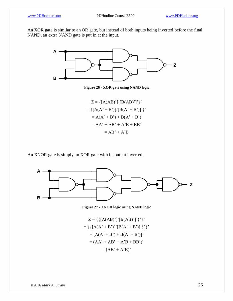
An XOR gate is similar to an OR gate, but instead of both inputs being inverted before the final NAND, an extra NAND gate is put in at the input.
Figure 26 - XOR gate using NAND logic
Z = {[A(AB)’]’[B(AB)’]’}’
= {[A(A’ + B’)]’[B(A’ + B’)]’}’
= A(A’ + B’) + B(A’ + B’)
= AA’ + AB’ + A’B + BB’
= AB’ + A’B
An XNOR gate is simply an XOR gate with its output inverted.
Figure 27 - XNOR logic using NAND logic
Z = {{[A(AB)’]’[B(AB)’]’}’}’
= {{[A(A’ + B’)]’[B(A’ + B’)]’}’}’
= [A(A’ + B’) + B(A’ + B’)]’
= (AA’ + AB’ + A’B + BB’)’
= (AB’ + A’B)’
A
B
Z
A
B
Z
www.PDHcenter.com PDHonline Course E500 www.PDHonline.org
©2016 Mark A. Strain 27
Combinational Logic Combinational logic uses a combination of gates to implement a desired result. Combinational
logic circuits are made up of basic logic gates that are "combined" together to produce a circuit
that has a specific purpose. With combinational logic an equation may be used to define a logic
function. Its output is a function only of its inputs. For example, in the equation Z = AB + C, the
output Z is derived only from its inputs. That means Z is a function of A, B and C, or Z = f(A, B, C).
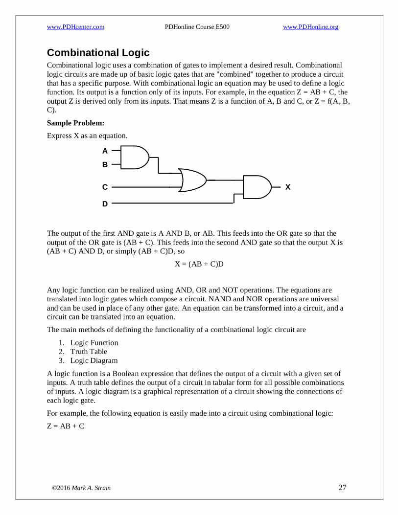
Sample Problem:
Express X as an equation.
The output of the first AND gate is A AND B, or AB. This feeds into the OR gate so that the
output of the OR gate is (AB + C). This feeds into the second AND gate so that the output X is (AB + C) AND D, or simply (AB + C)D, so
X = (AB + C)D
Any logic function can be realized using AND, OR and NOT operations. The equations are
translated into logic gates which compose a circuit. NAND and NOR operations are universal
and can be used in place of any other gate. An equation can be transformed into a circuit, and a circuit can be translated into an equation.
The main methods of defining the functionality of a combinational logic circuit are
1. Logic Function
2. Truth Table
3. Logic Diagram
A logic function is a Boolean expression that defines the output of a circuit with a given set of
inputs. A truth table defines the output of a circuit in tabular form for all possible combinations
of inputs. A logic diagram is a graphical representation of a circuit showing the connections of
each logic gate.
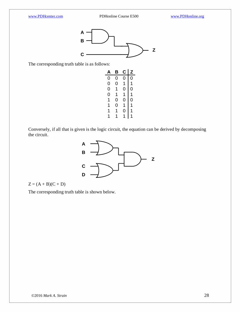
For example, the following equation is easily made into a circuit using combinational logic:
Z = AB + C
A
B
C X
D
www.PDHcenter.com PDHonline Course E500 www.PDHonline.org
©2016 Mark A. Strain 28
The corresponding truth table is as follows:
A B C Z
0 0 0 0 0 0 1 1 0 1 0 0
0 1 1 1 1 0 0 0 1 0 1 1
1 1 0 1 1 1 1 1
Conversely, if all that is given is the logic circuit, the equation can be derived by decomposing
the circuit.
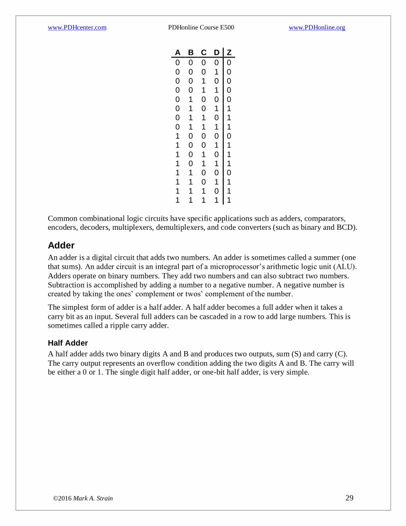
Z = (A + B)(C + D)
The corresponding truth table is shown below.
A
B
CZ
A
B
Z
C
D
www.PDHcenter.com PDHonline Course E500 www.PDHonline.org
©2016 Mark A. Strain 29
A B C D Z
0 0 0 0 0
0 0 0 1 0 0 0 1 0 0 0 0 1 1 0
0 1 0 0 0 0 1 0 1 1 0 1 1 0 1
0 1 1 1 1 1 0 0 0 0 1 0 0 1 1
1 0 1 0 1 1 0 1 1 1 1 1 0 0 0
1 1 0 1 1 1 1 1 0 1 1 1 1 1 1
Common combinational logic circuits have specific applications such as adders, comparators, encoders, decoders, multiplexers, demultiplexers, and code converters (such as binary and BCD).
Adder
An adder is a digital circuit that adds two numbers. An adder is sometimes called a summer (one
that sums). An adder circuit is an integral part of a microprocessor’s arithmetic logic unit (ALU).
Adders operate on binary numbers. They add two numbers and can also subtract two numbers.
Subtraction is accomplished by adding a number to a negative number. A negative number is created by taking the ones’ complement or twos’ complement of the number.
The simplest form of adder is a half adder. A half adder becomes a full adder when it takes a
carry bit as an input. Several full adders can be cascaded in a row to add large numbers. This is sometimes called a ripple carry adder.
Half Adder
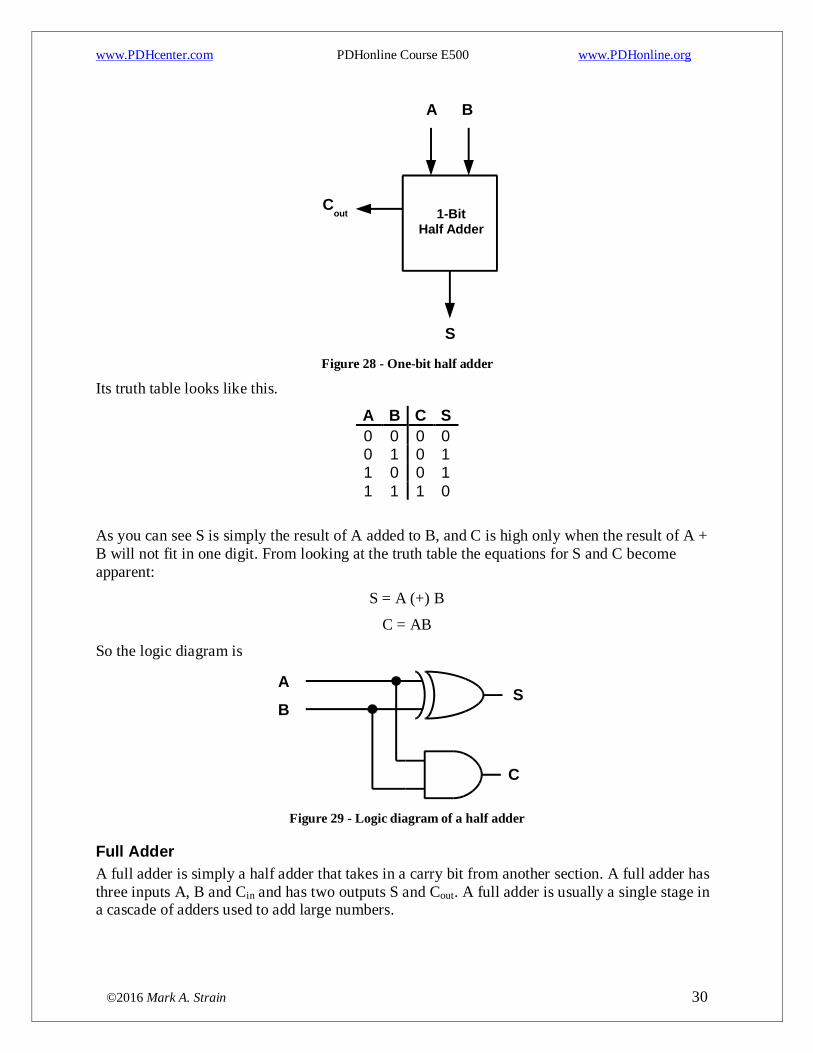
A half adder adds two binary digits A and B and produces two outputs, sum (S) and carry (C).
The carry output represents an overflow condition adding the two digits A and B. The carry will be either a 0 or 1. The single digit half adder, or one-bit half adder, is very simple.
www.PDHcenter.com PDHonline Course E500 www.PDHonline.org
©2016 Mark A. Strain 30
Figure 28 - One-bit half adder
Its truth table looks like this.
A B C S
0 0 0 0 0 1 0 1 1 0 0 1
1 1 1 0
As you can see S is simply the result of A added to B, and C is high only when the result of A +
B will not fit in one digit. From looking at the truth table the equations for S and C become
apparent:
S = A (+) B
C = AB
So the logic diagram is
Figure 29 - Logic diagram of a half adder
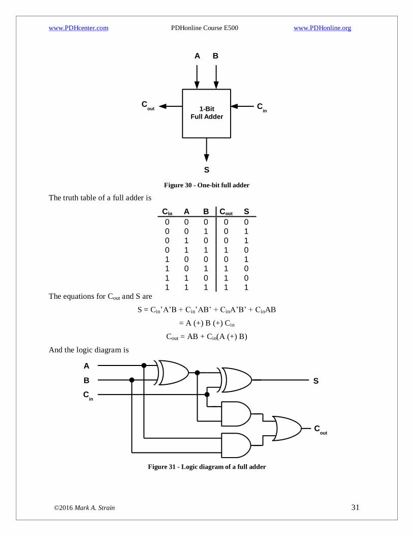
Full Adder
A full adder is simply a half adder that takes in a carry bit from another section. A full adder has
three inputs A, B and Cin and has two outputs S and Cout. A full adder is usually a single stage in a cascade of adders used to add large numbers.
A
1-BitHalf Adder
Cout
B
S
SA
B
C
www.PDHcenter.com PDHonline Course E500 www.PDHonline.org
©2016 Mark A. Strain 31
Figure 30 - One-bit full adder
The truth table of a full adder is
Cin A B Cout S
0 0 0 0 0 0 0 1 0 1 0 1 0 0 1
0 1 1 1 0 1 0 0 0 1 1 0 1 1 0
1 1 0 1 0 1 1 1 1 1
The equations for Cout and S are
S = Cin’A’B + Cin’AB’ + CinA’B’ + CinAB
= A (+) B (+) Cin
Cout = AB + Cin(A (+) B)
And the logic diagram is
Figure 31 - Logic diagram of a full adder
A
1-BitFull Adder
Cout
B
S
Cin
S
A
B
Cout
Cin
www.PDHcenter.com PDHonline Course E500 www.PDHonline.org
©2016 Mark A. Strain 32
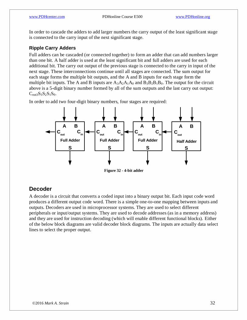
In order to cascade the adders to add larger numbers the carry output of the least significant stage
is connected to the carry input of the next significant stage.
Ripple Carry Adders
Full adders can be cascaded (or connected together) to form an adder that can add numbers larger
than one bit. A half adder is used at the least significant bit and full adders are used for each
additional bit. The carry out output of the previous stage is connected to the carry in input of the
next stage. These interconnections continue until all stages are connected. The sum output for
each stage forms the multiple bit outputs, and the A and B inputs for each stage form the
multiple bit inputs. The A and B inputs are A3A2A1A0 and B3B2B1B0. The output for the circuit
above is a 5-digit binary number formed by all of the sum outputs and the last carry out output: Cout3S3S2S1S0.
In order to add two four-digit binary numbers, four stages are required:
Figure 32 - 4-bit adder
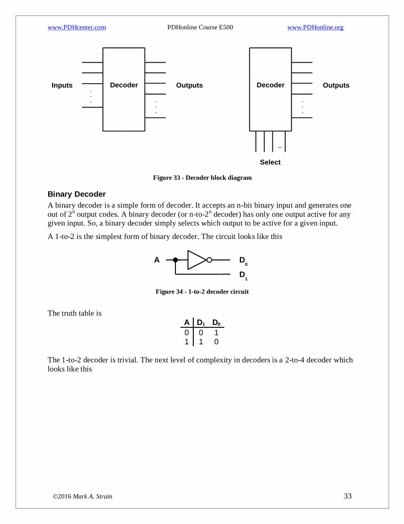
Decoder
A decoder is a circuit that converts a coded input into a binary output bit. Each input code word
produces a different output code word. There is a simple one-to-one mapping between inputs and
outputs. Decoders are used in microprocessor systems. They are used to select different
peripherals or input/output systems. They are used to decode addresses (as in a memory address)
and they are used for instruction decoding (which will enable different functional blocks). Either
of the below block diagrams are valid decoder block diagrams. The inputs are actually data select
lines to select the proper output.
A
Half Adder
Cout
B
S
A
Full Adder
Cout
B
S
Cin
A
Full Adder
Cout
B
S
Cin
A
Full Adder
Cout
B
S
Cin
www.PDHcenter.com PDHonline Course E500 www.PDHonline.org
©2016 Mark A. Strain 33
Figure 33 - Decoder block diagram
Binary Decoder
A binary decoder is a simple form of decoder. It accepts an n-bit binary input and generates one
out of 2n output codes. A binary decoder (or n-to-2
n decoder) has only one output active for any
given input. So, a binary decoder simply selects which output to be active for a given input.
A 1-to-2 is the simplest form of binary decoder. The circuit looks like this
Figure 34 - 1-to-2 decoder circuit
The truth table is
A D1 D0
0 0 1 1 1 0
The 1-to-2 decoder is trivial. The next level of complexity in decoders is a 2-to-4 decoder which
looks like this
Decoder
.
.
.
.
.
.
OutputsInputs Decoder
.
.
.
Outputs
Select
...
A D0
D1
www.PDHcenter.com PDHonline Course E500 www.PDHonline.org
©2016 Mark A. Strain 34
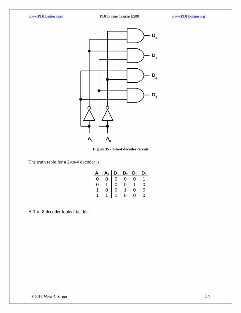
Figure 35 - 2-to-4 decoder circuit
The truth table for a 2-to-4 decoder is
A1 A0 D3 D2 D1 D0
0 0 0 0 0 1
0 1 0 0 1 0 1 0 0 1 0 0 1 1 1 0 0 0
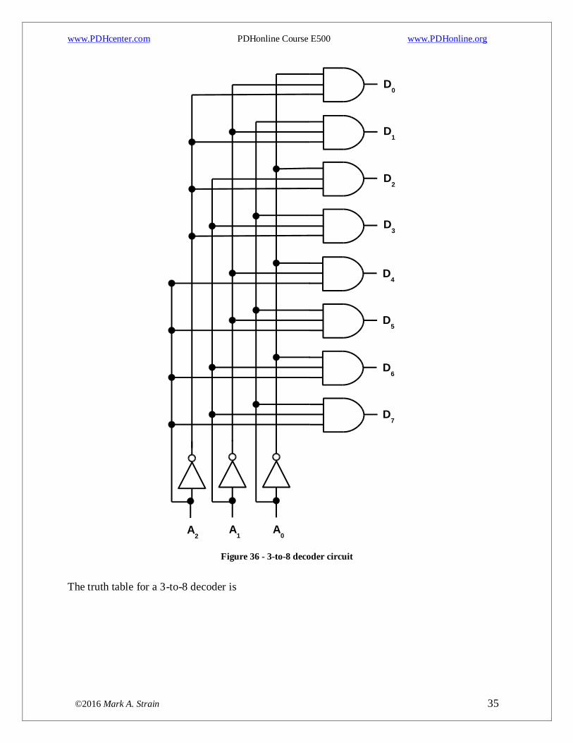
A 3-to-8 decoder looks like this
D0
A0
A1
D1
D2
D3
www.PDHcenter.com PDHonline Course E500 www.PDHonline.org
©2016 Mark A. Strain 35
Figure 36 - 3-to-8 decoder circuit
The truth table for a 3-to-8 decoder is
D0
A0
A1
D1
D2
D3
A2
D4
D5
D6
D7
www.PDHcenter.com PDHonline Course E500 www.PDHonline.org
©2016 Mark A. Strain 36
A2 A1 A0 D7 D6 D5 D4 D3 D2 D1 D0
0 0 0 0 0 0 0 0 0 0 1 0 0 1 0 0 0 0 0 0 1 0 0 1 0 0 0 0 0 0 1 0 0
0 1 1 0 0 0 0 1 0 0 0 1 0 0 0 0 0 1 0 0 0 0 1 0 1 0 0 1 0 0 0 0 0
1 1 0 0 1 0 0 0 0 0 0 1 1 1 1 0 0 0 0 0 0 0
A 3-to-8 decoder is commonly packaged into a 74138 part (a common digital integrated circuit).
The 74138 decoder is ideally suited for high speed memory chip select address decoding. The
decoder chip is used to select between multiple memory chips or other peripherals that share the
same memory bus. Using a decoder chip multiple devices, like memory chips, network
controllers, etc., can share the same address and data bus. The outputs of the decoder chip will be
connected to the chip select of each device, so only one device is electrically connected to the
bus at a time.
The output code for a binary decoder is simply a "1" that “walks” down the output pins as the
input binary code increases. Different versions exist. Some have enable pins that will not
produce any outputs unless the enable pin (or pins) are active. Other versions have all of the
outputs inverted which would produce a code in which all of the bits are inverted.
BCD to Seven-Segment Decoder
BCD (or binary coded decimal) is a type of binary code that encodes decimal digits into a fixed
group of binary digits. For example, the decimal digits 0-9 would be represented by 4 binary bits.
To represent a four-digit decimal number, 16 binary bits would be necessary:
2 5 9 7 0010 0101 1001 0111
So, the decimal number 2597 would be represented in BCD code as 0010010110010111.
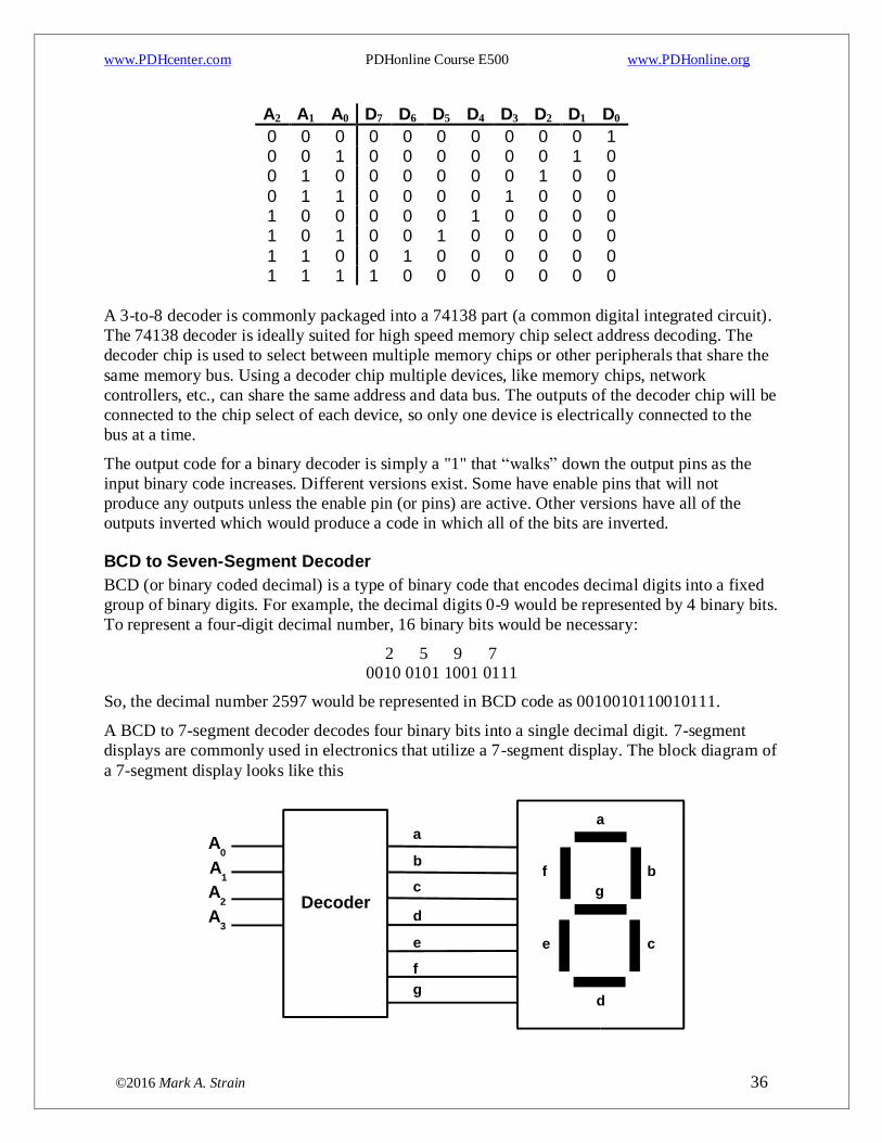
A BCD to 7-segment decoder decodes four binary bits into a single decimal digit. 7-segment
displays are commonly used in electronics that utilize a 7-segment display. The block diagram of
a 7-segment display looks like this
Decoder
a
b
d
f
ce
g
a
b
c
d
e
f
g
A0
A1
A2
A3
www.PDHcenter.com PDHonline Course E500 www.PDHonline.org
©2016 Mark A. Strain 37
Figure 37 - BCD to 7-segment display decoder
The truth table for the above BCD decoder will look like this
A3 A2 A1 A0 a b c d e f g
0 0 0 0 1 1 1 1 1 1 0 0 0 0 1 0 1 1 0 0 0 0 0 0 1 0 1 1 0 1 1 0 1
0 0 1 1 1 1 1 1 0 0 1 0 1 0 0 0 1 1 0 0 1 1 0 1 0 1 1 0 1 1 0 1 1
0 1 1 0 0 0 1 1 1 1 0 0 1 1 1 1 1 1 0 0 0 0 1 0 0 0 1 1 1 1 1 1 1
1 0 0 1 1 1 1 0 0 1 1 1 0 1 0 0 0 0 0 0 0 0 1 0 1 1 0 0 0 0 0 0 0
1 1 0 0 0 0 0 0 0 0 0 1 1 0 1 0 0 0 0 0 0 0 1 1 1 0 0 0 0 0 0 0 0
1 1 1 1 0 0 0 0 0 0 0
These BCD decoders can be cascaded so that any number of segments can be used to represent a
large decimal number.
Encoder
An encoder performs the opposite operation as a decoder. An encoder encodes an input code to
produce an encoded output.
A binary decoder takes n inputs and produces 2n outputs (n to 2
n), so an encoder takes 2
n inputs
and produces n outputs. For example, a 4-to-2 encoder takes 4 inputs and produces 2 outputs.
A3 A2 A1 A0 E1 E0
0 0 0 1 0 0 0 0 1 0 0 1 0 1 0 0 1 0
1 0 0 0 1 1
The above truth table produces the following output equations:
E0 = A1 + A3
E1 = A2 + A3
www.PDHcenter.com PDHonline Course E500 www.PDHonline.org
©2016 Mark A. Strain 38
Figure 38 - 4-to-2 encoder
The problem with this 4-to-2 encoder is that if more than one input is a “1” then the encoder does
not work properly. In this design if A2 and A3 are a “1” then the output would be E1E0 = 11
(which is the same result as an input of 1000). Also, an output of 00 is generated when all of its
inputs are “0” which is the same result as when the input is 0001. The solution to these problems
is to use a priority encoder.
Priority Encoder
A priority encoder solves the problems of a simple binary encoder by allocating a priority level
to each input. The output of a priority encoder corresponds to the currently active input which
has the highest priority. When an input has multiple “1s” the highest priority takes precedence
and all other inputs are ignored.
An example of a priority encoder is (where the Xs are “don’t cares”):
A3 A2 A1 A0 E1 E0
0 0 0 1 0 0
0 0 1 X 0 1 0 1 X X 1 0 1 X X X 1 1
So, from the truth table, the equations for E0 and E1 are
E0 = A3’A2’A1 + A3
E1 = A3’A2 + A3
And by using the property AB' + B = A + B, then the equations become
E0 = A2’A1 + A3
E1 = A2 + A3
And the logic diagram becomes
E0
A0
A1
A2
A3
E1
E0
A0
A1
A2
A3
E1
www.PDHcenter.com PDHonline Course E500 www.PDHonline.org
©2016 Mark A. Strain 39
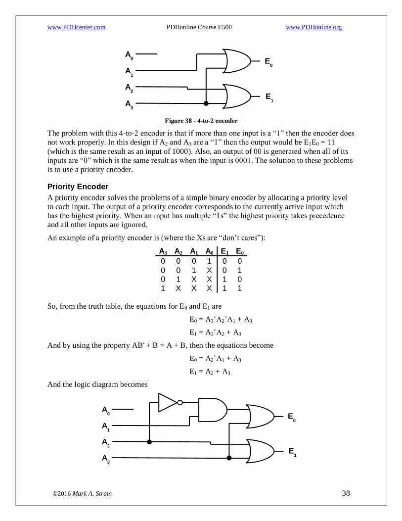
Figure 39 - 4-to-2 priority encoder
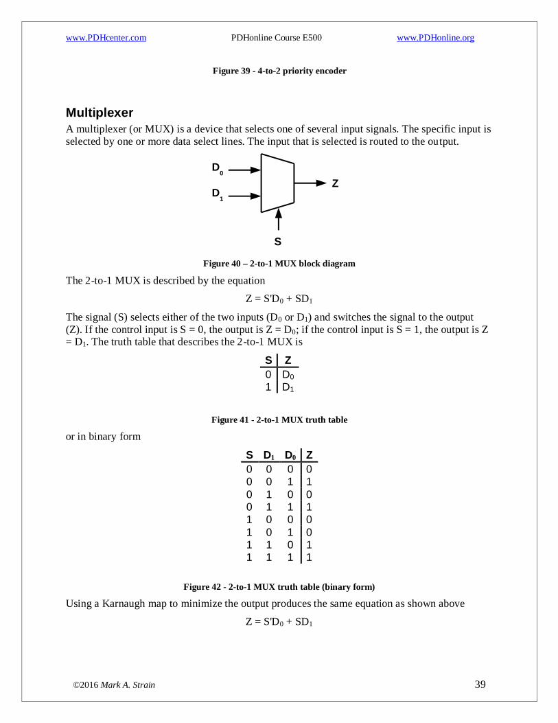
Multiplexer
A multiplexer (or MUX) is a device that selects one of several input signals. The specific input is
selected by one or more data select lines. The input that is selected is routed to the output.
Figure 40 – 2-to-1 MUX block diagram
The 2-to-1 MUX is described by the equation
Z = S'D0 + SD1
The signal (S) selects either of the two inputs (D0 or D1) and switches the signal to the output
(Z). If the control input is S = 0, the output is Z = D0; if the control input is S = 1, the output is Z = D1. The truth table that describes the 2-to-1 MUX is
S Z
0 D0 1 D1
Figure 41 - 2-to-1 MUX truth table
or in binary form
S D1 D0 Z
0 0 0 0 0 0 1 1
0 1 0 0 0 1 1 1 1 0 0 0
1 0 1 0 1 1 0 1 1 1 1 1
Figure 42 - 2-to-1 MUX truth table (binary form)
Using a Karnaugh map to minimize the output produces the same equation as shown above
Z = S'D0 + SD1
D0
D1
S
Z
www.PDHcenter.com PDHonline Course E500 www.PDHonline.org
©2016 Mark A. Strain 40
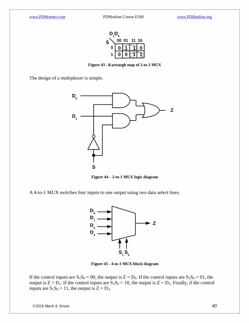
Figure 43 - Karnaugh map of 2-to-1 MUX
The design of a multiplexer is simple.
Figure 44 – 2-to-1 MUX logic diagram
A 4-to-1 MUX switches four inputs to one output using two data select lines.
Figure 45 - 4-to-1 MUX block diagram
If the control inputs are S1S0 = 00, the output is Z = D0. If the control inputs are S1S0 = 01, the
output is Z = D1. If the control inputs are S1S0 = 10, the output is Z = D2. Finally, if the control
inputs are S1S0 = 11, the output is Z = D3.
0 1 1 0
00 01 11 10
0
1
S
0 0 1 1
D1D
0
Z
D0
S
D1
D0
D1
ZD2
D3
S1S
0
www.PDHcenter.com PDHonline Course E500 www.PDHonline.org
©2016 Mark A. Strain 41
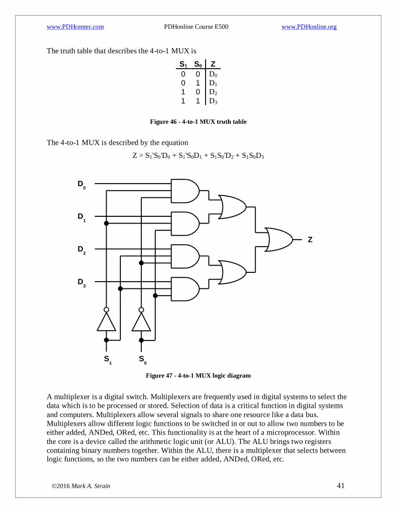
The truth table that describes the 4-to-1 MUX is
S1 S0 Z
0 0 D0
0 1 D1
1 0 D2
1 1 D3
Figure 46 - 4-to-1 MUX truth table
The 4-to-1 MUX is described by the equation
Z = S1'S0'D0 + S1'S0D1 + S1S0'D2 + S1S0D3
Figure 47 - 4-to-1 MUX logic diagram
A multiplexer is a digital switch. Multiplexers are frequently used in digital systems to select the
data which is to be processed or stored. Selection of data is a critical function in digital systems
and computers. Multiplexers allow several signals to share one resource like a data bus.
Multiplexers allow different logic functions to be switched in or out to allow two numbers to be
either added, ANDed, ORed, etc. This functionality is at the heart of a microprocessor. Within
the core is a device called the arithmetic logic unit (or ALU). The ALU brings two registers
containing binary numbers together. Within the ALU, there is a multiplexer that selects between logic functions, so the two numbers can be either added, ANDed, ORed, etc.
Z
D0
D1
S0
S1
D2
D3
www.PDHcenter.com PDHonline Course E500 www.PDHonline.org
©2016 Mark A. Strain 42
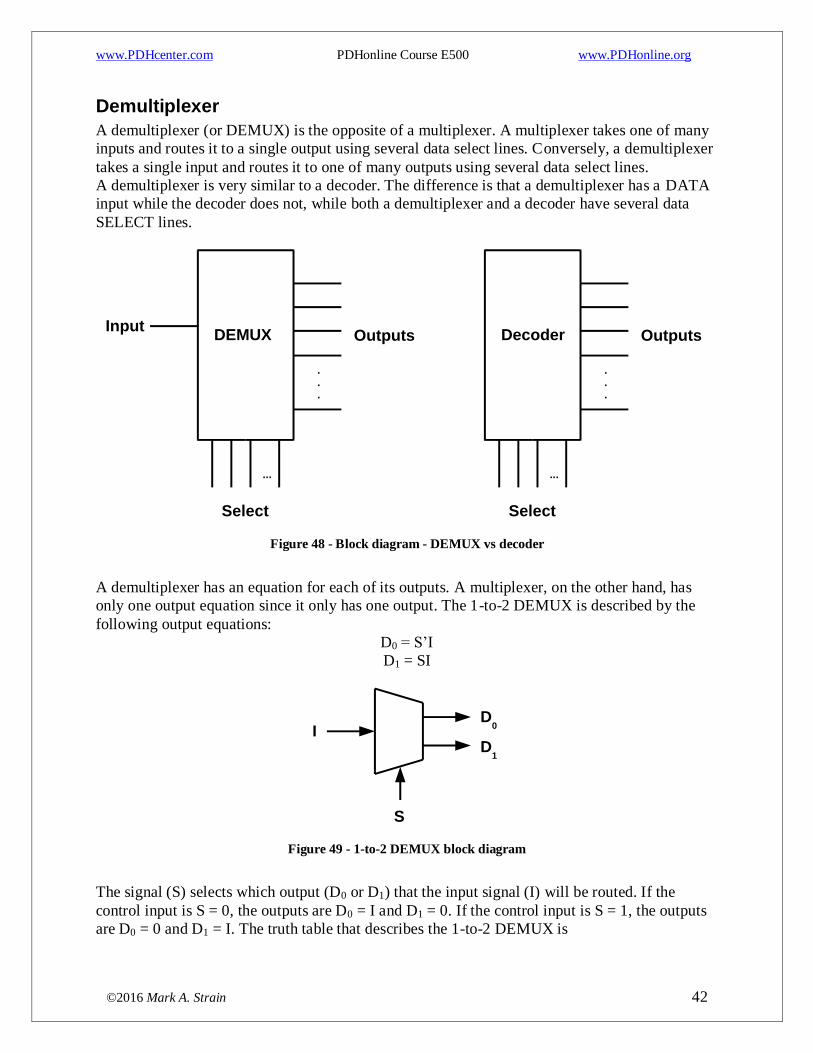
Demultiplexer
A demultiplexer (or DEMUX) is the opposite of a multiplexer. A multiplexer takes one of many
inputs and routes it to a single output using several data select lines. Conversely, a demultiplexer
takes a single input and routes it to one of many outputs using several data select lines.
A demultiplexer is very similar to a decoder. The difference is that a demultiplexer has a DATA
input while the decoder does not, while both a demultiplexer and a decoder have several data
SELECT lines.
Figure 48 - Block diagram - DEMUX vs decoder
A demultiplexer has an equation for each of its outputs. A multiplexer, on the other hand, has
only one output equation since it only has one output. The 1-to-2 DEMUX is described by the
following output equations:
D0 = S’I
D1 = SI
Figure 49 - 1-to-2 DEMUX block diagram
The signal (S) selects which output (D0 or D1) that the input signal (I) will be routed. If the
control input is S = 0, the outputs are D0 = I and D1 = 0. If the control input is S = 1, the outputs
are D0 = 0 and D1 = I. The truth table that describes the 1-to-2 DEMUX is
Decoder
.
.
.
Outputs
Select
...
DEMUX
.
.
.
Outputs
Select
...
Input
D0
D1
S
I
www.PDHcenter.com PDHonline Course E500 www.PDHonline.org
©2016 Mark A. Strain 43
S D1 D0
0 0 I
1 I 0
or, in binary form
S I D1 D0
0 0 0 0 0 1 0 1
1 0 0 0 1 1 1 0
Figure 50 - 1-to-2 DEMUX truth table
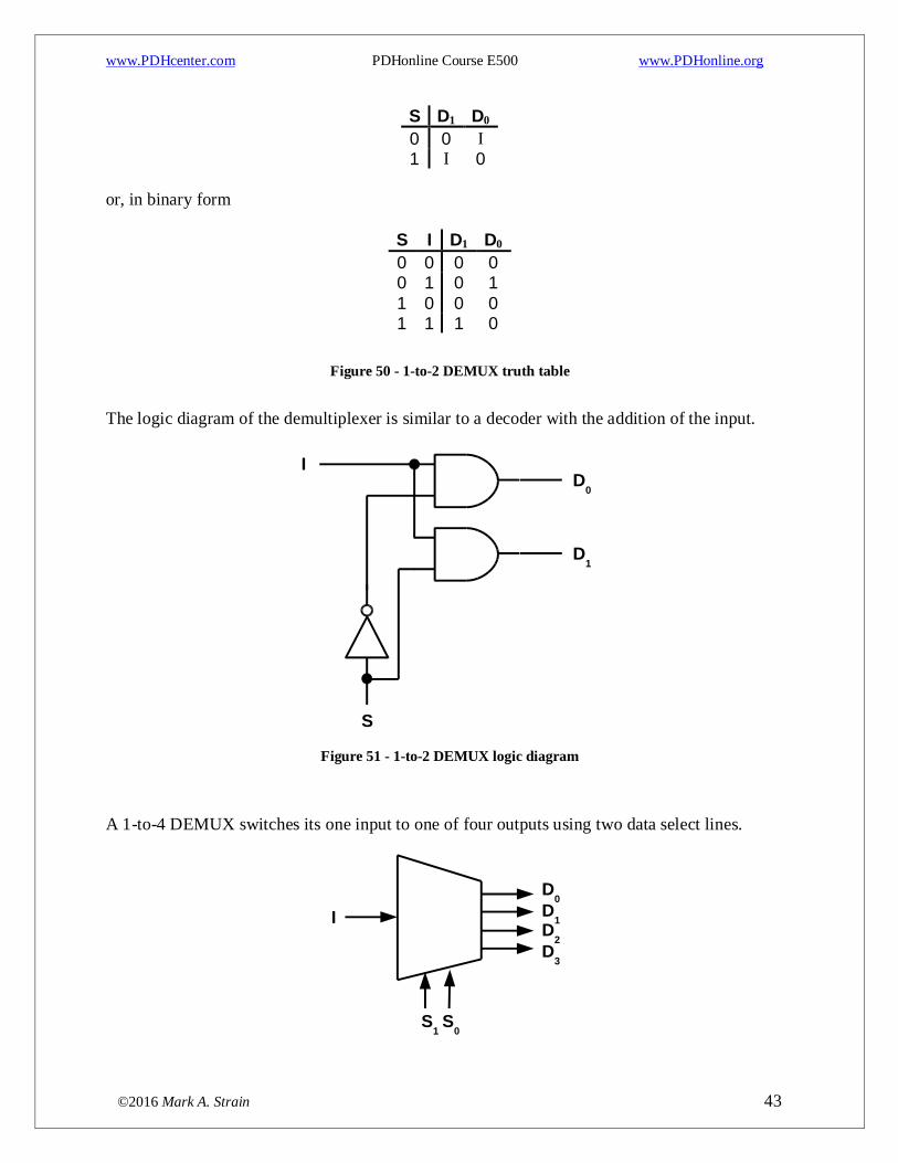
The logic diagram of the demultiplexer is similar to a decoder with the addition of the input.
Figure 51 - 1-to-2 DEMUX logic diagram
A 1-to-4 DEMUX switches its one input to one of four outputs using two data select lines.
D0
S
D1
I
D0
D1I
D2
D3
S1S
0
www.PDHcenter.com PDHonline Course E500 www.PDHonline.org
©2016 Mark A. Strain 44
Figure 52 - 1-to-4 DEMUX block diagram
If the control inputs are S1S0 = 00, the outputs are D0 = I, D1 = 0, D2 = 0, D3 = 0. If the control
inputs are S1S0 = 01, the outputs are D0 = 0, D1 = I, D2 = 0, D3 = 0. If the control inputs are S1S0
= 10, the outputs are D0 = 0, D1 = 0, D2 = I, D3 = 0. If the control inputs are S1S1 = 11, the outputs are D0 = 0, D1 = 0, D2 = 0, D3 = I.
The truth table that describes the 1-to-4 DEMUX is
S1 S0 D3 D2 D1 D0
0 0 0 0 0 I
0 1 0 0 I 0 1 0 0 I 0 0 1 1 I 0 0 0
or, in binary form
S1 S0 I D3 D2 D1 D0
0 0 0 0 0 0 0
0 0 1 0 0 0 1 0 1 0 0 0 0 0 0 1 1 0 0 1 0
1 0 0 0 0 0 0 1 0 1 0 1 0 0 1 1 0 0 0 0 0 1 1 1 1 0 0 0
The 1-to-4 DEMUX is described by the following output equations
D0 = S1’S0’I
D1 = S1’S0I
D2 = S1S0’I
D3 = S1S0I
www.PDHcenter.com PDHonline Course E500 www.PDHonline.org
©2016 Mark A. Strain 45
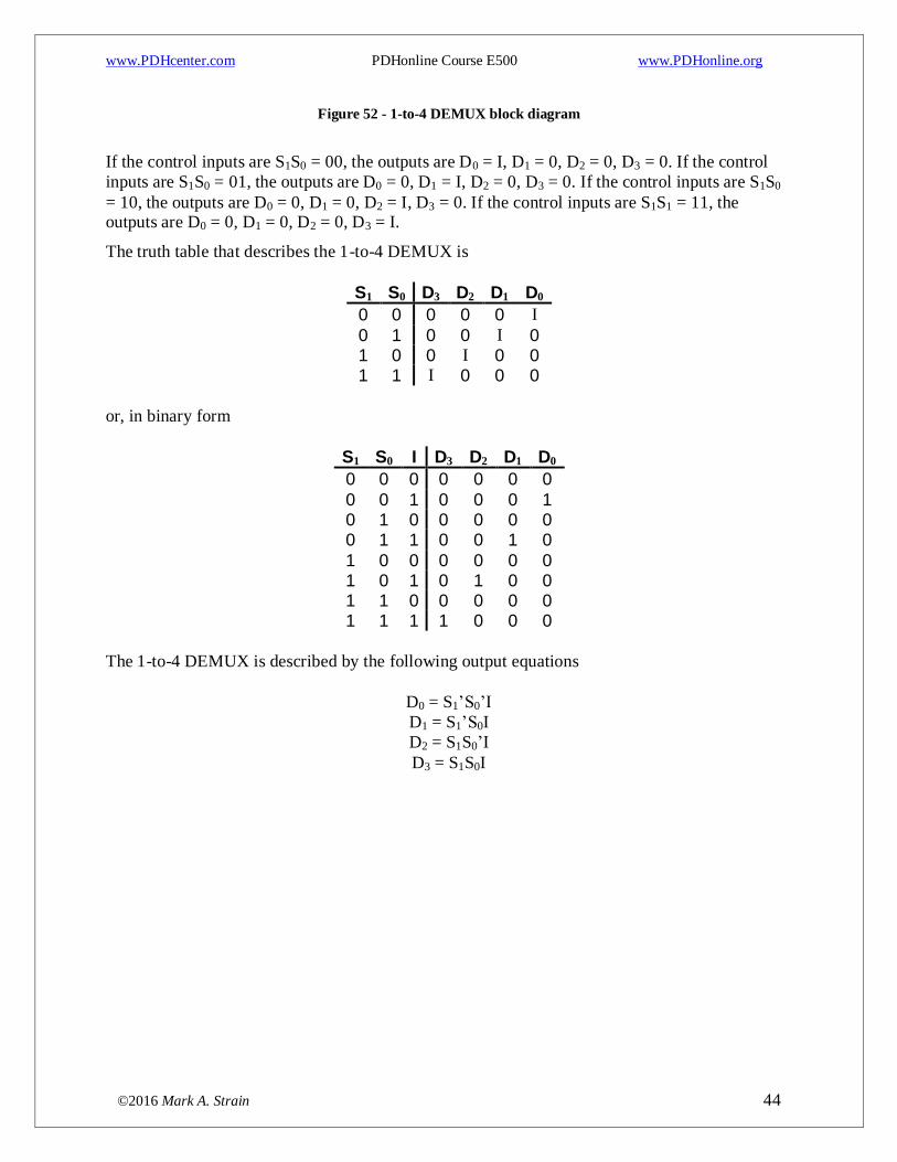
Figure 53 - 1-to-4 DEMUX logic diagram
The following table shows the similarities and differences between a DEMUX and a decoder and
a MUX and an encoder.
Demultiplexer Decoder Multiplexer Encoder
#inputs # outputs
1 data input
n data select lines
2n outputs
0 data inputs
n data select lines
2n outputs
2n inputs
n data select lines
1 output
2n inputs
0 data select lines
n outputs
Description Connects data input
to the data output
Selects one of the 2n
outputs based on the
n data select lines
Routes one of the 2n
inputs to the output
based on the n data
select lines
Converts the input to
a binary-coded
output
Complement of Multiplexer Encoder Demultiplexer Decoder
Table 1 - DEMUX vs Decoder, MUX vs Encoder
D0
D1
S0
S1
D2
D3
I
www.PDHcenter.com PDHonline Course E500 www.PDHonline.org
©2016 Mark A. Strain 46
Summary Digital circuits have infiltrated every part of modern society. Life would definitely be different
without their existence. The transistor is the fundamental building block in all digital circuits. Its
miniaturization has allowed for the explosive growth in the complexity of digital circuits and in
computing power. The binary numbering system is ideal to represent the inner workings of
digital circuits since transistors can be driven high (or logic 1) or driven low (or logic 0).
Transistors are organized into logic gates, the most basic being the AND, OR and NOT gates.
With these fundamental gates, all other gates are built. Combinational logic is formed when
several gates are connected together to form a more complicated circuit. With this combinational
logic, adders can be built as well as encoders, decoders, multiplexers and demultiplexers.
www.PDHcenter.com PDHonline Course E500 www.PDHonline.org
©2016 Mark A. Strain 47
References
1. “Adder (electronics) – Wikipedia, the Free Encyclopedia.” Visited 20 July 2015
<https://en.wikipedia.org/wiki/Adder_(electronics)>
2. “Basics of Digital Logic Design, Presentation D.” visited 19 December 2014
<http://web.cse.ohio-
state.edu/~teodores/download/teaching/cse675.au08/Cse675.02.D.LogicDesign_part1.pdf
>
3. “Digital Logic Design.” visited 19 December 2014
<http://american.cs.ucdavis.edu/academic/ecs154a.sum14/postscript/cosc205.pdf>
4. “Digital Logic Design, Lecture Schedule.” 4 September 2013
<http://www.ece.rutgers.edu/~marsic/Teaching/DLD/syllabus.html>
5. “Karnaugh Map – Wikipedia, the Free Encyclopedia.” Visited 26 July 2015
<https://en.wikipedia.org/wiki/Karnaugh_map>
6. Roth, Charles H. Jr., Fundamentals of Logic Design, 3rd ed., West Publishing Co., St.
Paul, MN, 1985.
7. “NAND Logic – Wikipedia, the Free Encyclopedia.” visited 28 October 2014
<http://en.wikipedia.org/wiki/NAND_logic>