Embed Size (px)
Citation preview

NuDAQ® ACL-7120A
Digital I/O & Timer/Counter Card User’s Guide
Copyright 1995, 2003 ADLINK TECHNOLOGY INC.
All Rights Reserved.
Manual Rev. 1.00: May 30, 2003
Part No: 50-11031-100
The information in this document is subject to change without prior notice in order to improve reliability, design, and function and does not represent a commitment on the part of the manufacturer.
In no event will the manufacturer be liable for direct, indirect, special, incidental, or consequential damages arising out of the use or inability to use the product or documentation, even if advised of the possibility of such damages.
This document contains proprietary information protected by copyright. All rights are reserved. No part of this manual may be reproduced by any mechanical, electronic, or other means in any form without prior written permission of the manufacturer.
Trademarks
NuDAQ, ACL-7120A is registered trademarks of ADLINK TECHNOLOGY INC.
Other product names mentioned herein are used for identification purposes only and may be trademarks and/or registered trademarks of their respective companies.
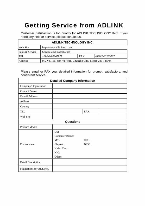
Getting Service from ADLINK Customer Satisfaction is top priority for ADLINK TECHNOLOGY INC. If you need any help or service, please contact us.
ADLINK TECHNOLOGY INC. Web Site http://www.adlinktech.com Sales & Service [email protected] TEL +886-2-82265877 FAX +886-2-82265717 Address 9F, No. 166, Jian Yi Road, Chungho City, Taipei, 235 Taiwan
Please email or FAX your detailed information for prompt, satisfactory, and consistent service.
Detailed Company Information Company/Organization
Contact Person
E-mail Address
Address
Country
TEL FAX
Web Site
Questions Product Model
Environment
OS: Computer Brand: M/B: CPU: Chipset: BIOS: Video Card: NIC: Other:
Detail Description
Suggestions for ADLINK
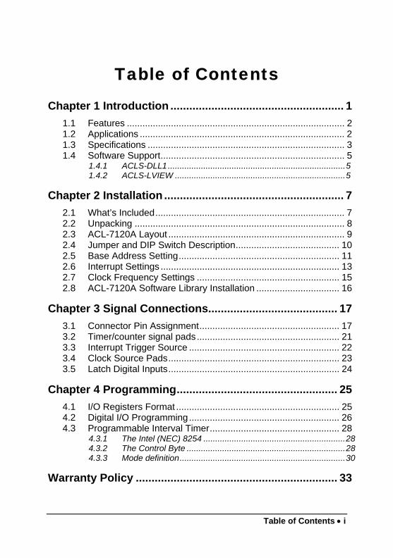
Table of Contents • i
Table of Contents
Chapter 1 Introduction ....................................................... 1 1.1 Features .................................................................................... 2 1.2 Applications ............................................................................... 2 1.3 Specifications ............................................................................ 3 1.4 Software Support....................................................................... 5
1.4.1 ACLS-DLL1...........................................................................5 1.4.2 ACLS-LVIEW ........................................................................5
Chapter 2 Installation ......................................................... 7 2.1 What’s Included......................................................................... 7 2.2 Unpacking ................................................................................. 8 2.3 ACL-7120A Layout .................................................................... 9 2.4 Jumper and DIP Switch Description........................................ 10 2.5 Base Address Setting.............................................................. 11 2.6 Interrupt Settings ..................................................................... 13 2.7 Clock Frequency Settings ....................................................... 15 2.8 ACL-7120A Software Library Installation ................................ 16
Chapter 3 Signal Connections......................................... 17 3.1 Connector Pin Assignment...................................................... 17 3.2 Timer/counter signal pads....................................................... 21 3.3 Interrupt Trigger Source .......................................................... 22 3.4 Clock Source Pads.................................................................. 23 3.5 Latch Digital Inputs.................................................................. 24
Chapter 4 Programming................................................... 25 4.1 I/O Registers Format ............................................................... 25 4.2 Digital I/O Programming.......................................................... 26 4.3 Programmable Interval Timer.................................................. 28
4.3.1 The Intel (NEC) 8254 ............................................................28 4.3.2 The Control Byte ...................................................................28 4.3.3 Mode definition......................................................................30
Warranty Policy ................................................................ 33
ii • How to Use This Guide
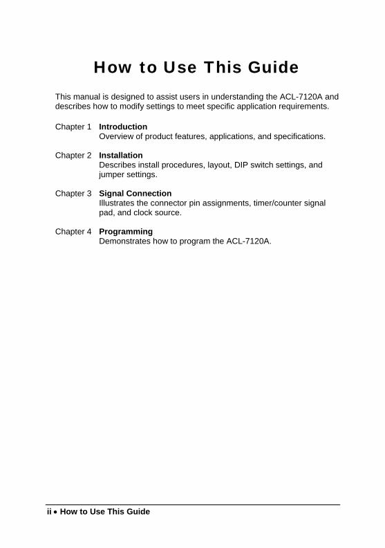
How to Use This Guide This manual is designed to assist users in understanding the ACL-7120A and describes how to modify settings to meet specific application requirements.
Chapter 1 Introduction Overview of product features, applications, and specifications.
Chapter 2 Installation Describes install procedures, layout, DIP switch settings, and jumper settings.
Chapter 3 Signal Connection
Illustrates the connector pin assignments, timer/counter signal pad, and clock source.
Chapter 4 Programming
Demonstrates how to program the ACL-7120A.
Introduction • 1
1
Introduction
The ACL-7120A digital I/O and counter/timer card consists of 32 digital input, 32 digital output, and 4 timer/counter channels. All digital input/output channels are TTL/DTL compatible. The most outstanding feature of the ACL-7120A is that it is fully hardware and software compatible with both the ADLINK ACL-7120 and Advantech PCL-720 cards.
The ACL-7120A supports additional daughter boards like the ACLD-9182 and ACLD-9185 cards. The ACLD-9182 is a 16 channel opto-isolated digital board for inputting digital data to the ACL-7120A when ground isolation is required. The ACLD-9185 is a 16-channel relay output board that can be driven by digital outputs from the ACL-7120A.
Up to four programmable interval timers (8254) are provided to add timer and counter functionalities. To efficiently use the counter, three frequency sources (10kHz, 100kHz, and 1MHz) are supported for the input of each counter. In addition, the sources can also be doubled (X2), halved (1/2) or quartered (1/4) through jumper settings to give more flexibility for different frequency timer and counter applications.
An optional timer/counter chip is used to support a timer pacer that can generate periodic interrupts. Also, an event counter can be used for external event counting.
2 • Introduction
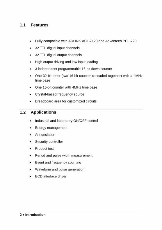
1.1 Features
• Fully compatible with ADLINK ACL-7120 and Advantech PCL-720
• 32 TTL digital input channels
• 32 TTL digital output channels
• High output driving and low input loading
• 3 independent programmable 16-bit down counter
• One 32-bit timer (two 16-bit counter cascaded together) with a 4MHz time base
• One 16-bit counter with 4MHz time base
• Crystal-based frequency source
• Breadboard area for customized circuits
1.2 Applications
• Industrial and laboratory ON/OFF control
• Energy management
• Annunciation
• Security controller
• Product test
• Period and pulse width measurement
• Event and frequency counting
• Waveform and pulse generation
• BCD interface driver
Introduction • 3
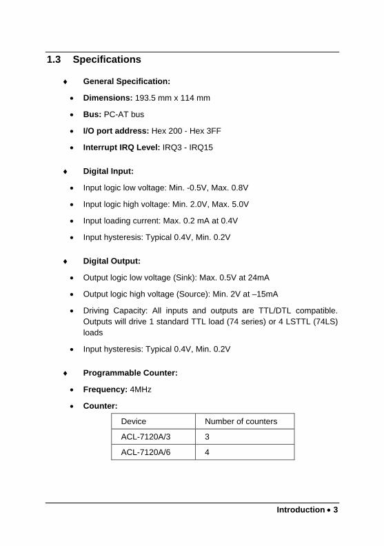
1.3 Specifications
♦ General Specification:
• Dimensions: 193.5 mm x 114 mm
• Bus: PC-AT bus
• I/O port address: Hex 200 - Hex 3FF
• Interrupt IRQ Level: IRQ3 - IRQ15
♦ Digital Input:
• Input logic low voltage: Min. -0.5V, Max. 0.8V
• Input logic high voltage: Min. 2.0V, Max. 5.0V
• Input loading current: Max. 0.2 mA at 0.4V
• Input hysteresis: Typical 0.4V, Min. 0.2V
♦ Digital Output:
• Output logic low voltage (Sink): Max. 0.5V at 24mA
• Output logic high voltage (Source): Min. 2V at –15mA
• Driving Capacity: All inputs and outputs are TTL/DTL compatible. Outputs will drive 1 standard TTL load (74 series) or 4 LSTTL (74LS) loads
• Input hysteresis: Typical 0.4V, Min. 0.2V
♦ Programmable Counter:
• Frequency: 4MHz
• Counter:
Device Number of counters
ACL-7120A/3 3
ACL-7120A/6 4
4 • Introduction
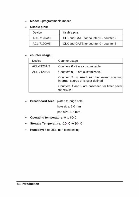
• Mode: 6 programmable modes
• Usable pins:
Device Usable pins
ACL-7120A/3 CLK and GATE for counter 0 - counter 2
ACL-7120A/6 CLK and GATE for counter 0 - counter 3
• counter usage :
Device Counter usage
ACL-7120A/3 Counters 0 - 2 are customizable
ACL-7120A/6 Counters 0 - 2 are customizable
Counter 3 is used as the event counting interrupt source or is user defined
Counters 4 and 5 are cascaded for timer pacer generation
• Breadboard Area: plated through hole:
hole size: 1.0 mm
pad size: 1.5 mm
• Operating temperature: 0 to 60°C
• Storage Temperature: -20° C to 80° C
• Humidity: 5 to 90%, non-condensing
Introduction • 5
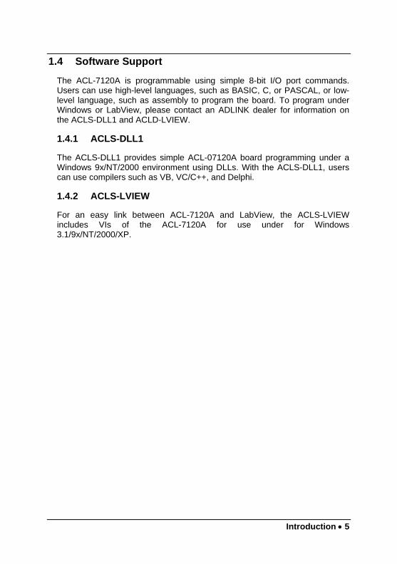
1.4 Software Support
The ACL-7120A is programmable using simple 8-bit I/O port commands. Users can use high-level languages, such as BASIC, C, or PASCAL, or low- level language, such as assembly to program the board. To program under Windows or LabView, please contact an ADLINK dealer for information on the ACLS-DLL1 and ACLD-LVIEW.
1.4.1 ACLS-DLL1
The ACLS-DLL1 provides simple ACL-07120A board programming under a Windows 9x/NT/2000 environment using DLLs. With the ACLS-DLL1, users can use compilers such as VB, VC/C++, and Delphi.
1.4.2 ACLS-LVIEW
For an easy link between ACL-7120A and LabView, the ACLS-LVIEW includes VIs of the ACL-7120A for use under for Windows 3.1/9x/NT/2000/XP.
Installation • 7
2
Installation
This chapter describes how to install the ACL-7120A. Please carefully review the unpacking information before removing the product. The jumper and switch settings for the ACL-7120A base address, clock sources, interrupt IRQ level, and IRQ trigger sources are specified below.
2.1 What’s Included
In addition to this User's Manual, the package includes the following items:
♦ ACL-7120A Digital I/O and Timer/Counter Card
♦ ADLINK CD
If any of these items is missing or damaged, contact the dealer the product was purchased. Save the shipping materials and carton to ship or store the product in the future.

8 • Installation
2.2 Unpacking
Your ACL-7120A card contains sensitive electronic components that can be easily damaged by static electricity.
Prepare a grounded anti-static mat. The operator should be wearing an anti-static wristband, grounded at the same point as the anti-static mat.
Inspect the card module carton for obvious damage. Shipping and handling may cause damage to the module. Be sure there is no obvious damage due to shipping and handing by examining the shipping box.
After opening the card module carton, extract the system module and place it only on a grounded anti-static surface, component side up.
Again inspecting the module for damage. Press down on all the socketed IC's to make sure they are properly seated. Do this only with the module place on a firm flat surface.
Note: DO NOT APPLY POWER TO THE CARD IF IT HAS BEEN DAMAGED.
You are now ready to install your ACL-7120A.
Installation • 9
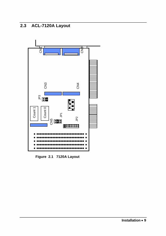
2.3 ACL-7120A Layout
Figure 2.1 7120A Layout
SW1
CN
1
CN
2
CN
3
CN
4
CN
5
JP1
JP2
JP3
Cou
nt 0
Cou
nt 1
● ●●●●●●●●●●●●●●●●●●●●●●●●●●●●●● ● ● ●●●●●●●●●●●●●●●●●●●●●●●●●●●●●● ● ● ●●●●●●●●●●●●●●●●●●●●●●●●●●●●●● ● ● ●●●●●●●●●●●●●●●●●●●●●●●●●●●●●● ● ● ●●●●●●●●●●●●●●●●●●●●●●●●●●●●●● ●
10 • Installation
2.4 Jumper and DIP Switch Description
The ACL-7120A channels and base addresses can be changed through jumper settings and DIP switches on the card. The ACL-7120A is pre-configured at the factory and should not need to be changed under normal circumstances.
A jumper switch is closed or "shorted" with the plastic cap inserted over two pins of the jumper. A jumper is open when the plastic cap inserted over one or no pin(s) of the jumper.
Installation • 11
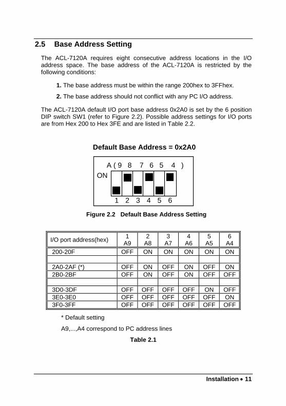
2.5 Base Address Setting
The ACL-7120A requires eight consecutive address locations in the I/O address space. The base address of the ACL-7120A is restricted by the following conditions:
1. The base address must be within the range 200hex to 3FFhex.
2. The base address should not conflict with any PC I/O address.
The ACL-7120A default I/O port base address 0x2A0 is set by the 6 position DIP switch SW1 (refer to Figure 2.2). Possible address settings for I/O ports are from Hex 200 to Hex 3FE and are listed in Table 2.2.
Default Base Address = 0x2A0
1 2 3 4 5 6
ONA ( 9 8 7 6 5 4 )
Figure 2.2 Default Base Address Setting
I/O port address(hex) 1 A9
2 A8
3 A7
4 A6
5 A5
6 A4
200-20F OFF ON ON ON ON ON 2A0-2AF (*) OFF ON OFF ON OFF ON 2B0-2BF OFF ON OFF ON OFF OFF 3D0-3DF OFF OFF OFF OFF ON OFF 3E0-3E0 OFF OFF OFF OFF OFF ON 3F0-3FF OFF OFF OFF OFF OFF OFF
* Default setting
A9,...,A4 correspond to PC address lines
Table 2.1
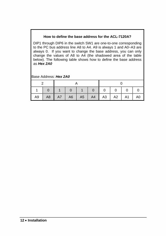
12 • Installation
How to define the base address for the ACL-7120A?
DIP1 through DIP6 in the switch SW1 are one-to-one corresponding to the PC bus address line A8 to A4. A9 is always 1 and A0~A3 are always 0. If you want to change the base address, you can only change the values of A8 to A4 (the shadowed area of the table below). The following table shows how to define the base address as Hex 2A0
Base Address: Hex 2A0
2 A 0
1 0 1 0 1 0 0 0 0 0
A9 A8 A7 A6 A5 A4 A3 A2 A1 A0
Installation • 13
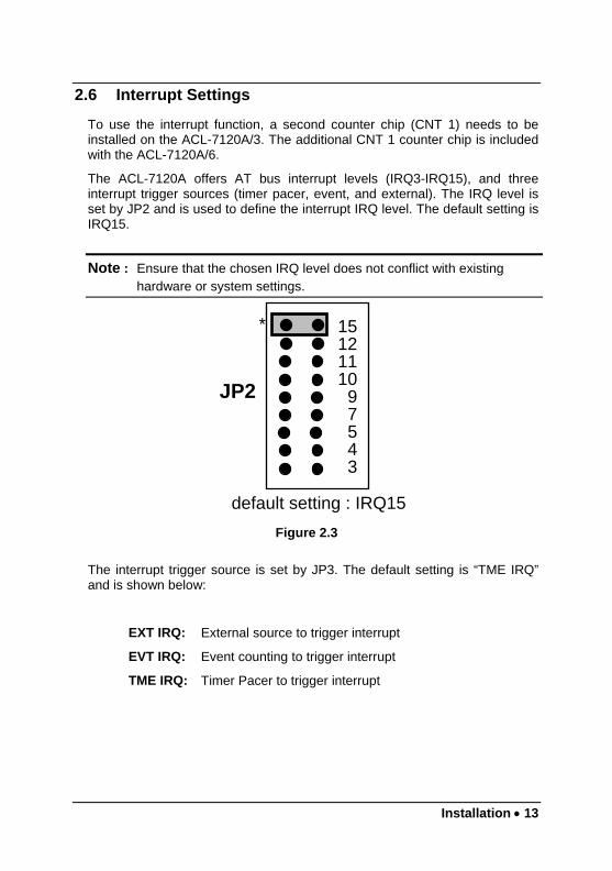
2.6 Interrupt Settings
To use the interrupt function, a second counter chip (CNT 1) needs to be installed on the ACL-7120A/3. The additional CNT 1 counter chip is included with the ACL-7120A/6.
The ACL-7120A offers AT bus interrupt levels (IRQ3-IRQ15), and three interrupt trigger sources (timer pacer, event, and external). The IRQ level is set by JP2 and is used to define the interrupt IRQ level. The default setting is IRQ15.
Note : Ensure that the chosen IRQ level does not conflict with existing hardware or system settings.
JP2
*
default setting : IRQ15
15121110 9 7 5 4 3
Figure 2.3
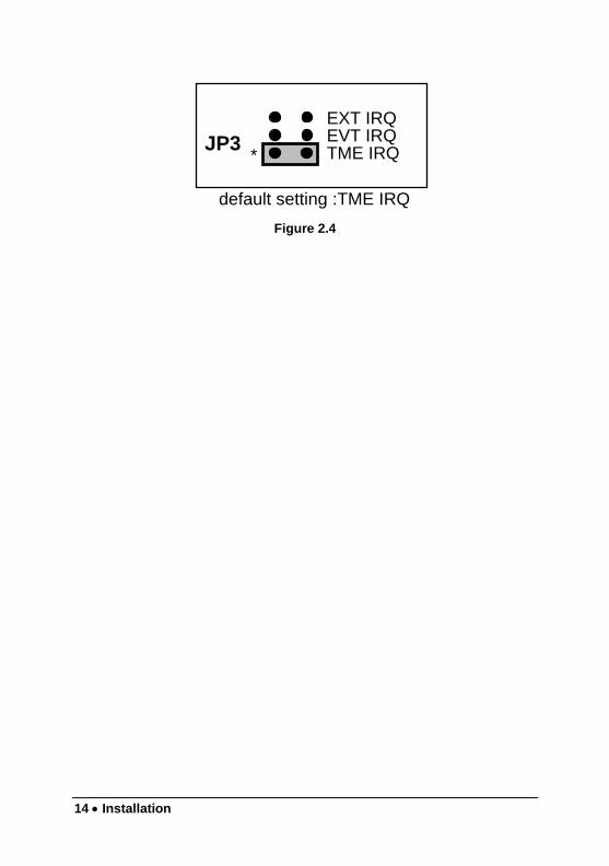
The interrupt trigger source is set by JP3. The default setting is “TME IRQ” and is shown below:
EXT IRQ: External source to trigger interrupt
EVT IRQ: Event counting to trigger interrupt
TME IRQ: Timer Pacer to trigger interrupt
14 • Installation
JP3 *
default setting :TME IRQ
EXT IRQEVT IRQTME IRQ
Figure 2.4
Installation • 15
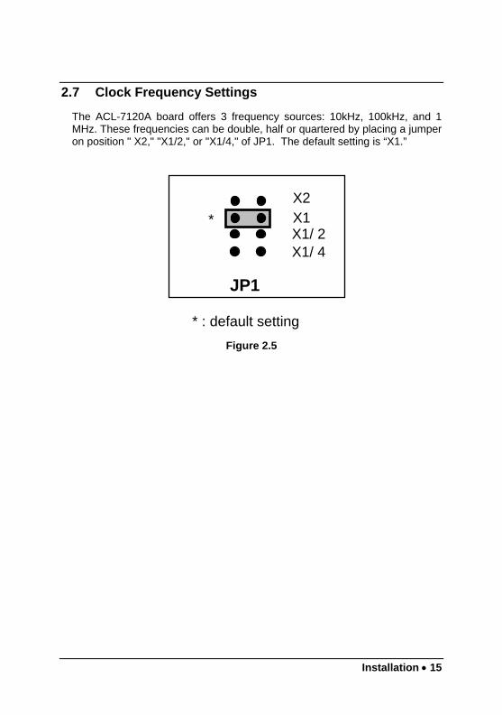
2.7 Clock Frequency Settings
The ACL-7120A board offers 3 frequency sources: 10kHz, 100kHz, and 1 MHz. These frequencies can be double, half or quartered by placing a jumper on position " X2," "X1/2," or "X1/4," of JP1. The default setting is “X1.”
X2X1X1/ 2X1/ 4
JP1
*
* : default setting Figure 2.5
16 • Installation
2.8 ACL-7120A Software Library Installation
The DOS software library is supplied with the ACL-7120A. Function prototypes and useful constants are defined in the header files in the LIB directory. The DOS library software includes a utility program, C language libraries, and demonstration programs to help reduce the programming work. Please refer to the ACLS-DLL1 function reference manual on ADLINK CD. The DOS functions are compatible with ACLS-DLL1 functions except those without a “W” prefix in function names.
To program in a Windows environment, please use ACLS-DLL1 (separate license required).
To install the DOS library software and utilities, please follow the following installation procedures:
1. Insert the ADLINK CD into the CD-ROM drive.
2. Type the following command in a DOS window to change to the card directory (X indicates the CD-ROM drive):
X:\>CD \NuDAQISA\7120
3. Execute the setup batch program to install the software: X:\NuDAQISA\7120>SETUP.
After installation, all files of the ACL-7120A Library & Utility for DOS are stored in the C:\ADLINK\7120\DOS sub-directory.
Signal Connections • 17
3
Signal Connections
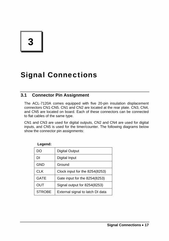
3.1 Connector Pin Assignment
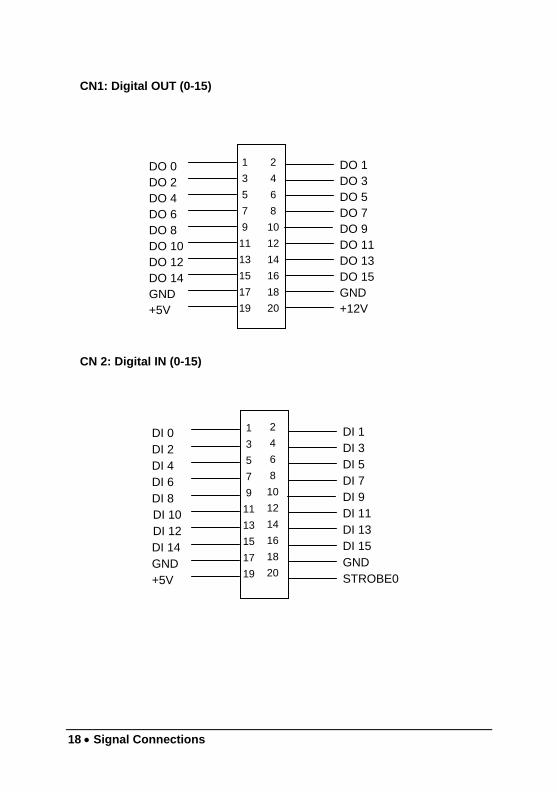
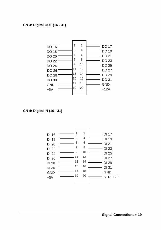
The ACL-7120A comes equipped with five 20-pin insulation displacement connectors CN1-CN5. CN1 and CN2 are located at the rear plate. CN3, CN4, and CN5 are located on board. Each of these connectors can be connected to flat cables of the same type.
CN1 and CN3 are used for digital outputs, CN2 and CN4 are used for digital inputs, and CN5 is used for the timer/counter. The following diagrams below show the connector pin assignments:
Legend:
DO Digital Output
DI Digital Input
GND Ground
CLK Clock input for the 8254(8253)
GATE Gate input for the 8254(8253)
OUT Signal output for 8254(8253)
STROBE External signal to latch DI data
18 • Signal Connections
CN1: Digital OUT (0-15)
CN 2: Digital IN (0-15)
1 3 5 7 9
11 13 15 17 19
DO 0 DO 2 DO 4 DO 6 DO 8 DO 10 DO 12 DO 14 GND +5V
DO 1 DO 3 DO 5 DO 7 DO 9 DO 11 DO 13 DO 15 GND +12V
2 4 6 8
10 12 14 16 18 20
DI 0 DI 2 DI 4 DI 6 DI 8 DI 10 DI 12 DI 14 GND +5V
DI 1 DI 3 DI 5 DI 7 DI 9 DI 11 DI 13 DI 15 GND STROBE0
1 3 5 7 9
11 13 15 17 19
2 4 6 8
10 12 14 16 18 20
Signal Connections • 19
CN 3: Digital OUT (16 - 31)
CN 4: Digital IN (16 - 31)
DO 16 DO 18 DO 20 DO 22 DO 24 DO 26 DO 28 DO 30 GND +5V
DO 17 DO 19 DO 21 DO 23 DO 25 DO 27 DO 29 DO 31 GND +12V
1 3 5 7 9
11 13 15 17 19
2 4 6 8
10 12 14 16 18 20
DI 16 DI 18 DI 20 DI 22 DI 24 DI 26 DI 28 DI 30 GND +5V
DI 17 DI 19 DI 21 DI 23 DI 25 DI 27 DI 29 DI 31 GND STROBE1
1 3 5 7 9
11 13 15 17 19
2 4 6 8
10 12 14 16 18 20
20 • Signal Connections
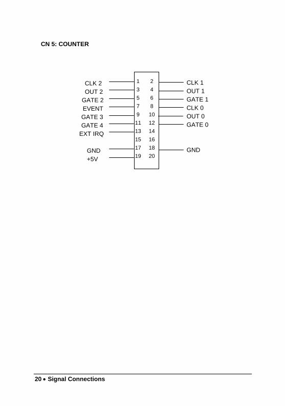
CN 5: COUNTER
CLK 2 OUT 2
GATE 2 EVENT GATE 3 GATE 4
EXT IRQ
GND +5V
CLK 1 OUT 1 GATE 1 CLK 0 OUT 0 GATE 0
GND
1 3 5 7 9
11 13 15 17 19
2 4 6 8
10 12 14 16 18 20
Signal Connections • 21
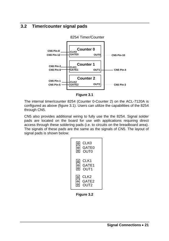
3.2 Timer/counter signal pads
Counter 0
Counter 1
Counter 2
CLK0GATE0 OUT0
CLK1GATE1
CLK2GATE2
OUT1
OUT2
8254 Timer/Counter
CN5 Pin-8CN5 Pin-12 CN5 Pin-10
CN5 Pin-2CN5 Pin-6 CN5 Pin-4
CN5 Pin-3CN5 Pin-1CN5 Pin-5
Figure 3.1
The internal timer/counter 8254 (Counter 0-Counter 2) on the ACL-7120A is configured as above (figure 3.1). Users can utilize the capabilities of the 8254 through CN5.
CN5 also provides additional wiring to fully use the the 8254. Signal solder pads are located on the board for use with applications requiring direct access through these soldering pads (i.e. to circuits on the breadboard area). The signals of these pads are the same as the signals of CN5. The layout of signal pads is shown below.
CLK0GATE0OUT0
CLK1GATE1OUT1
CLK2GATE2OUT2
Figure 3.2
22 • Signal Connections
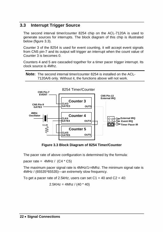
3.3 Interrupt Trigger Source
The second interval timer/counter 8254 chip on the ACL-7120A is used to generate sources for interrupts. The block diagram of this chip is illustrated below (figure 3.3).
Counter 3 of the 8254 is used for event counting, it will accept event signals from CN5 pin-7 and its output will trigger an interrupt when the count value of Counter 3 is becomes 0.
Counters 4 and 5 are cascaded together for a timer pacer trigger interrupt. Its clock source is 4Mhz.
Note: The second internal timer/counter 8254 is installed on the ACL-7120A/6 only. Without it, the functions above will not work.
Counter 3
Counter 4
Counter 5
CLK3GATE3 OUT3
CLK4GATE4
CLK5GATE5
OUT4
OUT5
4MHzOscillator
Vcc Timer Pacer IRQ
8254 Timer/CounterCN5 Pin-7 EVENT
CN5 Pin-9 GATE3
Event IRQExternal IRQ
CN5 Pin-13External IRQ
Figure 3.3 Block Diagram of 8254 Timer/Counter
The pacer rate of above configuration is determined by the formula:
pacer rate = 4MHz / (C4 * C5)
The maximum pacer signal rate is 4MHz/1=4Mhz. The minimum signal rate is 4MHz / (65535*65535)—an extremely slow frequency.
To get a pacer rate of 2.5kHz, users can set C1 = 40 and C2 = 40:
2.5KHz = 4Mhz / (40 * 40)
Signal Connections • 23
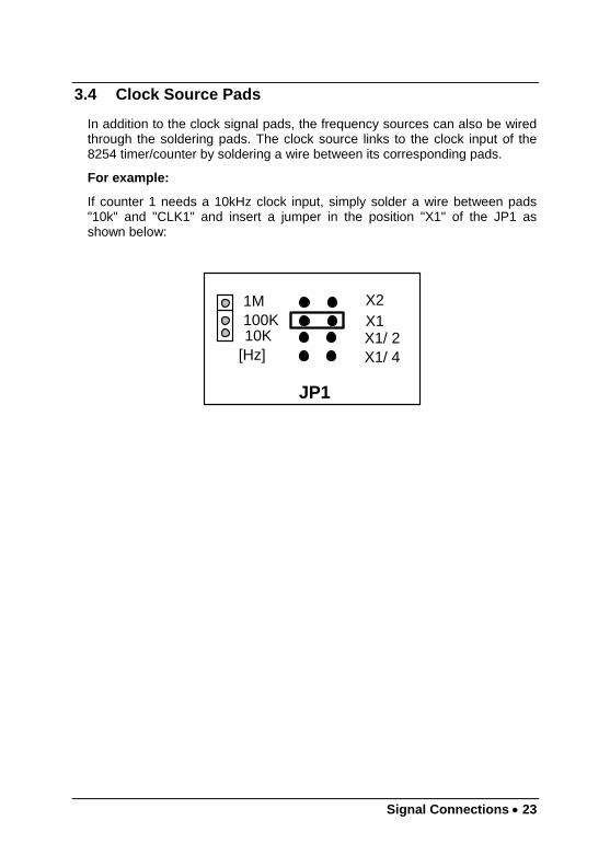
3.4 Clock Source Pads
In addition to the clock signal pads, the frequency sources can also be wired through the soldering pads. The clock source links to the clock input of the 8254 timer/counter by soldering a wire between its corresponding pads.
For example:
If counter 1 needs a 10kHz clock input, simply solder a wire between pads "10k" and "CLK1" and insert a jumper in the position "X1" of the JP1 as shown below:
X2X1X1/ 2X1/ 4
JP1
1M100K10K
[Hz]
24 • Signal Connections
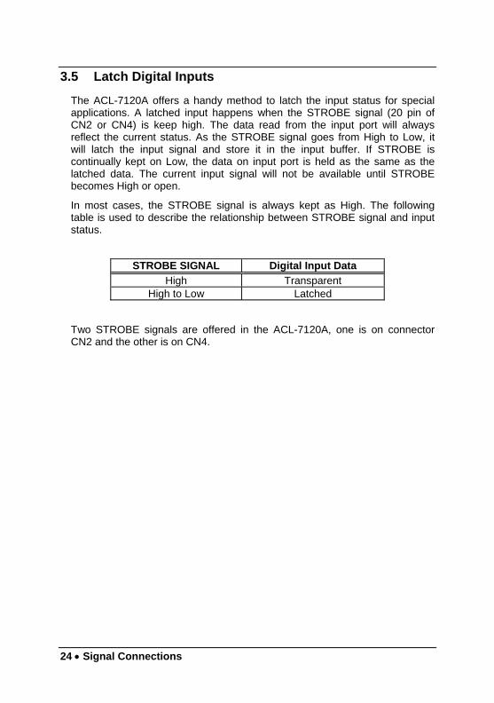
3.5 Latch Digital Inputs
The ACL-7120A offers a handy method to latch the input status for special applications. A latched input happens when the STROBE signal (20 pin of CN2 or CN4) is keep high. The data read from the input port will always reflect the current status. As the STROBE signal goes from High to Low, it will latch the input signal and store it in the input buffer. If STROBE is continually kept on Low, the data on input port is held as the same as the latched data. The current input signal will not be available until STROBE becomes High or open.
In most cases, the STROBE signal is always kept as High. The following table is used to describe the relationship between STROBE signal and input status.
STROBE SIGNAL Digital Input Data
High Transparent High to Low Latched
Two STROBE signals are offered in the ACL-7120A, one is on connector CN2 and the other is on CN4.
Programming • 25
4
Programming
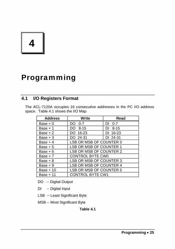
4.1 I/O Registers Format
The ACL-7120A occupies 16 consecutive addresses in the PC I/O address space. Table 4.1 shows the I/O Map
Address Write Read Base + 0 DO 0-7 DI 0-7 Base + 1 DO 8-15 DI 8-15 Base + 2 DO 16-23 DI 16-23 Base + 3 DO 24-31 DI 24-31 Base + 4 LSB OR MSB OF COUNTER 0 Base + 5 LSB OR MSB OF COUNTER 1 Base + 6 LSB OR MSB OF COUNTER 2 Base + 7 CONTROL BYTE CW0 Base + 8 LSB OR MSB OF COUNTER 3 Base + 9 LSB OR MSB OF COUNTER 4 Base + 10 LSB OR MSB OF COUNTER 5 Base + 11 CONTROL BYTE CW1
DO -- Digital Output
DI -- Digital Input
LSB -- Least Significant Byte
MSB -- Most Significant Byte
Table 4.1
26 • Programming
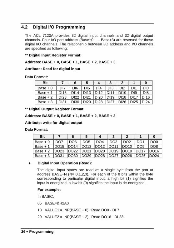
4.2 Digital I/O Programming
The ACL 7120A provides 32 digital input channels and 32 digital output channels. Four I/O port address (Base+0, ..., Base+3) are reserved for these digital I/O channels. The relationship between I/O address and I/O channels are specified as following:
** Digital Input Register Format:
Address: BASE + 0, BASE + 1, BASE + 2, BASE + 3
Attribute: Read for digital input
Data Format: Bit 7 6 5 4 3 2 1 0
Base + 0 DI7 DI6 DI5 DI4 DI3 DI2 DI1 DI0 Base + 1 DI15 DI14 DI13 DI12 DI11 DI10 DI9 DI8 Base + 2 DI23 DI22 DI21 DI20 DI19 DI18 DI17 DI16 Base + 3 DI31 DI30 DI29 DI28 DI27 DI26 DI25 DI24
** Digital Output Register Format:
Address: BASE + 0, BASE + 1, BASE + 2, BASE + 3
Attribute: write for digital output
Data Format:
Bit 7 6 5 4 3 2 1 0 Base + 0 DO7 DO6 DO5 DO4 DO3 DO2 DO1 DO0 Base + 1 DO15 DO14 DO13 DO12 DO11 DO10 DO9 DO8 Base + 2 DO23 DO22 DO21 DO20 DO19 DO18 DO17 DO16 Base + 3 DO31 DO30 DO29 DO28 DO27 DO26 DO25 DO24
♦ Digital Input Operation (Read):
The digital input states are read as a single byte from the port at address BASE+N (N= 0,1,2,3). For each of the 8 bits within the byte corresponding to particular digital input, a high bit (1) signifies the input is energized, a low bit (0) signifies the input is de-energized.
For example:
In BASIC,
05 BASE=&H2A0
10 VALUE1 = INP(BASE + 0) ‘Read DO0 - DI 7
20 VALUE2 = INP(BASE + 2) ‘Read DO16 - DI 23
Programming • 27
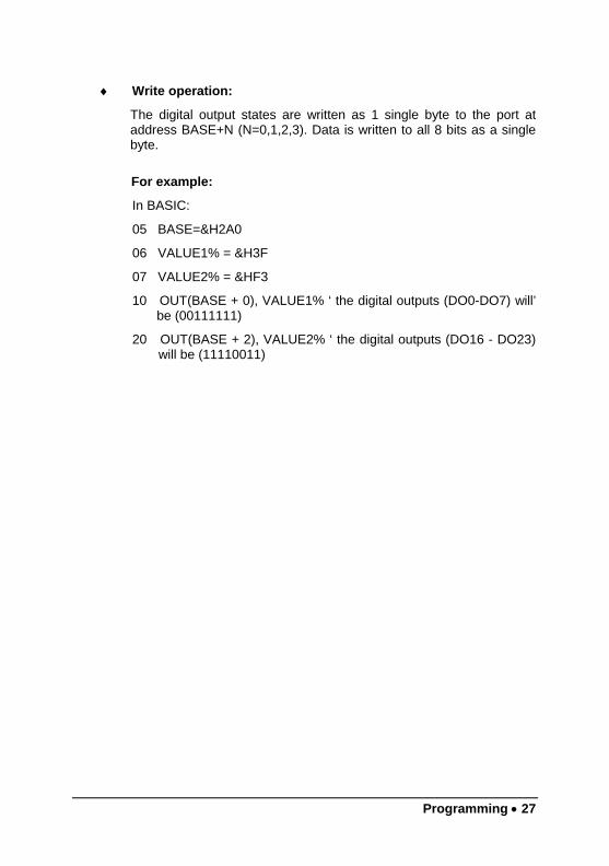
♦ Write operation:
The digital output states are written as 1 single byte to the port at address BASE+N (N=0,1,2,3). Data is written to all 8 bits as a single byte.
For example:
In BASIC:
05 BASE=&H2A0
06 VALUE1% = &H3F
07 VALUE2% = &HF3
10 OUT(BASE + 0), VALUE1% ‘ the digital outputs (DO0-DO7) will’ be (00111111)
20 OUT(BASE + 2), VALUE2% ‘ the digital outputs (DO16 - DO23) will be (11110011)
28 • Programming
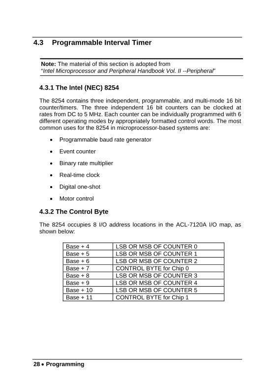
4.3 Programmable Interval Timer
Note: The material of this section is adopted from “Intel Microprocessor and Peripheral Handbook Vol. II --Peripheral”
4.3.1 The Intel (NEC) 8254
The 8254 contains three independent, programmable, and multi-mode 16 bit counter/timers. The three independent 16 bit counters can be clocked at rates from DC to 5 MHz. Each counter can be individually programmed with 6 different operating modes by appropriately formatted control words. The most common uses for the 8254 in microprocessor-based systems are:
• Programmable baud rate generator
• Event counter
• Binary rate multiplier
• Real-time clock
• Digital one-shot
• Motor control
4.3.2 The Control Byte
The 8254 occupies 8 I/O address locations in the ACL-7120A I/O map, as shown below:
Base + 4 LSB OR MSB OF COUNTER 0 Base + 5 LSB OR MSB OF COUNTER 1 Base + 6 LSB OR MSB OF COUNTER 2 Base + 7 CONTROL BYTE for Chip 0 Base + 8 LSB OR MSB OF COUNTER 3 Base + 9 LSB OR MSB OF COUNTER 4 Base + 10 LSB OR MSB OF COUNTER 5 Base + 11 CONTROL BYTE for Chip 1
Programming • 29
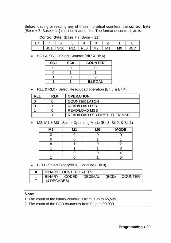
Before loading or reading any of these individual counters, the control byte (Base + 7, Base + 11) must be loaded first. The format of control byte is:
Control Byte: (Base + 7, Base + 11) Bit 7 6 5 4 3 2 1 0
SC1 SC0 RL1 RL0 M2 M1 M0 BCD
• SC1 & SC1 - Select Counter (Bit7 & Bit 6)
SC1 SC0 COUNTER 0 0 0 0 1 1 1 0 2 1 1 ILLEGAL
• RL1 & RL0 - Select Read/Load operation (Bit 5 & Bit 4)
RL1 RL0 OPERATION 0 0 COUNTER LATCH 0 1 READ/LOAD LSB 1 0 READ/LOAD MSB 1 1 READ/LOAD LSB FIRST, THEN MSB
• M2, M1 & M0 - Select Operating Mode (Bit 3, Bit 2, & Bit 1)
M2 M1 M0 MODE 0 0 0 0 0 0 1 1 x 1 0 2 x 1 1 3 1 0 0 4 1 0 1 5
• BCD - Select Binary/BCD Counting ( Bit 0)
0 BINARY COUNTER 16-BITS
1 BINARY CODED DECIMAL (BCD) COUNTER (4 DECADES)
Note: 1. The count of the binary counter is from 0 up to 65,535. 2. The count of the BCD counter is from 0 up to 99,999.
30 • Programming
4.3.3 Mode definition
There are six different selectable operating modes in the 8254:
Mode 0: Interrupt on terminal count
The output will be initially low after the mode set operation. After the count is loaded into the selected count register, the output will remain low and the counter will begin counting. When terminal count is reached, the output will go high and remain high until the selected count register is reloaded with a mode or a new count is loaded. The counter continues to decrement after terminal count has been reached.
Rewriting a counter register during counting is done by:
(1) Write 1st byte stops the current counting.
(2) Write 2nd byte starts the new count.
Mode 1: Programmable One-Shot
The output will go low on the count following the rising edge of the gate input. The output will go high on the terminal count. If a new count value is loaded while the output is low it will not affect the duration of the one-shot pulse until the succeeding trigger. The current count can be read at anytime without affecting the one-shot pulse.
The one-shot is re-triggerable, hence the output will remain low for the full count after any rising edge of the gate input.
Mode 2: Rate Generator
A Divide by N counter. The output will be low for one period of the input clock. The period from one output pulse to the next equals the number of input counts in the count register. If the count register is reloaded between output pulses the present period will not be affected, but the subsequent period will reflect the new value.
The gate input, when low, will force the output high. When the gate input goes high, the counter will start form the initial count. Thus, the gate input can be synchronized by software.
When this mode is set, the output will remain high until after the count register is loaded. The output can also be synchronized by software.
Programming • 31
Mode 3: Square Wave Rate Generator.
Similar to Mode 2 except that the output will remain high until one half of the count has been completed (or for even counts) and go low for the other half of the count. This is accomplished by decrementing the counter by two on the falling edge of each clock pulse. When the counter reaches terminal count, the state of the output is changed and the counter is reloaded with the full count and the whole process is repeated.
If the count is odd and the output is high, the first clock pulse (after the count is loaded) decrements the count by 1. Subsequent clock pulses decrement the clock by 2. After time-out, the output goes low and the full count is reloaded. The first clock pulse (following the reload) decrements the counter by 3. Subsequent clock pulses decrement the count by 2 until time-out. Then the whole process is repeated. In this way, if the count is odd, the output will be high for (N + 1)/2 counts and low for (N - 1)/2 counts.
In Modes 2 and 3, if a CLK source other then the system clock is used, GATE should be pulsed immediately following Way Rate of a new count value.
Mode 4: Software Triggered Strobe.
After the mode is set, the output will be high. When the count is loaded, the counter will begin counting. On the terminal count, the output will go low for one input clock period, then high again.
If the count register is reloaded during counting, the new count will be loaded on the next CLK pulse. The count will be inhibited while the GATE input is low.
Mode 5: Hardware Triggered Strobe.
The counter will start counting after the rising edge of the trigger input and will go low for one clock period when the terminal count is reached. The counter is re-triggerable. The output will not go low until the full count after the rising edge of any trigger.

Warranty Policy• 33
Warranty Policy
Thank you for choosing ADLINK. To understand your rights and enjoy all the after-sales services we offer, please read the following carefully:
1. Before using ADLINK’s products please read the user manual and follow the instructions exactly.
2. When sending in damaged products for repair, please attach an RMA application form.
3. All ADLINK products come with a two-year guarantee, repaired free of charge.
• The warranty period starts from the product’s shipment date from ADLINK’s factory.
• Peripherals and third-party products not manufactured by ADLINK will be covered by the original manufacturers’ warranty.
• End users requiring maintenance services should contact their local dealers. Local warranty conditions will depend on local dealers.
4. This warranty will not cover repair costs due to:
a. Damage caused by not following instructions.
b. Damage caused by carelessness on the users’ part during product transportation.
c. Damage caused by fire, earthquakes, floods, lightening, pollution, other acts of God, and/or incorrect usage of voltage transformers.
d. Damage caused by unsuitable storage environments (i.e. high temperatures, high humidity, or volatile chemicals.
e. Damage caused by leakage of battery fluid.
f. Damage from improper repair by unauthorized technicians.

34 • Warranty Policy
g. Products with altered and/or damaged serial numbers.
h. Other categories not protected under our guarantees.
5. Customers are responsible for shipping costs to transport damaged products to our company or sales office.
6. To ensure the speed and quality of product repair, please download a RMA application form from our company website: www.adlinktech.com. Damaged products with attached RMA forms receive priority.
For further questions, please contact our FAE staff.
ADLINK: [email protected]