Embed Size (px)
Citation preview
Digital Integrated Circuits © Prentice Hall 1995Timing
ISSUES IN TIMING
Digital Integrated Circuits © Prentice Hall 1995Timing
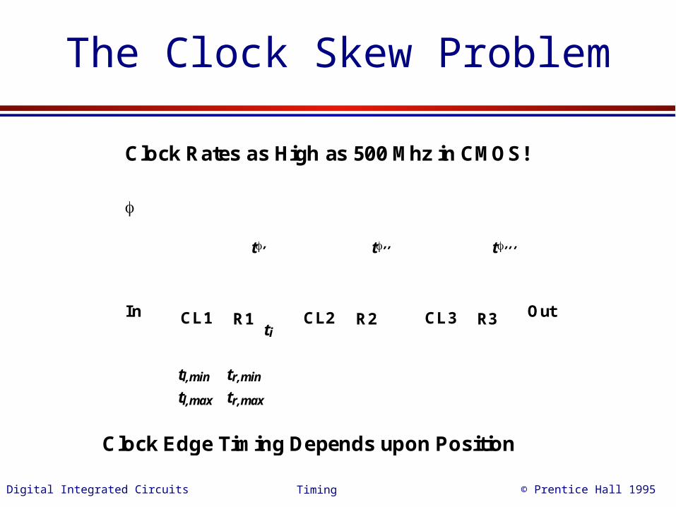
The Clock Skew Problem
CL1 R1 CL2 R2 CL3 R3In Out
t’ t’’ t’’’
tl,mintl,max
tr,mintr,max
ti
Clock Edge Timing Depends upon Position
Clock Rates as High as 500 Mhz in CMOS!
Digital Integrated Circuits © Prentice Hall 1995Timing
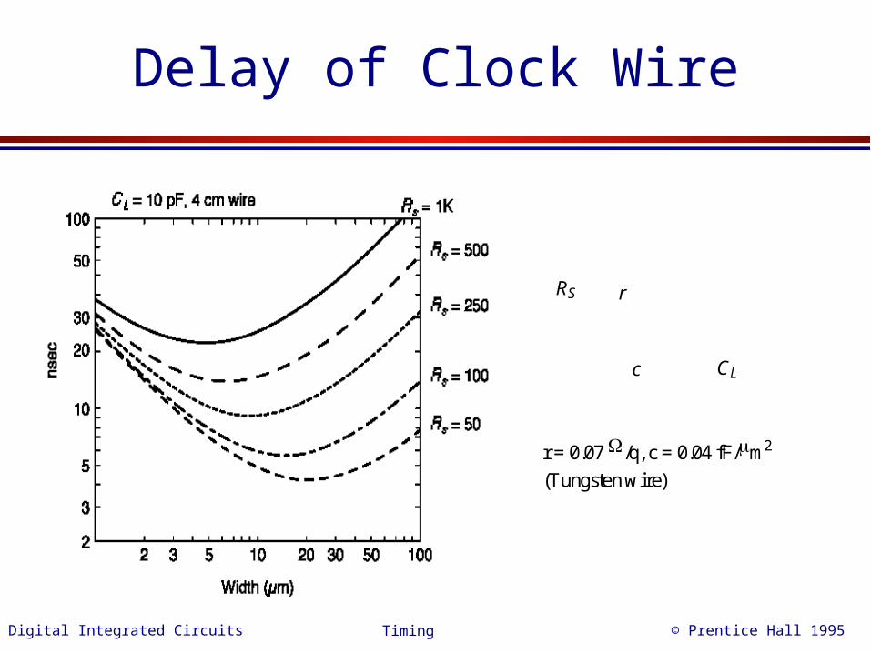
Delay of Clock Wire
CL
r
c
RS
r = 0.07 /q, c = 0.04 fF/m2
(Tungsten wire)
Digital Integrated Circuits © Prentice Hall 1995Timing
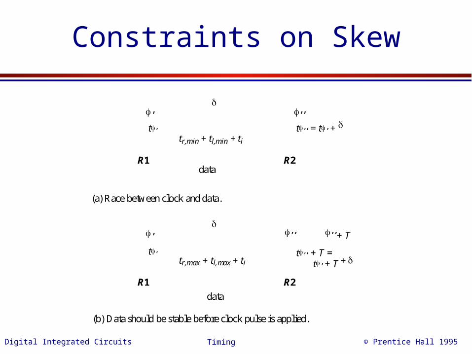
Constraints on Skew
R1 R2
’ ’’
tr,min + tl,min + ti
(a) Race between clock and data.
R1 R2
’ ’’+ T
tr,max + tl,max + ti
(b) Data should be stable before clock pulse is applied.
t’ t’’ = t’ +
t’ t’’ + T =
data
data
’’
t’ + T
Digital Integrated Circuits © Prentice Hall 1995Timing
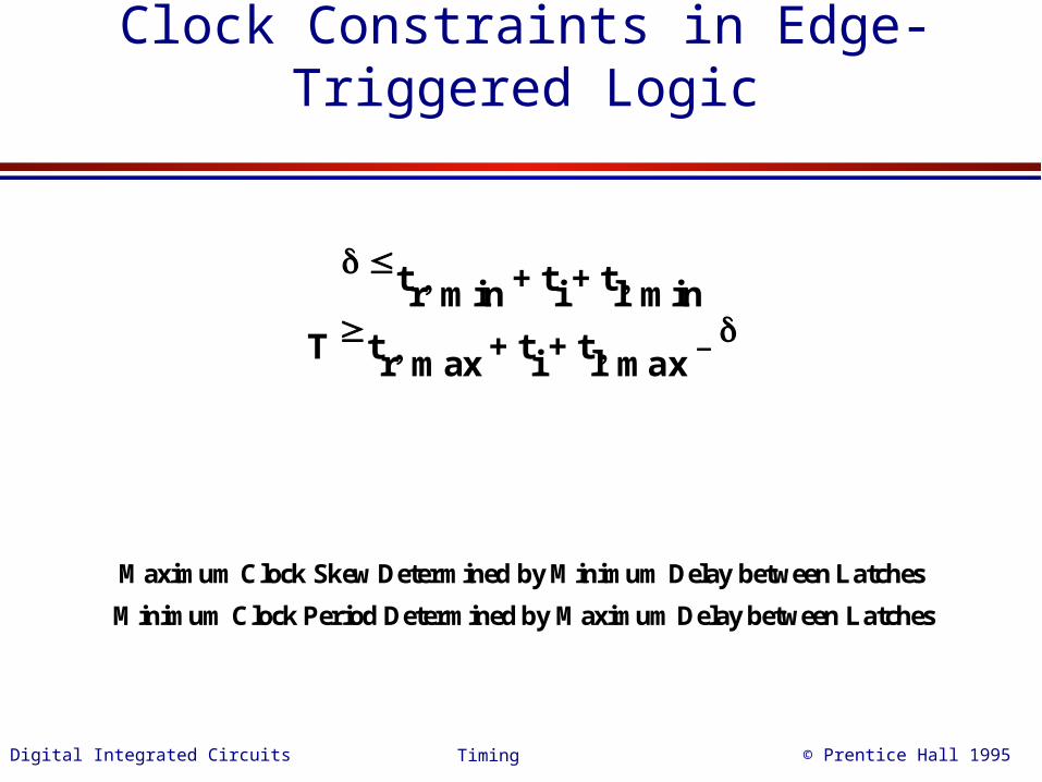
Clock Constraints in Edge-Triggered Logic
tr min ti tl min+ +
T tr max ti tl max –+ +
Maximum Clock Skew Determined by Minimum Delay between Latches
Minimum Clock Period Determined by Maximum Delay between Latches
Digital Integrated Circuits © Prentice Hall 1995Timing
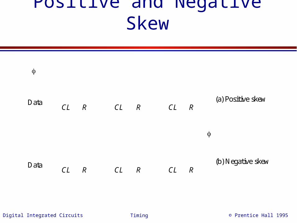
Positive and Negative Skew
R CL R CL RData
CL
R CL R CL RData
CL
(a) Positive skew
(b) Negative skew
Digital Integrated Circuits © Prentice Hall 1995Timing
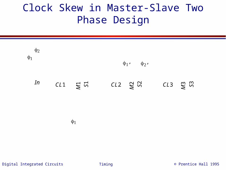
Clock Skew in Master-Slave Two Phase Design
M1CL1 CL2 CL3In
S1 S2 S3M2
M3
’’
Digital Integrated Circuits © Prentice Hall 1995Timing
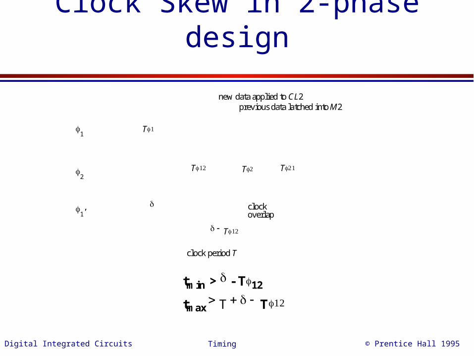
Clock Skew in 2-phase design
clock period T
T
T T T
T
1
2
1’clockoverlap
new data applied to CL2previous data latched into M2
tmin > - T12
tmax T T
Digital Integrated Circuits © Prentice Hall 1995Timing
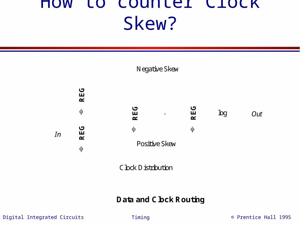
How to counter Clock Skew?
RE
G
RE
G
RE
G
.
RE
G
log Out
In
Clock Distribution
Positive Skew
Negative Skew
Data and Clock Routing
Digital Integrated Circuits © Prentice Hall 1995Timing
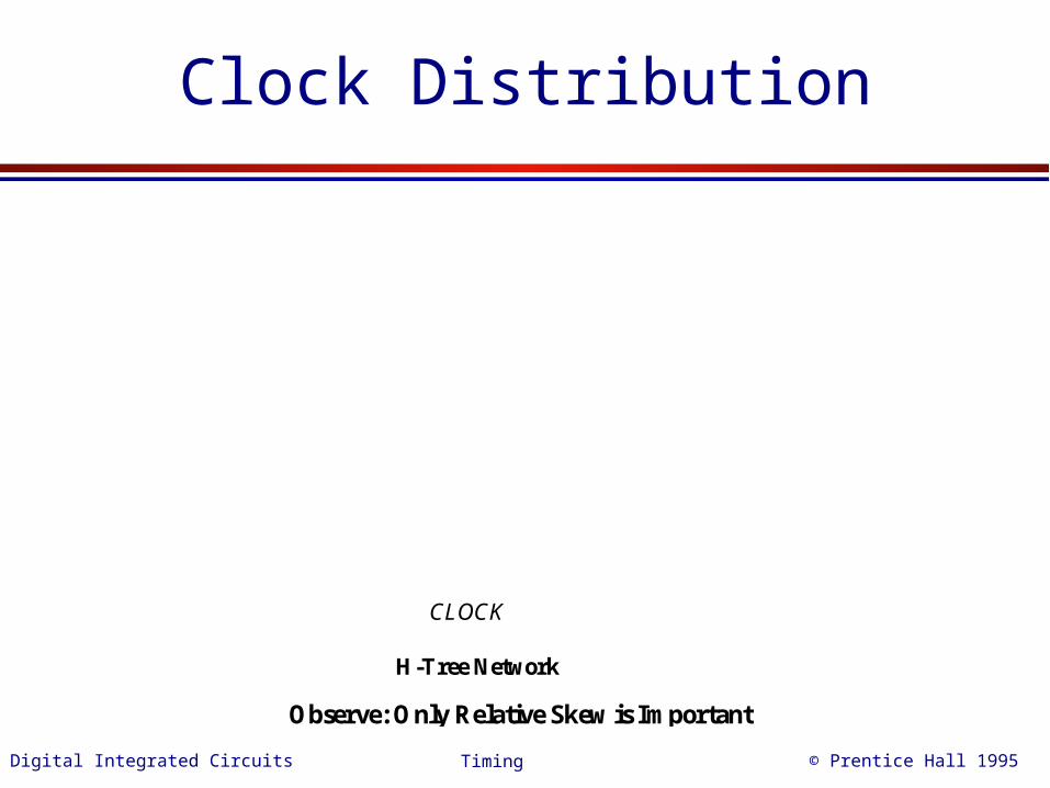
Clock Distribution
CLOCK
H-Tree Network
Observe: Only Relative Skew is Important
Digital Integrated Circuits © Prentice Hall 1995Timing
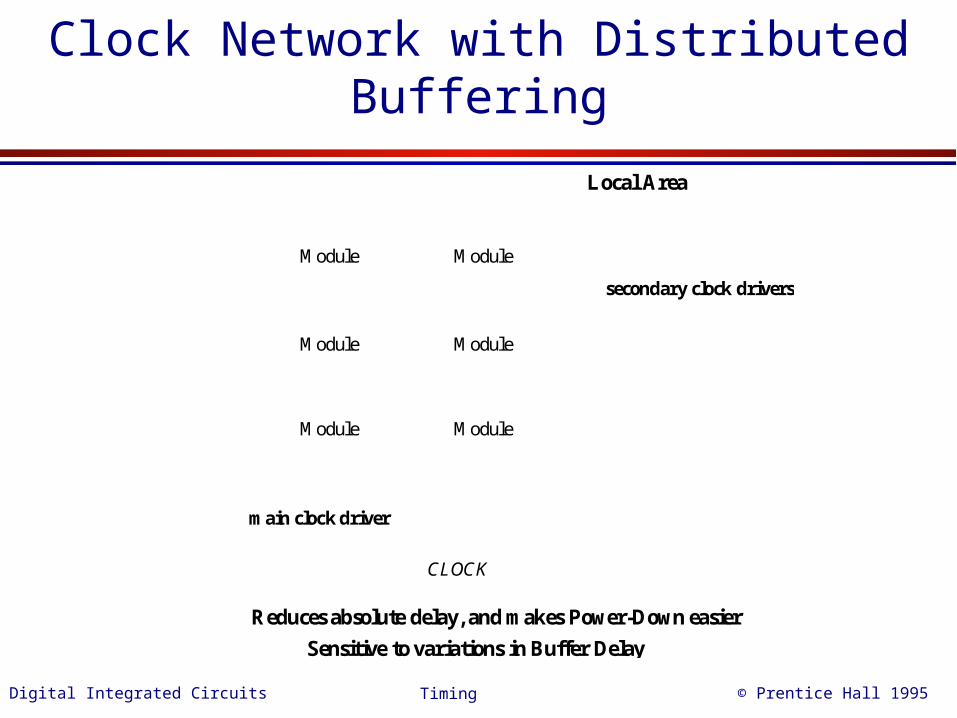
Clock Network with Distributed Buffering
Module
Module
Module
Module
Module
Module
CLOCK
main clock driver
secondary clock drivers
Reduces absolute delay, and makes Power-Down easier
Sensitive to variations in Buffer Delay
Local Area
Digital Integrated Circuits © Prentice Hall 1995Timing
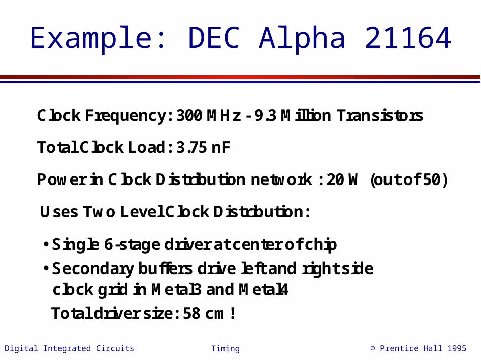
Example: DEC Alpha 21164
Clock Frequency: 300 MHz - 9.3 Million Transistors
Total Clock Load: 3.75 nF
Power in Clock Distribution network : 20 W (out of 50)
Uses Two Level Clock Distribution:
• Single 6-stage driver at center of chip
• Secondary buffers drive left and right sideclock grid in Metal3 and Metal4
Total driver size: 58 cm!
Digital Integrated Circuits © Prentice Hall 1995Timing
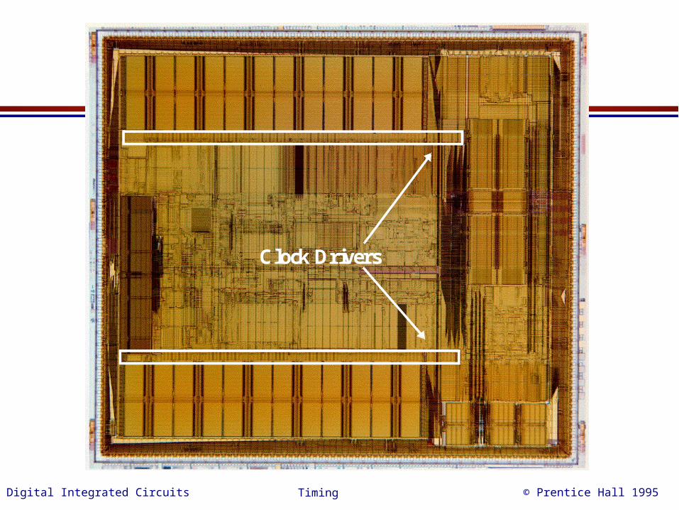
Clock Drivers
Digital Integrated Circuits © Prentice Hall 1995Timing
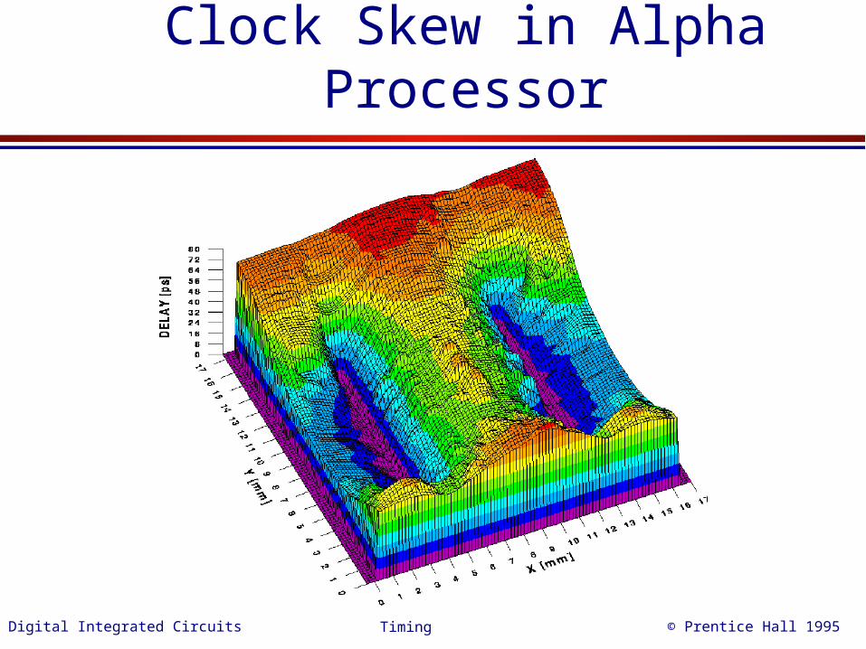
Clock Skew in Alpha Processor
Digital Integrated Circuits © Prentice Hall 1995Timing
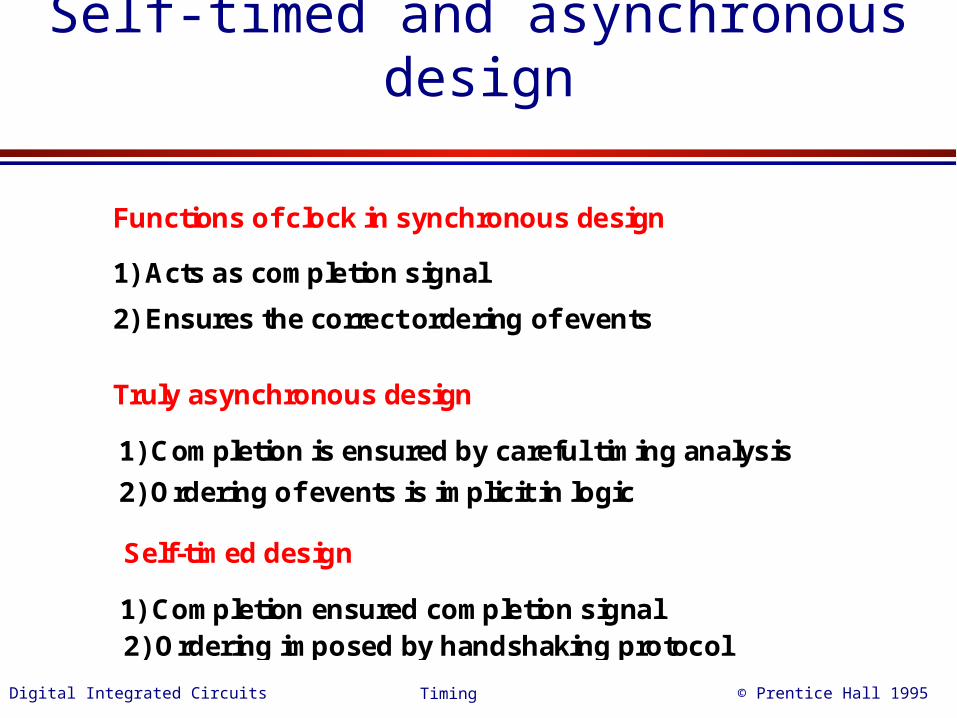
Self-timed and asynchronous design
Functions of clock in synchronous design
1) Acts as completion signal
2) Ensures the correct ordering of events
Truly asynchronous design
2) Ordering of events is implicit in logic
1) Completion is ensured by careful timing analysis
Self-timed design
1) Completion ensured completion signal2) Ordering imposed by handshaking protocol
Digital Integrated Circuits © Prentice Hall 1995Timing
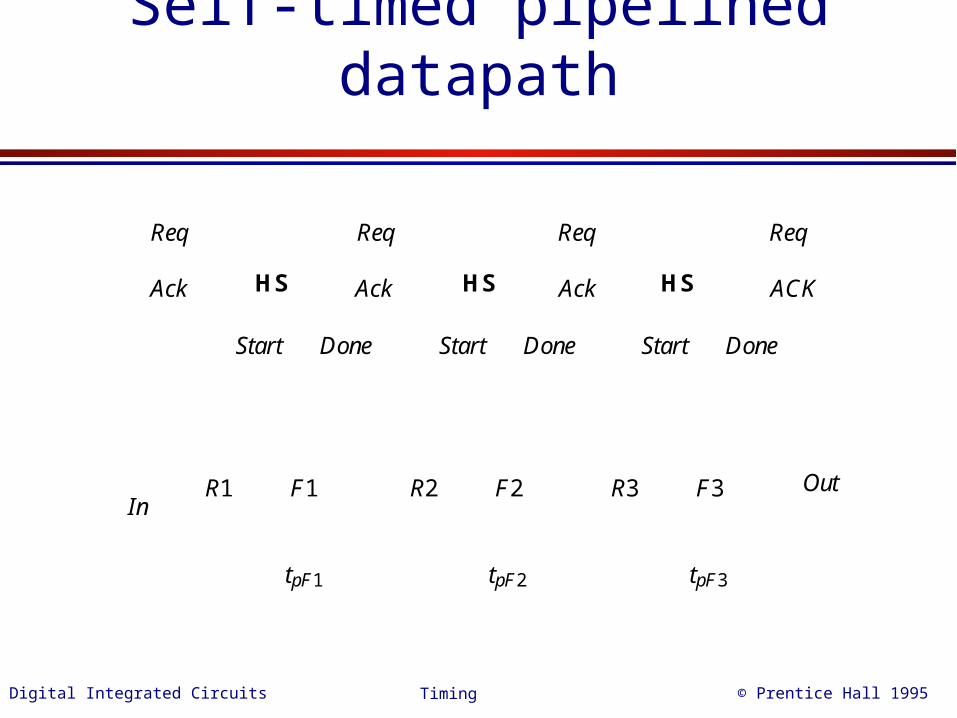
Self-timed pipelined datapath
R2 OutF2In
tpF2
Start Done
R1 F1
tpF1
Start Done
R3 F3
tpF3
Start Done
Req Req Req Req
Ack Ack Ack ACKHS HS HS
Digital Integrated Circuits © Prentice Hall 1995Timing
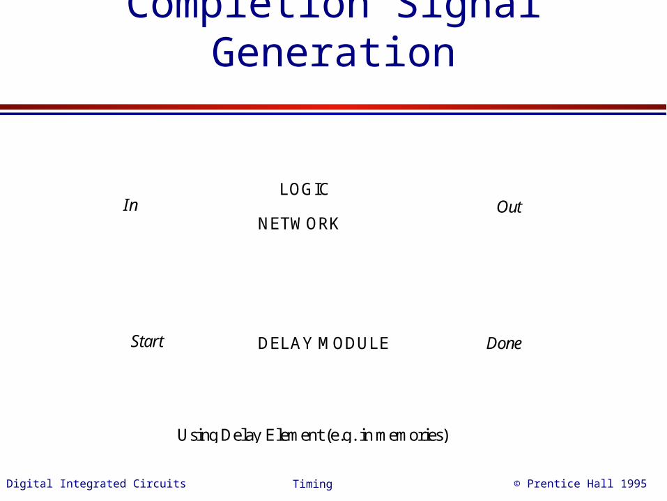
Completion Signal Generation
LOGIC
NETWORK
DELAY MODULE
In Out
Start Done
Using Delay Element (e.g. in memories)
Digital Integrated Circuits © Prentice Hall 1995Timing
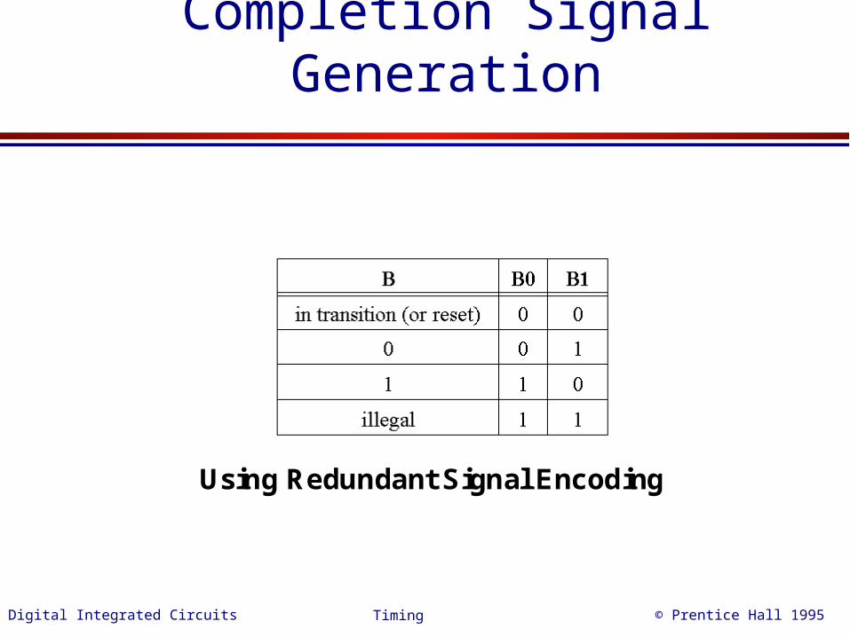
Completion Signal Generation
Using Redundant Signal Encoding
Digital Integrated Circuits © Prentice Hall 1995Timing
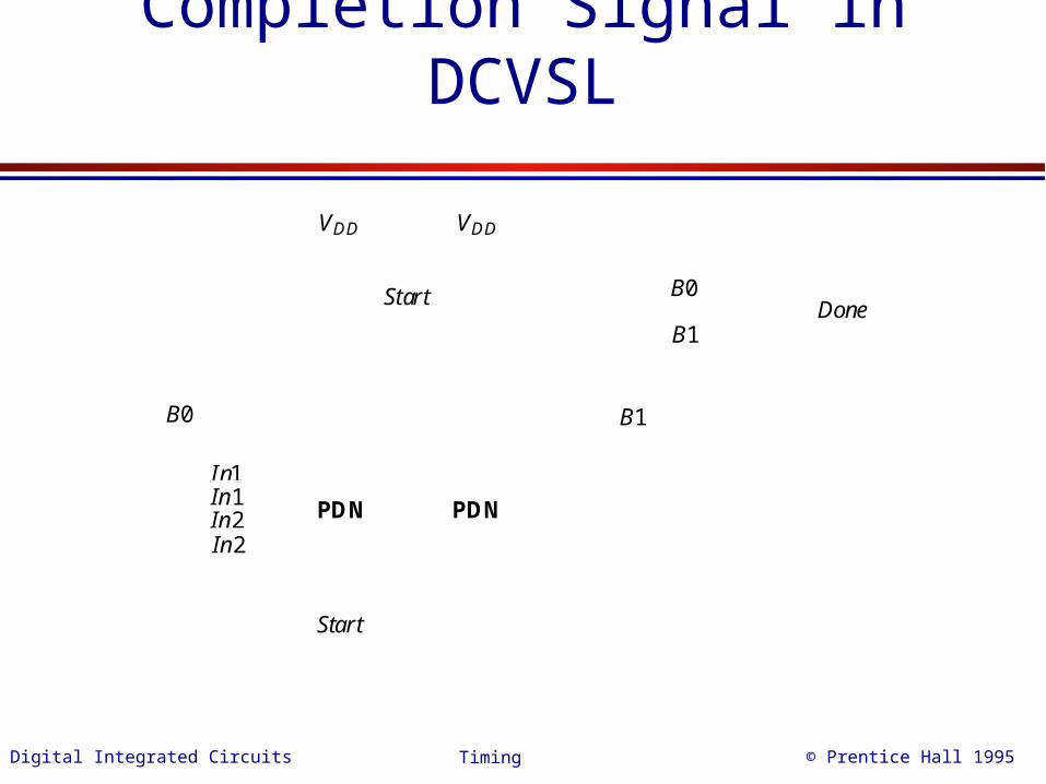
Completion Signal in DCVSL
PDN
B0
PDN
In1In1In2In2
B1
Start
Start
VDD VDD
DoneB0
B1
Digital Integrated Circuits © Prentice Hall 1995Timing
Self-timed Adder
P0
C0
P1
G0
P2
G1
P3
G2 G3
VDD
Start
Start
P0
C0
P1
K0
P2
K1
P3
K2 K3
VDD
Start
Start
C0 C1 C2 C3 C4 C4
C4C0 C1 C2 C3 C4
VDD
Start
C4
C3
C2
C1
C4
C3
C2
C1
Start Done
(a) Differential carry generation
(b) Completion signal
Digital Integrated Circuits © Prentice Hall 1995Timing
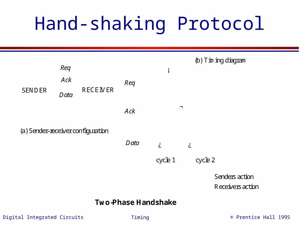
Hand-shaking Protocol
Req
Ack
DataSENDER RECEIVER
Senders action
Receivers action
Req
Ack
Data
cycle 1 cycle 2
¿ ¿
¡
¬
(a) Sender-receiver configuration
(b) Timing diagram
Two-Phase Handshake
Digital Integrated Circuits © Prentice Hall 1995Timing
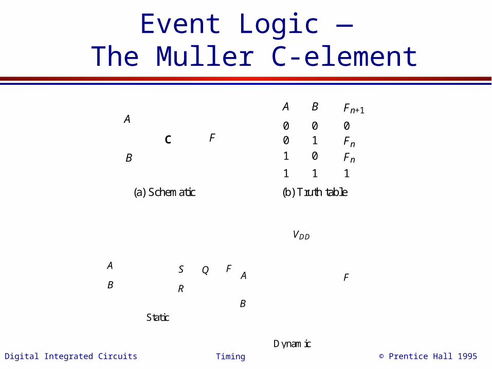
Event Logic — The Muller C-element
C
A
B
F
A B Fn+1
00
1
1
01
0
1
0Fn
Fn
1
(a) Schematic (b) Truth table
VDD
FA
B
QS
R
A
B
F
Static
Dynamic
Digital Integrated Circuits © Prentice Hall 1995Timing
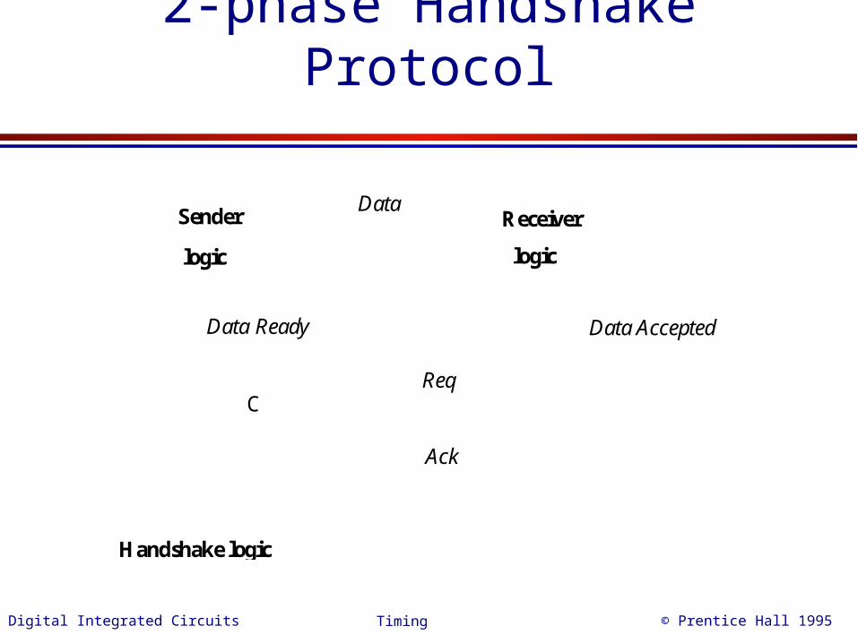
2-phase Handshake Protocol
C
Sender
logic
Receiver
logic
Data
Data Ready
Req
Ack
Data Accepted
Handshake logic
Digital Integrated Circuits © Prentice Hall 1995Timing
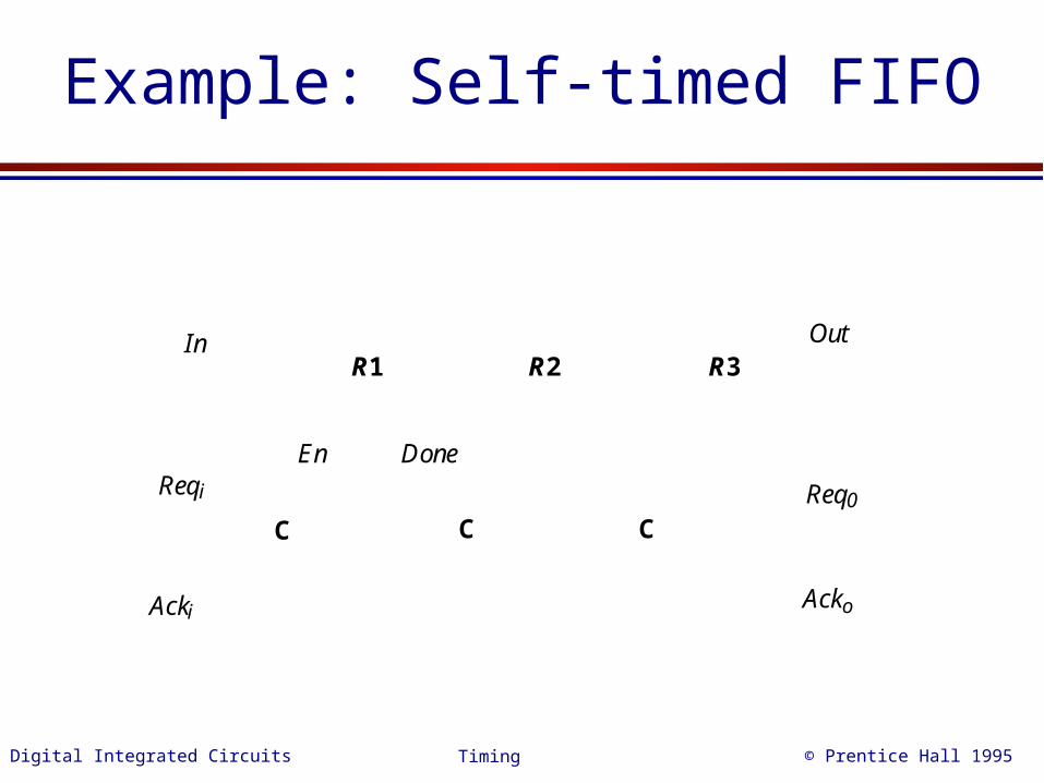
Example: Self-timed FIFO
C C
R1In Out
En
Acki
Reqi
R2 R3
CReq0
Acko
Done
Digital Integrated Circuits © Prentice Hall 1995Timing
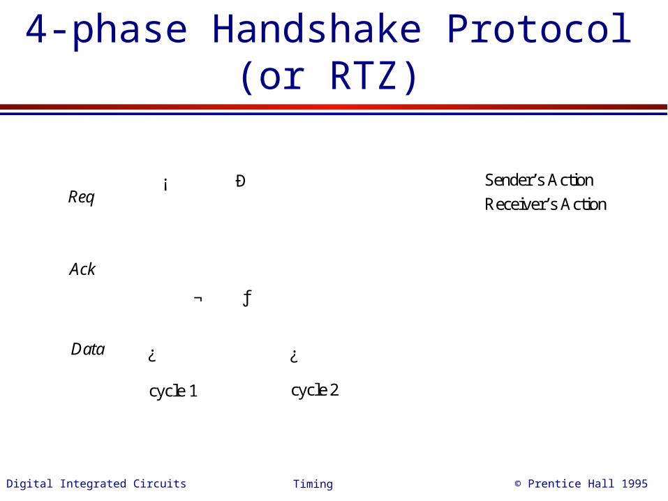
4-phase Handshake Protocol (or RTZ)
Sender’s Action
Receiver’s ActionReq
Ack
Data
cycle 1 cycle 2
¿ ¿
¡
¬
Ð
ƒ
Digital Integrated Circuits © Prentice Hall 1995Timing
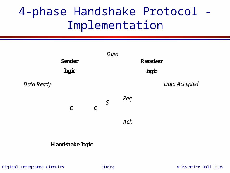
4-phase Handshake Protocol -Implementation
C
Sender
logic
Receiver
logic
Data
Data Ready
Req
Ack
Data Accepted
C
Handshake logic
S
Digital Integrated Circuits © Prentice Hall 1995Timing
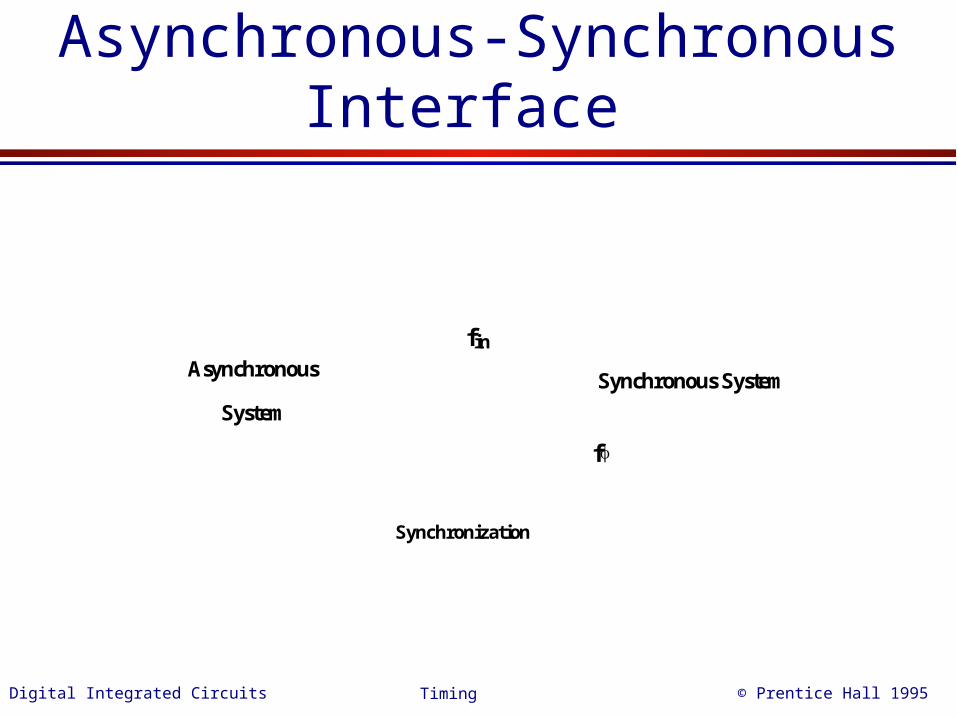
Asynchronous-Synchronous Interface
Asynchronous
System
Synchronous System
f
fin
Synchronization
Digital Integrated Circuits © Prentice Hall 1995Timing
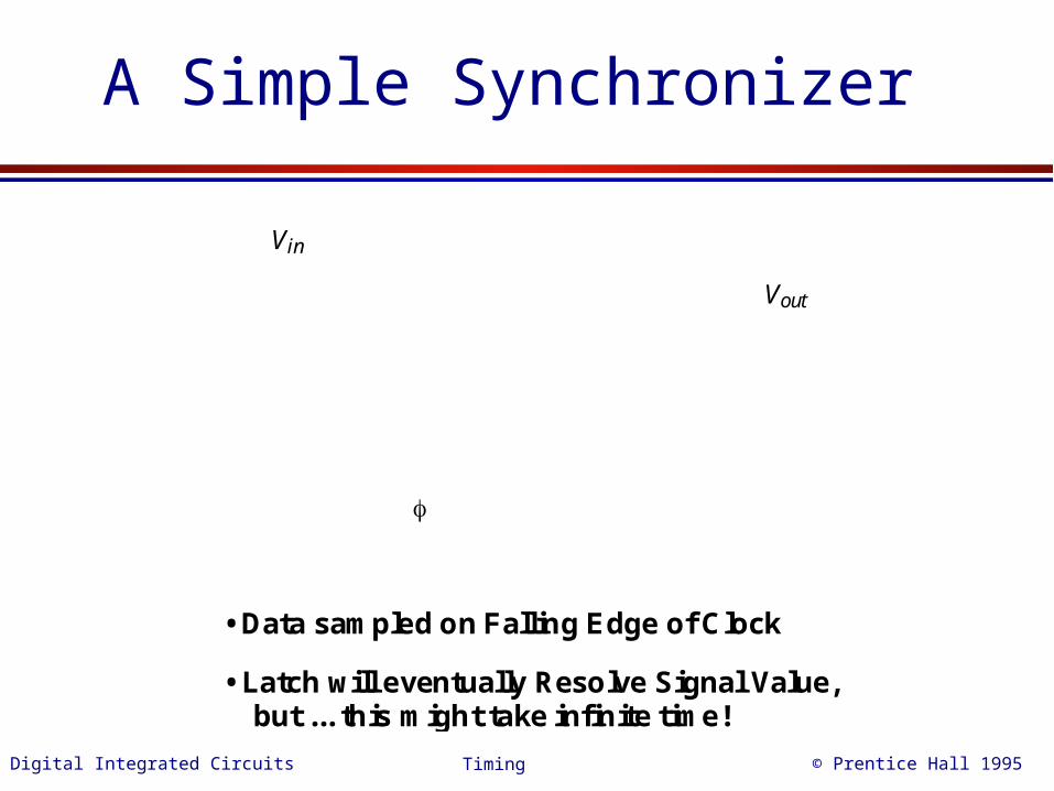
A Simple Synchronizer
Vin
Vout
• Data sampled on Falling Edge of Clock
• Latch will eventually Resolve Signal Value,but ... this might take infinite time!
Digital Integrated Circuits © Prentice Hall 1995Timing
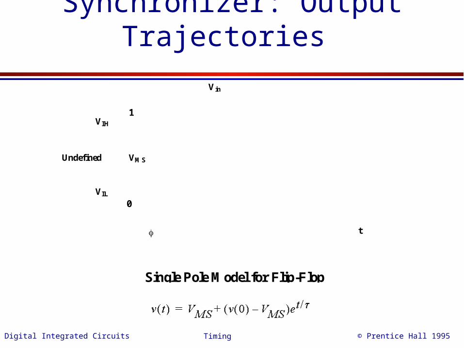
Synchronizer: Output Trajectories
Vin
VIH
VIL
Undefined VMS
t
1
0
Single Pole Model for Flip-Flop
Digital Integrated Circuits © Prentice Hall 1995Timing
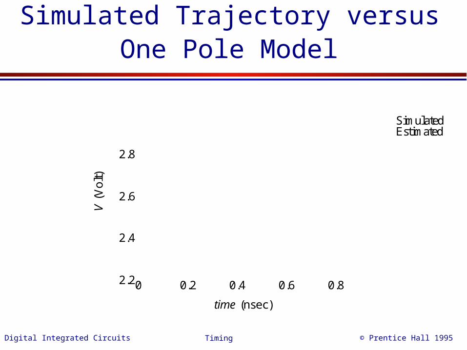
Simulated Trajectory versus One Pole Model
SimulatedEstimated
0 0.2 0.4 0.6 0.8
time (nsec)
2.2
2.4
2.6
2.8
V (
Vol
t)
Digital Integrated Circuits © Prentice Hall 1995Timing
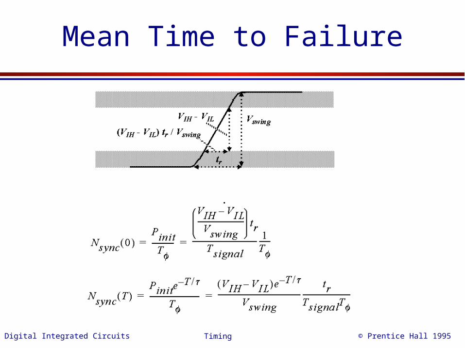
Mean Time to Failure
Digital Integrated Circuits © Prentice Hall 1995Timing
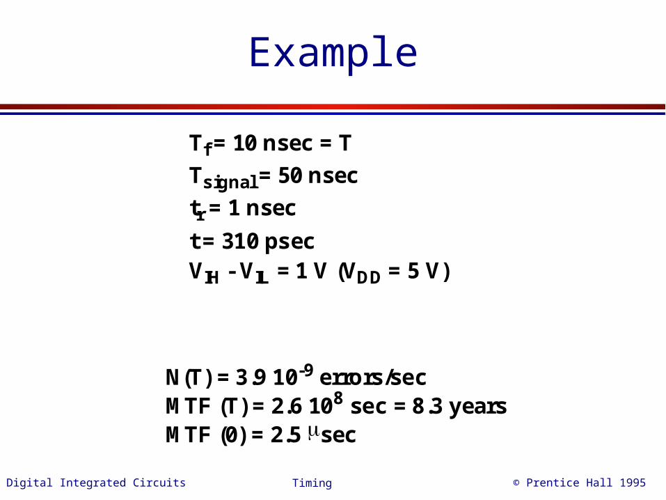
Example
Tf = 10 nsec = T
Tsignal = 50 nsec
tr = 1 nsec
t = 310 psecVIH - VIL = 1 V (VDD = 5 V)
N(T) = 3.9 10-9 errors/secMTF (T) = 2.6 108 sec = 8.3 yearsMTF (0) = 2.5 sec
Digital Integrated Circuits © Prentice Hall 1995Timing
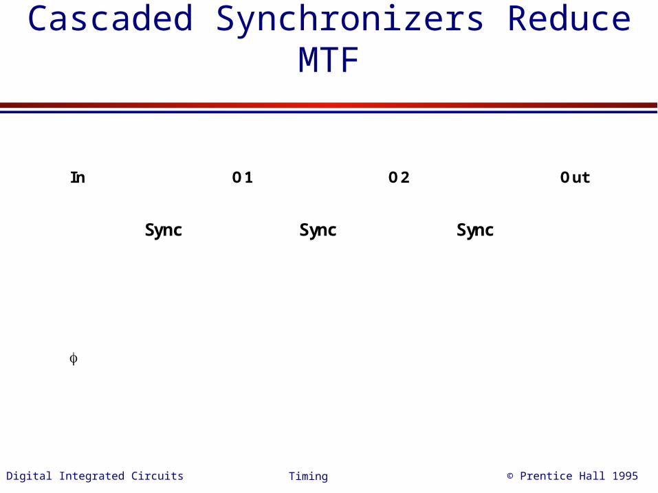
Cascaded Synchronizers Reduce MTF
Sync Sync Sync
In OutO1 O2
Digital Integrated Circuits © Prentice Hall 1995Timing
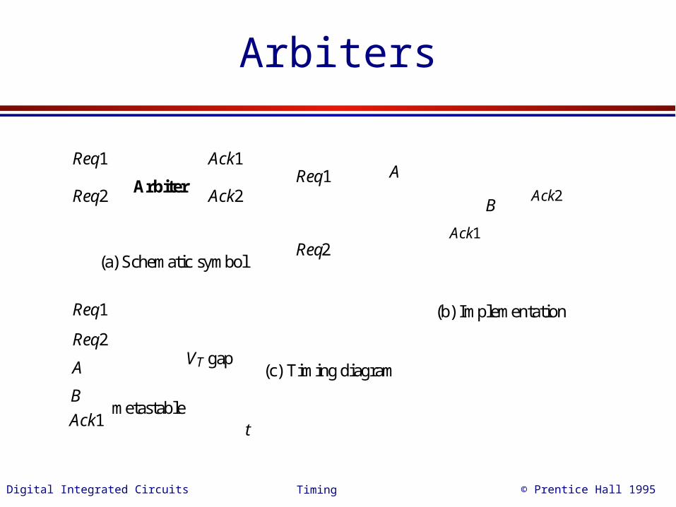
Arbiters
Req1
Req2
Req1
Req2
Ack1
Ack2Arbiter
Ack1
Ack2
(a) Schematic symbol
(b) Implementation
A
B
Req1
Req2
A
B
Ack1 t
(c) Timing diagramVT gap
metastable
Digital Integrated Circuits © Prentice Hall 1995Timing
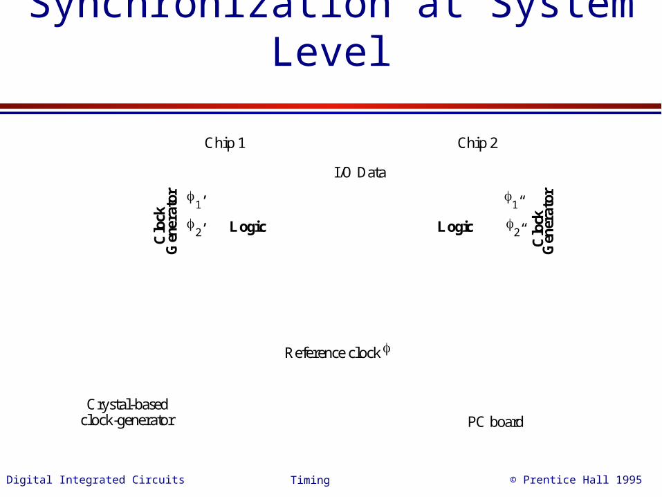
Synchronization at System Level
Reference clock
PC board
Chip 1 Chip 2
Logic Logic
I/O Data
1’
2’
1“
2“
Crystal-basedclock-generator
Clo
ckG
ener
ator
Clo
ckG
ener
ator
Digital Integrated Circuits © Prentice Hall 1995Timing
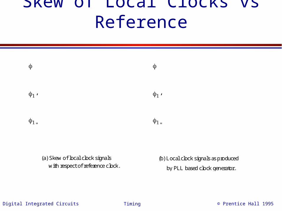
Skew of Local Clocks vs Reference
’
"
’
"
(a) Skew of local clock signals
with respect of reference clock.(b) Local clock signals as produced
by PLL based clock generator.
Digital Integrated Circuits © Prentice Hall 1995Timing
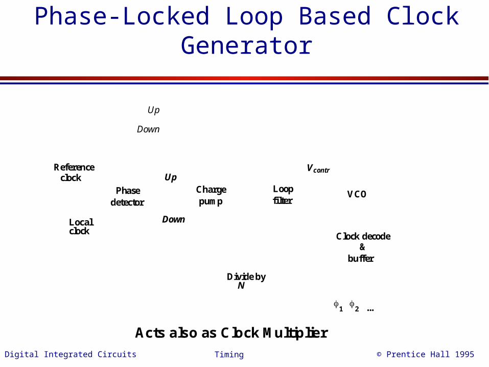
Phase-Locked Loop Based Clock Generator
Phasedetector
Chargepump
Up
Down
Loopfilter
VCO
Clock decode &
buffer
Divide byN
Reference clock
Localclock
1 2 ...
Vcontr
Acts also as Clock Multiplier
Up
Down
Digital Integrated Circuits © Prentice Hall 1995Timing
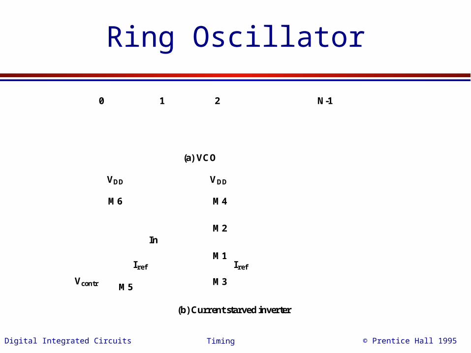
Ring Oscillator
0 1 2 N-1
In
VDD
M3
M1
M2
M4
M5
VDD
M6
Vcontr
(a) VCO
(b) Current starved inverter
Iref Iref
Digital Integrated Circuits © Prentice Hall 1995Timing
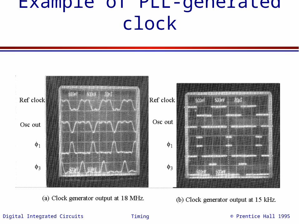
Example of PLL-generated clock