Embed Size (px)
Citation preview
Purdue UniversityPurdue e-Pubs
Open Access Theses Theses and Dissertations
Fall 2014
Digital Image Correlation Of HeterogeneousDeformations In Polycrystalline Material WithElectron Backscatter DiffractionJavier EsquivelPurdue University
Follow this and additional works at: https://docs.lib.purdue.edu/open_access_theses
Part of the Aerospace Engineering Commons, Computer Sciences Commons, and the MaterialsScience and Engineering Commons
This document has been made available through Purdue e-Pubs, a service of the Purdue University Libraries. Please contact [email protected] foradditional information.
Recommended CitationEsquivel, Javier, "Digital Image Correlation Of Heterogeneous Deformations In Polycrystalline Material With Electron BackscatterDiffraction" (2014). Open Access Theses. 321.https://docs.lib.purdue.edu/open_access_theses/321


DIGITAL IMAGE CORRELATION OF HETEROGENEOUS DEFORMATIONS IN
POLYCRYSTALLINE MATERIAL WITH ELECTRON BACKSCATTER
DIFFRACTION
A Thesis
Submitted to the Faculty
of
Purdue University
by
Javier Esquivel
In Partial Fulfillment of the
Requirements for the Degree
of
Masters of Science in Aeronautics and Astronautics
December 2014
Purdue University
West Lafayette, Indiana

ii
For my parents, Jaime and Blanca, whose courage and strength made this possible.

iii
ACKNOWLEDGEMENTS
First and foremost, I would like to thank Dr. Michael Sangid for his enthusiasm, patience,
and guidance in the journey to complete this thesis. His confidence in my ability to
succeed within his research team was persistent from the day he offered me the great
opportunity. I would also like to thank the members of my committee, Dr. Alten F.
Grandt and Dr. James F. Doyle, not only for their knowledge, patience, and flexibility in
reviewing my work, but for stressing the importance of structures in aeronautics and
sparking my enthusiasm in the field.
Sincere thanks must be given to Purdue University for the challenging, yet nourishing,
environment it provided during my academic and professional growth. Specific thanks
to the School of Aeronautics and Astronautics for instilling in me a passion of air and
space that could not have been created anywhere else. Recognition should go to Jameson
Root, Jan Eberle, and Dr. David Bahr for the accessibility of their expertise and
equipment. I would like to thank Dave Raegan and John Phillips for their willingness to
accept the challenges presented to our laboratory and the excellent ability to solve them.
Thanks to Chuck Harrington of the ECE machine shop for being committed to the
manufacturing needs of this project.
The members of the ACME lab, specifically Todd Book, Matthew Durbin, Tony
Favaloro, Megan Kinney, Dr. Bhisham Sharma, Saikumar Reddy Yeratapally, Andrea
Rovinelli, and Ajey Venkataraman, provided the atmosphere to appreciate challenges, the
intellect to reason, and most importantly, the sincere friendships to be able to laugh.

iv
I want to thank my family for harboring the source of motivation needed to endure the
challenges of this journey. Without the sacrifice and hard work of my mother and father,
their American Dream would be just that - a dream. Thank you to my brothers, Alfredo
and Jaime, for being the role models I needed in my life and for always challenging me to
improve. Thank you to my little sister, Sophia, for reminding me to stay young and enjoy
the small things. Lastly, I want to thank my wife and best friend, Anita, whose love
accompanied me every step of the way.

v
TABLE OF CONTENTS
Page
LIST OF FIGURES ......................................................................................................... viii
LIST OF TABLES ........................................................................................................... viii
NOMENCLATURE .......................................................................................................... xi
ABSTRACT ...................................................................................................................... xii
CHAPTER 1. INTRODUCTION ....................................................................................... 1
CHAPTER 2. LITERATURE REVIEW ............................................................................ 3
2.1 Digital Image Correlation ..........................................................................................3
2.1.1 Image Acquisition ...............................................................................................3
2.1.2 Two-Dimensional Strain Mapping Model ..........................................................4
2.1.3 Speckle Patterning ..............................................................................................7
2.1.4 Applications ........................................................................................................8
2.1.5 Microstructure Sensitive DIC .............................................................................9
CHAPTER 3. MULT-SCALE DIGITAL IMAGE CORRELATION ............................. 12
3.1 Overview ..................................................................................................................12
3.2 Equipment ................................................................................................................13
3.2.1 Buehler Ecomet V & III Polisher .....................................................................13
3.2.2 MTI SEMtester 1000 EBSD Load Frame ........................................................13

vi
Page
3.2.3 Controller and Calibration ................................................................................15
3.2.4 Olympus BX51M ..............................................................................................15
3.3 Sample Preparation ..................................................................................................16
3.3.1 Sample Geometry .............................................................................................17
3.3.2 Polishing ...........................................................................................................17
3.3.3 Speckle Application ..........................................................................................20
3.4 Loading ....................................................................................................................22
3.5 Image Acquisition ....................................................................................................24
3.6 Correlation ...............................................................................................................25
CHAPTER 4. DIGITAL IMAGE CORRELATION USING SCANNING ELECTRON
MICROSCOPY................................................................................................................. 29
4.1 Overview ..................................................................................................................29
4.2 Equipment ................................................................................................................29
4.2.1 LECO LM247AT Microhardness Tester & Amh43 Software .........................29
4.2.2 PACE GIGA-0900 Vibratory Polisher .............................................................30
4.2.3 PHILIPS FEI XL-40 SEM ................................................................................31
4.3 Sample Preparation ..................................................................................................32
4.3.1 Fiducial Markers ...............................................................................................32
4.3.2 Vibropolishing ..................................................................................................34
4.3.3 Electron Backscatter Diffraction ......................................................................34
4.3.4 Gold Nanoparticle Speckle ...............................................................................36
4.4 Loading ....................................................................................................................37
4.5 Image Acquisition ....................................................................................................39

vii
Page
4.6 Correlation ...............................................................................................................40
4.7 Results and Analysis ................................................................................................41
CHAPTER 5. SUMMARY ............................................................................................... 44
CHAPTER 6. RECOMMENDATIONS AND FUTURE WORK ................................... 45
6.1 Overview ..................................................................................................................45
6.2 Recommendations ....................................................................................................45
6.2.1 Future Speckle ..................................................................................................45
6.2.2 Load Frame Issues ............................................................................................46
6.2.3 SEM-DIC Bias ..................................................................................................47
6.2.4 Crystallographic Analysis .................................................................................48
6.3 Future Work .............................................................................................................49
BIBLIOGRAPHY ............................................................................................................. 50
APPENDIX: SPECIMEN PART DRAWING ................................................................. 54

viii
LIST OF TABLES
Table Page
Table 1: MTI SEMtester 1000 EBSD parameters ............................................................ 14
Table 2: Image properties for Olympus BX51M at various magnifications .................... 24

ix
LIST OF FIGURES
Figure Page
Figure 1: Schematic of experimental configuration for correlation analysis [3] ................ 4
Figure 2: Modern DIC setup ............................................................................................... 4
Figure 3: "Illustration of differential motion estimation for 1-d problem" [7] ................... 5
Figure 4: Illustration of subset deformation [8] .................................................................. 7
Figure 5: Example speckle patterns developed over the past decades ................................ 8
Figure 6: Bone compression DIC results [30] .................................................................... 9
Figure 7: Strain quantified with respect to microstructure (2009-2010). ......................... 10
Figure 8: Strain quantified with respect to microstructure (2012-2013). ......................... 11
Figure 9: Buehler Ecomet V Polisher (left) and Buehler Ecomet III Polisher (right) ...... 13
Figure 10: MTI SEMtester 1000 EBSD under optical microscope .................................. 15
Figure 11: Olympus BX51M w/ SEMtester 1000 EBSD ................................................. 16
Figure 12: Sample geometry ............................................................................................. 17
Figure 13: Progressive polishing process ......................................................................... 18
Figure 14: Comet trails induced by particle embedding on OFHC Cu ............................. 19
Figure 15: Silicon oxide speckle application apparatus .................................................... 20
Figure 16: Silica oxide speckle on OFHC Cu ................................................................... 22
Figure 17: Tensile test set up on Olympus microscope .................................................... 22
Figure 18: Stress-strain curve of OFHC Cu, with images taken at circled points ........... 24
Figure 19: Digital magnification of speckle pattern ......................................................... 25
Figure 20: VIC-2D with reference image and subset shown ............................................ 26
Figure 21: Stress-strain curve of OFHC Cu calculated DIC strains ................................. 28
Figure 22: LECO LM247AT Microhardness Tester ........................................................ 30
Figure 23: PACE GIGA-0900 Vibratory Polisher ............................................................ 30

x
Figure Page
Figure 24: Philips FEI XL-40 used for in situ experiments .............................................. 31
Figure 25: Fiducial marker pattern with plastic deformation near indentations ............... 33
Figure 26: Final fiducial marker pattern used ................................................................... 33
Figure 27: XL-40 EBSD capabilities ................................................................................ 35
Figure 28: Microstructural data superimposed onto optical image .................................. 35
Figure 29: Gold nanoparticle surface layer preparation ................................................... 36
Figure 30: Gold nanoparticle speckle procedure .............................................................. 36
Figure 31: Gold nanoparticle speckle pattern ................................................................... 37
Figure 32: Modified port cover on XL-40 ........................................................................ 38
Figure 33: Loading profile executing inside of the XL-40 ............................................... 39
Figure 34: Reference image for Al 6061 and image stitch order ...................................... 40
Figure 35: Plastically deformed image for Al 6061 .......................................................... 40
Figure 36: Initial Guess Selection interface within VIC-2D ............................................ 41
Figure 37: Tensile strain map for 24.79 µm x 18.6 µm region ......................................... 42
Figure 38: Inverse pole figure of 100 µm x 100 µm region on Al 6061 sample .............. 43
Figure 39: Strain values with grain boundary outline overlay .......................................... 43
Figure 40: Stress-strain curve of Al 6061 ......................................................................... 46
Figure 41: Kammers and Daly, Experimental Mechanics, 53 (2013) .............................. 48

xi
NOMENCLATURE
AOI- Area of Interest
ACME - Advanced Computational Materials and Experimental Evaluation
DIC – Digital Image Correlation
EBSD – Electron Backscatter Diffraction
fcc- Face Centered Cubic
OFHC- Oxygen Free High Thermal Conductivity
s- Number of Slip Systems
SEM – Scanning Electron Microscope
n - Vector defining the normal to slip plane for system
ZSSD - zero-mean sum of square differences
- Slip System Number
xii
ABSTRACT
Esquivel, Javier M.S.A.A., Purdue University, December 2014. Strain Mapping of
Heterogeneous Deformation Using Digital Image Correlation with Electron Backscatter
Diffraction. Major Professor: Dr. Michael Sangid.
This work establishes the ability to conduct digital image correlation (DIC) investigations
at varying length scales. DIC allows for a computational method of strain field
measurements using multiple images to track random speckle patterns on material
surfaces. The use of a powder silicon oxide speckle allows for high optical magnification
correlation using conventional load frames. Self-assembling gold nanoparticles provide
sub-micron resolution speckle patterns to study microstructure influences on deformation
using scanning electron microscopy. The complex microstructure in aerospace grade
aluminum and nickel-based superalloys, give rise to varied deformation fields, which can
be studied using electron backscatter diffraction. Specimen preparation techniques,
speckle patterns, and image correlation analysis are discussed. Experimental
identification of strains at grain level can help validate computational crystal plasticity
finite element models, which in turn provide better predictive computational models.
1
CHAPTER 1. INTRODUCTION
Component failure is a result of deformation accumulating in small regions within a part.
In fact, strain localization is a precursor to material failure. Digital image correlation
(DIC) has become a valuable means to study strain in materials and components through
non-contact / non-destructive analysis. In this research, the fundamentals of strain
localization are enabled through the set-up of a unique experimental analysis.
The microstructure attributes are responsible for heterogeneous deformation. Defects
within the microstructure localize deformation and lead to incompatible strain. In this
study, structural alloys are the focus. Consequently the microstructure, in the form of
grains and grain boundaries, are attributed to microstructural sensitive heterogeneous
deformation. In polycrystalline deformation, a constitutive theory for heterogeneous
deformation is still lacking. Thus, it is necessary to elucidate these mechanisms through
detailed microstructural-sensitive experiments.
In the following research, the microstructure is characterized through electron backscatter
diffraction (EBSD), in order to identify a spatial map of local grain orientations. This
information is coupled with strain maps of local deformation via DIC. Following EBSD,
a fine speckle pattern is applied on the sample surface for DIC analysis. Previous work by
Dr. Sangid established optical microscope images at 31x magnification during interrupted
or ex situ testing with deformation accommodated by a servo-hydraulic load frame. In-
plane displacements were measured from DIC and the results were differentiated to
obtain three components of the plastic strain tensor (εxx, εyy, and εxy). The DIC resolution
was much smaller than the average grain size, which provides sub-grain level
deformation measurement accuracy. The advantage of such a measurement procedure is
that it enables quantitative analysis of the plastic strain fields in relation to the underlying
microstructure of the polycrystalline specimen.

2
In this research, the experimental system is developed within a scanning electron
microscope (SEM), in order to provide a higher resolution characterization of the
material’s strain. Furthermore, without needing to move the specimen for additional
microscopy, the experiment can be performed in situ to characterize the material’s strain.
This spatial information of strain localization relative to the microstructure is crucial for
the insights into heterogeneous deformation and failure within materials.
Chapter 2 describes a literature review of digital image correlation, including
advancements in speckle patterning and microstructure sensitive strain maps. Chapter 3
describes multi-scale DIC, including an overview of the equipment and procedures for
specimen preparation (including speckling). Further, the loading, imaging, and
correlation results within the SEM are discussed in Chapter 4. A summary of the
research along with recommendations for future work are discussed in Chapters 5 and 6.

3
CHAPTER 2. LITERATURE REVIEW
2.1 Digital Image Correlation
The history of digital image correlation (DIC) can be traced back to the early works and
studies of photogrammetry, the science of making measurements from images. Leonardo
da Vinci and Johan Heinrich Lambert were among the earliest to study this science in
1492 and 1759 respectively [1]. Photography still in the early stages of development
lacked computers to digitize the images and enable algorithms to compute strain fields. It
was not until the mid-1900s that advancements in imaging and computing began shaping
the way for image correlation that we know today. Rosenfeld discusses these imaging
advances in detail, stating, “almost as soon as digital computers became available, it was
realized that they could be used to process and extract information from digitized
images” [2].
2.1.1 Image Acquisition
Researchers at the University of South Carolina took the first steps in developing the
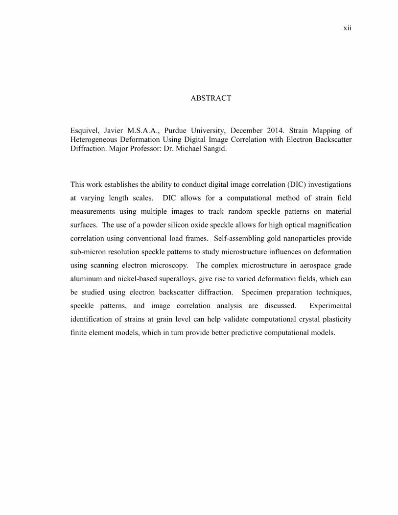
framework for computer-based deformation measurements. Figure 1 below shows the
early image acquisition model envisioned by Peters and Ranson [3]. An issue faced by
the lack of advanced imaging components, was the method in which data from camera
systems would be transferred and stored digitally to allow researchers to develop
algorithms.
4
Figure 1: Schematic of experimental configuration for correlation analysis [3]
As discussed in this work, the acquisition and storage of images using modern
technology, is done seamlessly through the use of controllers and software programs
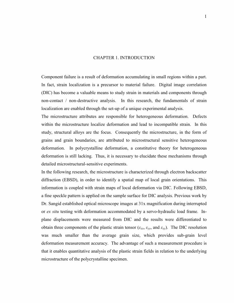
integrated with the hardware. Figure 2 below shows an example of a DIC setup that
contains the same components as outlined by Peters and Ranson. Images can now be
captured using sensors, triggers, and other automated methods. Additionally, images
come with valuable information such as precise timestamps, exposure time, etc.
Figure 2: Modern DIC setup
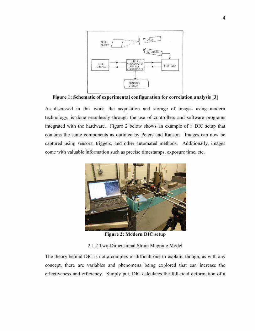
2.1.2 Two-Dimensional Strain Mapping Model
The theory behind DIC is not a complex or difficult one to explain, though, as with any
concept, there are variables and phenomena being explored that can increase the
effectiveness and efficiency. Simply put, DIC calculates the full-field deformation of a
5
material by tracking the movement of points created on the surface with images. The
researchers at South Carolina discuss theory in depth in their early works [3] [4] [5].
The displacement calculations done by DIC algorithms are not performed on individual
pixels, but rather many groups of pixels referred to as subsets. The reason being that
digitized representations of images have finite number of ways they can be represented.
For example, an 8-bit image, which is the most common format in cameras today, a value
of 0 corresponds to black, while the max value of 255 corresponds to white [6]. For a 16-
bit image, the max value of white corresponds to 65,535, meaning the different ways a
pixel can be represented is 65,535. For an 8-bit image with a resolution of 2576 x 2086
pixels, the chances that neighboring pixels have the same value is high, so tracking the
displacement of individual pixels would become nearly impossible.
Letting 𝐺(𝑥, 𝑡) represent the light intensity distribution, gray values, of a captured image,
tracking and correlation starts to become viable. Equations 2.1 and 2.2 show a gray value
distribution, approximated by a first order Taylor expansion, and after being displaced by
a small distance respectively [7]. Figure 3 shows this approximation in 1-D.
𝐺(𝑥 + 𝛥𝑥, 𝑡) = 𝐺(𝑥, 𝑡) +𝜕𝐺
𝜕𝑥𝛥𝑥
(2.1)
𝛥𝐺 = 𝐺(𝑥 − 𝛥𝑡) − 𝐺(𝑥, 𝑡)
(2.2)
Figure 3: "Illustration of differential motion estimation for 1-d problem" [7]

6
Applying this basic concept in 2-D leads to the brightness change constrain equation for
the optical flow
𝜕𝐺
𝜕𝑥+ v∙ 𝛻𝐺 = 0
(2.3)
Applying Equation 2.3 to a group of neighboring points or pixels leads to one of the main
equations in image correlation that allows computer algorithms to track the movement of
subsets.
[∆�̅�∆�̅�
] = −
[ ∑(
𝜕𝐺
𝜕𝑥)
2
∑(𝜕𝐺
𝜕𝑥
𝜕𝐺
𝜕𝑦)
∑(𝜕𝐺
𝜕𝑥
𝜕𝐺
𝜕𝑦) ∑(
𝜕𝐺
𝜕𝑦)2
] −1
[ 𝜕𝐺
𝜕𝑥∆𝑔
𝜕𝐺
𝜕𝑦∆𝑔
]
= [𝑢𝑣]
(2.4)
With subset tracking covered, the displacement of points within subsets can now be
calculated. Take the subset in Figure 4 with the center point denoted by P and an
arbitrary point denoted by Q. Equation 2.4 is used to calculate the displacement vectors
u and v for the P. The new position of any point within the subset can be represented by
a Taylor expansion shown in equations 2.5 and 2.6 [8].
�̃� = 𝑥0 + 𝑢0 +𝑑𝑢
𝑑𝑥Δ𝑥 +
𝑑𝑢
𝑑𝑦Δ𝑦 +
1
2
𝑑2𝑢
𝑑𝑥2Δ𝑥2 +
1
2
𝑑2𝑢
𝑑𝑦2Δ𝑦2 +
𝑑2𝑢
𝑑𝑥𝑑𝑦Δ𝑥Δ𝑦
(2.5)
�̃� = 𝑦0 + 𝑣0 +𝑑𝑣
𝑑𝑥Δ𝑥 +
𝑑𝑣
𝑑𝑦Δ𝑦 +
1
2
𝑑2𝑣
𝑑𝑥2Δ𝑥2 +
1
2
𝑑2𝑣
𝑑𝑦2Δ𝑦2 +
𝑑2𝑣
𝑑𝑥𝑑𝑦Δ𝑥Δ𝑦
(2.6)

7
Figure 4: Illustration of subset deformation [8]
These principles can be programmed and integrated into computational software such as
MatLab or Opticist, as done by Johns Hopkins University and The Catholic University of
America, or can be purchased as packaged standalone solutions. ARAMIS, ISTRA 4D,
StrainMaster, and Vic3D are popular commercial packages offered by Trilion, Dantec
Dynamics, LaVision Inc, and Correlated Solutions, respectively [9].
2.1.3 Speckle Patterning
Alongside improving the efficiency of correlation algorithms, creation and application of
speckle patterns for varying length scales is one of the main areas of focus in DIC. For
most metals, surface preparation is simple and inexpensive. Speckle patterns can be
applied to the entire specimen, allowing for investigation of entire planar surfaces.
Speckle patterns have evolved from using white paint [10], fine black ink [11] [12], and
uniform grids [13] [14],to nanolithography techniques [15] [16], silicon microparticles
[17], gold nanoparticles [18], and vapor deposits [19], amongst many other methods.
Figure 5 shows an example of a random isotropic speckle pattern created with silica
oxide powder and gold nanoparticles. Finer speckle patterns and better imaging
technologies have led to studies being held at smaller and smaller length scales.
8
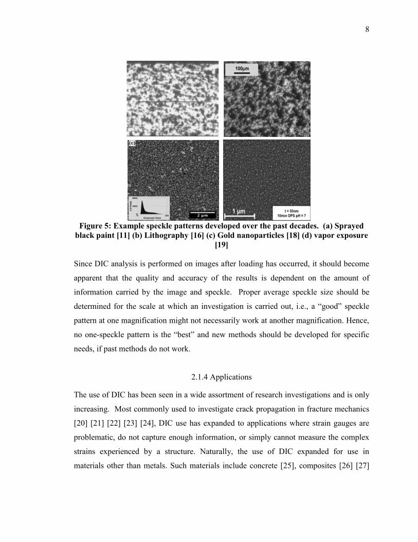
Figure 5: Example speckle patterns developed over the past decades. (a) Sprayed
black paint [11] (b) Lithography [16] (c) Gold nanoparticles [18] (d) vapor exposure
[19]
Since DIC analysis is performed on images after loading has occurred, it should become
apparent that the quality and accuracy of the results is dependent on the amount of
information carried by the image and speckle. Proper average speckle size should be
determined for the scale at which an investigation is carried out, i.e., a “good” speckle
pattern at one magnification might not necessarily work at another magnification. Hence,
no one-speckle pattern is the “best” and new methods should be developed for specific
needs, if past methods do not work.
2.1.4 Applications
The use of DIC has been seen in a wide assortment of research investigations and is only
increasing. Most commonly used to investigate crack propagation in fracture mechanics
[20] [21] [22] [23] [24], DIC use has expanded to applications where strain gauges are
problematic, do not capture enough information, or simply cannot measure the complex
strains experienced by a structure. Naturally, the use of DIC expanded for use in
materials other than metals. Such materials include concrete [25], composites [26] [27]

9
[28], and biological materials such as bone [29] [30]and human skin [31]. Steps are
continually being taken to expand the length scale range at which DIC can be effectively
used.
Figure 6: Bone compression DIC results [30]
2.1.5 Microstructure Sensitive DIC
Steps are constantly being taken to increase the resolution and decrease the length scale at
which DIC can be effectively used. This represents a powerful tool when combined with
characterization of the microstructure, to assess the heterogeneous deformation, damage
mechanisms, or fatigue behavior. Here, a review of the microstructure-sensitive strain
maps is as follows.
In 2009, Tschopp, et al., performed in situ strain mapping in a SEM of a Ni-base
superalloy, Rene 88DT [32]. Their results are shown in Figure 7a and represent, to the
author’s knowledge, the first time microstructure sensitive strain maps were performed to
analyze polycrystalline deformation. As shown in Figure 7b, Clair, et al., used Kernel
average misorientation to investigate local strain near triple points [33]. Abuzaid,
Sangid, et al., used DIC-EBSD method to investigate polycrystalline deformation [34].
As shown in Figure 7c, an ex situ technique was used at 31X to investigate a large area of
interest (1mm by 0.8 mm). The results were decomposed, using a Bishop-Hill
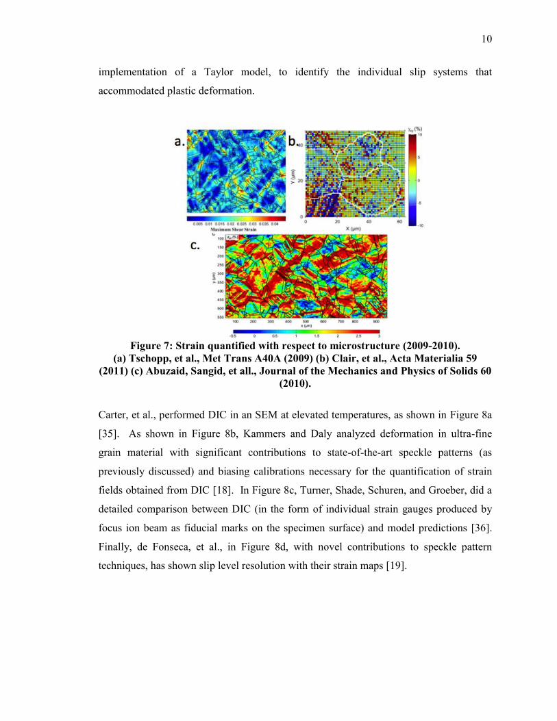
10
implementation of a Taylor model, to identify the individual slip systems that
accommodated plastic deformation.
Figure 7: Strain quantified with respect to microstructure (2009-2010).
(a) Tschopp, et al., Met Trans A40A (2009) (b) Clair, et al., Acta Materialia 59
(2011) (c) Abuzaid, Sangid, et all., Journal of the Mechanics and Physics of Solids 60
(2010).
Carter, et al., performed DIC in an SEM at elevated temperatures, as shown in Figure 8a
[35]. As shown in Figure 8b, Kammers and Daly analyzed deformation in ultra-fine
grain material with significant contributions to state-of-the-art speckle patterns (as
previously discussed) and biasing calibrations necessary for the quantification of strain
fields obtained from DIC [18]. In Figure 8c, Turner, Shade, Schuren, and Groeber, did a
detailed comparison between DIC (in the form of individual strain gauges produced by
focus ion beam as fiducial marks on the specimen surface) and model predictions [36].
Finally, de Fonseca, et al., in Figure 8d, with novel contributions to speckle pattern
techniques, has shown slip level resolution with their strain maps [19].

11
Figure 8: Strain quantified with respect to microstructure (2012-2013).
(a) Carter, Mills, et al., Superalloys (2012) . (b) Kammers and Daly, Experimental
Mechanics, 53 (2013). (c) Turner, Shade, Schuren, Groeber, Modelling Simul.
Mater. Sci. Eng. 21 (2013). (d) F. Di Gioacchino and J. Quinta da Fonseca,
experimental Mechanics 53 (2013).

12
CHAPTER 3. MULT-SCALE DIGITAL IMAGE CORRELATION
3.1 Overview
Although the use of digital image correlation (DIC) is widely accepted in experimental
mechanics, there are several variables that require tuning before results can be used in
meaningful studies. Development of a framework to obtain strain localization
measurements, using popular DIC methods, was one of the main goals of this work.
Although the steps are few and relatively straightforward, the quality and reproducibility
of results varies depending on the methods used for each step. The general steps required
for reliable tracking of surface deformation include:
1. Polish
2. Speckle
3. Deformation
4. Image Acquisition
5. Correlation/Analysis
The equipment and steps developed for use in the Advanced Computational Materials
and Experimental Evaluation (ACME) laboratory in the School of Aeronautics and
Astronautics at Purdue University will be covered in detail in the following sections.
Chapter 3 will focus on the methods developed for multi-scale DIC experiments that can
be conducted in the ACME laboratory itself, while Chapter 4 will discuss the methods
developed for in situ scanning electron microscope DIC (SEM-DIC) experiments that are
carried out in vacuum conditions.
13
3.2 Equipment
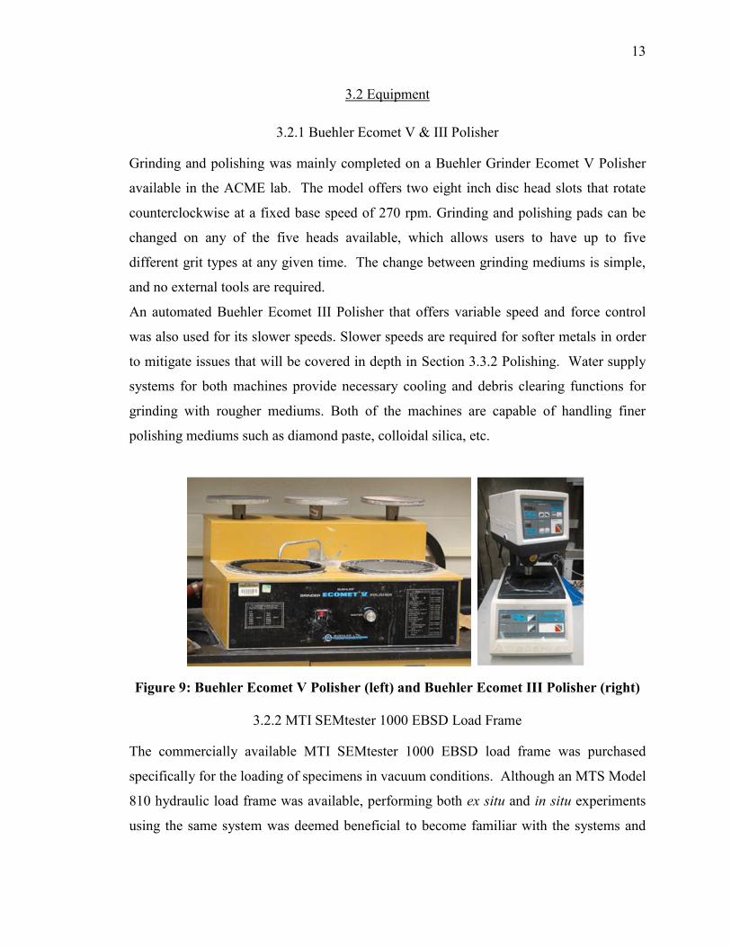
3.2.1 Buehler Ecomet V & III Polisher
Grinding and polishing was mainly completed on a Buehler Grinder Ecomet V Polisher
available in the ACME lab. The model offers two eight inch disc head slots that rotate
counterclockwise at a fixed base speed of 270 rpm. Grinding and polishing pads can be
changed on any of the five heads available, which allows users to have up to five
different grit types at any given time. The change between grinding mediums is simple,
and no external tools are required.
An automated Buehler Ecomet III Polisher that offers variable speed and force control
was also used for its slower speeds. Slower speeds are required for softer metals in order
to mitigate issues that will be covered in depth in Section 3.3.2 Polishing. Water supply
systems for both machines provide necessary cooling and debris clearing functions for
grinding with rougher mediums. Both of the machines are capable of handling finer
polishing mediums such as diamond paste, colloidal silica, etc.
Figure 9: Buehler Ecomet V Polisher (left) and Buehler Ecomet III Polisher (right)
3.2.2 MTI SEMtester 1000 EBSD Load Frame
The commercially available MTI SEMtester 1000 EBSD load frame was purchased
specifically for the loading of specimens in vacuum conditions. Although an MTS Model
810 hydraulic load frame was available, performing both ex situ and in situ experiments
using the same system was deemed beneficial to become familiar with the systems and

14
allow for a comparison of the two methods. The combination of DIC with electron
backscatter diffraction scans was an ultimate goal of this project; therefore the use of the
frame to be used inside of the scanning electron microscope (SEM) was preferred.
The MTI load frame offers interchangeable load cells of 10 lb, 100 lb, or 1000 lb, with
smaller load cells providing higher accuracy at the corresponding lower loads. The
1000lb load cell was used for all of the experiments in this work, and offered a load
accuracy of ±2 lb. Table 1 highlights some of the additional parameters offered by the
SEMtester 1000 EBSD.
Table 1: MTI SEMtester 1000 EBSD parameters
Max. Load Capability 1000 lb (4500 N) [Optional
100 lb]
Max. Sample Size (L x W
x T)
53mm x 10mm x 2.5mm
Min. Sample Size (L x
W)
43mm x 10mm
Max. Strain Travel 10mm
Load Cell Accuracy ±.2% of load range
Heating Capabilities Ambient to 1200°C(±5.0°C
Control)
Data Acquisition Rate 1 kHz max

15
Figure 10: MTI SEMtester 1000 EBSD under optical microscope
3.2.3 Controller and Calibration
The MTI SEMtester EBSD 1000 was shipped, calibrated, and certified by MTI engineers.
Installation of the controller software provides the machine with the appropriate
calibration files for the corresponding load cells. The controller requires a USB
connection to the computer system and standard power outlet. Three main wires from the
load frame to the controller provide the necessary signals for data acquisition. Loose or
disconnected wires will result in faulty load frame data. Thorough inspection of all
connections is recommended before running any loading profiles, as this was the source
of troubleshooting efforts early on. An optional fourth connection provides heating
capabilities.
3.2.4 Olympus BX51M
The optical microscope used in this study offered an excellent combination of utility and
performance. The advantage of using an optical microscope over a scanning electron
microscope is the ease and relative quickness of acquiring images and running tests.
However, a major drawback is the lack of higher magnification (>100x) images that can
be acquired.
The particular stage on this microscope was sufficiently large to allow the SEMtester to
rest evenly and without physical obstacles. As shown below in Figure 11, the SEMtester
load frame can easily be placed wherever a camera is available.
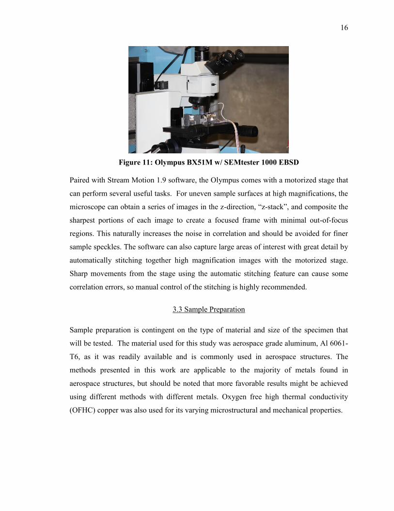
16
Figure 11: Olympus BX51M w/ SEMtester 1000 EBSD
Paired with Stream Motion 1.9 software, the Olympus comes with a motorized stage that
can perform several useful tasks. For uneven sample surfaces at high magnifications, the
microscope can obtain a series of images in the z-direction, “z-stack”, and composite the
sharpest portions of each image to create a focused frame with minimal out-of-focus
regions. This naturally increases the noise in correlation and should be avoided for finer
sample speckles. The software can also capture large areas of interest with great detail by
automatically stitching together high magnification images with the motorized stage.
Sharp movements from the stage using the automatic stitching feature can cause some
correlation errors, so manual control of the stitching is highly recommended.
3.3 Sample Preparation
Sample preparation is contingent on the type of material and size of the specimen that
will be tested. The material used for this study was aerospace grade aluminum, Al 6061-
T6, as it was readily available and is commonly used in aerospace structures. The
methods presented in this work are applicable to the majority of metals found in
aerospace structures, but should be noted that more favorable results might be achieved
using different methods with different metals. Oxygen free high thermal conductivity
(OFHC) copper was also used for its varying microstructural and mechanical properties.
17
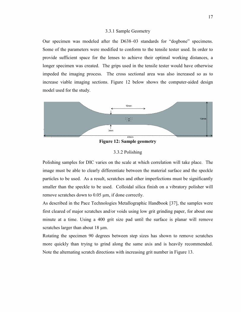
3.3.1 Sample Geometry
Our specimen was modeled after the D638–03 standards for “dogbone” specimens.
Some of the parameters were modified to conform to the tensile tester used. In order to
provide sufficient space for the lenses to achieve their optimal working distances, a
longer specimen was created. The grips used in the tensile tester would have otherwise
impeded the imaging process. The cross sectional area was also increased so as to
increase viable imaging sections. Figure 12 below shows the computer-aided design
model used for the study.
Figure 12: Sample geometry
3.3.2 Polishing
Polishing samples for DIC varies on the scale at which correlation will take place. The
image must be able to clearly differentiate between the material surface and the speckle
particles to be used. As a result, scratches and other imperfections must be significantly
smaller than the speckle to be used. Colloidal silica finish on a vibratory polisher will
remove scratches down to 0.05 µm, if done correctly.
As described in the Pace Technologies Metallographic Handbook [37], the samples were
first cleared of major scratches and/or voids using low grit grinding paper, for about one
minute at a time. Using a 400 grit size pad until the surface is planar will remove
scratches larger than about 18 µm.
Rotating the specimen 90 degrees between step sizes has shown to remove scratches
more quickly than trying to grind along the same axis and is heavily recommended.
Note the alternating scratch directions with increasing grit number in Figure 13.

18
Figure 13: Progressive polishing process. (a) Standard machine finish at 5X
magnification. (b) 400 grit finish at 5X magnification. (c) 600 grit finish at 5X
magnification. (d) 1200 grit finish at 5X magnification. (e) Colloidal silica finish at
5X magnification. (f) Vibratory polishing finish at 5X magnification.
It is important to use the water system on the grinding machines to prevent heating, and
more importantly, serve as a lubricant to prevent the fracture of the grinding medium into
the sample. Silicon carbide paper, which is generally the next medium in the polishing
procedure, was used at 800 and 1200 grit sizes for one minute at the recommended 100
rpm speeds. Although low speeds were used, silicon carbide particles occasionally
embedded into the soft aluminum samples. This may have been a result of uneven force
application or uneven grinding pad. Figure 14 shows an example of smeared silicon
carbide particles and pulled oxide inclusions. These are extremely undesirable for EBSD
investigations, as the surface becomes deformed and uneven, causing electrons to scatter
sporadically. If there are too many embedded particles, re-grinding the sample at lower
grit is necessary, as increasing grit number will take too long to remove large
imperfections.
(a) (b) (c)
(d) (e) (f)

19
Figure 14: Comet trails induced by particle embedding on OFHC Cu. Image taken
at 5X.
Upon finishing the 1200 grit grinding, the finished polish was achieved in one of three
ways. Diamond paste of 6 µm, 3 µm, and 1 µm sizes can easily be used for harder metals
such as titanium or steel, but runs a high risk of embedding in softer metals such as
aluminum and copper, so it was not used for this study. Instead, alumina polish on
NAPAAD pads was used in 1 µm, 0.3 µm, and 0.005 µm steps. Using the same speeds
of about 100rpm for about 1 minute on each alumina size removed the large scratches
caused by grinding. Also, 0.005 µm colloidal silica polishing suspension was used on the
same type of NAPAAD pads. Stepping from 1200 grit paper to 0.005µm colloidal silica
suspensions was possible, but took an average of 45 minutes. Upon reaching a “mirror”
finish, deionized water was run on the NAPAAD pad to prevent crystallization of
colloidal silica on the surface of the sample. A strong jet of water is needed to clear the
surface of any stubborn aggregates.
It is strongly encouraged to view the surface of the sample using an optical microscope
before continuing, as any voids or comet tails created by the oxide inclusions can
dramatically diminish the quality of speckle patterns, depending on the length scale of
interest. It is much more efficient to view the sample at the highest optical magnification
to spot any potential blemishes on the sample before using valuable SEM time to spot
them. While viewing the sample on the Olympus microscope, it was kept barely
submerged in a petri dish to prevent crystallization. Once a desired polish was viewed,
the sample was slowly dried with compressed air and stored in a sealed container.

20
3.3.3 Speckle Application
The ACME lab had previously gathered the equipment necessary to apply a silicon IV
oxide speckle to metallic samples [38]. Put simply, silica oxide particles were air sprayed
through a filter onto an electrostatically charged metallic sample to create a fine pattern.
This method is easily adjusted for different macroscopic length scales by simply
changing the size of the particles and the density of the spray. The method, however, had
not been used by the ACME laboratory to run DIC tensile tests and obtain valid strain
values. It was thought to be prudent to run a DIC tensile test to both test the correlation
software and our understanding of its parameters, as well as provide establish a reliable
method for applying silicon speckles to larger scale DIC tests, such as fatigue crack
experiments. Figure 15 shows the set up for this particular speckle application method.
Figure 15: Silicon oxide speckle application apparatus
After the sample has been properly polished, viewed under the magnification of interest,
and is deemed free of large scratches and imperfections, it should be handled with great
care, as any contact with fingers or even gloves will damage the quality of speckle
applied. The sample should be completely dry and, if not stored in a container, sprayed
with the compressed air gun to remove any dust particles that might have found their way
onto the surface. The sample needs be standing upright on its own and it was found that

21
a simple cardboard cutout of the specimen was an easy way of doing so. This allows the
specimen to fit snugly into the cardboard and allows the cardboard to be placed against
the back wall of the fume hood.
An Eastwood HotCoat Powder Coating System was used to create the voltage necessary
to allow the silicon particles to attach to the specimen. The system was always checked
to ensure that it was off and not running any current. Alligator clips were attached to a
section of the sample that were not going to be imaged, for example the grip sections.
The sample was placed in an upright freestanding position and a piece of filter fabric was
placed as close as possible to the sample without touching the surface. A distance of
about one inch or closer usually worked very well.
It was ensured that the appropriate size silicon particles were inside of the spray bottle
and that it was roughly ¼ of the way full. Next, the spray bottle was attached to the
compressed air hose and the pressure was checked to be at the desired levels. For this
particular application, a pressure of around 15 psi was discovered to work adequately.
As a safety precaution, electrical insulating gloves were worn as soon as power was given
to the HotCoat system. With gloves on, the spray gun was placed about 4-6 inches from
the filter, the HotCoat system power button pressed, and the gun sprayed in a circular or
“back and forth” manner for 10-20 seconds in short 2-3 second bursts. Bursts were
required due to the loss of pressure when the gun was used. Depending on the size of the
speckle used and the magnitude of the zoom used for images, the time required to spray
the sample will change. Figure 16 below shows a section speckle created on the sample.
22
Figure 16: Silica oxide speckle on OFHC Cu
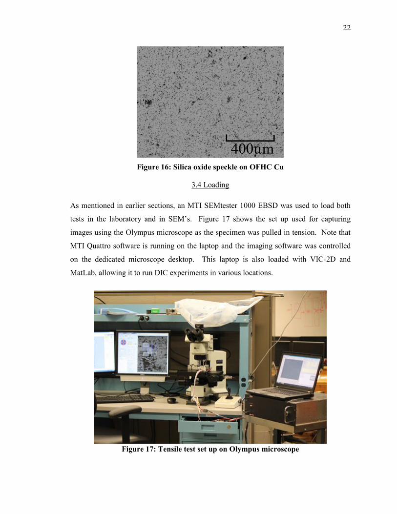
3.4 Loading
As mentioned in earlier sections, an MTI SEMtester 1000 EBSD was used to load both
tests in the laboratory and in SEM’s. Figure 17 shows the set up used for capturing
images using the Olympus microscope as the specimen was pulled in tension. Note that
MTI Quattro software is running on the laptop and the imaging software was controlled
on the dedicated microscope desktop. This laptop is also loaded with VIC-2D and
MatLab, allowing it to run DIC experiments in various locations.
Figure 17: Tensile test set up on Olympus microscope

23
The MTI controller software can be programmed to run various loading profiles based on
stress or crosshead displacement. Experiments were run using displacement control to
allow for the calculation of engineering strain in the generated stress-displacement data.
To properly obtain the mechanical properties of the sample, attention should be given
when placing the sample in the SEMtester. Four wedges, teeth, and cap screws took care
of the specimen grip. The crossheads moved together at the same rates to prevent large
translations in captured images. The center of the sample should theoretically experience
less rigid body translation than a load frame that fixes one end of its sample.
Before testing any sample, proper pre-loading practice was followed. This consisted of
clamping the wedge teeth down using the cap screws to apply finger tight torque. The
machine crossheads were then manually “jogged” or displaced until a force of about 10%
max load was reported by the Quattro software. This will allow the teeth to “bite” down
onto the sample and prevent slippage of the sample at the grips. The machine was then
“jogged” down until the force reported was around 1-5N. The cap screws
The Quattro software commanded displacements in increments of 0.05mm until sample
failure. Upon reaching a desired displacement interval, the load frame held the position
until instructed to continue by the user. This allowed for the acquisition of images.
Figure 18 shows stress-strain curve generated by the loading profile. The circled points
denote the instances at which images were taken. In order to capture the entire gauge
area, multiple images were taken and stitched together as explained in the following
section.

24
Figure 18: Stress-strain curve of OFHC Cu with images taken at circled points
3.5 Image Acquisition
When using the SEMtester on the Olympus microscope, it is advised that the grips be
separated enough to allow the lenses to achieve its required working distance. Objective
lenses are available at 5X, 10X, 20X, 50X, and 100X. Images can be captured using 25
bit RGB color or 8 bit grayscale at a resolution of 2048 x 1532 pixels. Information on the
image properties available using the Olympus BX51M are shown below in Table 2.
Table 2: Image properties for Olympus BX51M at various magnifications
Objective
Lens
Field of View
(µm)
Calibration
(µm /pixel)
Working
Distance
(µm)
Subset Size
at 31 pixels
(µm)
5X 2642 x 1981 2.58 19600 79.98
10X 1321 x 991 1.29 10600 39.99
20X 661 x 496 0.645 9600 20.00
50X 262 x 196.5 0.25583 380 7.93
100X 130.6 x 98 0.12758 210 3.96
0
20
40
60
80
100
120
140
160
180
200
0 0.02 0.04 0.06 0.08 0.1
Str
ess
(M
Pa
)
Strain
Stres vs. Strain - Sample C02
25
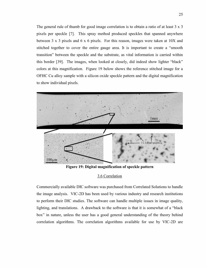
The general rule of thumb for good image correlation is to obtain a ratio of at least 3 x 3
pixels per speckle [7]. This spray method produced speckles that spanned anywhere
between 3 x 3 pixels and 6 x 6 pixels. For this reason, images were taken at 10X and
stitched together to cover the entire gauge area. It is important to create a “smooth
transition” between the speckle and the substrate, as vital information is carried within
this border [39]. The images, when looked at closely, did indeed show lighter “black”
colors at this magnification. Figure 19 below shows the reference stitched image for a
OFHC Cu alloy sample with a silicon oxide speckle pattern and the digital magnification
to show individual pixels.
Figure 19: Digital magnification of speckle pattern
3.6 Correlation
Commercially available DIC software was purchased from Correlated Solutions to handle
the image analysis. VIC-2D has been used by various industry and research institutions
to perform their DIC studies. The software can handle multiple issues in image quality,
lighting, and translations. A drawback to the software is that it is somewhat of a “black
box” in nature, unless the user has a good general understanding of the theory behind
correlation algorithms. The correlation algorithms available for use by VIC-2D are
26
covered in detail by Sutton [7]. For this study, the zero-mean sum of square differences
(ZSSD) criterion was used to negate artifacts of lighting in results.
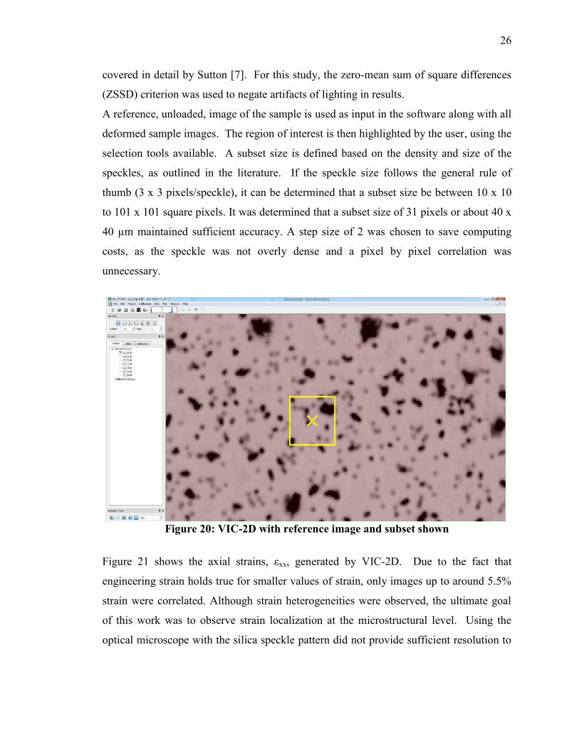
A reference, unloaded, image of the sample is used as input in the software along with all
deformed sample images. The region of interest is then highlighted by the user, using the
selection tools available. A subset size is defined based on the density and size of the
speckles, as outlined in the literature. If the speckle size follows the general rule of
thumb (3 x 3 pixels/speckle), it can be determined that a subset size be between 10 x 10
to 101 x 101 square pixels. It was determined that a subset size of 31 pixels or about 40 x
40 µm maintained sufficient accuracy. A step size of 2 was chosen to save computing
costs, as the speckle was not overly dense and a pixel by pixel correlation was
unnecessary.
Figure 20: VIC-2D with reference image and subset shown
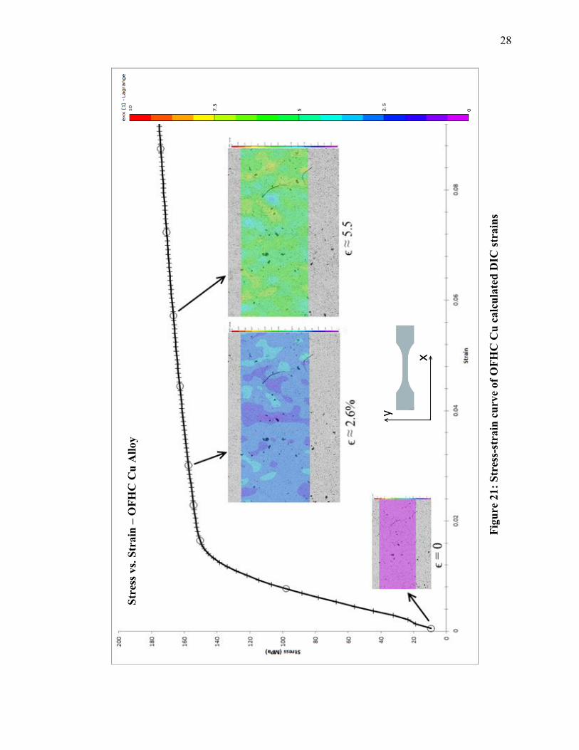
Figure 21 shows the axial strains, εxx, generated by VIC-2D. Due to the fact that
engineering strain holds true for smaller values of strain, only images up to around 5.5%
strain were correlated. Although strain heterogeneities were observed, the ultimate goal
of this work was to observe strain localization at the microstructural level. Using the
optical microscope with the silica speckle pattern did not provide sufficient resolution to

27
bring these phenomena to light. Attempting to create a denser speckle by spraying more
silica powder on the sample resulted in non-uniform clumps that rendered image areas
useless. Recommendations and possible solutions for this method are described in
Chapter 6. The following chapter discusses different imaging and speckle techniques that
provided much higher resolution at the scale of interest.
28
Str
ess
vs.
Str
ain
– O
FH
C C
u A
lloy
Fig
ure
21
: S
tres
s-st
rain
cu
rve
of
OF
HC
Cu
calc
ula
ted
DIC
str
ain
s

29
CHAPTER 4. DIGITAL IMAGE CORRELATION USING SCANNING ELECTRON
MICROSCOPY
4.1 Overview
The same basic DIC principles were applied to perform experiments inside of scanning
electron microscopes (SEM). However, several additional steps were required in order to
conduct loading experiments in such conditions. The additional preparation and
methodologies for SEM-DIC is explored. The complete steps are as follows:
1. Polish
2. Fiducial Markers
3. EBSD
4. Speckle
5. Deformation
6. Image Acquisition
7. Correlation/Analysis
4.2 Equipment
4.2.1 LECO LM247AT Microhardness Tester & Amh43 Software
Fiducial markers were created using the LECO LM247AT in the form of hardness
indentations. This system offers the ability to control the force used to make
indentations, with 10, 25, 50, 100, 500, and 1000 grams of force available. If any
hardness parameters (Vickers, Brinell, etc.) are known, the size of the indentation can be
approximated by the software with some level of confidence. Depending on your
material, 5-100µm hardness indentations can be made. The Amh43 software also allows
the user to move the micrometer stage in the x, y, and z, directions, as well as define
indentation patterns that will be carried out automatically by the machine. The software

30
automatically measures the size and exact coordinates of the indentations in relation to
the xyz coordinate system created by the software interface. The fiducial marks were
outside the area of interest, not to influence the mechanical behavior of the material being
imaged.
Figure 22: LECO LM247AT Microhardness Tester
4.2.2 PACE GIGA-0900 Vibratory Polisher
The machine used for the final step in preparation of EBSD scans or high magnification
imaging, is the PACE Technologies GIGA-0900 Vibratory Polisher. It utilizes vibrations
to remove smearing of oxides and even out microscopic bumps on the surface. The user
is able to change the vibration frequency and voltage, for varying size and weight of
samples. Colloidal silica should be poured onto the polishing pad until the entire surface
is covered. In general, this machine will only be used for microscopic imperfections in
the region of interest when microstructural information will be extracted.
Figure 23: PACE GIGA-0900 Vibratory Polisher
31
The PACE GIGA-0900 has optional weights that can be added to the sample in order to
apply a force to smaller samples that cannot rely on gravity. The vibratory polisher
should be spinning the sample about the center as an indication of an adequate polish.
Upon every polish, the polishing pad should be removed, as dried colloidal silica will
scratch the surface of any future samples.
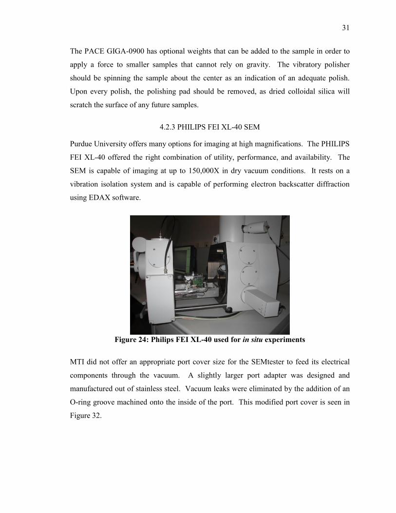
4.2.3 PHILIPS FEI XL-40 SEM
Purdue University offers many options for imaging at high magnifications. The PHILIPS
FEI XL-40 offered the right combination of utility, performance, and availability. The
SEM is capable of imaging at up to 150,000X in dry vacuum conditions. It rests on a
vibration isolation system and is capable of performing electron backscatter diffraction
using EDAX software.
Figure 24: Philips FEI XL-40 used for in situ experiments
MTI did not offer an appropriate port cover size for the SEMtester to feed its electrical
components through the vacuum. A slightly larger port adapter was designed and
manufactured out of stainless steel. Vacuum leaks were eliminated by the addition of an
O-ring groove machined onto the inside of the port. This modified port cover is seen in
Figure 32.

32
4.3 Sample Preparation
Preparation of the samples for microstructural analysis followed the same steps outlined
in the previous section of this paper, with the addition of fiducial markers, vibropolishing,
and EBSD scanning. Fiducial markers are generally reserved for experiments that will
load, image, move and re-image samples. Vibropolishing is the final step to remove any
microscopic surface deformations or misorientations, including plastic deformation
caused by microindentations.
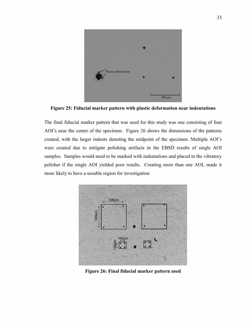
4.3.1 Fiducial Markers
Fiducial markers were used in this study to establish an area of interest and properly
overlay microstructure maps onto strain maps. The easiest and most common method of
creating fiducial markers was through the creation of microindentations. These
indentations were created through the use of the microindenter introduced in Section
4.2.1 LECO LM247AT Microhardness Tester & Amh43 Software. When imaging a very
small region of a sample, it can become troublesome to find the same region when a
properly polished sample is presented. The larger indentations created in this study were
used simply to more quickly find the region of interest. Figure 25 shows a sample pattern
of microindentations with apparent plastic deformation on one of the indents created with
a larger force. The larger indentation was created to denote the center of the specimen,
and the smaller indentations create a 400 µm x 400 µm area of interest (AOI). The larger
indentation was created with 50 grams of force, while the smaller indents were created
with 10 grams of force. In order to avoid plastic deformation other researchers have
opted to use focus ion beams (FIB) to deposit platinum markers, or have forgone the
fiducial markers entirely [18].
33
Figure 25: Fiducial marker pattern with plastic deformation near indentations
The final fiducial marker pattern that was used for this study was one consisting of four
AOI’s near the center of the specimen. Figure 26 shows the dimensions of the patterns
created, with the larger indents denoting the midpoint of the specimen. Multiple AOI’s
were created due to mitigate polishing artifacts in the EBSD results of single AOI
samples. Samples would need to be marked with indentations and placed in the vibratory
polisher if the single AOI yielded poor results. Creating more than one AOI, made it
more likely to have a useable region for investigation
Figure 26: Final fiducial marker pattern used
34
4.3.2 Vibropolishing
After creating a suitable fiducial indentation pattern, the samples were taken to the PACE
vibratory polisher to remove and residual stress that may have been created during the
indentation process. Samples were evenly placed on the available mounts using double
sided carbon tape. The polisher was checked to have a clean 9-inch NAPAAD polishing
pad and had 0.05 µm colloidal silica poured on it. The machine inputs were adjusted so
that the sample slowly rotated around the surface of the pad. For the samples in this
study, 158 volts and a frequency of 65.5 hertz were the parameters used to achieve
sufficient movement within the vibropolisher Since the aluminum and copper alloys were
of a softer nature, they were left on the PACE polisher for about two hours. After the
time had elapsed, the samples were rinsed with deionized water and placed in a vial filled
with deionized water. The samples were then imaged while submerged in water to
inspect for crystallization of colloidal silica. Formed precipitates were removed with
pressurized water followed by a deionized water rinse was sure to clear them away.
4.3.3 Electron Backscatter Diffraction
In order to quantify the strain at grain boundaries, high confidence microstructural
information had to be gathered. As mentioned in previous sections, an FEI XL-40 SEM
system was used to gather the necessary data.
In general, samples were cleaned using a combination of methanol and acetone to ensure
oils from fingers and dust had been cleared. The sample was mounted onto a 45° mount
and placed on the stage. The entire stage was then tilted an additional 35° to achieve a
working tilt of 70°. It was found that many users trying to obtain EBSD scans did not
create a proper tilt and received poor results. This should always be considered when
troubleshooting. A working distance of 10 mm or less was always used when obtaining
EBSD scans. The background subtraction correction option available through the OIM
software was used in the collection of EBSD scans to remove any noise that may have
been present. This allowed for smaller imperfections in polishing to be neglected and
made significant differences in the quality of EBSD scans. It was ensured that the correct
material property files were selected from the OIM software and that only the files
35
provided by the SEM staff were used. Once the correct material property files were
selected and background subtraction was turned on, the contrast and brightness were
adjusted until “strong” Kikuchi line patterns were observed. Sampling points for
confidence index (CI) values was suggested as values below 0.10 almost always resulted
in poor scans. A step size between 0.5 µm -1 µm was always with larger step sizes being
using on larger AOI’s.
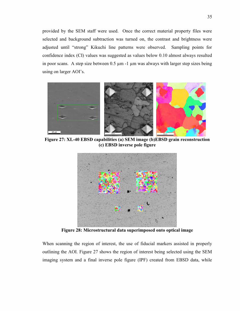
Figure 27: XL-40 EBSD capabilities (a) SEM image (b)EBSD grain reconstruction
(c) EBSD inverse pole figure
Figure 28: Microstructural data superimposed onto optical image
When scanning the region of interest, the use of fiducial markers assisted in properly
outlining the AOI. Figure 27 shows the region of interest being selected using the SEM
imaging system and a final inverse pole figure (IPF) created from EBSD data, while
36
Figure 28 shows the IPF’s of every region on a sample superimposed onto the
corresponding regions.
4.3.4 Gold Nanoparticle Speckle
Following the EBSD scans of all the AOI’s, the process for creating a gold nanoparticle
speckle was started. The process could take anywhere from four to ten days, therefore
multiple tests could take weeks to complete. The methodology for creating a suitable DIC
speckle pattern using gold nanoparticles was introduced by Kammers and Daly [18] to
investigate microstructural phenomena during loading.
The idea behind the gold nanoparticle speckling method is that hydroxide groups that are
commonly found on the surface of metals are increased through solution treatments.
Functionalized silane molecules attach to these added oxide groups and serve as a linker
molecule between the hydroxide groups and the high contrast gold nanoparticles which
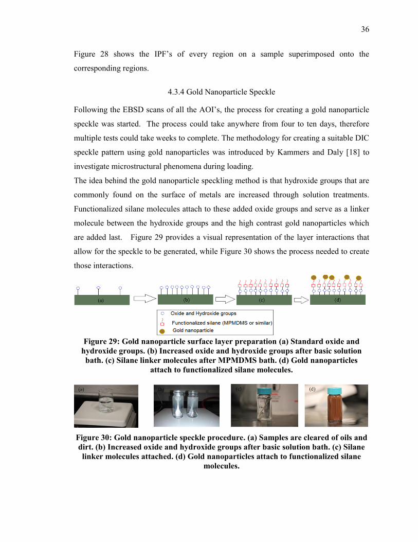
are added last. Figure 29 provides a visual representation of the layer interactions that
allow for the speckle to be generated, while Figure 30 shows the process needed to create
those interactions.
Figure 29: Gold nanoparticle surface layer preparation (a) Standard oxide and
hydroxide groups. (b) Increased oxide and hydroxide groups after basic solution
bath. (c) Silane linker molecules after MPMDMS bath. (d) Gold nanoparticles
attach to functionalized silane molecules.
Figure 30: Gold nanoparticle speckle procedure. (a) Samples are cleared of oils and
dirt. (b) Increased oxide and hydroxide groups after basic solution bath. (c) Silane
linker molecules attached. (d) Gold nanoparticles attach to functionalized silane
molecules.
37
Sodium citrate solution was created using deionized water and trisodium citrate
dehydrate (C6H5Na3O7 •2H2O). Gold chloride solution was created using gold (III)
chloride trihydrate (HAuCl4•3H2O) and deionized water. Adding citrate solution to the
gold chloride solution reduced the size of the gold particles. If larger gold particles were
needed, less citrate was added. The gold nanoparticles synthesized for this work were
smaller than 100nm in diameter. It was discovered that smaller particles naturally take
longer to densely cover the surface of a specimen. As a result, the time samples were to
sit in gold nanoparticle solution was adjusted according to size of gold nanoparticles.
Larger particles on the order of 500nm required the suggested one day incubation period
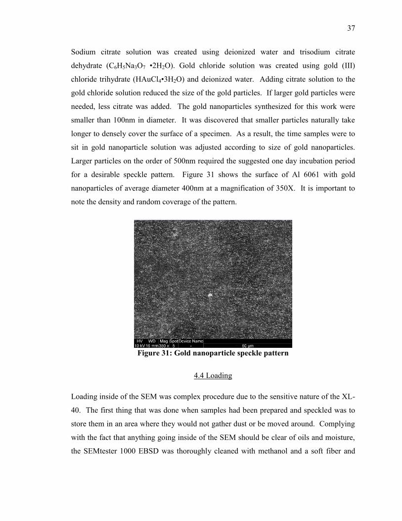
for a desirable speckle pattern. Figure 31 shows the surface of Al 6061 with gold
nanoparticles of average diameter 400nm at a magnification of 350X. It is important to
note the density and random coverage of the pattern.
Figure 31: Gold nanoparticle speckle pattern
4.4 Loading
Loading inside of the SEM was complex procedure due to the sensitive nature of the XL-
40. The first thing that was done when samples had been prepared and speckled was to
store them in an area where they would not gather dust or be moved around. Complying
with the fact that anything going inside of the SEM should be clear of oils and moisture,
the SEMtester 1000 EBSD was thoroughly cleaned with methanol and a soft fiber and

38
cotton swabs. This cleaning was applied to the wiring leading to the port cover, as well
as the inside of the port cover.
The tensile tester was fitted with the manufactured stage mounts and carefully placed
inside of the XL-40. It was crucial that no component of the tester made contact with
anything other than the stage on which it sat on. Cleaned cable ties were used to prevent
dangling wires from coming into contact with anything else as it would trigger a safety
switch within the machine. The microscope software was used to move the stage to
ensure no touch sensors were triggered.
Since a high vacuum was required for operation, proper fitting of the port covers was
crucial. Failure to properly secure the port cover could have led to failure of the XL-40
entirely. The O-ring section of the port cover was carefully matched over the
corresponding groove on the XL-40 and alternating screws were tightened. Figure 32
shows the SEMtester resting on the stage with the modified port cover properly placed.
Figure 32: Modified port cover on XL-40
For reasons explained in Chapter 6, vibrations and load instability prevented the
acquisition of images while being stressed, as was done in Chapter 3. Instead, the Al
6061 sample was displaced to 3.5mm and then returned to 0 MPa stress. This was done
to create some residual stresses and plastic deformations that would be tracked using
DIC. The loading profile is shown below in Figure 33.

39
Figure 33: Loading profile executing inside of the XL-40
4.5 Image Acquisition
Upon viewing the gold nanoparticle speckle pattern in the XL-40 it was believed that
large gold particles were too sparse and would not provide the level of detail sought after.
However, closer inspection revealed that nanoparticles less than 100 nanometers in
diameter were tightly packed across the entirety of the surface. Due to the fact that
individual nanoparticles could be distinguished, albeit difficult due to a moiré pattern
created, the speckle was deemed appropriate.
Due to the very small size of the speckle particles, a magnification of 5000X had to be
used to obtain a roughly 4 x 4 pixel/speckle ratio. This however created a very small
field of view of 24.79 x 18.6 µm. In order to obtain meaningful correlation results,
various grains had to be studied. Manual stitching was the only way to investigate the
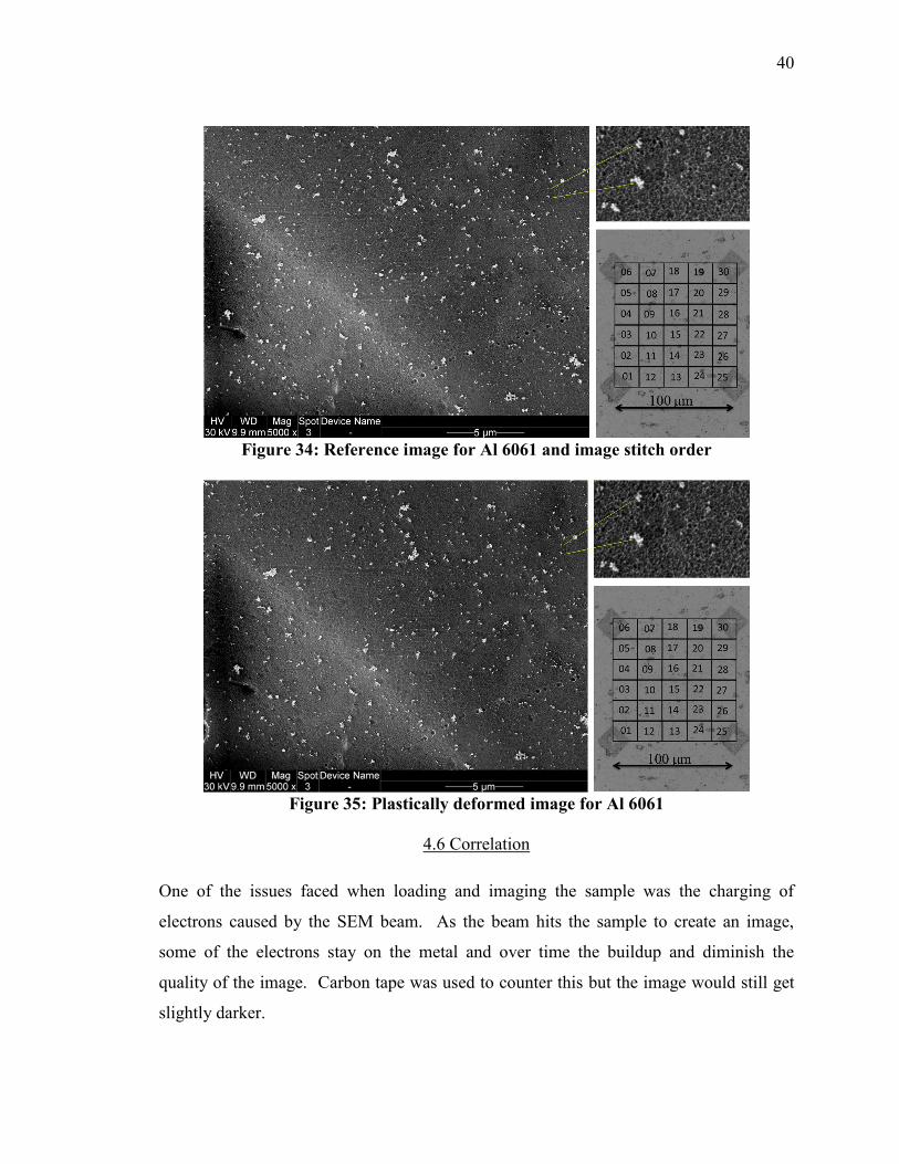
100 µm x 100 µm AOI. Figure 34 and Figure 35 show the first of 25 images used to
stitch a complete region. As shown in the images, a working distance of about 10mm
was used with an accelerating voltage of 30 kV and an aperture lens 3. An overlap of
around 10% was selected to save time and ensure proper image matching in the stitching
process. The stage had difficulty moving in increments of 1-2 µm and as a result, it was
difficult to image the exact same frame for the before and after images, as shown below.
Stress vs. Strain – Al 6061
40
Figure 34: Reference image for Al 6061 and image stitch order
Figure 35: Plastically deformed image for Al 6061
4.6 Correlation
One of the issues faced when loading and imaging the sample was the charging of
electrons caused by the SEM beam. As the beam hits the sample to create an image,
some of the electrons stay on the metal and over time the buildup and diminish the
quality of the image. Carbon tape was used to counter this but the image would still get
slightly darker.
41
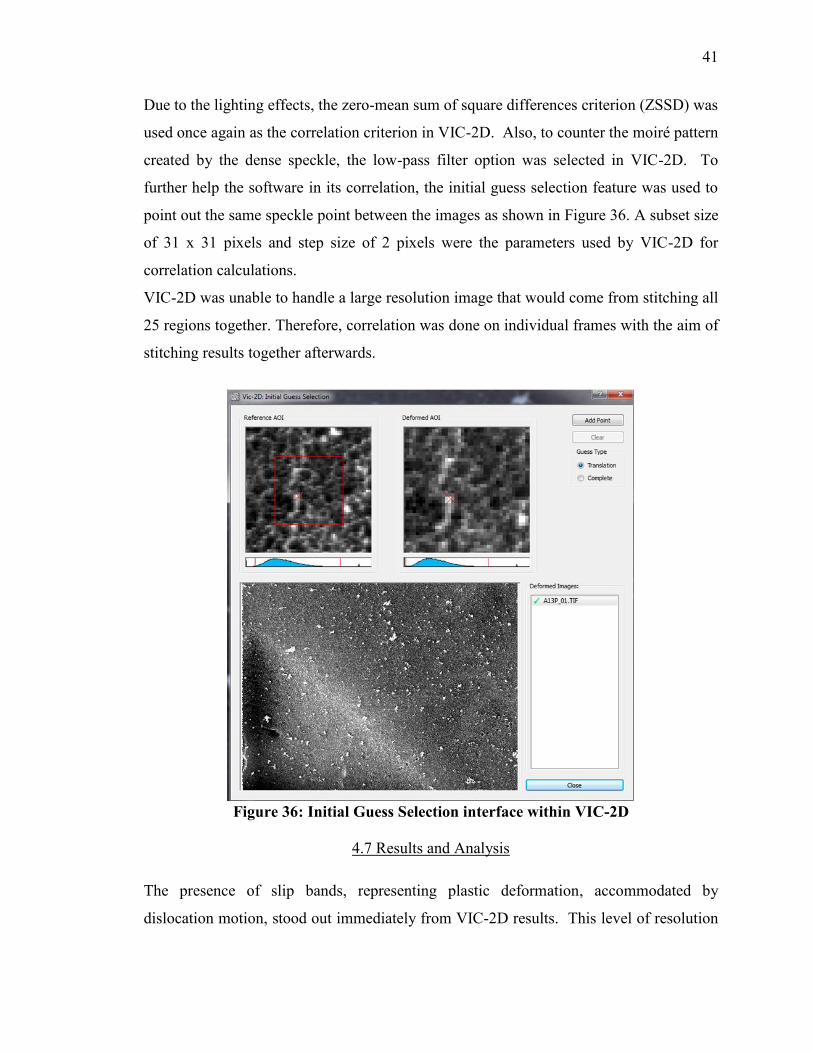
Due to the lighting effects, the zero-mean sum of square differences criterion (ZSSD) was
used once again as the correlation criterion in VIC-2D. Also, to counter the moiré pattern
created by the dense speckle, the low-pass filter option was selected in VIC-2D. To
further help the software in its correlation, the initial guess selection feature was used to
point out the same speckle point between the images as shown in Figure 36. A subset size
of 31 x 31 pixels and step size of 2 pixels were the parameters used by VIC-2D for
correlation calculations.
VIC-2D was unable to handle a large resolution image that would come from stitching all
25 regions together. Therefore, correlation was done on individual frames with the aim of
stitching results together afterwards.
Figure 36: Initial Guess Selection interface within VIC-2D
4.7 Results and Analysis
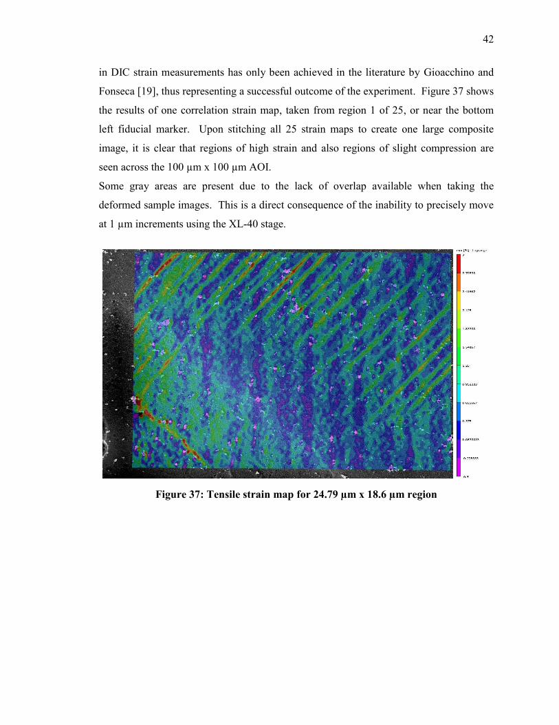
The presence of slip bands, representing plastic deformation, accommodated by
dislocation motion, stood out immediately from VIC-2D results. This level of resolution
42
in DIC strain measurements has only been achieved in the literature by Gioacchino and
Fonseca [19], thus representing a successful outcome of the experiment. Figure 37 shows
the results of one correlation strain map, taken from region 1 of 25, or near the bottom
left fiducial marker. Upon stitching all 25 strain maps to create one large composite
image, it is clear that regions of high strain and also regions of slight compression are
seen across the 100 µm x 100 µm AOI.
Some gray areas are present due to the lack of overlap available when taking the
deformed sample images. This is a direct consequence of the inability to precisely move
at 1 µm increments using the XL-40 stage.
Figure 37: Tensile strain map for 24.79 µm x 18.6 µm region
43
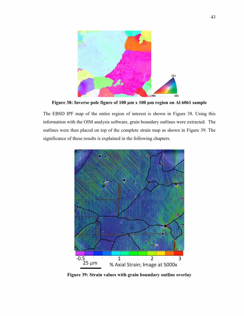
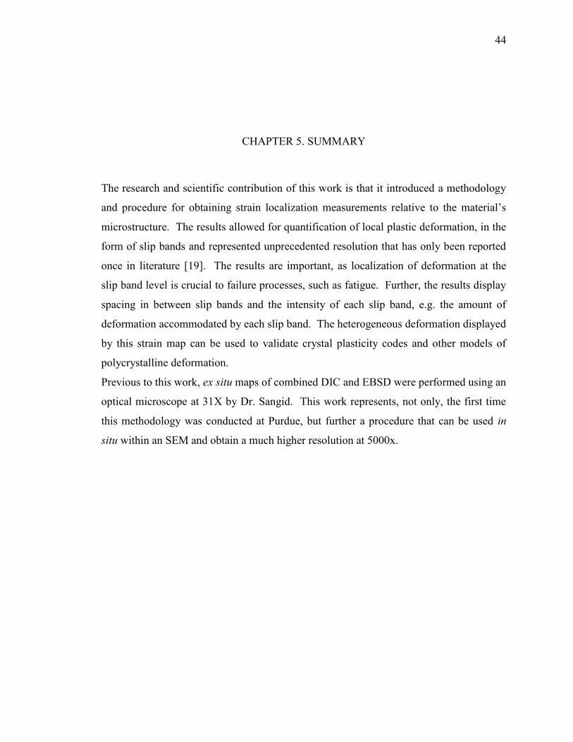
Figure 38: Inverse pole figure of 100 µm x 100 µm region on Al 6061 sample
The EBSD IPF map of the entire region of interest is shown in Figure 38. Using this
information with the OIM analysis software, grain boundary outlines were extracted. The
outlines were then placed on top of the complete strain map as shown in Figure 39. The
significance of these results is explained in the following chapters.
Figure 39: Strain values with grain boundary outline overlay
44
CHAPTER 5. SUMMARY
The research and scientific contribution of this work is that it introduced a methodology
and procedure for obtaining strain localization measurements relative to the material’s
microstructure. The results allowed for quantification of local plastic deformation, in the
form of slip bands and represented unprecedented resolution that has only been reported
once in literature [19]. The results are important, as localization of deformation at the
slip band level is crucial to failure processes, such as fatigue. Further, the results display
spacing in between slip bands and the intensity of each slip band, e.g. the amount of
deformation accommodated by each slip band. The heterogeneous deformation displayed
by this strain map can be used to validate crystal plasticity codes and other models of
polycrystalline deformation.
Previous to this work, ex situ maps of combined DIC and EBSD were performed using an
optical microscope at 31X by Dr. Sangid. This work represents, not only, the first time
this methodology was conducted at Purdue, but further a procedure that can be used in
situ within an SEM and obtain a much higher resolution at 5000x.
45
CHAPTER 6. RECOMMENDATIONS AND FUTURE WORK
6.1 Overview
The use of DIC in combination with microstructure information from EBSD represents a
promising avenue for understanding strain localization and the role of defects on
deformation. Based on this work, the following recommendations and future work are
outlined. Recommendations are split into (i) improvements to speckle pattern, (ii)
technical problems with the MTI load frame, (iii) addressing bias in DIC reported strain
maps, and (iv) slip system quantification of plastic strain. Further, future work is
outlined.
6.2 Recommendations
6.2.1 Future Speckle
Currently, the ACME laboratory has an Allied Vision Technologies Manta camera with
3.4X, 10X, and 20X lenses to perform DIC experiments using the MTS Hydraulic load
frames. It was attempted to use the silicon oxide speckle to study fatigue crack growth,
but unsatisfactory results were produced. This was more than likely attributed to the
vibrations induced by the machine and the building along with the out of plane
misalignment. Applying the silicon oxide speckle to a simple tensile test and producing
results that complement test data, as was done in this work, proves that DIC experiments
can be reliably conducted at around 10X, with 1.5 µm silicon particles, when out of plane
misalignments are not an issue. With crack propagation tips measuring from anywhere
around 1 µm – 10 µm, 1.5 µm silicon particles may be too large to study localized stress
at a crack tip. However, the silicon oxide speckle method is time and cost efficient,
making it a must have technique for larger scale projects.

46
The gold nanoparticles synthesized in this work were on the order of 10 nm-100 nm,
which makes it impossible to track with the Olympus microscope unless large clumps are
present. In order to perform optical DIC strain measurements with high levels of detail,
gold nanoparticles should be synthesize to have a size of around 200 nm – 400 nm. This
will allow the Olympus microscope at 100X to reach an ideal ratio of around 3 x 3 pixels
per particle.
6.2.2 Load Frame Issues
The following recommendations have been developed to ensure smooth operation of the
machinery. These recommendations have been communicated with the manufacturer,
MTI, and are being addressed.
1. Reliable load-displacement curve (correct load frame compliance and slipping of
grips). For this load frame to be usable, the load frame should show evidence of
repeatable load-displacement curves for similar materials/samples at room and
elevated temperature. From experience (even at room temperature), the load
frame does not produce reliable results. Four Al 6061 samples were stressed until
failure and gave the responses shown below in Figure 40.
Figure 40: Stress-strain curve of Al 6061

47
2. Bending stress cannot be induced on the sample. That is the loading axis needs to
be aligned to the sample’s major axis, which will require a redesign of the grips.
Data should confirm the specimen is in a uni-axial tensile stress state and is free
of bending (in compliance with ASTM E04).
3. As reported, the load frame experiences incipient heating. So, either the grips
need to be cooled or sufficient insulation needs to be placed between the grips and
load cell to ensure that it is safe and reliable to test at elevated temperatures. The
load frame needs to ensure that while the specimen is heated to elevated
temperatures, the load cell and linear variable differential transformer are within
their certified operation temperature range as indicated by the original equipment
manufacturer.
4. Upgrade the wiring and connectors in the system and replace the motor to the
linearize motor, to ensure it does not overheat during testing. The wiring and
connectors are rated for internal computer components and are not designed to
operate in a lab environment that requires handling.
6.2.3 SEM-DIC Bias
As reported by Kammers and Daly [40], the high spatial resolution of DIC imaged
through an SEM enables aliasing and thereby complex image distortions, as shown in
Figure 41. Further, the long acquisition time during image collection can result in stress
relaxation. Additionally, specific to the SEM, high noise sensitivity must be accounted
for. Kammers and Daly [40] provided a framework to account for these distortions, thus
improving the quantification accuracy of the DIC method within the SEM. It is
recommended that due to the electromagnetic forces and incipient heating, the distortion
in the resulting strain images must be calibrated.

48
Figure 41: Kammers and Daly, Experimental Mechanics, 53 (2013)
6.2.4 Crystallographic Analysis
To confirm that the strain maps produce by DIC are in fact displaying real phenomenon,
the {111} slip planes that accommodate slip in face centered cubic (fcc) materials should
be projected onto the crystallographic directions of each grain. This will confirm that the
slip bands observed in Figure 39 are not an artifact of the experiment and represent real
materials behavior. Similarly, a quantitative study of local deformation in the vicinity of
microstructure features can be performed [34], which is used to determine the active slip
systems using the measured macroscopic plastic strains and crystal orientation to solve
for the crystallographic shear strains:
Where is the slip system number, s is the number of slip systems (12 for fcc), n is the
vector defining the normal to slip plane for system , l is the vector defining the slip
direction, and d is the shear strain increment for system . Solving for the scalar
quantities d at each spatial point yields local information about slip system activation
across the selected region.
deijp =
1
2ni
a l ja + n j
a lia( )
a=1
s
å dga = mija( )
a=1
s
å dga

49
From this powerful experimental setup, the following is recommended for future work.
Perform monotonic tests at room and elevated temperatures, to quantify the
heterogeneous nature of polycrystalline deformation. Further, the experimental
results can provide the same input to crystal plasticity simulations, to validate
the model predictions.
The experimental procedure can be used to investigate fatigue. Cyclic loading
can be performed and the strain maps can be obtained during interrupted load
cycles, in order to characterize strain accumulation and quantify the unique
deformation patterns associated with fatigue.
Finally, the microstructure features that promote or resist plastic deformation can
be elucidated, as this information is important to design alloys with increased
performance.
6.3 Future Work
From this powerful experimental setup, the following is recommended for future work.
Perform monotonic tests at room and elevated temperatures, to quantify the
heterogeneous nature of polycrystalline deformation. Further, the experimental
results can provide the same input to crystal plasticity simulations, to validate
the model predictions.
The experimental procedure can be used to investigate fatigue. Cyclic loading
can be performed and the strain maps can be obtained during interrupted load
cycles, in order to characterize strain accumulation and quantify the unique
deformation patterns associated with fatigue.
Finally, the microstructure features that promote or resist plastic deformation can
be elucidated, as this information is important to design alloys with increased
performance.

BIBLIOGRAPHY
50
BIBLIOGRAPHY
[1] Center for Photogrammetric Training, "History of Photogrammetry," 24 August
2008. [Online]. Available:
https://spatial.curtin.edu.au/local/docs/HistoryOfPhotogrammetry.pdf.
[2] A. Rosenfeld, "From Image Analysis to Computer Vision: An Annotated
Bibliography, 1955-1979," Computer Vision and Image Understanding, vol. 84, pp.
298-324, 2001.
[3] W. Peters and W. Ranson, "Digital imaging techniques in experimental stress
analysis," Optical Engineering, vol. 21(3), pp. 427-431, 1982.
[4] W. Peters, W. Ranson, M. Sutton, T. Chu and J. Anderson, "Application of digital
image correlation methods to rigid body mechanics," Opt. Eng., vol. 22(6), pp. 738-
742, 1983.
[5] M. Sutton, M. Cheng, W. Peters, Y. Chao and S. McNeill, "Application of an
optimized digital image correlation method to planar deformation analysis," Image
Vision Comput., vol. 4, pp. 143-150, 1986.
[6] M. Sutton, W. Wolters, W. Peters, W. Ranson and S. McNeill, "Determination of
displacements using an improved digital correlation method," Image and Vision
Computing, vol. 1, no. 3, pp. 133-139, 1983.
[7] M. Sutton, J. Orteu and H. Schreier, Image Correlation for Shape, Motion and
Deformation Measurements, New York: Springer Science, 2009.
[8] J. Carrol, Relating Fatigue Crack Growth To Microstructure Via Multiscale Digital
Image Correlation, Ph.D. Thesis, University of Illionois at Urbana-Champaign,
2011.
[9] P. Reu, "Introduction to Digital Image Correlation: Best Practices and Applications,"
Experimental Techniques, vol. 36, no. 1, pp. 3-4, 2012.
[10] T. Chu, W. Ranson, M. Sutton and W. Peters, "Applications of Digital-Image-
Correlation Techniques to Experimental Mechanics," Experimental Mechanics, vol.
25, no. 3, pp. 232-244, 1985.
[11] W. Tong, "Detection of plastic deformation patterns in a binary aluminium alloy,"
Experimental Mechanics, vol. 37, pp. 452-459, 1997.
[12] N. Zhang and W. Tong, "An experimental study on grain deformation and
interactions in an Al-0.5 % Mg muticrystal," Int J Plast, vol. 20, pp. 523-542, 2004.
[13] J. Dally and W. Riley, Experimental Stress Analysis, New York: McGraw-Hill,
1991.
51
[14] B. Schroeter and D. McDowell, "Measurement of deformation fields in
polycrystaliline OFHC copper," International Journal of Plasticity, vol. 19, pp.
1355-1376, 2003.
[15] J. Walley, R. Wheeler, M. Uchic and M. Mills, "In-Situ Mechanical Testing for
Characterizing Strain Localization During Deformation at Elevated Temperatures,"
Experimental Mechanics, vol. 52, pp. 405-416, 2012.
[16] W. Scrivens, Y. Luo, M. Sutton, S. Collette, M. Myrick, P. Miney, P. Colavita, A.
Reynolds and X. Li, "Development of Patterns for Digital Image Correlation
Measurements at Reduced Length Scales," Experimental Mechanics, vol. 47, pp. 63-
77, 2007.
[17] K. Jonnalagadda, I. Chasiiotis, S. Yagnamurthy, J. Lambros, J. Polskamp, R.
Polcawich and M. Dubey, "Experimental Investigation of Strain Rate Dependence of
Nanocrystalline Pt Films," Experimental Mechanics, vol. 50, pp. 25-35, 2010.
[18] A. D. Kammers and S. Daly, "Self-Assembled Nanoparticle Surface Patterning for
Improved Digital Image Correlation in a Scanning Electron Microscope,"
Experimental Mechanics, vol. 53, no. 8, pp. 1333-1341, 2013.
[19] F. Di Gioacchino and J. Quinta da Fonseca, "Plastic Strain Mapping with Sub-
micron Resolution Using Digital Image Correlation," Experimantal Mechanics, vol.
53(5), pp. 743-754, 2013.
[20] M. Sutton, J. Turner, Y. Chao, H. Bruck and T. Chae, "Experimental investigations
of three-dimensional effects near a crack tip using computer vision," International
Journal of Fracture, vol. 53, pp. 201-228, 1992.
[21] M. Sutton, W. Zhao, R. McNeill, J. Helm, R. Piascik and W. Riddell, "Local Crack
Closure Measurements: Development of a Measurement System Using Computer
Vision and a Far-Field Microscope," Advances in Fatigue Crack Closure
Measurement and Analysis, vol. 2, pp. 145-156, 1997.
[22] J. Abanto-Bueno and J. Lambros, "Investigation of crack growth in functionally
graded materials using digital image correlation," Engineering Fracture Mechanics,
vol. 69, pp. 1695-1711, 2002.
[23] J. Chen, N. Zhan, X. Zhang and J. Wang, "Improved extended digital image
correlation for crack tip deformation measurement," Optics and Lasers in
Engineering, 2014.
[24] G. Pataky, M. Sangid, H. Sehitoglu, R. Hamilton, H. Maier and P. Sofronis, "Full
field measurements of anisotropic stress intensity factor ranges in fatigue,"
Engineering Fracture Mechanics, vol. 94, pp. 12-28, 2012.
[25] S. Shah and J. Chandra Kishen, "Fracture Properties of Concrete-Concrete Interfaces
Using Digital Image Correlation," Experimental Mechanics, vol. 51, pp. 303-313,
2011.
[26] B. Justusson, D. Spagnuolo and J. Yu, "Assessing the applicability of digital image
correlation (DIC) technique in tensile testing of fabric composites," Army Research
Laboratory, Aberdeen Proving Ground, MD, 2013.

52
[27] Y. He, A. Makeev and B. Shonkwiler, "Characterization of nonlinear shear
properties for composite materials using digital image correlation and finite element
analysis," Composites Science and Technology, vol. 73, pp. 64-71, 2012.
[28] M. Caminero, M. Lopez-Pedrosa, C. Pinna and C. Soutis, "Damage Assessment of
Composite Structures Using Digital Image Correlation," Applied Composite
Materials, vol. 21, pp. 91-106, 2014.
[29] S. Pavel, M. Vanleene, R. Olsson, R. Collinson, A. Pitsillides and S. Shefelbine,
"Using digital image correlation to determine bone surface strains during loading
and after adaption of the mouse tibia," Journal Biomechanics, vol. 43, pp. 599-605,
2010.
[30] S. Väänänen, S. Yavari, H. Weinans, A. Zadpoor, J. Jurvelin and H. Isaksson,
"Repeatability of digital image correlation for measurement of surface strains in
composite long bones," Journal of Biomechanics, vol. 46, pp. 1928-1932, 2013.
[31] N. Miura, S. Arikawa, S. Yoneyama, M. Koike, M. Murakami and O. Tanno,
"Digital Image Correlation Strain Analysis for the Study of Wrinkle Formation on
Facial Skin," Journal of Solid Mechanics and Materials Engineering, vol. 6, no. 6,
pp. 545-554, 2012.
[32] M. Tschopp, B. Bartha, W. Porter, P. Murray and S. Fairchild, "Microstructure-
Dependent Local Strain Behavior in Polycrystals through In-Situ Scanning Electron
Microscope Tensile Experiments," Metallurgical and Materials Transactions A, vol.
40, no. 10, pp. 2363-2368, 2009.
[33] A. Clair, M. Foucault, O. Calonne, Y. Lacroute, L. Markey, M. Salazar, V. Vignal
and E. Finot, "Strain mapping near a triple junction in strained Ni-based alloy using
EBSD and biaxial nanogauges," Acta Materialia, vol. 59, no. 8, pp. 3116-3123,
2011.
[34] W. Abuziad, M. Sangid, J. Carroll, H. Sehitoglu and J. Lambros, "Slip transfer and
plastic strain accumulation across grain boundaries," Journal of the Mechanics and
Physics of Solids, vol. 60, pp. 1201-1220, 2012.
[35] J. L. Carter, N. Zhou, J. Sosa, P. Shade, A. Pilchak, M. W. Kuper, Y. Wang, M. D.
Uchic, M. J. Mills and H. Fraser, "Characterization of Strain Accumulation at Grain
Boundaries of NickelBased Superalloys," in Superalloys 2012, TMS: Champion,
PA, 2012.
[36] T. Turner, P. Shade, J. Schuren and M. Groeber, "The influence of microstructure on
surface strain distributions in a nickel micro-tension specimen," Modelling and
Simulation in Materials Science and Engineering, vol. 21, no. 1, 2013.
[37] D. C. Zipperian, Pace Technologies Metallographic Handbook, Tucson, AZ: PACE
Technologies, 2011.
[38] B. Puccio, "AAE 490 Speckle pattern Procedure," School of Aeronautics and
Astronautics, Purdue University, 2013.
[39] H. Schreier, J. Braasch and M. Sutton, "Systematic errors in digital image
correlation caused by intensity interpolation," Optical Engineering, vol. 39, p. 2915,
2000.

53
[40] A. Kammers and S. Daly, "Digital Image Correlation under Scanning Electron
Microscopy: Methodology and Validation," Experimental Mechanics, vol. 53, pp.
1743-1761, 2013.
[41] G. Parada and M. Sangid, "Set-up of Digital Image Correlation Apparatus," The
Summer Undergraduate Research Fellowship (SURF), 2013.

APPENDIX

54
AP
PE
ND
IX:
SP
EC
IME
N P
AR
T D
RA
WIN
G