Embed Size (px)
Citation preview
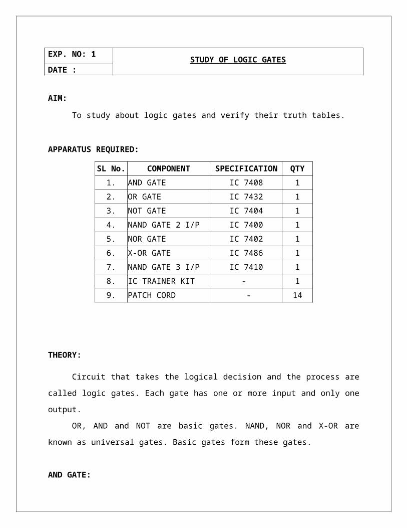
EXP. NO: 1STUDY OF LOGIC GATES
DATE :
AIM:
To study about logic gates and verify their truth tables.
APPARATUS REQUIRED:
THEORY:
Circuit that takes the logical decision and the process are called logic gates. Each gate has
one or more input and only one output.
OR, AND and NOT are basic gates. NAND, NOR and X-OR are known as universal
gates. Basic gates form these gates.
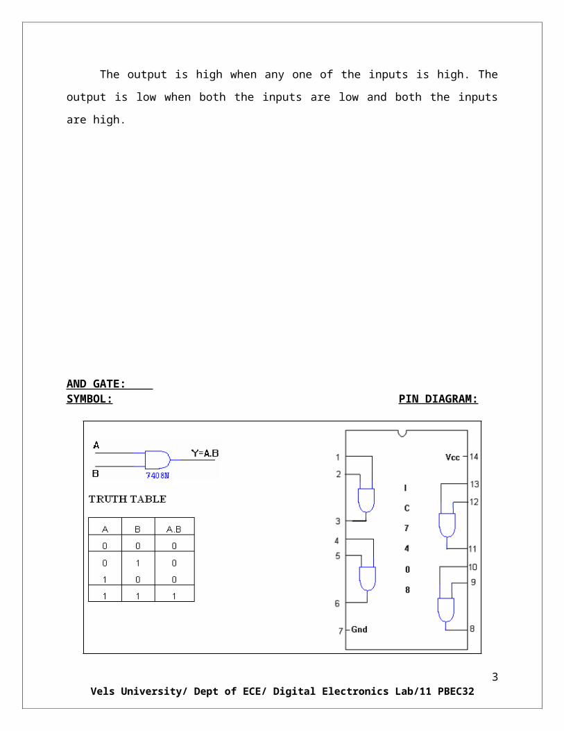
AND GATE:
The AND gate performs a logical multiplication commonly known as AND function. The
output is high when both the inputs are high. The output is low level when any one of the inputs
is low.
SL No. COMPONENT SPECIFICATION QTY
1. AND GATE IC 7408 1
2. OR GATE IC 7432 1
3. NOT GATE IC 7404 1
4. NAND GATE 2 I/P IC 7400 1
5. NOR GATE IC 7402 1
6. X-OR GATE IC 7486 1
7. NAND GATE 3 I/P IC 7410 1
8. IC TRAINER KIT - 1
9. PATCH CORD - 14
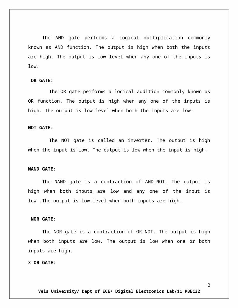
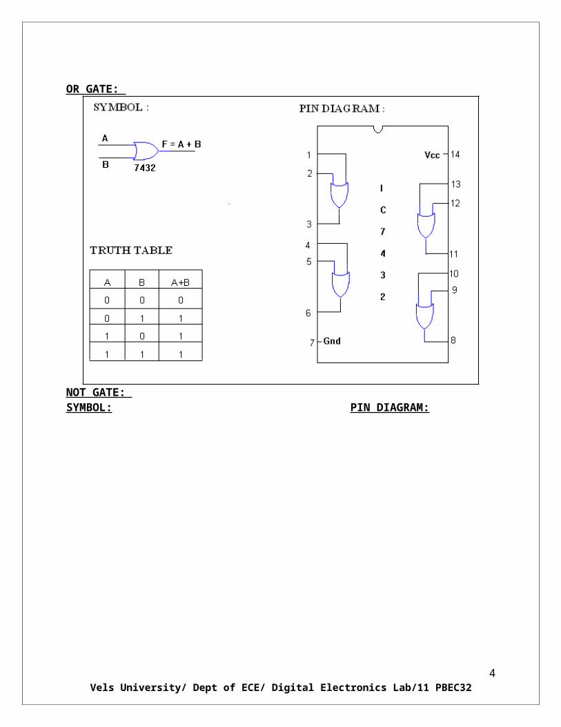
OR GATE:
The OR gate performs a logical addition commonly known as OR function. The
output is high when any one of the inputs is high. The output is low level when both the inputs
are low.
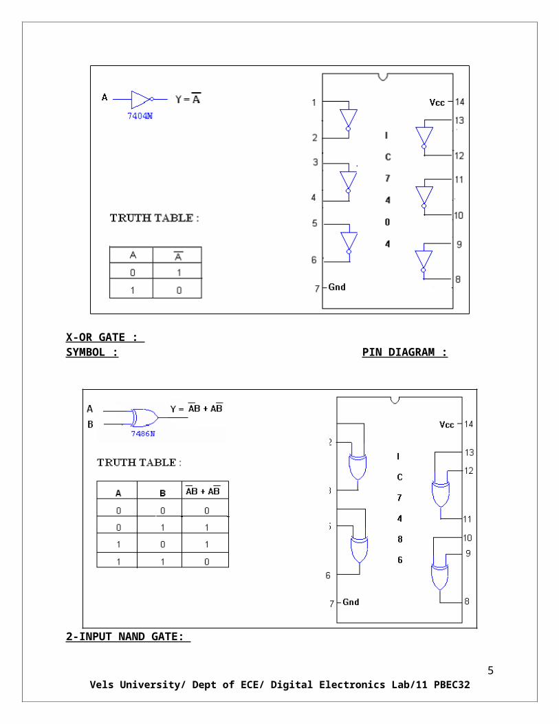
NOT GATE:
The NOT gate is called an inverter. The output is high when the input is low. The
output is low when the input is high.
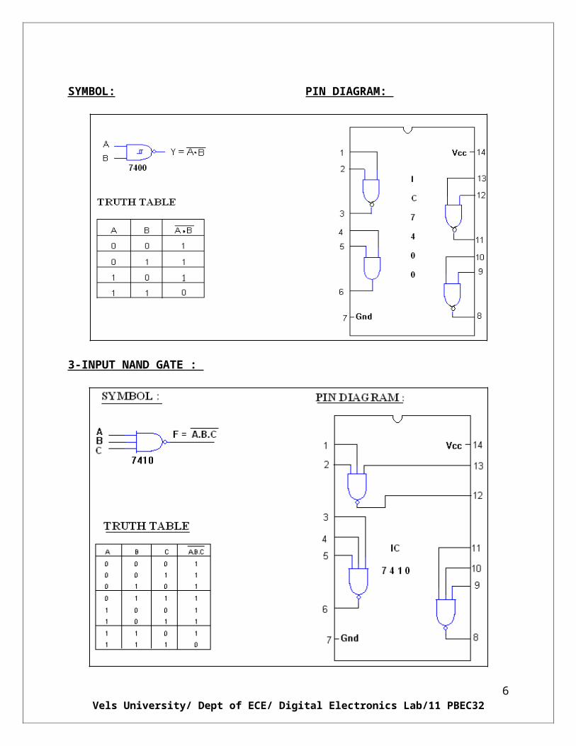
NAND GATE:
The NAND gate is a contraction of AND-NOT. The output is high when both inputs are
low and any one of the input is low .The output is low level when both inputs are high.
NOR GATE:
The NOR gate is a contraction of OR-NOT. The output is high when both inputs are low.
The output is low when one or both inputs are high.
X-OR GATE:
The output is high when any one of the inputs is high. The output is low when both the
inputs are low and both the inputs are high.
2Vels University/ Dept of ECE/ Digital Electronics Lab/11 PBEC32
AND GATE: SYMBOL: PIN DIAGRAM:
OR GATE:
3Vels University/ Dept of ECE/ Digital Electronics Lab/11 PBEC32
NOT GATE: SYMBOL: PIN DIAGRAM:
X-OR GATE : SYMBOL : PIN DIAGRAM :
2-INPUT NAND GATE:
4Vels University/ Dept of ECE/ Digital Electronics Lab/11 PBEC32
SYMBOL: PIN DIAGRAM:
3-INPUT NAND GATE :
NOR GATE:
5Vels University/ Dept of ECE/ Digital Electronics Lab/11 PBEC32
6Vels University/ Dept of ECE/ Digital Electronics Lab/11 PBEC32
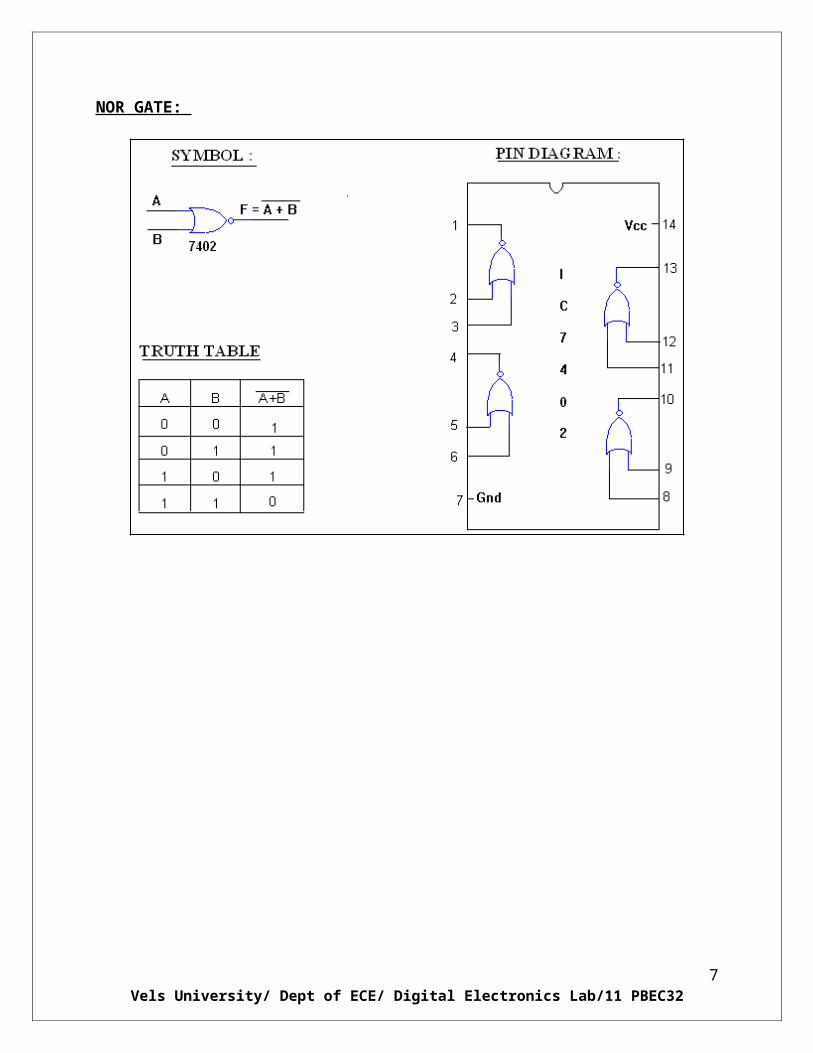
PROCEDURE:
a. Give connections as per the circuit diagramb. Inputs are given to the circuit making high ‘1’ i.e. +5 V or + Vcc supply to the
14th pin and for low ‘0’ i.e. GND to the 7th pin of the gate ICc. Depending upon the truth table, if the LED glow it represent 1 and else it
represents ‘0’d. Verify the truth table as given e. Repeat the procedure steps for different gates.
RESULT: Thus the truth tables for logic gates are verified using IC trainer kit.
7Vels University/ Dept of ECE/ Digital Electronics Lab/11 PBEC32
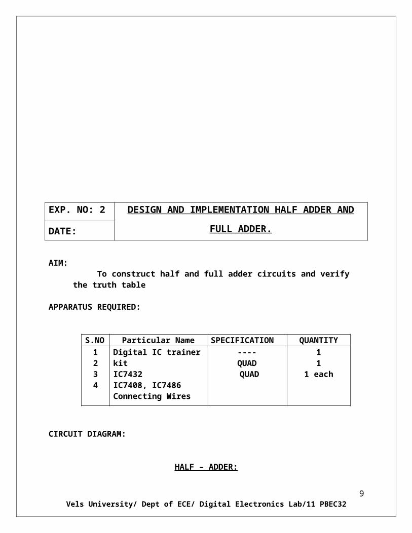
EXP. NO: 2 DESIGN AND IMPLEMENTATION HALF ADDER AND
FULL ADDER.DATE:
AIM: To construct half and full adder circuits and verify the truth table
APPARATUS REQUIRED:
S.NO Particular Name SPECIFICATION QUANTITY
1234
Digital IC trainer kitIC7432 IC7408, IC7486Connecting Wires
----QUAD QUAD
11
1 each
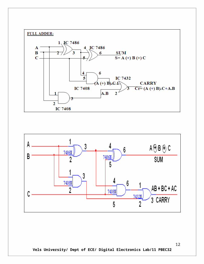
CIRCUIT DIAGRAM:
HALF – ADDER:
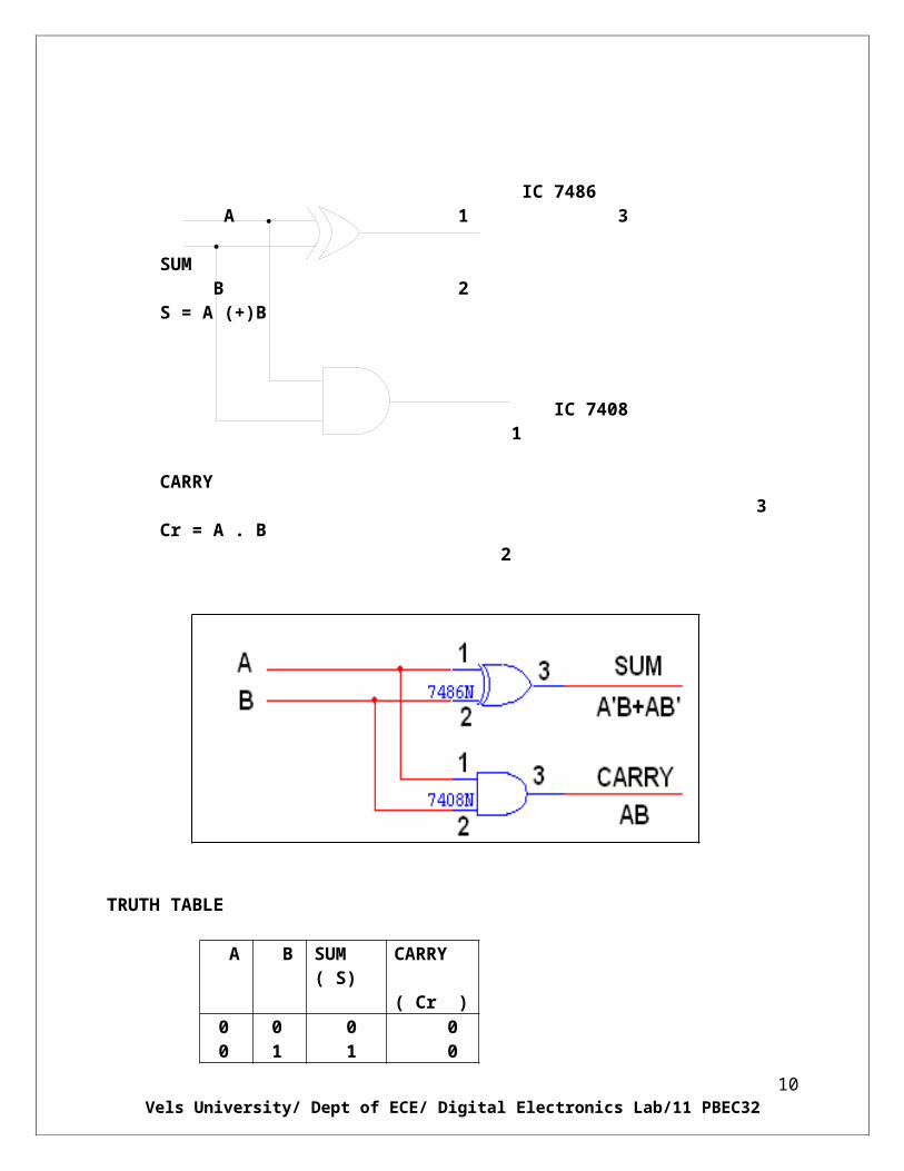
IC 7486 A 1 3 SUM B 2 S = A (+)B
IC 7408 1 CARRY 3 Cr = A . B 2
8Vels University/ Dept of ECE/ Digital Electronics Lab/11 PBEC32
TRUTH TABLE
A B SUM ( S)
CARRY ( Cr )
0 0 1 1
0 1 0 1
0 1 1 0
0 0 0 1
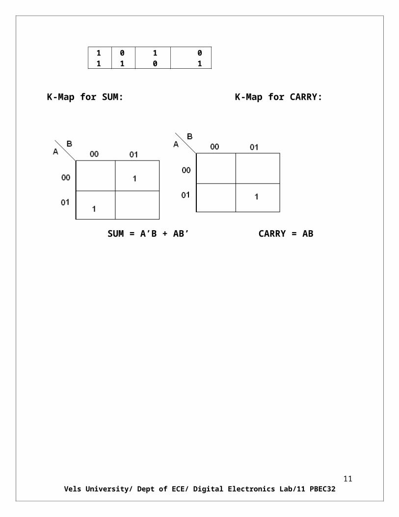
K-Map for SUM: K-Map for CARRY:
SUM = A’B + AB’ CARRY = AB
9Vels University/ Dept of ECE/ Digital Electronics Lab/11 PBEC32
10Vels University/ Dept of ECE/ Digital Electronics Lab/11 PBEC32
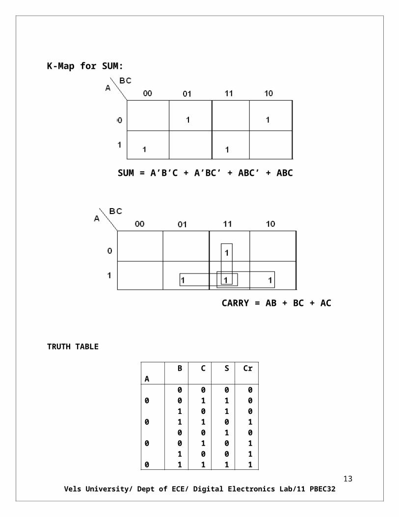
K-Map for SUM:
SUM = A’B’C + A’BC’ + ABC’ + ABC
CARRY = AB + BC + AC
TRUTH TABLE
A B C S Cr 0 0 0 0 1 1 1 1
0 0 1 1 0 0 1 1
0 1 0 1 0 1 0 1
0 1 1 0 1 0 0 1
0 0 0 1 0 1 1 1
11Vels University/ Dept of ECE/ Digital Electronics Lab/11 PBEC32
PROCEDURE:
1. Give connections as per the circuit diagram
2. Inputs are given to the circuit making high ‘1’ i.e. +5 V or
+ Vcc supply to the 14th pin and for low ‘0’ i.e. GND to the 7th
pin of the gate IC
3. Depending upon the truth table, if the LED glow it represent 1 and else it represents ‘0’
4. Verify the truth table as given for half adder
5. Repeat the procedure steps for full adder circuit
RESULT:
The half and full adder circuits are constructed and verified.
12Vels University/ Dept of ECE/ Digital Electronics Lab/11 PBEC32
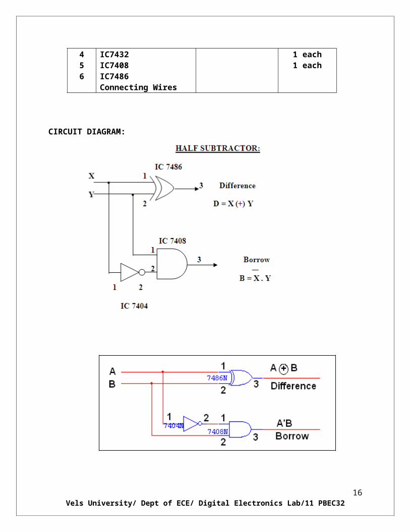
EXP. NO: 3DESIGN AND IMPLEMENTATION OF SUBTRACTORS
USING LOGIC GATESDATE:
AIM:
To construct half and full subtractor circuits and verify the truth table
APPARATUS REQUIRED:
S.NO Particular Name SPECIFICATION QUANTITY
1 2 3 4 5 6
Digital IC trainer kitIC7404IC7432 IC7408IC7486Connecting Wires
---- 11 each1 each1 each1 each
CIRCUIT DIAGRAM:
13Vels University/ Dept of ECE/ Digital Electronics Lab/11 PBEC32
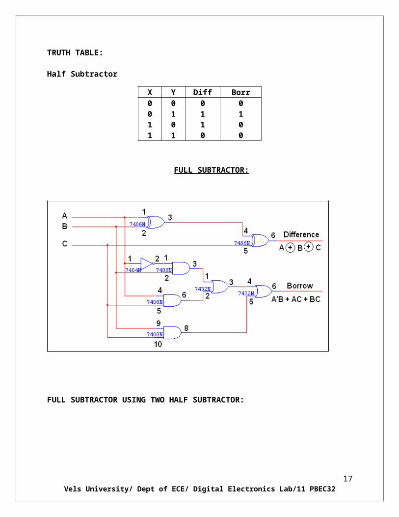
TRUTH TABLE:
Half Subtractor
FULL SUBTRACTOR:
14Vels University/ Dept of ECE/ Digital Electronics Lab/11 PBEC32
X Y Diff Borr0011
0101
0110
0100

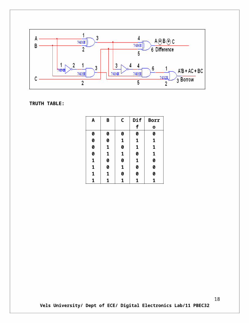
FULL SUBTRACTOR USING TWO HALF SUBTRACTOR:
TRUTH TABLE:
15Vels University/ Dept of ECE/ Digital Electronics Lab/11 PBEC32
A B C Diff Borro00001111
00110011
01010101
01101001
0111000 1
PROCEDURE: 1. Give connections as per the circuit diagram
2. Inputs are given to the circuit making high ‘1’ i.e. +5 V or + Vcc supply to the 14th
pin and for low ‘0’ i.e. GND to the 7th pin of the gate IC
3. Depending upon the truth table, if the LED glow it represent 1 and else it represents
‘0’
4. Verify the truth table as given for half subtractor
5. Repeat the procedure steps for full subtractor circuits
RESULT:
The half and full subtractor circuits are constructed and truth table was verified
16Vels University/ Dept of ECE/ Digital Electronics Lab/11 PBEC32
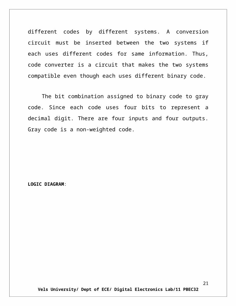
EXP. NO: 4BINARY TO GRAY - CODE CONVERTER
DATE:AIM:
To Construct and Verify the Truth Table of Binary to Gray Code Converter.
APPARATUS REQUIRED:
S.NO Particular Name SPECIFICATION QUANTITY
123
Digital IC trainer kitIC 7486Connecting Wires
----QUADQUAD
131
THEORY:
The availability of large variety of codes for the same discrete elements of
information results in the use of different codes by different systems. A conversion
circuit must be inserted between the two systems if each uses different codes for
same information. Thus, code converter is a circuit that makes the two systems
compatible even though each uses different binary code.
The bit combination assigned to binary code to gray code. Since each code
uses four bits to represent a decimal digit. There are four inputs and four outputs.
Gray code is a non-weighted code.
17Vels University/ Dept of ECE/ Digital Electronics Lab/11 PBEC32
LOGIC DIAGRAM:
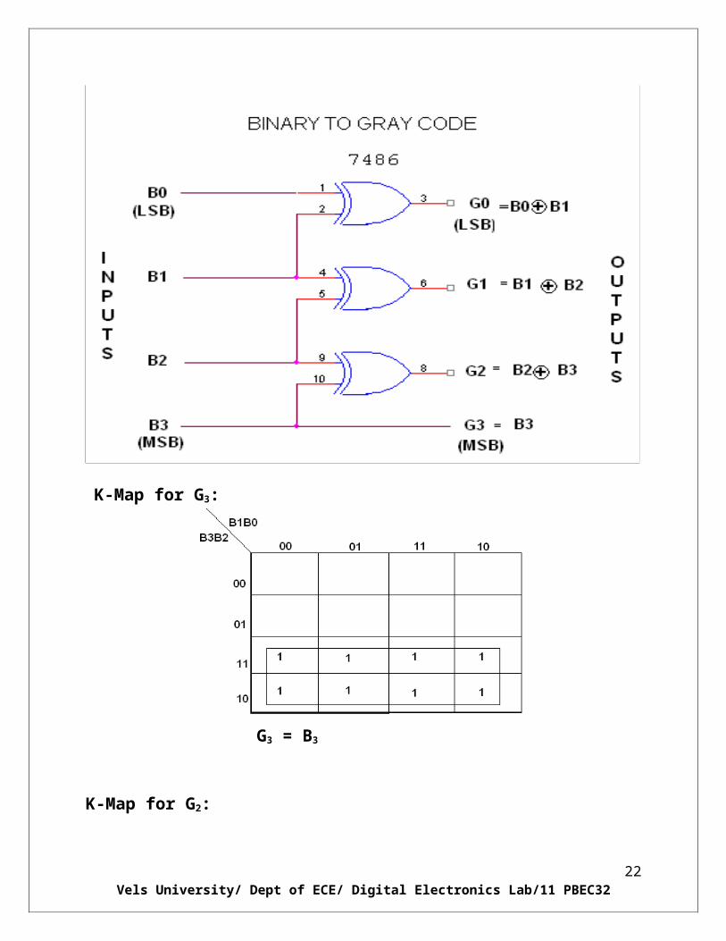
K-Map for G3:
G3 = B3
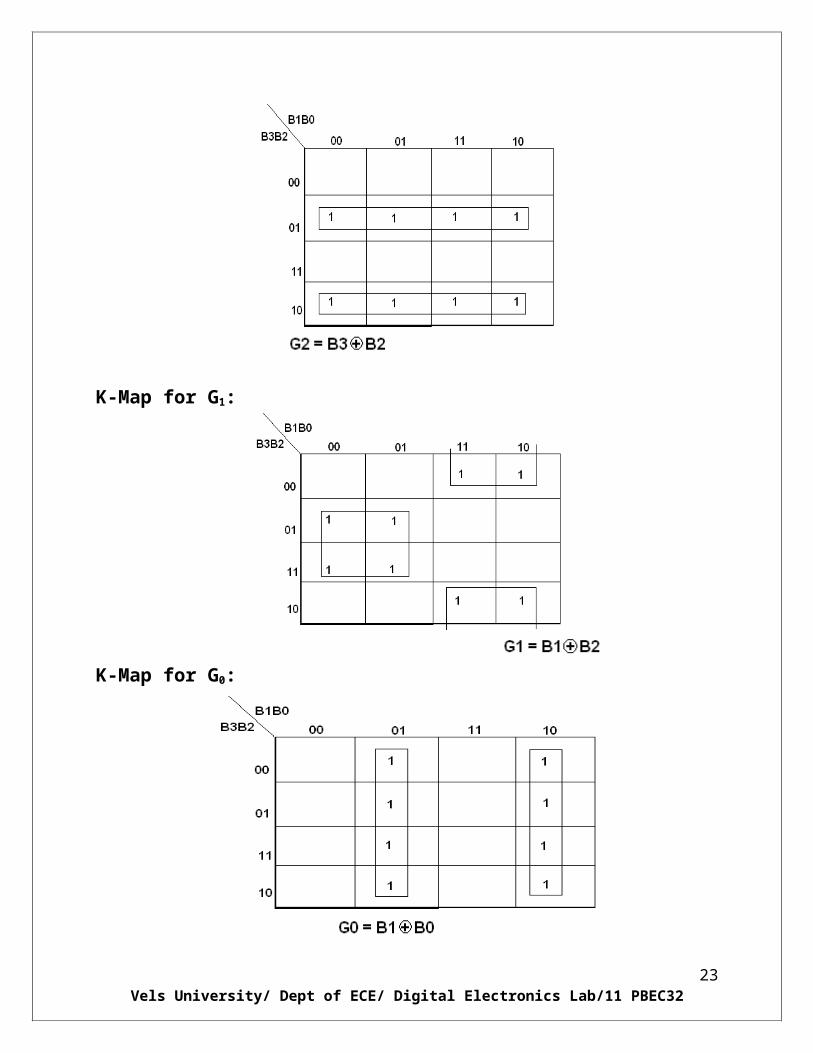
K-Map for G2:
18Vels University/ Dept of ECE/ Digital Electronics Lab/11 PBEC32

K-Map for G1:
K-Map for G0:
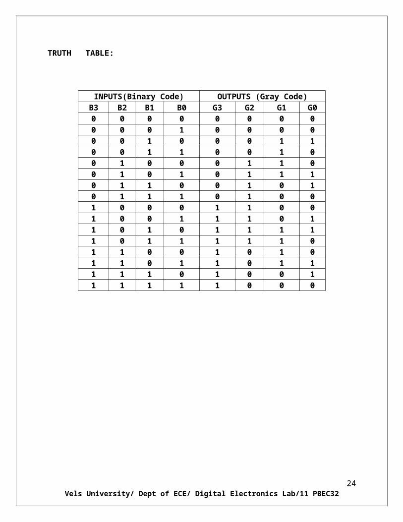
TRUTH TABLE:
19Vels University/ Dept of ECE/ Digital Electronics Lab/11 PBEC32
INPUTS(Binary Code) OUTPUTS (Gray Code)
B3 B2 B1 B0 G3 G2 G1 G00 0 0 0 0 0 0 00 0 0 1 0 0 0 00 0 1 0 0 0 1 10 0 1 1 0 0 1 00 1 0 0 0 1 1 00 1 0 1 0 1 1 10 1 1 0 0 1 0 10 1 1 1 0 1 0 01 0 0 0 1 1 0 01 0 0 1 1 1 0 11 0 1 0 1 1 1 11 0 1 1 1 1 1 01 1 0 0 1 0 1 01 1 0 1 1 0 1 11 1 1 0 1 0 0 11 1 1 1 1 0 0 0
20Vels University/ Dept of ECE/ Digital Electronics Lab/11 PBEC32
PROCEDURE:
1. Give connections as per the circuit diagram
2. Inputs are given to the circuit making high ‘1’ i.e. +5 V or + Vcc supply to the 14th pin
and for low ‘0’ i.e. GND to the 7th pin of gate IC
3. Verify the truth table
RESULT:
The Binary to Gray code converter circuit was constructed and truth table is verified.
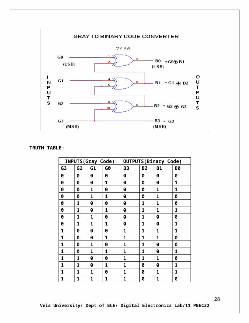
EXP. NO: 5 GRAY TO BINARY - CODE CONVERTER
DATE:
21Vels University/ Dept of ECE/ Digital Electronics Lab/11 PBEC32
AIM: To construct and verify the truth table of Gray to Binary code converter
APPARATUS REQUIRED:
PROCEDURE:
1. Give connections as per the circuit diagram2. Inputs are given to the circuit making high ‘1’ i.e. +5 V or + Vcc supply to the 14th pin
and for low ‘0’ i.e. GND to the 7th pin of gate IC3. Verify the truth table as given for the entire code converter
LOGIC DIAGRAM:
22Vels University/ Dept of ECE/ Digital Electronics Lab/11 PBEC32
S.NO Particular Name SPECIFICATION QUANTITY
123
Digital IC trainer kitIC 7486Connecting Wires
----QUADQUAD
131
TRUTH TABLE:
INPUTS(Gray Code) OUTPUTS(Binary Code)G3 G2 G1 G0 B3 B2 B1 B0
0 0 0 0 0 0 0 00 0 0 1 0 0 0 10 0 1 0 0 0 1 10 0 1 1 0 0 1 00 1 0 0 0 1 1 00 1 0 1 0 1 1 10 1 1 0 0 1 0 00 1 1 1 0 1 0 11 0 0 0 1 1 1 11 0 0 1 1 1 1 01 0 1 0 1 1 0 01 0 1 1 1 1 0 11 1 0 0 1 1 1 01 1 0 1 1 0 0 11 1 1 0 1 0 1 11 1 1 1 1 0 1 0
23Vels University/ Dept of ECE/ Digital Electronics Lab/11 PBEC32
RESULT: The code converter circuit was constructed and truth table is verified.
EXP. NO: 6 BCD TO EXCESS 3 - CODE CONVERTER
24Vels University/ Dept of ECE/ Digital Electronics Lab/11 PBEC32
DATE:AIM:
To construct and verify the truth table of BCD to Excess-3 code converter circuit.
APPARATUS REQUIRED:
S.NO Particular Name SPECIFICATION QUANTITY
1. Digital IC trainer kit 12. IC7486 QUAD 13. IC 7404 QUAD 14. IC 7408 QUAD 15. IC 7432 QUAD 16. Connecting Wires
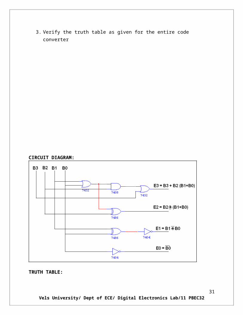
PROCEDURE:
1. Give connections as per the circuit diagram2. Inputs are given to the circuit making high ‘1’ i.e. +5 V or + Vcc supply to the 14th pin
and for low ‘0’ i.e. GND to the 7th pin of gate IC3. Verify the truth table as given for the entire code converter
CIRCUIT DIAGRAM:
25Vels University/ Dept of ECE/ Digital Electronics Lab/11 PBEC32
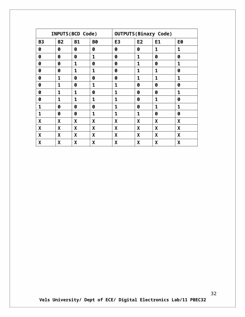
TRUTH TABLE:
INPUTS(BCD Code) OUTPUTS(Binary Code)
B3 B2 B1 B0 E3 E2 E1 E0
0 0 0 0 0 0 1 1
0 0 0 1 0 1 0 0
0 0 1 0 0 1 0 1
0 0 1 1 0 1 1 0
0 1 0 0 0 1 1 1
0 1 0 1 1 0 0 0
0 1 1 0 1 0 0 1
0 1 1 1 1 0 1 0
1 0 0 0 1 0 1 1
1 0 0 1 1 1 0 0
X X X X X X X X
X X X X X X X X
X X X X X X X X
X X X X X X X X
26Vels University/ Dept of ECE/ Digital Electronics Lab/11 PBEC32
RESULT:
The code converter circuit was constructed and truth table is verified
EXPT. NO. :7 DESIGN OF 4-BIT ADDER AND SUBTRACTORDATE:
27Vels University/ Dept of ECE/ Digital Electronics Lab/11 PBEC32
AIM: To design and implement 4-bit adder and subtractor using IC 7483.
APPARATUS REQUIRED:
Sl.No. COMPONENT SPECIFICATION QTY.
1. IC IC 7483 1
2. EX-OR GATE IC 7486 1
3. NOT GATE IC 7404 1
3. IC TRAINER KIT - 1
4. PATCH CORDS - 40
THEORY:
4 BIT BINARY ADDERS:
A binary adder is a digital circuit that produces the arithmetic sum of two binary
numbers. It can be constructed with full adders connected in cascade, with the output carry from
each full adder connected to the input carry of next full adder in chain.
The augends bits of ‘A’ and the addend bits of ‘B’ are designated by subscript numbers
from right to left, with subscript 0 denoting the least significant bits. The carries are connected in
chain through the full adder. The input carry to the adder is C0 and it ripples through the full
adder to the output carry C4.
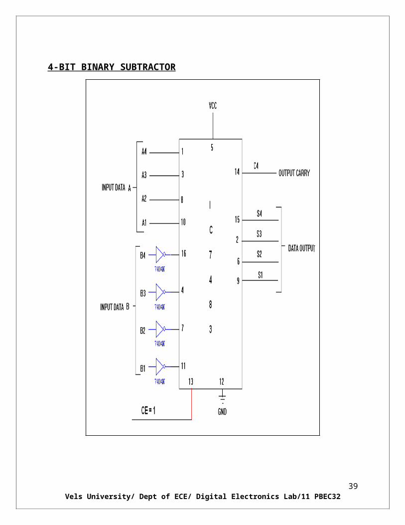
4 BIT BINARY SUBTRACTOR:
28Vels University/ Dept of ECE/ Digital Electronics Lab/11 PBEC32
The circuit for subtracting A-B consists of an adder with inverters, placed between each
data input ‘B’ and the corresponding input of full adder. The input carry C0 must be equal to 1
when performing subtraction.
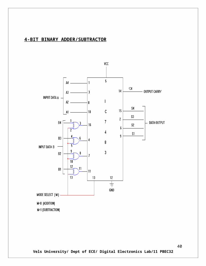
4 BIT BINARY ADDER/SUBTRACTOR:
The addition and subtraction operation can be combined into one circuit with one
common binary adder. The mode input M controls the operation. When M=0, the circuit is adder
circuit. When M=1, it becomes subtractor.
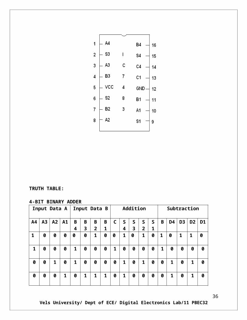
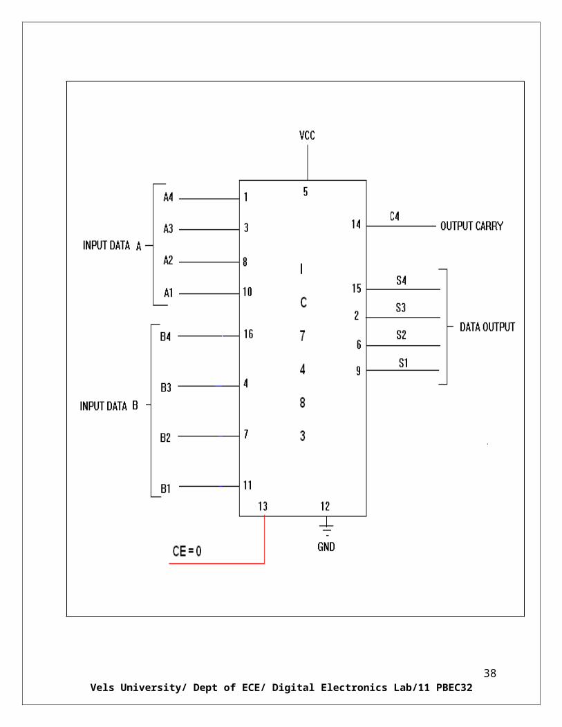
PIN DIAGRAM FOR IC 7483:
TRUTH TABLE:
4-BIT BINARY ADDER
29Vels University/ Dept of ECE/ Digital Electronics Lab/11 PBEC32
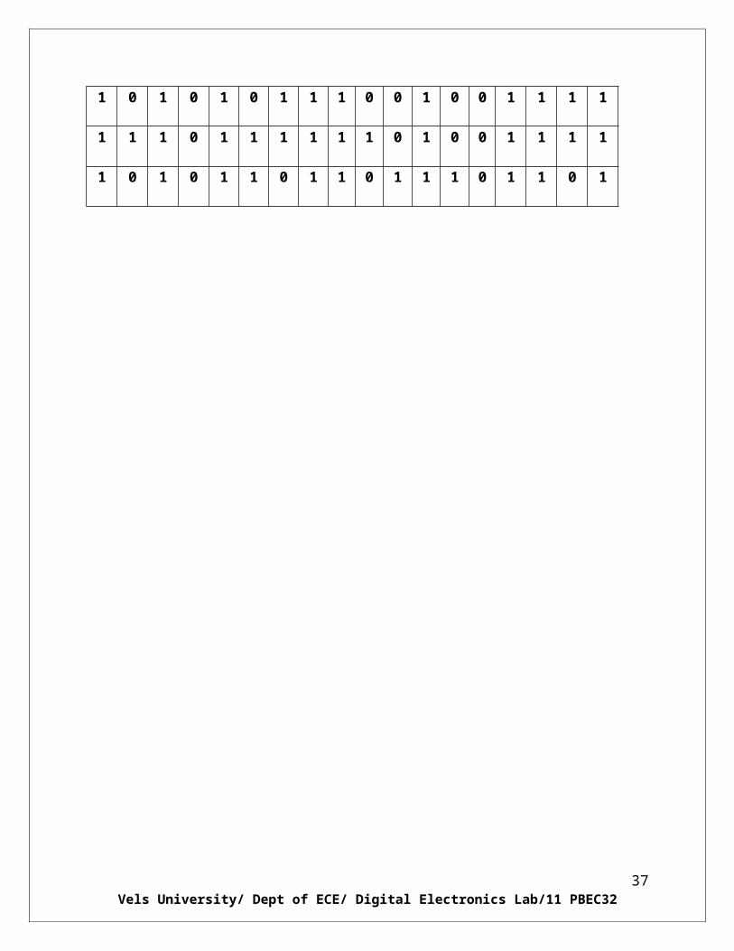
Input Data A Input Data B Addition Subtraction
A4 A3 A2 A1 B4 B3 B2 B1 C S4 S3 S2 S1 B D4 D3 D2 D1
1 0 0 0 0 0 1 0 0 1 0 1 0 1 0 1 1 0
1 0 0 0 1 0 0 0 1 0 0 0 0 1 0 0 0 0
0 0 1 0 1 0 0 0 0 1 0 1 0 0 1 0 1 0
0 0 0 1 0 1 1 1 0 1 0 0 0 0 1 0 1 0
1 0 1 0 1 0 1 1 1 0 0 1 0 0 1 1 1 1
1 1 1 0 1 1 1 1 1 1 0 1 0 0 1 1 1 1
1 0 1 0 1 1 0 1 1 0 1 1 1 0 1 1 0 1
30Vels University/ Dept of ECE/ Digital Electronics Lab/11 PBEC32
31Vels University/ Dept of ECE/ Digital Electronics Lab/11 PBEC32
4-BIT BINARY SUBTRACTOR
32Vels University/ Dept of ECE/ Digital Electronics Lab/11 PBEC32
4-BIT BINARY ADDER/SUBTRACTOR
33Vels University/ Dept of ECE/ Digital Electronics Lab/11 PBEC32
PROCEDURE:
(i) Connections were given as per circuit diagram.
(ii) Logical inputs were given as per truth table
(iii) Observe the logical output and verify with the truth tables.
RESULT:
The 4-bit adder and subtractor using IC 7483 were constructed and its truth table was verified.
34Vels University/ Dept of ECE/ Digital Electronics Lab/11 PBEC32
EXP. NO: 8
MULTIPLEXERDATE:
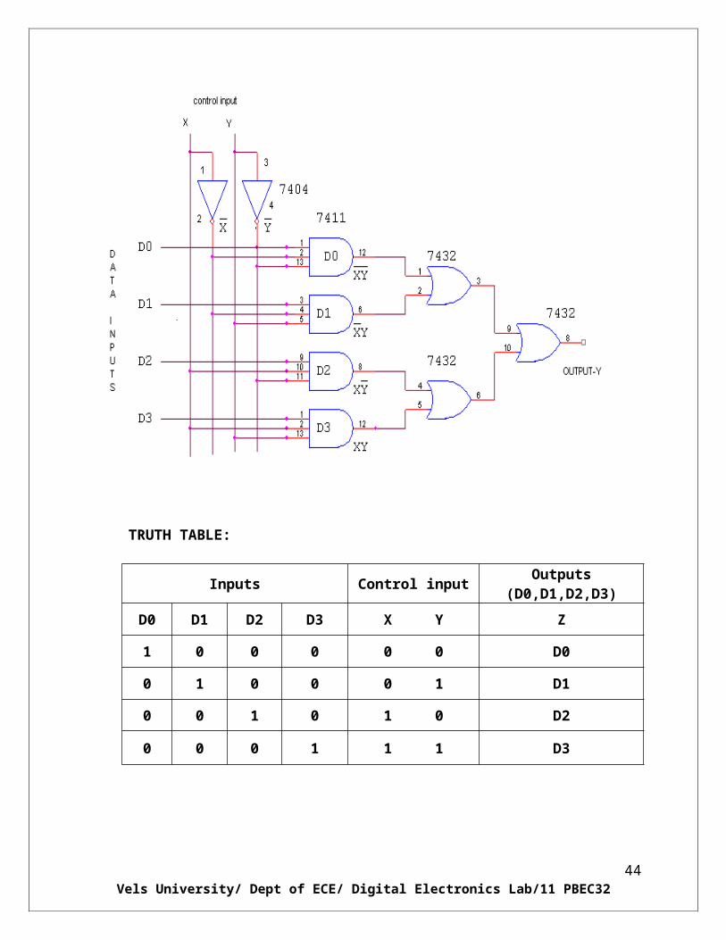
AIM: To construct and verify the truth table of multiplexer and circuits.
APPARATUS REQUIRED:
S.NO Particular Name SPECIFICATION QUANTITY
1
2
3
4
5
Digital IC trainer kit
IC7404
IC7432
IC7411
Connecting Wires
----
----
1
1
1
1
MULTIPLEXER
35Vels University/ Dept of ECE/ Digital Electronics Lab/11 PBEC32
CIRCUIT DIAGRAM:
TRUTH TABLE:
Inputs Control input Outputs (D0,D1,D2,D3)
D0 D1 D2 D3 X Y Z
1 0 0 0 0 0 D0
0 1 0 0 0 1 D1
0 0 1 0 1 0 D2
0 0 0 1 1 1 D3
36Vels University/ Dept of ECE/ Digital Electronics Lab/11 PBEC32
PROCEDURE:
1. Give connections as per the circuit diagram
2. Inputs are given to the circuit making high ‘1’, i.e. +5 V or + Vcc supply to the 16th pin
and for low ‘0’ i.e. GND to the 8th pin of the gate IC
3. Verify the truth table for the multiplexer as given
RESULT:
The Multiplexer circuit is constructed and truth table is verified.
EXP. NO: 9 DEMULTIPLEXER
37Vels University/ Dept of ECE/ Digital Electronics Lab/11 PBEC32
DATE:
AIM: To construct and verify the truth table of demultiplexer circuits
APPARATUS REQUIRED:
THEORY: DEMULTIPLEXER:
The function of Demultiplexer is in contrast to multiplexer function. It takes
information from one line and distributes it to a given number of output lines. For
this reason, the demultiplexer is also known as a data distributor. Decoder can also
be used as demultiplexer.
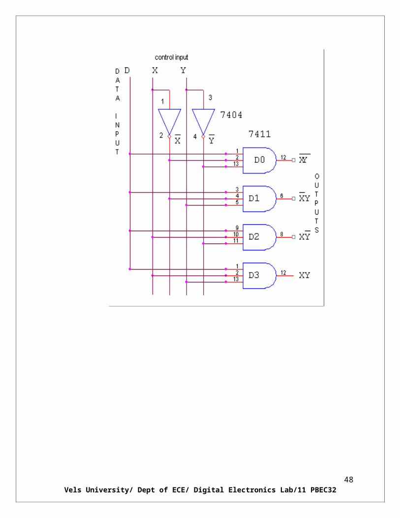
In the 1: 4 demultiplexer circuit, the data input line goes to all of the AND
gates. The data select lines enable only one gate at a time and the data on the data
input line will pass through the selected gate to the associated data output line.
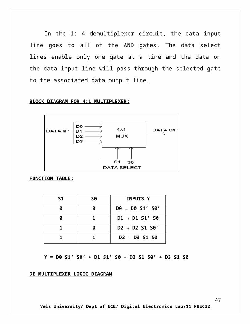
BLOCK DIAGRAM FOR 4:1 MULTIPLEXER:
FUNCTION TABLE:
38Vels University/ Dept of ECE/ Digital Electronics Lab/11 PBEC32
S.NO Particular Name SPECIFICATION QUANTITY
123
Digital IC trainer kitIC7404, IC7432 IC7411Connecting Wires
--------
1 1 each
2
S1 S0 INPUTS Y
0 0 D0 → D0 S1’ S0’
0 1 D1 → D1 S1’ S0
1 0 D2 → D2 S1 S0’
1 1 D3 → D3 S1 S0
Y = D0 S1’ S0’ + D1 S1’ S0 + D2 S1 S0’ + D3 S1 S0
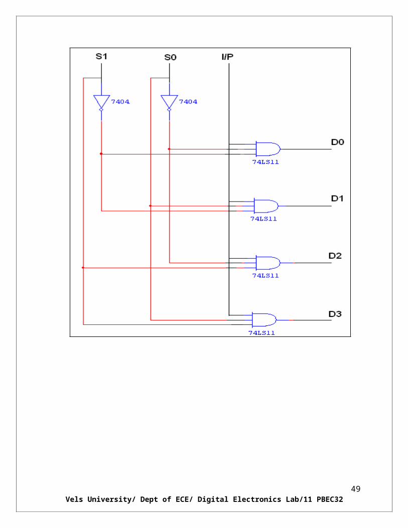
DE MULTIPLEXER LOGIC DIAGRAM
39Vels University/ Dept of ECE/ Digital Electronics Lab/11 PBEC32
40Vels University/ Dept of ECE/ Digital Electronics Lab/11 PBEC32
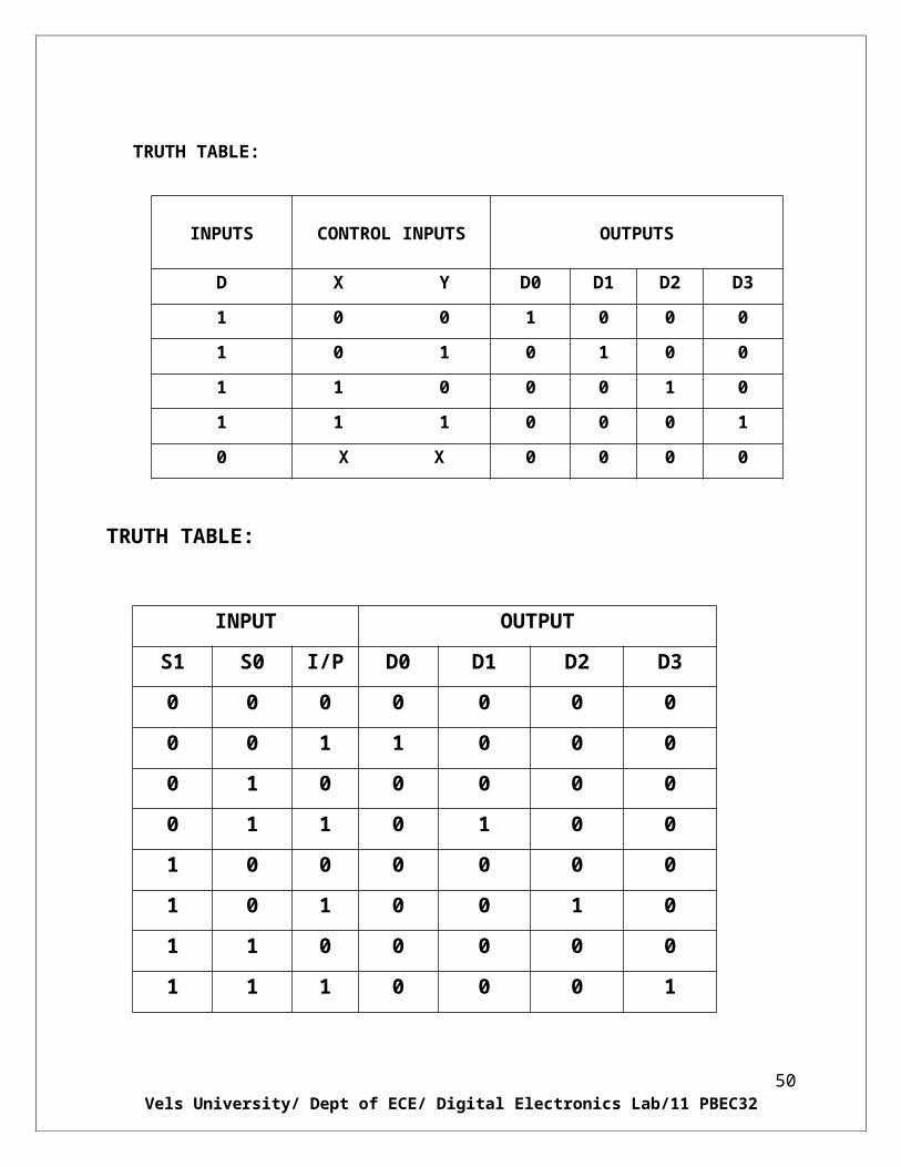
TRUTH TABLE:
INPUTS CONTROL INPUTS OUTPUTS
D X Y D0 D1 D2 D3
1 0 0 1 0 0 0
1 0 1 0 1 0 0
1 1 0 0 0 1 0
1 1 1 0 0 0 1
0 X X 0 0 0 0
TRUTH TABLE:
INPUT OUTPUT
S1 S0 I/P D0 D1 D2 D3
0 0 0 0 0 0 0
0 0 1 1 0 0 0
0 1 0 0 0 0 0
0 1 1 0 1 0 0
1 0 0 0 0 0 0
1 0 1 0 0 1 0
1 1 0 0 0 0 0
1 1 1 0 0 0 1
41Vels University/ Dept of ECE/ Digital Electronics Lab/11 PBEC32
PROCEDURE:
1. Give connections as per the circuit diagram
2. Inputs are given to the circuit making high ‘1’, i.e. +5 V or + Vcc supply to the
16th pin and for low ‘0’ i.e. GND to the 8th pin of the gate IC
3. Verify the truth table for the de multiplexer as given
RESULT:
The De Multiplexer circuit is constructed and truth table is verified.
42Vels University/ Dept of ECE/ Digital Electronics Lab/11 PBEC32
EXP. NO: 10 DESIGN AND IMPLEMENTATION OF MAGNITUDE COMPARATORDATE:
AIM: To design and implement
(i) 2 – bit magnitude comparator using basic gates.
(ii) 8 – bit magnitude comparator using IC 7485.
APPARATUS REQUIRED:
Sl.No. COMPONENT SPECIFICATION QTY.
1. AND GATE IC 7408 2
2. X-OR GATE IC 7486 1
3. OR GATE IC 7432 1
4. NOT GATE IC 7404 1
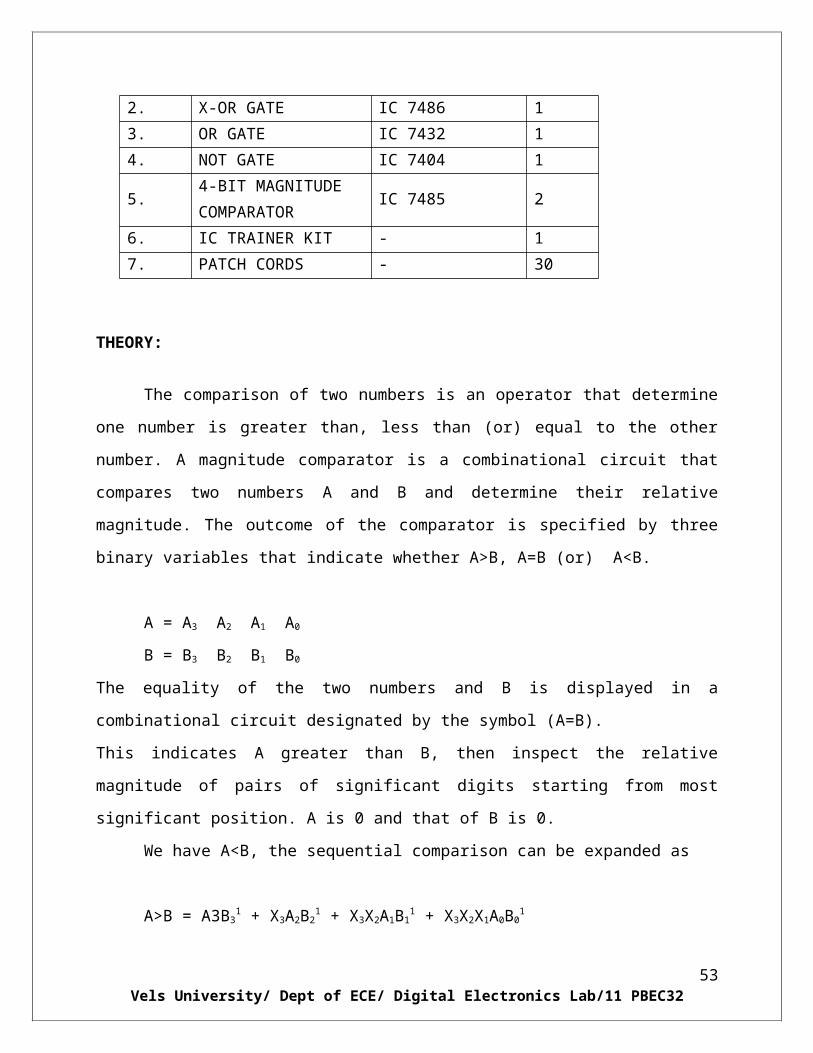
5.4-BIT MAGNITUDE COMPARATOR
IC 7485 2
6. IC TRAINER KIT - 1
7. PATCH CORDS - 30
THEORY:
The comparison of two numbers is an operator that determine one number is greater than,
less than (or) equal to the other number. A magnitude comparator is a combinational circuit that
compares two numbers A and B and determine their relative magnitude. The outcome of the
comparator is specified by three binary variables that indicate whether A>B, A=B (or) A<B.
A = A3 A2 A1 A0
B = B3 B2 B1 B0
43Vels University/ Dept of ECE/ Digital Electronics Lab/11 PBEC32
The equality of the two numbers and B is displayed in a combinational circuit designated by the
symbol (A=B).
This indicates A greater than B, then inspect the relative magnitude of pairs of significant digits
starting from most significant position. A is 0 and that of B is 0.
We have A<B, the sequential comparison can be expanded as
A>B = A3B31 + X3A2B2
1 + X3X2A1B11 + X3X2X1A0B0
1
A<B = A31B3 + X3A2
1B2 + X3X2A11B1 + X3X2X1A0
1B0
The same circuit can be used to compare the relative magnitude of two BCD digits.
Where, A = B is expanded as,
A = B = (A3 + B3) (A2 + B2) (A1 + B1) (A0 + B0)
x3 x2 x1 x0
44Vels University/ Dept of ECE/ Digital Electronics Lab/11 PBEC32
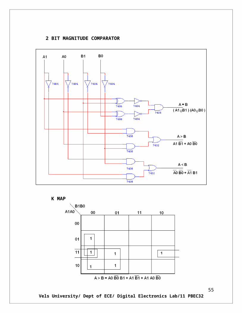
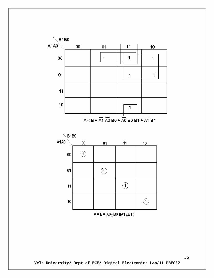
2 BIT MAGNITUDE COMPARATOR
K MAP
45Vels University/ Dept of ECE/ Digital Electronics Lab/11 PBEC32
46Vels University/ Dept of ECE/ Digital Electronics Lab/11 PBEC32
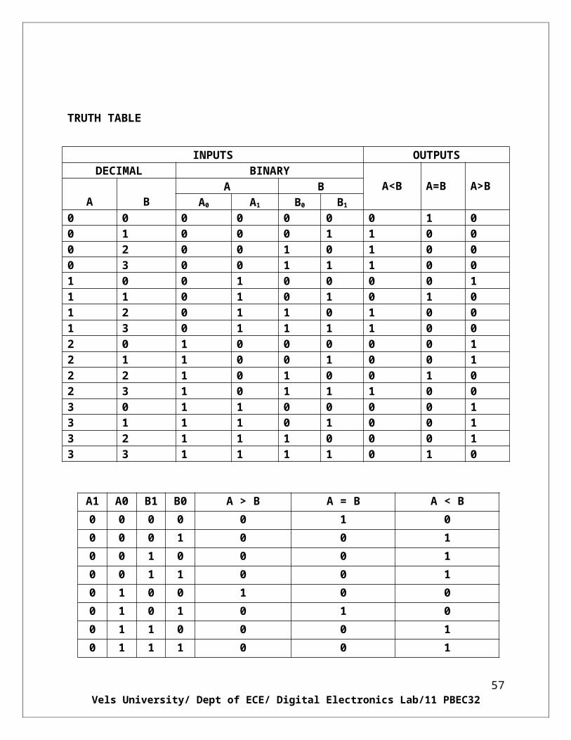
TRUTH TABLE
INPUTS OUTPUTSDECIMAL BINARY
A<B A=B A>BA B
A BA0 A1 B0 B1
0 0 0 0 0 0 0 1 00 1 0 0 0 1 1 0 00 2 0 0 1 0 1 0 00 3 0 0 1 1 1 0 01 0 0 1 0 0 0 0 11 1 0 1 0 1 0 1 01 2 0 1 1 0 1 0 01 3 0 1 1 1 1 0 02 0 1 0 0 0 0 0 12 1 1 0 0 1 0 0 12 2 1 0 1 0 0 1 02 3 1 0 1 1 1 0 03 0 1 1 0 0 0 0 1
47Vels University/ Dept of ECE/ Digital Electronics Lab/11 PBEC32
3 1 1 1 0 1 0 0 13 2 1 1 1 0 0 0 13 3 1 1 1 1 0 1 0
A1 A0 B1 B0 A > B A = B A < B
0 0 0 0 0 1 0
0 0 0 1 0 0 1
0 0 1 0 0 0 1
0 0 1 1 0 0 1
0 1 0 0 1 0 0
0 1 0 1 0 1 0
0 1 1 0 0 0 1
0 1 1 1 0 0 1
1 0 0 0 1 0 0
1 0 0 1 1 0 0
1 0 1 0 0 1 0
1 0 1 1 0 0 1
1 1 0 0 1 0 0
1 1 0 1 1 0 0
1 1 1 0 1 0 0
1 1 1 1 0 1 0
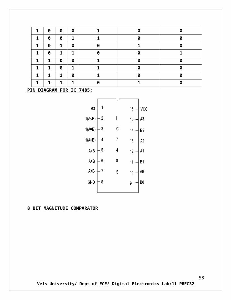
PIN DIAGRAM FOR IC 7485:
48Vels University/ Dept of ECE/ Digital Electronics Lab/11 PBEC32
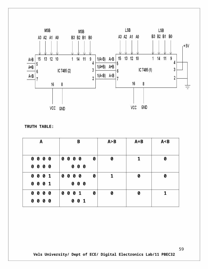
8 BIT MAGNITUDE COMPARATOR
TRUTH TABLE:
A B A>B A=B A<B
0 0 0 0 0 0 0 0 0 0 0 0 0 0 0 0 0 1 0
0 0 0 1 0 0 0 1 0 0 0 0 0 0 0 0 1 0 0
0 0 0 0 0 0 0 0 0 0 0 1 0 0 0 1 0 0 1
49Vels University/ Dept of ECE/ Digital Electronics Lab/11 PBEC32
PROCEDURE:
1. Give connections as per the circuit diagram
2. Inputs are given to the circuit making high ‘1’ i.e. +5 V or + Vcc supply to the 14 th pin
and for low ‘0’ i.e. GND to the 7th pin of the gate IC
3. Depending upon the values of A and B, the corresponding LED’s glow which indicates
the comparator Output
50Vels University/ Dept of ECE/ Digital Electronics Lab/11 PBEC32
RESULT:
Thus the comparator circuits were constructed and the truth table was verified.
EXP. NO: 11 ENCODER
DATE:
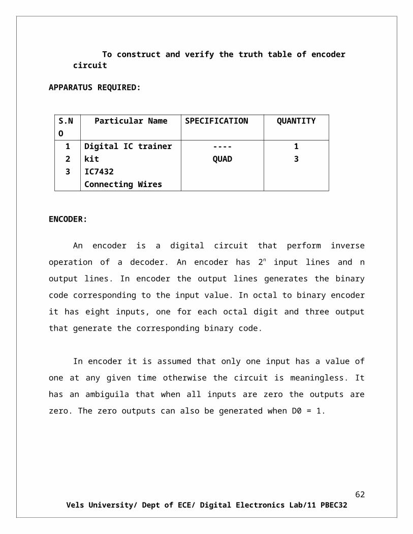
AIM : To construct and verify the truth table of encoder circuit
APPARATUS REQUIRED:
S.NO Particular Name SPECIFICATION QUANTITY123
Digital IC trainer kitIC7432 Connecting Wires
----QUAD
13
ENCODER:
51Vels University/ Dept of ECE/ Digital Electronics Lab/11 PBEC32
An encoder is a digital circuit that perform inverse operation of a decoder. An encoder
has 2n input lines and n output lines. In encoder the output lines generates the binary code
corresponding to the input value. In octal to binary encoder it has eight inputs, one for each octal
digit and three output that generate the corresponding binary code.
In encoder it is assumed that only one input has a value of one at any given time
otherwise the circuit is meaningless. It has an ambiguila that when all inputs are zero the outputs
are zero. The zero outputs can also be generated when D0 = 1.
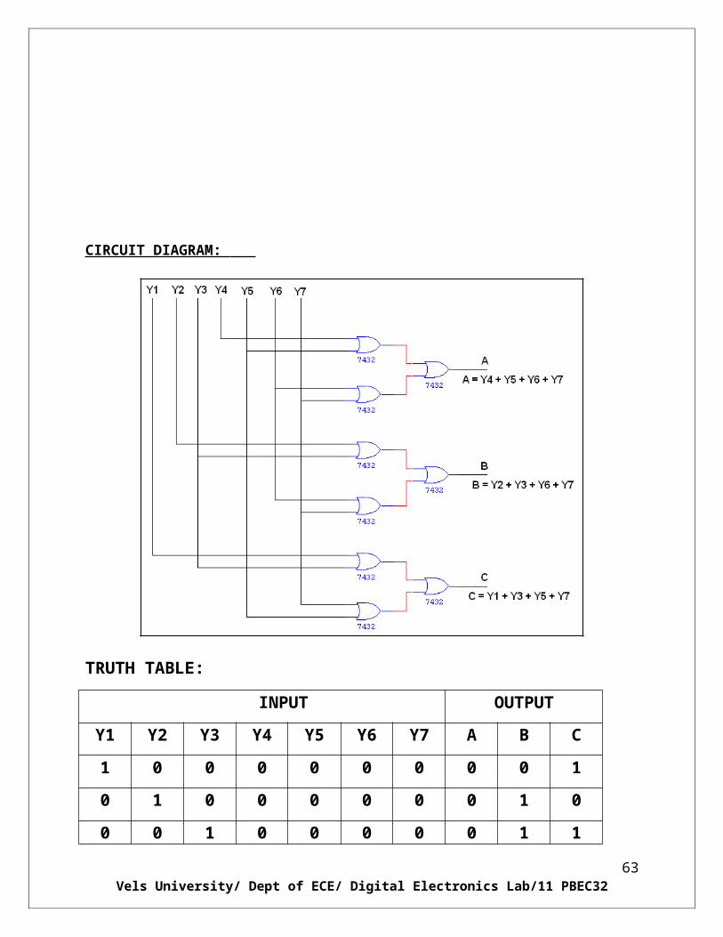
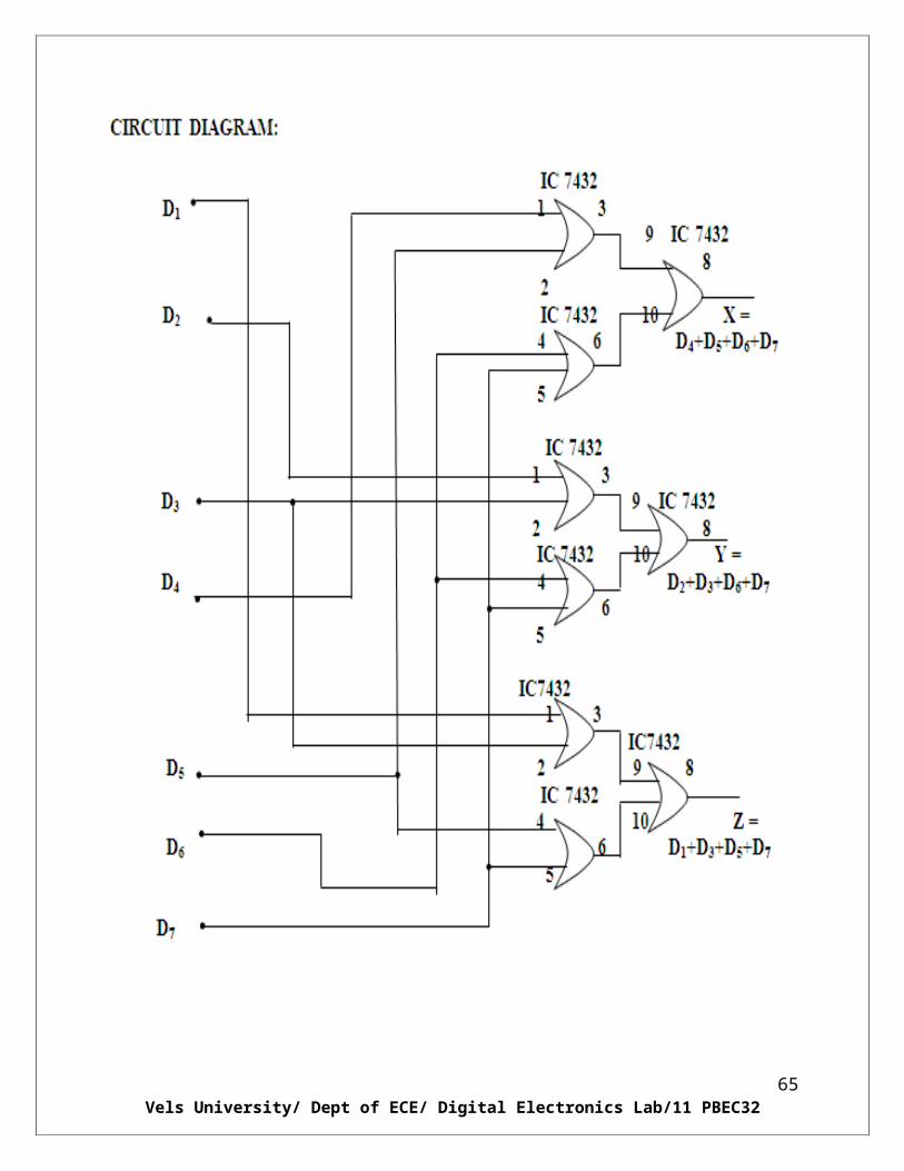
CIRCUIT DIAGRAM:
52Vels University/ Dept of ECE/ Digital Electronics Lab/11 PBEC32
TRUTH TABLE:
INPUT OUTPUT
Y1 Y2 Y3 Y4 Y5 Y6 Y7 A B C
1 0 0 0 0 0 0 0 0 1
0 1 0 0 0 0 0 0 1 0
0 0 1 0 0 0 0 0 1 1
0 0 0 1 0 0 0 1 0 0
0 0 0 0 1 0 0 1 0 1
0 0 0 0 0 1 0 1 1 0
0 0 0 0 0 0 1 1 1 1
53Vels University/ Dept of ECE/ Digital Electronics Lab/11 PBEC32
54Vels University/ Dept of ECE/ Digital Electronics Lab/11 PBEC32
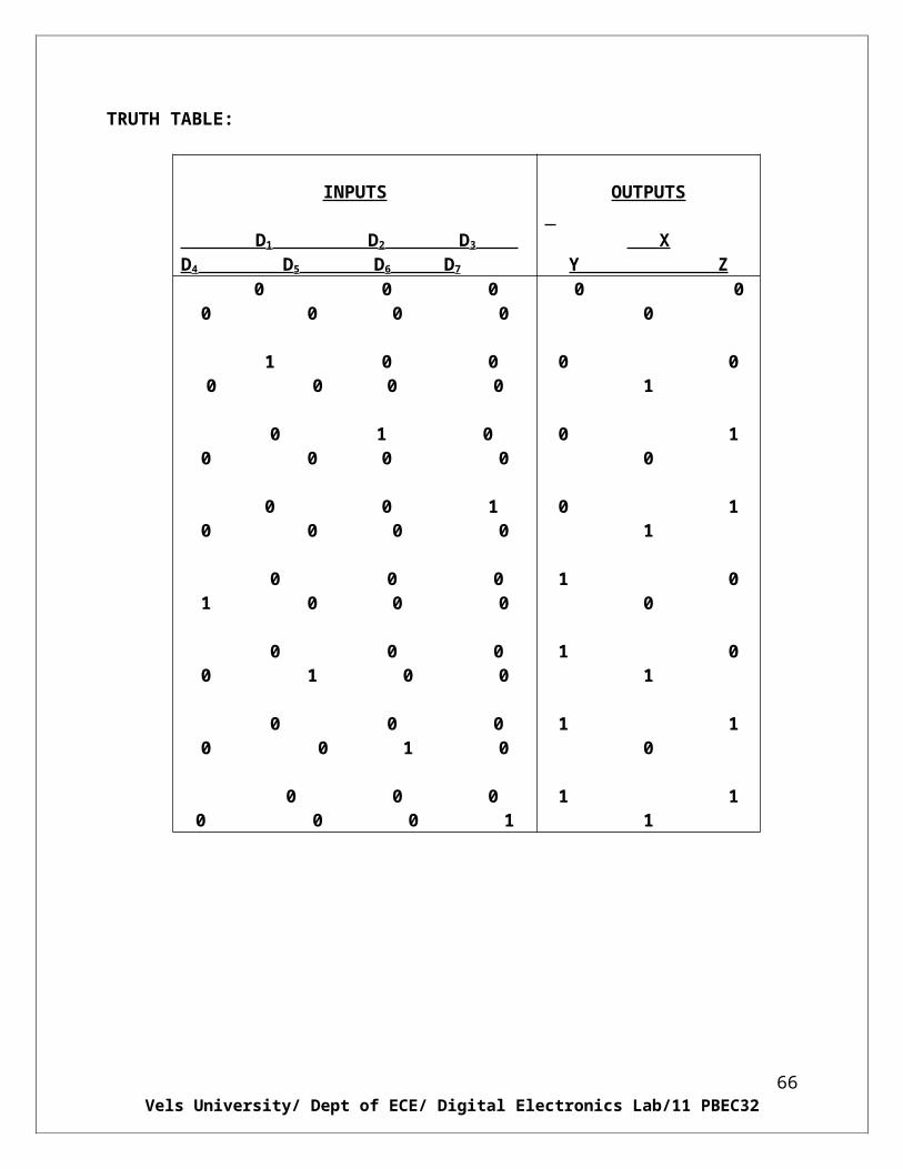
TRUTH TABLE:
INPUTS
D1 D2 D3 D4 D5 D6 D7
OUTPUTS
X Y Z 0 0 0 0 0 0 0
1 0 0 0 0 0 0
0 1 0 0 0 0 0
0 0 1 0 0 0 0
0 0 0 1 0 0 0
0 0 0 0 1 0 0
0 0 0 0 0 1 0
0 0 0 0 0 0 1
0 0 0
0 0 1
0 1 0
0 1 1
1 0 0
1 0 1
1 1 0
1 1 1
55Vels University/ Dept of ECE/ Digital Electronics Lab/11 PBEC32
PROCEDURE :
1. Give connections as per the circuit diagram2. Inputs are given to the circuit making high ‘1’ i.e. +5 V or + Vcc supply to the 14th pin
and for low ‘0’ i.e. GND to the 7th
3. pin of the gate IC
4. Verify the truth table as given for the encoder
RESULT:
The Encoder circuit is constructed and truth table is verified.
56Vels University/ Dept of ECE/ Digital Electronics Lab/11 PBEC32
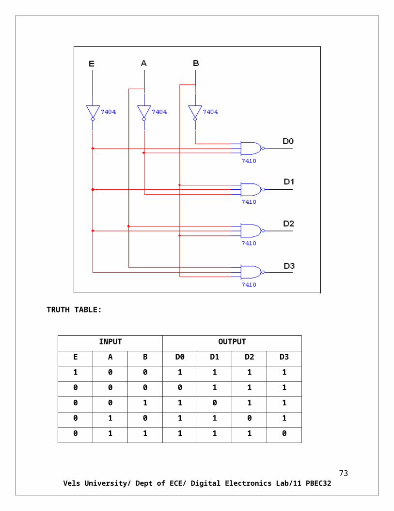
EXP. NO: 12 DECODER
DATE:
AIM: To construct and verify the truth table of decoder circuit
APPARATUS REQUIRED:
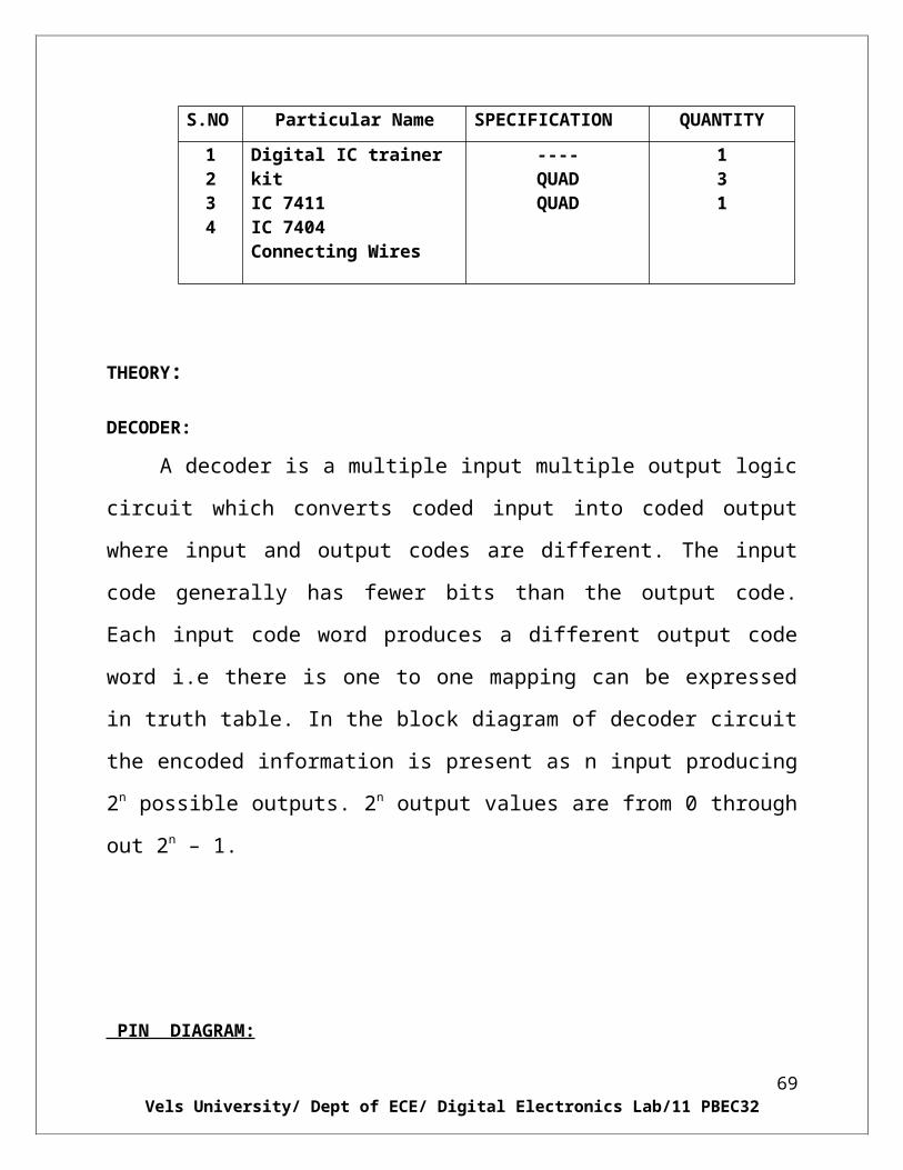
S.NO Particular Name SPECIFICATION QUANTITY
1234
Digital IC trainer kitIC 7411IC 7404 Connecting Wires
----QUADQUAD
131
THEORY:
DECODER:
A decoder is a multiple input multiple output logic circuit which converts
coded input into coded output where input and output codes are different. The
input code generally has fewer bits than the output code. Each input code word
produces a different output code word i.e there is one to one mapping can be
expressed in truth table. In the block diagram of decoder circuit the encoded
information is present as n input producing 2n possible outputs. 2n output values are
from 0 through out 2n – 1.
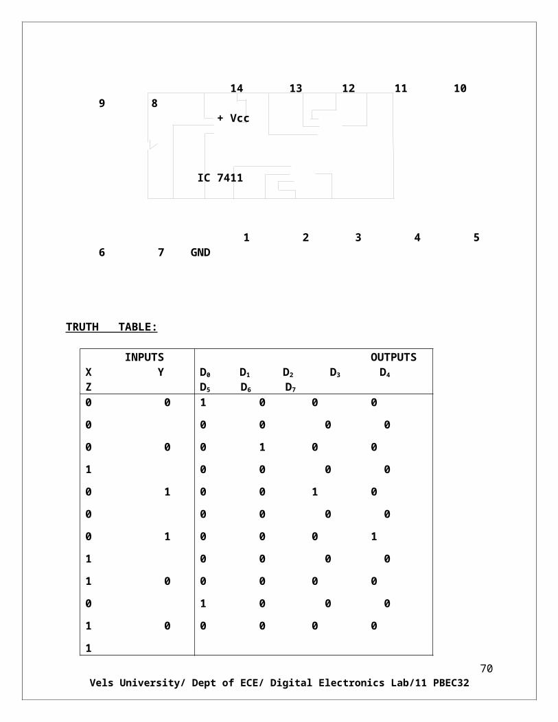
PIN DIAGRAM:
57Vels University/ Dept of ECE/ Digital Electronics Lab/11 PBEC32
14 13 12 11 10 9 8 + Vcc
IC 7411 1 2 3 4 5 6 7 GND
TRUTH TABLE:
INPUTSX Y Z
OUTPUTSD0 D1 D2 D3 D4 D5 D6 D7
0 0 0
0 0 1
0 1 0
0 1 1
1 0 0
1 0 1
1 1 0
1 1 1
1 0 0 0 0 0 0 0
0 1 0 0 0 0 0 0
0 0 1 0 0 0 0 0
0 0 0 1 0 0 0 0
0 0 0 0 1 0 0 0
0 0 0 0 0 1 0 0
0 0 0 0 0 0 1 0
0 0 0 0 0 0 0 1
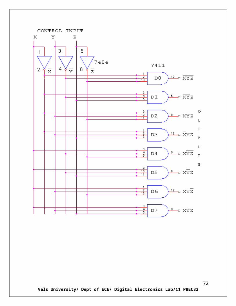
CIRCUIT DIAGRAM:
58Vels University/ Dept of ECE/ Digital Electronics Lab/11 PBEC32
59Vels University/ Dept of ECE/ Digital Electronics Lab/11 PBEC32
TRUTH TABLE:
INPUT OUTPUT
E A B D0 D1 D2 D3
1 0 0 1 1 1 1
0 0 0 0 1 1 1
0 0 1 1 0 1 1
0 1 0 1 1 0 1
0 1 1 1 1 1 0
60Vels University/ Dept of ECE/ Digital Electronics Lab/11 PBEC32
PROCEDURE:
1. Give connections as per the circuit diagram
2. Inputs are given to the circuit making high ‘1’ i.e. +5 V or + Vcc supply to
the 14th pin and for low ‘0’ i.e. GND to the 7th pin of the gate IC
3. Verify the truth table as given for the decoder circuit
RESULT:
The decoder circuit is constructed and truth table is verified.
EXP. NO:13 16 BIT ODD/EVEN PARITY CHECKER/GENERATOR
61Vels University/ Dept of ECE/ Digital Electronics Lab/11 PBEC32
DATE:
AIM:
To design and implement 16 bit odd/even parity checker generator using IC
74180.
APPARATUS REQUIRED:
Sl. No. COMPONENT SPECIFICATION QTY.
1. NOT GATE IC 7404 1
1. IC 74180 2
2. IC TRAINER KIT - 1
3. PATCH CORDS - 30
THEORY:
A parity bit is used for detecting errors during transmission of binary
information. A parity bit is an extra bit included with a binary message to make the
number is either even or odd. The message including the parity bit is transmitted
and then checked at the receiver ends for errors.
An error is detected if the checked parity bit doesn’t correspond to the one
transmitted. The circuit that generates the parity bit in the transmitter is called a
‘parity generator’ and the circuit that checks the parity in the receiver is called a
‘parity checker’.
In even parity, the added parity bit will make the total number is even
amount. In odd parity, the added parity bit will make the total number is odd
amount. The parity checker circuit checks for possible errors in the transmission.
If the information is passed in even parity, then the bits required must have
an even number of 1’s. An error occur during transmission, if the received bits
62Vels University/ Dept of ECE/ Digital Electronics Lab/11 PBEC32
have an odd number of 1’s indicating that one bit has changed in value during
transmission.
PIN DIAGRAM FOR IC 74180:
FUNCTION TABLE:
INPUTS OUTPUTS
Number of High DataInputs (I0 – I7)
PE PO ∑E ∑O
EVEN 1 0 1 0ODD 1 0 0 1
EVEN 0 1 0 1ODD 0 1 1 0
X 1 1 0 0X 0 0 1 1
63Vels University/ Dept of ECE/ Digital Electronics Lab/11 PBEC32
LOGIC DIAGRAM:
16 BIT ODD/EVEN PARITY CHECKER
TRUTH TABLE:
I7 I6 I5 I4 I3 I2 I1 I0 I7’I6’I5’I4’I3’I2’11’ I0’ Active ∑E ∑O
0 0 0 0 0 0 0 1 0 0 0 0 0 0 0 0 1 1 0
0 0 0 0 0 1 1 0 0 0 0 0 0 1 1 0 0 1 0
0 0 0 0 0 1 1 0 0 0 0 0 0 1 1 0 1 0 1
64Vels University/ Dept of ECE/ Digital Electronics Lab/11 PBEC32
16 BIT ODD/EVEN PARITY GENERATORS
TRUTH TABLE:
I7 I6 I5 I4 I3 I2 I1 I0 I7 I6 I5 I4 I3 I2 I1 I0 Active ∑E ∑O
1 1 0 0 0 0 0 0 1 1 0 0 0 0 0 0 1 1 0
1 1 0 0 0 0 0 0 1 1 0 0 0 0 0 0 0 0 1
1 1 0 0 0 0 0 0 0 1 0 0 0 0 0 0 0 1 0
65Vels University/ Dept of ECE/ Digital Electronics Lab/11 PBEC32
PROCEDURE:
(i) Connections are given as per circuit diagram.
(ii) Logical inputs are given as per circuit diagram.
(iii) Observe the output and verify the truth table.
RESULT:
The 16 bit odd/even parity checker generator using IC 74180 was constructed and
its truth table was verified
EXP. NO:14 DESIGN AND IMPLEMENTATION OF SHIFT
66Vels University/ Dept of ECE/ Digital Electronics Lab/11 PBEC32
REGISTERDATE:
AIM:
To design and implement
(i) Serial in serial out (ii) Serial in parallel out (iii) Parallel in serial out (iv) Parallel in parallel out
APPARATUS REQUIRED:
Sl.No. COMPONENT SPECIFICATION QTY.
1. D FLIP FLOP IC 7474 2
2. OR GATE IC 7432 1
3. IC TRAINER KIT - 1
4. PATCH CORDS - 35
THEORY:
A register is capable of shifting its binary information in one or both directions is known
as shift register. The logical configuration of shift register consist of a D-Flip flop cascaded with
output of one flip flop connected to input of next flip flop. All flip flops receive common clock
pulses which causes the shift in the output of the flip flop. The simplest possible shift register is
one that uses only flip flop. The output of a given flip flop is connected to the input of next flip
flop of the register. Each clock pulse shifts the content of register one bit position to right.
67Vels University/ Dept of ECE/ Digital Electronics Lab/11 PBEC32
PIN DIAGRAM:
LOGIC DIAGRAM:
SERIAL IN SERIAL OUT:
68Vels University/ Dept of ECE/ Digital Electronics Lab/11 PBEC32
TRUTH TABLE:
CLK Serial in Serial out
1 1 0
2 0 0
3 0 0
4 1 1
5 X 0
6 X 0
7 X 1
LOGIC DIAGRAM:
SERIAL IN PARALLEL OUT:
TRUTH TABLE:
CLK DATA
OUTPUT
QA QB QC QD
1 1 1 0 0 0
2 0 0 1 0 0
3 0 0 0 1 1
4 1 1 0 0 1
69Vels University/ Dept of ECE/ Digital Electronics Lab/11 PBEC32
LOGIC DIAGRAM:
PARALLEL IN SERIAL OUT:
TRUTH TABLE:
CLK Q3 Q2 Q1 Q0 O/P
0 1 0 0 1 1
1 0 0 0 0 0
2 0 0 0 0 0
3 0 0 0 0 1
70Vels University/ Dept of ECE/ Digital Electronics Lab/11 PBEC32
LOGIC DIAGRAM:
PARALLEL IN PARALLEL OUT:
TRUTH TABLE:
CLK
DATA INPUT OUTPUT
DA DB DC DD QA QB QC QD
1 1 0 0 1 1 0 0 1
2 1 0 1 0 1 0 1 0
71Vels University/ Dept of ECE/ Digital Electronics Lab/11 PBEC32
PROCEDURE:
(i) Connections are given as per circuit diagram.
(ii) Logical inputs are given as per circuit diagram.
(iii) Observe the output and verify the truth table.
RESULT: The shift register circuits were constructed and its truth table was verified.
72Vels University/ Dept of ECE/ Digital Electronics Lab/11 PBEC32
EXP. NO: 153 BIT ODD/EVEN PARITY GENERATOR
DATE:
AIM: To construct and verify the truth table of parity generator circuits
APPARATUS REQUIRED:
S.NO Particular Name SPECIFICATION QUANTITY123
Digital IC trainer kit IC 7486, IC 7404 Connecting Wires
----QUAD
11 each
PROCEDURE:
1. Give connections as per the circuit diagram
2. Inputs are given to the circuit making high ‘1’ i.e. +5 V or + Vcc supply to the 14 th pin
and for low ‘0’ i.e. GND to the 7th pin of the gate IC
3. Depending upon the truth table, if the LED glow it represents ‘1’ and else it represents
‘0’
4. Verify the truth table as given
73Vels University/ Dept of ECE/ Digital Electronics Lab/11 PBEC32
TRUTH TABLE
3- bit MessageX Y Z
Parity bit Generated (P)
0 0 00 0 10 1 00 1 11 0 01 0 11 1 01 1 1
10010110
74Vels University/ Dept of ECE/ Digital Electronics Lab/11 PBEC32
RESULT:
The 3 – bit even parity generator circuit is constructed and its truth table was verified.
75Vels University/ Dept of ECE/ Digital Electronics Lab/11 PBEC32


![anthony.sogang.ac.kranthony.sogang.ac.kr/KoreaReview/KoreaReviewVolume6-04.docx · Web viewTHE KOREA REVIEW . APRIL, 1906. [121] Are the Koreans Increasing in Numbers? It will be](https://img.pdfslide.us/doc/110x75/5d57465288c9931c088b99f7/-web-viewthe-korea-review-april-1906-121-are-the-koreans-increasing-in.jpg)