Embed Size (px)
Citation preview
Organic Electronics, Spring 2006, Dr. D. Knipp
1Organic Circuits
Information:http://www.faculty.iu-bremen.de/course/c300331a/
����������
Ref.: Apple
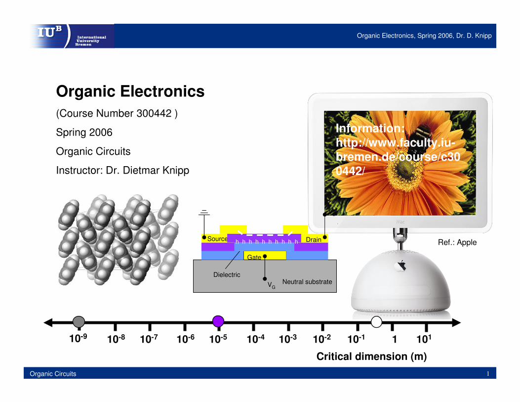
Information:http://www.faculty.iu-bremen.de/course/c300442/
Dielectric
e e e e e e e e
Gate
VGNeutral substrate
Source Drain
VD
h h h h h h h h h h
101110-110-210-310-410-510-610-8
Critical dimension (m)
10-710-9
Organic Electronics(Course Number 300442 )
Spring 2006
Organic Circuits
Instructor: Dr. Dietmar Knipp
Organic Electronics, Spring 2006, Dr. D. Knipp
2Organic Circuits
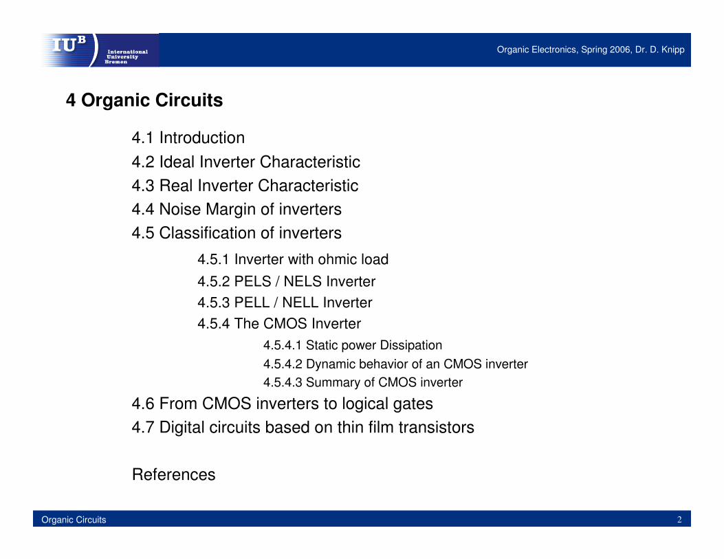
4 Organic Circuits
4.1 Introduction4.2 Ideal Inverter Characteristic4.3 Real Inverter Characteristic4.4 Noise Margin of inverters4.5 Classification of inverters
4.5.1 Inverter with ohmic load4.5.2 PELS / NELS Inverter4.5.3 PELL / NELL Inverter4.5.4 The CMOS Inverter
4.5.4.1 Static power Dissipation4.5.4.2 Dynamic behavior of an CMOS inverter4.5.4.3 Summary of CMOS inverter
4.6 From CMOS inverters to logical gates4.7 Digital circuits based on thin film transistors
References

Organic Electronics, Spring 2006, Dr. D. Knipp
3Organic Circuits
4.1 Introduction
In the following we will discuss the realization of CMOS circuits and its advantages. We will discuss the implementation of a CMOS inverter which is the bases of all digital gates. All other logical gates like OR, AND, NOR, and NAND can be derived from an inverter structure.
Layout of a CMOS inverter. Photo of a PELS inverter.
Ref.: Hodges & Jackson, Analysis and Design of Digital Circuits Ref.: G. Schmid, Infineon Technologies

Organic Electronics, Spring 2006, Dr. D. Knipp
4Organic Circuits
4.2 Ideal Inverter Characteristic
Different types of inverters can be distinguished depending on the circuit implementation. In the ideal case the static characteristic of an inverter (Voltage transfer curve, VTC) is described by a sharp transition from one state to second state.
Voltage transfer characteristic of an ideal inverter.
Input range Output range
Ref.: Hodges & Jackson, Analysis and Design of Digital Circuits

Organic Electronics, Spring 2006, Dr. D. Knipp
5Organic Circuits
4.3 Real Inverter Characteristic
However, ideal inverters can not be realized.
Voltage transfer characteristic of a real inverter.
Input range Output range
Ref.: Hodges & Jackson, Analysis and Design of Digital Circuits
Organic Electronics, Spring 2006, Dr. D. Knipp
6Organic Circuits
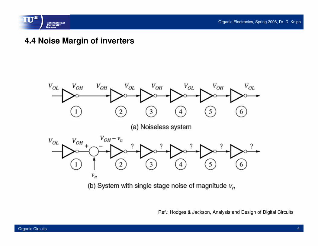
4.4 Noise Margin of inverters
Ref.: Hodges & Jackson, Analysis and Design of Digital Circuits
Organic Electronics, Spring 2006, Dr. D. Knipp
7Organic Circuits
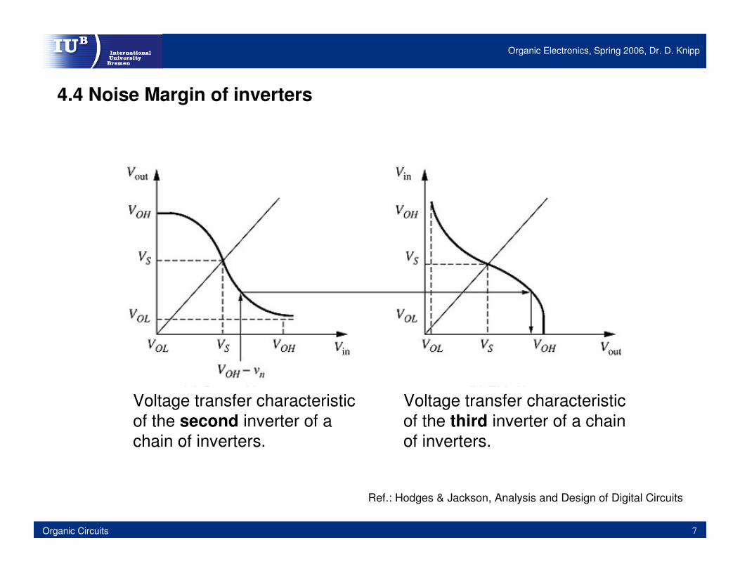
4.4 Noise Margin of inverters
Voltage transfer characteristic of the second inverter of a chain of inverters.
Voltage transfer characteristic of the third inverter of a chain of inverters.
Ref.: Hodges & Jackson, Analysis and Design of Digital Circuits

Organic Electronics, Spring 2006, Dr. D. Knipp
8Organic Circuits
4.4 Noise Margin of inverters
Ref.: Hodges & Jackson, Analysis and Design of Digital Circuits
The input and output signal of an inverter have to be within the noise margin of an inverter. Otherwise the input or output signal of an inverter is undefined.
Organic Electronics, Spring 2006, Dr. D. Knipp
9Organic Circuits
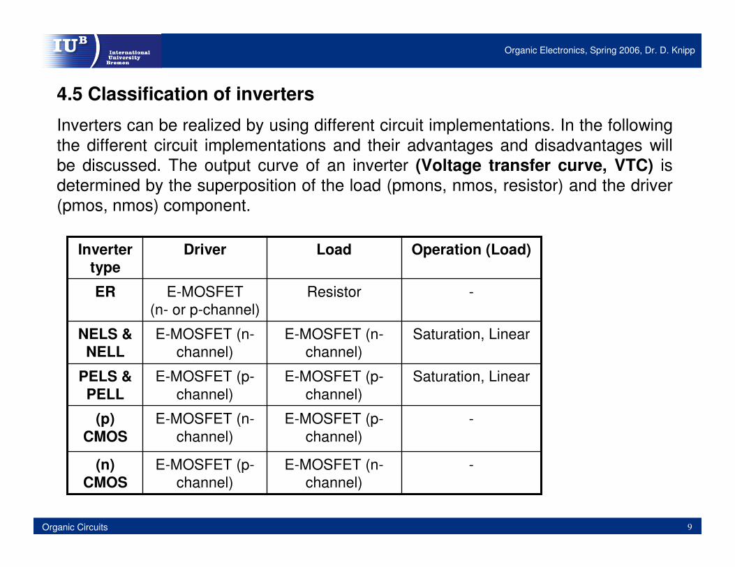
-E-MOSFET (n-channel)
E-MOSFET (p-channel)
(n) CMOS
-E-MOSFET (p-channel)
E-MOSFET (n-channel)
(p) CMOS
Saturation, LinearE-MOSFET (p-channel)
E-MOSFET (p-channel)
PELS & PELL
Saturation, LinearE-MOSFET (n-channel)
E-MOSFET (n-channel)
NELS &NELL
-ResistorE-MOSFET(n- or p-channel)
ER
Operation (Load)LoadDriverInverter type
4.5 Classification of inverters
Inverters can be realized by using different circuit implementations. In the following the different circuit implementations and their advantages and disadvantages will be discussed. The output curve of an inverter (Voltage transfer curve, VTC) is determined by the superposition of the load (pmons, nmos, resistor) and the driver (pmos, nmos) component.
Organic Electronics, Spring 2006, Dr. D. Knipp
10Organic Circuits
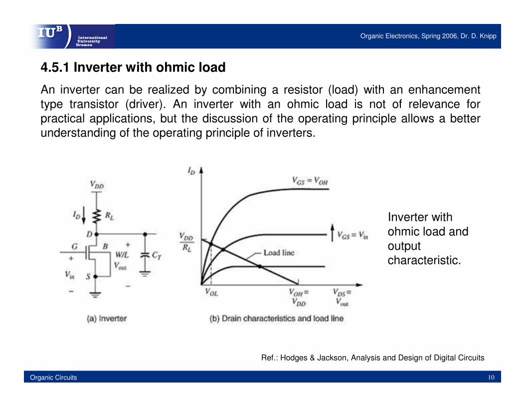
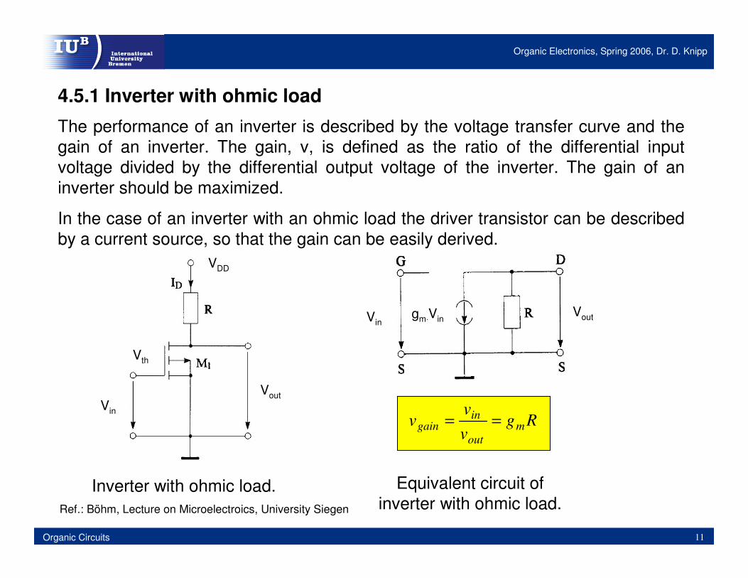
4.5.1 Inverter with ohmic load
An inverter can be realized by combining a resistor (load) with an enhancement type transistor (driver). An inverter with an ohmic load is not of relevance for practical applications, but the discussion of the operating principle allows a better understanding of the operating principle of inverters.
Ref.: Hodges & Jackson, Analysis and Design of Digital Circuits
Inverter with ohmic load and output characteristic.
Organic Electronics, Spring 2006, Dr. D. Knipp
11Organic Circuits
Vin
Vout
Vth
VDD
Inverter with ohmic load. Equivalent circuit of inverter with ohmic load.
VinVoutgm⋅Vin
Rgvv
v mout
ingain ==
4.5.1 Inverter with ohmic load
The performance of an inverter is described by the voltage transfer curve and the gain of an inverter. The gain, v, is defined as the ratio of the differential input voltage divided by the differential output voltage of the inverter. The gain of an inverter should be maximized.
In the case of an inverter with an ohmic load the driver transistor can be described by a current source, so that the gain can be easily derived.
Ref.: Böhm, Lecture on Microelectroics, University Siegen
Organic Electronics, Spring 2006, Dr. D. Knipp
12Organic Circuits
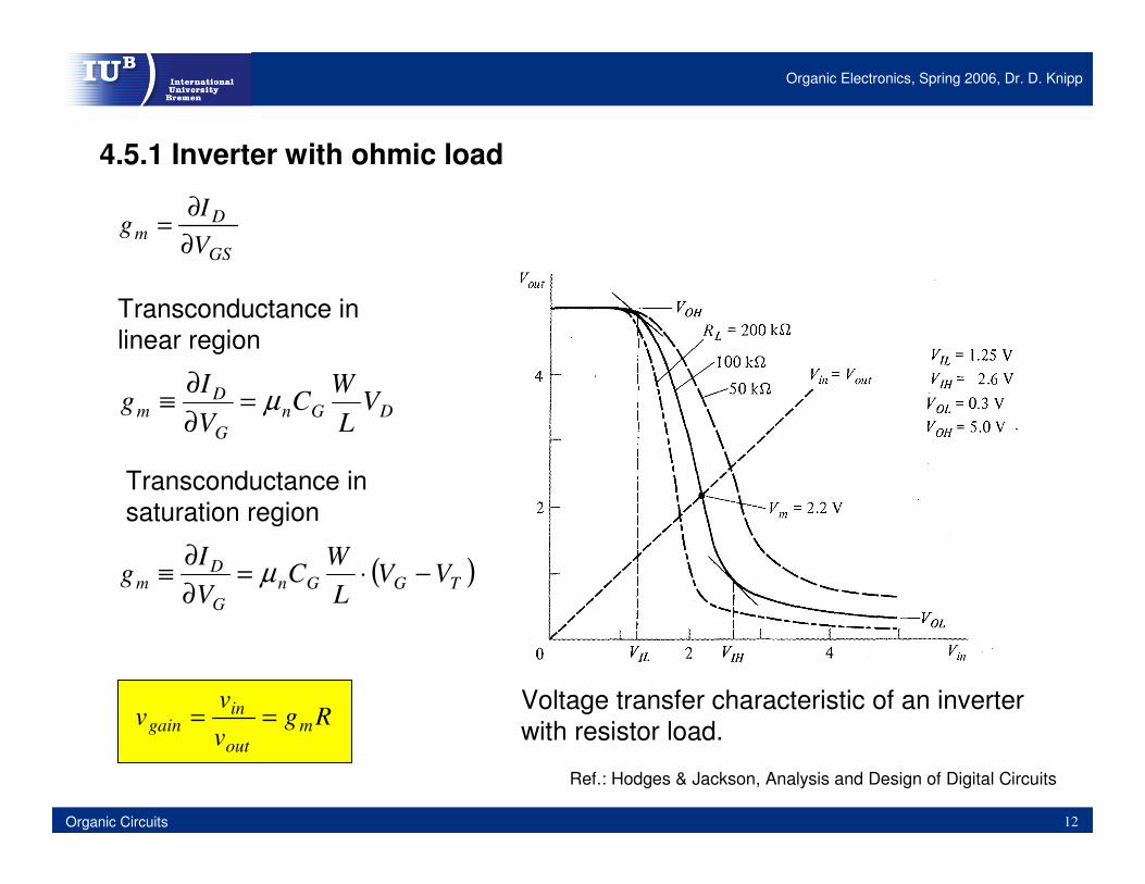
GS
Dm V
Ig
∂∂
=
DGnG
Dm V
LW
CVI
g µ=∂∂≡
( )TGGnG
Dm VV
LW
CVI
g −⋅=∂∂≡ µ
Transconductance in linear region
Transconductance in saturation region
4.5.1 Inverter with ohmic load
Voltage transfer characteristic of an inverter with resistor load.
Ref.: Hodges & Jackson, Analysis and Design of Digital Circuits
Rgvv
v mout
ingain ==

Organic Electronics, Spring 2006, Dr. D. Knipp
13Organic Circuits
4.5.1 Inverter with ohmic load
The gain of an inverter with ohmic load can be increased by increasing the load resistance and the W/L ratio of the transistor (driver). The W/L ratio can be increased by choosing a short but wide channel.
However, the gain is not the only parameter, which has to be optimized when developing an inverter. In addition to the gain (static behavior) the dynamic behavior has to be taken into account. If we assume that the inverter drives another logic gate like an inverter, and the inverter exhibits an input capacitance it is obvious to see that an increase of the load resistance will increase the time constant (switching speed) of the inverter. A similar behavior is observed if the width of the transistor is increased. The increased width leads to a improved gain, but the input capacitance of the inverter is increased as well, so that the switching speed of the inverter is reduced.
An inverter with an ohmic load has an additional disadvantage. It is difficult to realized resistors by using classical semiconductor processes.
Therefore, the resistor is usually replaced by a transistor which operates as a load.
Organic Electronics, Spring 2006, Dr. D. Knipp
14Organic Circuits
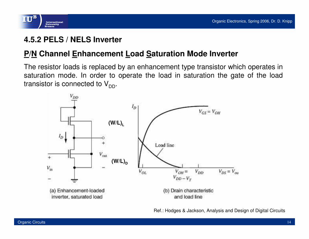
4.5.2 PELS / NELS Inverter
P/N Channel Enhancement Load Saturation Mode Inverter
The resistor loads is replaced by an enhancement type transistor which operates in saturation mode. In order to operate the load in saturation the gate of the load transistor is connected to VDD.
(W/L)L
(W/L)D
Ref.: Hodges & Jackson, Analysis and Design of Digital Circuits
Organic Electronics, Spring 2006, Dr. D. Knipp
15Organic Circuits
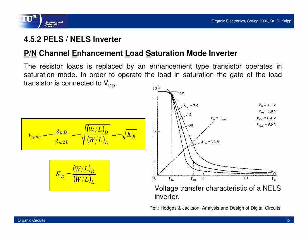
( )( ) R
L
D
Lm
mDgain K
LW
LW
gg
v −=−=−=2
( )( )L
DR LW
LWK =
Voltage transfer characteristic of a NELS inverter.
4.5.2 PELS / NELS Inverter
P/N Channel Enhancement Load Saturation Mode Inverter
The resistor loads is replaced by an enhancement type transistor operates in saturation mode. In order to operate the load in saturation the gate of the load transistor is connected to VDD.
Ref.: Hodges & Jackson, Analysis and Design of Digital Circuits
Organic Electronics, Spring 2006, Dr. D. Knipp
16Organic Circuits
4.5.2 PELS / NELS Inverter
P/N Channel Enhancement Load Saturation Mode Inverter
PELS or NELS inverters have the disadvantage that the output voltage in the high state is always smaller that operating voltage VDD. The output voltage is reduced by the effective threshold voltage. The effective threshold voltage is the threshold voltage which is influence by the bulk voltage which applied to the substrate.
Furthermore, the PELS / NELS inverters are limited by the differential drain source resistance of the load transistor. As the transistor operates in saturation the differential drain source resistance is rather large, which limits the switching speed of the inverter.
The differential drain source resistance can be reduced by operating the load transistor in the linear region. This can be achieved by using an additional voltage supply which provides a gate voltage for the load transistors. The reduced differential drain source resistance leads to an decreased switching speed of the inverter. However, the reduced differential drain source resistance leads to an increased power consumption of the inverter.
Organic Electronics, Spring 2006, Dr. D. Knipp
17Organic Circuits
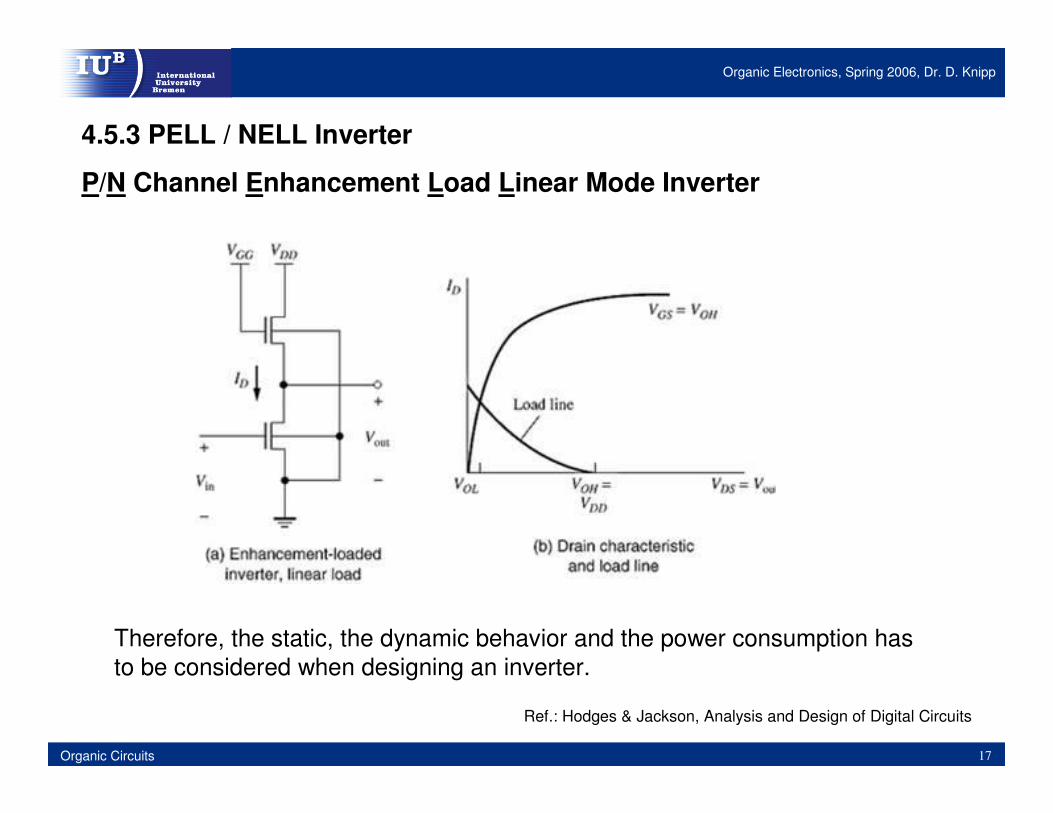
4.5.3 PELL / NELL Inverter
P/N Channel Enhancement Load Linear Mode Inverter
Therefore, the static, the dynamic behavior and the power consumption has to be considered when designing an inverter.
Ref.: Hodges & Jackson, Analysis and Design of Digital Circuits

Organic Electronics, Spring 2006, Dr. D. Knipp
18Organic Circuits
4.5.4 The CMOS Inverter
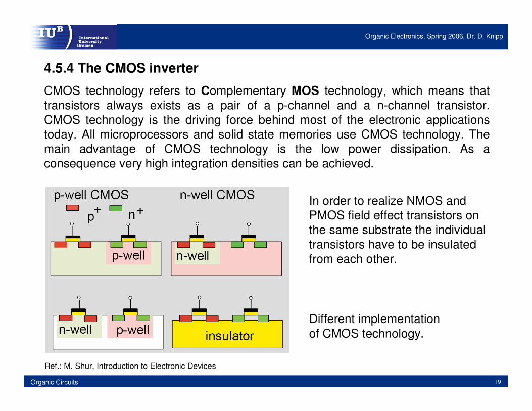
CMOS technology refers to Complementary MOS technology, which means that transistors always exists as a pair of a p-channel and a n-channel transistor. CMOS technology is the driving force behind most of the electronic applications today. All microprocessors and solid state memories use CMOS technology. The main advantage of CMOS technology is the low power dissipation. As a consequence very high integration densities can be achieved.
Organic Electronics, Spring 2006, Dr. D. Knipp
19Organic Circuits
4.5.4 The CMOS inverter
CMOS technology refers to Complementary MOS technology, which means that transistors always exists as a pair of a p-channel and a n-channel transistor. CMOS technology is the driving force behind most of the electronic applications today. All microprocessors and solid state memories use CMOS technology. The main advantage of CMOS technology is the low power dissipation. As a consequence very high integration densities can be achieved.
Ref.: M. Shur, Introduction to Electronic Devices
Different implementation of CMOS technology.
In order to realize NMOS and PMOS field effect transistors on the same substrate the individual transistors have to be insulated from each other.
Organic Electronics, Spring 2006, Dr. D. Knipp
20Organic Circuits
4.5.4 The CMOS inverter
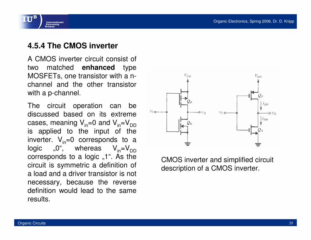
A CMOS inverter circuit consist of two matched enhanced type MOSFETs, one transistor with a n-channel and the other transistor with a p-channel.
The circuit operation can be discussed based on its extreme cases, meaning Vin=0 and Vin=VDDis applied to the input of the inverter. Vin=0 corresponds to a logic „0“, whereas Vin=VDDcorresponds to a logic „1“. As the circuit is symmetric a definition of a load and a driver transistor is not necessary, because the reverse definition would lead to the same results.
CMOS inverter and simplified circuit description of a CMOS inverter.

Organic Electronics, Spring 2006, Dr. D. Knipp
21Organic Circuits
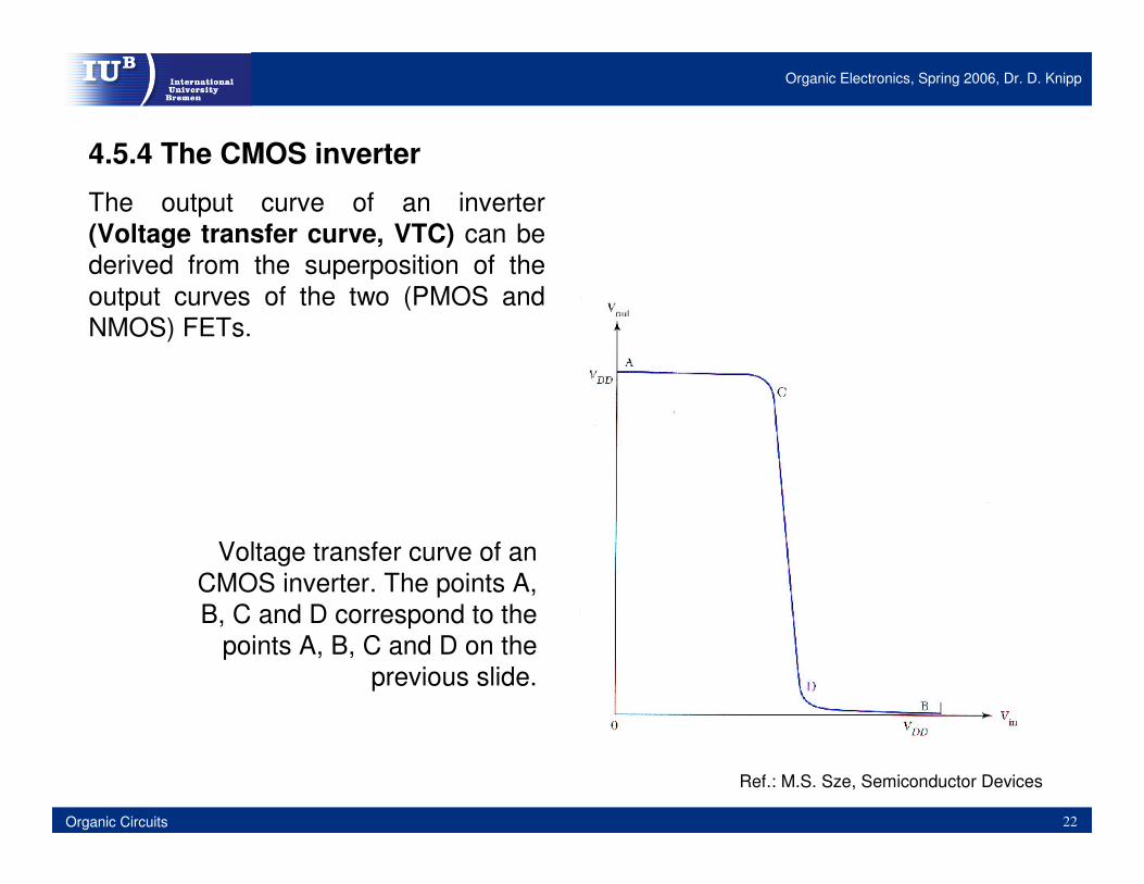
4.5.4 The CMOS inverter
The output curve of an inverter (Voltage transfer curve, VTC) can be derived from the superposition of the output curves of the two (PMOS and NMOS) FETs. The operating point of the inverter corresponds to the interceptions of the two output curves.
The interception of the output curves of the two MOSFETs of an inverter represent the output of the inverter.
Ref.: M.S. Sze, Semiconductor Devices
Organic Electronics, Spring 2006, Dr. D. Knipp
22Organic Circuits
Voltage transfer curve of an CMOS inverter. The points A, B, C and D correspond to the
points A, B, C and D on the previous slide.
4.5.4 The CMOS inverter
The output curve of an inverter (Voltage transfer curve, VTC) can be derived from the superposition of the output curves of the two (PMOS and NMOS) FETs.
Ref.: M.S. Sze, Semiconductor Devices

Organic Electronics, Spring 2006, Dr. D. Knipp
23Organic Circuits
4.5.4.1 Static power Dissipation
The static power dissipation of a CMOS inverter is negligible as always one of the two transistors is in the off state. The dissipation is independent of the input state of the inverter. The power dissipation of CMOS inverters is distinctly lower than the dissipation of alternative inverter circuits (e.g. NMOS or PMOS FETs in enhanced or depletion mode). However, as the number of gates steadily increases the dynamic power dissipation has become a serious issue.
4.5.4.2 Dynamic behavior of an CMOS inverter
The dynamic power dissipation can be determined by:
where f is the switching frequency. Cequi is the equivalent input capacitance of a CMOS inverter and VDD is the operating voltage.
2DDequiD VCfP ⋅⋅= Dynamic power dissipation
of an CMOS inverter
Organic Electronics, Spring 2006, Dr. D. Knipp
24Organic Circuits
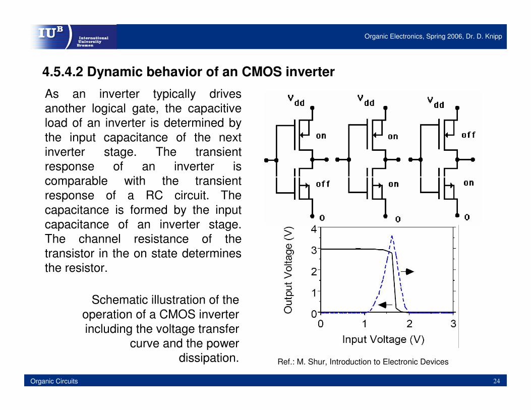
As an inverter typically drives another logical gate, the capacitive load of an inverter is determined by the input capacitance of the next inverter stage. The transient response of an inverter is comparable with the transient response of a RC circuit. The capacitance is formed by the input capacitance of an inverter stage. The channel resistance of the transistor in the on state determines the resistor.
Schematic illustration of theoperation of a CMOS inverterincluding the voltage transfer
curve and the powerdissipation. Ref.: M. Shur, Introduction to Electronic Devices
4.5.4.2 Dynamic behavior of an CMOS inverter
Organic Electronics, Spring 2006, Dr. D. Knipp
25Organic Circuits
4.5.4.3 Summary of CMOS inverter
Based on the above described device behavior we can summarize the ideal behavior of an CMOS inverter:
•The output levels should be either 0V or VDD. As a consequence the signal swing between the two levels should be maximized.
•The static power dissipation of an inverter is close to zero, if the leakage current of the transistors can be neglected. As a CMOS inverter is symmetric the power dissipation is independent of the logical output state.
•A low resistance path exists between the output terminal and ground (in the 0 state) or VDD (in the 1 state). The low resistance path ensures that the output voltage is independent of the transistor dimensions. As we use identical transistors for the driver and the load of the CMOS inverter a change of the dimensions of the FETs has no impact on the output voltage of the inverter.
•The input resistance of the inverter is infinite, because the input current is close to zero. Thus a large number of similar inverters can be driven with no loss on the signal level.

Organic Electronics, Spring 2006, Dr. D. Knipp
26Organic Circuits
4.6 From CMOS inverters to logical gates
Inverters are elementary components of digital logic circuits. All circuits can be reduced to inverter circuits. In the following the gained knowledge on CMOS inverters will be used to design simple logical CMOS circuits. We will concentrate here on basic structure, where the output signal is a direct combination of the input signals. Memory elements will not be taken into account.
Organic Electronics, Spring 2006, Dr. D. Knipp
27Organic Circuits
4.6 From CMOS inverters to logical gates
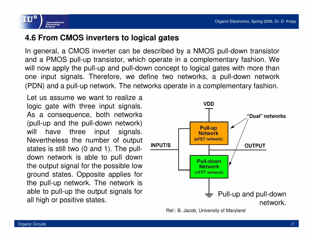
In general, a CMOS inverter can be described by a NMOS pull-down transistor and a PMOS pull-up transistor, which operate in a complementary fashion. We will now apply the pull-up and pull-down concept to logical gates with more than one input signals. Therefore, we define two networks, a pull-down network (PDN) and a pull-up network. The networks operate in a complementary fashion.
Pull-up and pull-down network.
Ref.: B. Jacob, University of Maryland
Let us assume we want to realize a logic gate with three input signals. As a consequence, both networks (pull-up and the pull-down network) will have three input signals. Nevertheless the number of output states is still two (0 and 1). The pull-down network is able to pull down the output signal for the possible low ground states. Opposite applies for the pull-up network. The network is able to pull-up the output signals for all high or positive states.

Organic Electronics, Spring 2006, Dr. D. Knipp
28Organic Circuits
4.6 From CMOS inverters to logical gates
Since the PDN comprises of NMOS transistors and the NMOS transistors conduct when the input signals is high, the PDN is active when the input signals are high. In a complementary manner, the PUN comprises PMOS transistors and PMOS transistors conduct when the input signal is low. Therefore the PUN is active for low input signals. Based on this scheme we can deduce the operation of logic gates like NOR, NAND, OR or AND.
Organic Electronics, Spring 2006, Dr. D. Knipp
29Organic Circuits
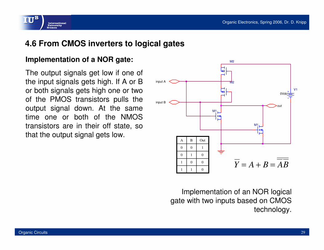
4.6 From CMOS inverters to logical gates
Implementation of an NOR logical gate with two inputs based on CMOS
technology.
Implementation of a NOR gate:
The output signals get low if one of the input signals gets high. If A or B or both signals gets high one or two of the PMOS transistors pulls the output signal down. At the same time one or both of the NMOS transistors are in their off state, so that the output signal gets low.
input A
M1
input B
V10Vdc
M2
out
M1
M2
011
001
010
100
OutBA
BABAY =+=
Organic Electronics, Spring 2006, Dr. D. Knipp
30Organic Circuits
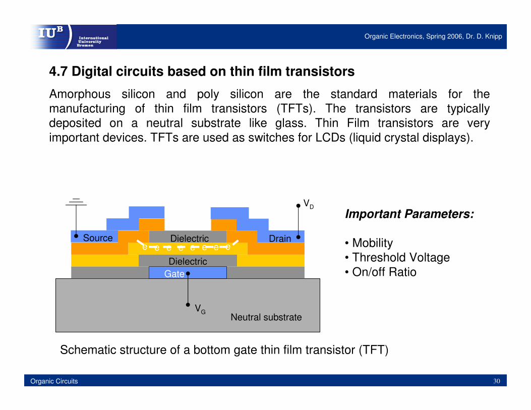
Important Parameters:
• Mobility• Threshold Voltage• On/off Ratio
Dielectric
Dielectrice e e e e e e e
Gate
VGNeutral substrate
Source Drain
VD
Schematic structure of a bottom gate thin film transistor (TFT)
4.7 Digital circuits based on thin film transistors
Amorphous silicon and poly silicon are the standard materials for the manufacturing of thin film transistors (TFTs). The transistors are typically deposited on a neutral substrate like glass. Thin Film transistors are very important devices. TFTs are used as switches for LCDs (liquid crystal displays).

Organic Electronics, Spring 2006, Dr. D. Knipp
31Organic Circuits
4.7 Digital circuits based on thin film transistors
The threshold voltage of a silicon transistor is defined to be the voltage applied to the gate for which an inversion layer is formed in the silicon substrate.
10-14
10-12
10-10
10-8
10-6
10-4
-40 -30 -20 -10 0 10 20 30
VD=-1V
VD=-30V
gate voltage [V]
drai
ncu
rrent
[A]
Organic thin film transistor
Mobility: ∼0.4cm/Vs
The definition of a threshold voltage for an thin film transistor is more complex as the transistor operates as accumulation type transistor. Furthermore, thin film transistors exhibit a pronounced sub threshold region. Such behavior complicates the design of circuits based on thin film transistors.
Transfer characteristic of a pentacene thin film transistor. The transistor exhibits a pronounced subthreshold region.
Organic Electronics, Spring 2006, Dr. D. Knipp
32Organic Circuits
4.7 Digital circuits based on thin film transistors4.7 Digital circuits based on thin film transistors
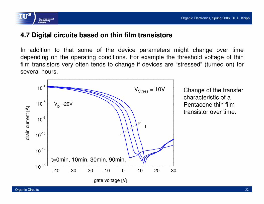
In addition to that some of the device parameters might change over time depending on the operating conditions. For example the threshold voltage of thin film transistors very often tends to change if devices are “stressed” (turned on) for several hours.
10-14
10-12
10-10
10-8
10-6
10-4
-40 -30 -20 -10 0 10 20 30
VD=-20V
t
gate voltage [V]
drai
n cu
rren
t [A
]
t=0min, 10min, 30min, 90min.
VStress = 10V Change of the transfer characteristic of a Pentacene thin film transistor over time.

Organic Electronics, Spring 2006, Dr. D. Knipp
33Organic Circuits
M1
M2
In
out
M4
M3
In
out
4.7 Digital circuits based on thin film transistors
In the case of (amorphous) silicon thin film transistors the electron carrier mobility is much than the hole mobilities. This prevents the realization of silicon thin film transistor based CMOS technology.
In the case of organic and polymeric materials the hole carrier mobility is usually much higher than the electron mobility, so that again the realization of organic CMOS technology is prevented.
In order to realize logic circuits PELS or NELS based circuits have to be realized.
Example of PELS or NELS based inverter.

Organic Electronics, Spring 2006, Dr. D. Knipp
34Organic Circuits
4.7 Digital circuits based on thin film transistors
Example of a pentacene based PELS inverter.
Ref.: G. Schmid, Infineon Technologies

Organic Electronics, Spring 2006, Dr. D. Knipp
35Organic Circuits
References
D.A. Hodges, Analysis and Design of Digital Integrated Circuits, McGraw-Hill Science/Engineering/Math (2003).(Price: US$150), Audience: undergraduate students
Michael Shur, Introduction to Electronic Devices, John Wiley & Sons; (January 1996).(Price: US$100), Audience: under graduate students
Simon M. Sze, Semiconductor Devices, Physics and Technology, John Wiley & Sons; 2nd Edition (2001). (Price: US$115), Audience: under graduate students
Adel S. Sedra, Kenneth C. Smith, Microelectronic Circuits, Oxford University Press (1998), (Price: 100-120 Euro).