Embed Size (px)
Citation preview
Dielectric spectroscopy at the nanoscale by atomic force microscopy: A simple modellinking materials properties and experimental responseLuis A. Miccio, Mohammed M. Kummali, Gustavo A. Schwartz, Ángel Alegría, and Juan Colmenero
Citation: Journal of Applied Physics 115, 184305 (2014); doi: 10.1063/1.4875836 View online: http://dx.doi.org/10.1063/1.4875836 View Table of Contents: http://scitation.aip.org/content/aip/journal/jap/115/18?ver=pdfcov Published by the AIP Publishing Articles you may be interested in Modeling of polar nanoregions dynamics on the dielectric response of relaxors J. Appl. Phys. 113, 224104 (2013); 10.1063/1.4809977 Numerical simulations of electrostatic interactions between an atomic force microscopy tip and a dielectricsample in presence of buried nano-particles J. Appl. Phys. 112, 114313 (2012); 10.1063/1.4768251 Intrinsic and extrinsic dielectric responses of CaCu3Ti4O12 thin films J. Appl. Phys. 110, 074102 (2011); 10.1063/1.3644962 Electrostatic response of hydrophobic surface measured by atomic force microscopy Appl. Phys. Lett. 82, 1126 (2003); 10.1063/1.1542945 The effect of force-field parameters on properties of liquids: Parametrization of a simple three-site model formethanol J. Chem. Phys. 112, 10450 (2000); 10.1063/1.481680
[This article is copyrighted as indicated in the article. Reuse of AIP content is subject to the terms at: http://scitation.aip.org/termsconditions. Downloaded to ] IP:
161.111.180.191 On: Mon, 29 Sep 2014 09:04:52
Dielectric spectroscopy at the nanoscale by atomic force microscopy:A simple model linking materials properties and experimentalresponse
Luis A. Miccio,1,2,3,a) Mohammed M. Kummali,1,3 Gustavo A. Schwartz,1,2 �Angel Alegr�ıa,1,3
and Juan Colmenero1,2,3
1Centro de F�ısica de Materiales (CSIC-UPV/EHU), P. M. de Lardizabal 5, 20018 San Sebasti�an, Spain2Donostia International Physics Center, P. M. de Lardizabal 4, 20018 San Sebasti�an, Spain3Departamento de F�ısica de Materiales (UPV/EHU), 20080 San Sebasti�an, Spain
(Received 18 February 2014; accepted 29 April 2014; published online 13 May 2014)
The use of an atomic force microscope for studying molecular dynamics through dielectric
spectroscopy with spatial resolution in the nanometer scale is a recently developed approach.
However, difficulties in the quantitative connection of the obtained data and the material dielectric
properties, namely, frequency dependent dielectric permittivity, have limited its application. In this
work, we develop a simple electrical model based on physically meaningful parameters to connect
the atomic force microscopy (AFM) based dielectric spectroscopy experimental results with the
material dielectric properties. We have tested the accuracy of the model and analyzed the relevance
of the forces arising from the electrical interaction with the AFM probe cantilever. In this way, by
using this model, it is now possible to obtain quantitative information of the local dielectric material
properties in a broad frequency range. Furthermore, it is also possible to determine the experimental
setup providing the best sensitivity in the detected signal. VC 2014 AIP Publishing LLC.
[http://dx.doi.org/10.1063/1.4875836]
I. INTRODUCTION
During the last decades, broadband dielectric spectros-
copy (BDS) has shown to be a very useful technique in the
study of the molecular dynamics of insulating materials. The
huge frequency range achieved (10�5–1012 Hz) and the pos-
sibility of measuring under different temperature, pressure,
and environmental conditions, allow the observation of a
large variety of processes with very different time scales.
Within this extraordinary experimental window, molecular
and collective dipolar fluctuations, charge transport and
polarization effects take place, in turn determining the
dielectric response of the material under study.1
In the last years, the growing interest in nanostructured
materials highlighted the need of measurements providing
local material properties. However, BDS cannot provide
direct information of these local features, due to the lack of
spatial resolution.
On the other hand, atomic force microscopy (AFM) pro-
vides outstanding spatial resolution of materials surface.2,3
In particular, electric force microscopy (EFM)4–10 can be
used for detecting local electrical interactions within these
materials. Recently, AFM has been used as the basis to de-
velop local dielectric spectroscopy (LDS).11 Within this
approach, the electrical interaction resulting by applying an
AC voltage to a conductive AFM probe is used to reveal in-
formation about the dielectric relaxation processes within the
material at local scale. Therefore, this technique combines
the capability of sensing the molecular dynamics with the
outstanding spatial resolution of AFM. These measurements
are based on a phase locked loop (PLL) setup11–14 and detect
the force gradient. In addition, a method based on the detec-
tion of the force was also recently developed, the so called
nanoDielectric Spectroscopy (nDS).15,16
As the detection in AFM based dielectric experiment
relies on the photodiode, the measured parameters are always
associated to the cantilever oscillation mechanics. In particu-
lar, in the force detection method, the measured parameters
are directly the root mean square (RMS) oscillation ampli-
tude, |VPh|, and the phase, h, of the photodiode signal.
However, the connection between the complex dielectric
permittivity of the material under study (namely e*(f)¼ e0(f)� i e00(f)) and the output signals of a nDS experiment is not
so straightforward. Thus, in order to explicitly establish this
connection, a physical model describing nDS experiments is
necessary. Although mathematical descriptions of the electri-
cal interaction between an AFM probe (upper electrode) and
a metallic lower electrode have been established17,18—
including the presence of a dielectric layer between the elec-
trodes19,20—to the best of our knowledge no such studies
related to the electrical phase and amplitude of force
detection-based dielectric spectroscopy have been done.
In order to successfully describe the dielectric losses in
local dielectric measurements, it is necessary to consider the
effect of the dielectric relaxations on the mechanical oscilla-
tion of the cantilever. Thus, by expressing the force on the
probe as a function of the dielectric properties of a given ma-
terial, a mathematical description of the cantilever RMS os-
cillation amplitude and phase for any electrical excitation
frequency can be carried out.
In this work, we propose a simple model to relate the
output of AFM based dielectric spectroscopy experiments
with the electrical properties of the sample, based on the
a)Author to whom correspondence should be addressed. Electronic mail:
0021-8979/2014/115(18)/184305/10/$30.00 VC 2014 AIP Publishing LLC115, 184305-1
JOURNAL OF APPLIED PHYSICS 115, 184305 (2014)
[This article is copyrighted as indicated in the article. Reuse of AIP content is subject to the terms at: http://scitation.aip.org/termsconditions. Downloaded to ] IP:
161.111.180.191 On: Mon, 29 Sep 2014 09:04:52
cantilever mechanics and the electrical interaction of the dif-
ferent parts of the probe. In a first step, we develop an equiva-
lent circuit model and the oscillation amplitude expressions
for the AFM probe. In a second step, we compare the data
obtained from the model with a gold surface (dissipation free
sample) and with a typical polymer film supported on it. As a
third step, we use the model to analyze the dependence of the
detected signal with the experimental parameters, and thereby
determine optimum conditions for the measurements. Finally,
in a fourth step, these predictions are evaluated by using spe-
cial AFM probes. Therefore, here we present a physically
meaningful model in order to quantitatively connect the sig-
nal detected in AFM based dielectric spectroscopy measure-
ments with the dielectric material properties.
II. THEORETICAL BACKGROUND
The EFM is based on the electrical force (Fe) resulting
from the interaction of a conductive AFM probe with charged
and/or polarizable entities in the material.5,6,18–23 Fe can be
evaluated by modeling the tip-sample system as a capacitor
(capacitance C): when a voltage (V) is applied, the resulting
electrostatic potential energy is W¼ 1=2CV2 and the corre-
sponding electrostatic force acting on the tip Fe¼ dW/dz(being z the coordinate along which the tip-sample distance is
measured). Consequently, when a sinusoidal voltage
[V(t)¼V0 sin(xet)] of frequency fe¼xe/2p is applied to the
AFM probe, the corresponding force is a sinusoidal function
given by
FeðtÞ ¼1
2
@C
@zVS þ VDC þ V0 sin xetð Þ½ �2; (1)
where VS is the surface potential and VDC is the applied DC
voltage (if any).15 Fe(t) has one component at a frequency
double than that used in the excitation due to the quadratic
relationship between Fe and V
F2xeðtÞ ¼ � 1
4
@C
@zV2
0 cos 2xetð Þ: (2)
The force amplitude and phase for this component depend
both on the experimental conditions and on the dielectric
properties of the material under investigation. Therefore, by
detecting the component of the probe motion at a frequency
double of the electrical excitation frequency, information
about the local dielectric relaxations of the materials under
investigation can be obtained. These measurements (nDS)
require the analysis of the signal from the AFM photodiode
with a Lock-In Amplifier (LIA) in order to obtain both the
amplitude |VPh| and electric phase h of the cantilever oscilla-
tions at 2xe (in this way, any component of the force at dif-
ferent frequencies is filtered). In the case of a loss-free
dielectric material, the signal amplitude brings information
on the static dielectric permittivity, which is frequency inde-
pendent. However, when dielectric relaxations take place in
a material, the dielectric permittivity becomes frequency de-
pendent and correspondingly a dielectric loss process will
appear (which in turn results in a complex capacitance) in
Eq. (2), which then becomes
F�2xeðtÞ ¼ � 1
4
@C�
@zV2
0 cos 2xetð Þ: (3)
Typically, a nDS experiment is performed at a single loca-
tion of the sample by employing the so called double-pass
method (DPM), where the measurements are performed in
two steps. In a first step, the sample topography is precisely
established in a standard “Tapping” mode experiment.
Subsequently, in lift mode, the mechanical cantilever excita-
tion is set to zero, in order to maintain a constant tip-sample
distance, and the probe motion generated by the tip-sample
interaction due to the application of an alternating voltage is
analyzed by the LIA. Thus, the LIA simultaneously provides
both the RMS oscillation amplitude (|VPh|) and the electrical
phase (h) of the cantilever response at 2xe. A reference
experiment on a dissipation free sample is performed for
each probe in order to precisely establish the reference elec-
tric phase (href) (the phase associated with the electronics
and the mechanical characteristics of the AFM probe).
Subsequently, the dielectric spectra are obtained by plotting
the phase shift (Dh), obtained by subtracting the reference
phase (href) from the original sample response (h), as a func-
tion of the electrical excitation frequency.
III. MODEL
In this section, we describe the modeling of the experi-
mental setup of nanoDielectric Spectroscopy. In a first step,
the effective capacitance between the AFM probe and the
lower electrode is defined by considering separately the con-
tributions from the three parts of the AFM probe: apex of the
tip, cone, and cantilever. Once these capacitances are known,
the force acting on the probe is numerically obtained from
Eq. (3). In the second step, expressions for the phase and the
oscillation amplitude are obtained by considering the cantile-
ver as a damped harmonic oscillator.
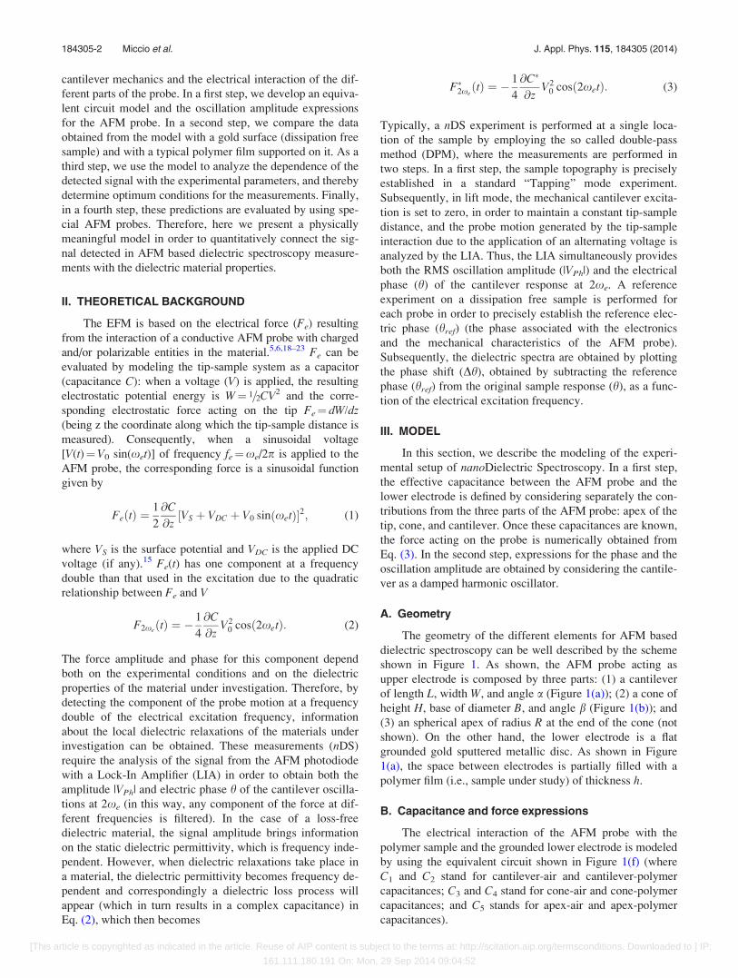
A. Geometry
The geometry of the different elements for AFM based
dielectric spectroscopy can be well described by the scheme
shown in Figure 1. As shown, the AFM probe acting as
upper electrode is composed by three parts: (1) a cantilever
of length L, width W, and angle a (Figure 1(a)); (2) a cone of
height H, base of diameter B, and angle b (Figure 1(b)); and
(3) an spherical apex of radius R at the end of the cone (not
shown). On the other hand, the lower electrode is a flat
grounded gold sputtered metallic disc. As shown in Figure
1(a), the space between electrodes is partially filled with a
polymer film (i.e., sample under study) of thickness h.
B. Capacitance and force expressions
The electrical interaction of the AFM probe with the
polymer sample and the grounded lower electrode is modeled
by using the equivalent circuit shown in Figure 1(f) (where
C1 and C2 stand for cantilever-air and cantilever-polymer
capacitances; C3 and C4 stand for cone-air and cone-polymer
capacitances; and C5 stands for apex-air and apex-polymer
capacitances).
184305-2 Miccio et al. J. Appl. Phys. 115, 184305 (2014)
[This article is copyrighted as indicated in the article. Reuse of AIP content is subject to the terms at: http://scitation.aip.org/termsconditions. Downloaded to ] IP:
161.111.180.191 On: Mon, 29 Sep 2014 09:04:52
The effective cantilever capacitance C�cantilever (C1 and C2, in Figure 1(f)) is obtained by considering a parallel plate capaci-
tor (of area Acantilever) for the polymer and a non-parallel plate capacitor for the air (Figure 1(e))
C�cantilever ¼ fBEðzþ HÞ � e0 �Wtan að Þ � ln 1þ L � sinðaÞ
zþ H
� � !�1
þ eo � e� � Acantilever
h
� ��1
24
35�1
: (4)
The border effects were introduced through a factor fBE
affecting the capacitance expression.24 Cone effective capac-
itance, C�cone, is also obtained by considering air and polymer
contributions separately. The expression for the cone-air ca-
pacitance (C3 in Figure 1(f)) arises from the integration of
concentric disks, as shown in Figure 1(c), while
cone-polymer capacitance is obtained by considering a disk
shaped parallel plate capacitor of thickness h and area
Acone(z), as schemed in Figure 1(d). In this case, the border
effects were introduced directly in the integration process as
a function of position (f BE zð Þ ¼ m0 � zþ n0). The resultant
expression is shown below:
C�cone ¼ 11 þ 12 þ 13ð Þ�1 þ e0 � e� � AconeðzÞh
� ��1" #�1
11 ¼e0 � p � m0
tanðbÞ2� B
2� R
� �
12 ¼e0 � p � n0
tanðbÞ3� B
2� R
� �
13 ¼e0 � p � n0
tanðbÞ3� z � ln
zþ R
tanðbÞ
zþ B
2 � tanðbÞ
0BBB@
1CCCA:
(5)
Finally, the effective apex capacitance is represented by
means of Eq. (6)17,20
C�apex ¼ 2p � e0 � R2 1þ R � ð1� sin h0Þ
zþ h
e�
24
35: (6)
The total force acting on the AFM probe is numerically
obtained from the previous capacitances according to
Eq. (2). Therefore, with this (probe-sample configuration)
AFM setup (Figure 1) it is possible to distinguish three force
contributions: (1) the force produced by the apex, (2) the
force produced by the cone, and (3) the force produced by
the cantilever. As a result, both real and imaginary parts of
the total force can be separately analyzed.
C. Oscillation amplitude and phase
Once the force acting on the probe is known, an approxi-
mated expression for the cantilever oscillation amplitude can
be obtained by assuming a harmonic oscillator behavior.25
This assumption is rather accurate for this kind of experi-
ments, where cantilever oscillation amplitude is substantially
low in comparison with the probe-sample distance (and the
driving force dependence with z can be safely neglected).
The phase of the cantilever oscillation signal with respect to
the excitation is obtained by considering the real and imagi-
nary parts of the damped harmonic oscillator amplitude. As
stated before, apex, cone, and cantilever contributions are
separately included in a single expression
h ¼ tan�1imðOsc�cantileverÞ þ imðOsc�coneÞ þ imðOsc�apexÞreðOsc�cantileverÞ þ reðOsc�coneÞ þ reðOsc�apexÞ
" #;
(7)
where Osc�cantilever, Osc�cone, and Osc�apex stand for the oscilla-
tion amplitude contribution from cantilever, cone, and apex,
respectively.
FIG. 1. Geometry of the cantilever-cone-apex/sample system for AFM-
based dielectric spectroscopy. (a) General scheme. (b) Zoom of the cone.
(c) Scheme of the integration of the cone capacitance. (d) Projected cone
area. (e) Scheme of the integration of the cantilever capacitance. (f)
Equivalent circuit model in nDS.
184305-3 Miccio et al. J. Appl. Phys. 115, 184305 (2014)
[This article is copyrighted as indicated in the article. Reuse of AIP content is subject to the terms at: http://scitation.aip.org/termsconditions. Downloaded to ] IP:
161.111.180.191 On: Mon, 29 Sep 2014 09:04:52
IV. RESULTS AND DISCUSSION
A. Model validation
In order to validate the proposed model, we employed
poly(vinyl acetate) (PVAc), a polymer with a prominent
dielectric relaxation detectable close to room temperature—
the so called a-relaxation. In a first step, we dielectrically
characterized the bulk polymer by means of BDS. In a second
step, we measured a film of this polymer by using nDS. The
thickness was set to about 350 nm, where literature data evi-
denced no thickness dependency on the a-relaxation,16,26–29
i.e., we should observe the same a-relaxation dielectric
response by both techniques. We then fixed the polymer
dielectric relaxation characteristics and used the here pro-
posed model to fit the obtained nDS data, leaving as fitting
parameters the apex radius, cone angle and cone base diame-
ter, among others. Finally, we independently measured these
parameters by using AFM and/or scanning electron micros-
copy (SEM) to test the model accuracy. This process was
repeated for both nDS signals, h and |Vph|.
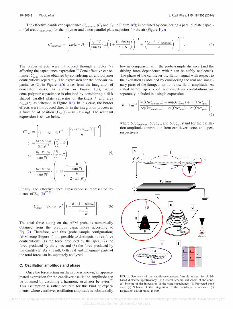
BDS characterization: Figure 2 shows the real and
imaginary parts of the complex dielectric permittivity (e0 and
e00, respectively) plotted as a function of frequency for bulk
PVAc, at temperatures ranging from 318 K to 373 K (experi-
mental details can be found in Appendix). A Havriliak-
Negami (HN) function30
e� ¼ e1 þ De � 1þ ðixsHNÞaHN� ��bHN (8)
was employed for the fitting procedures, as usual for this
kind of relaxations.1,31,32 Five HN fitting parameters were
obtained from the experimental curves at each temperature,
aHN and bHN (shape), De (intensity), sHN (relaxation time),
and e1 (high frequency permittivity).
nDS characterization: PVAc polymer films were meas-
ured by means of nDS at three different temperatures, where
PVAc a-relaxation is detectable within the current experi-
mental frequency window. As stated above, film thicknesses
were set to about 350 nm, and therefore the alpha relaxation
measured by nDS can be safely compared with its BDS
counterpart (i.e., the previously obtained HN parameters can
be used to describe the segmental relaxation in the polymer
films). Therefore, HN parameter values were used in the
model to describe the polymer relaxation within the studied
temperature range.
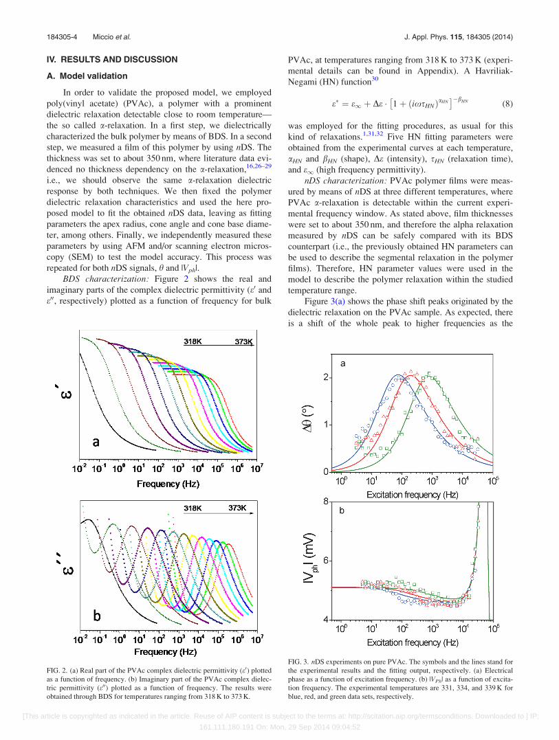
Figure 3(a) shows the phase shift peaks originated by the
dielectric relaxation on the PVAc sample. As expected, there
is a shift of the whole peak to higher frequencies as the
FIG. 2. (a) Real part of the PVAc complex dielectric permittivity (e0) plotted
as a function of frequency. (b) Imaginary part of the PVAc complex dielec-
tric permittivity (e00) plotted as a function of frequency. The results were
obtained through BDS for temperatures ranging from 318 K to 373 K.
FIG. 3. nDS experiments on pure PVAc. The symbols and the lines stand for
the experimental results and the fitting output, respectively. (a) Electrical
phase as a function of excitation frequency. (b) |VPh| as a function of excita-
tion frequency. The experimental temperatures are 331, 334, and 339 K for
blue, red, and green data sets, respectively.
184305-4 Miccio et al. J. Appl. Phys. 115, 184305 (2014)
[This article is copyrighted as indicated in the article. Reuse of AIP content is subject to the terms at: http://scitation.aip.org/termsconditions. Downloaded to ] IP:
161.111.180.191 On: Mon, 29 Sep 2014 09:04:52
temperature increases. Intensity and full width at half maxi-
mum (FWHM) are nearly the same for the three temperatures.
Lines in Figure 3(a) stand for the fitting results of the pro-
posed model. These fittings were performed simultaneously
for the three datasets, and apex radius, tip-sample distance,
cantilever angle, cone angle, cone base diameter were left as
free parameters. The so obtained values were R¼ 24.8 nm,
z0¼ 22.2 nm, B¼ 11.9 lm, a¼ 10�, and b¼ 15�.The rest of the parameters of the model were fixed dur-
ing the fitting procedure to the values obtained by direct
measuring (either by employing AFM or SEM for that pur-
pose). In addition, cone angle, cone base diameter, and tip
sample distance were also independently measured to obtain
a rough first validation of the fitting results.
The cantilever length and width were found to be about
250 lm and 30 lm (SEM). A cone height of 12 lm and an
angle of 15� were also determined by SEM. A typical tip-
sample distance during experiments of about 23 nm was also
found (for more details see Appendix), which is in close agree-
ment with the value obtained from the fitting (about 25 nm).
As stated before, in a nDS experiment, the RMS oscilla-
tion amplitude is obtained in addition to the electrical phase.
Therefore, it is possible to perform an additional validation
of the previously obtained parameters by also fitting jVphjresults. Figure 3(b) shows the experimental jVphj results
(symbols) and the corresponding fitting (lines). In this case,
the photodiode sensitivity (v) and the cantilever spring
constant (k) were the only free parameters. The obtained val-
ues are 16.4 mV/nm and 3 N/m, respectively. Apex radius,
tip-sample distance, cone height, and cantilever dimensions
were fixed from the previous fitting. As shown, the model
output is in close agreement with the experimental data.
In order to further confirm this second fitting procedure,
both sensitivity and spring constant were independently
measured by using the AFM (through force-distance curves
and thermal noise method,25 respectively). The obtained val-
ues 18.6 mV/nm and 2.7 N/m, respectively, are in close
agreement with the fitting results.
The obtained results show that the proposed model suc-
cessfully describes nDS experiments, therefore setting a con-
nection between the material dielectric properties and the
AFM parameters.
B. Model predictions
In this section, we use the above validated model to
study the influence of the experimental setup on nDS output.
In particular, we focus our attention on the influence of the
polymer film thickness in the detected phase shift.15
1. Contributions to the nDS phase
Apart from the spatial resolution, one of the most impor-
tant points of AFM based dielectric spectroscopy is the pos-
sibility of studying thin samples and the thickness effects on
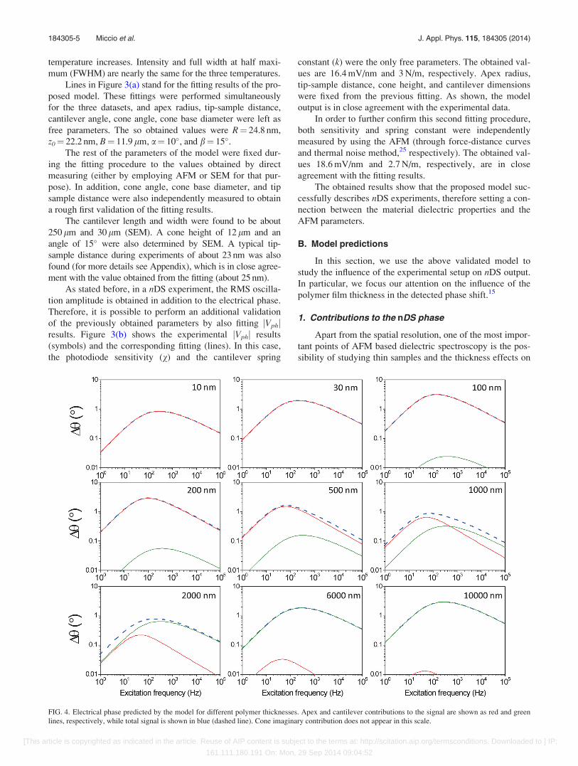
FIG. 4. Electrical phase predicted by the model for different polymer thicknesses. Apex and cantilever contributions to the signal are shown as red and green
lines, respectively, while total signal is shown in blue (dashed line). Cone imaginary contribution does not appear in this scale.
184305-5 Miccio et al. J. Appl. Phys. 115, 184305 (2014)
[This article is copyrighted as indicated in the article. Reuse of AIP content is subject to the terms at: http://scitation.aip.org/termsconditions. Downloaded to ] IP:
161.111.180.191 On: Mon, 29 Sep 2014 09:04:52
the polymer relaxation. However, in nDS measurements, the
direct influence of thickness on the measured signals, and
especially on the characteristics of the observed phase shifts,
is also a key factor. Figure 4 shows the model predictions at
331 K (based on the previously obtained parameters) for
PVAc films with thicknesses ranging from 10 nm to 10 lm.
Apex and cantilever contributions to the signal are shown as
red and green lines, respectively, while total signal is shown
with a blue (dashed) line. Although the cone signal is consid-
ered in the calculations, it is out of scale in Figure 4. This
point is further discussed below.
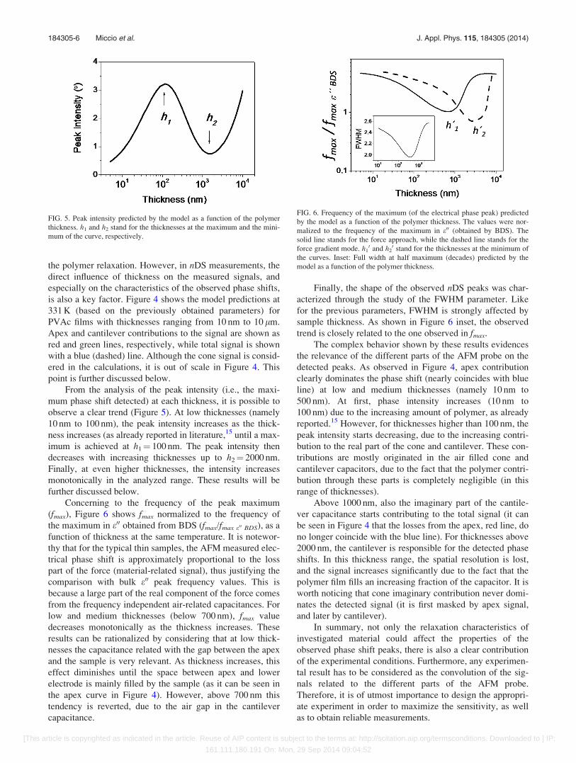
From the analysis of the peak intensity (i.e., the maxi-
mum phase shift detected) at each thickness, it is possible to
observe a clear trend (Figure 5). At low thicknesses (namely
10 nm to 100 nm), the peak intensity increases as the thick-
ness increases (as already reported in literature,15 until a max-
imum is achieved at h1¼ 100 nm. The peak intensity then
decreases with increasing thicknesses up to h2¼ 2000 nm.
Finally, at even higher thicknesses, the intensity increases
monotonically in the analyzed range. These results will be
further discussed below.
Concerning to the frequency of the peak maximum
(fmax), Figure 6 shows fmax normalized to the frequency of
the maximum in e00 obtained from BDS (fmax/fmax e00 BDS), as a
function of thickness at the same temperature. It is notewor-
thy that for the typical thin samples, the AFM measured elec-
trical phase shift is approximately proportional to the loss
part of the force (material-related signal), thus justifying the
comparison with bulk e00 peak frequency values. This is
because a large part of the real component of the force comes
from the frequency independent air-related capacitances. For
low and medium thicknesses (below 700 nm), fmax value
decreases monotonically as the thickness increases. These
results can be rationalized by considering that at low thick-
nesses the capacitance related with the gap between the apex
and the sample is very relevant. As thickness increases, this
effect diminishes until the space between apex and lower
electrode is mainly filled by the sample (as it can be seen in
the apex curve in Figure 4). However, above 700 nm this
tendency is reverted, due to the air gap in the cantilever
capacitance.
Finally, the shape of the observed nDS peaks was char-
acterized through the study of the FWHM parameter. Like
for the previous parameters, FWHM is strongly affected by
sample thickness. As shown in Figure 6 inset, the observed
trend is closely related to the one observed in fmax.
The complex behavior shown by these results evidences
the relevance of the different parts of the AFM probe on the
detected peaks. As observed in Figure 4, apex contribution
clearly dominates the phase shift (nearly coincides with blue
line) at low and medium thicknesses (namely 10 nm to
500 nm). At first, phase intensity increases (10 nm to
100 nm) due to the increasing amount of polymer, as already
reported.15 However, for thicknesses higher than 100 nm, the
peak intensity starts decreasing, due to the increasing contri-
bution to the real part of the cone and cantilever. These con-
tributions are mostly originated in the air filled cone and
cantilever capacitors, due to the fact that the polymer contri-
bution through these parts is completely negligible (in this
range of thicknesses).
Above 1000 nm, also the imaginary part of the cantile-
ver capacitance starts contributing to the total signal (it can
be seen in Figure 4 that the losses from the apex, red line, do
no longer coincide with the blue line). For thicknesses above
2000 nm, the cantilever is responsible for the detected phase
shifts. In this thickness range, the spatial resolution is lost,
and the signal increases significantly due to the fact that the
polymer film fills an increasing fraction of the capacitor. It is
worth noticing that cone imaginary contribution never domi-
nates the detected signal (it is first masked by apex signal,
and later by cantilever).
In summary, not only the relaxation characteristics of
investigated material could affect the properties of the
observed phase shift peaks, there is also a clear contribution
of the experimental conditions. Furthermore, any experimen-
tal result has to be considered as the convolution of the sig-
nals related to the different parts of the AFM probe.
Therefore, it is of utmost importance to design the appropri-
ate experiment in order to maximize the sensitivity, as well
as to obtain reliable measurements.
FIG. 5. Peak intensity predicted by the model as a function of the polymer
thickness. h1 and h2 stand for the thicknesses at the maximum and the mini-
mum of the curve, respectively.
FIG. 6. Frequency of the maximum (of the electrical phase peak) predicted
by the model as a function of the polymer thickness. The values were nor-
malized to the frequency of the maximum in e00 (obtained by BDS). The
solid line stands for the force approach, while the dashed line stands for the
force gradient mode. h10 and h2
0 stand for the thicknesses at the minimum of
the curves. Inset: Full width at half maximum (decades) predicted by the
model as a function of the polymer thickness.
184305-6 Miccio et al. J. Appl. Phys. 115, 184305 (2014)
[This article is copyrighted as indicated in the article. Reuse of AIP content is subject to the terms at: http://scitation.aip.org/termsconditions. Downloaded to ] IP:
161.111.180.191 On: Mon, 29 Sep 2014 09:04:52
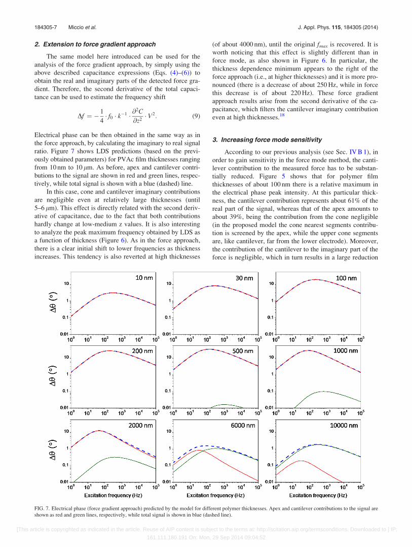
2. Extension to force gradient approach
The same model here introduced can be used for the
analysis of the force gradient approach, by simply using the
above described capacitance expressions (Eqs. (4)–(6)) to
obtain the real and imaginary parts of the detected force gra-
dient. Therefore, the second derivative of the total capaci-
tance can be used to estimate the frequency shift
Df ¼ � 1
4� f0 � k�1 � @
2C
@z2� V2: (9)
Electrical phase can be then obtained in the same way as in
the force approach, by calculating the imaginary to real signal
ratio. Figure 7 shows LDS predictions (based on the previ-
ously obtained parameters) for PVAc film thicknesses ranging
from 10 nm to 10 lm. As before, apex and cantilever contri-
butions to the signal are shown in red and green lines, respec-
tively, while total signal is shown with a blue (dashed) line.
In this case, cone and cantilever imaginary contributions
are negligible even at relatively large thicknesses (until
5–6 lm). This effect is directly related with the second deriv-
ative of capacitance, due to the fact that both contributions
hardly change at low-medium z values. It is also interesting
to analyze the peak maximum frequency obtained by LDS as
a function of thickness (Figure 6). As in the force approach,
there is a clear initial shift to lower frequencies as thickness
increases. This tendency is also reverted at high thicknesses
(of about 4000 nm), until the original fmax is recovered. It is
worth noticing that this effect is slightly different than in
force mode, as also shown in Figure 6. In particular, the
thickness dependence minimum appears to the right of the
force approach (i.e., at higher thicknesses) and it is more pro-
nounced (there is a decrease of about 250 Hz, while in force
this decrease is of about 220 Hz). These force gradient
approach results arise from the second derivative of the ca-
pacitance, which filters the cantilever imaginary contribution
even at high thicknesses.18
3. Increasing force mode sensitivity
According to our previous analysis (see Sec. IV B 1), in
order to gain sensitivity in the force mode method, the canti-
lever contribution to the measured force has to be substan-
tially reduced. Figure 5 shows that for polymer film
thicknesses of about 100 nm there is a relative maximum in
the electrical phase peak intensity. At this particular thick-
ness, the cantilever contribution represents about 61% of the
real part of the signal, whereas that of the apex amounts to
about 39%, being the contribution from the cone negligible
(in the proposed model the cone nearest segments contribu-
tion is screened by the apex, while the upper cone segments
are, like cantilever, far from the lower electrode). Moreover,
the contribution of the cantilever to the imaginary part of the
force is negligible, which in turn results in a large reduction
FIG. 7. Electrical phase (force gradient approach) predicted by the model for different polymer thicknesses. Apex and cantilever contributions to the signal are
shown as red and green lines, respectively, while total signal is shown in blue (dashed line).
184305-7 Miccio et al. J. Appl. Phys. 115, 184305 (2014)
[This article is copyrighted as indicated in the article. Reuse of AIP content is subject to the terms at: http://scitation.aip.org/termsconditions. Downloaded to ] IP:
161.111.180.191 On: Mon, 29 Sep 2014 09:04:52
of the measured phase value. Since in the parallel plate ca-
pacitor approximation, the derivative of the capacitance re-
sponsible for the force depends significantly on the
cantilever sample distance, the phase output in the force
mode method should be quite sensitive to an increase of the
cantilever/sample distance. In this regard, the use of espe-
cially designed AFM probes providing a larger cantilever/-
sample distance appears to be a very promising approach.
Commercial AFM probes providing larger cantilever/sample
distances already exist, like those manufactured by
Nauganeedles (NN-HAR-FM60, needle probe) consisting of
a conductive needle of about 10 lm at the end of the cone
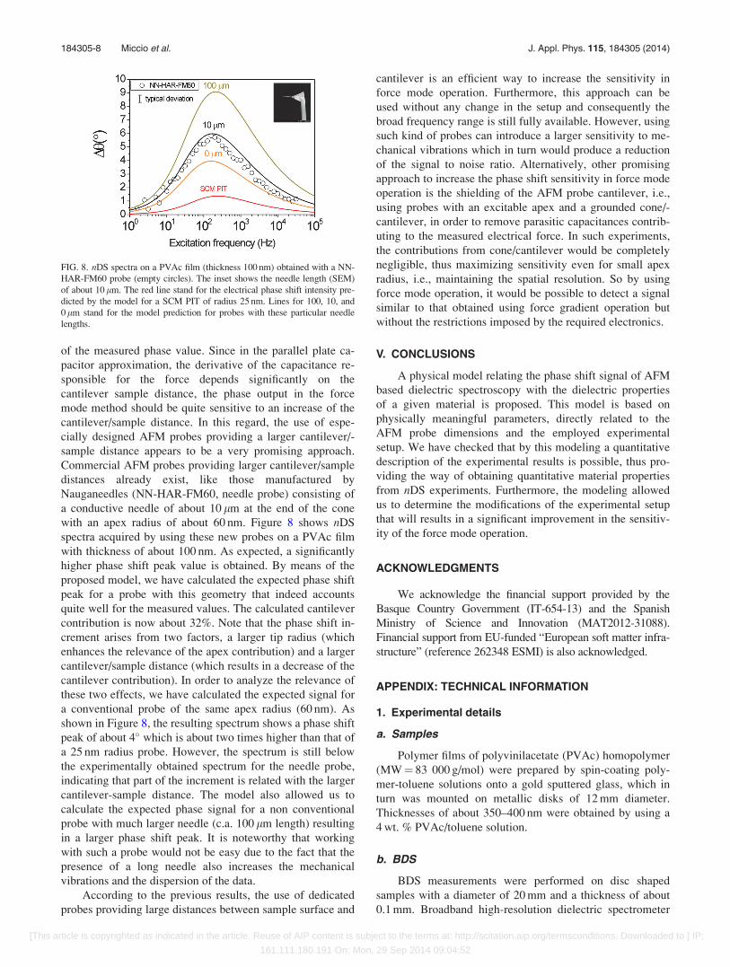
with an apex radius of about 60 nm. Figure 8 shows nDS
spectra acquired by using these new probes on a PVAc film
with thickness of about 100 nm. As expected, a significantly
higher phase shift peak value is obtained. By means of the
proposed model, we have calculated the expected phase shift
peak for a probe with this geometry that indeed accounts
quite well for the measured values. The calculated cantilever
contribution is now about 32%. Note that the phase shift in-
crement arises from two factors, a larger tip radius (which
enhances the relevance of the apex contribution) and a larger
cantilever/sample distance (which results in a decrease of the
cantilever contribution). In order to analyze the relevance of
these two effects, we have calculated the expected signal for
a conventional probe of the same apex radius (60 nm). As
shown in Figure 8, the resulting spectrum shows a phase shift
peak of about 4� which is about two times higher than that of
a 25 nm radius probe. However, the spectrum is still below
the experimentally obtained spectrum for the needle probe,
indicating that part of the increment is related with the larger
cantilever-sample distance. The model also allowed us to
calculate the expected phase signal for a non conventional
probe with much larger needle (c.a. 100 lm length) resulting
in a larger phase shift peak. It is noteworthy that working
with such a probe would not be easy due to the fact that the
presence of a long needle also increases the mechanical
vibrations and the dispersion of the data.
According to the previous results, the use of dedicated
probes providing large distances between sample surface and
cantilever is an efficient way to increase the sensitivity in
force mode operation. Furthermore, this approach can be
used without any change in the setup and consequently the
broad frequency range is still fully available. However, using
such kind of probes can introduce a larger sensitivity to me-
chanical vibrations which in turn would produce a reduction
of the signal to noise ratio. Alternatively, other promising
approach to increase the phase shift sensitivity in force mode
operation is the shielding of the AFM probe cantilever, i.e.,
using probes with an excitable apex and a grounded cone/-
cantilever, in order to remove parasitic capacitances contrib-
uting to the measured electrical force. In such experiments,
the contributions from cone/cantilever would be completely
negligible, thus maximizing sensitivity even for small apex
radius, i.e., maintaining the spatial resolution. So by using
force mode operation, it would be possible to detect a signal
similar to that obtained using force gradient operation but
without the restrictions imposed by the required electronics.
V. CONCLUSIONS
A physical model relating the phase shift signal of AFM
based dielectric spectroscopy with the dielectric properties
of a given material is proposed. This model is based on
physically meaningful parameters, directly related to the
AFM probe dimensions and the employed experimental
setup. We have checked that by this modeling a quantitative
description of the experimental results is possible, thus pro-
viding the way of obtaining quantitative material properties
from nDS experiments. Furthermore, the modeling allowed
us to determine the modifications of the experimental setup
that will results in a significant improvement in the sensitiv-
ity of the force mode operation.
ACKNOWLEDGMENTS
We acknowledge the financial support provided by the
Basque Country Government (IT-654-13) and the Spanish
Ministry of Science and Innovation (MAT2012-31088).
Financial support from EU-funded “European soft matter infra-
structure” (reference 262348 ESMI) is also acknowledged.
APPENDIX: TECHNICAL INFORMATION
1. Experimental details
a. Samples
Polymer films of polyvinilacetate (PVAc) homopolymer
(MW¼ 83 000 g/mol) were prepared by spin-coating poly-
mer-toluene solutions onto a gold sputtered glass, which in
turn was mounted on metallic disks of 12 mm diameter.
Thicknesses of about 350–400 nm were obtained by using a
4 wt. % PVAc/toluene solution.
b. BDS
BDS measurements were performed on disc shaped
samples with a diameter of 20 mm and a thickness of about
0.1 mm. Broadband high-resolution dielectric spectrometer
FIG. 8. nDS spectra on a PVAc film (thickness 100 nm) obtained with a NN-
HAR-FM60 probe (empty circles). The inset shows the needle length (SEM)
of about 10 lm. The red line stand for the electrical phase shift intensity pre-
dicted by the model for a SCM PIT of radius 25 nm. Lines for 100, 10, and
0 lm stand for the model prediction for probes with these particular needle
lengths.
184305-8 Miccio et al. J. Appl. Phys. 115, 184305 (2014)
[This article is copyrighted as indicated in the article. Reuse of AIP content is subject to the terms at: http://scitation.aip.org/termsconditions. Downloaded to ] IP:
161.111.180.191 On: Mon, 29 Sep 2014 09:04:52
(Novocontrol Alpha) was used to measure the complex
dielectric permittivity in the frequency range from 10�2 to
106 Hz. The sample temperature was controlled by nitrogen
gas flow which enables temperature stability of about
60.1 K.
c. AFM general setup
Topography and mechanical phase images were simul-
taneously obtained in moderate tapping mode, with an
Atomic Force Microscope MultiMode 8 (Bruker). The
measurements were performed using Antimony (Sb) doped
Si cantilevers, coated with Pt/Ir (SCM-PIT Bruker).
Nominal values for the natural frequency (f0), apex radius
(R), and cantilever spring constant (k) for the probes are
75 kHz, 20 nm, and 1.5–3 N/m, respectively. Proof of con-
cept experiments were conducted by using gold coated
NN-HAR-FM60 AFM probes (Nauganeedles). Nominal f0,
R, and k values for these probes are 60 kHz, 50 nm, and
3 N/m, respectively.
During AFM measurements, sample temperature was
controlled (from room temperature up to 150 �C) by using a
Thermal Applications Controller (TAC, Bruker). A silicone
cap was used as sealing to improve the thermal stabilization
of the system. The atmosphere inside the silicon cap was
controlled by using a dry nitrogen flow. An external LIA,
Stanford Research SR830 (frequency range up to 100 kHz)
was employed for EFM measurements.
d. nDS
Both electric phase and RMS amplitude were recorded
using a homemade LabVIEW routine. As previously men-
tioned, a reference experiment was performed over a gold
substrate without any polymer on it, (href). Dielectric spectra
were obtained by evaluating the phase shift (Dh), i.e.,
Dh¼ href - h, as a function of electrical excitation frequency.
2. Geometrical parameters
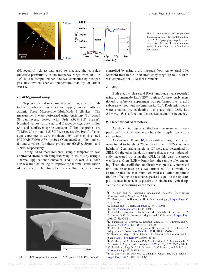
As shown in Figure 9, thickness measurements were
performed by AFM after scratching the sample film with a
sharp object.
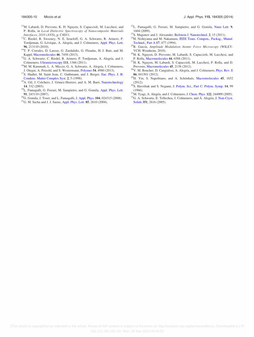
As shown in Figure 10, the cantilever length and width
were found to be about 250 lm and 30 lm (SEM). A cone
height of 12 lm and an angle of 15� were also determined by
SEM. On the other hand, tip sample distance was independ-
ently measured by using the AFM. In this case, the probe
was kept at 0 nm (LSH¼ 0 nm) from the sample after engag-
ing. Then, the oscillation amplitude was gradually increased
until the resonance peak was truncated. As a result, by
assuming that the maximum achieved oscillation amplitude
(before affecting the resonance peak) is equal to the tip sam-
ple distance in rest, it is possible to obtain the typical tip-
sample distance during experiments.
1F. Kremer and A. Schonhals, Broadband Dielectric Spectroscopy(Springer-Verlag, New York, 2003).
2Y. Martin, C. C. Williams, and H. K. Wickramasinghe, J. Appl. Phys. 61,
4723 (1987).3J. Tamayo and R. Garc�ıa, Langmuir 12, 4430 (1996).4G. Paul, Nanotechnology 12, 485 (2001).5C. Riedel, R. Arinero, P. Tordjeman, M. Ramonda, G. L�eveque, G. A.
Schwartz, D. G. De Oteyza, A. Alegria, and J. Colmenero, J. Appl. Phys.
106, 024315 (2009).6L. Fumagalli, G. Gramse, D. Esteban-Ferrer, M. A. Edwards, and G.
Gomila, Appl. Phys. Lett. 96, 183107 (2010).7C. Riedel, R. Arinero, P. Tordjeman, G. L�eveque, G. A. Schwartz, A.
Alegr�ıa, and J. Colmenero, Phys. Rev. E 81, 010801 (2010).8C. Riedel, A. Alegria, G. A. Schwartz, R. Arinero, J. Colmenero, and J. J.
Saenz, Appl. Phys. Lett. 99, 023101 (2011).9L. A. Miccio, M. M. Kummali, P. E. Montemartini, P. A. Oyanguren, G. A.
Schwartz, �A. Alegr�ıa, and J. Colmenero, J. Chem. Phys 135, 064704 (2011).10C. Riedel, A. Alegr�ıa, G. A. Schwartz, J. Colmenero, and J. J. S�aenz,
Nanotechnology 22, 285705 (2011).11P. S. Crider, M. R. Majewski, J. Zhang, H. Oukris, and N. E. Israeloff,
Appl. Phys. Lett. 91, 013102 (2007).
FIG. 9. Determination of the polymer
thickness by using the scratch method.
Left: AFM topography image (the lines
stand for the profile determination
paths). Right: Height as a function of
the position.
FIG. 10. SEM images of the conductive AFM probes (SCM PIT, Bruker).
184305-9 Miccio et al. J. Appl. Phys. 115, 184305 (2014)
[This article is copyrighted as indicated in the article. Reuse of AIP content is subject to the terms at: http://scitation.aip.org/termsconditions. Downloaded to ] IP:
161.111.180.191 On: Mon, 29 Sep 2014 09:04:52
12M. Labardi, D. Prevosto, K. H. Nguyen, S. Capaccioli, M. Lucchesi, and
P. Rolla, in Local Dielectric Spectroscopy of Nanocomposite MaterialsInterfaces, 2010 (AVS), p. C4D11.
13C. Riedel, R. Sweeney, N. E. Israeloff, G. A. Schwartz, R. Arinero, P.
Tordjeman, G. L�eveque, A. Alegr�ıa, and J. Colmenero, Appl. Phys. Lett.
96, 213110 (2010).14T. P. Corrales, D. Laroze, G. Zardalidis, G. Floudas, H.-J. Butt, and M.
Kappl, Macromolecules 46, 7458 (2013).15G. A. Schwartz, C. Riedel, R. Arinero, P. Tordjeman, A. Alegr�ıa, and J.
Colmenero, Ultramicroscopy 111, 1366 (2011).16M. M. Kummali, L. A. Miccio, G. A. Schwartz, A. Alegr�ıa, J. Colmenero,
J. Otegui, A. Petzold, and S. Westermann, Polymer 54, 4980 (2013).17S. Hudlet, M. Saint Jean, C. Guthmann, and J. Berger, Eur. Phys. J. B:
Condens. Matter Complex Syst. 2, 5 (1998).18A. Gil, J. Colchero, J. G�omez-Herrero, and A. M. Bar�o, Nanotechnology
14, 332 (2003).19L. Fumagalli, G. Ferrari, M. Sampietro, and G. Gomila, Appl. Phys. Lett.
91, 243110 (2007).20G. Gomila, J. Toset, and L. Fumagalli, J. Appl. Phys. 104, 024315 (2008).21G. M. Sacha and J. J. Saenz, Appl. Phys. Lett. 85, 2610 (2004).
22L. Fumagalli, G. Ferrari, M. Sampietro, and G. Gomila, Nano Lett. 9,
1604 (2009).23S. Magonov and J. Alexander, Beilstein J. Nanotechnol. 2, 15 (2011).24H. Nishiyama and M. Nakamura, IEEE Trans. Compon., Packag., Manuf.
Technol., Part A 17, 477 (1994).25R. Garc�ıa, Amplitude Modulation Atomic Force Microscopy (WILEY-
VCH, Weinheim, 2010).26H. K. Nguyen, D. Prevosto, M. Labardi, S. Capaccioli, M. Lucchesi, and
P. Rolla, Macromolecules 44, 6588 (2011).27H. K. Nguyen, M. Labardi, S. Capaccioli, M. Lucchesi, P. Rolla, and D.
Prevosto, Macromolecules 45, 2138 (2012).28V. M. Boucher, D. Cangialosi, A. Alegr�ıa, and J. Colmenero, Phys. Rev. E
86, 041501 (2012).29H. Yin, S. Napolitano, and A. Sch€onhals, Macromolecules 45, 1652
(2012).30S. Havriliak and S. Negami, J. Polym. Sci., Part C: Polym. Symp. 14, 99
(1966).31M. Tyagi, A. Alegr�ıa, and J. Colmenero, J. Chem. Phys. 122, 244909 (2005).32G. A. Schwartz, E. Tellechea, J. Colmenero, and �A. Alegr�ıa, J. Non-Cryst.
Solids 351, 2616 (2005).
184305-10 Miccio et al. J. Appl. Phys. 115, 184305 (2014)
[This article is copyrighted as indicated in the article. Reuse of AIP content is subject to the terms at: http://scitation.aip.org/termsconditions. Downloaded to ] IP:
161.111.180.191 On: Mon, 29 Sep 2014 09:04:52